
Rich interfacial chemistry and properties of carbon …...exhibit much different electronic...
26
Instructions for use Title Rich interfacial chemistry and properties of carbon-doped hexagonal boron nitride nanosheets revealed by electronic structure calculations Author(s) Xie, Wei; Tamura, Takahiro; Yanase, Takashi; Nagahama, Taro; Shimada, Toshihiro Citation Japanese Journal of Applied Physics (JJAP), 57(4), 04FL11 https://doi.org/10.7567/JJAP.57.04FL11 Issue Date 2018-04 Doc URL http://hdl.handle.net/2115/73356 Rights ©2018 The Japan Society of Applied Physics Type article (author version) File Information Xie2_JJAP_rev2.pdf Hokkaido University Collection of Scholarly and Academic Papers : HUSCAP
Transcript of Rich interfacial chemistry and properties of carbon …...exhibit much different electronic...

Instructions for use
Title Rich interfacial chemistry and properties of carbon-doped hexagonal boron nitride nanosheets revealed by electronicstructure calculations
Author(s) Xie, Wei; Tamura, Takahiro; Yanase, Takashi; Nagahama, Taro; Shimada, Toshihiro
Citation Japanese Journal of Applied Physics (JJAP), 57(4), 04FL11https://doi.org/10.7567/JJAP.57.04FL11
Issue Date 2018-04
Doc URL http://hdl.handle.net/2115/73356
Rights ©2018 The Japan Society of Applied Physics
Type article (author version)
File Information Xie2_JJAP_rev2.pdf
Hokkaido University Collection of Scholarly and Academic Papers : HUSCAP

Template for JJAP Regular Papers (Feb. 2017)
1
Rich interfacial chemistry and properties of carbon-doped hexagonal boron nitride nanosheets revealed by electronic structure calculations
Wei Xie1†, Takahiro Tamura1, Takashi Yanase1, Taro Nagahama1, Toshihiro
Shimada1*
1. Division of Applied Chemistry, Faculty of Engineering, Hokkaido University
Kita 13 Nishi 8, Kita-ku, Sapporo 060-8628, Japan
*E-mail: [email protected]
The effect of C doping to hexagonal boron nitride (h-BN) was examined by first principle
calculations with the association of π-electron systems of organic molecules embedded in a
two dimensional insulator. In mono-layered carbon doped structure, odd number doping
of carbon atoms lead to a metallic properties with different work functions. A variety of
electronic interactions was found in the interaction between two layers with odd number
carbon substitution. Direct sp3 covalent chemical bond is formed when C is replacing
adjacent B and N in the different layers. Charge transfer complex between layers was
found when the C is replacing next atoms, which results in narrow band gaps (e.g. 0.37eV).
Direct bonding between C and B atoms was found when two C atoms in different layers
are in distance.
†Present Address: Frontier Energy Research Division, Inamori Frontier Research Center,
Kyushu University

Template for JJAP Regular Papers (Feb. 2017)
2
1. Introduction Graphite and hexagonal boron nitride (h-BN) have analogous crystal structures but
exhibit much different electronic properties. Graphite is a metal with two unfilled bands
and h-BN is a wide band gap (Eg = 4.5eV) semiconductor. We can expect that a wide
variety of semiconductors with tunable band gaps will be synthesized by making their alloys
(hexagonal CxByNz; h-CBN) with well-defined structures. A variation of h-CBN is
gathering much attention recently as graphitic-C3N4 photocatalysts1), to which boron doping
is also attempted2). Considerable efforts are being made to synthesize monolayer h-CBN
using chemical vapor deposition on metal surfaces from methane and borazine3,4) or
sophisticated organic molecules5). These progresses stimulate our curiosity about the bulk
properties of carbon-doped h-BN. It should be noted that C-doped h-BN structures have
resemblance with π-conjugated organic molecules and stacking of h-CBN has analogy with
organic semiconductor crystals.
Recent theoretical works have revealed some of the interesting electronic structures of
h-CBNs.6-20) Single carbon dopant in h-BN makes midgap trap states, dopants tend to
aggregate, and substantial band dispersion is expected with multiple carbon doping. These
are uplifting results for the development of new group of semiconductors that are
light-weight and composed of naturally abundant elements. However, the theoretical
analyses of this important class of materials have been limited only to the graphene-like
monolayers of h-CBN.
Experimentally, however, distinct physical properties predicted by calculation have not
been confirmed well, despite the long history of research on this class of material21-25). The
primary reason is that the physical properties, such as work function and band gaps, are very
sensitive to the structural variation. Although it has been evaluated by computational
studies for monolayer h-CBNs, interlayer interaction has not been studied well. The main
purpose of this work is to clarify the electronic structures of double layer h-CBN. We briefly
extend our previous work20) on uneven substitution (h-CxByNz with y≠z) and then examine
the interlayer interaction of two layers. A part of this paper was presented in SSDM 2017
briefly without quantitative values of structural and electronic parameters,26) but this paper
explains the simulation results quantitatively and in more detail.

Template for JJAP Regular Papers (Feb. 2017)
3
2. Calculation methods All the calculations in this work were carried out on the Quantum-Espresso27) 5.1,
which is based on density-functional theory (DFT), plane wave and pseudopotentials.
VASP28) 5.3 was also used in some cases and the results were identical within the accuracy.
DFT was carried out with the exchange-correlation energy treated by the
Perdew-Burke-Ernzerhof (PBE) functional based on the generalized gradient
approximation (GGA). 29) Ultrasoft pseudopotentials 30) were used to describe the ionic
cores, and the electron wave function was expanded in plane wave with the cut-off energy
of 100 Ry for the geometry optimization and electronic structure calculations. The
mono-layered hybrid structures of h-CBN were modeled by a 4 × 4 h-BN supercell with 32
atoms, and the double-layered hybrid structures of h-CBN were also modeled by doping
carbon atoms to a 3 × 3 × 2 h-BN supercell with 36 atoms in a space group of P63/mmc.
More than 10Å vacuum space as periodic boundary conditions along c-axis avoids
interactions between layers in two neighboring cells. The atom positions were optimized
until the forces on each ions converged in 0.0001 a.u. and the energy was converged in 1.0
× 10-6 eV. The band structure, density of states (DOS) and the electron localization
function (ELF) 31,32) have been calculated by using the special k points of 9 × 9 × 1
(mono-layers) and 9 × 9 × 3 (double-layers) in the Brillouin zone of the supercell. 33) The
comparison with previous results of established materials systems have been described in
Ref. 20, which shows reasonable agreement.
3. Results and discussion 3.1 Unbalanced substitution in a monolayer
Single atom substitution of B or N by carbon atom gives half-filled flat midgap states as
reported in Ref. 16. A balanced substitution of B and N by multiple carbon atoms makes
intrinsic semiconductors. Here we calculated structures with odd-number substitution with
multiple carbon atoms. Typical examples of odd number substitutions are shown in Fig. 1.
Figures 1(a) and 1(b) are single atom substitution of B and N, respectively. Figures 1(c) and
1(d) show three atoms substitution of 3 B atoms by 3 C atoms and 3 N atoms by 3 C atoms,
respectively. Figures 1(e) and 1(f) shows substitution of 1 B atoms and 2 N atoms by 3 C
atoms, and 2 B atoms and 1 N atoms by 3 C atoms, respectively. The electronic band

Template for JJAP Regular Papers (Feb. 2017)
4
structures of these hypothetical materials are shown in Fig. 2. Figures 2(a) - 2(f)
corresponds to Fig. 1(a) - 1(f), respectively. The band structures in Fig. 2 are all metallic,
as expected from the odd numbers of electrons in the unit cell. It should be noted that the
Fermi levels indicated by horizontal broken lines are strongly dependent on which of B and
N are replaced more. It means that the work function values of these materials are
switchable in a wide range of 2 ~ 3 eV, which is an intriguing feature of them. It should
also be noted that the band dispersion increases by increasing the number of C atoms.
The small but finite band dispersion in Figs. 2(a) and 2(b) is different from the previously
reported flat impurity bands of single dopant cases15). The discrepancy is due to the
interaction between C atoms beyond the periodic boundary in the present calculation, of
which supercell is smaller than previous calculations.
In order to see how the influence of carbon dopants laterally propagates, Two
dimensional ELF (2D-ELF) were calculated for the further analysis. ELF is frequently
used to visualize chemical bonds explicitly31,32). Figure 3 shows the ELF distributions of
the monolayers shown in Fig. 1 in addition to pure h-BN (designated as “BN” in Fig. 3).
In pure h-BN, the boron and nitrogen atoms have totally different distributions of electrons,
i.e., the red area (high density of electron pairs) gathered around the nitrogen atoms, while
the blue area (low density of electron pairs) gathered around the boron atoms, which
reflects the difference in the nuclear charge. In the structure (a), the electron density
around the embedded carbon atom is intermediate between that around the boron atoms
and nitrogen atoms. The opposite situation in the structure (b), in which a carbon atom
substituted a nitrogen atom, a high electron density similar with nitrogen atoms is observed
around the carbon atom. In the structures (c) and (d), the three carbon atoms are
separately embedded in the h-BN system. The 2D-ELF distrubution around carbon atoms
in (c) and (d) are very similar to those in (a) and (b), which means that the three carbon
atoms have rather isolated electronic states. It is consistent with the band structures that
show small dispersion of carbon-derived bands. The last two 2D-ELF, Figs. 3(e) and 3(f),
correspond to the hybrid structures shown in Figs. 1(e) and 1(f), respectively. In Fig. 3(e),
the electron pair distribution around the carbon structures show the totally different shape
from the rest BN network which means that the embedded carbon structures formed a new
π-conjugated electron system. Furthermore, the electron pair distribution around the B and

Template for JJAP Regular Papers (Feb. 2017)
5
N adjacent to the carbon atoms are also modified. It corresponds to the band dispersion
modified in LUMO-1 and HOMO band in Fig. 2(e). Similar feature can be observed in
Fig. 3(f).
In the analysis above, the hybrid h-CBN systems with unbalanced substitution show
the metallic nature with very different electron affinity or work function values. This result
implies that a spontaneous electron transfer might occur by stacking differently doped
h-CBN. In the next section we will examine it.
3.2 Interaction between layers in double layers We examined the electronic structures of C-doped h-BN double layers. In the ordinary
h-BN (P63/mmc), the atoms in each layer are overlapped along c-axis, and B and N atoms
are stacked alternatingly. Figure 4 shows double-layered h-CBN structures studied in this
work. They are shown after the structural optimization. Figure 4(a) shows the case of the
nearest interlayer C-C distance, denoted as “2C-i” structure, in which two carbon atoms in
total substitute a B atom in the upper layer and an N atom in the lower layer. The C atoms
are stacked with the same position in the plane. Figures 4(b) and (c) depict the structures of
“2C-ii” and “2C-iii”, respectively. The difference among “2C-n“ (n = i,ii,iii) is the
distances between the carbon atoms. In 2C-ii and -iii, the C atom of the lower layer is shifted
toward (1 -1 0) direction by one atom and two atoms, respectively.
The optimized structures of these cases of single atom substitution per layer are much
different as observed in Fig. 4. In the “2C-i” case (Fig. 4(a)), in which carbon layer in the
different layer is nearest, carbon atoms come together to the distance of h2=1.67 Å. The
bond lengths of nearest intra-layer distances of C-N and C-B in the top and the bottom layers
are 1.47 Å and 1.56 Å, respectively. In the intermediate “2C-ii” case (Fig. 4(b)), the doped
carbon in the top layer deviated from the layer by h1=0.69Å toward the lower layer, while
that in the bottom layer had not shifted significantly, resulting in interlayer distance at the
shortest point to be h2=2.71 Å. In “2C-iii” structure (Fig. 4(c)), the doping carbon in top
layer have a significant deviation with the value of h1=0.82Å deviated from the top layer
while the carbon atom in bottom layer show no changes. Instead, a boron atom in the bottom
layer has shifted toward the top layer by h3=0.67 Å. This boron atom is just beneath the
carbon atom in the top layer, while nitrogen atom is on directly beyond the carbon atom in

Template for JJAP Regular Papers (Feb. 2017)
6
the bottom layer. It seems that this difference cause the apparent asymmetry of the behavior
of the carbon atoms. The interlayer C-B distance of the shifted pair is 1.76 Å. Based on
the structural information on “2C-i” and “2C-iii”, we can conclude that they have direct
chemical bonds between layers. The distance between interlayer C-C in “2C-i” (1.67Å) is
shorter than that of interlayer C-B in “2C-iii” (1.76Å), suggesting that the C-C bond is more
stable than C-B bonds.
We also calculated the structure with three doped carbon atoms per layer. “6C-i”
(Fig.4(d)) has the carbon atoms of the top and the bottom layers are facing to each other, in a
similar fashion with “2C-i”. The shortest interlayer C-C distance in “6C-i” is 1.67 Å, which
is the same value as that of “2C-i”. The bond lengths of C-N and C-B in top and bottom
layer are 1.47Å and 1.53Å in “6C-i” structure, respectively, which are similar to those of
“2C-i”. In “6C-ii” (Fig.4(e)) structure, the deviations of carbon from the layers have been
more weakened than in “2C-ii”. The displacement of carbon atoms from both layers is less
than 0.1Å, which is slightly less than “2C-ii”. The structure with three carbon atoms per
layer corresponding to “2C-iii” was not calculated because of the limitation of the supercell.
The band gaps of all the structures are listed in Table 1, which came from the band
structure calculation (shown in Fig. 5). In the structures “2C-i” and “6C-i” shown in Figs. 5
(a) and 5(b), respectively, the band gaps are great compared to other structures (3.75eV and
3.25eV, respectively). This result means that by stacking the two kinds of metallic layers
(B-rich h-CBN layer and N-rich h-CBN layer), the free electrons will pair together. The
band structures of “2C-ii” and “6C-ii are shown in Figs. 5 (c) and (d), respectively. The
both of them show small band gaps with the value of 0.36eV and 0.61eV, respectively. The
band gaps are much smaller than that of “2C-i” and “6C-i”. Although the carbon content
was increased from 2 to 6, the band gap of “6C-ii” increased from “2C-ii”, which is different
from the general tendency of monolayers or “2C-i” and “6C-i”. Both of “2C-ii” and “6C-ii”
are not metallic because neither of them have the energy levels crossing Fermi level. Figure
5(e) shows the bands structure of “2C-iii”. The band gap is indirect; the HOMO-band top is
located at Γ-point while LUMO-band bottom is located at K-point. The value of the band
gap is 2.69 eV. This band gap is also smaller than that of “2C-i” (3.75eV), but larger than that
of “2C-ii” (0.32eV). Interestingly, in the band structure of “2C-iii”, the HOMO crosses the
Fermi level, which means that structure “2C-iii” is metallic and unpaired electrons exist in

Template for JJAP Regular Papers (Feb. 2017)
7
this structure. From the analysis so far, the resemblances of electronic structures of “2C-i”
and “6C-i”, and “2C-ii” and “6C-ii” are apparent. Therefore, we will focus on the “2C-n”
(n = i,ii,iii) structures in the following.
The wave function distributions of HOMO and LUMOs are shown in Fig. 6. Figures 6
(a) and (b) exhibit the HOMO and LUMO of “2C-i”, respectively. HOMO of “2C-i” is
located on N atoms. LUMO is mainly located on the B atoms while a small part is located on
C atoms. The HOMO and LUMO are mainly contributed from B and N atoms adjacent to the
C atoms. It means that the C atoms change the electronic structure of neighboring B and N
atoms, and make them more active than other B and N atoms which are far away. In the
monolayers HOMO and LUMO are located on the C atoms, while in “2C-i” the contribution
of C atoms is weak. This result can be explained by considering that the sp3 carbon atoms
formed by interlayer bonding in “2C-i” have more stable electronic structures. HOMO and
LUMO of “6C-i” (not shown) have similar features as “2C-i”.
The HOMO and LUMO of “2C-ii” are shown in Figures 6(c) and (d), respectively. In
“2C-ii”, the HOMO and LUMO are mainly allocated at the C atoms. Both of C atoms
contribute to both of HOMO and LUMO, which means that the C atoms are active and they
can be both electron donors and acceptors. This mixed contribution of C atoms to both of
HOMO and LUMO seems important as the mechanism of narrowing band gaps with low
carbon content. This point will be discussed later using the charge and ELF distributions.
Finally, Figs.6 (e) and (f) shows the HOMO and LUMO of “2C-iii”. In this figure, HOMO is
mainly distributed in the top layer, around the N atoms adjacent to the doped C atom. On the
other hand, LUMO is distributed in the bottom layer, around the C atom and the N atom
adjacent to the C atom and N atoms around the displaced B atom. In the top layer, the
doped C atom neither contributes to the HOMO nor LUMO. Considering the displacement
of the C atom of the top layer, this C atom might have sp3 configuration, which has deep
levels.
In order to directly show the modification of electronic structure and the distributions of
electrons, especially interlayer electron transfer, ELF was calculated and the results are
shown in the following figures. In “2C-i” shown in Fig. 7, a large ELF cloud can clearly be
observed between two doped carbons along the C-C direction. It is the typical electron
distributions in σ-bonds, which means that in this structure “2C-i” the carbon atoms exist as

Template for JJAP Regular Papers (Feb. 2017)
8
sp3 carbons. It is reasonably understood that the band gap of “2C-i” is great because sp3
carbon have large energy gaps and do not contribute to narrow the band gap.
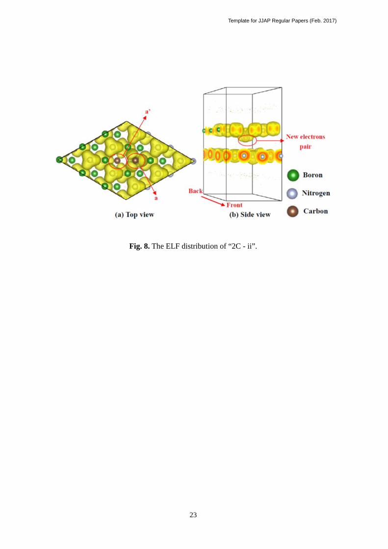
In the ELF figure of “2C-ii” shown in Fig 8, C atom a in the top layer (marked “a”) has
an electron cloud which is localized on the pz-orbital (z is perpendicular to the layer), in
addition to the three electron cloud along neighboring three N atoms. On the other hand,
the C atom in the bottom layer (marked “a’”), there are no electrons located at the pz-orbital.
It suggests that one electron is transferred from “a’” in the bottom layer to “a” in the top layer.
Indeed the electron counting indicates that 0.415 e- are donated from the bottom layer to the
top layer. In other words, “2C-ii” is a kind of charge-transfer (CT) complex. The narrow
band gap is naturally explained because it is one of the important features of the CT
complex 34).
Since the bandgap of “6C-ii” (0.61eV) is greater than that of “2C-ii” (0.36eV) but still
much smaller than that of BN (4.53eV), the tunability of CT complex was examined by
taking another example in “6C-ii”. In “6C-ii”, the shape of the electron distributions
between C-C (Fig. 9) means that beside the σ bonds, C-C is also contributed from π-electron
structures. The doped carbon atoms form two π-electron structures separately in different
layers. From this ELF figure, it is hard to tell where the new electron pair is located and the
direction of the electron transfer. In “6C-ii”, the electrons around C atoms are delocalized.
The new electron pair contributes to π-electron structures among the three carbons in the
same layer. By the close analysis, it was found that the electron transfer was from the bottom
layer to the top layer (N-rich layer to B-rich layer) and the amount was 0.32 e- in this
extended unit cell. This charge difference indicates that the spontaneous electron transfer
behavior still exists in “6C-ii” structure, but it is weakened. It is consistent with the bandgap
of “6C-ii” larger than “2C-ii”. Doping multiple (odd numbered) C atoms tend to form more
stable electronic structures in their own layers than isolated C atoms do.
In the ELF distribution of “2C-iii” shown in Fig.10, the existence of the electron cloud
between the C atom and underneath B atom means that these two atoms directly bond
together. Both of the C atom and the B atom exist with the stable sp3 state. It is the reason of
this C atom does not contribute to the HOMO or LUMO. The B atom, as a new electron
donor, forms covalent bond with the C atom. However, the other C atom in the bottom
layers (N-rich layer), an unpaired electron still located at the C atom, which makes the C

Template for JJAP Regular Papers (Feb. 2017)
9
atom more active than the C atom in the top layer. This is the reason of the metallic
features. The interlayer charge transfer exists in “2C-iii”, but the amount was 0.17 e-, which
is much smaller than those in type ii (i.e. “2C-ii” and “6C-ii”).
Finally, we examined the double-layered h-CBN with the even doping carbon number.
The results are not shown as figures, but the distance of the two layers after optimization
was 3.4 Å without any significant changes in vertical direction from pure double-layered
h-BN. The doped carbon atoms also did not show a significant position shift. Based on the
optimized structures, the two layers are independent. The band gap was 3.09eV. It is
noticed that all the band dispersion curves are made of almost parallel two curves; it is due to
the layered structure with very weak interaction.
Now we would like to comment on the comparison of the present results with the
experiments. h-CBN can be synthesized by CVD or plasma CVD but the electronic
structures are sensitive to the growth conditions35-37). We found that the electronic structures
are very sensitive to the geometry of the doping (C numbers, arrangements, etc.). It can
account for the difficulty to control the electronic structures of the materials. In the future,
some methods will be found to synthesize h-CBN as designed in the atomic level, and then it
will open a way to variety of physical properties of this group of materials. We hope the
present work will stimulate further experiments on the electronic structure of h-CBN system
as well as their applications. Once well-defined hexagonal B-C-N strucrtures can be
synthesized, the applications will be photo catalysts using tunable bandgaps, catalysts
using the partially localized electrons, and sensors with partial chemical bonding with
adsorbed molecules. Various experimental methods are now under development 38-41) for
the controlled synthesis.
4. Conclusions The effect of C doping to hexagonal boron nitride (h-BN) was examined by first
principle calculations with the association of π-electron systems of organic molecules
embedded in a two dimensional insulator. In mono-layered carbon doped structure, odd
number doping of carbon atoms lead to a metallic properties with different work functions.
Variety of electronic interactions was found in the interaction between two layers with odd

Template for JJAP Regular Papers (Feb. 2017)
10
number carbon substitution. Direct sp3 covalent chemical bond is formed when C is
replacing adjacent B and N in the different layers. Charge transfer complex between
layers was found when the C is replacing next atoms, which results in narrow band gaps
(e.g. 0.37eV). Direct bonding between C and B atoms was found when two C atoms in
different layers are in distance. The tunability of the band gap and the workfunction of
these materials will be very important for the application in electronics. It is desired to
develop methods to control the stoichiometry and local structure of the materials because
the electronic properties are sensitive to the local structures.
Acknowledgments
The present work has partly been supported by KAKENHI 17H0338007 and CREST-JST.
The authors thank the Supercomputer Center, the Institute for Solid State Physics, The
University of Tokyo for the use of the facilities.

Template for JJAP Regular Papers (Feb. 2017)
11
References 1) X.C. Wang, K. Maeda, A. Thomas, K. Watanabe, G.Xin., J.M. Carlsson, K.Domen, and
M. Antonietti, Nat. Mater. 5, 76 (2009).
2) S.C.Yang, Z.S.Li, and Z.G. Zou, Langmuir 26, 3894 (2010).
3) L. Ci, L. Song, C. Jin, D. Jariwala, D. Wu, Y. Lim A. Srivastava, Z.F. Wang, K. Storr, L.
Balicas, F. Liu, and P.M. Ajayan, Nat. Mater. 9, 430 (2010).
4) C. Zhang, S. Zhao, C. Jin, A.L.Koh, Y. Zhou, W. Xu, Q. Li, Q. Xiong, H. Peng, and Z.
Liu, Nat. Commun. 6:6519 (2015).
5) C. Sanchez-Sanchez, S. Bruller, H.Sachdev, K. Mullen, M. Krieg, H.F. Betinger, A.
Nicolai,V. Meunier, L. Talirz, R. Fasel, and P. Ruffieux, ACS Nano 9, 9228 (2015).
6) M.S.C. Mazzoni, R.W. Nunes, S.Azevedo, and H.Chacham, Phys. Rev. B 73, 073108
(2006).
7) K. Yuge, Phys. Rev. B79, 144109(2009).
8) Y. Ding, Y. Wang, and J. Ni, Appl. Phys. Lett. 95, 123105(2009).
9) P.P. Shinde, and V. Kumar, Phys. Rev. B 84, 125401(2011).
10) A.K. Manna, and S.K. Pati, J. Phys. Chem. C 115, 10842 (2011).
11) Q.Peng, and S. De, Physica E44, 1662 (2012).
12) M. Ni, Y. Wang, Q.Yang, Q.Zhu,Q.Tang, and Z. Li, Mod. Phys. Lett. B 28, 1450144
(2014).
13) J. Beheshtian, H. Soleymanabadi, A.A. Peyghan, and Z. Bagheri, Appl. Surf. Sci. 268,436
(2013).
14) M. Kan, J. Zhou, Q. Wang, Q.Sun, and P. Jena, Phys. Rev. B84, 205412 (2011).
15) H. Park, A. Wadehra, J.W. Wilkins, and A.H. Castro Neto, Appl. Phys. Lett. 100,
253115 (2012).
16) Y. Xie, H. Yu, H.X. Zhang, and H.G. Fu, Phys. Chem. Chem. Phys. 14,4391(2012).
17) A. Ramasubramaniam, and D. Naveh, Phys. Rev. B84, 075405 (2011).
18) M.G.Menezes, and R.B. Capaz, Phys. Rev. B86, 195413 (2012).
19) B. Muchharla, A. Pathak, Z. Liu, L. Song, T. Jayasekera, S. Kar, R. Vajtai,L. Balicas, P.M.
Ajayan, and S. Talapatra, Nano Lett. 13, 3476 (2013).
20) W.Xie, T. Yanase, T. Nagahama, and T.Shimada, C - J. Carbon Research 2,2 (2016).
21) M. Terrones, N. Grobert, and H. Terrones, Carbon 40, 1665 (2002).

Template for JJAP Regular Papers (Feb. 2017)
12
22) A. Vinu, T. Mori, and K. Ariga, Sci. Tech. Adv. Mater. 7, 753 (2006).
23) R.Z. Ma, D. Goldberg, Y. Bando, and T. Sasaki, Phil.Trans. Roy. Soc. London Ser. A 361,
2161 (2004).
24) A.M.Alexander, and J.S.J. Hargreaves, Chem. Soc. Rev. 39, 4388 (2010).
25) T.Tamura, T. Yanase, T. Nagahama, M. Wakeshima, Y. Hinatsu, and T.Shimada,
Chem.Lett. 43, 1569 (2014).
26) W. Xie, T. Tamura, T. Yanase, T. Nagahama, and T. Shimada, Ext. Abs. of SSDM2017,
B-3-04 (2017).
27) P. Giannozzi, S. Baroni, N. Bonini, M. Calandra, R. Car, C. Cavazzoni, D. Ceresoli, G.L
Chiarotti, M.Cococcioni, and I. Dabo, J. Phys. 21, 395502 (2009)
28) G. Kresse, and J. Furthmuller, Phys.Rev.B 54 11169(1996).
29) Q.B.Wang, C.Zhou, J. Wu, T.Lu, and K.H.Je, Comput. Mater. Sci. 102, 196 (2015).
30) M. Etienne, A. Quach, D. Grosso, L. Nicole, C. Sanchez, and A. Walcarius, Chem. Mater.
19, 844 (2007).
31) H.J. Monkhorst and J.D. Pack, Phys. Rev. B13, 5188 (1976).
32) A. D. Becke and K. E. Edgecombe, J. Chem. Phys. 92, 5397 (1990).
33) A. Savin, O. Jepsen, J. Flad, O.K. Andersen, H. Preuss and H.G. von Schnering, Angew.
Chem. Int. Ed. 31, 187 (1992).
34) H. Murakami, Bull.Chem.Soc. Jpn. 28, 577 (1955).
35) L. Filipozzi, A. Derre, J. Conard, L. Piraux, and A. Marchand, Carbon 33, 1747 (1995).
36) L. Filipozzi, L. Piraux, A. Marchand, A. Derre, A. Adouard, and M. Kinany-Alaoui, J.
Mater. Res. 12, 1711(1997).
37) A. Prakash, and K.B. Sundaram, ECS J. Solid State Sci. & Technol. 4, N25 (2015).
38) T. Tamura, T. Takami, T. Yanase, T. Nagahama, and T. Shimada, Jpn. J. Appl. Phys. 56,
06HF01 (2017).
39) T. Tamura, T. Takami, S. Kobayashi, T. Nagahama, T. Yanase, and T. Shimada, Diamond
and Related Materials 69,127 (2016).
40) W. Xie, A. Kawahito, T. Miura, T. Endo, Y. Wang, T. Yanase, T. Nagahama, Y. Otani, and
T. Shimada, Chem. Lett. 44 , 1205 (2015).
41) T. Tamura, T. Yanase, T. Nagahama, M. Wakeshima, Y. Hinatsu, and T. Shimada, Chem.
Lett. 43, 1569(2014).

Template for JJAP Regular Papers (Feb. 2017)
13
Figure Captions Fig. 1. (Color Online) Typical examples of odd number substitutions. (a) A carbon atom
replaces a boron atom. (b) A carbon atom replaces a nitrogen atom. (c) Three carbon atoms
replace three boron atoms. (d) Three carbon atoms replace three nitrogen atoms. (e)
Three carbon atoms replace a boron atom and two nitrogen atoms. (f) Three carbon
atoms replace two boron atoms and a nitrogen atom.
Fig. 2. (Color Online) The electronic band structures of the hypothetical materials.
Figures 2(a) - 2(f) correspond to Figs. 1(a) - 1(f), respectively.
Fig. 3. (Color Online) 2D-electron localization function (ELF) distribution of the
monolayer h-CBN structures. (a)-(f) correspond to those in Figs.1 and 2 as shown in the
insets.
Fig. 4. (Color Online) The optimized structures of the double-layered h-CBN structures.
(a) “2C-i”, (b) “2C-ii”, (c) “2C-iii”, (d) “6C-i”, and (e) “6C-ii”. See main text for the
naming rule.
Fig. 5. (Color Online) Band structures of the double-layered h-CBN structures. (a)-(e)
correspond to those of Fig.4.
Fig. 6. (Color Online) HOMO and LUMO of the double-layered structures. (a) HOMO
and (b)LUMO of “2C-i”. (c) HOMO and (d) LUMO of “2C-ii”. (e) HOMO and (f) LUMO
of “2C-iii”.
Fig. 7. (Color Online) The ELF of “2C-i”. The two doped carbon atoms shifted from their
layers and get close. The ELF cloud can be observed between these two doping carbon
along the C-C direction which means the C-C bonds formed and it is the σ-bonds.
Fig. 8. (Color Online) The ELF distribution of “2C-ii”.

Template for JJAP Regular Papers (Feb. 2017)
14
Fig. 9. (Color Online) The ELF distribution of “6C-ii”. In the bottom layer, the doping
three carbon gathered more electron than the top layer.
Fig. 10. (Color Online) The ELF distribution of “2C-iii”

Template for JJAP Regular Papers (Feb. 2017)
15
Table 1: Bandgaps and nearest interlayer distances of the unevenly substituted double layer h-BNs Structure “2C-i” “6C-i” “2C-ii” “6C-ii” “2C-iii” Bandgap (eV) 3.75 3.25 0.36 0.61 2.69 Nearest Interlayer (Å) 1.67 1.67 2.71 2.70 1.76 Distance

Template for JJAP Regular Papers (Feb. 2017)
16
Fig. 1. (Color Online) Typical examples of odd number substitutions. (a) A carbon atom
replaces a boron atom. (b) A carbon atom replaces a nitrogen atom. (c) Three carbon atoms
replace three boron atoms. (d) Three carbon atoms replace three nitrogen atoms. (e)
Three carbon atoms replace a boron atom and two nitrogen atoms. (f) Three carbon
atoms replace two boron atoms and a nitrogen atom.

Template for JJAP Regular Papers (Feb. 2017)
17
Fig. 2. (Color Online) The electronic band structures of the hypothetical
materials. Figures 2(a) - 2(f) correspond to Figs. 1(a) - 1(f), respectively.

Template for JJAP Regular Papers (Feb. 2017)
18
Fig. 3. (Color Online) 2D-electron localization function (ELF) distribution of the
monolayer h-CBN structures. (a)~(f) correspond to those in Figs.1 and 2 as shown in the
insets.

Template for JJAP Regular Papers (Feb. 2017)
19
Fig. 4. (Color Online) The optimized structures of the double-layered h-CBN structures.
(a) “2C-i”, (b) “2C-ii”, (c) “2C-iii”, (d) “6C-i”, and (e) 6C-ii. See main text for the naming
rule.

Template for JJAP Regular Papers (Feb. 2017)
20
Fig. 5. (Color Online) Band structures of the double-layered h-CBN structures. (a)-(e)
correspond to those of Fig.4.

Template for JJAP Regular Papers (Feb. 2017)
21
Fig. 6. (Color Online) HOMO and LUMO of the double-layered structures.
(a) HOMO and (b)LUMO of “2C-i”. (c) HOMO and (d) LUMO of “2C-ii”. (e) HOMO and
(f) LUMO of “2C-iii”.

Template for JJAP Regular Papers (Feb. 2017)
22
Fig. 7. (Color Online) The ELF distrubution of “2C-i”. The two doped carbon atoms
shifted from their layers and get close. The ELF cloud can be observed between these two
doping carbon along the C-C direction which means the C-C bonds formed and it is the
σ-bonds.
Template for JJAP Regular Papers (Feb. 2017)
23
Fig. 8. The ELF distribution of “2C - ii”.

Template for JJAP Regular Papers (Feb. 2017)
24
Fig. 9. The ELF distribution of “6C-ii”. In the bottom layer, the doping three carbon
gathered more electron than the top layer.

Template for JJAP Regular Papers (Feb. 2017)
25
Fig. 10. The ELF distribution of “2C - iii”.


![CB,HBI,HBN目錄 2019.02.27 (宏聯)¼CBI/HBI/HBN... · 4 - - Nominal flow rate [m³/h] 3 0 HQBE (HBI ) HQQE (HBN ) Number of stages x10 Mechanical Seals HBI (N) 8 , 12 8 - 1](https://static.fdocuments.in/doc/165x107/5f06dfae7e708231d41a29ed/cbhbihbnceoe-20190227-e-cbiihbiihbn-4-nominal-flow-rate.jpg)


