
RFID Refrigerator Organizer - WINLABcrose/428_html/projects11/RFIDFridge.pdf · 1. Abstract The...
39
RFID Refrigerator Organizer Wireless Senior Capstone Design Advisor: Christopher Rose By Eric Wasserman Nishit Raval Hiran Patel Date: May 2, 2011
Transcript of RFID Refrigerator Organizer - WINLABcrose/428_html/projects11/RFIDFridge.pdf · 1. Abstract The...

RFID Refrigerator Organizer
Wireless Senior Capstone Design
Advisor: Christopher Rose
By
Eric Wasserman
Nishit Raval
Hiran Patel
Date: May 2, 2011

Table of Contents 1. Abstract ...............................................................................................................................3
2. Theory ....................................................................................................................................4
2.1 RFID Tag ...........................................................................................................................4
2.1.1 Voltage Multiplier.........................................................................................................5
2.1.2 Voltage Regulator .......................................................................................................8
2.1.3 Demodulator ...............................................................................................................9
2.1.4 Clock Generator ........................................................................................................10
2.1.5 Power on Reset ........................................................................................................11
2.1.6 Bias Circuit ................................................................................................................11
2.1.7 Modulator ..................................................................................................................11
2.1.8 Impedance Matching Proof .......................................................................................13
2.1.9 Backscattered Subcarrier Modulation ........................................................................14
2.1.10 Signal Processing Unit ............................................................................................15
2.2 RFID Reader ...................................................................................................................16
2.2.1 Transmitter ................................................................................................................17
2.2.2 Receiver ....................................................................................................................17
2.2.3 Protocol .....................................................................................................................26
3. Procedure ............................................................................................................................28
3.1 Initial Procurement and Installation ..................................................................................28
3.2 Testing / Adjustments ......................................................................................................28
3.3 Code Modifications ..........................................................................................................29
3.4 GUI Application................................................................................................................30
4. Technical Specifications .......................................................................................................30
4.1 USRP ..............................................................................................................................30
4.2 RFID Tags .......................................................................................................................31
4.3 Antenna ...........................................................................................................................31
6. Conclusion ...........................................................................................................................33
7. Division of Labor ..................................................................................................................33
8. References...........................................................................................................................34
9. Pictures ................................................................................................................................35
Appendix ...................................................................................................................................39

1. Abstract The purpose of the RFID Refrigerator Organizer is to design a system that can keep
track of food products in a refrigerator. The food products will be tracked using a RFID
reader/tag system and will allow the user to access this information from a Java application.
Our procedure includes the following goals:
1. Build an RFID reader using open source software available through GNU Radio and the
Universal Software Radio Peripheral (USRP).
2. Implement the RFID reader to communicate with RFID tags attached to each food product.
3. Design an application that allows the user to see which food products are currently available,
when the reader last polled the tags, when the user first placed the item in the refrigerator, and
view a list of products which the user should purchase.

2. Theory
2.1 RFID Tag
A UHF (900 MHz) passive RFID tag consists of an antenna and an Integrated Circuit
(IC) chip. The antenna is approximately 16 cm or half the wavelength of the 900 MHz carrier
signal sent by the reader. Each RFID tag has a slightly different IC, but most follow a similar
architecture to the one shown in figure 1. There are two main components of the IC chip, the
RF front end and the signal processing unit.
The RF front end performs the following three operations:
● Convert the incoming RF signal to DC current voltage which will be used to power the
clock generator, the digital end, the bias circuit, and the power on reset.
● Demodulate the incoming RF signal and pass the data to the digital end.
● Take the data from the digital end, modulate it with the continuous wave from the reader,
and effectively backscatter the data back to the reader.
The second component of the tag, the digital part or signal processing unit of the IC,
responds to certain pre-programmed commands including query, select, read, and write. When
the signal processing unit detects one of these commands from the demodulator, it responds
with either a random 16 bit number (RN16), its EPC identification number, or it writes the data to
its nonvolatile memory.
Fig. 1: RFID Tag architecture
Figure 2 shows the architecture of the RF front end. Each block will be explained in detail
below.

Fig 2: RF Front end architecture
2.1.1 Voltage Multiplier
The voltage multiplier is an extremely important part of the RFID tag IC design. The
voltage multiplier takes the RF signal from the tag antenna and converts it from AC to DC and
then multiplies the voltage by a certain amount to enable the entire chip to operate. To explain
the voltage multiplier we will demonstrate the voltage doubler, as shown in figure 3 below. The
DC output of a voltage doubler is a little less than twice that of the peak input voltage. The
capacitor connected to the antenna is used to prevent DC current from flowing between the
antenna and the diodes. The second capacitor stores the resulting charge. The voltage
doubler has two different states of operation that are explained below.
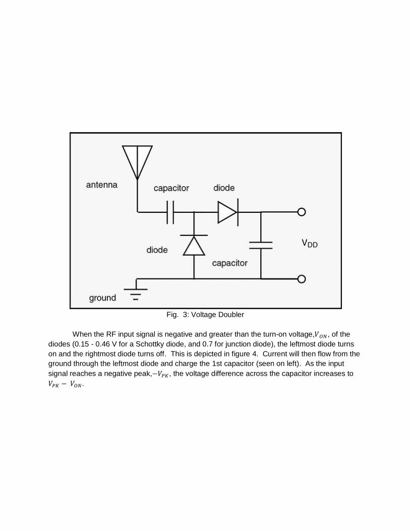
Fig. 3: Voltage Doubler
When the RF input signal is negative and greater than the turn-on voltage, , of the
diodes (0.15 - 0.46 V for a Schottky diode, and 0.7 for junction diode), the leftmost diode turns
on and the rightmost diode turns off. This is depicted in figure 4. Current will then flow from the
ground through the leftmost diode and charge the 1st capacitor (seen on left). As the input
signal reaches a negative peak, , the voltage difference across the capacitor increases to
.

Fig. 4: Voltage Doubler when RF input signal is negative
When the RF signal changes polarity (becomes positive) and VPK is greater than VON, the
leftmost diode turns off and the rightmost diode turns on. The 1st capacitor will begin
discharging and flow through the rightmost diode. The total output voltage presented to the rest
of the IC (load), VDD, is described in equations 1 and 2. VPK is the incoming signal from the
antenna, VPK - VON is the voltage across the leftmost diode as it discharges, and - VON is the
potential drop across the rightmost diode.
Eq. 1
Eq. 2
In figure 5 below, it can be seen in that the output voltage is twice that of the input
voltage. In a typical tag IC, the voltage multiplier consists of many voltage doublers cascaded
together so as to provide a much higher voltage than the amplitude of the received RF signal.
The output voltage can further increase by a constant factor N relative to the number of voltage
doublers provided in the circuit: VDD = 2N(VPK – VON). As the number of stages increases
however, the efficiency of the circuit dramatically falls.

Fig. 5: Voltage Doubler when RF input signal is positive
2.1.2 Voltage Regulator
The voltage regulator is used to keep the voltage from the voltage multiplier stable.
Since the RF signal coming from the reader varies in strength, the converted DC current will
also vary. This will adversely affect the performance of the IC. Typical voltage regulators are
made using a resistor and a Zener diode. Although not all voltage regulators in tag ICs use this
type of schematic, for explanation purposes we will elaborate on this design. A simple diagram
for the voltage regulator is depicted in figure 6. The resistor is in series with the Zener diode
and the diode’s breakdown voltage can vary, but for a low power tag IC, we will assume that the
breakdown voltage is 2.4 V. The important thing to note about Zener diodes is that when they
are reverse biased, as long as the input voltage is greater than the breakdown voltage, the
voltage across the Zener diode will always be equal to the breakdown voltage. The current may
increase when the input voltage increases, but the voltage remains the same. Let us assume
that the input voltage varies around 3 V. An RFID IC will not operate unless it gets a current of
at least 10 µA. With this information we can calculate the value of the resistor in equation 3.
We will initially use a current of 60 µA to determine the resistance.
Eq. 3
Now let’s see what happens when the voltage varies between 2.5 and 3.5 V. Keep in
mind that the voltage across the Zener diode will always be 2.4 V but the current will change.

Eq. 4
Eq. 5
Despite the change in the input voltage, the output voltage stays at 2.4 V and the current
is still enough to power the IC.
Fig. 6: Voltage Regulator
2.1.3 Demodulator
The type of demodulation our tag uses is ASK demodulation. In general, RFID tags can
use ASK or PSK demodulation depending on the reader. Figure 7 shows the CMOS schematic
of the ASK demodulator. The demodulator consists of an envelope detector, a low pass filter,
an average detector, and a comparator. In figure 8 you can see an example of an ASK
modulated RF input signal along with its demodulated waveform.
Figure 8 shows an example of a typical envelope detector. The envelope detector takes
the RF signal sent by the reader and provides an output which tracks the envelope of the
message signal. The diode turns on and the capacitor stores up the charge on the positive
cycle of the input signal. When the input signal falls below its peak value, the diode will turn off
(open) because the voltage stored at the capacitor will be greater than the input signal voltage.
As a result, the capacitor will begin to slowly discharge through the resistor. This process
repeats when the input signal is on the positive half of the cycle. The rate at which the
capacitor charges and discharges, given the input signal contains a 915 MHz carrier, is known
as the time constant, and is described in equation 6 below.

Eq. 6
The time constant, RC, must be far less than , the signal period of the incoming signal,
in order to maintain its integrity and to also filter out the high-frequency carrier. The average
detector is used to track the average of the incoming signal. The, the comparator outputs the
message signal by comparing the output of the envelope detector with the average value of the
message signal.
Fig. 7: ASK Demodulator
Fig. 8: Envelope Detector
2.1.4 Clock Generator
The purpose of the clock generator is to provide a stable clock signal for the signal
processing block and modulator. It takes the demodulated signal as its input and outputs the
clocked signal to the digital logic. The clock generator consists of two parts, an oscillator and a
3-bit counter (figure 9). The oscillator produces a signal at the data bit rate ranging from 40 -
640 kHz depending on what the reader requests. The 3-bit counter takes the two inputs from
the oscillator and the demodulated ASK signal and determines where to output the clock signal.
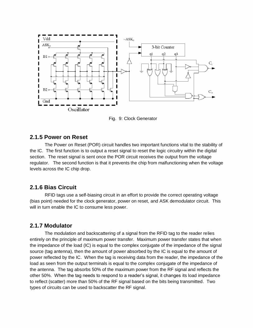
Fig. 9: Clock Generator
2.1.5 Power on Reset
The Power on Reset (POR) circuit handles two important functions vital to the stability of
the IC. The first function is to output a reset signal to reset the logic circuitry within the digital
section. The reset signal is sent once the POR circuit receives the output from the voltage
regulator. The second function is that it prevents the chip from malfunctioning when the voltage
levels across the IC chip drop.
2.1.6 Bias Circuit
RFID tags use a self-biasing circuit in an effort to provide the correct operating voltage
(bias point) needed for the clock generator, power on reset, and ASK demodulator circuit. This
will in turn enable the IC to consume less power.
2.1.7 Modulator
The modulation and backscattering of a signal from the RFID tag to the reader relies
entirely on the principle of maximum power transfer. Maximum power transfer states that when
the impedance of the load (IC) is equal to the complex conjugate of the impedance of the signal
source (tag antenna), then the amount of power absorbed by the IC is equal to the amount of
power reflected by the IC. When the tag is receiving data from the reader, the impedance of the
load as seen from the output terminals is equal to the complex conjugate of the impedance of
the antenna. The tag absorbs 50% of the maximum power from the RF signal and reflects the
other 50%. When the tag needs to respond to a reader’s signal, it changes its load impedance
to reflect (scatter) more than 50% of the RF signal based on the bits being transmitted. Two
types of circuits can be used to backscatter the RF signal.

Fig.10: Backscatter using Open Circuit
The first circuit is shown in figure 10. It utilizes an open circuit in parallel with the load
resistance. This circuit is a simplified representation and only includes the real part of the
impedance whereas in a true IC, there would be a real and a complex part. In the circuit
diagram, represents the resistance produced in the antenna when current flows through it.
Rload represents the resistance of the IC as seen from the antenna. State 1 represents the
default state for the RFID tag. When the tag is in state 1, the power scattered by the antenna is
equal to the product of the current squared and the resistance. The current flowing through the
load resistor can be calculated from Ohm’s law.
Eq. 7
We can then determine the power delivered to load in the default state. In the default
state, the load resistance is equal to the resistance from the antenna to achieve maximum
power transfer. The power then delivered to the load and scattered back through the antenna is
given in equation 8. This corresponds to the power delivered to the unmodulated antenna.
Eq. 8
When the tag is in state 2 there is no current flowing through the IC so zero power is
delivered to the load and therefore no power is backscattered. The change in backscattered
signal power corresponds to an ASK modulated signal where the amplitude of the signal
changes relative to what bits are being sent.
During the process of modulation, the tag switches between states 1 and 2 in order to
backscatter a signal of changing amplitude. In MMS encoding, the number of tag state
transitions that occur within a cycle time determine what bit was sent. If a logical “0” is sent,
then there will not be any state changes in the signal regardless of whether the state is 1 or 2. If
a logical “1” is sent, there will be 1 state change regardless of whether it changes from state 1 to
2 or 2 to 1. In MMS encoding, the tag switches symmetrically between states 1 and 2. This
means that the tag will spend half of the modulation time in state 1 and the other half in state 2.
The power that is backscattered from the tag is due to the change in current between the
modulated and unmodulated states. The average backscattered power is then equal to half the
peak power found in equation 8. The power delivered to the IC during modulation is then equal
to the backscattered power.
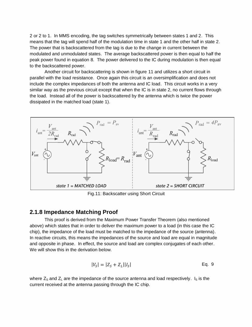
Another circuit for backscattering is shown in figure 11 and utilizes a short circuit in
parallel with the load resistance. Once again this circuit is an oversimplification and does not
include the complex impedances of both the antenna and IC load. This circuit works in a very
similar way as the previous circuit except that when the IC is in state 2, no current flows through
the load. Instead all of the power is backscattered by the antenna which is twice the power
dissipated in the matched load (state 1).
Fig.11: Backscatter using Short Circuit
2.1.8 Impedance Matching Proof
This proof is derived from the Maximum Power Transfer Theorem (also mentioned
above) which states that in order to deliver the maximum power to a load (in this case the IC
chip), the impedance of the load must be matched to the impedance of the source (antenna).
In reactive circuits, this means the impedances of the source and load are equal in magnitude
and opposite in phase. In effect, the source and load are complex conjugates of each other.
We will show this in the derivation below.
Eq. 9
where ZS and ZL are the impedance of the source antenna and load respectively. IS is the
current received at the antenna passing through the IC chip.

Eq. 10
Equation 11 describes the power delivered to the load. We want to find the real and imaginary
parts of ZL so as to maximize this power delivered.
Eq. 11
where RS and XS are the real and imaginary parts, respectively, of the impedance ZS, and RL
and XL are the real and imaginary parts, respectively, of impedance ZL.
Since we want the power delivered to the load to be a maximum, we want the
denominator of the equation above to be as small as possible. We can do this by setting
XL = -XS. This leaves us with:
Eq. 12
Now, we can find the value for RL that will maximize equation 12 by differentiating the
denominator with respect to RL and setting it equal to zero.
Eq. 13
Now solving for RL, we find that RL = RS. We have therefore shown that the real part of
the impedance is equal in magnitude and opposite in phase when the power transferred to the
IC chip is a maximum.
2.1.9 Backscattered Subcarrier Modulation
As stated in section 2.1.7, the RFID tag changes its impedance in order to reflect a
different amount of power corresponding to the message signal. An important thing to note that
was not mentioned in the previous section is that the RFID tag does not backscatter the binary
message signal. It backscatters an ASK modulated message signal. This means that the final
backscattered signal will have been amplitude modulated twice from its original baseband
message signal. The first carrier signal is a sequence of alternating 1’s and 0’s set at the RFID
reader uplink frequency. The uplink frequency of the RFID reader used in our project is 40 kHz.
This ASK modulated signal at carrier frequency 40 kHz is then ASK modulated a second time at
the carrier frequency of the continuous wave being transmitted from the RFID reader. The CW

frequency in our project is 915 MHz. This is the result of Miller Modulated Subcarrier (MMS)
encoding.
MMS encoding takes the baseband signal and multiples it by a series of alternating 1’s
and 0’s with a frequency of 40 kHz. The baseband signal is itself encoded by varying the
number of state changes of the transmitted bit corresponding to a “1” or a “0”. The tag state has
a change in the beginning and end of every clock cycle. For every binary “1” there is an
additional state change in the middle of the cycle whereas for a “0” there is no additional state
change. There are three different ways to use MMS encoding. Each way involves changing the
data rate of the ASK modulated signal. The different types of MMS encoding are depicted in
Figure 12.
Fig. 12: Miller Modulated Subcarrier signals
The backscattered signal is a sum of two sinusoidal signals (s1(t) and s2(t)) each at a
frequency of 40 kHz away from the original CW carrier frequency. The backscattered signal s(t)
is described in equation 14. A1 and A2 are the amplitude of the sidebands and fs is the
frequency of the subcarrier which is 40 kHz.
Eq. 14
The specific reason for using MMS encoding along with subcarrier modulation is
explained in section 2.2.2 on the RFID reader receiver.
2.1.10 Signal Processing Unit

The signal processing unit’s main components are the controller and the memory unit.
The function of the controller is to receive the demodulated signal from the demodulator and the
clock signal from the clock generator in order to find the number of pulses needed in one cycle
to generate the incoming signal. The controller then responds appropriately depending on the
instructions provided by the instruction register. For example, the controller may need to fetch
data, which will be stored in the memory unit that needs to be transmitted back to the reader
(i.e. random 16-bit number or EPC number). It may also need to write data to memory. The
second important function of the controller is to send a “wake up” call to make sure that the tag
is on.
2.2 RFID Reader
An RFID reader is essentially a radio transceiver. It transmits a modulated signal at a
particular carrier frequency, and then receives and demodulates a response. One of the few
distinctions of a passive RFID reader is that aside from transmitting a modulated signal at the
carrier frequency, the reader always transmits a continuous wave at the carrier frequency to
provide power to the passive RFID tag. The RFID reader is a full-duplex receiver meaning that
it transmits and receives signals simultaneously. This full-duplex transceiver, however, is
different than most full-duplex devices like cell phones because it can transmit and receives
signals at the same carrier frequency. We will discuss in detail how a RFID reader works by
first explaining the transmitter side and then explaining the receiver side. Figure 14 depicts a
full duplex system where the transmitter antenna transmits a CW to the tag and the tag
backscatters the response to the receiver antenna. The important thing to note is that the
receiver not only receives the backscattered signal from the tag but also the transmitted CW
from the transmitter. The CW has much higher amplitude than the backscattered signal so the
receiver has the task of differentiating the backscattered signal from the CW.
Fig. 13: Full Duplex RFID System

2.2.1 Transmitter
The RFID transmitter is much simpler than the RFID receiver. It’s main goal is to send
the ASK modulated messages to the tag and then in between the messages, send a continuous
915 MHZ (adjustable) wave to allow the tag to back-scatter the signal and send data back to the
receiver. We can represent the transmitter in Figure 14 as a 915 MHz oscillator, two amplifiers,
and a transmitting antenna. The messages are amplitude modulated by varying the DC power
supplied to the second output amplifier. A logical “1” is sent with maximum DC power supplied
to the second output amplifier and a logical “0” is send with the minimum DC power supplied to
the second output amplifier. All RFID readers use some sort of encoding scheme to transmit
data, but we will not go into any further explanation on that topic. When the CW is being sent,
the DC power to the output amplifier is left constant. In this transmitter, only the amplitude of
the transmitted signal is altered and not the phase, although other RFID reader designs are able
to send phase modulated signals.
Fig. 14: RFID reader transmitter and modulated signal frequency response.
2.2.2 Receiver
The main challenge of the receiver is to differentiate the backscattered signal from the
CW despite the fact that the CW is at a significantly higher power level than the backscattered
signal. The answer to this challenge lies in the backscattered modulation technique described
in section 2.1.9. The backscattered signal is subcarrier modulated so that it is received at a
frequency offset compared to the CW signal. Equation 14 in section 2.1.9 depicted the
backscattered signal. The signal entering the antenna at the receiver is a combination of the
backscattered signal and reflections of the transmitted CW. Since the transmitter radiates the
CW outwards, multiple paths of the signal are able to reach the receiver antenna. This is
depicted in equation 15. We will denote r(t) as the signal seen at the receiver antenna. AC is
the amplitude of the CW signal and θ is the phase shift of the CW signal. Note that there are n
CW signals received by the antenna all at a different amplitude and phase shift.

Eq. 15
For future purposes we will lump all of the CW signals received at the receiver antenna
as n(t) as described below in equation 16.
Eq. 16
Equation 15 can then be written as the follows in equation 17. The resulting signal can
then be seen graphically in figure 15. The CW from the transmitter is depicted as an impulse at
the carrier frequency and the backscattered signals are shown at their frequency offsets.
Eq. 17
Fig. 15: Frequency spectrum of signal at receiver
The next step would be to remove the CW reflections from the transmitter would be to
use a band pass filter surrounding one of the backscattered sidebands. This, however, would
be very difficult and costly because narrow band pass filters in the 900 MHz range are not
cheap. The easiest thing to do is down convert the signals to baseband and then use a filter to
remove the CW component. This is achieved using a homodyne receiver structure as shown in
figure 16.
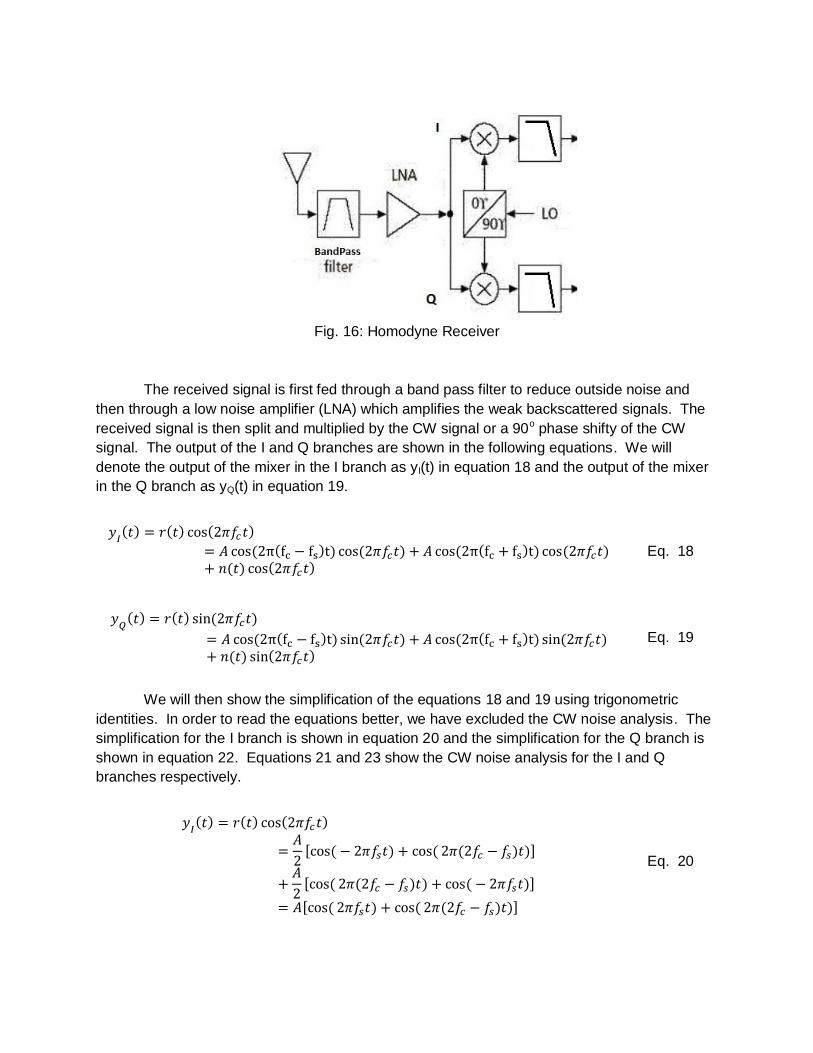
Fig. 16: Homodyne Receiver
The received signal is first fed through a band pass filter to reduce outside noise and
then through a low noise amplifier (LNA) which amplifies the weak backscattered signals. The
received signal is then split and multiplied by the CW signal or a 90o phase shifty of the CW
signal. The output of the I and Q branches are shown in the following equations. We will
denote the output of the mixer in the I branch as yI(t) in equation 18 and the output of the mixer
in the Q branch as yQ(t) in equation 19.
Eq. 18
Eq. 19
We will then show the simplification of the equations 18 and 19 using trigonometric
identities. In order to read the equations better, we have excluded the CW noise analysis. The
simplification for the I branch is shown in equation 20 and the simplification for the Q branch is
shown in equation 22. Equations 21 and 23 show the CW noise analysis for the I and Q
branches respectively.
Eq. 20
Eq. 21
Eq. 22
Eq. 23
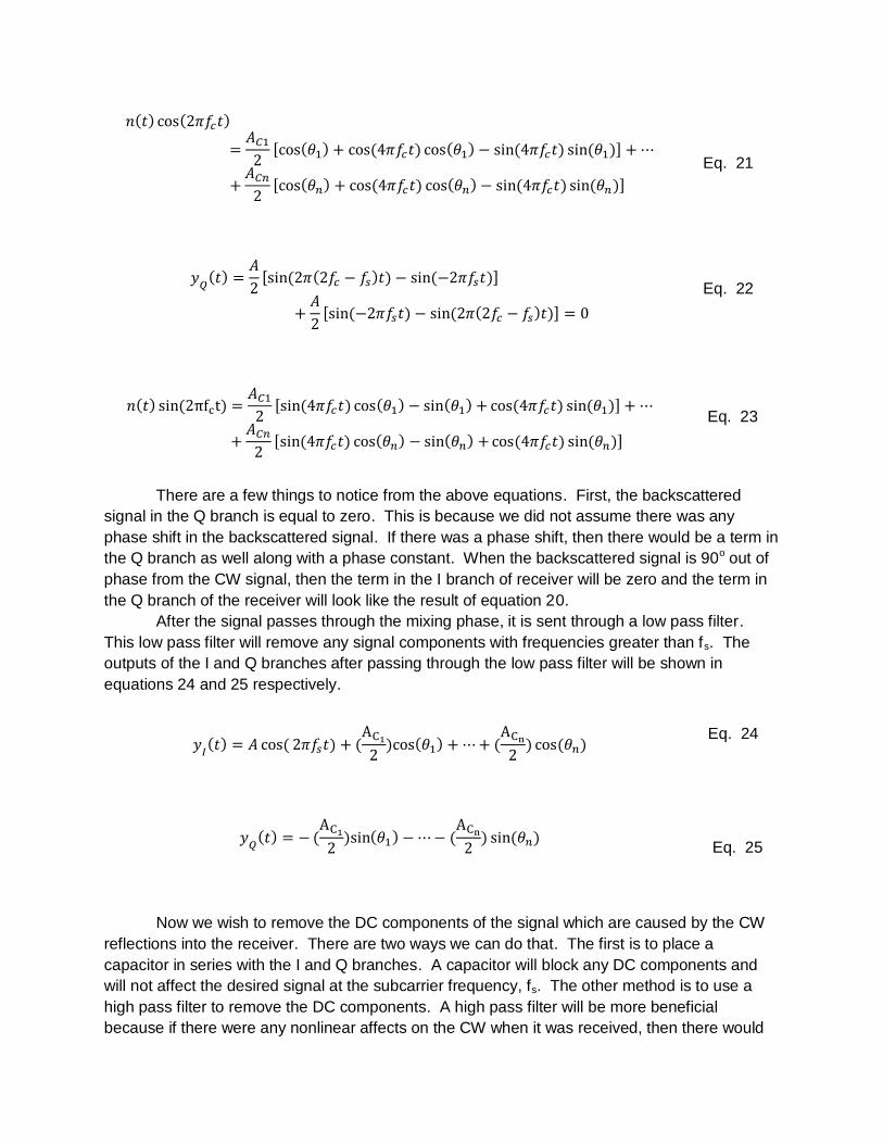
There are a few things to notice from the above equations. First, the backscattered
signal in the Q branch is equal to zero. This is because we did not assume there was any
phase shift in the backscattered signal. If there was a phase shift, then there would be a term in
the Q branch as well along with a phase constant. When the backscattered signal is 90o out of
phase from the CW signal, then the term in the I branch of receiver will be zero and the term in
the Q branch of the receiver will look like the result of equation 20.
After the signal passes through the mixing phase, it is sent through a low pass filter.
This low pass filter will remove any signal components with frequencies greater than fs. The
outputs of the I and Q branches after passing through the low pass filter will be shown in
equations 24 and 25 respectively.
Eq. 24
Eq. 25
Now we wish to remove the DC components of the signal which are caused by the CW
reflections into the receiver. There are two ways we can do that. The first is to place a
capacitor in series with the I and Q branches. A capacitor will block any DC components and
will not affect the desired signal at the subcarrier frequency, fs. The other method is to use a
high pass filter to remove the DC components. A high pass filter will be more beneficial
because if there were any nonlinear affects on the CW when it was received, then there would

be CW noise present at frequencies higher than or lower than DC. The high pass filter would
not remove these frequency fluctuations, but it would reduce them more so than the capacitor
would. After the filtering phase, the I and Q branches are squared and then added together to
produce the final received signal. Equation 26 shows the received backscattered signal. Note
that it is a squared version of the actual backscattered signal. This is due to the I and Q
separations. This is used to allow for a backscattered signal to be received with a phase
difference then the CW signal.
Eq. 26
Probability of Error
We will now determine the probability of error for the received signal once passes
through figure 16. We will assume that the DC components from the CW were filtered out and
all that remains is the backscattered signal and white Gaussian noise. We can split up the
decoded signal into a possibility of two signals depending on whether a “1” or a “0” was sent.
We will denote the received signal as y(t) and n(t) as the white Gaussian noise and it is shown
in equation 27.
Eq. 27
The signal will then pass through a matched filter to maximize the SNR. After passing
through the matched filter, the signal will be sampled at rate of t = T. We will denote the output
of the sampler as x(T) and it is depicted in equation 28.
Eq. 28
The probability of error is the probability that a “1” is detected when a “0” was sent plus
the probability that a “0” is detected when a “1” was sent. We will assume the probability of
sending a “1” or a “0” is ½. This is depicted in equation 29.
Eq. 29
To determine the probability that we decode a “1” when a “0” was sent we will use
equation 28. The output of the sampler can be split up into a sum of two convolutions. The first
convolution is between the backscattered signal s(t) and the matched filter and the second is
between the white Gaussian noise and the matched filter. Equation 30 shows a further
simplification of equation 28 . In the equation we removed the matched filter and replaced it
with s(T-τ) because we will chose the matched filter to be the time reversed representation of
the backscattered signal.

Eq. 30
To proceed any further we must elaborate on equation 30. The right part of the equation
is a Gaussian random variable. The left side of the equation reduces down to a number. We
can therefore characterize the signal x(T) as a Gaussian random variable with a mean of Γ (we
will assume that the white Gaussian noise, n(t), is of mean 0). We then need to figure out the
variance of the Gaussian signal to determine the probability of error. Equation 31 depicts the
variance of the Gaussian signal. T denotes the period of the bit being transmitted.
Eq. 31
Before we can finish determining the probability of error for the system, we need to take
a look at the signal to noise ratio for the Gaussian signal out of the sampler. The signal in this
case is the left side of equation 30 and the noise is the standard deviation of equation 31. This
is shown in equation 32.
Eq. 32
To simplify this equation we can use the Cauchy Schwarz inequality. This will simplify
equation 32 into equation 33.
Eq. 33
This means that the signal to noise ratio only depends on the energy of the signal being
transmitted. We can determine the energy in the backscattered signal based on our definition of
the Miller modulated subcarrier encoding described in section 2.1.9. In that type of encoding, a
logical “0” is sent with energy A2 and a logical “1” is sent with energy A2/2. With this we can
show the probability density function of the received signal and then describe it in equation form.
Figure 17 depicts the probability density function for the received random variable X.

Fig. 17: Probability Density Function for Gaussian Random Variable X
The probability density functions are then shown below in equations 34 and 35.
Eq. 34
Eq. 35
The previous two equations denoted the probability density functions. The probability of
error is the area under the curves in figure 17 where the two density functions overlap. The final
probability of error is depicted in equation 36.
Eq. 36
Dynamic Range
When the CW is transmitted from the RFID reader, some objects in the environment
reflect the CW and is picked up by the receiver. These unwanted “echoes” are clutter noise and
could potentially interfere with the subcarrier frequency of the desired backscattered signal. The
clutter noise may be picked up by the receiver with such high power that it saturates the
receiver and prevents detection of tag response. This can be prevented if the receiver has a

large dynamic range. Dynamic range of a receiver, usually expressed in decibels, is defined as
a ratio of the maximum to the minimum signal input power levels over which the receiver can
operate with some specified performance. The maximum signal level might be set by the
nonlinear effects of the receiver response that can be tolerated, and the minimum signal may be
the desired backscattered signal. If the receiver’s dynamic range is small, then a relatively
strong “echo” can cause the receiver to saturate. Some of the more important characteristics of
the receiver’s dynamic range are described below.
Receiver Input Noise Level
It is very important to understand and specify the noise level at the receiver input. This
is set by the antenna noise temperature and its total effective noise gain or loss. The noise
level can be specified either as an RMS power in a specified bandwidth or as a noise power
spectral density.
System Noise
The system noise consists of both the antenna and receiver noise. Usually with RFID
systems, the receiver input noise exceeds that of the noise due to the receiver itself. This
proves that the receiver has only a small impact on the system noise temperature. It is very
important while defining dynamic range parameters such as signal to noise ratio to specify
whether the noise is the receiver noise or the system noise.
Spurious Free Dynamic Range (SFDR)
The ratio of the maximum signal level to that of the largest spurious signal created within
the receiver is called SFDR. This parameter is determined by a variety of factors such as the
mixer intermodulation spurious, the spurious content of the receiver local oscillators, the
performance of Analog to Digital converter, and the paths that many result in unwanted signals
coupling onto the receiver signal path. An ideal mixer acts as a multiplier that produces an
output proportional to the product of the two input signals. In passive mixers, the modulation is
performed using Schottky barrier diodes where increased dynamic range is required. What
happens is that the input RF signal at fR is modulated by the LO signal fL. The resulting output
signal frequencies [fR+fL and fL-fR] are the sum and difference of the two input frequencies. All
mixers produce unwanted intermodulation spurious responses with frequencies ,
and the degree to which these spurious precuts impact the RFID performance depends upon
the type of mixer and overall RFID performance requirements.
Clutter Noise
As mentioned above, the receiver picks up the backscattered signal in addition to
unwanted reflected signals. The reflected signals are actually the transmitted signal that gets
reflected by its surroundings (these reflected signals are also known as clutter). These
reflections carry power that will also be picked up by the receiver. The problem with this is that
the sidebands of the clutter noise can potentially spillover into the frequency range of interest.
The phase of the sidebands of the clutter is related to each other and the carrier by either
amplitude or frequency modulation. AM components are generally much lower in power than
the FM components, and less problematic. As such, we will discuss the complications of the

FM components. Let’s take as the modulating frequency in the noise sidebands and ∆f to be
maximum frequency deviation. Then the peak amplitude of the carrier and the nearest noise
sidebands can be described by equations 37 and 38, respectively, using the Bessel function
Eq. 37
Eq. 38
The modulation index β =
.
The Bessel functions can then be approximated given that the modulation index is small. This
simplifies the equations shown above to the equations 39 and 40.
Eq. 39
Eq. 40
We can now find the ratio of the power in the nearest sidebands to that of the carrier. This will
be
Eq. 41
Our RFID reader is implemented using bi-static antennas greatly reduces the spillover
and clutter effects.
Interference Canceling
There is one method that is used in some RFID readers to reduce the unwanted signals
produced by the transmitter. The method is called interference cancelling and is a dynamic
method that mixes the received signal with a CW that is phase shifted to cancel out the received
CW signal. The idea is that if the received CW signal is multiplied by a signal that is orthogonal
to it and then integrated, the CW noise will be effectively removed from the received signal. The
problem lies in not knowing exactly what signal to multiply the received signal by to remove this
CW noise. One method is to first multiply the received signal by a 90o phase shifted CW signal
and then measure the amount of CW noise present after the integration process. The multiplied
signal is then continuously adjusted (either in its phase, frequency, or amplitude) to further
reduce the CW noise. It is an iterative process that continuously measures the amount of noise
present and then changes parameters to try and further reduce the noise.
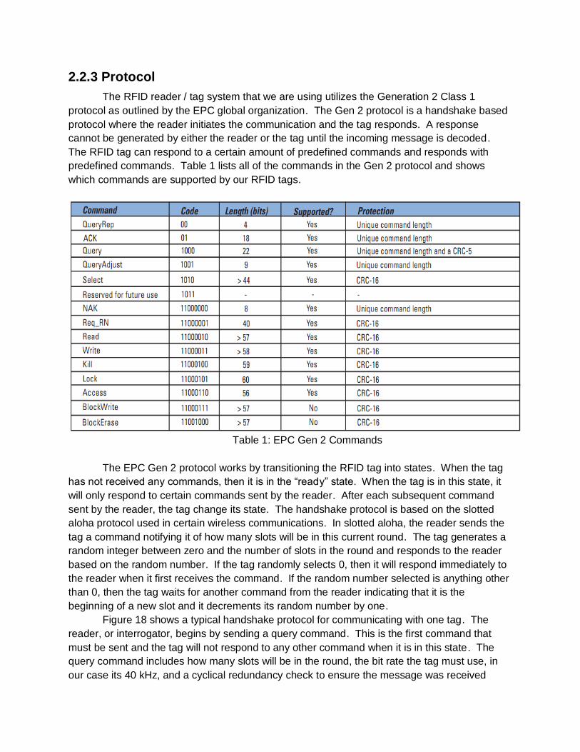
2.2.3 Protocol
The RFID reader / tag system that we are using utilizes the Generation 2 Class 1
protocol as outlined by the EPC global organization. The Gen 2 protocol is a handshake based
protocol where the reader initiates the communication and the tag responds. A response
cannot be generated by either the reader or the tag until the incoming message is decoded.
The RFID tag can respond to a certain amount of predefined commands and responds with
predefined commands. Table 1 lists all of the commands in the Gen 2 protocol and shows
which commands are supported by our RFID tags.
Table 1: EPC Gen 2 Commands
The EPC Gen 2 protocol works by transitioning the RFID tag into states. When the tag
has not received any commands, then it is in the “ready” state. When the tag is in this state, it
will only respond to certain commands sent by the reader. After each subsequent command
sent by the reader, the tag change its state. The handshake protocol is based on the slotted
aloha protocol used in certain wireless communications. In slotted aloha, the reader sends the
tag a command notifying it of how many slots will be in this current round. The tag generates a
random integer between zero and the number of slots in the round and responds to the reader
based on the random number. If the tag randomly selects 0, then it will respond immediately to
the reader when it first receives the command. If the random number selected is anything other
than 0, then the tag waits for another command from the reader indicating that it is the
beginning of a new slot and it decrements its random number by one.
Figure 18 shows a typical handshake protocol for communicating with one tag. The
reader, or interrogator, begins by sending a query command. This is the first command that
must be sent and the tag will not respond to any other command when it is in this state. The
query command includes how many slots will be in the round, the bit rate the tag must use, in
our case its 40 kHz, and a cyclical redundancy check to ensure the message was received

without error. The tag will respond if it received the query without error and if it randomly
selected slot 0. The tag responds with a RN16, a 16 bit random number that differentiates it
from any other tag within range. The reader will then respond with an ACK that includes the
RN16 number sent by the tag. If the tag receives the ACK with the correct RN16 number, it will
backscatter its EPC number which is a 96 bit number that identifies the tag. When the reader
receives the EPC number, it could refrain from sending any more commands to the tag or send
additional commands to write data to the tag if necessary.
Fig. 18: Handshake Protocol for EPC Gen 2
3. Procedure
3.1 Initial Procurement and Installation
Since we did not have access to a commercial RFID reader, we did some research into
how we can build our own RFID reader. Upon doing research, we realized we could use GNU
Radio to implement an RFID reader. GNU Radio is open source software that performs
communications processing at the software level, instead of at the hardware level. It is defined
by signal processing blocks and flow graphs. Each block handles a specific signal processing
operation (i.e. filtering), and graphs call these blocks, set their parameters, and connect them
together. Next, we researched the Universal Software Radio Peripheral (USRP), which is
essentially an RF front end used to transform the RF signals designed in software to the real
world.
The next steps involved configuring and installing GNU Radio and USRP. We found that
GNU Radio operates easily and is supported by Linux operating systems. So we installed
Ubuntu on a laptop and started the dissection of the GNU Radio code.
We focused our attention next on making an RFID reader. While we were researching
this topic, we came across the work of a PhD student, Michael Buettner from Washington
University, who had designed an RFID reader using GNU Radio and USRP. We installed this
code and began implementing the necessary changes. This task itself took majority of our time
due to the fact that we had to first understand what the purpose of each file was and understand
the code. The Appendix provides the exact steps that we took to install and configure the
USRP, GNU Radio, and RFID code.
3.2 Testing / Adjustments
Initially, when we started the testing, our RFID reader did not detect the presence of any
tags. Using the software plotting tool, Octave, we were able to see if the reader received any
modulated back-scatter signal from the tags. We initially bought Gen 2 Inlays from TI which
were not be detected by the RFID reader. Upon further research we found out that the tags
were outdated and discontinued. Therefore, we bought Alien Omni-Squiggle Sticker Labels,
which we referred to us by Michael Buettner, as these were the tags he originally tested his
RFID reader. The new RFID tags gave us the result we expected as we were able to detect the
RFID tag.
For us to properly test the device, we made a pair of stands (using PVC pipes) for our
antennas which we taped to a cardboard box and cut a hole out in the center so as to slip the
box through the individual stands. Then we took a rotating chair and taped the tag on the back
and tested the distance of which a tag can be read. Since the antennas we are using have a
beam-width of 40º we took string and measured out the angle from the center of the antenna.
We then moved the chair around and ran the device and came to a conclusion that the tag can
only be read from 9 inches away within the 40º width. We had to go back to the code and
adjust the amplitude of the transmitting signal to realize that the best fit was 27,000 at 915 MHz.
Refer to the section labeled Pictures to view our setup.
3.3 Code Modifications
When we first started testing the Alien Omni-Squiggle Sticker Labels we noticed that all
of the tags had the same pre programmed EPC code on them. This made it impossible to test
the RFID reader with multiple tags within range because we were not be able to distinguish one
tag from another. Our solution was to program the tags ourselves using our RFID reader. As
shown in table 1 in the RFID theory section of the report, the RFID tags can respond to a write
command, and we then can program there non volatile memory (NVM) with a new EPC code.
The problem with the solution is that Michael Buettner, the PhD student who wrote the code,
had not seen any value in writing to an RFID tag so had not implemented the code.
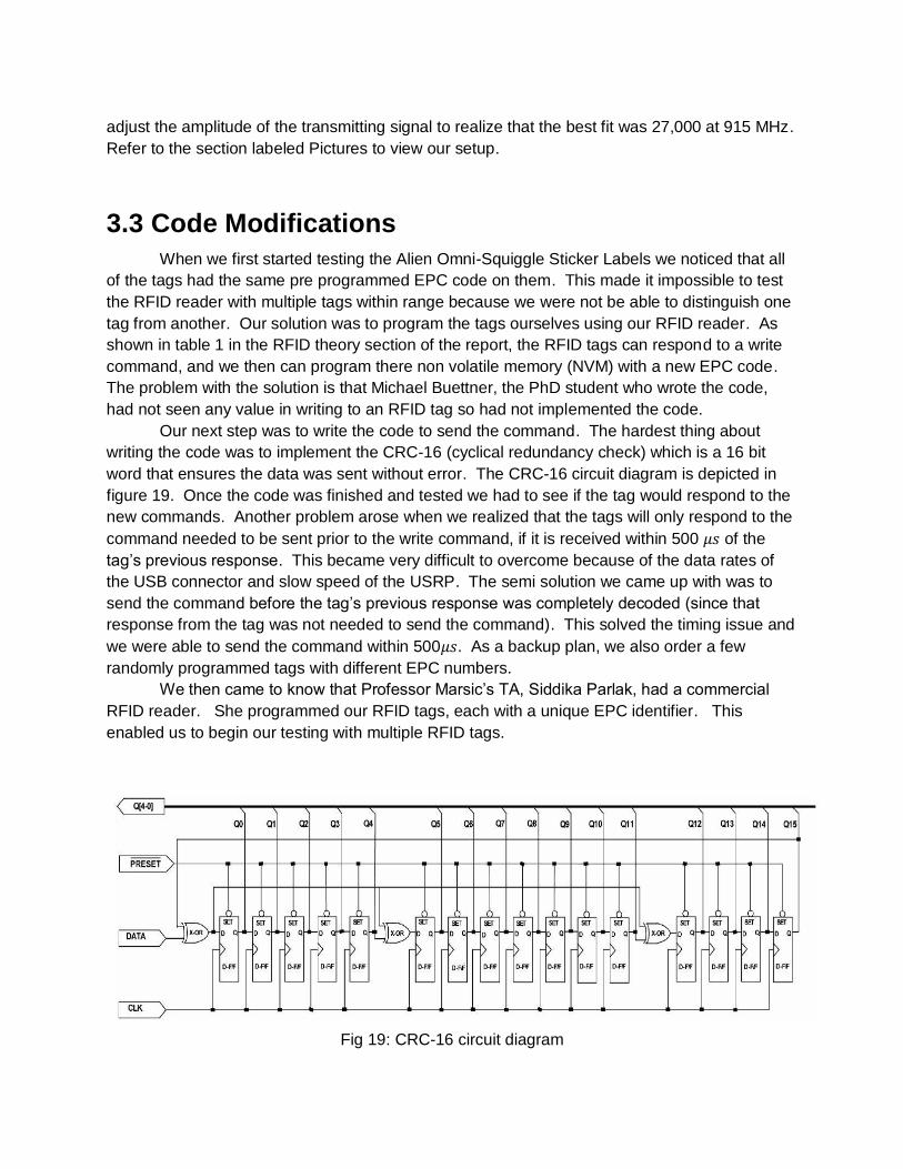
Our next step was to write the code to send the command. The hardest thing about
writing the code was to implement the CRC-16 (cyclical redundancy check) which is a 16 bit
word that ensures the data was sent without error. The CRC-16 circuit diagram is depicted in
figure 19. Once the code was finished and tested we had to see if the tag would respond to the
new commands. Another problem arose when we realized that the tags will only respond to the
command needed to be sent prior to the write command, if it is received within 500 of the
tag’s previous response. This became very difficult to overcome because of the data rates of
the USB connector and slow speed of the USRP. The semi solution we came up with was to
send the command before the tag’s previous response was completely decoded (since that
response from the tag was not needed to send the command). This solved the timing issue and
we were able to send the command within 500 . As a backup plan, we also order a few
randomly programmed tags with different EPC numbers.
We then came to know that Professor Marsic’s TA, Siddika Parlak, had a commercial
RFID reader. She programmed our RFID tags, each with a unique EPC identifier. This
enabled us to begin our testing with multiple RFID tags.
Fig 19: CRC-16 circuit diagram

3.4 GUI Application
In our approach in making a GUI Application, we had two things that we wanted to
tackle. One was to integrate the RFID reader with the application and the other was to make a
user friendly application so our users would not have difficulty navigating through it. The setup
of our application is set so the user selects a product from a drop down box. Initially, the user
would have to manually input what products they want the RFID reader to track, and also assign
it with the appropriate tag (text file). When a product is selected by the user, if the EPC number
is detected in the log_out file of the RFID reader, then the EPC, Purchased date, and the time of
detection will appear in the appropriate fields. Along with that, there is a field called availability
that would be filled saying “Available.” In the case where the EPC has not been detected, the
availability field will be set to “Not Available” and you will see the EPC fie ld and Purchased date
empty so there is no confusion. The application also allows the user to update / change the
purchased date of the individual product by using an option on the application called “Update
Date Purchased.” We also have a clear button which can clear all the fields.
A separate text file is created so the user can initially put in the products and given EPC
number. Our algorithm compares each EPC number in the text field to the EPC number in the
log_out file that has been last updated. Since the log_out file does not delete itself after every
scan and logs underneath the previous scan, we had to make sure our application only reads
the “latest” scan instead a previous scan. We wrote an algorithm that reads the file from the
bottom up and stops when it hits a particular string that indicates a scan has been started. Then
it reads that particular block of data and scans to see if it finds a match with the EPC number
from the text file. Our algorithm also keeps track of the time and day when the RFID reader
runs by checking when the log_out file was last modified. Along with all this, we thought it
would be useful if by a click of a button the application showed a list of products that is
recommended to buy. The list would display all the products not detected by the recent scan.
The simplicity of our application makes it enjoyable for the user to navigate.
4. Technical Specifications
4.1 USRP ● Four high-speed analog-to-digital converters - 64 MS/s at a resolution of 12 bits
● Four high-speed digital-to-analog converters- 128 MS/s at a resolution of 14 bits
● Two digital up converters with programmable interpolation rates
● Two digital down converters with programmable decimation rates
● Capable of processing signal up to 16 MHz wide
● An Altera Cyclone
● A Cypress EZ-USB FX2 high-speed USB 2.0 controller
● 4 extension sockets (2 TX, 2 RX) in order to connect 2-4 daugtherboards
● 64 GPIO pins available through 4 Basic TX/Basic RX daughterboards

4.2 RFID Tags
Alien Omni-Squiggle Sticker Label
Dimensions (W x H mm): 101.6 x 101.6
RFID Chip: Monza
Air Interface: EPC Class 1 Gen 2
EPC Memory: 96-bits
Read Range: 3-5 meters
Gen 2 Inlay
Dimensions (W x H mm): 95.25 x 38.1
Air Interface: EPC Class 1 Gen 2
User Memory: 96-bits
Operating Frequency: 860-960 MHz
Data sheet: http://www.ti.com/rfid/docs/manuals/pdfSpecs/epc_inlay.pdf
Read Range: 3-5 meters
4.3 Antenna
Alien Antenna
Frequency Range: 860-930 MHz
Polarization: Circular
3dB Beam-width: 40º nominal
Return Loss: -15dB across frequency range

5. Cost Analysis & Comparison
In order for a project to be truly successful, it must ultimately be economically feasible,
and be marketable to a larger audience (e.g. the one in question for this project is the everyday
user). Shown below is a table outlining the necessary parts ordered and its associated costs.
Item Quantity Cost
Universal Software Radio Peripheral (USRP) 1 $700.00
RFX900 Daughterboard 2 $550.00
Alien RFID Circular Antenna 2 $363.98
RFID Gen 2 Inlay 25 $21.75
Alien Omni-Squiggle Sticker Label 10 $12
Shipping and Handling $60
Stands 2 $67
Total Cost: $1774.73
The UHF RFID tags are relatively inexpensive, which is important considering there can
be many food products that a person may need to track within his/her refrigerator. However,
the combination of the cost of the USRP, daughterboards, and antennas is a steep one.
Implementation of this system in the real world would maintain a fixed cost of $1613.98
(includes USRP, daughterboard, and antennas). The variable cost in this would be the RFID
tags. The number of tags bought by the user depends on his or her needs, and these needs
vary from person to person. As such, it is questionable as to whether or not this product could
provide revenues if made available to the public.
Commercial Gen 2 RFID Reader
A commercial Gen 2 RFID Reader as seen below is roughly $1500. The specifications
to this RFID is similar to the RFID we built using the USRP, RFX900 Daughterboard, and GNU
Radio. The main difference lies in the fact that this commercial reader supports more LAN
protocols and uses monostatic antennas. Commercial readers generally have hardware to
isolate the receive chain from the CW signal, use sharp cut-off filters to suppress all but the tag
response, and transmit at a higher power. Using the USRP and GNU Radio gives a high
degree of flexibility with respect to both the MAC and PHY layers of the system. The level
flexibility is only possible with this setup and not with commercial readers which allows low-level
RFID research.
6. Conclusion The implementation of the RFID reader using GNU Radio and USRP was successful,
but difficult. We were successfully able to read multiple RFID tags, and design a Java
application to recommend the user to buy food products based upon availability. Our main
difficulties included learning how to use Linux, GNU Radio, and USRP. In addition, we had to
make changes to the RFID code to enable reading and writing of the tags. The main drawbacks
of the RFID reader was the read range, which was only 9 inches and the large amplitude we
had to use to successfully read the tags at that range. As a result, we believe the
implementation of this system in the real world is not yet practical as the USRP is still in its
developmental stages, and the costs of such a system are expensive. We do, however, believe
that this implementation would be useful for anyone interesting in testing changes to the RFID
system. But as a commercial product, this implementation falls short.
7. Division of Labor We distributed the work in our project as follows.
RFID Reader code configuration / compilation --> Nishit and Eric
RFID testing past and future --> Nishit, Hiran, and Eric
RFID Reader code modifications/enhancements --> Eric
GUI / Application --> Hiran and Nishit
Report --> Nishit, Hiran, and Eric

8. References [1] Wikipedia: The Free Encyclopedia.
<http://en.wikipedia.org/wiki/Envelope_detector>
< http://en.wikipedia.org/wiki/Maximum_power_transfer_theorem>
[2] Daniel M. Dobkin. Elsevier, 2008. The RF in RFID Passive UHF RFID in Practice.
[3] Meng-Lin Hsia, Yu-Sheng Tsai, Oscal T-C. Chen. An UHF Passive RFID Transponder Using A Low-Power Clock Generator without Passive Components. Dept. of Electrical Engineering, National Chung Cheng University. IEEE, 2006. [4] Merrill Skolnik. McGraw-Hill Professional, 2008. Radar Handbook. [5] Merrill Skolnik. McGraw-Hill College, 1980. Introduction to Radar Systems.

9. Pictures
Fig. 20: USRP and Laptop with GNU Radio Fig. 21: 2 Alien Antennas on
stands
Fig. 22: Gen 2 Tags on Chair Fig. 23: Tags 9 inches away from
Receiver

Fig. 24: Default View of GUI Application
Fig. 25: Drop Down Box of Products

Fig. 26: Display When Product Has Not Been Detected
Fig. 27: Display When Product Has Been Detected
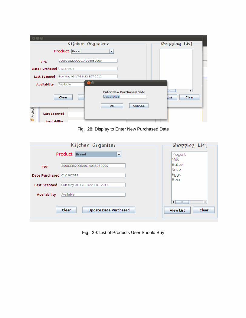
Fig. 28: Display to Enter New Purchased Date
Fig. 29: List of Products User Should Buy

Appendix
1. Install software dependencies for GNU Radio.
● sudo apt-get -y install libfontconfig1-dev libxrender-dev libpulse-dev swig g++
automake autoconf libtool python-dev libfftw3-dev \
● libcppunit-dev libboost-all-dev libusb-dev fort77 sdcc sdcc-libraries \
● libsdl1.2-dev python-wxgtk2.8 git-core guile-1.8-dev \
● libqt4-dev python-numpy ccache python-opengl libgsl0-dev \
● python-cheetah python-lxml doxygen qt4-dev-tools \
● libqwt5-qt4-dev libqwtplot3d-qt4-dev pyqt4-dev-tools python-qwt5-qt4
2. Configure and install GNU Radio
● git clone http://gnuradio.org/git/gnuradio.git
● cd gnuradio
● git branch --track next
● git checkout next
● git branch
● export PKG_CONFIG_PATH=/usr/local/lib/pgkconfig:${PKG_CONFIG_PATH}
● ./bootstrap
● ./configure
● make
● make check
● sudo make install
3. Configure USRP Hardware
● sudo addgroup usrp
● sudo usermod -G usrp -a ece
● echo 'ACTION=="add", BUS=="usb", SYSFS{idVendor}=="fffe",
● SYSFS{idProduct}=="0002", GROUP:="usrp", MODE:="0660"' > tmpfile
● sudo chown root.root tmpfile
● sudo mv tmpfile /etc/udev/rules.d/10-usrp.rules
The open source RFID reader code was downloaded from the following website:
https://cgran.org/wiki/Gen2.
4. Configure, Install, and run RFID reader
● ./configure --prefix=/usr/local/rfid/gnuradio/lib ● make
● sudo make install
● PYTHONPATH=/usr/local/rfid/gnuradio/lib/python2.6/site-packages
GR_SCHEDULER=STS nice -n -20 ./gen2_reader.py