RF front-end for AM/FM DSP car-radio with IF …April 2011 Doc ID 13311 Rev 4 1/61 1 TDA7529 RF...
61
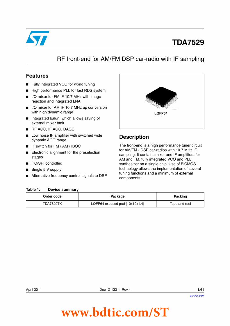
April 2011 Doc ID 13311 Rev 4 1/61 1 TDA7529 RF front-end for AM/FM DSP car-radio with IF sampling Features ■ Fully integrated VCO for world tuning ■ High performance PLL for fast RDS system ■ I/Q mixer for FM IF 10.7 MHz with image rejection and integrated LNA ■ I/Q mixer for AM IF 10.7 MHz up conversion with high dynamic range ■ Integrated balun, which allows saving of external mixer tank ■ RF AGC, IF AGC, DAGC ■ Low noise IF amplifier with switched wide dynamic AGC range ■ IF switch for FM / AM / IBOC ■ Electronic alignment for the preselection stages ■ I 2 C/SPI controlled ■ Single 5 V supply ■ Alternative frequency control signals to DSP Description The front-end is a high performance tuner circuit for AM/FM - DSP car-radios with 10.7 MHz IF sampling. It contains mixer and IF amplifiers for AM and FM, fully integrated VCO and PLL synthesizer on a single chip. Use of BiCMOS technology allows the implementation of several tuning functions and a minimum of external components. LQFP64 Table 1. Device summary Order code Package Packing TDA7529TX LQFP64 exposed pad (10x10x1.4) Tape and reel www.st.com www.bdtic.com/ST
Transcript of RF front-end for AM/FM DSP car-radio with IF …April 2011 Doc ID 13311 Rev 4 1/61 1 TDA7529 RF...
April 2011 Doc ID 13311 Rev 4 1/61
1
TDA7529
RF front-end for AM/FM DSP car-radio with IF sampling
Features■ Fully integrated VCO for world tuning
■ High performance PLL for fast RDS system
■ I/Q mixer for FM IF 10.7 MHz with image rejection and integrated LNA
■ I/Q mixer for AM IF 10.7 MHz up conversion with high dynamic range
■ Integrated balun, which allows saving of external mixer tank
■ RF AGC, IF AGC, DAGC
■ Low noise IF amplifier with switched wide dynamic AGC range
■ IF switch for FM / AM / IBOC
■ Electronic alignment for the preselection stages
■ I2C/SPI controlled
■ Single 5 V supply
■ Alternative frequency control signals to DSP
DescriptionThe front-end is a high performance tuner circuit for AM/FM - DSP car-radios with 10.7 MHz IF sampling. It contains mixer and IF amplifiers for AM and FM, fully integrated VCO and PLL synthesizer on a single chip. Use of BiCMOS technology allows the implementation of several tuning functions and a minimum of external components.
LQFP64
Table 1. Device summary
Order code Package Packing
TDA7529TX LQFP64 exposed pad (10x10x1.4) Tape and reel
www.st.com
www.bdtic.com/ST

Contents TDA7529
2/61 Doc ID 13311 Rev 4
Contents
1 Functional block diagram . . . . . . . . . . . . . . . . . . . . . . . . . . . . . . . . . . . . . 8
2 Pin description . . . . . . . . . . . . . . . . . . . . . . . . . . . . . . . . . . . . . . . . . . . . . 9
3 Function description . . . . . . . . . . . . . . . . . . . . . . . . . . . . . . . . . . . . . . . . 12
3.1 IMR mixer and active balun output . . . . . . . . . . . . . . . . . . . . . . . . . . . . . . 12
3.2 FM RF-AGC . . . . . . . . . . . . . . . . . . . . . . . . . . . . . . . . . . . . . . . . . . . . . . . 12
3.3 AM RF-AGC . . . . . . . . . . . . . . . . . . . . . . . . . . . . . . . . . . . . . . . . . . . . . . . 13
3.4 IF AGC and IF amplifier . . . . . . . . . . . . . . . . . . . . . . . . . . . . . . . . . . . . . . 14
3.5 Dividers . . . . . . . . . . . . . . . . . . . . . . . . . . . . . . . . . . . . . . . . . . . . . . . . . . 14
3.6 D/A converters . . . . . . . . . . . . . . . . . . . . . . . . . . . . . . . . . . . . . . . . . . . . . 14
3.7 VCO . . . . . . . . . . . . . . . . . . . . . . . . . . . . . . . . . . . . . . . . . . . . . . . . . . . . . 15
3.8 FREF . . . . . . . . . . . . . . . . . . . . . . . . . . . . . . . . . . . . . . . . . . . . . . . . . . . . 15
3.9 A/D converter . . . . . . . . . . . . . . . . . . . . . . . . . . . . . . . . . . . . . . . . . . . . . . 15
3.10 GPIO - general purpose IO interface pins . . . . . . . . . . . . . . . . . . . . . . . . 16
3.11 AFSAMPLE/AFHOLD . . . . . . . . . . . . . . . . . . . . . . . . . . . . . . . . . . . . . . . . 17
3.12 Serial bus interface . . . . . . . . . . . . . . . . . . . . . . . . . . . . . . . . . . . . . . . . . . 17
4 Electrical specifications . . . . . . . . . . . . . . . . . . . . . . . . . . . . . . . . . . . . . 19
4.1 Absolute maximum ratings . . . . . . . . . . . . . . . . . . . . . . . . . . . . . . . . . . . . 19
4.2 Thermal data . . . . . . . . . . . . . . . . . . . . . . . . . . . . . . . . . . . . . . . . . . . . . . 19
4.3 General key parameters . . . . . . . . . . . . . . . . . . . . . . . . . . . . . . . . . . . . . . 19
4.4 FM - section . . . . . . . . . . . . . . . . . . . . . . . . . . . . . . . . . . . . . . . . . . . . . . . 20
4.5 AM - section . . . . . . . . . . . . . . . . . . . . . . . . . . . . . . . . . . . . . . . . . . . . . . . 21
4.6 IF - section . . . . . . . . . . . . . . . . . . . . . . . . . . . . . . . . . . . . . . . . . . . . . . . . 22
4.7 VCO . . . . . . . . . . . . . . . . . . . . . . . . . . . . . . . . . . . . . . . . . . . . . . . . . . . . . 24
4.8 Reference frequency input buffer . . . . . . . . . . . . . . . . . . . . . . . . . . . . . . . 24
4.9 Dividers . . . . . . . . . . . . . . . . . . . . . . . . . . . . . . . . . . . . . . . . . . . . . . . . . . 24
4.10 Phase locked loop . . . . . . . . . . . . . . . . . . . . . . . . . . . . . . . . . . . . . . . . . . 25
4.11 Phase frequency detector and charge pump . . . . . . . . . . . . . . . . . . . . . . 25
4.12 Temperature sensor . . . . . . . . . . . . . . . . . . . . . . . . . . . . . . . . . . . . . . . . . 26
4.13 D/A-converter . . . . . . . . . . . . . . . . . . . . . . . . . . . . . . . . . . . . . . . . . . . . . . 26
www.bdtic.com/ST

TDA7529 Contents
Doc ID 13311 Rev 4 3/61
4.14 A/D-converter . . . . . . . . . . . . . . . . . . . . . . . . . . . . . . . . . . . . . . . . . . . . . . 26
4.15 GPIO – general purpose IO interface pins . . . . . . . . . . . . . . . . . . . . . . . . 27
4.16 AFSAMPLE / AFHOLD . . . . . . . . . . . . . . . . . . . . . . . . . . . . . . . . . . . . . . . 27
4.17 Serial data interface . . . . . . . . . . . . . . . . . . . . . . . . . . . . . . . . . . . . . . . . . 28
5 Tuning state machine . . . . . . . . . . . . . . . . . . . . . . . . . . . . . . . . . . . . . . . 29
5.1 Tuning state machine modes . . . . . . . . . . . . . . . . . . . . . . . . . . . . . . . . . . 29
5.1.1 Mode 000: buffer (nil) . . . . . . . . . . . . . . . . . . . . . . . . . . . . . . . . . . . . . . . 29
5.1.2 Mode 001: preset . . . . . . . . . . . . . . . . . . . . . . . . . . . . . . . . . . . . . . . . . . 29
5.1.3 Mode 010: search . . . . . . . . . . . . . . . . . . . . . . . . . . . . . . . . . . . . . . . . . 30
5.1.4 Mode 011: AF update . . . . . . . . . . . . . . . . . . . . . . . . . . . . . . . . . . . . . . 30
5.1.5 Mode 100: jump . . . . . . . . . . . . . . . . . . . . . . . . . . . . . . . . . . . . . . . . . . . 31
5.2 Mode 100: check . . . . . . . . . . . . . . . . . . . . . . . . . . . . . . . . . . . . . . . . . . . 31
5.3 Mode 110: load . . . . . . . . . . . . . . . . . . . . . . . . . . . . . . . . . . . . . . . . . . . . 32
5.4 Mode 111: end . . . . . . . . . . . . . . . . . . . . . . . . . . . . . . . . . . . . . . . . . . . . . 32
5.5 Register SWAP . . . . . . . . . . . . . . . . . . . . . . . . . . . . . . . . . . . . . . . . . . . . 33
5.6 State machine start . . . . . . . . . . . . . . . . . . . . . . . . . . . . . . . . . . . . . . . . . 34
6 Registers description . . . . . . . . . . . . . . . . . . . . . . . . . . . . . . . . . . . . . . . 35
6.1 Data byte specification . . . . . . . . . . . . . . . . . . . . . . . . . . . . . . . . . . . . . . . 37
6.1.1 Short_reg (0) . . . . . . . . . . . . . . . . . . . . . . . . . . . . . . . . . . . . . . . . . . . . . 37
6.1.2 ADCctrl (1) . . . . . . . . . . . . . . . . . . . . . . . . . . . . . . . . . . . . . . . . . . . . . . . 38
6.1.3 GPIO mode (2) . . . . . . . . . . . . . . . . . . . . . . . . . . . . . . . . . . . . . . . . . . . 39
6.1.4 AGC and mixer control (3) . . . . . . . . . . . . . . . . . . . . . . . . . . . . . . . . . . . 40
6.1.5 Register (4) . . . . . . . . . . . . . . . . . . . . . . . . . . . . . . . . . . . . . . . . . . . . . . 41
6.1.6 Divider R (5) . . . . . . . . . . . . . . . . . . . . . . . . . . . . . . . . . . . . . . . . . . . . . . 41
6.1.7 IF AGC control (6) . . . . . . . . . . . . . . . . . . . . . . . . . . . . . . . . . . . . . . . . . 42
6.1.8 FM AGC (7) . . . . . . . . . . . . . . . . . . . . . . . . . . . . . . . . . . . . . . . . . . . . . . 43
6.1.9 AGC voltage threshold (8) . . . . . . . . . . . . . . . . . . . . . . . . . . . . . . . . . . . 44
6.1.10 Mixer alignment 1 (9) . . . . . . . . . . . . . . . . . . . . . . . . . . . . . . . . . . . . . . . 44
6.1.11 Mixer alignment 2 (10) . . . . . . . . . . . . . . . . . . . . . . . . . . . . . . . . . . . . . . 45
6.1.12 PLL control 1 (11) . . . . . . . . . . . . . . . . . . . . . . . . . . . . . . . . . . . . . . . . . 46
6.1.13 PLL control 2 (12) . . . . . . . . . . . . . . . . . . . . . . . . . . . . . . . . . . . . . . . . . 46
6.1.14 PLL test (13) . . . . . . . . . . . . . . . . . . . . . . . . . . . . . . . . . . . . . . . . . . . . . 47
6.1.15 Misc 2 (14) . . . . . . . . . . . . . . . . . . . . . . . . . . . . . . . . . . . . . . . . . . . . . . . 47
6.1.16 Wait lock (15) . . . . . . . . . . . . . . . . . . . . . . . . . . . . . . . . . . . . . . . . . . . . . 48
www.bdtic.com/ST

Contents TDA7529
4/61 Doc ID 13311 Rev 4
6.1.17 AGC time constant settings (16 / 32) . . . . . . . . . . . . . . . . . . . . . . . . . . . 48
6.1.18 AMAGC control (17 / 33) . . . . . . . . . . . . . . . . . . . . . . . . . . . . . . . . . . . . 49
6.1.19 GPIO output level control (18 / 34) . . . . . . . . . . . . . . . . . . . . . . . . . . . . 50
6.1.20 IF control (19 / 35) . . . . . . . . . . . . . . . . . . . . . . . . . . . . . . . . . . . . . . . . . 50
6.1.21 AF state machine wait time 1 (20 / 36) . . . . . . . . . . . . . . . . . . . . . . . . . 51
6.1.22 PLL main divider (N-divider) 1 (21 / 37) . . . . . . . . . . . . . . . . . . . . . . . . . 51
6.1.23 PLL main divider (N-divider) 2 (22 / 38) . . . . . . . . . . . . . . . . . . . . . . . . . 51
6.1.24 PLL main divider (N-divider) 3 (23 / 39) . . . . . . . . . . . . . . . . . . . . . . . . . 52
6.1.25 PLL Divider ratio calculation . . . . . . . . . . . . . . . . . . . . . . . . . . . . . . . . . 52
6.1.26 VCO divider (V-divider) (24 / 40) . . . . . . . . . . . . . . . . . . . . . . . . . . . . . . 52
6.1.27 Charge pump current (25 / 41) . . . . . . . . . . . . . . . . . . . . . . . . . . . . . . . 53
6.1.28 Tuning DAC 1 (26 / 42) . . . . . . . . . . . . . . . . . . . . . . . . . . . . . . . . . . . . . . 53
6.1.29 Tuning DAC 2 (27 / 43) . . . . . . . . . . . . . . . . . . . . . . . . . . . . . . . . . . . . . . 54
6.1.30 Different controls (28 / 44) . . . . . . . . . . . . . . . . . . . . . . . . . . . . . . . . . . . 54
6.1.31 Misc 3 (29 / 45) . . . . . . . . . . . . . . . . . . . . . . . . . . . . . . . . . . . . . . . . . . . 55
6.1.32 Analog test select (30 / 46) . . . . . . . . . . . . . . . . . . . . . . . . . . . . . . . . . . 55
6.1.33 AD converter test (31 / 47) . . . . . . . . . . . . . . . . . . . . . . . . . . . . . . . . . . . 56
6.1.34 Read 1 (48) . . . . . . . . . . . . . . . . . . . . . . . . . . . . . . . . . . . . . . . . . . . . . . 56
6.1.35 Read 2 (49) . . . . . . . . . . . . . . . . . . . . . . . . . . . . . . . . . . . . . . . . . . . . . . 57
7 Application schematic . . . . . . . . . . . . . . . . . . . . . . . . . . . . . . . . . . . . . . 58
8 Package information . . . . . . . . . . . . . . . . . . . . . . . . . . . . . . . . . . . . . . . . 59
9 Revision history . . . . . . . . . . . . . . . . . . . . . . . . . . . . . . . . . . . . . . . . . . . 60
www.bdtic.com/ST

TDA7529 List of tables
Doc ID 13311 Rev 4 5/61
List of tables
Table 1. Device summary . . . . . . . . . . . . . . . . . . . . . . . . . . . . . . . . . . . . . . . . . . . . . . . . . . . . . . . . . . 1Table 2. Pin assignment . . . . . . . . . . . . . . . . . . . . . . . . . . . . . . . . . . . . . . . . . . . . . . . . . . . . . . . . . . . 9Table 3. IF AGC and IF amplifier . . . . . . . . . . . . . . . . . . . . . . . . . . . . . . . . . . . . . . . . . . . . . . . . . . . 14Table 4. Switching frequency as a function of the process. . . . . . . . . . . . . . . . . . . . . . . . . . . . . . . . 15Table 5. GPIO - general purpose IO interface pins . . . . . . . . . . . . . . . . . . . . . . . . . . . . . . . . . . . . . 16Table 6. Supports data communication using the SPI and the I2C protocol . . . . . . . . . . . . . . . . . . . 17Table 7. I2C addresses . . . . . . . . . . . . . . . . . . . . . . . . . . . . . . . . . . . . . . . . . . . . . . . . . . . . . . . . . . . 18Table 8. Absolute maximum ratings . . . . . . . . . . . . . . . . . . . . . . . . . . . . . . . . . . . . . . . . . . . . . . . . . 19Table 9. Thermal data. . . . . . . . . . . . . . . . . . . . . . . . . . . . . . . . . . . . . . . . . . . . . . . . . . . . . . . . . . . . 19Table 10. General key parameters . . . . . . . . . . . . . . . . . . . . . . . . . . . . . . . . . . . . . . . . . . . . . . . . . . . 19Table 11. FM - section . . . . . . . . . . . . . . . . . . . . . . . . . . . . . . . . . . . . . . . . . . . . . . . . . . . . . . . . . . . . 20Table 12. AM - section . . . . . . . . . . . . . . . . . . . . . . . . . . . . . . . . . . . . . . . . . . . . . . . . . . . . . . . . . . . . 21Table 13. IF - section . . . . . . . . . . . . . . . . . . . . . . . . . . . . . . . . . . . . . . . . . . . . . . . . . . . . . . . . . . . . . 22Table 14. VCO . . . . . . . . . . . . . . . . . . . . . . . . . . . . . . . . . . . . . . . . . . . . . . . . . . . . . . . . . . . . . . . . . . 24Table 15. Reference frequency input buffer . . . . . . . . . . . . . . . . . . . . . . . . . . . . . . . . . . . . . . . . . . . . 24Table 16. Dividers. . . . . . . . . . . . . . . . . . . . . . . . . . . . . . . . . . . . . . . . . . . . . . . . . . . . . . . . . . . . . . . . 24Table 17. Phase Locked Loop . . . . . . . . . . . . . . . . . . . . . . . . . . . . . . . . . . . . . . . . . . . . . . . . . . . . . . 25Table 18. Phase frequency detector and charge pump . . . . . . . . . . . . . . . . . . . . . . . . . . . . . . . . . . . 25Table 19. Temperature sensor . . . . . . . . . . . . . . . . . . . . . . . . . . . . . . . . . . . . . . . . . . . . . . . . . . . . . . 26Table 20. D/A-converter . . . . . . . . . . . . . . . . . . . . . . . . . . . . . . . . . . . . . . . . . . . . . . . . . . . . . . . . . . . 26Table 21. A/D-converter . . . . . . . . . . . . . . . . . . . . . . . . . . . . . . . . . . . . . . . . . . . . . . . . . . . . . . . . . . . 26Table 22. GPIO - general purpose IO interface pins . . . . . . . . . . . . . . . . . . . . . . . . . . . . . . . . . . . . . 27Table 23. AFSAMPLE / AFHOLD . . . . . . . . . . . . . . . . . . . . . . . . . . . . . . . . . . . . . . . . . . . . . . . . . . . . 27Table 24. Serial data interface . . . . . . . . . . . . . . . . . . . . . . . . . . . . . . . . . . . . . . . . . . . . . . . . . . . . . . 28Table 25. Values of the programmable wait times . . . . . . . . . . . . . . . . . . . . . . . . . . . . . . . . . . . . . . . 33Table 26. Registers description . . . . . . . . . . . . . . . . . . . . . . . . . . . . . . . . . . . . . . . . . . . . . . . . . . . . . 35Table 27. Short_reg (0). . . . . . . . . . . . . . . . . . . . . . . . . . . . . . . . . . . . . . . . . . . . . . . . . . . . . . . . . . . . 37Table 28. ADCctrl (1) . . . . . . . . . . . . . . . . . . . . . . . . . . . . . . . . . . . . . . . . . . . . . . . . . . . . . . . . . . . . . 38Table 29. GPIO mode (2) . . . . . . . . . . . . . . . . . . . . . . . . . . . . . . . . . . . . . . . . . . . . . . . . . . . . . . . . . . 39Table 30. AGC and mixer control (3 . . . . . . . . . . . . . . . . . . . . . . . . . . . . . . . . . . . . . . . . . . . . . . . . . . 40Table 31. Register (4) . . . . . . . . . . . . . . . . . . . . . . . . . . . . . . . . . . . . . . . . . . . . . . . . . . . . . . . . . . . . . 41Table 32. Divider R (5) . . . . . . . . . . . . . . . . . . . . . . . . . . . . . . . . . . . . . . . . . . . . . . . . . . . . . . . . . . . . 41Table 33. IF AGC control (6). . . . . . . . . . . . . . . . . . . . . . . . . . . . . . . . . . . . . . . . . . . . . . . . . . . . . . . . 42Table 34. FM AGC (7) . . . . . . . . . . . . . . . . . . . . . . . . . . . . . . . . . . . . . . . . . . . . . . . . . . . . . . . . . . . . 43Table 35. AGC voltage threshold (8) . . . . . . . . . . . . . . . . . . . . . . . . . . . . . . . . . . . . . . . . . . . . . . . . . 44Table 36. Mixer alignment 1 (9) . . . . . . . . . . . . . . . . . . . . . . . . . . . . . . . . . . . . . . . . . . . . . . . . . . . . . 44Table 37. Mixer alignment 2 (10) . . . . . . . . . . . . . . . . . . . . . . . . . . . . . . . . . . . . . . . . . . . . . . . . . . . . 45Table 38. PLL control 1 (11) . . . . . . . . . . . . . . . . . . . . . . . . . . . . . . . . . . . . . . . . . . . . . . . . . . . . . . . . 46Table 39. PLL control 2 (12) . . . . . . . . . . . . . . . . . . . . . . . . . . . . . . . . . . . . . . . . . . . . . . . . . . . . . . . . 46Table 40. PLL test (13) . . . . . . . . . . . . . . . . . . . . . . . . . . . . . . . . . . . . . . . . . . . . . . . . . . . . . . . . . . . . 47Table 41. Misc 2 (14) . . . . . . . . . . . . . . . . . . . . . . . . . . . . . . . . . . . . . . . . . . . . . . . . . . . . . . . . . . . . . 47Table 42. Wait lock (15) . . . . . . . . . . . . . . . . . . . . . . . . . . . . . . . . . . . . . . . . . . . . . . . . . . . . . . . . . . . 48Table 43. AGC time constant settings (16 / 32) . . . . . . . . . . . . . . . . . . . . . . . . . . . . . . . . . . . . . . . . . 48Table 44. AMAGC control (17 / 33 . . . . . . . . . . . . . . . . . . . . . . . . . . . . . . . . . . . . . . . . . . . . . . . . . . . 49Table 45. GPIO output level control (18 / 34) . . . . . . . . . . . . . . . . . . . . . . . . . . . . . . . . . . . . . . . . . . . 50Table 46. IF control (19 / 35) . . . . . . . . . . . . . . . . . . . . . . . . . . . . . . . . . . . . . . . . . . . . . . . . . . . . . . . 50Table 47. AF state machine wait time 1 (20 / 36) . . . . . . . . . . . . . . . . . . . . . . . . . . . . . . . . . . . . . . . . 51Table 48. PLL main divider (N-divider) 1 (21 / 37) . . . . . . . . . . . . . . . . . . . . . . . . . . . . . . . . . . . . . . . 51
www.bdtic.com/ST

List of tables TDA7529
6/61 Doc ID 13311 Rev 4
Table 49. PLL main divider (N-divider) 2 (22 / 38) . . . . . . . . . . . . . . . . . . . . . . . . . . . . . . . . . . . . . . . 51Table 50. PLL main divider (N-divider) 3 (23 / 39) . . . . . . . . . . . . . . . . . . . . . . . . . . . . . . . . . . . . . . . 52Table 51. PLL Divider ratio calculation . . . . . . . . . . . . . . . . . . . . . . . . . . . . . . . . . . . . . . . . . . . . . . . . 52Table 52. VCO divider (V-divider) (24 / 40) . . . . . . . . . . . . . . . . . . . . . . . . . . . . . . . . . . . . . . . . . . . . 52Table 53. Charge pump current (25 / 41) . . . . . . . . . . . . . . . . . . . . . . . . . . . . . . . . . . . . . . . . . . . . . . 53Table 54. Tuning DAC 1 (26 / 42) . . . . . . . . . . . . . . . . . . . . . . . . . . . . . . . . . . . . . . . . . . . . . . . . . . . . 53Table 55. Tuning DAC 2 (27 / 43) . . . . . . . . . . . . . . . . . . . . . . . . . . . . . . . . . . . . . . . . . . . . . . . . . . . . 54Table 56. Different controls (28 / 44) . . . . . . . . . . . . . . . . . . . . . . . . . . . . . . . . . . . . . . . . . . . . . . . . . 54Table 57. Misc 3 (29 / 45) . . . . . . . . . . . . . . . . . . . . . . . . . . . . . . . . . . . . . . . . . . . . . . . . . . . . . . . . . . 55Table 58. Analog test select (30 / 46) . . . . . . . . . . . . . . . . . . . . . . . . . . . . . . . . . . . . . . . . . . . . . . . . . 55Table 59. AD converter test (31 / 47) . . . . . . . . . . . . . . . . . . . . . . . . . . . . . . . . . . . . . . . . . . . . . . . . . 56Table 60. Read 1 (48) . . . . . . . . . . . . . . . . . . . . . . . . . . . . . . . . . . . . . . . . . . . . . . . . . . . . . . . . . . . . . 56Table 61. Read 2 (49) . . . . . . . . . . . . . . . . . . . . . . . . . . . . . . . . . . . . . . . . . . . . . . . . . . . . . . . . . . . . . 57Table 62. Document revision history . . . . . . . . . . . . . . . . . . . . . . . . . . . . . . . . . . . . . . . . . . . . . . . . . 60
www.bdtic.com/ST

TDA7529 List of figures
Doc ID 13311 Rev 4 7/61
List of figures
Figure 1. Functional block diagram . . . . . . . . . . . . . . . . . . . . . . . . . . . . . . . . . . . . . . . . . . . . . . . . . . . 8Figure 2. Pin connection . . . . . . . . . . . . . . . . . . . . . . . . . . . . . . . . . . . . . . . . . . . . . . . . . . . . . . . . . . . 9Figure 3. Positive current diagram . . . . . . . . . . . . . . . . . . . . . . . . . . . . . . . . . . . . . . . . . . . . . . . . . . . 12Figure 4. Positive/negative current diagram . . . . . . . . . . . . . . . . . . . . . . . . . . . . . . . . . . . . . . . . . . . 13Figure 5. Voltage and current mode with hand-over . . . . . . . . . . . . . . . . . . . . . . . . . . . . . . . . . . . . . 13Figure 6. I2C (sub address mode) . . . . . . . . . . . . . . . . . . . . . . . . . . . . . . . . . . . . . . . . . . . . . . . . . . . 18Figure 7. SPI . . . . . . . . . . . . . . . . . . . . . . . . . . . . . . . . . . . . . . . . . . . . . . . . . . . . . . . . . . . . . . . . . . . 18Figure 8. Preset timing diagram. . . . . . . . . . . . . . . . . . . . . . . . . . . . . . . . . . . . . . . . . . . . . . . . . . . . . 29Figure 9. Search timing diagram . . . . . . . . . . . . . . . . . . . . . . . . . . . . . . . . . . . . . . . . . . . . . . . . . . . . 30Figure 10. AF update timing diagram. . . . . . . . . . . . . . . . . . . . . . . . . . . . . . . . . . . . . . . . . . . . . . . . . . 30Figure 11. Jump timing diagram . . . . . . . . . . . . . . . . . . . . . . . . . . . . . . . . . . . . . . . . . . . . . . . . . . . . . 31Figure 12. Check timing diagram . . . . . . . . . . . . . . . . . . . . . . . . . . . . . . . . . . . . . . . . . . . . . . . . . . . . . 31Figure 13. Load timing diagram . . . . . . . . . . . . . . . . . . . . . . . . . . . . . . . . . . . . . . . . . . . . . . . . . . . . . . 32Figure 14. End timing diagram. . . . . . . . . . . . . . . . . . . . . . . . . . . . . . . . . . . . . . . . . . . . . . . . . . . . . . . 32Figure 15. Buffer/control serial bus sequence . . . . . . . . . . . . . . . . . . . . . . . . . . . . . . . . . . . . . . . . . . . 34Figure 16. Application schematic . . . . . . . . . . . . . . . . . . . . . . . . . . . . . . . . . . . . . . . . . . . . . . . . . . . . . 58Figure 17. LQFP64 (10x10x1.4mm) exposed pad down mechanical data and package dimensions . 59
www.bdtic.com/ST

Functional block diagram TDA7529
8/61 Doc ID 13311 Rev 4
1 Functional block diagram
Figure 1. Functional block diagram
www.bdtic.com/ST

TDA7529 Pin description
Doc ID 13311 Rev 4 9/61
2 Pin description
Figure 2. Pin connection
Table 2. Pin assignment
Pin # Pin Name Description
1 BALUN1 Active balun input 1
2 BALUNdec Active balun input 2 (de coupling)
3 DAC2 Tuning DAC 2 output
4 DAC1 Tuning DAC 1 output
5 FMMIX1in FM mixer input – high gain stage = mode 1
6 FMMIX1dec FM mixer de couple
7 FMAGC2/GP7 FM AGC voltage output / alternative GP7 output
8 FMAGC1 FM PIN diode driver output
9 FMMIX2in FM Mixer input – low gain stage = mode2
www.bdtic.com/ST

Pin description TDA7529
10/61 Doc ID 13311 Rev 4
10 FMMIX2dec FM Mixer de couple
11 GNDRF1 GND RF1 section
12 AMAGC1 AMAGC PIN diode driver output
13 AMMIXdec AM mixer de couple
14 AMMIXin AM mixer input
15 MIXbiasdec Mixer bias de coupling
16 IFAGC1 IFAMP gain control via IFAGC - LSB
17 IFAGC2 IFAMP gain control via IFAGC - MSB
18 GP4/VDS GPIO 4 / VDS input
19AMAGC2 /
GP8AMAGC voltage output / alternative GP8 output
20 AFHOLD AF state machine hold output
21 AFSAMPLE AF state machine sample output
22 VCCRF1 Supply RF1 section
23 VCOdec1 BIAS de couple for VCO
24 Vtune VCO tuning voltage
25 VCOdec2 BIAS de couple for VCO
26 GNDVCO VCO Ground
27 LFLC Loop filter low current output
28 LFHC Loop filter high current output
29 GNDPLL PLL Ground
30 VCCPLL Supply PLL
31 GP1 GPIO 1
32 GNDRO Ground PLL digital part
33 XTALI Reference oscillator input
34 XTALO Reference oscillator output
35 VCCRO Supply PLL digital part
36 BUSGND BUSinterface Ground
37 PS Protocol Select
38 CS/AS Chip select / Address select
39 CLK SPI / I2C clodk
40 MOSI SPIdata input / I2C Data
41 MISO SPI Data Output
42 VCCBUS Supply of BUSinterface
43 VDDdec De couple of internal 3.3V (=3,3V + Vbe)
Table 2. Pin assignment (continued)
Pin # Pin Name Description
www.bdtic.com/ST

TDA7529 Pin description
Doc ID 13311 Rev 4 11/61
44 BIASD2 De coupling for Biasing
45 IFout2 Differential IF output 2
46 IFout1 Differential IF output 1
47 TCIF1 time constant IF AGC for AM
48 GNDIF ground IF section
49 TCIF2 time constant IF AGC for FM
50 IFdec De couple of IF amplifier
51 IFin4 IF input 4
52 VCCIF Supply IF section
53 IFin3 IF input 3
54 BIASD1 De coupling for Biasing
55 IFin2 IF input 2
56 GP2 GPIO 2
57 IFin1 IF input 1
58 GP5 GPIO 5
59 GNDRF2 GND RF2 section = active balun GND
60 TCAM AM AGC time constant
61 TCFM FM AGC time constant
62 VCCRF2 Supply voltage RF2 section
63 Balunout1 Active balun output 2 = FM output
64 Balunout2 Active balun output 1 = AM output
Table 2. Pin assignment (continued)
Pin # Pin Name Description
www.bdtic.com/ST

Function description TDA7529
12/61 Doc ID 13311 Rev 4
3 Function description
3.1 IMR mixer and active balun outputThe IMR mixer has two FM inputs (referred as mode 1 / mode 2) and one AM input selectable by software. The FM inputs differ by their gains, noise figures, IIP3 and maximum signal handling capability. The mode 1 FM input (with the higher gain, lower IIP3 and lower noise figure) is normally coupled with passive antenna input stages; the mode 2 FM input is normally used for input stages featuring an external preamplifier.
There are two single ended outputs of the IMR mixer: Balunout1 has a 4 dB higher gain than Balunout2. It is not recommended to use both outputs in parallel.
The Balun1 pin is the current mixer output over an internal resistor. The LC filter at Balun1 can be realized with a low cost SMD-coil (Q ~ 4).
3.2 FM RF-AGCThe FM AGC system is controlled by a peak detector, whose gain can be varied by the keyed AGC. The latter function is meant to be controlled by a D/A converter in the back-end part of the system.
The time constant of the FM RF-AGC is defined by an external capacitor connected to TCFM and programmable internal currents. The currents can be selected independently for AGC attack and decay. By this the ratio between the attack and the decay time can be programmed between 0.4 and 250.
The FM RF-AGC has two output pins to drive one PIN diode attenuator and the external preamplifier gain control.
The AGC outputs can be programmed to the following modes:
1. Positive current I=f(e): after reaching the AGC threshold voltage, the current output delivers a current I=f(e) up to 15mA in a voltage range from 0.1V (@10µA sink current) up to VCC-1.2V with a quasi-exponential characteristic referred to the voltage at TCFM.
Figure 3. Positive current diagram
2. Pos/neg current I = f(e): below the AGC threshold voltage the AGC output sinks a constant current of -5 mA. When the RF input level crosses the AGC threshold voltage, the current is reduced down to 0 mA with a quasi-logarithmic behavior. At half control voltage the current becomes positive and reaches up to 15mA following an exponential function.
www.bdtic.com/ST

TDA7529 Function description
Doc ID 13311 Rev 4 13/61
Figure 4. Positive/negative current diagram
3. Constant current mode: the output current can be set to 2 mA source current. The AGC detector is in power -down mode and only the PIN diode driver is active.
4. Voltage and current mode with hand-over: the Vthr level is programmable with 6 bit in the range of 0.2V to 2.56V. The voltage Vthr is the internal reference voltage of an external cascode transistor emitter feedback loop.
Figure 5. Voltage and current mode with hand-over
The voltage output swing is comprised between 0V and 3.3V (VDD).
The microcontroller can read the voltage at the AGC capacitor via the serial control interface.
3.3 AM RF-AGCThe AM AGC system is controlled by an average detector. The time constant of the AM RF-AGC is defined by an external capacitor connected to TCAM and programmable internal currents with symmetrical attack/decay behavior.
The AM RF-AGC has two output pins to drive one PIN diode attenuator and the external preamplifier gain control.
The AGC outputs can be programmed to the same modes as the FM RF-AGC with the exception of pos/neg current.
The microcontroller can read the voltage at the AGC capacitor via the serial control interface.
www.bdtic.com/ST

Function description TDA7529
14/61 Doc ID 13311 Rev 4
3.4 IF AGC and IF amplifierThe IF AGC system is controlled in AM with an average detector and in FM with a peak detector, and reduces the mixer gain. The time constant is defined by two external capacitors connected to TCIF1 and TCIF2 respectively, and programmable internal currents.
The microcontroller can read the voltage at the AGC capacitors via the serial control interface.
The IF amplifier gain is not affected by the on-chip IF-AGC but is meant to be controlled by the back-end part of the system through pins IFAGC1 and IFAGC2. The gain is reduced in 6 dB steps starting from the programmed value "G" according to the following table:
3.5 DividersThe mixer divider V is followed by a divide-by-4-stage that generates 0°/90°/-90° LO signals for the IMR mixer (90°/-90° mode to switch between upper or lower side-band suppression in the IMR mixer). The main divider N can be operated in integer mode.
3.6 D/A convertersThe front-end contains two D/A-converters for tuning the filters of the FM pre-stage. The converters have a resolution of 9 bit.
Table 3. IF AGC and IF amplifier
IFAGC2 IFAGC1 Gain
0 0 G
0 1 G - 6 dB
1 1 G - 12 dB
1 0 G - 18 dB
www.bdtic.com/ST

TDA7529 Function description
Doc ID 13311 Rev 4 15/61
3.7 VCOThe 3.7 GHz VCO has an internal switch that allows extending the oscillation frequency range. This is required by the fact that each of the two resulting VCO sub-bands (upper/lower) cannot individually cover the complete required frequency range versus temperature and process; for this reason a calibration procedure is needed to determine the process type (typical, slow, fast) and select the transition frequency between the two VCO sub-bands.
To run the procedure the VCO range 2 must be selected, the synthesized frequency needs to be set to 4GHz; then if Vtuning > 2.6V then the process is 'slow', if Vtuning < 1.7V then is 'fast' and otherwise is 'typical'. The switching frequency as a function of the process is reported in the following table:
3.8 FREFThe reference frequency for the PLL can be derived by a XTAL directly connected to the device or by means of an LVDS signal. In the latter case an external matching resistor must be used to obtain the desired input signal level.
3.9 A/D converterThe front-end contains a 6 bit SAR A/D-converter for sensing several analog values of the tuner. The following analog sources can be switched to the ADC input by software command:
● FM RF AGC capacitor voltage
● AM RF AGC capacitor voltage
● IF AGC capacitor voltage (automatically connected to the FM or AM IF AGC filtering capacitor)
● PLL tuning voltage
● Temperature sensor
● GPIO 1 voltage
● GPIO 2 voltage
● ADC reference generated from VCC.
The ADC can be clocked by an integrated RC-oscillator, in which case the oscillation frequency is programmable, or by the PLL reference frequency.
Table 4. Switching frequency as a function of the process
Slow Typ. Fast
3.635 GHz 3.72 GHz 3.794 GHz
www.bdtic.com/ST

Function description TDA7529
16/61 Doc ID 13311 Rev 4
3.10 GPIO - general purpose IO interface pinsThe front-end has seven GPIO - general purpose control pins to switch external stages (output), e.g amplifiers, or to read the status of external stages (input), e.g. control voltages. Some control pins are multiplexed with other functions that are not necessary in every tuner design (FM AGC keying, AM cascode control). All the GPIOs may put in tristate or in enable mode. When in enable the GPIOs can be configured as shown in the following table.
All GPIOs are short-circuit protected by current limiter and voltage-tolerant up to 3.5 V.
Table 5. GPIO - general purpose IO interface pins
GPIO ports Function Note
GPIO1
Selects function of GPIO1: if input, connects GPIO1 to ADC (ADC must then be configured to use GPIO1 as input); if output, level depends on GPIO Out Lev Ctrl → GPIO1
– AnlgIn to AD
– DigOut
GPIO2
Selects function of GPIO2: if input, connects GPIO2 to ADC (ADC must then be configured to use GPIO2 as input) and to KAGC (FM KAGC must then be enabled); if output, level depends on GPIO Out Lev Ctr → GPIO2
– AnlgIn to AD – Kagc In– DigOut
GPIO4Selects function of GPIO4: if input, configures GPIO4 as AM Cascode VDS input; if output, level depends on GPIO Out Lev Ctrl → GPIO4
– AnlgIn
– DigOut
GPIO5
Selects function of GPIO5: if input, it is directly connected to read-only register byte 48 bit 4; if output, level depends on GPIO Out Lev Ctrl → GPIO5.
When set to input, it is necessary to set IF AMP → GPIO5 out mode to “ON GPIO5 out En” (labels are wrong).
Also used for production testing as analog output (not relevant for application).
– DigIn
– Out (Dig or Anlg)
GPIO6
Selects function of GPIO6 if device is configured in I2C mode: if input, it is directly connected to read-only register byte 48 bit 5; if output, level depends on GPIO Out Lev Ctrl → GPIO5.
When the device is configured in SPI mode, program GPIO Out Lev Ctr → GPIO5 to “Low”. The value of GPIO mode → GPIO5 does not matter
– Din (spi MISO out)
– Dout (spi MISO out)
GPIO7
Selects function of GPIO7: if digital output is selected, level depends on GPIO Out Lev Ctrl → GPIO7; otherwise, configures GPIO7 as FM AGC Vout
– Digital Out– FM agc Vout
GPIO8Selects function of GPIO8: if output, level depends on GPIO Out Lev Ctrl → GPIO8; otherwise, configures GPIO8 as AM AGC Vout
– Digital Out
– AM agc Vout
www.bdtic.com/ST

TDA7529 Function description
Doc ID 13311 Rev 4 17/61
3.11 AFSAMPLE/AFHOLDOn the TDA7529 there are two dedicated open drain pins (AFSAMPLE and AFHOLD), that allow the control of the DSP (mute and quality controls) during AF update.
Details are given in Chapter 5.
3.12 Serial bus interfaceThe TDA7529 has a serial data port for communication with the microcontroller. It is used for programming the device and for reading out its detectors. This port supports data communication using the SPI and the I2C protocol. The data transfer of several consecutive bytes is supported by the auto increment feature.
The "PS"- pin (protocol select) determines which communication protocol is used. The information is not latched, so any level change at this pin immediately affects the protocol used by the TDA7529.
The SPI protocol is selected by setting PS = 0 while, during the I2C operation, PS needs to be open (internally set to 1).
SPI-Protocol: CPOL=1, CPHA=1.
The CS pin performs the Chip Select function during the SPI operation; it has to be reset to 0 during transmission or reception, otherwise set to 1 (the CS pin is set to 1 by leaving it open).
Both the CS and the AS functions are performed by the CS pin.
When the I2C mode is used, the "AS" pin determines which I2C address or group of addresses (see below) is used. Three different external connections are defined to represent three groups of addresses (refer to the following table for details). The information is not latched, so any level change at this pin immediately affects the address used by the TDA7529.
First the IC address is transmitted including the R/W bit for setting the direction of the following data transfer
Table 6. Supports data communication using the SPI and the I2C protocol
Name Pin SPI signal Pin I2C signal
Signal 1 PS Protocol Select SPI/I2C PS Protocol Select SPI/I2C
Signal 2 CS Chip Select AS Address Select
Signal 3 CLK Clock CLK Clock
Signal 4 MOSI Master Out – Slave In DATA bidirectional Data
Signal 5 MISO Master In – Slave Out GP6 General Purpose Out
www.bdtic.com/ST

Function description TDA7529
18/61 Doc ID 13311 Rev 4
x = must be "0" for reading, can be "1" or "0" for writing to the TDA7529
d = determinates the direction of data transfer, reading or writing
R / W = indicates the address to read to and/or to write from a single TDA7529
W = indicates those addresses that can be used to transmit equal data to several TDA7529 frontends. A read out has no purpose for these addresses (data collision), but must be possible without damaging the tuner IC.
The two serial bus protocols, I2C and SPI, are as follows:
Figure 6. I2C (sub address mode)
Figure 7. SPI
Data auto increment mode is always active regardless of the serial bus mode chosen.
Table 7. I2C addresses
Tuner: Tuner 3 Tuner 2 Tuner 1
level at pin AS 2.2V – 3.5V 1.1V – 1.7V 0.0V – 0.6V
address: 1100 1xxd 1100 x1xd 1100 xx1d
MSB ... LSB - - -
1100 000d - - -
1100 001d - - R / W
1100 010d - R / W -
1100 011d - W W
1100 100d R / W - -
1100 101d W - W
1100 110d W W -
1100 111d W W W
www.bdtic.com/ST

TDA7529 Electrical specifications
Doc ID 13311 Rev 4 19/61
4 Electrical specifications
Electrical parameters are guaranteed if Fref = 100kHz, with frequency stability of +/- 20ppm max.
4.1 Absolute maximum ratings
4.2 Thermal data
4.3 General key parameters
Table 8. Absolute maximum ratings
Symbol Parameter Test condition Min Typ Max Units
VCC Abs. supply voltage - - - 5.5 V
Tamb Ambient temperature range - -40 - 105 °C
Tstg Storage temperature - -55 - 150 °C
Tj Junction temperature - - - 150 °C
Table 9. Thermal data
Symbol Parameter Test condition, comments Min Typ Max Units
Rthj-ambThermal resistance junction to ambient
2s2p std Jedec board with thermal via underneath the component (36 board via: diameter = 0.5mm / pitch = 1.5mm), max 30% missing soldering
- - 33 °C/W
Table 10. General key parameters
Symbol Parameter Test Condition, Comments Min Typ Max Units
VCC 5V supply voltage - 4.7 5 5.35 V
ICC Supply current @ 5V - - 145 175 mA
ICC_pwdSupply current @ 5V in power down mode
- - 9 14 mA
Tamb Ambient temperature range - -40 - 105 °C
www.bdtic.com/ST

Electrical specifications TDA7529
20/61 Doc ID 13311 Rev 4
4.4 FM - sectionRefer to application circuit in figure 3. VCC = 4.7V to 5.35V; Tamb = -40 to +105°C; fc = 76 to 108 MHz; 60dBµV antenna level; mono signal, unless otherwise specified. Antenna level equivalence: 0dBµV = 1µVrms, all RF levels are intended as PD.
Table 11. FM - section
Symbol Parameter Test condition, comments Min Typ Max Units
FM IMR Mixer and active balun
Gmix1 Mixer conversion gainmode 1 (unloaded) 20 22 24
dBmode 2 (unloaded) 14 16 18
- Gain attenuation range controlled by IF-AGC 18 20 - dB
Rin Input impedancemode 1 30 50 -
kΩmode 2 5 6.5 9.5
Rout Output impedance active balun 15 20 30 Ω
Vout_max Max. output voltage without clipping (unloaded) 122 - - dBµV
vnoise Input noise voltage
Mode1, Rsource=1.5kΩ, noiseless
- 3 3.7
nV/√HzMode 2, Rsource=800, noiseless
- 5 6
IIP3 3rd order intercept point(1)
mode 1
up to Vin/tone = 90 dBµV
mode 2up to Vin/tone = 98 dBµV
123
132
125
134
- dBµV
IIP2 2nd order intercept pointmode 1
mode 2
144
152- - dBµV
IRR Image rejection ratiowithout gain/phase adjust 30 - -
dBwith gain/phase adjust 40 45 -
FM RF AGC
LthrMixer input referred
RF level threshold
mode 1, min. setting 82 85 88
dBµVmode 1, max setting 97 100 103
mode 2, min. setting 90 93 96
mode 2, max setting 105 108 111
- Threshold steps 4 bit control 0.5 1 1.5 dB
- Pin diode source current AGC control pin 1Logarithmic current
10 - - mA
- Pin diode sink currentAGC control pin 1
Logarithmic current- - -3 mA
-Pin diode source current in constant current mode
- 1 2 - mA
- Threshold shift keyed AGC Control input = 1V 10.5 12.5 13.5 dB/V
1. parameter guaranteed by correlation.
www.bdtic.com/ST

TDA7529 Electrical specifications
Doc ID 13311 Rev 4 21/61
4.5 AM - sectionRefer to application circuit in figure 3. VCC = 4.7V to 5.35V; Tamb = -40 to +105°C; LW, MW and SW bands; 74dBµV antenna level, unless otherwise specified. Antenna level equivalence: 0dBµV = 1µVrms, all RF levels are intended as EMF.
Table 12. AM - section
Symbol Parameter Test condition, comments Min Typ Max Units
AM IMR Mixer and active balun
Gmix1 Mixer conversion gain - 7.2 9 10.5 dB
Δgmix1 Gain attenuation range controlled by IF-AGC 18 20 - dB
Rin Input impedance - 5 6.5 9.5 kΩ
Rout Output impedance - 15 20 30 Ω
- Min. external load - 400 - - Ω
Vin_max Max. output voltage without clipping (unloaded) 122 - - dBµV
Vnoise Input noise voltage - - 6 8.3 nV/√Hz
IIP3 3rd order intercept point - 130 134 - dBµV
IIP2 2nd order intercept point - 159 - - dBµV
IRR Image rejection ratio without gain/phase adjust 30 - - dB
IRR Image rejection ratio with gain/phase adjust 40 45 - dB
AM RF AGC
External capacitance for time constant from 1nF to 4700nF – time constant values are directly proportional to the external capacitor value
LthrMixer input referred RF level threshold
min. setting 83 86 89dBµV
max setting 98 101 104
- threshold steps 4 bit control 0.5 1 1.5 dB
- Pin diode source current AGC control pin 1
Logarithmic current10 - - mA
- Min. voltageAGC control pin 1 with 5µA sink current
- - 0.1 V
- Isink 5µA sink current 5 10 - µA
-Pin diode source current in constant current mode
- 1 - - mA
- Max. voltage AGC control pin 1VCC-1.4
VCC-1.2 - V
-Max. output voltage in GPO mode
AGC control pin 2VDD-0.3
- VDD V
- Min. output voltage AGC control pin 2 - - 0.3 V
www.bdtic.com/ST

Electrical specifications TDA7529
22/61 Doc ID 13311 Rev 4
4.6 IF - section
- Fast attack time constantactive in case of overdrive (more than 7dB)
0.05 0.5 5 ms
- Time constant
Range, mode T1
Range, mode T2Range, mode T3
-
0.5-50
2.5-25012.5-1250
-
ms
msms
Table 12. AM - section (continued)
Symbol Parameter Test condition, comments Min Typ Max Units
Table 13. IF - section
Symbol Parameter Test condition, comments Min Typ Max Units
IF AMPLIFIER
Grange Gain range
Input 1-3 (FM,HD,AM), min. 23 25 27
dBInput 1-3 (FM,HD,AM), max 36 38 40
Input 4 (HD-Radio AM), min. 15 17 19
Input 4 (HD-Radio AM), max 29 31 33
Gstep Gain step 3 bit control 1.5 2 2.5 dB
ΔAGCAGC range - 16.5 18 19 dB
AGC steps 2-bit control 5.2 6 6.6
Rin_input1 Input impedance input 1 FM –input @ 10.7MHz 230 330 450 Ω
Rin_input2 Input impedance input 2HD-Radio FM input @ 10.7MHz
2.2 2.9 3.6 kΩ
Rin_input3 Input impedance input 3 AM input @ 10.7MHz 7 8.2 10 kΩ
Rin_input4 Input impedance input 4HD-Radio AM input @ 10.7MHz
7 8.7 11 kΩ
RoutDifferential output impedance
- - 15 - Ω
Vout_max Max. output voltage - 115 - 117 dBµV
Gain, loadGain variation in loaded conditions
10pF between each IFAMP outputs and GND, 10kΩ differential load
- - 0.5 dB
IIP3,loadIIP3 decrease in loaded conditions
10pF between each IFAMP outputs and GND, 10kΩ differential load
- - 1 dB
IIP3 3rd order intercept point input stage 1-3, @ 25dB gain 119 122 -
dBµVinput stage 4, @ 17dB gain 130 133 -
IIP2 2nd order intercept pointinput stage 1-3 142 - -
dBµVinput stage 4 154 - -
www.bdtic.com/ST

TDA7529 Electrical specifications
Doc ID 13311 Rev 4 23/61
Vnoise_input 1 IN1 input noise voltage @ source impedance 330Ω · noiseless, @31dB gain
- 3.5 4.2 nV/√Hz
Vnoise_input 2 IN2 input noise voltage
@ source impedance 470Ω · noiseless, @ 31dB gain, with external 560Ω input termination resistor
- 3.8 4.6 nV/√Hz
Vnoise_input 3 IN3 input noise voltage
@ source impedance 2.2kΩ · noiseless, @ 29dB gain, with external 2.7kΩ input termination resistor
- 5 6.5 nV/√Hz
Vnoise_input 4 IN4 input noise voltage
@ source impedance 2.2kΩ · noiseless, @ 24dB gain, with external 2.7kΩ input termination resistor
- 7 8.5 nV/√Hz
IF AGC
External capacitance for time constant from 10nF to 500nF in FM (asym. mode), from 100nF to 4700nF in AM (sym. mode)– time constant values are directly proportional to the external capacitor value
Lthr IFAmp input referred
FM, min. setting 88.5 91 93.5
dBµVFM, max setting 99.5 101 103.5
AM, min. setting 86.5 89 91.5
AM, max setting 96.5 99 101.5
- Threshold steps - 1 1.5 2 dB
-Fast attack mode in AM-mode, range
active in case of overdrive 0.05 0.5 5 ms
-Time constant attack, range
FM: asym. mode U1
FM: asym. mode U2
AM: sym. mode S1AM: sym. mode S2
-
10-500
0.05-2.5
2.0-10020-1000
-
µs
ms
msms
-Time constant decay, range
FM: asym. mode U1 / U2AM: sym. mode S1
AM: sym. mode S2
-2-1002-100
20-1000
-msms
ms
Table 13. IF - section (continued)
Symbol Parameter Test condition, comments Min Typ Max Units
www.bdtic.com/ST

Electrical specifications TDA7529
24/61 Doc ID 13311 Rev 4
4.7 VCO
4.8 Reference frequency input buffer
4.9 Dividers
Table 14. VCO
Symbol Parameter Test condition, comments Min Typ Max Units
- Frequency range VCO ±8% tuning range 3430 4010 MHz
- Phase Noise of LO
Free running VCO; values referred @ 100MHz
@ 10 Hz
@ 100 Hz@ 1 kHz
@ 10 kHz
-46
-76
-103
-40-60
-86
-106
- dBc/Hz
- Deviation errorFM reception, de-emphasis 50µs, fNF=20Hz...20kHz @ min. VCO frequency
- 8 - Hz
Table 15. Reference frequency input buffer
Symbol Parameter Test condition, comments Min Typ Max Units
Reference frequency input buffer mode
- Max input voltage high - - - 1475 mV
- Min. input voltage low - 925 - - mV
- Input differential voltage - 200 - 400 mV
- Input impedance (xtal mode) - 150 - - kΩ
- Input impedance (lvds mode) - 10 - - kΩ
- Input voltage range Single ended mode 200 - 1000 mVPP
Table 16. Dividers
Symbol Parameter Test condition, comments Min Typ Max Units
Mixer divider V – integer values
NV divider value divider_V 7 bit 5 - 131 -
Divide by 4 – generation of 0°/90°/-90° LO signal for IMR
- I/Q phase error of divider phase calibration in IMR -0.5 - 0.5 DEG
Main divider N – integer divider
NN divider value divider_N 21bit (32/33 pre scaler) 992 - 2097151 -
Reference divider R – integer values
NR divider value divider_R 8 bit 1 - 255 -
www.bdtic.com/ST

TDA7529 Electrical specifications
Doc ID 13311 Rev 4 25/61
4.10 Phase locked loop
4.11 Phase frequency detector and charge pump
Table 17. Phase Locked Loop
Symbol Parameter Test Condition, Comments Min Typ Max Units
- Settling time AM/FMΔf < 0,01%
@ fPFD = 100 kHz- 800 1200 µs
- Spurious suppression @ divided VCO signal 70 - - dB
Table 18. Phase frequency detector and charge pump
Symbol Parameter Test Condition, Comments Min Typ Max Units
PFD
fPFD PFD input frequency - 2 - 3000 kHz
Charge pump
- Sink current
high current mode bit1
high current mode bit2high current mode bit3
high current mode bit4
low current mode bit5low current mode bit6
low current mode bit7
low current mode bit8low current mode bit9
-0.4
-0.8-1.7
-3.1
-40-80
-160
-320-640
-0.65
-1.3-2.4
-4.5
-60-120
-240
-480-960
-0.9
-1.7-3.1
-5.8
-80-160
-320
-640-1280
mA
mAmA
mA
µAµA
µA
µAµA
- Source current
high current mode bit1high current mode bit2
high current mode bit3
high current mode bit4low current mode bit5
low current mode bit6
low current mode bit7low current mode bit8
low current mode bit9
0.40.8
1.7
3.140
80
160320
640
0.651.3
2.4
4.560
120
240480
960
0.91.7
3.1
5.880
160
320640
1280
mAmA
mA
mAµA
µA
µAµA
µA
www.bdtic.com/ST
Electrical specifications TDA7529
26/61 Doc ID 13311 Rev 4
4.12 Temperature sensor
4.13 D/A-converter
4.14 A/D-converter
Table 19. Temperature sensor
Symbol Parameter Test condition, comments Min Typ Max Units
- Temperature range - -40 150 °C
- Resolution°C/LSB (no direct measurement possible)
- 5 - °C
- Absolute error - - - 15 °C
- Relative error - - 0.5 - LSB
Table 20. D/A-converter
Symbol Parameter Test condition, comments Min Typ Max Units
Vout
Output voltage minimum value Unloaded output 0.5 0.6 0.8 V
Output voltage maximum value
Unloaded outputVCC –
0.2VCC –
0.1- V
- Output impedance - - 2 - kΩ
- Max. output current - 500 - - µA
- Average Voltage step resolution 9bit 8.5 9 9.5 mV
- INL - -2 - 2 LSB
- DNL - -0.5 - 0.5 LSB
- Conversion time @ CL=1nF - 20 40 µs
VSRRSupply voltage ripple rejection ratio
- 20 - - dB
Table 21. A/D-converter
Symbol Parameter Test condition, comments Min Typ Max Units
- INL - -2 - 2 LSB
- DNL - -0.5 - 0.5 LSB
- Input voltage range - 0 - VDD V
tADC Conversion time - - - 7 µs
www.bdtic.com/ST

TDA7529 Electrical specifications
Doc ID 13311 Rev 4 27/61
4.15 GPIO – general purpose IO interface pins
4.16 AFSAMPLE / AFHOLD
Table 22. GPIO - general purpose IO interface pins
Pinname
GPIO functionalityMultiplexed functionality details are given in the corresponding chapters
GPIO-Output GPIO-Input
High level Low level
Functionality VoltageVoltage
Source current
VoltageSink
current
GP1 3.3V 1 mA 0V 1 mA Analog input ADC 0 ... 3.3V
GP2 3.3V 1 mA 0V 1 mA Analog input ADC 0 ... 3.3V FM key AGC input
GP4 3.3V 0.1 mA 0V 10 mA AM cascode VDS input 0 ... 3.3V
GP5 3.3V 1 mA 0V 1 mA Digital Input 0 / 3.3V
GP6 3.3V 1 mA 0V 1 mA Digital Input 0 / 3.3V SPI MISO output
GP7 3.3V 1 mA 0V 1 mA - - FM-AGC voltage output
GP8 3.3V 1 mA 0V 1 mA - - AM-AGC voltage output
Symbol Parameter Test Condition Min Typ Max Units
- High level output voltage @ 100kΩ load to GND VDD-0.3 - - V
- Low level output voltage @ 100kΩ load to VDD - - 0.3 V
- High level source currentGP1 / GP2 / GP5 / GP6:
@ 1kΩ load to GND0.5 1 - mA
- High level source currentGP4
@ 1kΩ load to GND0.08 0.1 - mA
- low level sink currentGP1 / GP2 / GP5 / GP6:@ 1kΩ load to VDD 0.8 1
-mA
- low level sink currentGP4:
@ 100Ω load to VDD 8.0 10-
mA
- Input impedance digital input mode 100 - - kΩ
- Input voltage range GP1 / GP2 0 - 3.5 V
- High level input voltageGP5 / GP6 used as digital input
2.2 - 3.5 V
- Low level input voltageGP5 / GP6 used as digital input
-0.05 - 1.0 V
Table 23. AFSAMPLE / AFHOLD
Symbol Parameter Test Condition, Comments Min Typ Max Units
-Output voltage at AFSAMPLE/AFHOLD
- - - 3.6 V
- Maximum sink current Vo = 0.4V 800 - - μA
www.bdtic.com/ST

Electrical specifications TDA7529
28/61 Doc ID 13311 Rev 4
4.17 Serial data interface
Table 24. Serial data interface
Symbol Parameter Test condition, comments Min Typ Max Units
VDD Supply voltage - 2.7 - 3.5 V
fclk Clock frequencyGuaranteed range @ SPI
Guaranteed range @ I2C
4
1- -
MHz
MHz
- Power On Delay timeReady for communication after Power-On-Reset
- - 10 ms
- High level output voltage Output signals VDD-0.3 - VDD V
- Low level output voltage Output signals -0.05 - 0.3 V
- High level source current Output signals 0.08 0.1 - mA
- low level sink current Output signals 0.8 1 - mA
- Rise / fall time Output signals, 90% 15 25 40 ns
- High level input voltage Input signals, except AS 2.3 - 3.5 V
- Low level input voltage Input signals, except AS -0.05 - 1.0 V
- High level input voltage AS input signal 2.2 - 3.5 V
- Medium level input voltage AS input signal 1.1 - 1.7 V
- Low level input voltage AS input signal -0.05 - 0.6 V
- Input impedance Input signals 100 - - kΩ
- Power-On impedance All signals 100 - - kΩ
-
Rise / fall time
Input signals except CLK, min. acceptable duration range, 90%
0.01 - 1000 µs
-Input signal CLK, min. acceptable duration range, 90%
0.01 - 10 µs
www.bdtic.com/ST

TDA7529 Tuning state machine
Doc ID 13311 Rev 4 29/61
5 Tuning state machine
Frequency changes in a system employing the TDA7529 can be efficiently performed using a built-in state machine which simplifies the microprocessor supervisory functions. The state machine, which can work in 8 different modes, can be invoked by a simple WRITE operation into the tuner registers and, provided that the frequency to be jumped to has been pre-loaded into the front-end registers through a previous separate or is loaded through a concurrent WRITE operation, the FE jump sequence is automatically managed and flags are provided to the back-end to indicate the current condition.
5.1 Tuning state machine modesHereafter the description of the 8 modes can be found. They are chosen by Byte 12 bits<6:4>.
The diagrams depicting the FE and flag conditions for each of the 8 modes are as follows:
5.1.1 Mode 000: buffer (nil)
When this mode is selected, no action is undertaken by the state machine.
5.1.2 Mode 001: preset
Figure 8. Preset timing diagram
This mode is used to jump to a different frequency and stay there, with reception at the end of the sequence.
AFSAMPLE can be used to tell the back-end when to mute and to unmute the audio output. The 60 ms mute time (programmable) after the PLL has reached the locked condition can be used to check the RDS signal presence and content in addition to the analog quality information.
AFHOLD can be used to tell the back-end to switch to faster time constants for quick quality acquisition.
www.bdtic.com/ST

Tuning state machine TDA7529
30/61 Doc ID 13311 Rev 4
5.1.3 Mode 010: search
Figure 9. Search timing diagram
This mode is used to jump to a different frequency and stay there, with audio muted.
AFSAMPLE can be used to tell the back-end when to mute the audio output.
AFHOLD can be used to tell the back-end to switch to faster time constants for quick quality acquisition.
5.1.4 Mode 011: AF update
Figure 10. AF update timing diagram
This mode is used to jump to an AF frequency, check its quality, jump back to the starting frequency and continue reception.
AFSAMPLE can be used to tell the back-end when to acquire the AF frequency quality.
AFHOLD can be used to tell the back-end to mute/unmute the audio and keep normal processing on hold.
www.bdtic.com/ST

TDA7529 Tuning state machine
Doc ID 13311 Rev 4 31/61
5.1.5 Mode 100: jump
Figure 11. Jump timing diagram
This mode is used to jump to a different frequency and stay there, with reception at the end of the sequence.
AFHOLD can be used to tell the back-end to mute/unmute the audio and keep normal processing on hold.
AFSAMPLE can be used to tell the back-end when the quality signal processing can be restarted, with a stable situation to start from.
5.2 Mode 100: check
Figure 12. Check timing diagram
This mode is used to jump to a different frequency and stay there, with audio muted.
AFHOLD can be used to tell the back-end to mute/unmute the audio and keep normal processing on hold.
AFSAMPLE can be used to tell the back-end when to freeze the quality signal processing.
www.bdtic.com/ST

Tuning state machine TDA7529
32/61 Doc ID 13311 Rev 4
5.3 Mode 110: load
Figure 13. Load timing diagram
The content of the buffer and control registers is swapped. No transition occurs on the AFHOLD and AFSAMPLE lines.
5.4 Mode 111: end
Figure 14. End timing diagram
This mode is used to end sequences that terminate with muted audio, after the decision on whether to stay to that frequency or jump to a different one has been taken.
AFHOLD can be used to tell the back-end to unmute the audio.
AFSAMPLE can be used to tell the back-end to restore normal quality signal processing.
Most of the wait times of the algorithm can actually be programmed.
The following table summarizes the minimum, maximum and default values of the programmable wait times. The indicated values are valid only for the advised configuration where the phase detector reference frequency is 100 kHz.
www.bdtic.com/ST

TDA7529 Tuning state machine
Doc ID 13311 Rev 4 33/61
5.5 Register SWAPSome of these modes contain one or two register "swap" operation(s). The changes within the register structure during a swap operation depend on the operating mode of the chip.
If the chip is programmed in the "buffer/control" mode (chosen by setting byte 12 bit 7 = 1), which is necessary to take advantage of the tuning state machine, it is suggested that the microprocessor write data only in the normal register bank (bytes from 16 to 31), because the state machine itself takes care of exchanging the content of the normal register bank with that of the shadow bank (bytes from 32 to 47) during a swap. The normal registers are intended to be written to by the radio microprocessor, whereas the registers that actually control the device circuits are the shadow ones.
In any case it is suggested that the bits 5 and 4 of byte 0, that define which control bank is actually used to drive the device circuits, should not be touched after setting them to 0 after reset because they are automatically updated by the tuning state machine.
Table 25. Values of the programmable wait times
PARAMETER NAME REGISTER VALUE TIME
Tplllock Byte 15 bits<7:3>
min. 00000 20 us
default 00110 1 ms
maximum 11111 5 ms
T0.5ms Byte 30 bits<7:2>
min. 000000 70 us
default 000101 0.5 ms
maximum 111111 5 ms
T1ms Byte 20 bits<7:2>
min. 000000 10 us
default 001100 1 ms
maximum 111111 5 ms
T2ms Byte 29 bits<7:2>
min. 000000 50 us
default 011000 2 ms
maximum 111111 5 ms
T60ms Byte 04 bits<7:3>
min. 00000 1 ms
default 10111 60 ms
maximum 11111 80 ms
www.bdtic.com/ST

Tuning state machine TDA7529
34/61 Doc ID 13311 Rev 4
5.6 State machine startThe tuning state machine is activated only at the end of the transmission if bit 7 of the subaddress is 1. The activation sequence, therefore, is to be done in the following way.
Figure 15. Buffer/control serial bus sequence
www.bdtic.com/ST

TDA7529 Registers description
Doc ID 13311 Rev 4 35/61
6 R
egis
ters
des
crip
tio
n
Tab
le 2
6.R
egis
ters
des
crip
tio
n
No
Nam
er/
wM
SB
(7)
65
43
21
LS
B (
0)P
ow
er o
n
def
ault
0S
hort
reg
r/w
xx
ShA
GC
ShP
LLA
DC
star
tA
DC
enG
PIO
enP
WR
00h
1A
DC
ctrl
r/w
AD
Ccl
kA
DC
s2A
DC
s1A
DC
s0R
Cen
able
AD
Cau
tom
ode
Tem
p_pw
r00
h
2G
PIO
val
r/w
GP
O8_
AM
AG
Cv
GP
O7_
FM
AG
Cv
GP
IO6_
MIS
OG
PIO
5_A
out
GP
O4_
AM
cas
CP
_cur
r_sw
itch
GP
IO2i
oG
PIO
1io
00h
3A
GC
mix
Ctr
lr/
wIF
in1_
AM
_FM
Key
AG
Cen
FM
AG
Cpw
rA
MA
GC
pwr
Mix
inF
MA
MB
alun
outIM
PM
ixou
t1M
ixou
t200
h
4M
isc1
r/w
WA
IT60
ms(
4)W
AIT
60m
s(3)
WA
IT60
ms(
2)W
AIT
60m
s(1)
WA
IT60
ms(
0)di
svcc
PLL
test
AM
AG
C_I
sink
00h
5D
ivR
r/w
divr
7di
vr6
divr
5di
vr4
divr
3di
vr2
divr
1di
vr0
00h
6IF
AG
C_S
Hr/
wIF
AG
C_F
M_A
MIF
AG
Cth
r2IF
AG
Cth
r1IF
AG
Cth
r0-
-G
PIO
5 ou
tput
IFse
ctio
n_pw
r00
h
7F
MA
GC
r/w
FM
thr3
FM
thr2
FM
thr1
FM
thr0
FM
AG
Cm
odeC
1F
MA
GC
mod
eC0
FM
AG
Cm
odeV
1F
MA
GC
mod
eV0
00h
8F
M_A
M_V
thr
r/w
AM
AG
Cfa
tA
FH
_MU
XV
thr5
Vth
r4V
thr3
Vth
r2V
thr1
Vth
r000
h
9M
IXal
ign1
r/w
IFA
MP
_Ict
rl2IF
AM
P_I
ctrl1
Ired
HIr
edL
Cas
c_ct
rlIM
RF
2IM
RF
1IM
RF
000
h
10M
IXal
ign2
r/w
IMR
ph3
IMR
ph2
IMR
ph1
IMR
ph0
IMR
G3
IMR
G2
IMR
G1
IMR
G0
00h
11P
LLct
rlr/
wD
Z4
DZ
3D
Z2
DZ
1C
Pcu
r_80
0uS
Wfr
efdi
vRen
PLL
pwr
00h
12P
LLct
rl2r/
wF
UN
CM
OD
E2
MO
DE
1M
OD
E0
DS
4D
S3
DS
2D
S1
00h
13P
LLte
str/
wP
OL
PF
D_D
1P
FD
_D0
PLL
T4
PLL
T3
PLL
T2
PLL
T1
PLL
T0
00h
14M
isc2
r/w
IFA
GC
in4c
trl
EnS
MO
OT
Hre
g48s
elIF
AM
P_I
ctrl0
RC
freq
_1R
Cfr
eq_0
VC
OM
ag1
VC
OM
ag0
00h
15W
AIT
_LO
CK
r/w
WA
IT L
OC
K(4
)W
AIT
LO
CK
(3)
WA
IT L
OC
K(2
)W
AIT
LO
CK
(1)
WA
IT L
OC
K(0
)D
IVV
test
VC
Oex
tLO
CK
_bit
00h
16A
GC
tc_A
r/w
IFA
GC
tcA
MIF
AG
Ctc
FM
AM
tc1
AM
tc0
FM
tc3
FM
tc2
FM
tc1
FM
tc0
00h
17A
MA
GC
_Ar/
wA
Mth
r3A
Mth
r2A
Mth
r1A
Mth
r0A
MA
GC
mod
eC1
AM
AG
Cm
odeC
0A
MA
GC
mod
eV1
AM
AG
Cm
odeV
000
h
18G
PIO
m_A
r/w
GP
O8h
lG
PO
7hl
GP
IO6h
lG
PIO
5hl
GP
O4h
l -
GP
IO2h
l G
PIO
1hl
00h
19IF
CT
RL_
Ar/
wIF
in0_
Std
_IB
OC
IFA
mpg
ainA
2IF
Am
pgai
nA1
IFA
mpg
ainA
0M
ixin
FM
AM
AG
Cin
buffe
rR
Cte
st-
00h
20-
r/w
WA
IT1m
s(5)
WA
IT1m
s(4)
WA
IT1m
s(3)
WA
IT1m
s(2)
WA
IT1m
s(1)
WA
IT1m
s(0)
--
00h
21D
ivN
_A1
r/w
divn
A20
divn
A19
divn
A18
divn
A17
divn
A16
divn
A15
divn
A14
divn
A13
00h
22D
ivN
_A2
r/w
divn
A12
divn
A11
divn
A10
divn
A9
divn
A8
divn
A7
divn
A6
divn
A5
00h
23D
ivN
_A3
r/w
divn
A4
divn
A3
divn
A2
divn
A1
divn
A0
--
-00
h
www.bdtic.com/ST

Registers description TDA7529
36/61 Doc ID 13311 Rev 4
24D
ivV
_Ar/
wV
CO
1rdi
vVA
6di
vVA
5di
vVA
4di
vVA
3di
vVA
2di
vVA
1di
vVA
000
h
25C
Pcu
r_A
r/w
CPA
h3C
PAh2
CPA
h1C
PAh0
CPA
l3C
PAl2
CPA
l1C
PAl0
00h
26D
AC
1_A
r/w
DA
C1A
8D
AC
1A6
DA
C1A
5D
AC
1A4
DA
C1A
3D
AC
1A2
DA
C1A
1D
AC
1A1
00h
27D
AC
2_A
r/w
DA
C2A
8D
AC
2A6
DA
C2A
5D
AC
2A4
DA
C2A
3D
AC
2A2
DA
C2A
1D
AC
2A1
00h
28P
LL_D
AC
_Ar/
wIQ
selA
VC
Osw
--
DA
C2A
0D
AC
1A0
DA
C2o
ffD
AC
1off
00h
29M
isc4
_Ar/
wW
AIT
2ms(
5)W
AIT
2ms(
4)W
AIT
2ms(
3)W
AIT
2ms(
2)W
AIT
2ms(
1)W
AIT
2ms(
0)-
MIN
1600
h
30-
r/w
WA
IT0.
5ms(
5)W
AIT
0.5m
s(4)
WA
IT0.
5ms(
3)W
AIT
0.5m
s(2)
WA
IT0.
5ms(
1)W
AIT
0.5m
s(0)
AG
Cte
st1
AG
Cte
st0
00h
31-
r/w
IF te
stA
DC
test
AD
CD
AC
5A
DC
DA
C4
AD
CD
AC
3A
DC
DA
C2
AD
CD
AC
1A
DC
DA
C0
00h
32A
GC
tc_B
r/w
Th
is b
yte
is v
alid
on
th
e o
utp
ut
if b
it S
HA
GC
is s
et t
o '1
', o
ther
wis
e by
te N
r. 1
6 is
val
id o
n t
he
ou
tpu
t00
h
33A
MA
GC
_Br/
w
All
byte
s fr
om
33
to 4
5 ar
e va
lid o
n t
he
ou
tpu
t if
SH
PL
L is
set
to
'1',
oth
erw
ise
byte
17
to 2
9 ar
e va
lid o
n t
he
ou
tpu
t.
00h
34G
PIO
m_B
r/w
00h
35IF
CT
RL_
Br/
w00
h
36A
MF
ilt_B
r/w
00h
37D
ivN
_B1
r/w
00h
38D
ivN
_B2
r/w
00h
39D
ivN
_B3
r/w
00h
40D
ivV
_Br/
w00
h
41C
Pcu
r_B
r/w
00h
42D
AC
1_B
r/w
00h
43D
AC
2_B
r/w
00h
44P
LL_D
AC
_Br/
w00
h
45M
isc4
_Br/
w00
h
46-
00h
47-
00h
48R
EA
D_S
tatu
sr
lock
-G
PIO
6rG
PIO
5rM
askM
etal
1M
askM
etal
0M
askS
et1
Mas
kSet
000
h
49R
EA
D_A
DC
r-
AD
Cok
AD
C5
AD
C4
AD
C3
AD
C2
AD
C1
AD
C0
00h
Tab
le 2
6.R
egis
ters
des
crip
tio
n (
con
tin
ued
)
No
Nam
er/
wM
SB
(7)
65
43
21
LS
B (
0)P
ow
er o
n
def
ault
Sh
adow
reg
iste
rs
www.bdtic.com/ST

TDA7529 Registers description
Doc ID 13311 Rev 4 37/61
6.1 Data byte specification
6.1.1 Short_reg (0)
Table 27. Short_reg (0)
MSB LSBFunction
D7 D6 D5 D4 D3 D2 D1 D0
- - - - - - - 0
1
Global PWRPower down the IC
Power on the IC
- - - - - - 01
-GPIO enableall GPIO in tristateall GPIO enable
- - - - - 01
- -ADCen6bit ADC on6bit ADC off
- - - - 0
1
- - -ADCstartNo conversion
Starts a single AD conversion
- - - 0
1
- - - -
ShPLLPLL register from 17 to 31 are valid
PLL register from 33 to 47 are valid
- - 01
- - - - -
ShAGCAGC TC register 16 is validAGC TC register 32 is valid
- X - - - - - - Not used
X - - - - - - - Not used
www.bdtic.com/ST

Registers description TDA7529
38/61 Doc ID 13311 Rev 4
6.1.2 ADCctrl (1)
Table 28. ADCctrl (1)
MSB LSBFunction
D7 D6 D5 D4 D3 D2 D1 D0
- - - - - - - 0
1
Temperature sensor powerEnabled
Disabled
- - - - - - 0
1
-
ADC auto modeautomatic restart disable
automatic restart enable
- - - - - 01
- -RC oscillator enableenabledisable
- - - - X - - - ADCstart (like bit 0.3)
-
0
10
1
01
0
1
0
01
1
00
1
1
0
00
0
11
1
1
- - - -
ADC input selectionTemp sensor
FM AGCAM AGC
IF AGC
VCO tuning voltage (3/5 * Vtune)GP1
GP2
2/5 * VCC
01
- - - - - - -
ADC clock selectionADC clock source = RC oscADC clock source = refdiv output
www.bdtic.com/ST

TDA7529 Registers description
Doc ID 13311 Rev 4 39/61
6.1.3 GPIO mode (2)
Table 29. GPIO mode (2)
MSB LSBFunction
D7 D6 D5 D4 D3 D2 D1 D0
- - - - - - - 0
1
GPIO1 input / outputAnalog input to AD converterdigital output
- - - - - - 0
1
-
GPIO2 input / outputAnalog input to AD converter
Digital output
- - - - - 01
- -
CP Current SwitchAutomatic switch disabledAutomatic switch enabled
- - - - 01
- - -GPIO4 input / outputAnalog Inputdigital output
- - - 0
1
- - - -GPIO5 input / outputdigital inputoutput (analog or digital)
- - 0
1
- - - - -GPIO6 input / outputdigital input (or MISO output in SPI mode)digital output (or MISO output in SPI mode)
- 01
- - - - - -
GPIO7 input / outputFM AGC voltage outputDigital output
0
1
- - - - - - -GPIO8 input / outputAM AGC voltage output
Digital output
www.bdtic.com/ST

Registers description TDA7529
40/61 Doc ID 13311 Rev 4
6.1.4 AGC and mixer control (3)
Table 30. AGC and mixer control (3
MSB LSBFunction
D7 D6 D5 D4 D3 D2 D1 D0
- - - - - -
0
0
11
0
1
01
Mixout 1 / 2All Off = power down mixer section
Mixout 1 active
Mixout 2 activeForbidden state
- - - - - 0
1
- -Balun output drive capabilityLow drive capability
High drive capability
- - - - 0
1
- - -Mixer input FM / AM selectionAM input active
FM input active
- - - 0
1
- - - -AM AGC On / OffOffOn
- - 01
- - - - -FM AGC On / OffOff
On
- 0
1
- - - - - -Keyed AGC enableKeyed AGC offkeyed AGC on
0
1
- - - - - - -IF input selection FM / AMIF input AM
IF input FM
www.bdtic.com/ST

TDA7529 Registers description
Doc ID 13311 Rev 4 41/61
6.1.5 Register (4)
6.1.6 Divider R (5)
Table 31. Register (4)
MSB LSBFunction
D7 D6 D5 D4 D3 D2 D1 D0
- - - - - - - 0
1
AMAGC Isink (2mA fixed current)Off
On
- - - - - - 0
1
-
PLLtestOff
On
- - - - - 01
- -
DisvccPOR activated from IFVCCPOR non activated from IFVCC
01
1
00
1
01
1
01
1
01
1
- - -
WAIT60ms1ms (min. value)60ms (default value)
80ms (max value)
Table 32. Divider R (5)
MSB LSBDivider R value
D7 D6 D5 D4 D3 D2 D1 D0
X
- - - - - -
X
Divider R valueDivR0
:
:
DivR7
www.bdtic.com/ST

Registers description TDA7529
42/61 Doc ID 13311 Rev 4
6.1.7 IF AGC control (6)
Table 33. IF AGC control (6)
MSB LSBFunction
D7 D6 D5 D4 D3 D2 D1 D0
- - - - - - - 0
1
IF section On / OffOff
On
- - - - - - 0
1
-GPIO 5 output modeOffOn = GPIO 5 analog output enable
- - - - X X - Not used
-
0
0
::
1
0
0
::
1
0
1
::
1
- - - -
IF AGC thresholdIF output level = 89dBµV(AM) / 91dBµV (FM)IF output level = 90.5dBµV(AM) / 92.5dBµV (FM):
:
IF output level = 99dBµV(AM) / 101dBµV (FM)
0
1
- - - - - - -IF AGC mode FM / AM selectionFM mode
AM mode
www.bdtic.com/ST

TDA7529 Registers description
Doc ID 13311 Rev 4 43/61
6.1.8 FM AGC (7)
Table 34. FM AGC (7)
MSB LSBFunction
D7 D6 D5 D4 D3 D2 D1 D0
- - - - - -
0
0
11
0
1
01
Voltage output modeOffN/A
Calibration modeVoltage output On
- - -
0
0
11
0
1
01
- -
Current output modeOff
Constant 2mA outputPositive current outputNeg. / Pos. current output
00
0
00
0
00
1
11
1
11
1
1
00
0
01
1
11
0
00
0
11
1
1
00
1
10
0
11
0
01
1
00
1
1
01
0
10
1
01
0
10
1
01
0
1
- - - -
FM AGC thresholdMixer input level = 93dBµV (FM1) / 97dBµV (FM2)
Mixer input level = 94dBµV (FM1) / 98dBµV (FM2)Mixer input level = 95dBµV (FM1) / 99dBµV (FM2)
Mixer input level = 96dBµV (FM1) / 100dBµV (FM2)
Mixer input level = 97dBµV (FM1) / 101dBµV (FM2)Mixer input level = 98dBµV (FM1) / 102dBµV (FM2)
Mixer input level = 99dBµV (FM1) / 103dBµV (FM2)
Mixer input level = 100dBµV (FM1) / 104dBµV (FM2)Mixer input level = 93dBµV (FM1) / 97dBµV (FM2)
Mixer input level = 92dBµV (FM1) / 96dBµV (FM2)
Mixer input level = 91dBµV (FM1) / 95dBµV (FM2)Mixer input level = 90dBµV (FM1) / 94dBµV (FM2)
Mixer input level = 89dBµV (FM1) / 93dBµV (FM2)
Mixer input level = 88dBµV (FM1) / 92dBµV (FM2)Mixer input level = 87dBµV (FM1) / 91dBµV (FM2)
Mixer input level = 86dBµV (FM1) / 90dBµV (FM2)
www.bdtic.com/ST

Registers description TDA7529
44/61 Doc ID 13311 Rev 4
6.1.9 AGC voltage threshold (8)
6.1.10 Mixer alignment 1 (9)
Table 35. AGC voltage threshold (8)
MSB LSBFunction
D7 D6 D5 D4 D3 D2 D1 D0
- -
0
0
::
1
1
0
0
::
1
1
0
0
::
1
1
0
0
::
1
1
0
0
::
1
1
0
1:
:0
1
Transfer voltage from voltage out to current out200mV237.5mV
::
2.5625V2.6V
01
- - - - - - -
AM fast attack OffOn
Table 36. Mixer alignment 1 (9)
MSB LSBFunction
D7 D6 D5 D4 D3 D2 D1 D0
- - - - -
00
:
1:
1
00
:
0:
1
01
:
0:
1
IQ-filter frequency adjust+2.4MHz+1.8MHz:
0
:-1.8MHz
- - - - 0
1
- - -
Cascode control loop On / OffOn
Off
- -00
1
1
01
0
1
- - - -
Mixers current controlNormal biasLow reduction
High reduction
N/A
00
1
1
01
0
1
- - - - - -
IFAMP driving capabilityNormalIntermediate 1
Intermediate 2
High
www.bdtic.com/ST

TDA7529 Registers description
Doc ID 13311 Rev 4 45/61
6.1.11 Mixer alignment 2 (10)
Table 37. Mixer alignment 2 (10)
MSB LSBFunction
D7 D6 D5 D4 D3 D2 D1 D0
- - - -
0
0
0:
0
1:
1
1
1
1
1:
0
0:
1
1
1
1
0:
0
0:
1
1
1
0
1:
0
0:
0
1
IQ-filter gain adjust-0.7dB
-0.6dB
-0.5dB:
0dB
0dB:
+0.6dB
+0.7dB
0
00
0
0:
0
11
1
11
:
11
0
00
0
1:
1
00
0
01
:
11
0
01
1
0:
1
00
1
10
:
11
0
10
1
0:
1
01
0
10
:
01
- - - -
IQ-filter phase adjust
0
+0.2 deg+0.2 deg
+0.4 deg
+0.6 deg:
+1.2 deg
-1.2 deg-1.0 deg
-1.0 deg
-0.8 deg -0.6 deg
:
-0.2 deg0
www.bdtic.com/ST

Registers description TDA7529
46/61 Doc ID 13311 Rev 4
6.1.12 PLL control 1 (11)
6.1.13 PLL control 2 (12)
Table 38. PLL control 1 (11)
MSB LSBFunction
D7 D6 D5 D4 D3 D2 D1 D0
- - - - - - - 0
1
PLL enablePLL OffPLL On
- - - - - - 0
1
-Divider R enableDivider R off; = div / 1
Divider R on
- - - - - 01
- -Select reference inputReference frequency input = LVDS
Reference frequency input = Xtal
- - - - 01
- - -Charge pump current 800μA0 µA
800 µA
0
:
1
0
:
1
0
:
1
0
:
1
- - - -
Slope of high current CPhighest
:
lowest
Table 39. PLL control 2 (12)
MSB LSBFunction
D7 D6 D5 D4 D3 D2 D1 D0
- - - -0:
1
0:
1
0:
1
0:
1
Delay of high current CPshortest
:longest
-
0
00
0
11
1
1
0
01
1
00
1
1
0
10
1
01
0
1
- - - -
State machine modes decodeBuffer mode
PresetSearch
AF update
JumpCheck
Load
End
01
- - - - - - -
Register functionality controlNormal/shadow modeBuffer/control mode
www.bdtic.com/ST
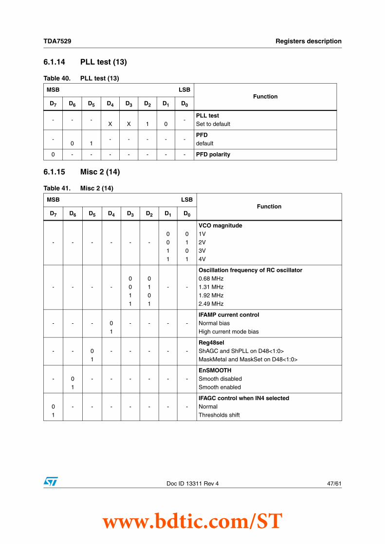
TDA7529 Registers description
Doc ID 13311 Rev 4 47/61
6.1.14 PLL test (13)
6.1.15 Misc 2 (14)
Table 40. PLL test (13)
MSB LSBFunction
D7 D6 D5 D4 D3 D2 D1 D0
- - -X X 1 0
-PLL testSet to default
-0 1
- - - - -PFD default
0 - - - - - - - PFD polarity
Table 41. Misc 2 (14)
MSB LSBFunction
D7 D6 D5 D4 D3 D2 D1 D0
- - - - - -
0
01
1
0
10
1
VCO magnitude1V
2V3V
4V
- - - -
0
01
1
0
10
1
- -
Oscillation frequency of RC oscillator0.68 MHz
1.31 MHz1.92 MHz
2.49 MHz
- - - 0
1
- - - -
IFAMP current controlNormal bias
High current mode bias
- - 01
- - - - -
Reg48selShAGC and ShPLL on D48<1:0>MaskMetal and MaskSet on D48<1:0>
- 0
1
- - - - - -EnSMOOTHSmooth disabled
Smooth enabled
0
1
- - - - - - -
IFAGC control when IN4 selectedNormal
Thresholds shift
www.bdtic.com/ST

Registers description TDA7529
48/61 Doc ID 13311 Rev 4
6.1.16 Wait lock (15)
6.1.17 AGC time constant settings (16 / 32)
Table 42. Wait lock (15)
MSB LSBFunction
D7 D6 D5 D4 D3 D2 D1 D0
- - - - - -
0
0
11
0
1
01
TestD18<0>
LOCK_bit
CMPoutVdivOUT
0
0
1
0
0
1
0
1
1
0
1
1
0
0
1
- - -
Wait lock0.04ms (min. value)
1ms (default value)
5.08ms (default value)
Table 43. AGC time constant settings (16 / 32)
MSB LSBFunction
D7 D6 D5 D4 D3 D2 D1 D0
- - - - - -0
01
0
10
FM AGC decay time constantD1
D2D3
- - - -0
0
1
0
1
0
- -
FM AGC attack time constantA1
A2
A3
- -00
1
01
0
- - - -
AM AGC time constantT1T2
T3
- 0
1
- - - - - -
IF AGC time constant FMU1
U2
01
- - - - - - -
IF AGC time constant AMS1S2
www.bdtic.com/ST

TDA7529 Registers description
Doc ID 13311 Rev 4 49/61
6.1.18 AMAGC control (17 / 33)
Table 44. AMAGC control (17 / 33
MSB LSBFunction
D7 D6 D5 D4 D3 D2 D1 D0
- - - - - -
0
0
11
0
1
01
AM AGC voltage output modeOff
Voltage output / sense internal
CalibrationVoltage output / sense external
- - - -
0
0
11
0
1
01
- -
AM AGC current output modeOff
Constant 2mA
Positive currentN/A
00
0
00
0
00
1
11
1
11
1
1
00
0
01
1
11
0
00
0
11
1
1
00
1
10
0
11
0
01
1
00
1
1
01
0
10
1
01
0
10
1
01
0
1
- - - -
AM AGC thresholdsMixer input level = 94 dBµVMixer input level = 95 dBµV
Mixer input level = 96 dBµV
Mixer input level = 97 dBµVMixer input level = 98 dBµV
Mixer input level = 99 dBµV
Mixer input level = 100 dBµVMixer input level = 101 dBµV
Mixer input level = 94 dBµV
Mixer input level = 93 dBµVMixer input level = 92 dBµV
Mixer input level = 91 dBµV
Mixer input level = 90 dBµVMixer input level = 89 dBµV
Mixer input level = 88 dBµV
Mixer input level = 87 dBµV
www.bdtic.com/ST

Registers description TDA7529
50/61 Doc ID 13311 Rev 4
6.1.19 GPIO output level control (18 / 34)
6.1.20 IF control (19 / 35)
Table 45. GPIO output level control (18 / 34)
MSB LSBFunction
D7 D6 D5 D4 D3 D2 D1 D0
0
1
:X:
:X:
:
X:
:
X:
:
X:
01
0
1
GPIOx high / low output levelGPIO1 low
GPIO1 highGPIO2 low
GPIO2 high
:GPIOx low / high:GPIO8 low
GPIO8 high
Table 46. IF control (19 / 35)
MSB LSBFunction
D7 D6 D5 D4 D3 D2 D1 D0
- - - - - - - X Not used
- - - - - - 0
1
-RC testTest enabled
Test disabled
- - - - - 0
1
- -
AMAGC input bufferBuffer enabled
Buffer disabled
- - - - 01
- - -Mixer input selection for FMFM1 mixer input
FM2 mixer input
-
0
0
:1
1
0
0
:1
1
0
1
:0
1
- - - -
IF amplifier Gain25dB (input1-3) / 19dB (input4)
27dB (input1-3) / 21dB (input4)
:37dB (input1-3) / 31dB (input4)
39dB (input1-3) / 33dB (input4)
0
1
- - - - - - -
IF input selection analog / IBOCIBOC
Analog
www.bdtic.com/ST

TDA7529 Registers description
Doc ID 13311 Rev 4 51/61
6.1.21 AF state machine wait time 1 (20 / 36)
6.1.22 PLL main divider (N-divider) 1 (21 / 37)
6.1.23 PLL main divider (N-divider) 2 (22 / 38)
Table 47. AF state machine wait time 1 (20 / 36)
MSB LSBFunction
D7 D6 D5 D4 D3 D2 D1 D0
- - - - - - - X Not used
- - - - - - X Not used
0
0
0
0
0
1
0
1
0
0
0
0
- -
WAIT 1ms0.04ms (min. value)
1ms (default value)
Table 48. PLL main divider (N-divider) 1 (21 / 37)
MSB LSBFunction
D7 D6 D5 D4 D3 D2 D1 D0
X
X
XX
X
XX
X
Divider N valueM8
M9M10
M11
M12M13
M14
M15
Table 49. PLL main divider (N-divider) 2 (22 / 38)
MSB LSBFunction
D7 D6 D5 D4 D3 D2 D1 D0
XX
X
XX
X
XX
Divider N valueM0M1
M2
M3M4
M5
M6M7
www.bdtic.com/ST

Registers description TDA7529
52/61 Doc ID 13311 Rev 4
6.1.24 PLL main divider (N-divider) 3 (23 / 39)
6.1.25 PLL Divider ratio calculation
6.1.26 VCO divider (V-divider) (24 / 40)
Table 50. PLL main divider (N-divider) 3 (23 / 39)
MSB LSBFunction
D7 D6 D5 D4 D3 D2 D1 D0
X
XX
X
X
- - -
Divider N valueA0
A1
A2A3
A4
Table 51. PLL Divider ratio calculation
M counter A counter Notes
M16 M15 … M7 … M1 M0 A4 A3 A2 A1 A0N= 32*P + A M=32N= M*P + A M>32
(P=32)
Table 52. VCO divider (V-divider) (24 / 40)
MSB LSBFunction
D7 D6 D5 D4 D3 D2 D1 D0
-
X
XX
X
XX
X
Divider V valueV0
V1V2
V3
V4V5
V6
0
1
- - - - - - -
VCO range selectionRange 2
Range 1
www.bdtic.com/ST
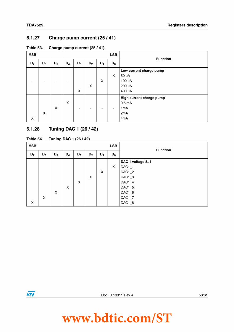
TDA7529 Registers description
Doc ID 13311 Rev 4 53/61
6.1.27 Charge pump current (25 / 41)
6.1.28 Tuning DAC 1 (26 / 42)
Table 53. Charge pump current (25 / 41)
MSB LSBFunction
D7 D6 D5 D4 D3 D2 D1 D0
- - - -
XX
X
XLow current charge pump 50 µA
100 µA
200 µA400 µA
XX
X
X
- - - -
High current charge pump0.5 mA
1mA
2mA4mA
Table 54. Tuning DAC 1 (26 / 42)
MSB LSBFunction
D7 D6 D5 D4 D3 D2 D1 D0
XX
X
XX
X
XX
DAC 1 voltage 8..1DAC1_.DAC1_2
DAC1_3
DAC1_4DAC1_5
DAC1_6
DAC1_7DAC1_8
www.bdtic.com/ST

Registers description TDA7529
54/61 Doc ID 13311 Rev 4
6.1.29 Tuning DAC 2 (27 / 43)
Note: DAC output voltage = 600mV + DACval * 9mV
6.1.30 Different controls (28 / 44)
Table 55. Tuning DAC 2 (27 / 43)
MSB LSBFunction
D7 D6 D5 D4 D3 D2 D1 D0
X
XX
X
XX
X
XDAC 2 voltage 8..1DAC2_1
DAC2_2
DAC2_3DAC2_4
DAC2_5
DAC2_6DAC2_7
DAC2_8
Table 56. Different controls (28 / 44)
MSB LSBFunction
D7 D6 D5 D4 D3 D2 D1 D0
- - - - - - - 0
1
DAC 1 On / OffOff
On
- - - - - - 01
-
DAC 2 On / OffOffOn
- - - - - X - - DAC 1_0
- - - - X - - - DAC 2_0
- - X X - - - - Not used
- X - - - - - - Not used
01
- - - - - - -
IQ phase selectI anticipates QQ anticipates I
www.bdtic.com/ST

TDA7529 Registers description
Doc ID 13311 Rev 4 55/61
6.1.31 Misc 3 (29 / 45)
6.1.32 Analog test select (30 / 46)
Table 57. Misc 3 (29 / 45)
MSB LSBFunction
D7 D6 D5 D4 D3 D2 D1 D0
- - - - - - -X
PLL N divider MSBM16
- - - - - - X Not used
00
1
01
1
01
1
00
1
00
1
01
1
- -
WAIT 2ms0.08ms (min. value)2ms (default value)
5.04ms (default value)
Table 58. Analog test select (30 / 46)
MSB LSBFunction
D7 D6 D5 D4 D3 D2 D1 D0
- - - - - -
0
0
11
0
1
01
Analog test output signal selectIF AGC
FM AGC
AMAGCDAC voltage of ADC
0
0
1
0
0
1
0
0
1
0
1
1
0
1
1
0
0
1
- -
WAIT 0.5ms0.02ms (min. value)
0.5ms (default value)
5.06ms (max value)
www.bdtic.com/ST

Registers description TDA7529
56/61 Doc ID 13311 Rev 4
6.1.33 AD converter test (31 / 47)
6.1.34 Read 1 (48)
Table 59. AD converter test (31 / 47)
MSB LSBFunction
D7 D6 D5 D4 D3 D2 D1 D0
- -
X
X
XX
X
XADC DAC direct programmingDAC 0
DAC 1
DAC 2DAC 3
DAC 4
DAC 5
- 01
- - - - - -
ADC test enableOffOn
01
- - - - - - -
AGC test enableOffOn
Table 60. Read 1 (48)
MSB LSBFunction
D7 D6 D5 D4 D3 D2 D1 D0
- - - - - -
0
0
11
0
1
01
Mask set revisionA
B
CD
- - - -
0
0
11
0
1
01
- -
Metal mask revisionA
B
CD
- - - 0
1
- - - -GPIO 5 levellowhigh
- - 0
1
- - - - -
GPIO 6 levellow
high
www.bdtic.com/ST
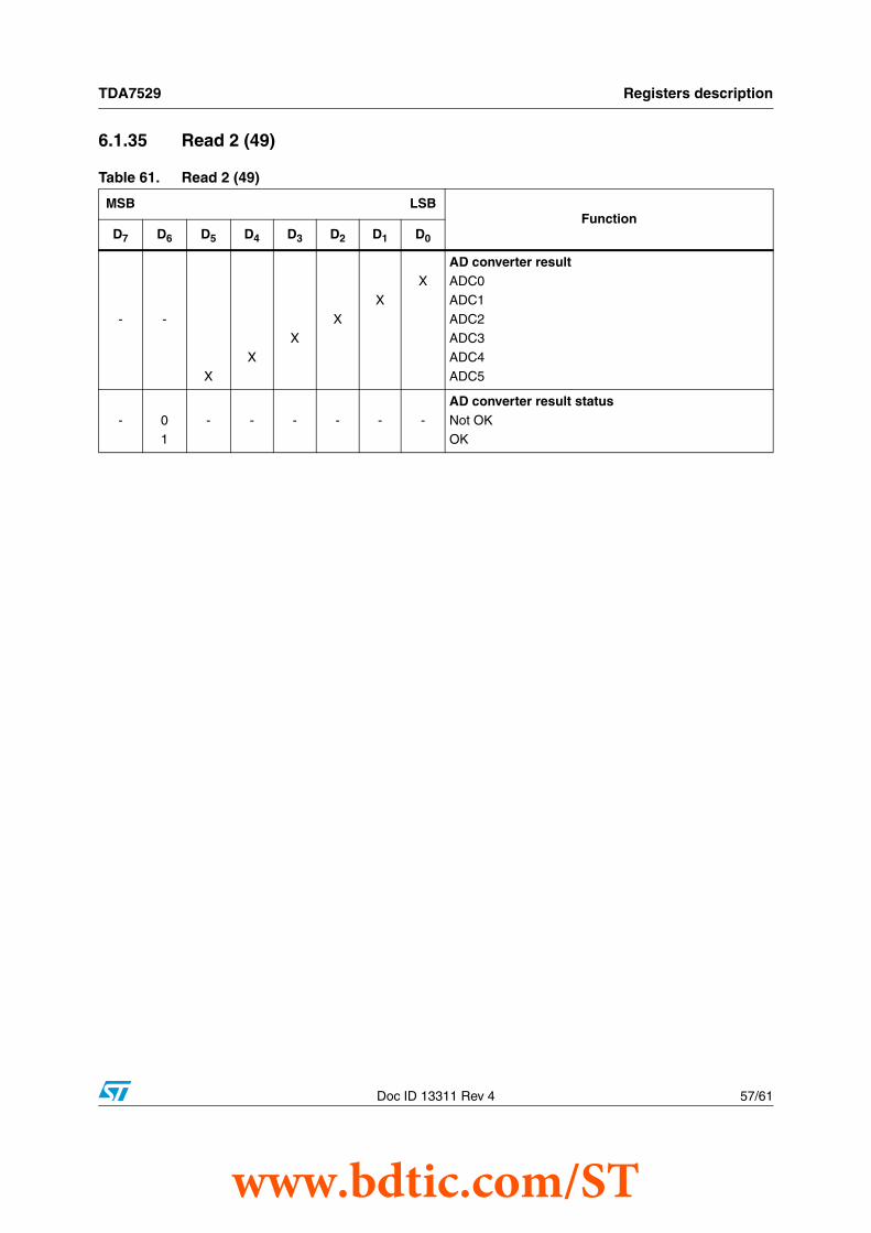
TDA7529 Registers description
Doc ID 13311 Rev 4 57/61
6.1.35 Read 2 (49)
Table 61. Read 2 (49)
MSB LSBFunction
D7 D6 D5 D4 D3 D2 D1 D0
- -
X
X
XX
X
XAD converter resultADC0
ADC1
ADC2ADC3
ADC4
ADC5
- 01
- - - - - -
AD converter result statusNot OKOK
www.bdtic.com/ST

Application schematic TDA7529
58/61 Doc ID 13311 Rev 4
7 Application schematic
Figure 16. Application schematic
www.bdtic.com/ST

TDA7529 Package information
Doc ID 13311 Rev 4 59/61
8 Package information
In order to meet environmental requirements, ST offers these devices in different grades of ECOPACK® packages, depending on their level of environmental compliance. ECOPACK®
specifications, grade definitions and product status are available at: www.st.com.
ECOPACK® is an ST trademark.
Figure 17. LQFP64 (10x10x1.4mm) exposed pad down mechanical data and package dimensions (exposed pad size for D2 and E2: 4.5mm max.)
www.bdtic.com/ST

Revision history TDA7529
60/61 Doc ID 13311 Rev 4
9 Revision history
Table 62. Document revision history
Date Revision Changes
07-Mar-2007 1 Initial release.
04-Jun-2007 2 Minor text changes.
17-Dec-2009 3 Modify Table 24: Serial data interface on page 28.
12_apr-2011 4Removed the obsolete order code “TDA7529” and added the order code “TDA7529TX” in Table 1: Device summary on page 1.Reformatted “Registers description” information.
www.bdtic.com/ST

TDA7529
Doc ID 13311 Rev 4 61/61
Please Read Carefully:
Information in this document is provided solely in connection with ST products. STMicroelectronics NV and its subsidiaries (“ST”) reserve theright to make changes, corrections, modifications or improvements, to this document, and the products and services described herein at anytime, without notice.
All ST products are sold pursuant to ST’s terms and conditions of sale.
Purchasers are solely responsible for the choice, selection and use of the ST products and services described herein, and ST assumes noliability whatsoever relating to the choice, selection or use of the ST products and services described herein.
No license, express or implied, by estoppel or otherwise, to any intellectual property rights is granted under this document. If any part of thisdocument refers to any third party products or services it shall not be deemed a license grant by ST for the use of such third party productsor services, or any intellectual property contained therein or considered as a warranty covering the use in any manner whatsoever of suchthird party products or services or any intellectual property contained therein.
UNLESS OTHERWISE SET FORTH IN ST’S TERMS AND CONDITIONS OF SALE ST DISCLAIMS ANY EXPRESS OR IMPLIEDWARRANTY WITH RESPECT TO THE USE AND/OR SALE OF ST PRODUCTS INCLUDING WITHOUT LIMITATION IMPLIEDWARRANTIES OF MERCHANTABILITY, FITNESS FOR A PARTICULAR PURPOSE (AND THEIR EQUIVALENTS UNDER THE LAWSOF ANY JURISDICTION), OR INFRINGEMENT OF ANY PATENT, COPYRIGHT OR OTHER INTELLECTUAL PROPERTY RIGHT.
UNLESS EXPRESSLY APPROVED IN WRITING BY AN AUTHORIZED ST REPRESENTATIVE, ST PRODUCTS ARE NOTRECOMMENDED, AUTHORIZED OR WARRANTED FOR USE IN MILITARY, AIR CRAFT, SPACE, LIFE SAVING, OR LIFE SUSTAININGAPPLICATIONS, NOR IN PRODUCTS OR SYSTEMS WHERE FAILURE OR MALFUNCTION MAY RESULT IN PERSONAL INJURY,DEATH, OR SEVERE PROPERTY OR ENVIRONMENTAL DAMAGE. ST PRODUCTS WHICH ARE NOT SPECIFIED AS "AUTOMOTIVEGRADE" MAY ONLY BE USED IN AUTOMOTIVE APPLICATIONS AT USER’S OWN RISK.
Resale of ST products with provisions different from the statements and/or technical features set forth in this document shall immediately voidany warranty granted by ST for the ST product or service described herein and shall not create or extend in any manner whatsoever, anyliability of ST.
ST and the ST logo are trademarks or registered trademarks of ST in various countries.
Information in this document supersedes and replaces all information previously supplied.
The ST logo is a registered trademark of STMicroelectronics. All other names are the property of their respective owners.
© 2011 STMicroelectronics - All rights reserved
STMicroelectronics group of companies
Australia - Belgium - Brazil - Canada - China - Czech Republic - Finland - France - Germany - Hong Kong - India - Israel - Italy - Japan - Malaysia - Malta - Morocco - Philippines - Singapore - Spain - Sweden - Switzerland - United Kingdom - United States of America
www.st.com
www.bdtic.com/ST