
Revisiting the theory of ferroelectric negative capacitance · 2016-05-24 · 1 Revisiting the...
7
1 Revisiting the theory of ferroelectric negative capacitance Kausik Majumdar 1† , Suman Datta 2 , and Satyavolu Papa Rao 3 Abstract—In this paper we revisit the theory of negative capacitance, in a (i) standalone ferroelectric, (ii) ferroelectric- dielectric, and (iii) ferroelectric-semiconductor series combina- tion, and show that it is important to minimize the total Gibbs free energy of the combined system (and not just the free energy of the ferroelectric) to obtain the correct states. The theory is explained both analytically and using numerical simulation, for ferroelectric materials with first order and second order phase transitions. The exact conditions for different regimes of opera- tion in terms of hysteresis and gain are derived for ferroelectric- dielectric combination. Finally the ferroelectric-semiconductor series combination is analyzed to gain insights into the possibility of realization of steep slope transistors in a hysteresis free manner. I. I NTRODUCTION Reducing the supply voltage while maintaining the perfor- mance is one of the key focus areas of current device research, which would enable reduction of power consumption up to the system level [1]. It is well known that the long high energy tail of the Fermi-Dirac distribution of carrier population at the source junction does not allow the MOSFET current to be changed by any more than a decade for every 60 mV change in the gate voltage at room temperature. This is a fundamental bottleneck of MOSFET operation that limits the supply voltage scaling. Ways to beat this subthreshold slope limit of 60 mV/decade have been intensely investigated in the past [2]-[6]. To this end, ferroelectric negative capacitance FET (Ferro- FET) was proposed [6] where the gate insulator of a MOSFET is replaced by a ferroelectric material. With an increase in the gate voltage (over a certain range), the internal “negative capacitance” of the ferroelectric forces the voltage drop across itself to decrease, which in turn increases the channel surface potential of the semiconductor by a value which is more than the change of the gate voltage. Such a gain mechanism between the external gate voltage and the internal channel surface potential allows for a larger change in drain current than what is predicted by 60 mV/decade, even though the current-surface potential relationship is still limited by the tail of the Fermi-Dirac distribution [6]-[16]. One question that is frequently asked in this context is whether it is possible to maintain such voltage gain in a hysteresis free way so as to achieve the eventual goal of reducing supply voltage of digital logic. In the recent past, 1 Department of Electrical Communication Engineering, Indian Institute of Science, Bangalore 560012, India. 2 Department of Electrical Engineering, University of Notre Dame, Notre Dame, IN 46556-5637 USA. 3 SUNY Poly SEMATECH, 257 Fuller Road, Albany, NY 12203, USA, † Corresponding author, Email: [email protected] there have been a number of efforts to investigate this, both theoretically [6]-[11] and experimentally [12]-[13]. However, a clear understanding of the mechanism of such devices is still lacking in the literature, which is partly due to the solution methodology typically adopted - by minimizing the Gibbs free energy for the ferroelectric and then equating the ferroelectric polarization at the minimum energy point to the charge per unit area of the series capacitance [6]-[11]. Unfortunately, this does not necessarily minimize the total Gibbs free energy of the combined system since both components (ferroelectric and series capacitance) can have complex dependence of free energy on appropriate state variable. It turns out that although both the approaches gives rise to same results for a linear capacitor placed in series with the ferroelectric, the results can be quite different when the series capacitance is non-linear in nature (for example, semiconductor channel). Our aim in this paper is threefold: (i) to establish a theory based on the minimization of Gibbs free energy of the whole system, (ii) to find the exact conditions for hysteresis free gain in a ferroelectric-dielectric series combination to check if it is possible to have a design window for such operation, and (iii) to understand a FerroFET operation using a one dimensional FerroMOSCAP analysis to elucidate whether a sub-60 mV/decade operation is possible in a hysteresis free manner. The rest of the paper is organized as follows: The method of Gibbs free energy minimization is established using a simple example of two linear dielectric capacitors in series in sec. II. The concept of negative capacitance is then explained using a single standalone ferroelectric capacitor in sec. III. This is followed by a detailed analysis of ferroelectric-dielectric series combination in sec. IV. The FerroMOSCAP analysis is performed in sec. V, which is followed by discussion on some practical aspects in sec. VI. Conclusions that can be drawn are presented in sec. VII. II. METHOD OF GIBBS FREE ENERGY MINIMIZATION When a system is excited by an external stimulus X, and if Y is an appropriate internal state variable, the system reorganizes Y in such a manner that the Gibbs free energy of the whole system is minimized. To explain this, we use a simple example of two capacitors, with C 1 and C 2 being the capacitance per unit area, connected in series and excited by an external voltage V , as shown in the inset of Fig. 1. For isothermal process and in the absence of any stress, the Gibbs free energy (ΔG) of a dielectric capacitor is just the electrostatic energy R ¯ D · d ¯ E, where ¯ D is the displacement arXiv:1605.06621v1 [cond-mat.mes-hall] 21 May 2016
Transcript of Revisiting the theory of ferroelectric negative capacitance · 2016-05-24 · 1 Revisiting the...
1
Revisiting the theory of ferroelectric negativecapacitance
Kausik Majumdar1†, Suman Datta2, and Satyavolu Papa Rao3
Abstract—In this paper we revisit the theory of negativecapacitance, in a (i) standalone ferroelectric, (ii) ferroelectric-dielectric, and (iii) ferroelectric-semiconductor series combina-tion, and show that it is important to minimize the total Gibbsfree energy of the combined system (and not just the free energyof the ferroelectric) to obtain the correct states. The theory isexplained both analytically and using numerical simulation, forferroelectric materials with first order and second order phasetransitions. The exact conditions for different regimes of opera-tion in terms of hysteresis and gain are derived for ferroelectric-dielectric combination. Finally the ferroelectric-semiconductorseries combination is analyzed to gain insights into the possibilityof realization of steep slope transistors in a hysteresis free manner.
I. INTRODUCTION
Reducing the supply voltage while maintaining the perfor-mance is one of the key focus areas of current device research,which would enable reduction of power consumption up to thesystem level [1]. It is well known that the long high energytail of the Fermi-Dirac distribution of carrier population atthe source junction does not allow the MOSFET current tobe changed by any more than a decade for every 60 mVchange in the gate voltage at room temperature. This is afundamental bottleneck of MOSFET operation that limits thesupply voltage scaling. Ways to beat this subthreshold slopelimit of 60 mV/decade have been intensely investigated in thepast [2]-[6].
To this end, ferroelectric negative capacitance FET (Ferro-FET) was proposed [6] where the gate insulator of a MOSFETis replaced by a ferroelectric material. With an increase inthe gate voltage (over a certain range), the internal “negativecapacitance” of the ferroelectric forces the voltage drop acrossitself to decrease, which in turn increases the channel surfacepotential of the semiconductor by a value which is morethan the change of the gate voltage. Such a gain mechanismbetween the external gate voltage and the internal channelsurface potential allows for a larger change in drain currentthan what is predicted by 60 mV/decade, even though thecurrent-surface potential relationship is still limited by the tailof the Fermi-Dirac distribution [6]-[16].
One question that is frequently asked in this context iswhether it is possible to maintain such voltage gain in ahysteresis free way so as to achieve the eventual goal ofreducing supply voltage of digital logic. In the recent past,
1Department of Electrical Communication Engineering, Indian Institute ofScience, Bangalore 560012, India. 2Department of Electrical Engineering,University of Notre Dame, Notre Dame, IN 46556-5637 USA. 3SUNY PolySEMATECH, 257 Fuller Road, Albany, NY 12203, USA, †Correspondingauthor, Email: [email protected]
there have been a number of efforts to investigate this, boththeoretically [6]-[11] and experimentally [12]-[13]. However,a clear understanding of the mechanism of such devices isstill lacking in the literature, which is partly due to the solutionmethodology typically adopted - by minimizing the Gibbs freeenergy for the ferroelectric and then equating the ferroelectricpolarization at the minimum energy point to the charge perunit area of the series capacitance [6]-[11]. Unfortunately, thisdoes not necessarily minimize the total Gibbs free energyof the combined system since both components (ferroelectricand series capacitance) can have complex dependence offree energy on appropriate state variable. It turns out thatalthough both the approaches gives rise to same results fora linear capacitor placed in series with the ferroelectric, theresults can be quite different when the series capacitance isnon-linear in nature (for example, semiconductor channel).Our aim in this paper is threefold: (i) to establish a theorybased on the minimization of Gibbs free energy of the wholesystem, (ii) to find the exact conditions for hysteresis freegain in a ferroelectric-dielectric series combination to check ifit is possible to have a design window for such operation,and (iii) to understand a FerroFET operation using a onedimensional FerroMOSCAP analysis to elucidate whether asub-60 mV/decade operation is possible in a hysteresis freemanner.
The rest of the paper is organized as follows: The method ofGibbs free energy minimization is established using a simpleexample of two linear dielectric capacitors in series in sec. II.The concept of negative capacitance is then explained usinga single standalone ferroelectric capacitor in sec. III. Thisis followed by a detailed analysis of ferroelectric-dielectricseries combination in sec. IV. The FerroMOSCAP analysis isperformed in sec. V, which is followed by discussion on somepractical aspects in sec. VI. Conclusions that can be drawn arepresented in sec. VII.
II. METHOD OF GIBBS FREE ENERGY MINIMIZATION
When a system is excited by an external stimulus X , andif Y is an appropriate internal state variable, the systemreorganizes Y in such a manner that the Gibbs free energyof the whole system is minimized. To explain this, we usea simple example of two capacitors, with C1 and C2 beingthe capacitance per unit area, connected in series and excitedby an external voltage V , as shown in the inset of Fig. 1.For isothermal process and in the absence of any stress, theGibbs free energy (∆G) of a dielectric capacitor is just theelectrostatic energy
∫D · dE, where D is the displacement
arX
iv:1
605.
0662
1v1
[co
nd-m
at.m
es-h
all]
21
May
201
6
2
V
Vi
𝐶1
𝐶2
DG
(J/
m2)
Q (C/m2)
DG2
DG1
DGB
DG= DG1+ DG2+ DGB
DGmin
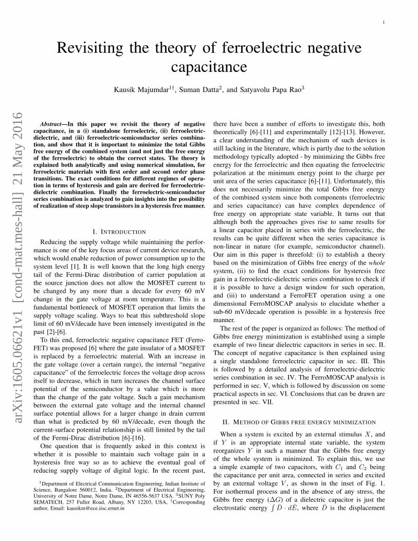
Fig. 1. Gibbs free energy (∆G) of two capacitors (1 and 4 F/m2 in series,with an applied bias V = 5 V. The individual Gibbs free energy of the twocapacitors (∆G1,2) and the battery (∆GB) are also shown. The minima of∆G1,2 do not coincide with total free energy minimum.
vector and E is the electric field. In this paper, we assume allquantities to be uniform in-plane and perform one dimensionalanalysis, removing the vector signs for simplicity. D thenbecomes equal to the charge per unit area (Q) at the capacitorplates. The ∆G of the combined system is given by
∆G =Q2
2C1+
Q2
2C2−QV (1)
where V is the external supply voltage. For a given V , thesystem will settle Q in such a way that ∆G is minimized,i.e. ∂∆G
∂Q = 0 and ∂2∆G∂Q2 > 0, which gives rise to the well
known result of combined capacitance C = QV = C1
C1+C2. The
same result is readily obtained electrostatically by equating thecharges on the capacitor plates, i.e. C1(V −Vi) = C2Vi whereVi is the internal node voltage. It’s interesting to note from Fig.1 that when ∆G is minimized, both ∆G1 and ∆G2 are abovetheir individual minimum due to non-monotonic dependenceof ∆G1,2 on Q. This leads to an important conclusion thatwhen a system stabilizes in its Gibbs free energy minimum, thesubsystems may not necessarily be in their individual energyminimum with respect to the internal state variable.
III. A STANDALONE FERROELECTRIC CAPACITOR
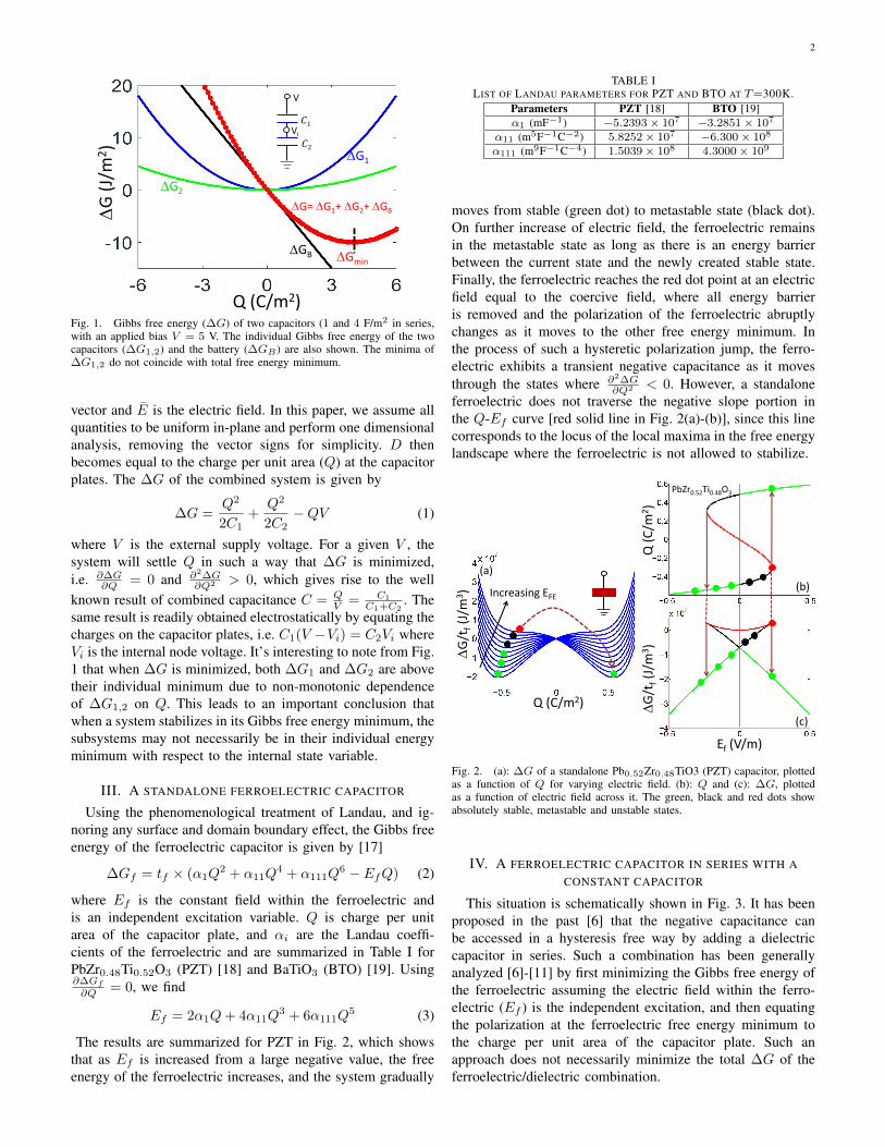
Using the phenomenological treatment of Landau, and ig-noring any surface and domain boundary effect, the Gibbs freeenergy of the ferroelectric capacitor is given by [17]
∆Gf = tf × (α1Q2 + α11Q
4 + α111Q6 − EfQ) (2)
where Ef is the constant field within the ferroelectric andis an independent excitation variable. Q is charge per unitarea of the capacitor plate, and αi are the Landau coeffi-cients of the ferroelectric and are summarized in Table I forPbZr0.48Ti0.52O3 (PZT) [18] and BaTiO3 (BTO) [19]. Using∂∆Gf
∂Q = 0, we find
Ef = 2α1Q+ 4α11Q3 + 6α111Q
5 (3)
The results are summarized for PZT in Fig. 2, which showsthat as Ef is increased from a large negative value, the freeenergy of the ferroelectric increases, and the system gradually
TABLE ILIST OF LANDAU PARAMETERS FOR PZT AND BTO AT T=300K.
Parameters PZT [18] BTO [19]α1 (mF−1) −5.2393× 10⁷ −3.2851× 10⁷
α11 (m5F−1C−2) 5.8252× 10⁷ −6.300× 10⁸
α111 (m9F−1C−4) 1.5039× 10⁸ 4.3000× 10⁹
moves from stable (green dot) to metastable state (black dot).On further increase of electric field, the ferroelectric remainsin the metastable state as long as there is an energy barrierbetween the current state and the newly created stable state.Finally, the ferroelectric reaches the red dot point at an electricfield equal to the coercive field, where all energy barrieris removed and the polarization of the ferroelectric abruptlychanges as it moves to the other free energy minimum. Inthe process of such a hysteretic polarization jump, the ferro-electric exhibits a transient negative capacitance as it movesthrough the states where ∂2∆G
∂Q2 < 0. However, a standaloneferroelectric does not traverse the negative slope portion inthe Q-Ef curve [red solid line in Fig. 2(a)-(b)], since this linecorresponds to the locus of the local maxima in the free energylandscape where the ferroelectric is not allowed to stabilize.
DG
/tf(J
/m3)
Q (
C/m
2)
Ef (V/m)
PbZr0.52Ti0.48O3
(b)
(c)
DG
/tf(J
/m3)
Q (C/m2)
Increasing EFE
(a)
Fig. 2. (a): ∆G of a standalone Pb0.52Zr0.48TiO3 (PZT) capacitor, plottedas a function of Q for varying electric field. (b): Q and (c): ∆G, plottedas a function of electric field across it. The green, black and red dots showabsolutely stable, metastable and unstable states.
IV. A FERROELECTRIC CAPACITOR IN SERIES WITH ACONSTANT CAPACITOR
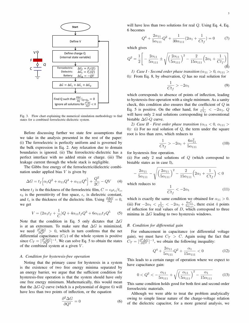
This situation is schematically shown in Fig. 3. It has beenproposed in the past [6] that the negative capacitance canbe accessed in a hysteresis free way by adding a dielectriccapacitor in series. Such a combination has been generallyanalyzed [6]-[11] by first minimizing the Gibbs free energy ofthe ferroelectric assuming the electric field within the ferro-electric (Ef ) is the independent excitation, and then equatingthe polarization at the ferroelectric free energy minimum tothe charge per unit area of the capacitor plate. Such anapproach does not necessarily minimize the total ∆G of theferroelectric/dielectric combination.
3
Start
Define V
V
F
C
Define charge Q (internal state variable)
Δ𝐺𝑓 = 𝐹𝑓(𝑄)Δ𝐺𝑐 = 𝐹𝑐(𝑄)Δ𝐺𝐵 = −𝑄𝑉
Ferroelectric:
Dielectric:
Battery:
Δ𝐺 = Δ𝐺𝑓 + Δ𝐺𝑐 + Δ𝐺𝐵
Find Q such that 𝜕Δ𝐺
𝜕𝑄|𝑄=𝑄0 = 0
Ignore all solutions for𝜕2Δ𝐺
𝜕𝑄2< 0
Q
Fig. 3. Flow chart explaining the numerical simulation methodology to findstates for a combined ferroelectric-dielectric system.
Before discussing further we state few assumptions thatwe take in the analysis presented in the rest of the paper:(i) The ferroelectric is perfectly uniform and is governed bythe bulk expression in Eq. 2. Any relaxation due to domainboundaries is ignored. (ii) The ferroelectric-dielectric has aperfect interface with no added strain or charge. (iii) Theleakage current through the whole stack is negligible.
The Gibbs free energy of the ferroelectric/dielectric combi-nation under applied bias V is given by
∆G = tf
[α1Q
2 + α11Q4 + α111Q
6]
+Q2
2C−QV (4)
where tf is the thickness of the ferroelectric film, C = ε0εc/tc,ε0 is the permittivity of free space, εc is dielectric constant,and tc is the thickness of the dielectric film. Using ∂∆G
∂Q = 0,we get
V = (2α1tf +1
C)Q+ 4α11tfQ
3 + 6α111tfQ5 (5)
Note that the condition in Eq. 5 only dictates that ∆Gis at an extremum. To make sure that ∆G is minimized,we need ∂2∆G
∂Q2 > 0, which in turn confirms that the netdifferential capacitance (CT ) of the whole system is positivesince CT = [∂
2∆G∂Q2 ]−1. We can solve Eq. 5 to obtain the states
of the combined system at a given V .
A. Condition for hysteresis-free operation
Noting that the primary cause for hysteresis in a systemis the existence of two free energy minima separated byan energy barrier, we argue that the sufficient condition forhysteresis-free operation is that the system should have onlyone free energy minimum. Mathematically, this would meanthat the ∆G-Q curve (which is a polynomial of degree 6) willhave less than two points of inflection, or the equation
∂2∆G
∂Q2= 0 (6)
will have less than two solutions for real Q. Using Eq. 4, Eq.6 becomes
Q4 +2α11
5α111Q2 +
1
30α111(2α1 +
1
Ctf) = 0 (7)
which gives
Q2 =1
2
[− 2α11
5α111±
√( 2α11
5α111
)2
− 2
15α111
(2α1 +
1
Ctf
)](8)
1) Case I - Second order phase transition (α11 > 0, α111 >0): From Eq. 8, by observation, Q has no real solution for
1
Ctf> −2α1 (9)
which corresponds to absence of points of inflection, leadingto hysteresis-free operation with a single minimum. As a sanitycheck, this condition also ensures that the coefficient of Q inEq. 5 is positive. On the other hand, for 1
Ctf< −2α1, Q
will have only 2 real solutions corresponding to conventionalbistable ∆G-Q curve.
2) Case II - First order phase transition (α11 < 0, α111 >0): (i) For no real solution of Q, the term under the squareroot is less than zero, which reduces to
1
Ctf> −2α1 +
6α211
5α111(10)
for hysteresis free operation.(ii) For only 2 real solutions of Q (which correspond tobistable states as in case I),
− 2α11
5α111−
√( 2α11
5α111
)2
− 2
15α111
(2α1 +
1
Ctf
)< 0
which reduces to1
Ctf< −2α1 (11)
which is exactly the same condition we obtained for α11 > 0.(iii) For −2α1 <
1Ctf
< −2α1 +6α2
11
5α111, there exist 4 points
of inflection for real values of D, which correspond to threeminima in ∆G leading to two hysteresis windows.
B. Condition for differential gain
For enhancement in capacitance (or differential voltagegain), we must have CT > C. Again using the fact thatCT = [∂
2∆G∂D2 ]−1, we obtain the following inequality:
Q4 +2α11
5α111Q2 +
α1
15α111< 0 (12)
This leads to a certain range of operation where we expect tohave capacitance gain:
0 < Q2 < − α11
5α111+
√( α11
5α111
)2
− α1
15α111(13)
This same condition holds good for both first and second orderferroelectric materials.
Although we were able to treat the problem analyticallyowing to simple linear nature of the charge-voltage relationof the dielectric capacitor, for a more general analysis, we
4
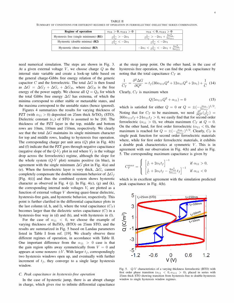
TABLE IISUMMARY OF CONDITIONS FOR DIFFERENT REGIMES OF OPERATION IN FERROELECTRIC-DIELECTRIC SERIES COMBINATION.
Regime of operation α11 > 0, α111 > 0 α11 < 0, α111 > 0
Hysteresis free (single minimum) (R1) 1Ctf
> −2α11Ctf
> −2α1 +6α2
115α111
Hysteretic (double minima) (R2) 1Ctf
< −2α11Ctf
< −2α1
Hysteretic (three minima) (R3) - −2α1 <1Ctf
< −2α1 +6α2
115α111
need numerical simulation. The steps are shown in Fig. 3.At a given external voltage V , we choose charge Q as theinternal state variable and create a look-up table based onthe general charge-Gibbs free energy relation of the genericcapacitor C and the ferroelectric. The total ∆G is then foundas ∆G = ∆Gf + ∆Gc + ∆GB , where ∆GB is the freeenergy of the power supply. We choose all Q = Q0 for whichthe total Gibbs free energy ∆G has extrema, of which theminima correspond to either stable or metastable states, andthe maxima correspond to the unstable states (hence ignored).
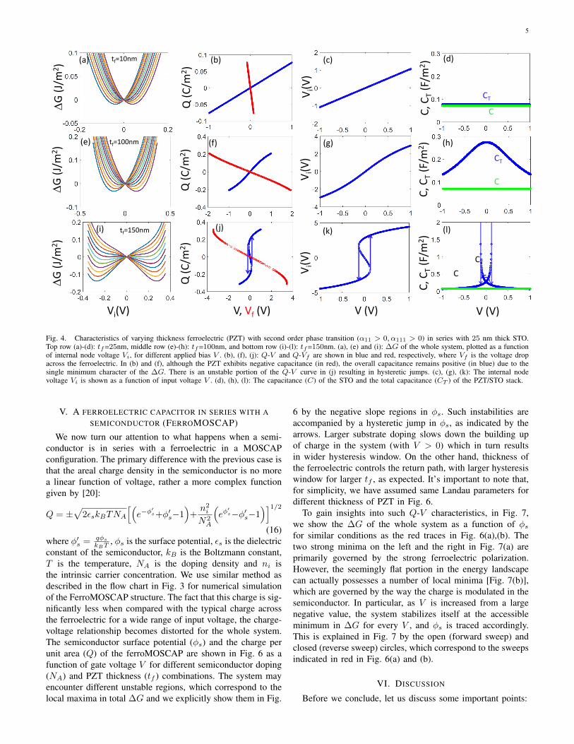
Figures 4 summarizes the results for varying thickness ofPZT (with α11 > 0) deposited on 25nm thick SrTiO3 (STO).Dielectric constant (εc) of STO is assumed to be 200. Thethickness of the PZT layer in the top, middle and bottomrows are 10nm, 100nm and 150nm, respectively. We clearlysee that the total ∆G maintains its single minimum characterfor top and middle rows, leading to hysteresis free operation.The corresponding charge per unit area (Q) plot in Fig. 4(b)and (f) indicate that the PZT goes through negative capacitance(negative slope of the Q-Vf plot in red where Vf is the voltagedrop across the ferroelectric) regime, although the slope forthe whole system (Q-V plot) remains positive (in blue), inagreement with the single minimum ∆G plot in Fig. 4(a) and(e). When the ferroelectric layer is very thick, ∆Gc cannotcompletely compensate the double minimum behavior of ∆Gf[Fig. 4(i)] and thus the combined system shows hystereticcharacter as observed in Fig. 4 (j). In Fig. 4(c), (g) and (k),the corresponding internal node voltages Vi are plotted as afunction of external voltage V showing quasi-linear dielectric,hysteresis-free gain, and hysteretic behavior, respectively. Thispoint is further clarified in the differential capacitance plots inthe last column (d, h, and l), where the total capacitance (CT )becomes larger than the dielectric series capacitance (C) in ahysteresis-free way in (d) and (h), and with hysteresis in (l).
For the case of α11 < 0, we choose the example ofvarying thickness of BaTiO3 (BTO) on 25nm STO, and theresults are summarized in Fig. 5 based on Landau parameterslisted in Table I from ref. [19]. We clearly observe threedifferent regimes of operation, in accordance with Table II.One important difference from the α11 > 0 case is thatthe gain region splits away symmetrically from V = 0 andappears at some nonzero ±V . With larger tf , correspondinglytwo hysteresis windows open up, and eventually with furtherincrement of tf , they converge to a single large hysteresiswindow.
C. Peak capacitance in hysteresis-free operationIn the case of hysteretic jump, there is an abrupt change
in charge, which gives rise to infinite differential capacitance
at the steep jump point. On the other hand, in the case ofhysteresis free operation, we can find the peak capacitance bynoting that the total capacitance CT as
1
CT=∂2∆G
∂Q2= tf (30α111Q
4 + 12α11Q2 + 2α1) +
1
C(14)
Clearly, CT is maximum when
Q(5α111Q2 + α11) = 0 (15)
which is satisfied for either Q = 0 or Q = ±(− α11
5α111)1/2.
Noting that for CT to be maximum, we need ∂2
∂Q2 ( 1CT
) =360α111tf +24α11tf > 0, we easily find that for second orderferroelectric (α11 > 0), we obtain maximum CT at Q = 0.On the other hand, for first order ferroelectric (α11 < 0), themaximum is reached for Q = ±(− α11
5α111)1/2. Clearly, CT is
single peak function for second order ferroelectric materialswhere, while for first order ferroelectric materials, it exhibitsa double peak characteristics at symmetric V . This is inagreement with our observation in Fig. 4(h) and also in Fig.5. The corresponding maximum capacitance is given by
CmaxT =
[
1C + 2α1tf
]−1
if α11 > 0,[1C + 2α1tf − 6α2
11
5α111tf
]−1
if α11 < 0
which is in excellent agreement with the simulation predictedpeak capacitance in Fig. 4(h).
V (V)
Q (
C/m
2)
tf=150nmtc=25nm (STO)
Fig. 5. Q-V characteristics of a varying thickness ferroelectric (BTO) withfirst order phase transition (α11 < 0, α111 > 0), placed in series with25nm thick STO showing transition from hysteresis-free to double-hysteresiswindow to single hysteresis window regimes.
5
Vi(V) V, Vf (V) V (V) V (V)
DG
(J/
m2)
DG
(J/
m2)
DG
(J/
m2)
Q (
C/m
2)
Q (
C/m
2)
Q(C
/m2)
Vi(V
)V
i(V)
Vi(V
)
C, C
T(F
/m2)
C, C
T(F
/m2)
C, C
T(F
/m2)
C
CT
tf=10nm
tf=100nm
tf=150nm
C
CT
(a) (b) (c) (d)
(e) (f) (g) (h)
(i) (j) (k) (l)
C
CT
Fig. 4. Characteristics of varying thickness ferroelectric (PZT) with second order phase transition (α11 > 0, α111 > 0) in series with 25 nm thick STO.Top row (a)-(d): tf=25nm, middle row (e)-(h): tf=100nm, and bottom row (i)-(l): tf=150nm. (a), (e) and (i): ∆G of the whole system, plotted as a functionof internal node voltage Vi, for different applied bias V . (b), (f), (j): Q-V and Q-Vf are shown in blue and red, respectively, where Vf is the voltage dropacross the ferroelectric. In (b) and (f), although the PZT exhibits negative capacitance (in red), the overall capacitance remains positive (in blue) due to thesingle minimum character of the ∆G. There is an unstable portion of the Q-V curve in (j) resulting in hysteretic jumps. (c), (g), (k): The internal nodevoltage Vi is shown as a function of input voltage V . (d), (h), (l): The capacitance (C) of the STO and the total capacitance (CT ) of the PZT/STO stack.
V. A FERROELECTRIC CAPACITOR IN SERIES WITH ASEMICONDUCTOR (FERROMOSCAP)
We now turn our attention to what happens when a semi-conductor is in series with a ferroelectric in a MOSCAPconfiguration. The primary difference with the previous case isthat the areal charge density in the semiconductor is no morea linear function of voltage, rather a more complex functiongiven by [20]:
Q = ±√
2εskBTNA
[(e−φ
′s+φ′s−1
)+n2i
N2A
(eφ
′s−φ′s−1
)]1/2(16)
where φ′s = qφs
kBT, φs is the surface potential, εs is the dielectric
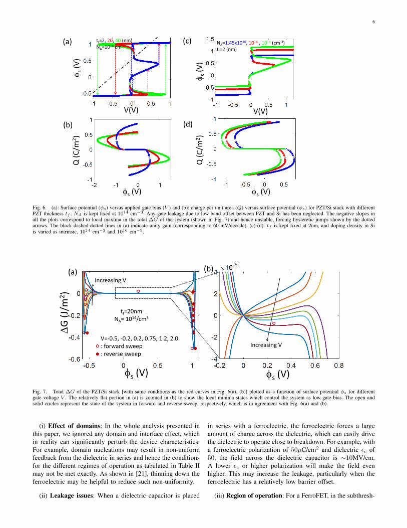
constant of the semiconductor, kB is the Boltzmann constant,T is the temperature, NA is the doping density and ni isthe intrinsic carrier concentration. We use similar method asdescribed in the flow chart in Fig. 3 for numerical simulationof the FerroMOSCAP structure. The fact that this charge is sig-nificantly less when compared with the typical charge acrossthe ferroelectric for a wide range of input voltage, the charge-voltage relationship becomes distorted for the whole system.The semiconductor surface potential (φs) and the charge perunit area (Q) of the ferroMOSCAP are shown in Fig. 6 as afunction of gate voltage V for different semiconductor doping(NA) and PZT thickness (tf ) combinations. The system mayencounter different unstable regions, which correspond to thelocal maxima in total ∆G and we explicitly show them in Fig.
6 by the negative slope regions in φs. Such instabilities areaccompanied by a hysteretic jump in φs, as indicated by thearrows. Larger substrate doping slows down the building upof charge in the system (with V > 0) which in turn resultsin wider hysteresis window. On the other hand, thickness ofthe ferroelectric controls the return path, with larger hysteresiswindow for larger tf , as expected. It’s important to note that,for simplicity, we have assumed same Landau parameters fordifferent thickness of PZT in Fig. 6.
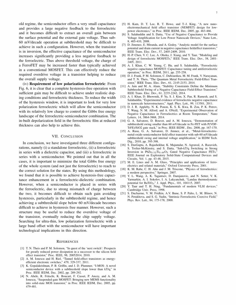
To gain insights into such Q-V characteristics, in Fig. 7,we show the ∆G of the whole system as a function of φsfor similar conditions as the red traces in Fig. 6(a),(b). Thetwo strong minima on the left and the right in Fig. 7(a) areprimarily governed by the strong ferroelectric polarization.However, the seemingly flat portion in the energy landscapecan actually possesses a number of local minima [Fig. 7(b)],which are governed by the way the charge is modulated in thesemiconductor. In particular, as V is increased from a largenegative value, the system stabilizes itself at the accessibleminimum in ∆G for every V , and φs is traced accordingly.This is explained in Fig. 7 by the open (forward sweep) andclosed (reverse sweep) circles, which correspond to the sweepsindicated in red in Fig. 6(a) and (b).
VI. DISCUSSION
Before we conclude, let us discuss some important points:
6
(a)
V(V)
(c)
fs
(V)
tf=2, 20, 40 (nm)NA=1014 cm-3
NA=1.45x10¹⁰, 1014 , 1016 (cm-3)tf=2 (nm)
V(V)
fs
(V)
fs (V)
Q (
C/m
2)
Q (
C/m
2)
fs (V)
(b) (d)
Fig. 6. (a): Surface potential (φs) versus applied gate bias (V ) and (b): charge per unit area (Q) versus surface potential (φs) for PZT/Si stack with differentPZT thickness tf . NA is kept fixed at 1014 cm−3. Any gate leakage due to low band offset between PZT and Si has been neglected. The negative slopes inall the plots correspond to local maxima in the total ∆G of the system (shown in Fig. 7) and hence unstable, forcing hysteretic jumps shown by the dottedarrows. The black dashed-dotted lines in (a) indicate unity gain (corresponding to 60 mV/decade). (c)-(d): tf is kept fixed at 2nm, and doping density in Siis varied as intrinsic, 1014 cm−3 and 1016 cm−3.
Increasing V
DG
(J/
m2)
fs (V) fs (V)
Increasing V
tf=20nmNA= 1014/cm3
V=-0.5, -0.2, 0.2, 0.75, 1.2, 2.0: forward sweep: reverse sweep
(a) (b)
Fig. 7. Total ∆G of the PZT/Si stack [with same conditions as the red curves in Fig. 6(a), (b)] plotted as a function of surface potential φs for differentgate voltage V . The relatively flat portion in (a) is zoomed in (b) to show the local minima states which control the system as low gate bias. The open andsolid circles represent the state of the system in forward and reverse sweep, respectively, which is in agreement with Fig. 6(a) and (b).
(i) Effect of domains: In the whole analysis presented inthis paper, we ignored any domain and interface effect, whichin reality can significantly perturb the device characteristics.For example, domain nucleations may result in non-uniformfeedback from the dielectric in series and hence the conditionsfor the different regimes of operation as tabulated in Table IImay not be met exactly. As shown in [21], thinning down theferroelectric may be helpful to reduce such non-uniformity.
(ii) Leakage issues: When a dielectric capacitor is placed
in series with a ferroelectric, the ferroelectric forces a largeamount of charge across the dielectric, which can easily drivethe dielectric to operate close to breakdown. For example, witha ferroelectric polarization of 50µC/cm2 and dielectric εc of50, the field across the dielectric capacitor is ∼10MV/cm.A lower εc or higher polarization will make the field evenhigher. This may increase the leakage, particularly when theferroelectric has a relatively low barrier offset.
(iii) Region of operation: For a FerroFET, in the subthresh-
7
old regime, the semiconductor offers a very small capacitanceand provides a large negative feedback to the ferroelectricand it becomes difficult to extract an overall gain betweenthe surface potential and the external gate voltage. Thus sub-60 mV/decade operation at subthreshold may be difficult toachieve in such a configuration. However, when the transistoris in inversion, the effective capacitance of the semiconductorincreases significantly providing a less negative feedback tothe ferroelectric. Thus above threshold voltage, the charge ofa FerroFET may be increased faster than typically achievedin a conventional MOSFET. This can effectively reduce therequired overdrive voltage in a transistor helping to reducethe overall supply voltage.
(iv) Requirement of low polarization ferroelectric: FromFig. 6, it is clear that a complete hysteresis-free operation withsufficient gain may be difficult to achieve under realistic dop-ing conditions and ferroelectric thickness. To reduce the widthof the hysteresis window, it is important to look for very lowpolarization ferroelectric which will allow the semiconductorwith its relatively low charge to control the Gibbs free energylandscape of the ferroelectric-semiconductor combination. Thein-built depolarization field in the ferroelectric film at reducedthickness can also help to achieve this.
VII. CONCLUSION
In conclusion, we have investigated three different configu-rations, namely (i) a standalone ferroelectric, (ii) a ferroelectricin series with a dielectric capacitor, and (iii) a ferroelectric inseries with a semiconductor. We pointed out that in all thecases, it is important to minimize the total Gibbs free energyof the whole system (and not just the ferroelectric) to reach tothe correct solution for the states. By using this methodology,we found that it is possible to achieve hysteresis-free capaci-tance enhancement in a ferroelectric-dielectric combination.However, when a semiconductor is placed in series withthe ferroelectric, due to strong mismatch of charge betweenthe two, it becomes difficult to obtain such gain avoidinghysteresis, particularly in the subthreshold regime, and henceachieving a subthreshold slope below 60 mV/decade becomesdifficult to achieve in hysteresis free manner. However, such astructure may be useful to reduce the overdrive voltage ofthe transistor, eventually reducing the chip supply voltage.Searching for ultra-thin, low polarization ferroelectric with alarge band offset with the semiconductor will have importanttechnological implications in this direction.
REFERENCES
[1] T. N. Theis and P. M. Solomon, “In quest of the ‘next switch’: Prospectsfor greatly reduced power dissipation in a successor to the silicon fieldeffect transistor,” Proc. IEEE, 98, 20052014, 2010.
[2] A. M. Ionescu and H. Riel, “Tunnel field-effect transistors as energy-efficient electronic switches,” 479, 329-337, 2011.
[3] K. Gopalakrishnan, P. B. Griffin, and J. D. Plummer, “I-MOS: A novelsemiconductor device with a subthreshold slope lower than kT/q,” inProc. IEEE IEDM, Dec. 2002, pp. 289-292.
[4] N. Abele, R. Fritschi, K. Boucart, F. Casset, P. Ancey, and A. M.Ionescu, “Suspended-gate MOSFET: Bringing new MEMS functionalityinto solid-state MOS transistor,” in Proc. IEEE IEDM, Dec. 2005, pp.479-481.
[5] H. Kam, D. T. Lee, R. T. Howe, and T.-J. King, “A new nano-electromechanical field effect transistor (NEMFET) design for low-power electronics,” in Proc. IEEE IEDM, Dec. 2005, pp. 463-466.
[6] S. Salahuddin and S. Datta, “Use of Negative Capacitance to ProvideVoltage Amplification for Low Power Nanoscale Devices,” Nano Lett.,8, 405-410, 2008.
[7] D. Jimenez, E. Miranda, and A. Godoy, “Analytic model for the surfacepotential and drain current in negative capacitance fieldeffect transistors,”IEEE Trans. Elec. Dev., 57, 2405-2409, 2010.
[8] H.-P. Chen, V. C. Lee, A. Ohoka, J. Xiang, and Y. Taur, “Modeling anddesign of ferroelectric MOSFETs,” IEEE Trans. Elec. Dev., 58, 2401-2405, 2011.
[9] A. I. Khan, C. W. Yeung, C. Hu, and S. Salahuddin, “Ferroelectricnegative capacitance MOSFET: Capacitance tuning and antiferroelectricoperation,” in Proc. IEDM, 2011, pp. 255-258.
[10] D. J. Frank, P. M. Solomon, C. Dubourdieu, M. M. Frank, V. Narayanan,and T. N. Theis, “The Quantum Metal Ferroelectric Field-Effect Tran-sistor,” IEEE Trans. Elec. Dev., 61, 2145-2153, 2014.
[11] A. Jain and M. A. Alam, “Stability Constraints Define the MinimumSubthreshold Swing of a Negative Capacitance Field-Effect Transistor,”IEEE Trans. Elec. Dev., 61, 2235-2242, 2014.
[12] A. I. Khan, D. Bhowmik, P. Yu, S. J. Kim, X. Pan, R. Ramesh, and S.Salahuddin, “Experimental evidence of ferroelectric negative capacitancein nanoscale heterostructures,” Appl. Phys. Lett., 99, 113501, 2011.
[13] D. J. R. Appleby, N. K. Ponon, K. S. K. Kwa, B. Zou, P. K. Petrov,T. Wang, N. M. Alford, and A. ONeill, “Experimental Observation ofNegative Capacitance in Ferroelectrics at Room Temperature,” NanoLetters, 14, 3864-3868, 2014.
[14] G. A. Salvatore, D. Bouvet, and A. M. Ionescu, “Demonstration ofsubthreshold swing smaller than 60 mV/decade in Fe-FET with P(VDF-TrFE)/SiO2 gate stack,” in Proc. IEEE IEDM , Dec. 2008, pp. 167-170.
[15] A. Rusu, G. A. Salvatore, D. Jimnez, et al., “Metal-ferroelectric-metal-oxide-semiconductor field effect transistor with sub-60 mV/decadesubthreshold swing and internal voltage amplification,” in IEDM Tech.Dig., 2010, pp. 395-398.
[16] S. DasGupta, A. Rajashekhar, K. Majumdar, N. Agrawal, A. Razavieh,S. Trolier-McKinstry, and S. Datta, “Sub-kT/q Switching in StrongInversion in PbZr0.52Ti0.48O3 Gated Negative Capacitance FETs,”IEEE Journal on Exploratory Solid-State Computational Devices andCircuits, Vol. 1, pp. 43-48, 2015.
[17] M. E. Lines and A. M. Glass, “Principles and applications of ferro-electrics and related materials,” Oxford University Press, 2001.
[18] K. M. Rabe, C. H. Ahn and J. M. Triscone, “Physics of ferroelectrics:a modern perspective,” Springer, 2007.
[19] Y. L. Wang, A. K. Tagantsev, D. Damjanovic, and N. Setter, V. K.Yarmarkin, A. I. Sokolov, I. A. Lukyanchuk, “Landau thermodynamicpotential for BaTiO3,” J. Appl. Phys., 101, 104115, 2007.
[20] Y. Taur and T. H. Ning, “Fundamentals of modern VLSI devices,”Cambridge Univ. Press, 1998.
[21] S. Ducharme, V. M. Fridkin, A.V. Bune, S. P. Palto, L. M. Blinov, N.N. Petukhova, and S. G. Yudin, “Intrinsic Ferroelectric Coercive Field,”Phys. Rev. Lett., 84, 175-178, 2000.


![FERROELECTRIC RAM [FRAM] - Study Mafiastudymafia.org/wp...FERROELECTRIC-RAM-FRAM-Report.pdf · A Seminar report On FERROELECTRIC RAM [FRAM] Submitted in partial fulfillment of the](https://static.fdocuments.in/doc/165x107/5b94f2f009d3f2130d8dd6e1/ferroelectric-ram-fram-study-a-seminar-report-on-ferroelectric-ram-fram.jpg)


