Reviewing paper: Nanotechnology: Artificial Versus Natural ... · carbon cluster cage (CCC) and...
14
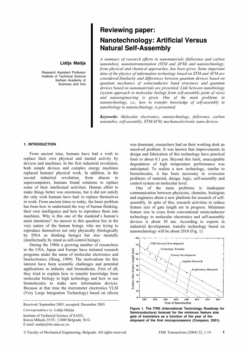
© Faculty of Mechanical Engineering, Belgrade. All rights reserved. FME Transactions (2004) 32, 1-14 1 Lidija Matija Research Assistant Professor Institute of Technical Science Serbian Academy of Sciences and Arts Reviewing paper: Nanotechnology: Artificial Versus Natural Self-Assembly A summary of research efforts in nanomaterials (fullerenes and carbon nanotubes), nanoinstrumentation (STM and AFM) and nanotechnology, from physical and chemical approaches, has been given. Some important data of the physics of information technology based on STM and AFM are considered.Similarity and differences between quantum devices based on quantum mechanics of semiconductor band structures and quantum devices based on nanomaterials are presented. Link between nanobiology (system approach to molecular biology from self-assembly point of view) and nanoengineering is given. One of the main problems in nanotechnology, i.e., how to transfer knowledge of self-assembly in nanobiology to nanotechnology, is presented. Keywords: Molecular electronics, nanotechnology, fullerenes, carbon nanotubes, self-assembly, STM/AFM, mechanoelectronic nano devices. 1. INTRODUCTION From ancient time, humans have had a wish to replace their own physical and mental activity by devices and machines. In the first industrial revolution, both simple devices and complex energy machines replaced humans' physical work. In addition, in the second industrial revolution, from abacus to supercomputers, humans found solutions to replace some of their intellectual activities. Human effort to make things better was enormous, but it did not satisfy the only wish humans have had: to replace themselves in work. From ancient times to today, the basic problem has been how to understand the way of human thinking, their own intelligence and how to reproduce them into machines. Why is this one of the mankind’s human’s main intentions? An answer to this question lies in the very nature of the human beings, who are trying to reproduce themselves not only physically (biologically by DNA as thinking beings) but also mentally (intellectually by mind as self-control beings). During the 1980s a growing number of researchers in the USA, Japan and Europe have initiated research programs under the name of molecular electronics and bioelectronics (Hong, 1989). The motivations for this interest have been scientific challenges and potential applications in industry and biomedicine. First of all, they tried to explain how to transfer knowledge from molecular biology to high technology and how to use biomolecules to make new information devices. Because at that time the micrometer electronics VLSI (Very Large Integration Technology) based on silicon was dominant, researchers had on their working desk an unsolved problem. It was known that improvements in design and fabrication of this technology have practical limit to about 0.1 µm. Beyond this limit, unacceptable degradation of high temperature performance was anticipated. To realize a new technology, similar to biomolecules, it has been necessary to overcome problems of material, design, logic, self-assembly and control system on molecular level. One of the main problems is inadequate communication between physicists, chemists, biologists and engineers about a new platform for research of self- assembly. In spite of this, research activities to reduce feature size of gate length are in progress. Minimum feature size to cross from conventional semiconductor technology to molecular electronics and self-assembly devices is about 30 nm. According to experts in industrial development, transfer technology based on nanotechnology will be about 2010 (Fig. 1). Figure 1. The ITRS (International Technology Roadmap for Semiconductors) forecast for the minimum feature size gate of transistors as a function of the year of the shipment of the first microprocessors (Compano, 2001). Received: September 2003, accepted: December 2003. Correspondence to: Lidija Matija Institute of Technical Science of SANU, Kneza Mihaila 35/IV, 11000 Belgrade, SCG E-mail: [email protected]
Transcript of Reviewing paper: Nanotechnology: Artificial Versus Natural ... · carbon cluster cage (CCC) and...
© Faculty of Mechanical Engineering, Belgrade. All rights reserved. FME Transactions (2004) 32, 1-14 1
Lidija Matija
Research Assistant Professor Institute of Technical Science
Serbian Academy of Sciences and Arts
Reviewing paper:
Nanotechnology: Artificial Versus Natural Self-Assembly A summary of research efforts in nanomaterials (fullerenes and carbon nanotubes), nanoinstrumentation (STM and AFM) and nanotechnology, from physical and chemical approaches, has been given. Some important data of the physics of information technology based on STM and AFM are considered.Similarity and differences between quantum devices based on quantum mechanics of semiconductor band structures and quantum devices based on nanomaterials are presented. Link between nanobiology (system approach to molecular biology from self-assembly point of view) and nanoengineering is given. One of the main problems in nanotechnology, i.e., how to transfer knowledge of self-assembly in nanobiology to nanotechnology, is presented. Keywords: Molecular electronics, nanotechnology, fullerenes, carbon nanotubes, self-assembly, STM/AFM, mechanoelectronic nano devices.
1. INTRODUCTION
From ancient time, humans have had a wish to replace their own physical and mental activity by devices and machines. In the first industrial revolution, both simple devices and complex energy machines replaced humans' physical work. In addition, in the second industrial revolution, from abacus to supercomputers, humans found solutions to replace some of their intellectual activities. Human effort to make things better was enormous, but it did not satisfy the only wish humans have had: to replace themselves in work. From ancient times to today, the basic problem has been how to understand the way of human thinking, their own intelligence and how to reproduce them into machines. Why is this one of the mankind’s human’s main intentions? An answer to this question lies in the very nature of the human beings, who are trying to reproduce themselves not only physically (biologically by DNA as thinking beings) but also mentally (intellectually by mind as self-control beings).
During the 1980s a growing number of researchers in the USA, Japan and Europe have initiated research programs under the name of molecular electronics and bioelectronics (Hong, 1989). The motivations for this interest have been scientific challenges and potential applications in industry and biomedicine. First of all, they tried to explain how to transfer knowledge from molecular biology to high technology and how to use biomolecules to make new information devices. Because at that time the micrometer electronics VLSI (Very Large Integration Technology) based on silicon
was dominant, researchers had on their working desk an unsolved problem. It was known that improvements in design and fabrication of this technology have practical limit to about 0.1 µm. Beyond this limit, unacceptable degradation of high temperature performance was anticipated. To realize a new technology, similar to biomolecules, it has been necessary to overcome problems of material, design, logic, self-assembly and control system on molecular level.
One of the main problems is inadequate communication between physicists, chemists, biologists and engineers about a new platform for research of self-assembly. In spite of this, research activities to reduce feature size of gate length are in progress. Minimum feature size to cross from conventional semiconductor technology to molecular electronics and self-assembly devices is about 30 nm. According to experts in industrial development, transfer technology based on nanotechnology will be about 2010 (Fig. 1).
Figure 1. The ITRS (International Technology Roadmap for Semiconductors) forecast for the minimum feature size gate of transistors as a function of the year of the shipment of the first microprocessors (Compano, 2001).
Received: September 2003, accepted: December 2003. Correspondence to: Lidija Matija Institute of Technical Science of SANU, Kneza Mihaila 35/IV, 11000 Belgrade, SCG E-mail: [email protected]
2 ▪ Vol. 32, No 1, 2004 FME Transactions
2. A SHORT HISTORY OF NANOTECHNOLOGY
For devices, in size from 0,1 nm to 500 nm, the term “molecular electronics” was more popular in the 1980s, than nanotechnology, which became more popular in the late 1990s. The term “nanotechnology” (nano: Greek-small, dwarf; science- 10-9 from basic unit in ISO system: nanometer, nanosecond, nanonewton and so on) has been proposed by Richard Feynman, the Nobel Prize winner for physics. In 1961 Feynman proposed construction of nanomachines, nanotools and nanoinstrumentation. Considering the relevance of nanotechnology to living molecules, Feynman noted, “Capabilities for atom-by-atom assembly and nanoengineering could lead to new materials and pathways similar to biological system.” The second important event for nanotechnology happened in 1981 and 1984, when Gerd Binnig and Henrich Rohrer, respectively, invented scanning tunneling microscopy (STM) and atomic force microscopy (AFM). For these inventions they won the Nobel Prize in 1986. However, the third event relevant to nanotechnology happened in 1985 and 1991, when Kroto's and Smalley's research team discovered fullerene C60, and Saumio Iijima discovered carbon nanotubes. Feynman’s concept from nanobiology to nanotechnology, Binnig-Rohrer’s invention of STM/AFM nanoinstrumentation and Kroto/Smalley-Iijima’s nanomaterial synthesis has opened the real possibilities for nanotechnology research and development. 3. NANOMATERIALS
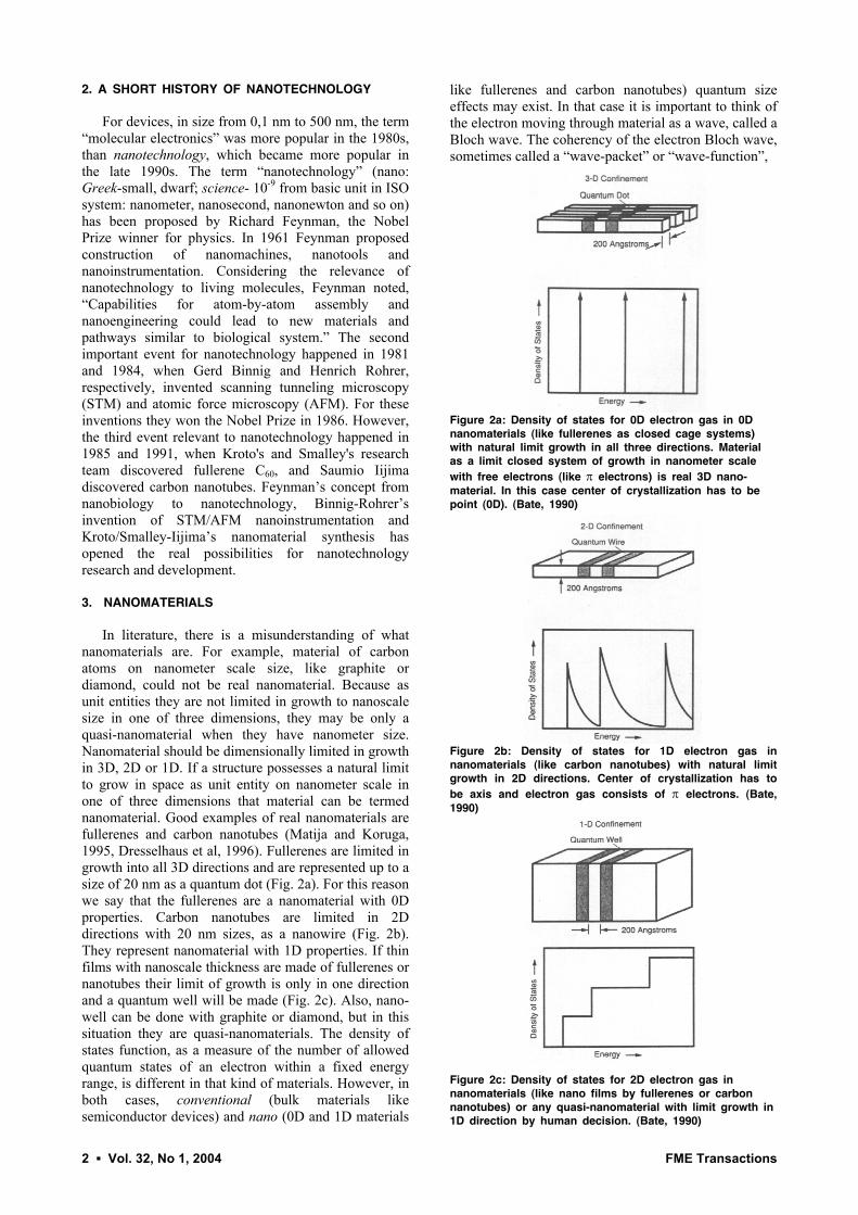
In literature, there is a misunderstanding of what nanomaterials are. For example, material of carbon atoms on nanometer scale size, like graphite or diamond, could not be real nanomaterial. Because as unit entities they are not limited in growth to nanoscale size in one of three dimensions, they may be only a quasi-nanomaterial when they have nanometer size. Nanomaterial should be dimensionally limited in growth in 3D, 2D or 1D. If a structure possesses a natural limit to grow in space as unit entity on nanometer scale in one of three dimensions that material can be termed nanomaterial. Good examples of real nanomaterials are fullerenes and carbon nanotubes (Matija and Koruga, 1995, Dresselhaus et al, 1996). Fullerenes are limited in growth into all 3D directions and are represented up to a size of 20 nm as a quantum dot (Fig. 2a). For this reason we say that the fullerenes are a nanomaterial with 0D properties. Carbon nanotubes are limited in 2D directions with 20 nm sizes, as a nanowire (Fig. 2b). They represent nanomaterial with 1D properties. If thin films with nanoscale thickness are made of fullerenes or nanotubes their limit of growth is only in one direction and a quantum well will be made (Fig. 2c). Also, nano-well can be done with graphite or diamond, but in this situation they are quasi-nanomaterials. The density of states function, as a measure of the number of allowed quantum states of an electron within a fixed energy range, is different in that kind of materials. However, in both cases, conventional (bulk materials like semiconductor devices) and nano (0D and 1D materials
like fullerenes and carbon nanotubes) quantum size effects may exist. In that case it is important to think of the electron moving through material as a wave, called a Bloch wave. The coherency of the electron Bloch wave, sometimes called a “wave-packet” or “wave-function”,
Figure 2a: Density of states for 0D electron gas in 0D nanomaterials (like fullerenes as closed cage systems) with natural limit growth in all three directions. Material as a limit closed system of growth in nanometer scale with free electrons (like π electrons) is real 3D nano-material. In this case center of crystallization has to be point (0D). (Bate, 1990)
Figure 2b: Density of states for 1D electron gas in nanomaterials (like carbon nanotubes) with natural limit growth in 2D directions. Center of crystallization has to be axis and electron gas consists of π electrons. (Bate, 1990)
Figure 2c: Density of states for 2D electron gas in nanomaterials (like nano films by fullerenes or carbon nanotubes) or any quasi-nanomaterial with limit growth in 1D direction by human decision. (Bate, 1990)
FME Transactions Vol. 32, No 1, 2004 ▪ 3
Table 1: Classification of nanomaterials, quantum structures and devices (Bate, 1990).
travels through the structure. The physical principles by which conventional semiconductor devices operate can no longer be utilized at the nanometer scale, and new physical effects must be exploited. The two most important nanotechnology mechanisms are self-assembly and quantum tunneling. An electron can pass through a potential energy barrier using tunneling effect rather than having to go over it as a classical particle. If we make quantum–coupled devices it will be possible to realise one of approaches to solve the problem of self-assembly through self-control of coupled oscillators.
Table 1 summarized the various classifications of nanomaterials, quantum structures and associative devices. Probably the major difference between real nanomaterials and quasi-nanomaterials in 3D is very limited charge capacity of the volume, for different structures made of atoms. For this reason there are two main directions in research; the first one, which uses classical semiconductor industry to produce effects of artificial quantum dots (0D), quantum wires (1D) or quantum wells (2D), and the second, which tries to produce new nanomaterial structures with 0D, 1D and 2D properties. Today, only fullerenes and carbon nanotubes possess realistic nanomaterial properties. However, the lateral motion of an electron in the lowest subband is unchanged, except for “zero-point energy” and some minor effects. For example, if the well is narrow enough, the energy required to promote an electron to the next higher subband may be much greater than its thermal energy, and it is effectively trapped in the lowest subband (Bate, 1990). This kind of situation is called the quantum limit, and through vertical degree of freedom, electrons are effectively removed to form structures like a two-dimensional electron gas. Nanodevices based on this kind of quantum effects provide the opportunity to reach minimum geometry of 10 nm and possibility to put as many as a 109 devices on a chip. However, fullerenes and carbon nanotubes can reduce size to 1 nm, and make memory devices of tera bit (1012).
3.1. Fullerenes
The fullerenes is the name of the family of carbon cluster cage molecules with 12 pentagons and different number of hexagons (C2n+20, n = 0,2,4,6, ...; n represents number of hexagons). They represent the third known crystal form of carbon, in addition to graphite and diamond. There are two main types of fullerenes:
carbon cluster cage (CCC) and carbon nanotubes (CNT). Difference between these two structures is that π electrons are oriented to the center of the cage or to point (0D) in CCC, while orientation of the same electrons are along axis (1D) in CNT. Both forms have very interesting properties owing to their structures and will be basic materials for nanotechnologies. 3.1.1. Molecule C60
Molecule C60 is the most interesting of all fullerenes. It was predicted in 1970 by Japanese scientist Osawa (Osawa, 1970) and synthesised in 1985 by Kroto/Smalley research team (Kroto et al, 1985). The first production in gram quantities of C60 was done at the University of Arizona in 1990 by Kratschmer /Hoffman team (Kratschmer at al, 1990) and its first image with atomic resolution was done at the University of Belgrade in 1992 by Koruga-Hameroff research team (Koruga et al, 1993a).
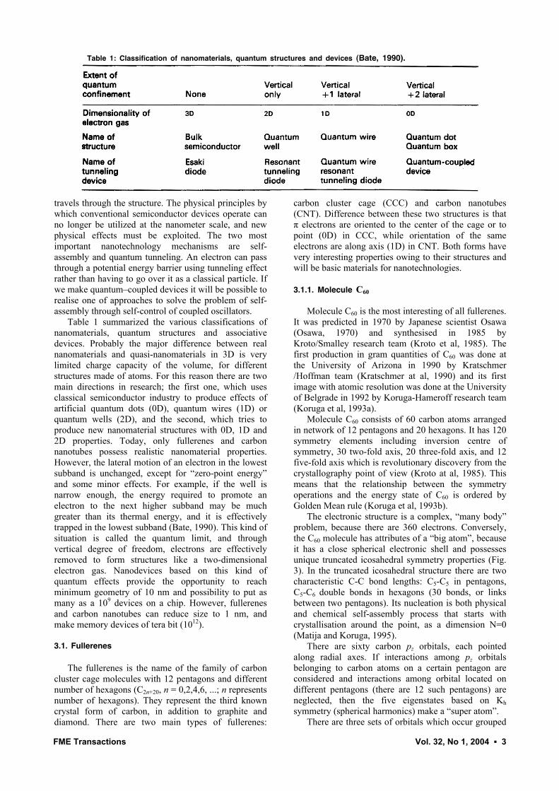
Molecule C60 consists of 60 carbon atoms arranged in network of 12 pentagons and 20 hexagons. It has 120 symmetry elements including inversion centre of symmetry, 30 two-fold axis, 20 three-fold axis, and 12 five-fold axis which is revolutionary discovery from the crystallography point of view (Kroto at al, 1985). This means that the relationship between the symmetry operations and the energy state of C60 is ordered by Golden Mean rule (Koruga et al, 1993b).
The electronic structure is a complex, “many body” problem, because there are 360 electrons. Conversely, the C60 molecule has attributes of a “big atom”, because it has a close spherical electronic shell and possesses unique truncated icosahedral symmetry properties (Fig. 3). In the truncated icosahedral structure there are two characteristic C-C bond lengths: C5-C5 in pentagons, C5-C6 double bonds in hexagons (30 bonds, or links between two pentagons). Its nucleation is both physical and chemical self-assembly process that starts with crystallisation around the point, as a dimension N=0 (Matija and Koruga, 1995).
There are sixty carbon pz orbitals, each pointed along radial axes. If interactions among pz orbitals belonging to carbon atoms on a certain pentagon are considered and interactions among orbital located on different pentagons (there are 12 such pentagons) are neglected, then the five eigenstates based on Kh symmetry (spherical harmonics) make a “super atom”.
There are three sets of orbitals which occur grouped
4 ▪ Vol. 32, No 1, 2004 FME Transactions
together: ψ0, ψ1(+,-), and ψ2(+,-). Interaction among 12 pentagons will split the twelve ψ0 orbitals to Ag + Hg + T1u + T2u, while the 24 ψ1(+, -) orbitals, two per pentagon, will split into T1g + Gg + Hg + T1u + Gu + Hu irreducible representations. The final 24 ψ2(+, -) orbitals, with the highest energy, will be split into T2g, Gu, Gg, Hu, T2u and Hg. Irreducible representations T1g, T2g, T1u and T2u for symmetry elements C5 and S10 possess Golden Mean properties: 1 2( 5 1)φ = ± − and 1 2( 5 1)Φ = ± + (Koruga et al, 1993b).
Five-fold symmetry and the Golden Mean were ignored for a long period in science, especially in crystallography. This was because of a proof of the impossibility of a 5-fold symmetry axis in a crystal medium. However, Schectman in 1984 experimentally discovered quasi-icosahedral symmetry in the alloy Al6Mn, while Penrose, from a theoretical point of view, proposed 3D tiling as five fold symmetry entities in 1989.
Figure 3: One possible Golden Mean (φ, Φ) surface energy state of molecule C60 based on mixed sixth- and tenth-rank icosahedral tensor Hamiltonians (Harter, 1989) and STM image of half molecule C60 (diameter 1 nm with surface energy state), made in 1992 at the Faculty of Mechanical Engineering, University of Belgrade (Koruga et al, 1993a).
One of the very interesting properties of fullerenes is the possibility to form three distinct types of binding sites: (1) surface - egzohedral; (2) substitutional - one or more C atoms replaced by another atom or group; and (3) endohedral-different atoms, ions, or small molecules are incorporated into fullerenes cavity (Chai et al, 1991, Dresselhaus, Dresselhaus and Eklund, 1996, Matija, 1999).
3.2. Carbon nanotubes
Carbon nanotubes (NT) are nanostructures derived from rolled graphite planes that can be closed (at the
end they have appropriate fullerene cup) or opened. One can explain physical properties of carbon nanotubes by sp2 orbital and structural properties: a diameter of tubule Dt and chiral angle θ. They can be divided into (1) single-walled (SW)-one graphite sheet and (2) multi-walled (MW)-two grapheme sheet at least (Duclaux, 2002). Single-walled nanotubes can be, also: (a) a “chiral” tubule, a general direction 0˚<θ<30˚, (b) “armchair” tubule, θ=30˚ direction, and (c) “zigzag” tubule, the θ=0˚ (Dresselhaus, Dresselhaus and Eklund, 1996).
Depending on SWNT diameter and chirality, they can be either semiconducting or metallic (Dresselhaus, et al, 2002).
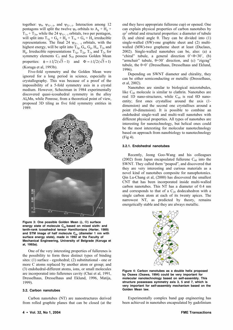
Nanotubes are similar to biological microtubules, like C60 molecule is similar to clathrin. Nanotubes are real 1D nano-structures, while C60 is real 0D nano-entity; first ones crystallise around the axis (1-dimension) and the second one crystallises around a point (0-dimension). It is possible to combine an endohedral single-wall and multi-wall nanotubes with different physical properties. All types of nanotubes are interesting for nanotechnology, but helical ones could be the most interesting for molecular nanotechnology based on approach from nanobiology to nanotechnology (Fig 4). 3.2.1. Endohedral nanotubes
Recently, Jeong Goo-Wang and his colleagues (2002) from Japan encapsulated fullerene C60 into the SWNT. They called them “peapod”, and discovered that they are very interesting and curious materials as a novel kind of nanotubes composite for nanophotonics. Qin Lu-Chang et al, (2000) has discovered the smallest CNT that has been incorporated inside multi-walled carbon nanotubes. This NT has a diameter of 0.4 nm and corresponds to that of a C20 dodecahedron with a single carbon atom at each of its twenty apices. The narrowest NT, as predicted by theory, remains energetically stable and they are always metallic.
Figure 4: Carbon nanotubes as a double helix proposed by Osawa (Osawa, 1994) could be very important for molecular nanotechnology based on self-assembly. This structure possesses symmetry axis 3, 5 and 7, which is very important for self-assembly mechanism based on the Golden Mean law.
Experimentally complex band gap engineering has been achieved in nanotubes encapsulated by gadolinium
FME Transactions Vol. 32, No 1, 2004 ▪ 5
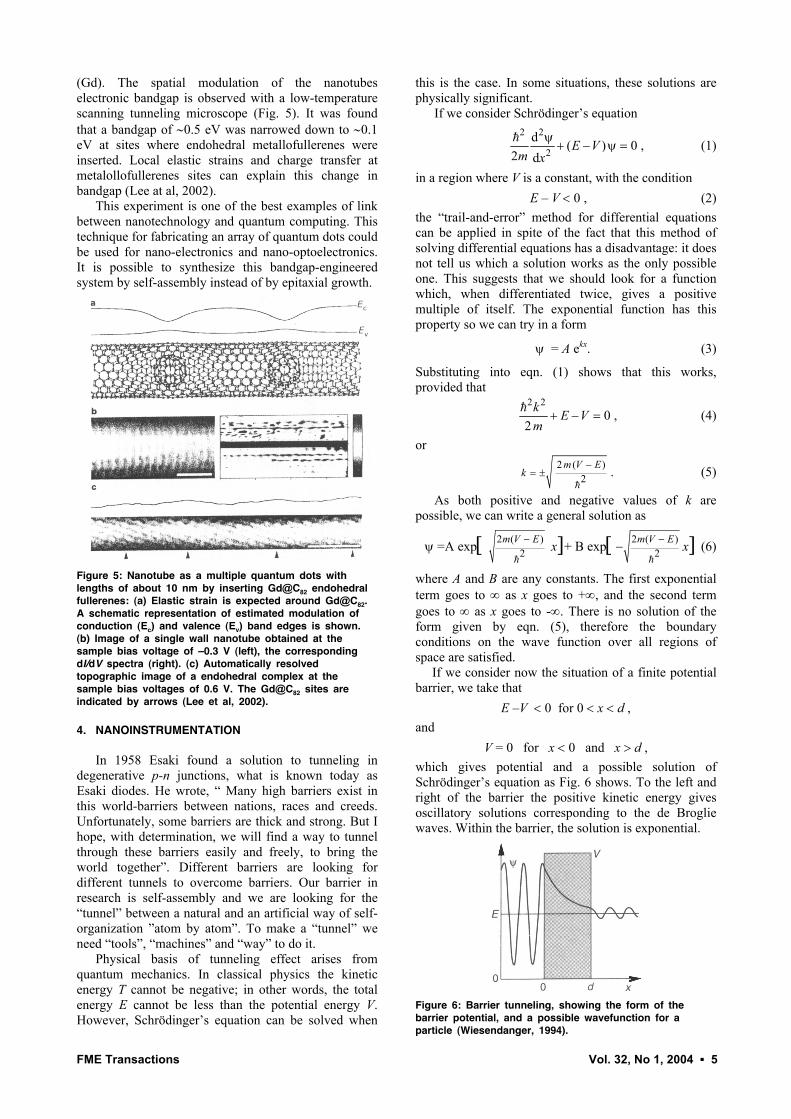
(Gd). The spatial modulation of the nanotubes electronic bandgap is observed with a low-temperature scanning tunneling microscope (Fig. 5). It was found that a bandgap of ∼0.5 eV was narrowed down to ∼0.1 eV at sites where endohedral metallofullerenes were inserted. Local elastic strains and charge transfer at metalollofullerenes sites can explain this change in bandgap (Lee at al, 2002).
This experiment is one of the best examples of link between nanotechnology and quantum computing. This technique for fabricating an array of quantum dots could be used for nano-electronics and nano-optoelectronics. It is possible to synthesize this bandgap-engineered system by self-assembly instead of by epitaxial growth.
Figure 5: Nanotube as a multiple quantum dots with lengths of about 10 nm by inserting Gd@C82 endohedral fullerenes: (a) Elastic strain is expected around Gd@C82. A schematic representation of estimated modulation of conduction (Ec) and valence (Ev) band edges is shown. (b) Image of a single wall nanotube obtained at the sample bias voltage of —0.3 V (left), the corresponding dI/dV spectra (right). (c) Automatically resolved topographic image of a endohedral complex at the sample bias voltages of 0.6 V. The Gd@C82 sites are indicated by arrows (Lee et al, 2002). 4. NANOINSTRUMENTATION
In 1958 Esaki found a solution to tunneling in degenerative p-n junctions, what is known today as Esaki diodes. He wrote, “ Many high barriers exist in this world-barriers between nations, races and creeds. Unfortunately, some barriers are thick and strong. But I hope, with determination, we will find a way to tunnel through these barriers easily and freely, to bring the world together”. Different barriers are looking for different tunnels to overcome barriers. Our barrier in research is self-assembly and we are looking for the “tunnel” between a natural and an artificial way of self-organization ”atom by atom”. To make a “tunnel” we need “tools”, “machines” and “way” to do it.
Physical basis of tunneling effect arises from quantum mechanics. In classical physics the kinetic energy T cannot be negative; in other words, the total energy E cannot be less than the potential energy V. However, Schrödinger’s equation can be solved when
this is the case. In some situations, these solutions are physically significant.
If we consider Schrödinger’s equation
2 2
2d ( ) 0
2 dE V
m xψ+ − ψ = , (1)
in a region where V is a constant, with the condition E – V < 0 , (2)
the “trail-and-error” method for differential equations can be applied in spite of the fact that this method of solving differential equations has a disadvantage: it does not tell us which a solution works as the only possible one. This suggests that we should look for a function which, when differentiated twice, gives a positive multiple of itself. The exponential function has this property so we can try in a form
ψ = A ekx. (3)
Substituting into eqn. (1) shows that this works, provided that
2 2
02
k E Vm
+ − = , (4)
or
2 ( )2
m V Ek
−= ± . (5)
As both positive and negative values of k are possible, we can write a general solution as
ψ =A exp[ 2 ( )2
m V E− x]+ B exp[ 2 ( )2
m V E−− x] (6)
where A and B are any constants. The first exponential term goes to ∞ as x goes to +∞, and the second term goes to ∞ as x goes to -∞. There is no solution of the form given by eqn. (5), therefore the boundary conditions on the wave function over all regions of space are satisfied. If we consider now the situation of a finite potential barrier, we take that
E –V < 0 for 0 < x < d , and
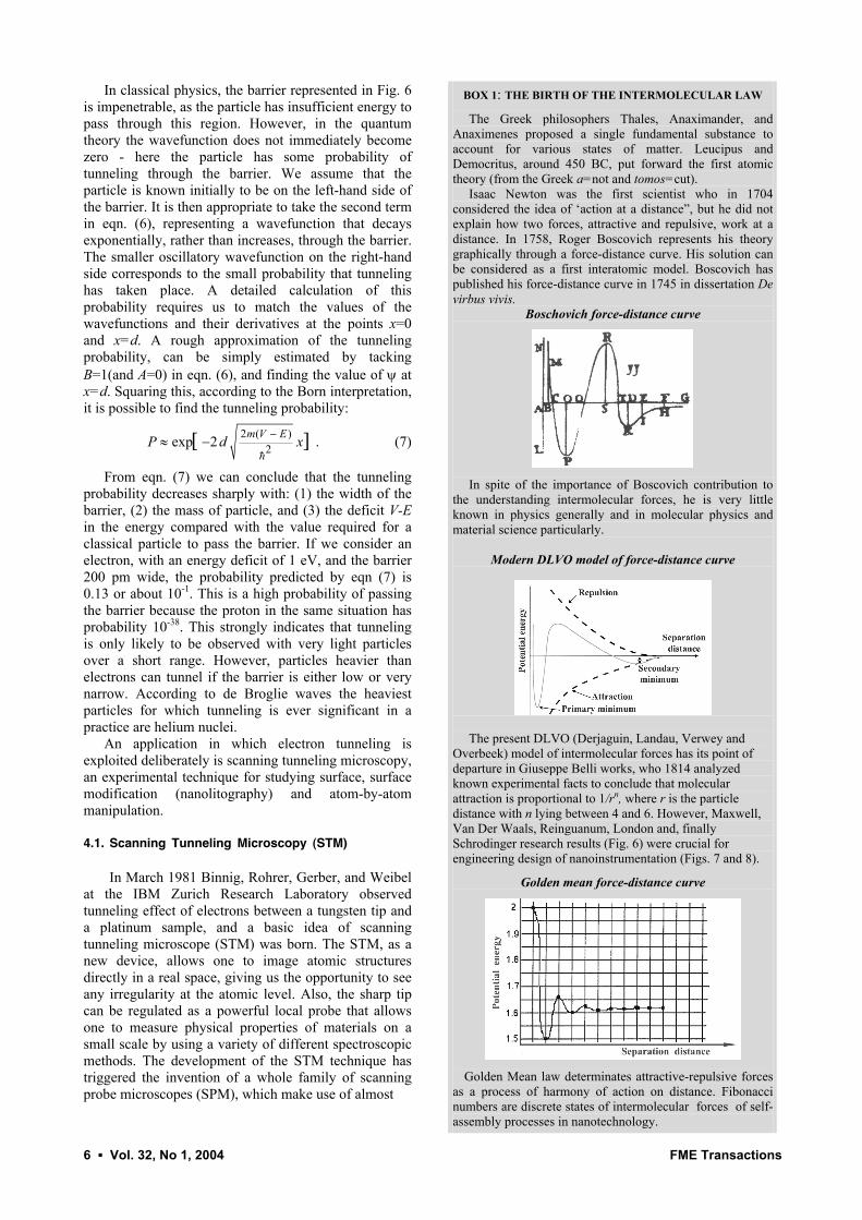
V = 0 for x < 0 and x > d , which gives potential and a possible solution of Schrödinger’s equation as Fig. 6 shows. To the left and right of the barrier the positive kinetic energy gives oscillatory solutions corresponding to the de Broglie waves. Within the barrier, the solution is exponential.
Figure 6: Barrier tunneling, showing the form of the barrier potential, and a possible wavefunction for a particle (Wiesendanger, 1994).
6 ▪ Vol. 32, No 1, 2004 FME Transactions
In classical physics, the barrier represented in Fig. 6 is impenetrable, as the particle has insufficient energy to pass through this region. However, in the quantum theory the wavefunction does not immediately become zero - here the particle has some probability of tunneling through the barrier. We assume that the particle is known initially to be on the left-hand side of the barrier. It is then appropriate to take the second term in eqn. (6), representing a wavefunction that decays exponentially, rather than increases, through the barrier. The smaller oscillatory wavefunction on the right-hand side corresponds to the small probability that tunneling has taken place. A detailed calculation of this probability requires us to match the values of the wavefunctions and their derivatives at the points x=0 and x=d. A rough approximation of the tunneling probability, can be simply estimated by tacking B=1(and A=0) in eqn. (6), and finding the value of ψ at x=d. Squaring this, according to the Born interpretation, it is possible to find the tunneling probability:
P ≈ exp[ 2 ( )22 m V Ed −
− x] . (7)
From eqn. (7) we can conclude that the tunneling probability decreases sharply with: (1) the width of the barrier, (2) the mass of particle, and (3) the deficit V-E in the energy compared with the value required for a classical particle to pass the barrier. If we consider an electron, with an energy deficit of 1 eV, and the barrier 200 pm wide, the probability predicted by eqn (7) is 0.13 or about 10-1. This is a high probability of passing the barrier because the proton in the same situation has probability 10-38. This strongly indicates that tunneling is only likely to be observed with very light particles over a short range. However, particles heavier than electrons can tunnel if the barrier is either low or very narrow. According to de Broglie waves the heaviest particles for which tunneling is ever significant in a practice are helium nuclei.
An application in which electron tunneling is exploited deliberately is scanning tunneling microscopy, an experimental technique for studying surface, surface modification (nanolitography) and atom-by-atom manipulation. 4.1. Scanning Tunneling Microscopy (STM)
In March 1981 Binnig, Rohrer, Gerber, and Weibel at the IBM Zurich Research Laboratory observed tunneling effect of electrons between a tungsten tip and a platinum sample, and a basic idea of scanning tunneling microscope (STM) was born. The STM, as a new device, allows one to image atomic structures directly in a real space, giving us the opportunity to see any irregularity at the atomic level. Also, the sharp tip can be regulated as a powerful local probe that allows one to measure physical properties of materials on a small scale by using a variety of different spectroscopic methods. The development of the STM technique has triggered the invention of a whole family of scanning probe microscopes (SPM), which make use of almost
BOX 1: THE BIRTH OF THE INTERMOLECULAR LAW
The Greek philosophers Thales, Anaximander, and Anaximenes proposed a single fundamental substance to account for various states of matter. Leucipus and Democritus, around 450 BC, put forward the first atomic theory (from the Greek a=not and tomos=cut). Isaac Newton was the first scientist who in 1704 considered the idea of ‘action at a distance”, but he did not explain how two forces, attractive and repulsive, work at a distance. In 1758, Roger Boscovich represents his theory graphically through a force-distance curve. His solution can be considered as a first interatomic model. Boscovich has published his force-distance curve in 1745 in dissertation De virbus vivis.
Boschovich force-distance curve
In spite of the importance of Boscovich contribution to the understanding intermolecular forces, he is very little known in physics generally and in molecular physics and material science particularly.
Modern DLVO model of force-distance curve
The present DLVO (Derjaguin, Landau, Verwey and Overbeek) model of intermolecular forces has its point of departure in Giuseppe Belli works, who 1814 analyzed known experimental facts to conclude that molecular attraction is proportional to 1/rn, where r is the particle distance with n lying between 4 and 6. However, Maxwell, Van Der Waals, Reinguanum, London and, finally Schrodinger research results (Fig. 6) were crucial for engineering design of nanoinstrumentation (Figs. 7 and 8).
Golden mean force-distance curve
Golden Mean law determinates attractive-repulsive forces as a process of harmony of action on distance. Fibonacci numbers are discrete states of intermolecular forces of self-assembly processes in nanotechnology.
FME Transactions Vol. 32, No 1, 2004 ▪ 7
every kind of interaction between a tip and a sample of which one can think.
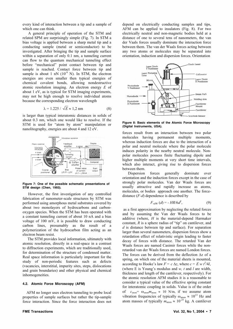
A general principle of operation of the STM and related SPM are surprisingly simple (Fig. 7). In STM a bias voltage is applied between a sharp metal tip and a conducting sample (metal or semiconductor) to be investigated. After bringing the tip and sample surface within a separation of only 0.1 nm, a tunneling current can flow to the quantum mechanical tunneling effect before “mechanical” point contact between tip and sample is reached. Contact force between tip and sample is about 1 nN (10-9 N). In STM, the electron energies are even smaller then typical energies of chemical covalent bonds, allowing nondestructive atomic resolution imaging. An electron energy E of about 1 eV, as is typical for STM imaging experiments, may not be high enough to resolve individual atoms because the corresponding electron wavelength
λ = 1.225 / E ≈ 1,2 nm (8)
is larger than typical interatomic distances in solids of about 0.3 nm, which one would like to resolve. If the STM is used for “atom by atom” manipulation or nanolitography, energies are about 4 and 12 eV.
Figure 7: One of the possible schematic presentations of STM design (Chen, 1993).
However, the first investigation of any controlled fabrication of nanometer-scale structures by STM was performed using amorphous metal substrates covered by about two monolayers of hydrocarbons and carbon-oxygen species. When the STM has been operated with a constant tunneling current of about 10 nA and a bias voltage of 100 mV, it is possible to draw conducting carbon lines, presumably as the result of a polymerization of the hydrocarbon film acting as an electron beam resist. The STM provides local information, ultimately with atomic resolution, directly in a real-space in a contrast to diffraction experiments, which are traditionally used, for determination of the structure of condensed matter. Real space information is particularly important for the study of non-periodic features such as defects (vacancies, interstitial, impurity sites, steps, dislocations and grain boundaries) and other physical and chemical inhomogeneities. 4.2. Atomic Force Microscopy (AFM) AFM no longer uses electron tunneling to probe local properties of sample surfaces but rather the tip-sample force interaction. Since the force interaction does not
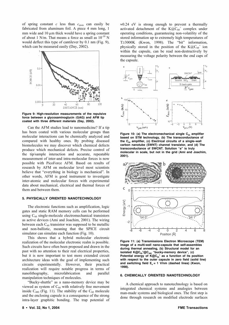
depend on electrically conducting samples and tips, AFM can be applied to insulators (Fig. 8). For two electrically neutral and non-magnetic bodies held at a distance of one to several tens of nanometers, the van der Vaals forces usually dominate the interaction force between them. The van der Waals forces acting between any two atoms or molecules may be separated into orientation, induction and dispersion forces. Orientation
Figure 8: Basic elements of the Atomic Force Microscopy (Digital Instruments, USA).
forces result from an interaction between two polar molecules having permanent multiple moments, whereas induction forces are due to the interaction of a polar and neutral molecule where the polar molecule induces polarity in the nearby neutral molecule. Non-polar molecules possess finite fluctuating dipole and higher multiple moments at very short time intervals, which also interact, giving rise to dispersion forces between them.
Dispersion forces generally dominate over orientation and the induction forces except in the case of strongly polar molecules. Van der Waals forces are usually attractive and rapidly increase as atoms, molecules, or bodies approach one another. The force-distance (F-d) dependence is described by
FvdW (d) = - HR/6d2, (9)
as a first approximation by neglecting the related forces and by assuming the Van der Waals forces to be additive (where, H is the material-depend Harmaker constant, R is a sphere radius of “tip” on cantilever, and d is distance between tip and surface). For separation larger than several nanometers, dispersion forces show a retardation effect of relativistic origin leading to faster decay of forces with distance. The retarded Van der Waals forces are named Casimir forces while the non-retarded van der Waals forces are named London forces. The forces can be derived from the deflection ∆z of a spring, on which one of the material sheets is mounted, according to Hooke’s law F = c ∆z, where c = E w t3/4l, (where Ε is Young’s modulus and w, t and l are width, thickness and length of the cantilever, respectively). For the atomic resolution AFM studies it is a reasonable to consider a typical value of the effective spring constant for interatomic coupling in solids. Value is of the order of catom= ωatommatom ≈ 10 N/m, if we assume atom vibration frequencies of typically ωatom ≈ 1013 Hz and atom masses of typically matom ≈ 10-25 kg. A cantilever
8 ▪ Vol. 32, No 1, 2004 FME Transactions
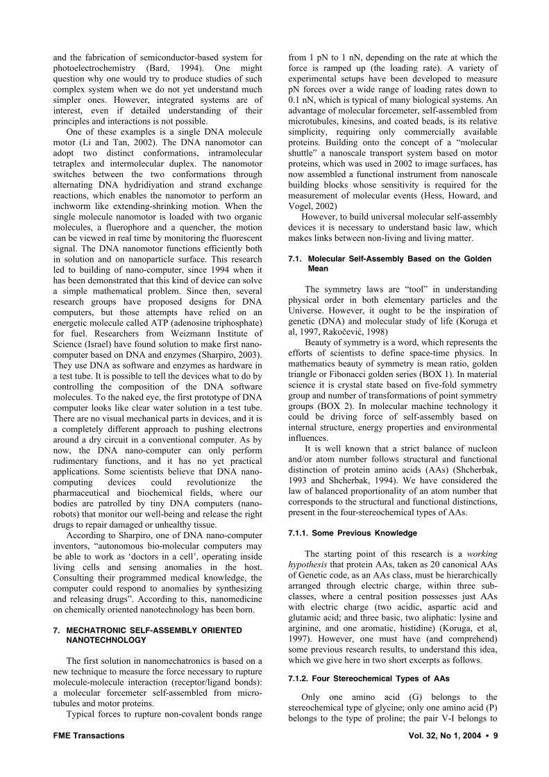
of spring constant c less than catom can easily be fabricated from aluminum foil. A piece 4 mm long, 1 mm wide and 10 µm thick would have a spring constant of about 1 N/m. That means a force as small as 10-10 N would deflect this type of cantilever by 0.1 nm (Fig. 9), which can be measured easily (Day, 2002).
Figure 9: High-resolution measurements of the repulsive force between a glycosaminoglycin (GAG) and AFM tip coated with three different materials (Day, 2002).
Can the AFM studies lead to nanomedicine? If a tip has been coated with various molecular groups than molecular interactions can be chemically analyzed and compared with healthy ones. By probing diseased biomolecules we may discover which chemical defects produce which mechanical defects. Precise control of the tip/sample interaction and accurate, repeatable measurement of inter-and intra-molecular forces is now possible with PicoForce AFM. Based on results of research by AFM on molecular level most scientists believe that “everything in biology is mechanical”. In other words, AFM is good instrument to investigate inter-atomic and molecular forces with experimental data about mechanical, electrical and thermal forces of them and between them. 5. PHYSICALLY ORIENTED NANOTECHNOLOGY
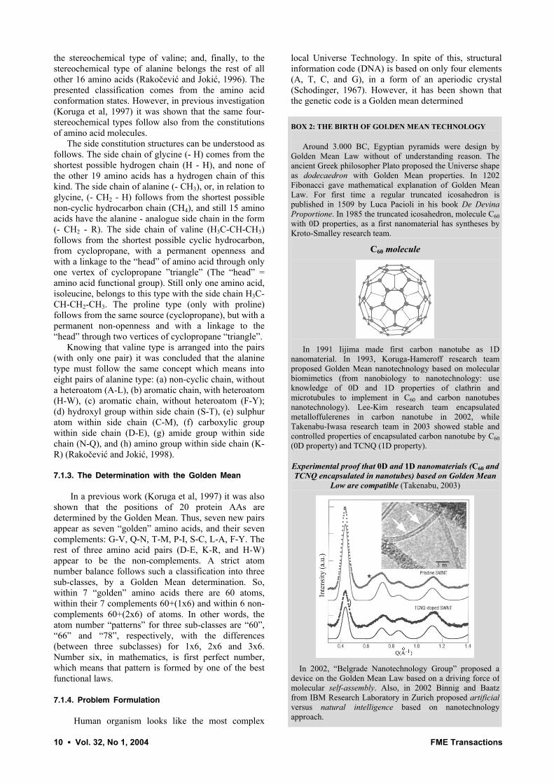
The electronic functions such as amplification, logic gates and static RAM memory cells can be performed using C60 single-molecule electromechanical transistors as active devices (Ami and Joachim, 2001). The wiring between each C60 transistor was supposed to be metallic and non-ballistic, meaning that the SPICE circuit simulator can simulate each function (Fig. 10).
This shows that a hybrid molecular electronic realization of the molecular electronic realm is possible. Such circuits have often been proposed and drawn in the past with no attention to their real electrical properties, but it is now important to test more extended circuit architecture ideas with the goal of implementing such circuits experimentally. However, their practical realization will require notable progress in terms of nanolithography, microfabrication and parallel manipulation techniques of molecules.
“Bucky-shuttle” as a nano-memory device may be viewed as system of C60 with relatively free movement inside C480 (Fig. 11). The stability of the C60 molecule and the enclosing capsule is a consequence of the strong intra-layer graphitic bonding. The trap potential of
≈0.24 eV is strong enough to prevent a thermally activated detachment of the K@C60
+ complex under operating conditions, guaranteeing non-volatility of the stored information up to extremely high temperatures of T≥3000K (Kwon, 1998). The “bit” information, physically stored in the position of the K@C60
+ ion within the capsule, can be read non-destructively by measuring the voltage polarity between the end caps of the capsule.
Figure 10: (a) The electromechanical single C60 amplifier based on STM technology, (b) The transconductance of the C60 amplifier, (c) Electrical circuits of a single—wall carbon nanotube (SWNT) channel transistor, and (d) The transconductance of SWCNT. Solution “a” is truly molecular in scale, but not in the grid (Ami and Joachim, 2001).
Figure 11: (a) Transmissions Electron Microscope (TEM) image of a multi-wall nano-capsule that self-assembles during thermal annealing, (b) Structural model for an isolated K@C60
+@C480 “bucky-memory device”, (c) Potential energy of K@C60
+ as a function of its position with respect to the outer capsule in zero field (solid line) and switching field Es = 1 V/nm (dashed lines) (Kwon, 1998).
6. CHEMICALLY ORIENTED NANOTECHNOLOGY
A chemical approach to nanotechnology is based on integrated chemical systems and analogies between man-made systems and biological ones. The first step is done through research on modified electrode surfaces
FME Transactions Vol. 32, No 1, 2004 ▪ 9
and the fabrication of semiconductor-based system for photoelectrochemistry (Bard, 1994). One might question why one would try to produce studies of such complex system when we do not yet understand much simpler ones. However, integrated systems are of interest, even if detailed understanding of their principles and interactions is not possible.
One of these examples is a single DNA molecule motor (Li and Tan, 2002). The DNA nanomotor can adopt two distinct conformations, intramolecular tetraplex and intermolecular duplex. The nanomotor switches between the two conformations through alternating DNA hydridiyation and strand exchange reactions, which enables the nanomotor to perform an inchworm like extending-shrinking motion. When the single molecule nanomotor is loaded with two organic molecules, a fluerophore and a quencher, the motion can be viewed in real time by monitoring the fluorescent signal. The DNA nanomotor functions efficiently both in solution and on nanoparticle surface. This research led to building of nano-computer, since 1994 when it has been demonstrated that this kind of device can solve a simple mathematical problem. Since then, several research groups have proposed designs for DNA computers, but those attempts have relied on an energetic molecule called ATP (adenosine triphosphate) for fuel. Researchers from Weizmann Institute of Science (Israel) have found solution to make first nano-computer based on DNA and enzymes (Sharpiro, 2003). They use DNA as software and enzymes as hardware in a test tube. It is possible to tell the devices what to do by controlling the composition of the DNA software molecules. To the naked eye, the first prototype of DNA computer looks like clear water solution in a test tube. There are no visual mechanical parts in devices, and it is a completely different approach to pushing electrons around a dry circuit in a conventional computer. As by now, the DNA nano-computer can only perform rudimentary functions, and it has no yet practical applications. Some scientists believe that DNA nano-computing devices could revolutionize the pharmaceutical and biochemical fields, where our bodies are patrolled by tiny DNA computers (nano-robots) that monitor our well-being and release the right drugs to repair damaged or unhealthy tissue.
According to Sharpiro, one of DNA nano-computer inventors, “autonomous bio-molecular computers may be able to work as ‘doctors in a cell’, operating inside living cells and sensing anomalies in the host. Consulting their programmed medical knowledge, the computer could respond to anomalies by synthesizing and releasing drugs”. According to this, nanomedicine on chemically oriented nanotechnology has been born. 7. MECHATRONIC SELF-ASSEMBLY ORIENTED
NANOTECHNOLOGY
The first solution in nanomechatronics is based on a new technique to measure the force necessary to rupture molecule-molecule interaction (receptor/ligand bonds): a molecular forcemeter self-assembled from micro-tubules and motor proteins.
Typical forces to rupture non-covalent bonds range
from 1 pN to 1 nN, depending on the rate at which the force is ramped up (the loading rate). A variety of experimental setups have been developed to measure pN forces over a wide range of loading rates down to 0.1 nN, which is typical of many biological systems. An advantage of molecular forcemeter, self-assembled from microtubules, kinesins, and coated beads, is its relative simplicity, requiring only commercially available proteins. Building onto the concept of a “molecular shuttle” a nanoscale transport system based on motor proteins, which was used in 2002 to image surfaces, has now assembled a functional instrument from nanoscale building blocks whose sensitivity is required for the measurement of molecular events (Hess, Howard, and Vogel, 2002)
However, to build universal molecular self-assembly devices it is necessary to understand basic law, which makes links between non-living and living matter. 7.1. Molecular Self-Assembly Based on the Golden
Mean The symmetry laws are “tool” in understanding
physical order in both elementary particles and the Universe. However, it ought to be the inspiration of genetic (DNA) and molecular study of life (Koruga et al, 1997, Rakočević, 1998)
Beauty of symmetry is a word, which represents the efforts of scientists to define space-time physics. In mathematics beauty of symmetry is mean ratio, golden triangle or Fibonacci golden series (BOX 1). In material science it is crystal state based on five-fold symmetry group and number of transformations of point symmetry groups (BOX 2). In molecular machine technology it could be driving force of self-assembly based on internal structure, energy properties and environmental influences.
It is well known that a strict balance of nucleon and/or atom number follows structural and functional distinction of protein amino acids (AAs) (Shcherbak, 1993 and Shcherbak, 1994). We have considered the law of balanced proportionality of an atom number that corresponds to the structural and functional distinctions, present in the four-stereochemical types of AAs.
7.1.1. Some Previous Knowledge
The starting point of this research is a working hypothesis that protein AAs, taken as 20 canonical AAs of Genetic code, as an AAs class, must be hierarchically arranged through electric charge, within three sub-classes, where a central position possesses just AAs with electric charge (two acidic, aspartic acid and glutamic acid; and three basic, two aliphatic: lysine and arginine, and one aromatic, histidine) (Koruga, et al, 1997). However, one must have (and comprehend) some previous research results, to understand this idea, which we give here in two short excerpts as follows.
7.1.2. Four Stereochemical Types of AAs
Only one amino acid (G) belongs to the stereochemical type of glycine; only one amino acid (P) belongs to the type of proline; the pair V-I belongs to
10 ▪ Vol. 32, No 1, 2004 FME Transactions
the stereochemical type of valine; and, finally, to the stereochemical type of alanine belongs the rest of all other 16 amino acids (Rakočević and Jokić, 1996). The presented classification comes from the amino acid conformation states. However, in previous investigation (Koruga et al, 1997) it was shown that the same four-stereochemical types follow also from the constitutions of amino acid molecules.
The side constitution structures can be understood as follows. The side chain of glycine (- H) comes from the shortest possible hydrogen chain (H - H), and none of the other 19 amino acids has a hydrogen chain of this kind. The side chain of alanine (- CH3), or, in relation to glycine, (- CH2 - H) follows from the shortest possible non-cyclic hydrocarbon chain (CH4), and still 15 amino acids have the alanine - analogue side chain in the form (- CH2 - R). The side chain of valine (H3C-CH-CH3) follows from the shortest possible cyclic hydrocarbon, from cyclopropane, with a permanent openness and with a linkage to the “head” of amino acid through only one vertex of cyclopropane ”triangle” (The “head” = amino acid functional group). Still only one amino acid, isoleucine, belongs to this type with the side chain H3C-CH-CH2-CH3. The proline type (only with proline) follows from the same source (cyclopropane), but with a permanent non-openness and with a linkage to the “head” through two vertices of cyclopropane “triangle”.
Knowing that valine type is arranged into the pairs (with only one pair) it was concluded that the alanine type must follow the same concept which means into eight pairs of alanine type: (a) non-cyclic chain, without a heteroatom (A-L), (b) aromatic chain, with heteroatom (H-W), (c) aromatic chain, without heteroatom (F-Y); (d) hydroxyl group within side chain (S-T), (e) sulphur atom within side chain (C-M), (f) carboxylic group within side chain (D-E), (g) amide group within side chain (N-Q), and (h) amino group within side chain (K-R) (Rakočević and Jokić, 1998). 7.1.3. The Determination with the Golden Mean
In a previous work (Koruga et al, 1997) it was also shown that the positions of 20 protein AAs are determined by the Golden Mean. Thus, seven new pairs appear as seven “golden” amino acids, and their seven complements: G-V, Q-N, T-M, P-I, S-C, L-A, F-Y. The rest of three amino acid pairs (D-E, K-R, and H-W) appear to be the non-complements. A strict atom number balance follows such a classification into three sub-classes, by a Golden Mean determination. So, within 7 “golden” amino acids there are 60 atoms, within their 7 complements 60+(1x6) and within 6 non- complements 60+(2x6) of atoms. In other words, the atom number “patterns” for three sub-classes are “60”, “66” and “78”, respectively, with the differences (between three subclasses) for 1x6, 2x6 and 3x6. Number six, in mathematics, is first perfect number, which means that pattern is formed by one of the best functional laws.
7.1.4. Problem Formulation
Human organism looks like the most complex
local Universe Technology. In spite of this, structural information code (DNA) is based on only four elements (A, T, C, and G), in a form of an aperiodic crystal (Schodinger, 1967). However, it has been shown that the genetic code is a Golden mean determined BOX 2: THE BIRTH OF GOLDEN MEAN TECHNOLOGY Around 3.000 BC, Egyptian pyramids were design by Golden Mean Law without of understanding reason. The ancient Greek philosopher Plato proposed the Universe shape as dodecaedron with Golden Mean properties. In 1202 Fibonacci gave mathematical explanation of Golden Mean Law. For first time a regular truncated icosahedron is published in 1509 by Luca Pacioli in his book De Devina Proportione. In 1985 the truncated icosahedron, molecule C60 with 0D properties, as a first nanomaterial has syntheses by Kroto-Smalley research team.
C60 molecule
In 1991 Iijima made first carbon nanotube as 1D nanomaterial. In 1993, Koruga-Hameroff research team proposed Golden Mean nanotechnology based on molecular biomimetics (from nanobiology to nanotechnology: use knowledge of 0D and 1D properties of clathrin and microtubules to implement in C60 and carbon nanotubes nanotechnology). Lee-Kim research team encapsulated metalloffulerenes in carbon nanotube in 2002, while Takenabu-Iwasa research team in 2003 showed stable and controlled properties of encapsulated carbon nanotube by C60 (0D property) and TCNQ (1D property). Experimental proof that 0D and 1D nanomaterials (C60 and TCNQ encapsulated in nanotubes) based on Golden Mean
Low are compatible (Takenabu, 2003)
In 2002, “Belgrade Nanotechnology Group” proposed a device on the Golden Mean Law based on a driving force of molecular self-assembly. Also, in 2002 Binnig and Baatz from IBM Research Laboratory in Zurich proposed artificial versus natural intelligence based on nanotechnology approach.
FME Transactions Vol. 32, No 1, 2004 ▪ 11
system (Rakočević, 1994). On the other hand, the Golden Mean is driving force of protein biomolecular machinery (Koruga et al, 1997). For nanotechnology it is important to find biomolecules (proteins) as a system whose structure and energy properties are based on the Golden Mean. Based on nanobiology knowledge we can develop new materials with self-assembled properties for molecular nanotechnology.
7.1.5. Golden Mean in Nanobiology
Clathrin and microtubules are two main proteins whose structure and energy properties are based on the Golden Mean. Clathrin was discovered in 1969 by two Japanese scientists (Kanaseki and Kadota, 1969), while microtubules, at the first time, were predicted and publ-ished by a 24-year-old Austrian cell biologist Sigmund Freud - the well known psychologist (Freud, 1882). 7.1.5.1. Clathrin
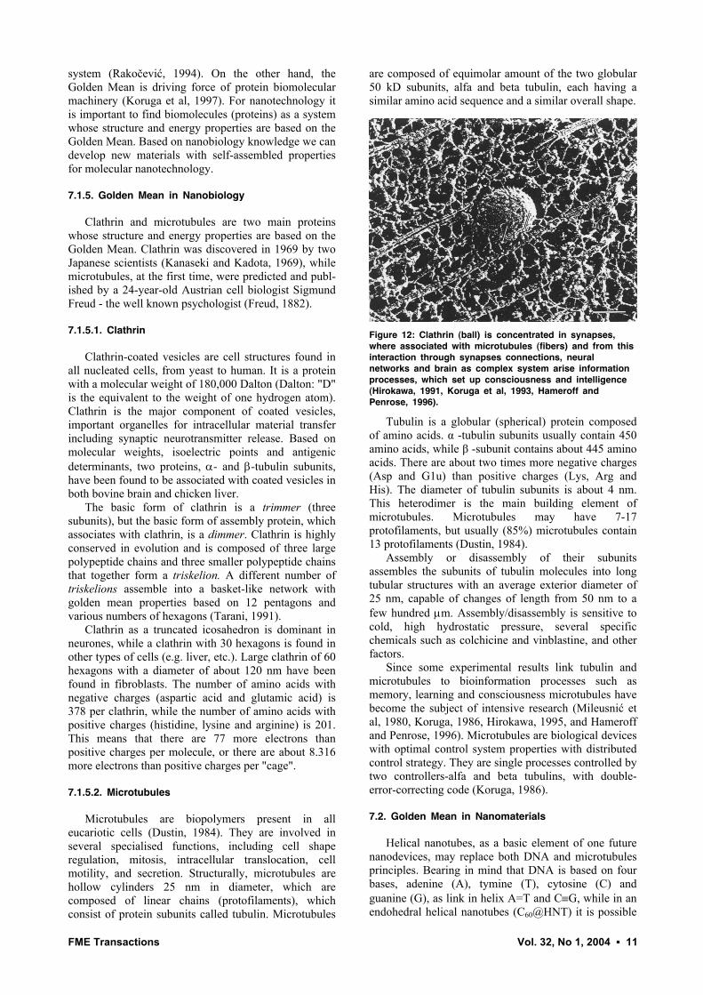
Clathrin-coated vesicles are cell structures found in all nucleated cells, from yeast to human. It is a protein with a molecular weight of 180,000 Dalton (Dalton: "D" is the equivalent to the weight of one hydrogen atom). Clathrin is the major component of coated vesicles, important organelles for intracellular material transfer including synaptic neurotransmitter release. Based on molecular weights, isoelectric points and antigenic determinants, two proteins, α- and β-tubulin subunits, have been found to be associated with coated vesicles in both bovine brain and chicken liver.
The basic form of clathrin is a trimmer (three subunits), but the basic form of assembly protein, which associates with clathrin, is a dimmer. Clathrin is highly conserved in evolution and is composed of three large polypeptide chains and three smaller polypeptide chains that together form a triskelion. A different number of triskelions assemble into a basket-like network with golden mean properties based on 12 pentagons and various numbers of hexagons (Tarani, 1991).
Clathrin as a truncated icosahedron is dominant in neurones, while a clathrin with 30 hexagons is found in other types of cells (e.g. liver, etc.). Large clathrin of 60 hexagons with a diameter of about 120 nm have been found in fibroblasts. The number of amino acids with negative charges (aspartic acid and glutamic acid) is 378 per clathrin, while the number of amino acids with positive charges (histidine, lysine and arginine) is 201. This means that there are 77 more electrons than positive charges per molecule, or there are about 8.316 more electrons than positive charges per "cage".
7.1.5.2. Microtubules
Microtubules are biopolymers present in all eucariotic cells (Dustin, 1984). They are involved in several specialised functions, including cell shape regulation, mitosis, intracellular translocation, cell motility, and secretion. Structurally, microtubules are hollow cylinders 25 nm in diameter, which are composed of linear chains (protofilaments), which consist of protein subunits called tubulin. Microtubules
are composed of equimolar amount of the two globular 50 kD subunits, alfa and beta tubulin, each having a similar amino acid sequence and a similar overall shape.
Figure 12: Clathrin (ball) is concentrated in synapses, where associated with microtubules (fibers) and from this interaction through synapses connections, neural networks and brain as complex system arise information processes, which set up consciousness and intelligence (Hirokawa, 1991, Koruga et al, 1993, Hameroff and Penrose, 1996).
Tubulin is a globular (spherical) protein composed of amino acids. α -tubulin subunits usually contain 450 amino acids, while β -subunit contains about 445 amino acids. There are about two times more negative charges (Asp and G1u) than positive charges (Lys, Arg and His). The diameter of tubulin subunits is about 4 nm. This heterodimer is the main building element of microtubules. Microtubules may have 7-17 protofilaments, but usually (85%) microtubules contain 13 protofilaments (Dustin, 1984).
Assembly or disassembly of their subunits assembles the subunits of tubulin molecules into long tubular structures with an average exterior diameter of 25 nm, capable of changes of length from 50 nm to a few hundred µm. Assembly/disassembly is sensitive to cold, high hydrostatic pressure, several specific chemicals such as colchicine and vinblastine, and other factors.
Since some experimental results link tubulin and microtubules to bioinformation processes such as memory, learning and consciousness microtubules have become the subject of intensive research (Mileusnić et al, 1980, Koruga, 1986, Hirokawa, 1995, and Hameroff and Penrose, 1996). Microtubules are biological devices with optimal control system properties with distributed control strategy. They are single processes controlled by two controllers-alfa and beta tubulins, with double-error-correcting code (Koruga, 1986).
7.2. Golden Mean in Nanomaterials
Helical nanotubes, as a basic element of one future nanodevices, may replace both DNA and microtubules principles. Bearing in mind that DNA is based on four bases, adenine (A), tymine (T), cytosine (C) and guanine (G), as link in helix A=T and C≡G, while in an endohedral helical nanotubes (C60@HNT) it is possible
12 ▪ Vol. 32, No 1, 2004 FME Transactions
from four values of the Golden Mean φ, Φ, -φ, -Φ to make links Φ-φ=1 and -Φ + φ=-1. Combination of φ, Φ, -φ, -Φ can make both, binary (1,-1) self-organisation coding system 26 = 64 and ternary (φ Φ -φ, -Φφ Φ...) self-organisation coding system 43 = 64, with one-to- Table 2: From nanobiology to molecular nanotechnology
DNA
Microtubules (MT)
Molecular nanotechnology
Nucleic acids
A T C G
A=T C≡G
Genetic code 43=64
Amino acids
Tubulin α β
Tubulin dimer in MT α-β
13,26,5
MT code 26=64
Endohedral helical nanotubes
M@C60@HNT
φ ,Φ, -φ,-Φ
1 -1
HNT code 43=64=26
one mapping. This can open possibility to make fractal computing because we can make information system based on self-similarity on different hierarchical levels. In this case artificial versus natural self-assembly may be point of departure for “artificial versus natural intelligence” (Binnig, 2002).
In 2002, “Belgrade Nanotechnology Group” on 10th Foresight conference on a molecular nanotechnology in the USA proposes one possible approach to problem solution of molecular nanotechnology based on the Golden Mean (Matija and Koruga, 2002). Basic nanomaterial is an endohedral fullerene molecule C60 in helical nanotubes (M@C60@HNT). Pulsing magnetic flux density of an endohedral nanotubes system should be by the Golden Mean. We are using knowledge from nanobiology (DNA, clathrin and microtubules) to molecular nanotechnology (based on C60 and nanotubes), in a sense of biomimicry, like as “relationship between the flight of a bird and the flight of an aircraft: both use wings but in different manners”. However, combination of molecular coding chain of spiral nanotubes (Fig. 4) with an endohedral C60 (similar to C82 in Fig. 5) will be a main structure of this molecular self-assembly nanotechnology device (see BOX 2 and Table 2). In these cases innovation inspired by nature could be model, measure and mentor for nanotechological development (Benyus, 1997). Nature as model can help us through imitation and inspiration to solve human problems in technology which using ecological standards as a measure of our industrial activities. But nature as a mentor in nanotechnology, in general, and particularly in self-assembly approach, is crucial. 8. CONCLUSION
The Golden Mean is very powerful force of self-assembly in molecular biology (DNA and proteins). It is
possible to take this knowledge from nanobiology and implement it into molecular nanotechnology. Very promising nanomaterials for self-assembly approach based on the Golden Mean in molecular nanotechnology are fullerenes and carbon nanotubes. Environment for self-assembly process should be both intelligent solvent and pulsing magnetic field by the Golden Mean.
Fullerenes and carbon nanotubes appear to be ideal candidates for nano-scale electronics and micro/nano-mechanical devices, in general, and as a nano-control device particularly.
In order for machines to be capable of intelligently pre-digesting information, they should perform in a way similar to the way humans think. Concept from a nanobiology to a nanotechnology for this kind of approach is needed. We believe that this approach can solve on-line man-machine problem in communication, in general, and open new door in the medicine (like nanomedicine) in particular. Acknowledgements
The author is grateful to Dj. Koruga for his leadership of the Molecular Machine Research Centre at the Faculty of Mechanical Engineering in Belgrade where most scientists learn about nanotechnology and have had an opportunity to conduct research using STM and AFM instrumentation since 1990. For reading this paper and giving suggestions to improve it many thanks to H. Kroto from UK, F. Hong from USA, E. Osawa, from Japan and T.A. Jung from Switzerlend. For stimulating and helpful discussion in the field of characterisation of nanomaterials, nanotechnology and Golden Mean Law I would like to thank Dj. Koruga, D. Raković, M. Rakočević, D. Uskoković and N. Romčević from Serbia. It is a pleasure to thank my teachers: Lj. Grujić, D. Debeljković, Z. Ribar, and Z. Bučevac, for their high level of education approach in the field of control systems, which help me very much for self-assembly research in nanosystems. Also, I wish to express my appreciation to MER Corporation, USA for providing fullerenes for basic research, ZEPTER INTERNATIONAL for partial research support in the field of nanotechnology under the project BIOPTRON K3 and Ministary of Scienece and Technology of Serbia, project 1431. REFERENCES 1. Ami, S., Joachim, C., 2001: Logic gates and
memory cells based on single C60 electromechanical transistors. Nanotechnology, No. 12, pp. 44-52.
2. Avramov-Ivic, M., Matija, L., Antonovic, D., Loutfy, R.O., Lowe, T., Rakin, P., Koruga, D., 2000: The Electrochemical Behaviour of Carbon Dust, Metals and Fullerenes Present in Carbon Soot. Materials Science Forum, Vol. 352, pp. 135-142.
3. Bachtold, A., Hadley, P., Nakanishi, T., Dekker, C., 2001: Logic Circuits with Carbon Nanotube transistor. Science, Vol. 294, pp. 1317-1320.
4. Bard, A. J., 1994: Integrated Chemical Systems: A Chemical Approach to Nannotechnology, John
FME Transactions Vol. 32, No 1, 2004 ▪ 13
Wiley &Sons Inc., New York. 5. Bate, R. T., 1990: Nanoelectronics. Nanotechno-
logy, No. 1, pp. 1-7. 6. Benyus, J.M., 2002: Biomimicry: Innovation
inspired by nature, Perennial, New York. 7. Binning G., Baaty M., Klenk J., Schmidt G., 2002:
Will machines start to think like humans?; Artificial versus natural Intelligence. Europhysics news, March/April, pp. 44-47.
8. Bogunia-Kubik, K., Sugisaka, M., 2002: From molecular biology to nanotechnology and nanomedicine. BioSystems, Vol. 65, pp. 123-138.
9. Compañó R., 2001: Trends in nanoelectronics. Nanotechnology, No. 12, pp. 85-88.
10. Cooper, E.B., Manalis, S.R., Fang, H., Dai, H., Matsumoto, K., Minne, S.C., Hunt, T., Quate, C.F., 1999: Terabit-per-square-inch data storage with the atomic force microscope. Applied Physics Letters, Vol. 75, No. 22.
11. Day, C., 2002: Probing the Nanomechanics of Cartilage with Atomic Force Microscopy. Physics Today, No.9, pp.21-23.
12. Dequesnes, M., Rotkin, S.V., Aluru, N. R., 2002: Calculation of pull-in voltages for carbon-nanotube-based nanoelectromechanical switches. Nanotechnology, No. 13, pp. 120-131.
13. Dresselhaus M.S., Dresselhaus G., Eklund P.C., 1996: Science of Fullerenes and Carbon Nanotubes, Academic Press, San Diego.
14. Dresselhaus, M.S., Dresselhaus, G., Jorio, A., Souza Filho, A.G., Saito, R., 2002: Raman spectroscopy on isolated single wall carbon nanotubes. Carbon, Vol. 40, pp. 2043-2061.
15. Duclaux, L., 2002: Review of the doping of carbon nanotubes (multi-walled and single-walled). Carbon, Vol. 40, pp. 1751-1764..
16. Dustin, P., 1984: Microtubules, 2nd Revised Ed, Springer, Berlin.
17. Freud, S., Sitzungsber., D., Wiener, A., 1882: Math-nat., Cl. 85, pp. 9.
18. Girard, P., 2001: Electrostatic force microscopy: principles and some applications to semiconductors. Nanotechnology, No. 12, pp. 485-490.
19. Haberzettl, C. A, 2002: Nanomedicine: destination or journey?. Nanotechnology, No.13, pp. R9-R13.
20. Haken, H., 1988: Information and Self-organization, Springer-Verlag, Berlin.
21. Hameroff, S. Penrose, R., 1996: Orchestrated reduction of quantum coherence in brain micro-tubules: a model for consciousness, in Toward of a Science of Consciousness, MIT Press, pp.507-540.
22. Harter, W.G., Weeks, D.E., 1989:Rotation-vibration spectra of icosahedral molecules. J. Chem. Phys., Vol. 90, No.9, pp. 4724-4743.
23. Hess, H., Howard, J., Vogel ,V., 2002: A PicoNewton Forcemeter Assembled from Microtubules and Kinesins. Nano Letters, Vol.2, No.10, pp. 1113-1115.
24. Hong, F, 1989: Molecular electronics: Biosensors and Biocoputers, Plenum Press, New York.
25. Hirokawa, N., 1991: The Neuronal Cytoskeleton, edited R. D. Burgoyne, Wiley Press, pp.5.
26. Iijima, S., 1991: Helical microtubules of graphitic carbon. Nature, Vol. 354, pp.56-59.
27. Ivetic, M., Mojovic, Z., Matija, L., 2003: Electrical Conductivity of Fullrenes Derivates. Materials Science Forum, Vol. 413, pp.49-52.
28. Kaneski, T., Kadota, K., 1969: The “vescile in a basket”. J.Cell Biology, Vol. 20, pp. 202-220,
29. Komatsu, K., Wang, G.-W., Murata, Y., Tanaka, T., Fujuwara, K., 1998: Mechanochemical Synthesis of the Fullerene Dimer C120. J. Org. Chem., Vol. 63, pp. 9358-9366.
30. Koruga, D., 1986: Microtubule screw symmetry: Packing of spheres as a latent bioinformation code. Ann. N.Y. Acad. Sci., Vol. 466, pp. 953-955.
31. Koruga, D., Simic-Krstic, J, Trifunovic, M., Jankovic, S., Hameroff, S., Withers J., Loutfy, R. 1993a: Imaging fullerene C60 with atomic resolution using a scanning tunnelling microscope. Fullerene Science and Technology, Vol. 1, No. 1, pp. 93-100.
32. Koruga, D., Hameroff, S., Withers J., Loutfy, R. and Sundareshan, M, 1993b: Fullerene C60: History, Physics, Nanobiology, Nanotechnology, North-Holland, Amsterdam.
33. Koruga, D., Rakocevic, M, Misic, N, Matija, L, Jankovic, S, 1997: A new classification of protein amino acids by module 3/2. Archive of Oncology, Vol. 5, No.3, pp. 137-138.
34. Koruga, D., Simic-Krstic, J., 1988: Semiconductor and crystal symmetry assessment of microtubule proteins as molecular machines. J. Mol. Elec., Vol.6, pp. 167-173.
35. Koruga, D., Matija, L., Misic, N., Rakin, P., 1996: Fullerene C60: Properties and Possible Applications. Materials Science Forum, Vol. 214 pp. 49-56.
36. Kroto, H.W., Heath, J.R., O’Brien, S.C.O., Curl, R.F., Smalley, R.E., 1985: C60 Buckminserfullerene Nature, Vol. 318, pp. 162-163.
37. Kratschmer, W., Lamb, L.D., Fostiropoulos, K., Huffman, D.R., 1990: Solid C60: A new form of carbon. Nature, Vol. 347, pp.354-358.
38. Kwon, Y.K.K., Tománek, D., Iijima, S., 1998: Synthesis and modelling of a nanotube-based memory device. J. Mater. Res., Vol. 13, pp. 2363-2367.
39. Lee, J., Kim, H., Kahng, S.-J., Kim, G., Son Y.-W., Ihm, J., Kato, H., Wang, Z.W., Okazaki, T., Shinohara, H., Kuk, Y., 2002: Bandgap modulation of carbon nanotubes by encapsulated metallofullerenes. Letters to Nature, Vol. 415, pp. 1005-1008.
40. Li, J.J., Tan, W., 2002: A Single DNA Molecule Nanomotor. Nano Letters, Vol. 2, No. 4, pp. 315-318.
41. Matija, L., 2000: Endohedral Fullerenes, Zadužbina Andrejevic, Belgrade.
14 ▪ Vol. 32, No 1, 2004 FME Transactions
42. Matija, L., 2003: Nanotechnology based on the fullerens and carbon nanotubes. Tehnika: Novi Materijali, Vol. 12, No. 2, pp. 1-18.
43. Matija, L., Koruga, D., 1995: Phenomena of crystallization around the point and molecule C60 synthesis. Tehnika, Vol. 4, No. 7-8, pp. 21-27.
44. Matija, L., Koruga,D., 2002: Golden Mean as a driving Force of Molecular Self-assembly. 10th Foresight Conference on Molecular nanotechnology, Bethseda, USA, pp.32.
45. Matija L., Koruga, D., 1998: New Materials Based on endohedral Fullerenes: Mo@C60 Complex. Materials Science Forum, Vol. 282-283, pp.115-122.
46. Matija, L., Avramov-Ivic, M., Kapetanovic, V., 2003: Different Aspects of Electrochemical Investigations of Carbon Soot Containing Endohedral Fullerenes and C60 Molecules in Natural and Alkaline Electrolytes. Materials Science Forum, Vol. 413, pp.53-58.
47. Matija, L., Koruga, D., 1994: Optimal Control and Self-Assembly of Fullerenes. Proc. Materials Research Society USA, Boston, USA, p p.60.
48. Mileusnic, R., Rose, S.P., Tillson, P., 1980: Passive avoidance learning resulting the chick forebrain. Neural Chemistry, Vol. 34, pp. 1007.
49. Qin, L.-C., Zhao, X., Hirahara, K., Miyamoto, Y., Ando, Y., Iijima, S., 2000: The smallest carbon nanotube. Nature, Vol. 408, pp. 50.
50. Osawa, E, 1970: Truncated eicosahedron. Kagaku (Kyoto) , No. 25, pp. 854.
51. Osawa, E, Yoshida, M., Fujita, M., 1994: Shape and Fantasy of Fullerenes. MRS Bulletin, Vol.XIX, No.11, pp. 33-36.
52. Rakocevic, M., 1998: The genetic code as a Golden mean determined system. BioSystems, No. 46, pp. 283-291.
53. Rakocevic, M. M, Jokic, A, 1996: Four Stereochemical Types of Amino Acids. J. Theor. Biol, Vol. 183, pp. 345-349.
54. Shorpio, A., 2003: DNA programmable molecular computing machine. Proc. of the National Acad-emy of Sciences, USA, on line edition, Feb. 24.
55. Shcherbak, V. I., 1993: Sixty-four triplets and 20 canonical amino acids of the genetic code: the arithmetical regularities. Part I. J Theor. Biol., Vol. 162, pp. 399-402.
56. Shcherbak, V.I, 1994: Sixty-four triplets and 20 canonical amino acids of the genetic code: the arithmetical regularities. Part II. J Theor. Biol., Vol. 166, pp. 475-477.
57. Schrodinger, E, 1967: What is Life? & Mind and Matter, Cambridge University Press.
58. Tsu, R., 2001: Challenges in nanoelectronics. Nanotechnology, No. 12, pp. 656-628.
59. Takenobu, T., Takano, T., Shiraishi, M., Murakami, M., Ata, M., Kataura, H., Achiba, Y., Iwasa,Y., 2003: Stable and controlled amphoteric doping by encapsulation of organic molecules inside carbon nanotubes. Nature Materials, Vol. 2, pp. 683-688.
60. Wills, R.P., 1993: Self-organization of genetic coding. J.Theor. Biology, Vol. 162, pp. 267-287.
НАНОТЕХНОЛОГИЈА:
ВЕШТАЧКА НАСПРАМ ПРИРОДНЕ САМОРГАНИЗАЦИЈE МАТЕРИЈЕ
Лидија Матија
У раду је дат приказ развоја наноматеријала
(фулерена и угљеничних нанотуба), наноинструме-нтације (СТМ и АФМ) и нанотехнологија, како са физичког тако и са хемијског аспекта. У раду су разматрани важни подаци за разбој информационих технологија, добијени помоћу СТМ и АФМ. Дат је приказ сличности и разлика између квантних уређаја заснованих на квантној механици полупроводничких трака и квантној механици наноматеријала. У раду је такође дата веза између нанобиологије (приказ молекуларно-биолошких система са аспекта самоорганизације) и наноинже-њерства. Посебно је дискутован један од главних проблема у нанотехнологији, а то је проблем преноса знања из нанобиологије који се односи на самоорганизацију материје и процеса.