Review of Power Electronic Device Models - Keysight · Review of Power Electronic Device Models ...
31
Review of Power Electronic Device Models <Your Name> EEsof EDA September, 2014
Transcript of Review of Power Electronic Device Models - Keysight · Review of Power Electronic Device Models ...

Review of Power Electronic Device Models
<Your Name>
EEsof EDA
September, 2014

Page
Power Electronics: Diverse Application Space
Power Device Models 2
Page
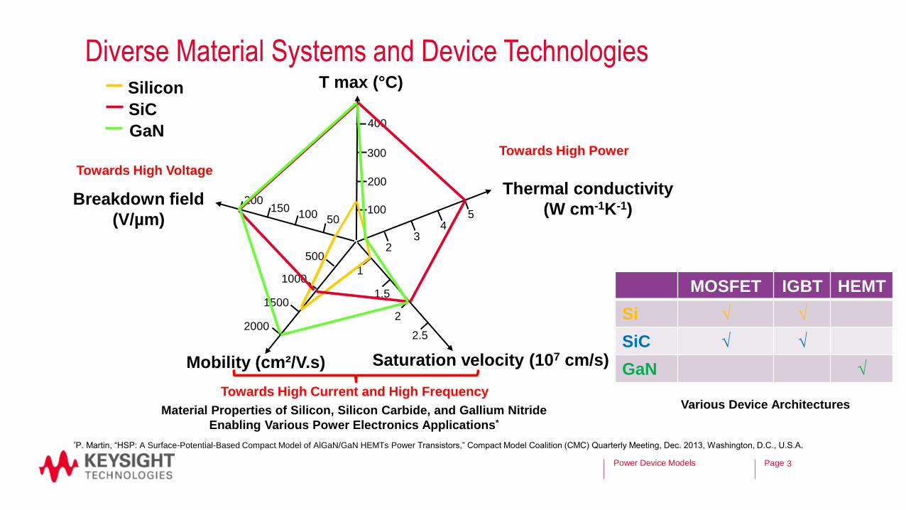
Diverse Material Systems and Device Technologies
Power Device Models 3
*P. Martin, “HSP: A Surface-Potential-Based Compact Model of AlGaN/GaN HEMTs Power Transistors,” Compact Model Coalition (CMC) Quarterly Meeting, Dec. 2013, Washington, D.C., U.S.A.
Material Properties of Silicon, Silicon Carbide, and Gallium Nitride
Enabling Various Power Electronics Applications*
MOSFET IGBT HEMT
Si √ √
SiC √ √
GaN √
Various Device Architectures
Thermal conductivity
(W cm-1K-1)
Mobility (cm²/V.s) Saturation velocity (107 cm/s)
T max (°C)
Breakdown field
(V/µm)100
200
300
400
50100150
200
23
54
1
1.5
2
2.52000
1500
1000
500
Silicon
SiC
Towards High Current and High Frequency
GaNTowards High Power
Towards High Voltage
Page
Datasheets and Behavioral Models
– Datasheets
• Device ratings (ex. maximum voltage, current, power, temperature, etc.)
• Key static characteristics
• Key dynamic characteristics
• Output/transfer curves
• Other circuit characteristics (ex. switching energy, delays, etc.)
• Thermal/mechanical characteristics
– Behavioral models
• Usually built based on and reflects datasheet information
• Usually valid for specific conditions
Power Device Models 4

Page
Needs for More Advanced Models
– Wider and more continuous coverage: bias conditions, operating temperature, various
load conditions
– More efficient circuit design and optimization
– Electro-thermal simulation to account for self-heating
– Consideration of other device characteristics (ex., noise)
– Consideration of unique device-level phenomena (ex., dynamic RON, drain lag)
– Analysis of process variations and corners
– Predictive ability for application-driven process improvement
Power Device Models 5
PageOutline
– Device models for silicon HV MOS transistors, silicon
IGBTs, SiC MOSFETs, and SiC IGBTs
– Device models for GaN HEMTs
– Summary
6Power Device Models

Page
Silicon High-Voltage MOSFET
– Symmetric high-voltage MOSFET or asymmetric laterally double-diffused MOS
(LDMOS) transistors
Power Device Models 7
*W. Yao, et all., ‘SP-HV: A scalable surface-potential-based compact model for LDMOS transistors,’ IEEE T-ED, vol. 59, no. 3, Mar. 2012, pp. 542-550
𝑉𝐷 = 3,6,9,12𝑉
Cross-section of an LDMOS Transistor* Output I-V Characteristics* Total Gate Capacitance*

Page
Silicon HV/LDMOS Models
– Sub-circuit based approaches
– HiSIM_HV: CMC industry standard model for
HV/LD MOS
Power Device Models 8
*E. Seebacher, et al., ‘High voltage MOSFET modeling,’ in Compact Modeling: Principles, Techniques and Applications, G. Gildenblat, Ed. New York: Springer-Verlag, 2010, ch. 4, pp. 105–136.†H.J. Mattausch, et al., ‘The Second-Generation of HiSIM_HV Compact Models for High-Voltage MOSFETs,’ IEEE T-ED, vol. 60, no. 2, Feb. 2013, pp. 653-661.
Typical Sub-Circuit Topology for LDMOS
Models*
Surface-Potential-Based
Approach in HiSIM_HV†
Major Recent Improvements in
HiSIM_HV†

Page
Silicon Insulated-Gate Bipolar Transistor (IGBT)
Power Device Models 9
*A.R. Hefner, ‘Device Models, Circuit Simulation, and Computer-Controlled Measurements for the IGBT,’ Proc. IEEE Workshop Computers in Power Electronics, Aug. 1990, pp. 233-243.
Cross-Section of One-Half of a Symmetric IGBT Cell*
GateEmitter
Collector
Page
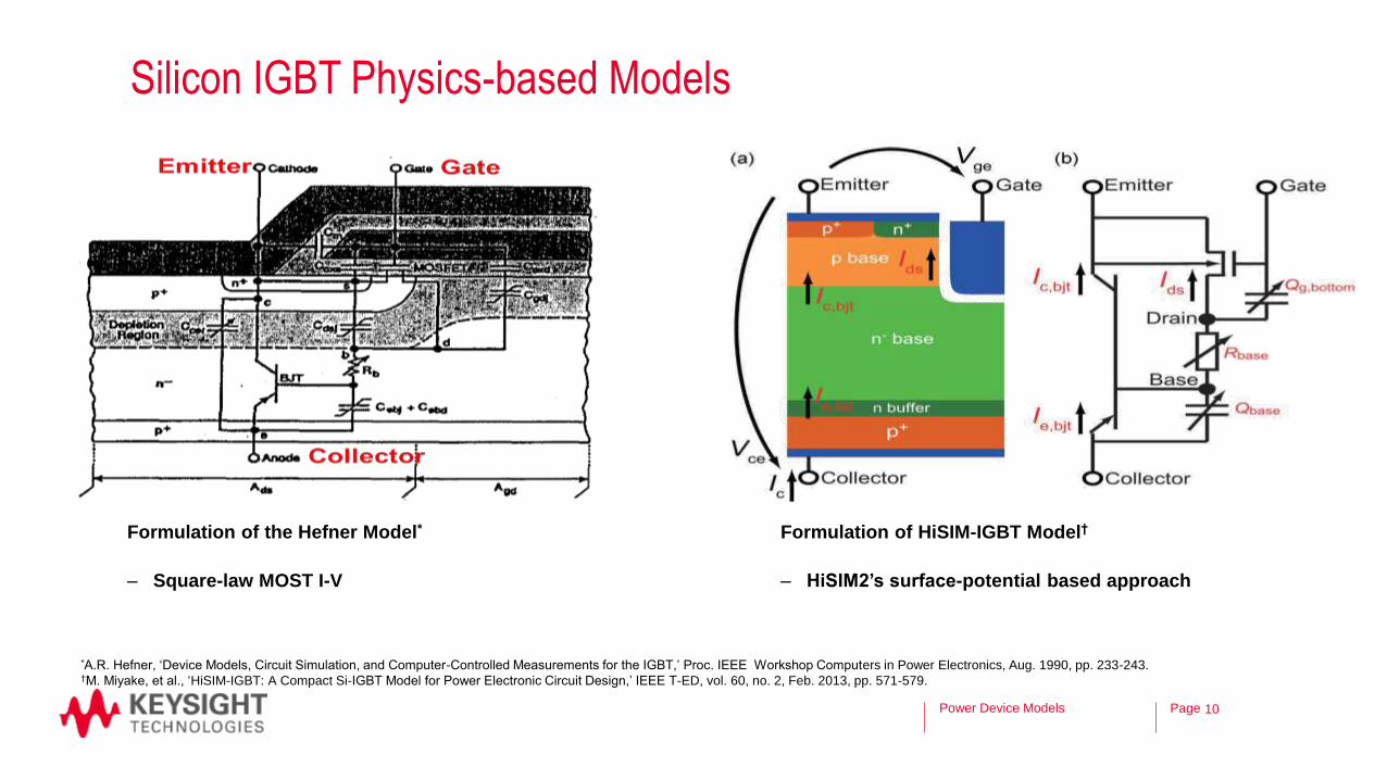
Silicon IGBT Physics-based Models
Power Device Models 10
*A.R. Hefner, ‘Device Models, Circuit Simulation, and Computer-Controlled Measurements for the IGBT,’ Proc. IEEE Workshop Computers in Power Electronics, Aug. 1990, pp. 233-243.†M. Miyake, et al., ‘HiSIM-IGBT: A Compact Si-IGBT Model for Power Electronic Circuit Design,’ IEEE T-ED, vol. 60, no. 2, Feb. 2013, pp. 571-579.
Formulation of the Hefner Model*
– Square-law MOST I-V
Formulation of HiSIM-IGBT Model†
– HiSIM2’s surface-potential based approach

Page
SiC MOSFET Models
– University of Arkansas model*
• Based on the MOSFET portion of the Hefner IGBT
model
• Two parallel MOSFETs to account for corner conduction
• Bias-dependent gate-drain overlap capacitance
• Temperature dependent material properties of SiC
implemented
– The Angelov model†
• Empirical fitting by accurately capturing key
characteristics
• SiC-specific numerical function used in I-V formulation
Power Device Models 11
*T.R. McNutt, et al., ‘Silicon Carbide Power MOSFET Model and Parameter Extraction Sequence,’ IEEE T-PE, vol. 22, no. 2, Mar. 2007, pp. 353-363.†I. Angelov, ‘Compact, Equivalent Circuit Models for GaN, SiC, GaAs and CMOS FET,’ MOS-AK, Baltimore, MD, 2008.
Cross-Section of a SiC DiMOSFET*

Page
SiC IGBT Model
– University of Arkansas model§
• Based on the Hefner model
• Adopts the enhancements of UA SiC MOSFET model
• Updated SiC mobility high-field degradation model
– HiSIM-SiC-IGBT model†
• Based on HiSIM-IGBT model for silicon
• Updated model parameters to SiC material properties
• Detailed treatment of base carrier distribution including the
punch-through effect for improved turn-off behavior modeling
Power Device Models 12
*S.H. Ryu, et al., ‘Ultra High Voltage (>12 kV), High Performance 4H-SiC IGBTs,’ Proc. IEEE IS-PSDIC, June 2012, Bruges, Belgium, pp. 257-260.§M. Saadeh, et al., “A unified silicon/silicon carbide IGBTmodel,” in Proc. IEEE Appl. Power Electron. Conf. Expo., 2012, pp. 1728–1733.†M. Miyake, et al., ‘Modeling of SiC IGBT Turn-off Behavior Valid for Over 5-kV Circuit Simulation,’ IEEE T-ED, vol. 60, no. 2, Feb. 2013, pp. 622-629.
Cross-Section of a) SiC P-IGBT, and b) SiC N-
IGBT*
a)
b)

PageOutline
– Device models for silicon HV MOS transistors, silicon IGBTs,
SiC MOSFETs, and SiC IGBTs
– Device models for GaN HEMTs
• Candidate models for CMC standardization
• DynaFET model
– Summary
13Power Device Models

Page
GaN HEMT Model Standardization Effort in CMC
– Compact Model Coalition* – an industry body that standardizes and promotes SPICE models for semiconductor
devices as well as compiled modeling interface
• Ex., standard models for silicon MOSFETs, BJTs, resistors, varactors, junction diodes
– Dedicated workgroup for GaN HEMT model standardization launched in Year 2011
– Three-phase standardization process
• Phase I: completed
- Solicitation of models and presentation to CMC
• Phase II: on-going
- Shortlisted candidate models being examined against fundamental requirements and being fitted to
measurement data for CMC evaluation
• Phase III: TBD
- Evaluation on runtime, convergence, operability, etc.
• Balloting for standardization
Power Device Models 14
*Compact Model Coalition, https://www.si2.org/cmc_index.php

Page
Candidate Models
– Requirements for the core model
• As exact, complete, and simple a representation of physical GaN HEMT behavior as possible
• Extensibility of the model from GaN to all III-V FET/HEMT structures would be an added
benefit but is not a strict requirement
• Physically correct in all operating regions
• No unphysical behavior
• As computationally efficient as possible
• Model should be charge based and not capacitance based, and charge conserving
– Candidate models entering Phase II evaluation
• Angelov-GaN model (Chalmers Univ.); COMON model (URV); HSP model (Leti); MVSG-HV
model (MIT);
Power Device Models 15

Page
Angelov-GaN Model
– Extended from the Angelov model – an empirical equivalent
circuit based model for GaAs HEMT
• Continues to use inflection points as model parameters
• New math function for I-V formulation
• New RC delay circuit in the equivalent circuit for knee
walkout
• Charge based mode in addition to conventional
capacitance only approach
• ..
Power Device Models 16
†I. Angelov, ‘Compact, Equivalent Circuit Models for GaN, SiC, GaAs and CMOS FET,’ MOS-AK, Baltimore, MD, 2008.
Illustration of Using Inflection Points as Model
Parameters in the Angelov-GaN Model†
Page
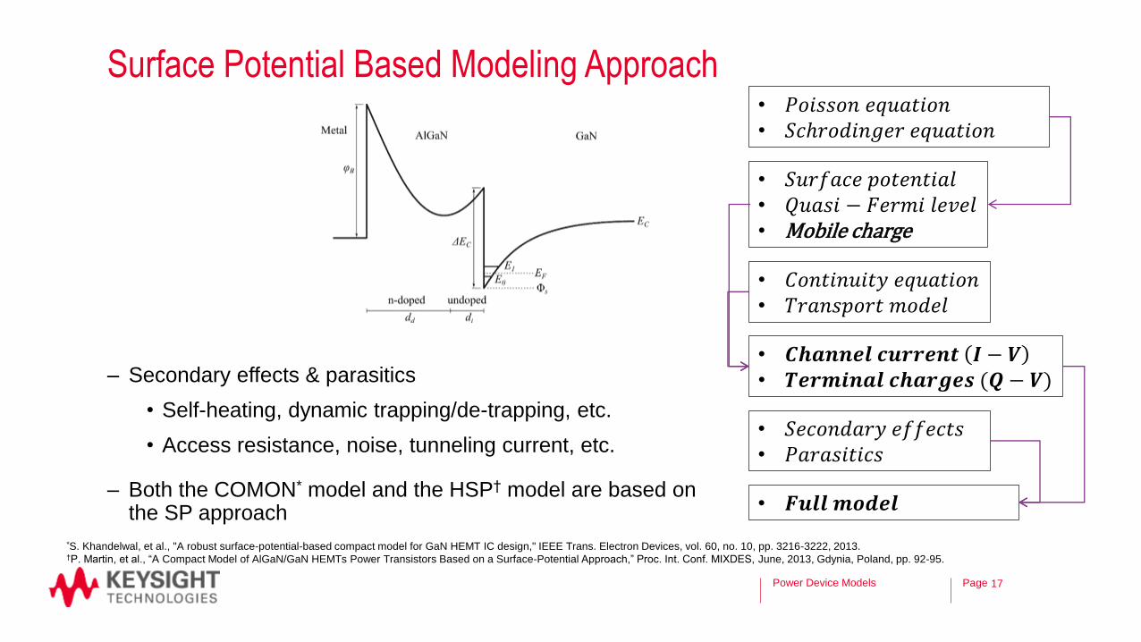
Surface Potential Based Modeling Approach
– Secondary effects & parasitics
• Self-heating, dynamic trapping/de-trapping, etc.
• Access resistance, noise, tunneling current, etc.
– Both the COMON* model and the HSP† model are based on the SP approach
17
• 𝑃𝑜𝑖𝑠𝑠𝑜𝑛 𝑒𝑞𝑢𝑎𝑡𝑖𝑜𝑛• 𝑆𝑐ℎ𝑟𝑜𝑑𝑖𝑛𝑔𝑒𝑟 𝑒𝑞𝑢𝑎𝑡𝑖𝑜𝑛
• 𝑆𝑢𝑟𝑓𝑎𝑐𝑒 𝑝𝑜𝑡𝑒𝑛𝑡𝑖𝑎𝑙• 𝑄𝑢𝑎𝑠𝑖 − 𝐹𝑒𝑟𝑚𝑖 𝑙𝑒𝑣𝑒𝑙• Mobile charge
• 𝐶𝑜𝑛𝑡𝑖𝑛𝑢𝑖𝑡𝑦 𝑒𝑞𝑢𝑎𝑡𝑖𝑜𝑛• 𝑇𝑟𝑎𝑛𝑠𝑝𝑜𝑟𝑡 𝑚𝑜𝑑𝑒𝑙
• 𝑪𝒉𝒂𝒏𝒏𝒆𝒍 𝒄𝒖𝒓𝒓𝒆𝒏𝒕 𝑰 − 𝑽• 𝑻𝒆𝒓𝒎𝒊𝒏𝒂𝒍 𝒄𝒉𝒂𝒓𝒈𝒆𝒔 (𝑸 − 𝑽)
• 𝑆𝑒𝑐𝑜𝑛𝑑𝑎𝑟𝑦 𝑒𝑓𝑓𝑒𝑐𝑡𝑠• 𝑃𝑎𝑟𝑎𝑠𝑖𝑡𝑖𝑐𝑠
• 𝑭𝒖𝒍𝒍 𝒎𝒐𝒅𝒆𝒍
*S. Khandelwal, et al., "A robust surface-potential-based compact model for GaN HEMT IC design," IEEE Trans. Electron Devices, vol. 60, no. 10, pp. 3216-3222, 2013. †P. Martin, et al., “A Compact Model of AlGaN/GaN HEMTs Power Transistors Based on a Surface-Potential Approach,” Proc. Int. Conf. MIXDES, June, 2013, Gdynia, Poland, pp. 92-95.
Power Device Models

Page
MIT Virtual Source GaN (MVSG) High-Voltage Model
– Inspired by the ballistic transport model over the virtual source
– Morphed for the drift-diffusion transport model
– Threshold voltage-based formulation of mobile charges
Power Device Models 18
*U. Radhakrishna, "MIT Unified VS GaNFET (MVSG) Model, " CMC Quarterly Meeting, Dec. 2013, Washington, D.C.
Illustration of Carrier Injection over the
Virtual Source and Corresponding Drain
Current Formulation*
𝐼𝐷𝑊
= 𝑣𝑠𝑎𝑡𝑄𝑖𝑛𝑣.𝑠 + 𝑄𝑖𝑛𝑣,𝑑
2𝐹𝑉𝑠𝑎𝑡
𝑄𝑖𝑥𝑜 = 𝐶𝑔𝑛𝜙𝑡𝑙𝑛 1 + 𝑒𝑥𝑝𝑉𝐺∗ − 𝑉𝑇
∗ − 𝛼𝜙𝑡𝐹𝑓
𝑛𝜙𝑡

PageOutline
– Device models for silicon HV MOS transistors, silicon IGBTs,
SiC MOSFETs, and SiC IGBTs
– Device models for GaN HEMTs
• Candidate models for CMC standardization
• DynaFET model
– Summary
19Power Device Models

Page
Characterization and Modeling Challenges of GaN HEMTs
– Measuring the DUT over the entire range of operation
– Determining stimulus signals to elicit the relevant dynamic responses & extraction
methods to model independent mechanisms
• Ex. trapping/de-trapping processes for drain lag
– Large-signal fitting often a separated process from DC/small-signal model extraction
– Design inefficiency
• Multiple model cards often required for the same circuit during different circuit
analysis (ex., DC, small signal, and large-signal)
• Different model cards often required just for different DC bias or operating
frequency
Power Device Models 20

Page
DynaFET Modeling Flow
21
NVNA data + ANN modeling technology for advanced III-V FET simulation
ADSNVNA IC-CAP
NVNA-based device characterization system
based on large-signal waveforms
Natively implemented nonlinear component
in Keysight ADS
Advanced model extraction and
ANN training SW module
Synchronized Bias Supplies
dsgsjdsgs V V T VV 21
) , , , , , ,( 21 dsgsjdsgsD VVTVVI
Power Device Models
J. Xu, et al., “Dynamic FET Model – DynaFET - for GaN Transistors from NVNA Active Source Injection Measurements,” Proc. IEEE IMS, Tampa, FL, June, 2014

Page
Key Elements of DynaFET Model Technology
– Large-signal NVNA waveform data used in conjunction with DC and S-parameter
measurements for model extraction
• One single time-domain model valid for DC, small-signal, and large-signal over a
broad frequency range, various bias points, and all load conditions
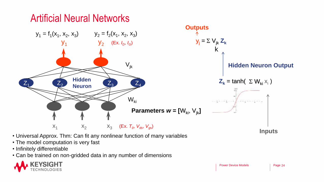
– Artificial neutral networks used for Q-V and I-V formulations
• Accurate fitting and infinitely differentiable
• Robust and fast model computation during simulation
– Self-heating and gate-lag/drain lag models included
• Dynamic behavior of GaN HEMT accurately captured
Power Device Models 22
𝑰𝑮 𝑰𝑫𝒅𝑸𝑮
𝒅𝒕
𝒅𝑸𝑫
𝒅𝒕
𝑮 𝑫
𝑺
𝑉𝑔𝑠
+
−
𝑉𝑑𝑠
+
−
DynaFET Core Model where 𝑰𝑮, 𝑰𝑫, 𝑸𝑮, and
𝑸𝑫 are Formulated Using ANNsJ. Xu, et al., “Dynamic FET Model – DynaFET - for GaN Transistors from NVNA Active Source Injection Measurements,” Proc. IEEE IMS, Tampa, FL, June, 2014

Page
Large-Signal NVNA Waveform Data Acquisition
Power Device Models 23
Synchronized
Bias Supplies Keysight E5270B
or 4142B
NVNA measurements performed at various:
(1) DC biases
(2) A11 power
(3) A21 power
(4) A21 phase
(5) Ambient temperatures
A11 power A21 power
A21 phasebias biasAmbient
temperatures
PA PABias
T
Bias
T
Controlled by an automated large-signal data
acquisition software application implemented
on top of the PNA-X NVNA
Time, nsec Time, nsec Time, nsec Time, nsec
J. Xu, et al., “Dynamic FET Model – DynaFET - for GaN Transistors from NVNA Active Source Injection Measurements,” Proc. IEEE IMS, Tampa, FL, June, 2014.
T.S. Nielsen, et al., “Doherty Power Amplifier Design in Gallium Nitride Technology Using a Nonlinear Vector Network Analyzer and X-Parameters,” Proc. IEEE CSICS, 2012.
Page
Artificial Neural Networks
Power Device Models 24
Z1 Z2 Z3 Z4
y1 y2
x1 x2 x3
Vjk
Wki
S Wki
Inputs
xi
Outputs
yj = S Vjk Zk
k
Parameters w = [Wki, Vjk]
• Universal Approx. Thm: Can fit any nonlinear function of many variables
• The model computation is very fast
• Infinitely differentiable
• Can be trained on non-gridded data in any number of dimensions
y1 = f1(x1, x2, x3)
Hidden Neuron Output
Zk = tanh( )
y2 = f2(x1, x2, x3)
Hidden
Neuron
(Ex. ID, IG)
(Ex. T0, Vds, Vgs)

Page
Gate-Lag/Drain-Lag Models
Power Device Models 25
*J. Xu, et al., “Large-signal FET Model with Multiple Time Scale Dynamics from Nonlinear Vector Network Analyzer Data,” IEEE MTT-S Int. MWS Digest, May, 2010, pp. 417-420.
capture
RF
emit
f
11
2 4 6 8 10 12 14 16 180 20
-8
-6
-4
-2
0
2
-10
4
time, nsec
ts(v
gsin
t[2
,::]-v
sin
t[2
,::])
ts(v
gsin
t_q
[2,::])
2 4 6 8 10 12 14 16 180 20
20
25
30
35
15
40
time, nsec
ts(v
dsin
t[2
,::]-v
sin
t[2
,::])
ts(v
dsin
t_q
[2,::])
2 4 6 8 10 12 14 16 180 20
-8
-6
-4
-2
0
2
-10
4
time, nsec
ts(v
gsin
t[1
,::]-v
sin
t[1
,::])
ts(v
gsin
t_q
[1,::])
2 4 6 8 10 12 14 16 180 20
20
25
30
35
15
40
time, nsec
ts(v
dsin
t[1
,::]-v
sin
t[1
,::])
ts(v
dsin
t_q
[1,::])
2 4 6 8 10 12 14 16 180 20
-8
-6
-4
-2
0
2
-10
4
time, nsec
ts(v
gsin
t[0
,::]-v
sin
t[0
,::])
ts(v
gsin
t_q
[0,::])
2 4 6 8 10 12 14 16 180 20
20
25
30
35
15
40
time, nsec
ts(v
dsin
t[0
,::]-v
sin
t[0
,::])
ts(v
dsin
t_q
[0,::])
(t))Min(V(t) gs1 (t))Max(V(t) ds2
(t)Vds
(t)2
(t)1
(t)Vgs

Page
DynaFET Model Extraction
Power Device Models 26
For model extraction
Auxiliary variables fixed at their steady-state large-signal values
In simulation
Auxiliary variables vary in time according to the coupled equivalent circuits
Auxiliary VariablesTerminal Voltages
(t))V(t), V(t), (t), (t), (t), T(t), V(VI(t)I dsgsjdsgsDdrain 21
NVNA
Waveforms
Auxiliary Variable
Generation
Constitutive Relation
Identification / Train Artificial Neural
Networks (ANNs)Terminal Voltages
(Vgs, Vds)
Natively Compiled
Model in ADS
Auxiliary
Variables
th0j RtV tITT )()(
))(())(( tVMax ,tVMin ds2gs1
(t))Ave(VV(t)) , Ave(VV dsdsgsgs
jT gsVdsV
21
(t))V(t), V(t), (t), (t), (t), T(t), V(VI(t)I dsgsjdsgsDdrain 21
dsgsjdsgs V V T VV 21
) , , , , , ,( 21 dsgsjdsgsD VVTVVI
ANNs used to model the detailed,
general, multi-variate coupling
• Accurate and general
• No additional assumptions
(e.g., backgating/virtual gate)

PageOutline
– Device models for silicon HV MOS transistors, silicon IGBTs,
SiC MOSFETs, and SiC IGBTs
– Device models for GaN HEMTs
– Summary
27Power Device Models

Page
Summary
– Design efficiency and time-to-market in power electronics requires advanced device models as
the industry keeps growing and becomes more competitive
• Better fitting accuracy
• Global coverage over operating conditions and simulation analyses
• Scalability over device geometry
• Support for electro-thermal simulation, etc.
– Power device modeling is actively researched for all types of material and device architectures.
– Industry standardization of GaN HEMT models is pursued through concerted effort by CMC
– DynaFET model provides a general, accurate modeling solution with excellent results for linear
and nonlinear simulation for GaN HEMTs enabled by NVNA data and ANN technology
Power Device Models 28

Page
Extra slides
Power Device Models 29

Page
Drain Lag in GaN HEMT
– Degradation of drain current caused by increase of the drain voltage of the quiescent
point, usually referred to as “current collapse” or “knee walkout”
Power Device Models 30
[-0.2, 4]
Vds (V)
Id (mA)
Pulsed I-V Measurements with Two Different Quiescent Points
[-0.8, 6]
“knee walkout”
Quiescent Bias PointId (mA)
Vds (V)

Page
Measurement Space
Copyright Keysight Technologies,
2014
31
Raytheon
6x60 mm
GaN HFET
Experiment design
covers entire
operating range;
Well beyond
static data
1-Tone, 16GHz
50ohm load
20V, 54mA
NVNA Measurements
DC
J. Xu, et al., “Dynamic FET Model – DynaFET - for GaN Transistors from NVNA Active Source Injection Measurements,” Proc. IEEE IMS, Tampa, FL, June, 2014.