Review of Charge Pump Topologies for Micro Energy ...thescipub.com/PDF/ajassp.2016.628.645.pdf ·...
18
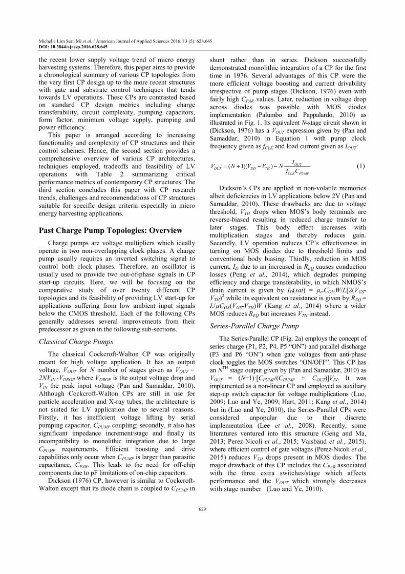
© 2016 Michelle Lim Sern Mi, Md. Shabiul Islam, Jahariah Sampe and Sawal Hamid Md. Ali. This open access article is distributed under a Creative Commons Attribution (CC-BY) 3.0 license. American Journal of Applied Sciences Review Articles Review of Charge Pump Topologies for Micro Energy Harvesting Systems 1,3 Michelle Lim Sern Mi, 1 Md. Shabiul Islam, 1 Jahariah Sampe and 2 Sawal Hamid Md. Ali 1 Institute of Microengineering and Nanoelectronics (IMEN), UKM, 43600 Bangi, Selangor, Malaysia 2 Department of Electrical, Electronics and System Engineering, UKM, 43600 Bangi, Selangor, Malaysia 3 Department of Physical Sciences, TARUC, Setapak, 53300 Kuala Lumpur, Malaysia Article history Received: 29-04-2016 Revised: 19-5-2016 Accepted: 25-05-2016 Corresponding Author: Michelle Lim Sern Mi Institute of Microengineering and Nanoelectronics (IMEN), UKM, 43600 Bangi, Selangor, Malaysia Email: [email protected] Abstract: This paper reviews CMOS based charge pump topologies used within autonomous embedded micro-systems. These charge pump structures have evolved from its simplistic diode-tied, single-branches with major threshold drops to exponential type, dual-branches with sophisticated gate and substrate control for lower voltage operation. Published charge pumps are grouped based on architecture, operation principles and pump optimization techniques with their pros and cons compared and results contrasted. The various charge pump topologies and schemes used are considered based on pumping efficiency, power efficiency, charge transferability, circuit complexity, pumping capacitors, form factor and minimum supply voltages with an optimum load. This article concludes with an overview of suitable techniques and recommendations that will aid a designer in selecting the most suitable charge pump topology especially for low ambient micro energy harvesting applications. Keywords: Charge Pump (CP), Low Voltage (LV), Energy Harvesting Introduction Next generation self-powered micro devices such as medical implants dictate the need for small, safe and renewable alternatives for battery replacement. Therefore, energy can be auton omously harvested from a patient without the need of future replacement such as the cochlear implant reported in (Bandyopadhyay, 2013). When scavenging these ambient energies, there is an inevitable discontinuity, typically mitigated by use of hybrid harvesters (Shi et al., 2011; Bandyopadhyay and Chandrakasan, 2012; Lim et al., 2013; Tan, 2013; Lim et al., 2014; Yeo et al., 2016). There is also a need to resolve the cold start issue for an inherently small (low voltage) harvester input. While off-the-shelf harvesters such as Photovoltaic (PV) cells (SANYO, 2008) and Piezoelectric (PZT) harvesters (MIDE, 2013) have voltages above the CMOS voltage threshold, V TH , Thermoelectric Generator (TEG) harvesters (CUI, 2012) generally fall in the mV range as low as 26 mV (Lim et al., 2014) at ∆T = 1K when CUI Peltier device is modelled upon. Therefore, efforts to kick-start CMOS based power management circuits for low voltage harvesters ranges from providing an external bias (Carlson et al., 2010; Kim and Kim, 2013; Ahmed and Mukhopadhyay, 2014), mechanical MEMs switch (Ramadass and Chandrakasan, 2010), charge pump based (Chen et al., 2011; Shih and Otis, 2011; Chen et al., 2012a; Liu et al., 2012; Bender et al., 2014; Peng et al., 2014), transformer based (Im et al., 2012; Teh and Mok, 2014; Zhang et al., 2014), oscillator based (Sun and Wu, 2010; Ahmed and Mukhopadhyay, 2014; Bender et al., 2014), one time wireless charging scheme (Bandyopadhyay, 2013) to a fully electrical multi-stage start-up mechanism (Chen et al., 2012b; Weng et al., 2013; Bender et al., 2014). Although these start-up scheme can push input voltage boundaries down to as low as 20 mV, they are either based on large inductors (Weng et al. , 2013) and transformers (Ahmed and Mukhopadhyay, 2014; Bender et al., 2014; Teh and Mok, 2014; Zhang et al., 2014) or off-chip components (Carlson et al., 2010; Ramadass and Chandrakasan, 2010; Kim and Kim, 2013) which limits how small the system can be. To overcome the aforementioned issues, only the Charge Pump (CP) topologies will be studied in this review due to its many benefits. These benefits include the possibility of full integration, lower form factor and its simplistic pumping mechanism. Previously published review article on CP circuits (Palumbo and Pappalardo, 2009) had a strong focus on design strategies and basic CP topologies. There were no mention of Low Voltage (LV) strategies and schemes for
Transcript of Review of Charge Pump Topologies for Micro Energy ...thescipub.com/PDF/ajassp.2016.628.645.pdf ·...
© 2016 Michelle Lim Sern Mi, Md. Shabiul Islam, Jahariah Sampe and Sawal Hamid Md. Ali. This open access article is
distributed under a Creative Commons Attribution (CC-BY) 3.0 license.
American Journal of Applied Sciences
Review Articles
Review of Charge Pump Topologies for Micro Energy
Harvesting Systems
1,3Michelle Lim Sern Mi,
1Md. Shabiul Islam,
1Jahariah Sampe and
2Sawal Hamid Md. Ali
1Institute of Microengineering and Nanoelectronics (IMEN), UKM, 43600 Bangi, Selangor, Malaysia 2Department of Electrical, Electronics and System Engineering, UKM, 43600 Bangi, Selangor, Malaysia 3Department of Physical Sciences, TARUC, Setapak, 53300 Kuala Lumpur, Malaysia
Article history
Received: 29-04-2016
Revised: 19-5-2016
Accepted: 25-05-2016
Corresponding Author:
Michelle Lim Sern Mi
Institute of Microengineering
and Nanoelectronics (IMEN),
UKM, 43600 Bangi, Selangor,
Malaysia Email: [email protected]
Abstract: This paper reviews CMOS based charge pump topologies used
within autonomous embedded micro-systems. These charge pump
structures have evolved from its simplistic diode-tied, single-branches with
major threshold drops to exponential type, dual-branches with sophisticated
gate and substrate control for lower voltage operation. Published charge
pumps are grouped based on architecture, operation principles and pump
optimization techniques with their pros and cons compared and results
contrasted. The various charge pump topologies and schemes used are
considered based on pumping efficiency, power efficiency, charge
transferability, circuit complexity, pumping capacitors, form factor and
minimum supply voltages with an optimum load. This article concludes
with an overview of suitable techniques and recommendations that will aid
a designer in selecting the most suitable charge pump topology especially
for low ambient micro energy harvesting applications.
Keywords: Charge Pump (CP), Low Voltage (LV), Energy Harvesting
Introduction
Next generation self-powered micro devices such
as medical implants dictate the need for small, safe
and renewable alternatives for battery replacement.
Therefore, energy can be auton omously harvested
from a patient without the need of future replacement
such as the cochlear implant reported in
(Bandyopadhyay, 2013). When scavenging these
ambient energies, there is an inevitable discontinuity,
typically mitigated by use of hybrid harvesters (Shi et
al., 2011; Bandyopadhyay and Chandrakasan, 2012;
Lim et al., 2013; Tan, 2013; Lim et al., 2014; Yeo et al.,
2016). There is also a need to resolve the cold start issue
for an inherently small (low voltage) harvester input.
While off-the-shelf harvesters such as Photovoltaic (PV)
cells (SANYO, 2008) and Piezoelectric (PZT) harvesters
(MIDE, 2013) have voltages above the CMOS voltage
threshold, VTH, Thermoelectric Generator (TEG)
harvesters (CUI, 2012) generally fall in the mV range as
low as 26 mV (Lim et al., 2014) at ∆T = 1K when CUI
Peltier device is modelled upon. Therefore, efforts to
kick-start CMOS based power management circuits for
low voltage harvesters ranges from providing an external
bias (Carlson et al., 2010; Kim and Kim, 2013; Ahmed and
Mukhopadhyay, 2014), mechanical MEMs switch
(Ramadass and Chandrakasan, 2010), charge pump based
(Chen et al., 2011; Shih and Otis, 2011; Chen et al.,
2012a; Liu et al., 2012; Bender et al., 2014; Peng et al.,
2014), transformer based (Im et al., 2012; Teh and Mok,
2014; Zhang et al., 2014), oscillator based (Sun and Wu,
2010; Ahmed and Mukhopadhyay, 2014; Bender et al.,
2014), one time wireless charging scheme
(Bandyopadhyay, 2013) to a fully electrical multi-stage
start-up mechanism (Chen et al., 2012b; Weng et al.,
2013; Bender et al., 2014). Although these start-up
scheme can push input voltage boundaries down to as
low as 20 mV, they are either based on large inductors
(Weng et al., 2013) and transformers (Ahmed and
Mukhopadhyay, 2014; Bender et al., 2014; Teh and
Mok, 2014; Zhang et al., 2014) or off-chip components
(Carlson et al., 2010; Ramadass and Chandrakasan,
2010; Kim and Kim, 2013) which limits how small the
system can be. To overcome the aforementioned issues,
only the Charge Pump (CP) topologies will be studied
in this review due to its many benefits. These benefits
include the possibility of full integration, lower form
factor and its simplistic pumping mechanism. Previously published review article on CP circuits
(Palumbo and Pappalardo, 2009) had a strong focus on design strategies and basic CP topologies. There were no mention of Low Voltage (LV) strategies and schemes for
Michelle Lim Sern Mi et al. / American Journal of Applied Sciences 2016, 13 (5): 628.645
DOI: 10.3844/ajassp.2016.628.645
629
the recent lower supply voltage trend of micro energy harvesting systems. Therefore, this paper aims to provide a chronological summary of various CP topologies from the very first CP design up to the more recent structures with gate and substrate control techniques that tends towards LV operations. These CPs are contrasted based on standard CP design metrics including charge transferability, circuit complexity, pumping capacitors, form factor, minimum voltage supply, pumping and power efficiency.
This paper is arranged according to increasing
functionality and complexity of CP structures and their
control schemes. Hence, the second section provides a
comprehensive overview of various CP architectures,
techniques employed, tradeoffs and feasibility of LV
operations with Table 2 summarizing critical
performance metrics of contemporary CP structures. The
third section concludes this paper with CP research
trends, challenges and recommendations of CP structures
suitable for specific design criteria especially in micro
energy harvesting applications.
Past Charge Pump Topologies: Overview
Charge pumps are voltage multipliers which ideally
operate in two non-overlapping clock phases. A charge
pump usually requires an inverted switching signal to
control both clock phases. Therefore, an oscillator is
usually used to provide two out-of-phase signals in CP
start-up circuits. Here, we will be focusing on the
comparative study of over twenty different CP
topologies and its feasibility of providing LV start-up for
applications suffering from low ambient input signals
below the CMOS threshold. Each of the following CPs
generally addresses several improvements from their
predecessor as given in the following sub-sections.
Classical Charge Pumps
The classical Cockcroft-Walton CP was originally
meant for high voltage application. It has an output
voltage, VOUT for N number of stages given as VOUT =
2NVIN -VDROP where VDROP is the output voltage drop and
VIN the peak input voltage (Pan and Samaddar, 2010).
Although Cockcroft-Walton CPs are still in use for
particle acceleration and X-ray tubes, the architecture is
not suited for LV application due to several reasons.
Firstly, it has inefficient voltage lifting by serial
pumping capacitor, CPUMP coupling; secondly, it also has
significant impedance increment/stage and finally its
incompatibility to monolithic integration due to large
CPUMP requirements. Efficient boosting and drive
capabilities only occur when CPUMP is larger than parasitic
capacitance, CPAR. This leads to the need for off-chip
components due to pF limitations of on-chip capacitors.
Dickson (1976) CP, however is similar to Cockcroft-
Walton except that its diode chain is coupled to CPUMP in
shunt rather than in series. Dickson successfully
demonstrated monolithic integration of a CP for the first
time in 1976. Several advantages of this CP were the
more efficient voltage boosting and current drivability
irrespective of pump stages (Dickson, 1976) even with
fairly high CPAR values. Later, reduction in voltage drop
across diodes was possible with MOS diodes
implementation (Palumbo and Pappalardo, 2010) as
illustrated in Fig. 1. Its equivalent N-stage circuit shown in
(Dickson, 1976) has a VOUT expression given by (Pan and
Samaddar, 2010) in Equation 1 with pump clock
frequency given as fCLK and load current given as IOUT:
( 1)( ) OUTOUT DD TH
CLK PUMP
IV N V V N
f C= + − − (1)
Dickson’s CPs are applied in non-volatile memories
albeit deficiencies in LV applications below 2V (Pan and
Samaddar, 2010). These drawbacks are due to voltage
threshold, VTH drops when MOS’s body terminals are
reverse-biased resulting in reduced charge transfer to
later stages. This body effect increases with
multiplication stages and thereby reduces gain.
Secondly, LV operation reduces CP’s effectiveness in
turning on MOS diodes due to threshold limits and
conventional body biasing. Thirdly, reduction in MOS
current, ID due to an increased in REQ causes conduction
losses (Peng et al., 2014), which degrades pumping
efficiency and charge transferability, in which NMOS’s
drain current is given by ID(sat) = µn·COX·W/L[2(VGS-
VTH)2 while its equivalent on resistance is given by REQ =
L/µCOX(VGS-VTH)W (Kang et al., 2014) where a wider
MOS reduces REQ but increases VTH instead.
Series-Parallel Charge Pump
The Series-Parallel CP (Fig. 2a) employs the concept of
series charge (P1, P2, P4, P5 “ON”) and parallel discharge
(P3 and P6 “ON”) when gate voltages from anti-phase
clock toggles the MOS switches “ON/OFF”. This CP has
an NTH
stage output given by (Pan and Samaddar, 2010) as
VOUT = (N+1)·[CPUMP/(CPUMP + COUT)]VIN. It was
implemented as a non-linear CP and employed as auxiliary
step-up switch capacitor for voltage multiplications (Luo,
2009; Luo and Ye, 2009; Hart, 2011; Kang et al., 2014)
but in (Luo and Ye, 2010), the Series-Parallel CPs were
considered unpopular due to their discrete
implementation (Lee et al., 2008). Recently, some
literatures ventured into this structure (Geng and Ma,
2013; Perez-Nicoli et al., 2015; Vaisband et al., 2015),
where efficient control of gate voltages (Perez-Nicoli et al.,
2015) reduces VTH drops present in MOS diodes. The
major drawback of this CP includes the CPAR associated
with the three extra switches/stage which affects
performance and the VOUT which strongly decreases
with stage number (Luo and Ye, 2010).
Michelle Lim Sern Mi et al. / American Journal of Applied Sciences 2016, 13 (5): 628.645
DOI: 10.3844/ajassp.2016.628.645
630
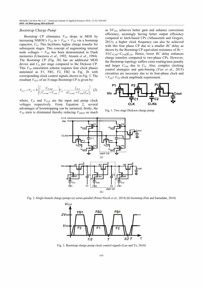
Bootstrap Charge Pump
Bootstrap CP eliminates VTH drops in MOS by
increasing NMOS’s VGS to > VDD + VTH via a bootstrap
capacitor, Cbt. This facilitates higher charge transfer for
subsequent stages. This concept of augmenting internal
node voltages > VDD has been demonstrated in Flash
memories (Umezawa et al., 1992; Atsumi et al., 1994).
The Bootstrap CP (Fig. 2b) has an additional MOS
device and Cbt per stage compared to the Dickson CP.
This VTH cancelation scheme requires four clock phases
annotated as F1, FB1, F2, FB2 in Fig. 2b with
corresponding clock control signals shown in Fig. 3. The
resultant VOUT of an N-stage Bootstrap CP is given by:
( )
PUMP OUTOUT IN clk
PUMP PAR PUMP PAR clk
C IV V N V
C C C C f
= + −
+ + (2)
where, VIN and VCLK are the input and pump clock
voltages respectively. From Equation 2, several
advantages of bootstrapping can be surmised, firstly, the
VTH term is eliminated thereby reducing VDROP as much
as NVTH, achieves better gain and enhance conversion
efficiency, seemingly having better output efficiency
compared to latch-based CPs (Allasasmeh and Gregori,
2011), a higher clock frequency can also be achieved
with this four phase CP due to a smaller RC delay as
shown by the Bootstrap CP equivalent resistance of Rs =
N/(CPUMP+CPAR)fCLK. Hence, lower RC delay enhances
charge transfers compared to two-phase CPs. However,
the Bootstrap topology suffers extra routing/area penalty
and larger CPAR due to Cbt. Also, complex clocking
control strategies and gate-biasing (Yeo et al., 2015)
circuitries are necessary due to its four-phase clock and
>VDD+VTH clock amplitude requirement.
Fig. 1. Two stage Dickson charge pump
(a)
(b)
Fig. 2. Single branch charge pumps (a) series-parallel (Perez-Nicoli et al., 2014) (b) bootstrap (Pan and Samaddar, 2010)
Fig. 3. Bootstrap charge pump clock control signals (Luo and Ye, 2010)
Michelle Lim Sern Mi et al. / American Journal of Applied Sciences 2016, 13 (5): 628.645
DOI: 10.3844/ajassp.2016.628.645
631
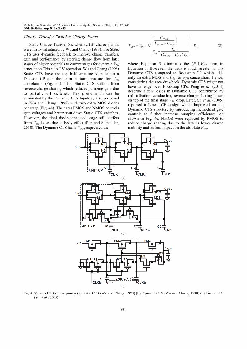
Charge Transfer Switches Charge Pump
Static Charge Transfer Switches (CTS) charge pumps
were firstly introduced by Wu and Chang (1998). The Static
CTS uses dynamic feedback to improve charge transfers,
gain and performance by steering charge flow from later
stages of higher potentials to current stages for dynamic VTH
cancelation This suits LV operation. Wu and Chang (1998)
Static CTS have the top half structure identical to a
Dickson CP and the extra bottom structure for VTH
cancelation (Fig. 4a). This Static CTS suffers from
reverse charge sharing which reduces pumping gain due
to partially off switches. This phenomenon can be
eliminated by the Dynamic CTS topology also proposed
in (Wu and Chang, 1998) with two extra MOS diodes
per stage (Fig. 4b). The extra PMOS and NMOS controls
gate voltages and better shut down Static CTS switches.
However, the final diode-connected stage still suffers
from VTH losses due to body effect (Pan and Samaddar,
2010). The Dynamic CTS has a VOUT expressed as:
( )
PUMP
PUMP PAR
OUT IN TH
OUTclk
PUMP PAR clk
C
C CV V N V
IV
C C f
+ = + − −
+
(3)
where Equation 3 eliminates the (N-1)VTH term in Equation 1. However, the CPAR is much greater in this Dynamic CTS compared to Bootstrap CP which adds only an extra MOS and Cbt for VTH cancelation. Hence, considering the area drawback, Dynamic CTS might not have an edge over Bootstrap CPs. Peng et al. (2014) describe a few losses in Dynamic CTS contributed by redistribution, conduction, reverse charge sharing losses on top of the final stage VTH drop. Later, Su et al. (2005) reported a Linear CP design which improved on the Dynamic CTS structure by introducing methodical gate controls to further increase pumping efficiency. As shown in Fig. 4c, NMOS were replaced by PMOS to reduce charge sharing due to the latter’s lower charge mobility and its less impact on the absolute VTH.
(a)
(b)
(c)
Fig. 4. Various CTS charge pumps (a) Static CTS (Wu and Chang, 1998) (b) Dynamic CTS (Wu and Chang, 1998) (c) Linear CTS
(Su et al., 2005)
Michelle Lim Sern Mi et al. / American Journal of Applied Sciences 2016, 13 (5): 628.645
DOI: 10.3844/ajassp.2016.628.645
632
(a)
(b)
Fig. 5. Basic dual-branch charge pumps (Palumbo and Pappalardo, 2010) (a) two branch Dickson (b) two branch bootstrap
Therefore, widening PMOS reduces conduction loss
(Maksimovic and Dhar, 1999) by lowering REQ. There is
also an efficient turn-on of last stage by disregarding the
use of MOS diodes as in (Wu and Chang, 1998).
However, if VDD <VTH, the Linear CP yet again cannot
turn on/off the switches effectively.
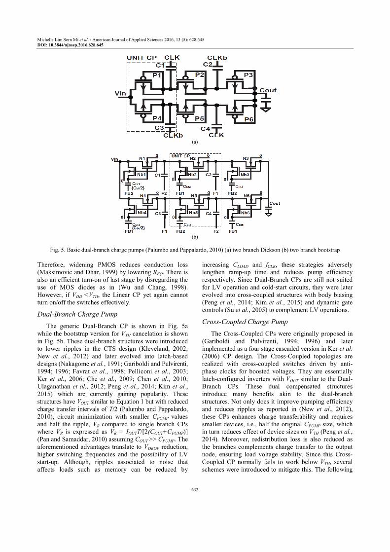
Dual-Branch Charge Pump
The generic Dual-Branch CP is shown in Fig. 5a
while the bootstrap version for VTH cancelation is shown
in Fig. 5b. These dual-branch structures were introduced
to lower ripples in the CTS design (Kleveland, 2002;
New et al., 2012) and later evolved into latch-based
designs (Nakagome et al., 1991; Gariboldi and Pulvirenti,
1994; 1996; Favrat et al., 1998; Pelliconi et al., 2003;
Ker et al., 2006; Che et al., 2009; Chen et al., 2010;
Ulaganathan et al., 2012; Peng et al., 2014; Kim et al.,
2015) which are currently gaining popularity. These
structures have VOUT similar to Equation 1 but with reduced
charge transfer intervals of T/2 (Palumbo and Pappalardo,
2010), circuit minimization with smaller CPUMP values
and half the ripple, VR compared to single branch CPs
where VR is expressed as VR = IOUTT/[2(COUT+CPUMP)]
(Pan and Samaddar, 2010) assuming COUT >> CPUMP. The
aforementioned advantages translate to VDROP reduction,
higher switching frequencies and the possibility of LV
start-up. Although, ripples associated to noise that
affects loads such as memory can be reduced by
increasing CLOAD and fCLK, these strategies adversely
lengthen ramp-up time and reduces pump efficiency
respectively. Since Dual-Branch CPs are still not suited
for LV operation and cold-start circuits, they were later
evolved into cross-coupled structures with body biasing
(Peng et al., 2014; Kim et al., 2015) and dynamic gate
controls (Su et al., 2005) to complement LV operations.
Cross-Coupled Charge Pump
The Cross-Coupled CPs were originally proposed in
(Gariboldi and Pulvirenti, 1994; 1996) and later
implemented as a four stage cascaded version in Ker et al.
(2006) CP design. The Cross-Coupled topologies are
realized with cross-coupled switches driven by anti-
phase clocks for boosted voltages. They are essentially
latch-configured inverters with VOUT similar to the Dual-
Branch CPs. These dual compensated structures
introduce many benefits akin to the dual-branch
structures. Not only does it improve pumping efficiency
and reduces ripples as reported in (New et al., 2012),
these CPs enhances charge transferability and requires
smaller devices, i.e., half the original CPUMP size, which
in turn reduces effect of device sizes on VTH (Peng et al.,
2014). Moreover, redistribution loss is also reduced as
the branches complements charge transfer to the output
node, ensuring load voltage stability. Since this Cross-
Coupled CP normally fails to work below VTH, several
schemes were introduced to mitigate this. The following
Michelle Lim Sern Mi et al. / American Journal of Applied Sciences 2016, 13 (5): 628.645
DOI: 10.3844/ajassp.2016.628.645
633
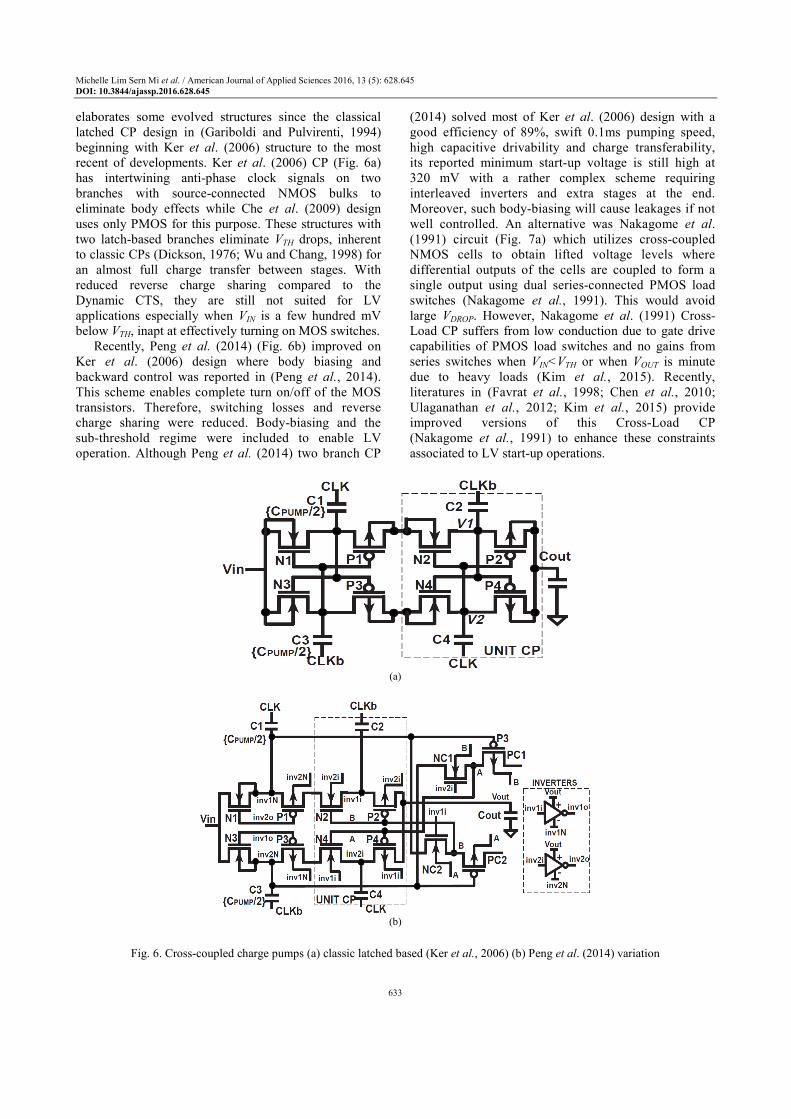
elaborates some evolved structures since the classical
latched CP design in (Gariboldi and Pulvirenti, 1994)
beginning with Ker et al. (2006) structure to the most
recent of developments. Ker et al. (2006) CP (Fig. 6a)
has intertwining anti-phase clock signals on two
branches with source-connected NMOS bulks to
eliminate body effects while Che et al. (2009) design
uses only PMOS for this purpose. These structures with
two latch-based branches eliminate VTH drops, inherent
to classic CPs (Dickson, 1976; Wu and Chang, 1998) for
an almost full charge transfer between stages. With
reduced reverse charge sharing compared to the
Dynamic CTS, they are still not suited for LV
applications especially when VIN is a few hundred mV
below VTH, inapt at effectively turning on MOS switches.
Recently, Peng et al. (2014) (Fig. 6b) improved on
Ker et al. (2006) design where body biasing and
backward control was reported in (Peng et al., 2014).
This scheme enables complete turn on/off of the MOS
transistors. Therefore, switching losses and reverse
charge sharing were reduced. Body-biasing and the
sub-threshold regime were included to enable LV
operation. Although Peng et al. (2014) two branch CP
(2014) solved most of Ker et al. (2006) design with a
good efficiency of 89%, swift 0.1ms pumping speed,
high capacitive drivability and charge transferability,
its reported minimum start-up voltage is still high at
320 mV with a rather complex scheme requiring
interleaved inverters and extra stages at the end.
Moreover, such body-biasing will cause leakages if not
well controlled. An alternative was Nakagome et al.
(1991) circuit (Fig. 7a) which utilizes cross-coupled
NMOS cells to obtain lifted voltage levels where
differential outputs of the cells are coupled to form a
single output using dual series-connected PMOS load
switches (Nakagome et al., 1991). This would avoid
large VDROP. However, Nakagome et al. (1991) Cross-
Load CP suffers from low conduction due to gate drive
capabilities of PMOS load switches and no gains from
series switches when VIN<VTH or when VOUT is minute
due to heavy loads (Kim et al., 2015). Recently,
literatures in (Favrat et al., 1998; Chen et al., 2010;
Ulaganathan et al., 2012; Kim et al., 2015) provide
improved versions of this Cross-Load CP
(Nakagome et al., 1991) to enhance these constraints
associated to LV start-up operations.
(a)
(b)
Fig. 6. Cross-coupled charge pumps (a) classic latched based (Ker et al., 2006) (b) Peng et al. (2014) variation
Michelle Lim Sern Mi et al. / American Journal of Applied Sciences 2016, 13 (5): 628.645
DOI: 10.3844/ajassp.2016.628.645
634
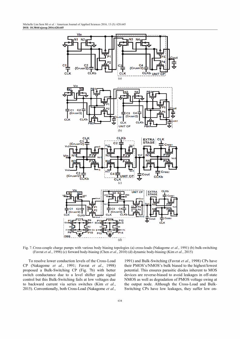
(a)
(b)
(c)
(d)
Fig. 7. Cross-couple charge pumps with various body biasing topologies (a) cross-loads (Nakagome et al., 1991) (b) bulk-switching
(Favrat et al., 1998) (c) forward body-biasing (Chen et al., 2010) (d) dynamic body-biasing (Kim et al., 2015)
To resolve lower conduction levels of the Cross-Load
CP (Nakagome et al., 1991; Favrat et al., 1998)
proposed a Bulk-Switching CP (Fig. 7b) with better
switch conductance due to a level shifter gate signal
control but this Bulk-Switching fails at low voltages due
to backward current via series switches (Kim et al.,
2015). Conventionally, both Cross-Load (Nakagome et al.,
1991) and Bulk-Switching (Favrat et al., 1998) CPs have
their PMOS’s/NMOS’s bulk biased to the highest/lowest
potential. This ensures parasitic diodes inherent to MOS
devices are reverse-biased to avoid leakages in off-state
NMOS as well as degradation of PMOS voltage swing at
the output node. Although the Cross-Load and Bulk-
Switching CPs have low leakages, they suffer low on-
Michelle Lim Sern Mi et al. / American Journal of Applied Sciences 2016, 13 (5): 628.645
DOI: 10.3844/ajassp.2016.628.645
635
current, ION. The low gain in Cross-Load CP is also
unresolved in the Bulk-Switching CP due to weakly off
switches. Hence, increasing (decreasing) NMOS’s
(PMOS) body bias reduces VTH to facilitate lower turn-
on voltages such as the Forward-Body-Bias (FBB) CP
proposed by (Chen et al., 2010; Peng et al., 2014).
The FBB CP uses higher inter-stage voltages
borrowed from future stages to reduce VTH of NMOS
while PMOS is biased to the lowest ground potential
(Fig. 7c). Thus, all MOS devices are forward biased at
all times during both “ON” and “OFF” states. This leads
to both high current transfer and high body leakages
when MOS devices are not conducting. This increases
Voltage Conversion Efficiency (VCE) but reduces
Power Conversion Efficiency (PCE). To resolve this
issue, the Dynamic-Body-Biasing (DBB) CP was
proposed by Kim et al. (2015) recently (Fig. 7d) with
consideration of dead-time limitations, conduction loss
and Meindl limit (Meindl and Davis, 2000). The DBB
CP maintains a high on current during “ON” states and
at the same time reduce leakages during “OFF” states by
dynamically switching MOS devices into low VTH
(forward-biased) and high VTH (reverse-biased) devices
on demand, widely known as the Variable Threshold
CMOS technique (VTCMOS) (Kang et al., 2014). The
low VTH enables LV operation and faster speed whereas
higher VTH reduces sub-threshold leakages and enhances
efficiency. While the DBB CP in (Kim et al., 2015) have
benefits such as low processing cost, low start-up
voltages at 150 mV, high efficiency of 72.5% at VIN =
450 mV and reduced leakages while maintaining high on
current which promotes LV applications, the structure
suffers from additional DBB control circuitry, usages of
6×10 nF off-chip capacitors and still a low 34% pumping
efficiency at low voltages (180 mV). On the other hand,
Bandyopadhyay et al. (2014) proposed an ultra low
power CP similar to Fig. 7b with a gate driver that
reduces leakages based on Favrat et al. (1998) voltage
doublers model.
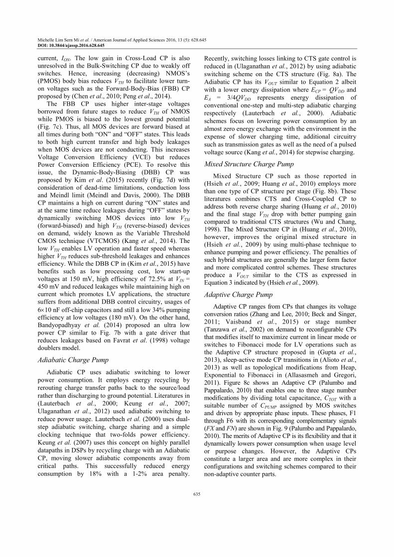
Adiabatic Charge Pump
Adiabatic CP uses adiabatic switching to lower
power consumption. It employs energy recycling by
rerouting charge transfer paths back to the source/load
rather than discharging to ground potential. Literatures in
(Lauterbach et al., 2000; Keung et al., 2007;
Ulaganathan et al., 2012) used adiabatic switching to
reduce power usage. Lauterbach et al. (2000) uses dual-
step adiabatic switching, charge sharing and a simple
clocking technique that two-folds power efficiency.
Keung et al. (2007) uses this concept on highly parallel
datapaths in DSPs by recycling charge with an Adiabatic
CP, moving slower adiabatic components away from
critical paths. This successfully reduced energy
consumption by 18% with a 1-2% area penalty.
Recently, switching losses linking to CTS gate control is
reduced in (Ulaganathan et al., 2012) by using adiabatic
switching scheme on the CTS structure (Fig. 8a). The
Adiabatic CP has its VOUT similar to Equation 2 albeit
with a lower energy dissipation where ECP = QVDD and
EA = 3/4QVDD represents energy dissipation of
conventional one-step and multi-step adiabatic charging
respectively (Lauterbach et al., 2000). Adiabatic
schemes focus on lowering power consumption by an
almost zero energy exchange with the environment in the
expense of slower charging time, additional circuitry
such as transmission gates as well as the need of a pulsed
voltage source (Kang et al., 2014) for stepwise charging.
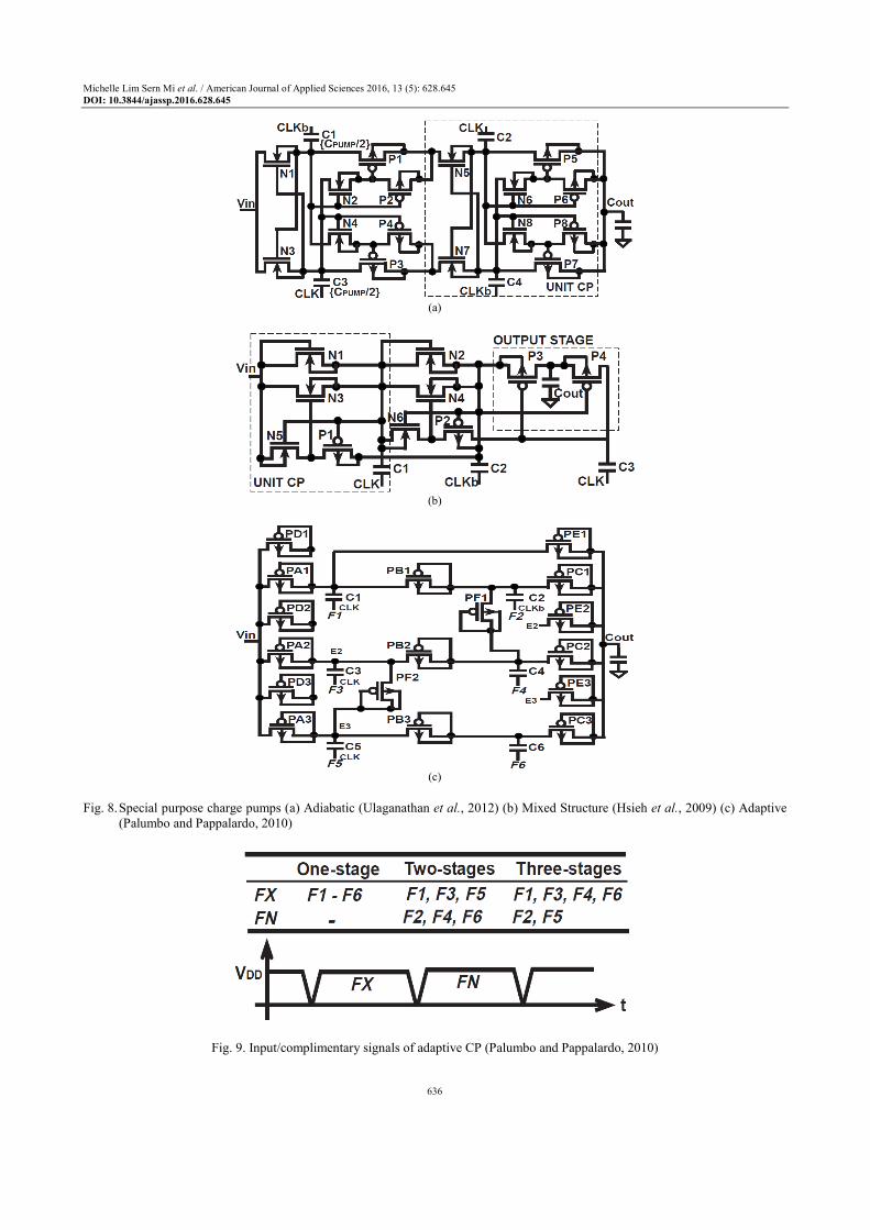
Mixed Structure Charge Pump
Mixed Structure CP such as those reported in
(Hsieh et al., 2009; Huang et al., 2010) employs more
than one type of CP structure per stage (Fig. 8b). These
literatures combines CTS and Cross-Coupled CP to
address both reverse charge sharing (Huang et al., 2010)
and the final stage VTH drop with better pumping gain
compared to traditional CTS structures (Wu and Chang,
1998). The Mixed Structure CP in (Huang et al., 2010),
however, improves the original mixed structure in
(Hsieh et al., 2009) by using multi-phase technique to
enhance pumping and power efficiency. The penalties of
such hybrid structures are generally the larger form factor
and more complicated control schemes. These structures
produce a VOUT similar to the CTS as expressed in
Equation 3 indicated by (Hsieh et al., 2009).
Adaptive Charge Pump
Adaptive CP ranges from CPs that changes its voltage
conversion ratios (Zhang and Lee, 2010; Beck and Singer,
2011; Vaisband et al., 2015) or stage number
(Tanzawa et al., 2002) on demand to reconfigurable CPs
that modifies itself to maximize current in linear mode or
switches to Fibonacci mode for LV operations such as
the Adaptive CP structure proposed in (Gupta et al.,
2013), sleep-active mode CP transitions in (Alioto et al.,
2013) as well as topological modifications from Heap,
Exponential to Fibonacci in (Allasasmeh and Gregori,
2011). Figure 8c shows an Adaptive CP (Palumbo and
Pappalardo, 2010) that enables one to three stage number
modifications by dividing total capacitance, CTOT with a
suitable number of CPUMP assigned by MOS switches
and driven by appropriate phase inputs. These phases, F1
through F6 with its corresponding complementary signals
(FX and FN) are shown in Fig. 9 (Palumbo and Pappalardo,
2010). The merits of Adaptive CP is its flexibility and that it
dynamically lowers power consumption when usage level
or purpose changes. However, the Adaptive CPs
constitute a larger area and are more complex in their
configurations and switching schemes compared to their
non-adaptive counter parts.
Michelle Lim Sern Mi et al. / American Journal of Applied Sciences 2016, 13 (5): 628.645
DOI: 10.3844/ajassp.2016.628.645
636
(a)
(b)
(c)
Fig. 8. Special purpose charge pumps (a) Adiabatic (Ulaganathan et al., 2012) (b) Mixed Structure (Hsieh et al., 2009) (c) Adaptive
(Palumbo and Pappalardo, 2010)
Fig. 9. Input/complimentary signals of adaptive CP (Palumbo and Pappalardo, 2010)
Michelle Lim Sern Mi et al. / American Journal of Applied Sciences 2016, 13 (5): 628.645
DOI: 10.3844/ajassp.2016.628.645
637
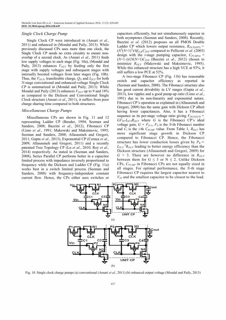
Single Clock Charge Pump
Single Clock CP were introduced in (Ansari et al., 2011) and enhanced in (Mondal and Paily, 2013). While previously discussed CPs uses more than one clock, the Single Clock CP needs no extra circuitry to ensure non-overlap of a second clock. As (Ansari et al., 2011) feeds low supply voltages to each stage (Fig. 10a), (Mondal and Paily, 2013) enhances VOUT by feeding only the first stage with supply voltages and subsequent stages with internally boosted voltages from later stages (Fig. 10b). Thus, the VOUT, transferable charge, QN and IOUT for both N-stage conventional and enhanced-voltage Single Clock CP is summarized in (Mondal and Paily, 2013). While Mondal and Paily (2013) enhances VOUT up to 9 and 18% as compared to the Dickson and Conventional Single Clock structure (Ansari et al., 2011), it suffers from poor charge sharing time compared to both structures.
Miscellaneous Charge Pumps
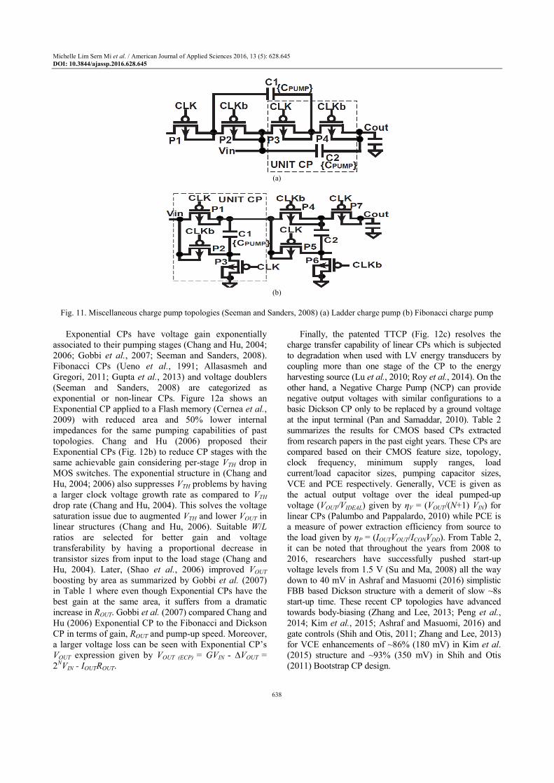
Miscellaneous CPs are shown in Fig. 11 and 12 representing Ladder CP (Bender, 1994; Seeman and Sanders, 2008; Bazzini et al., 2012), Fibonacci CP (Ueno et al., 1991; Makowski and Maksimovic, 1995; Seeman and Sanders, 2008; Allasasmeh and Gregori,
2011; Gupta et al., 2013), Exponential CP (Cernea et al., 2009; Allasasmeh and Gregori, 2011) and a recently patented Tree Topology CP (Lu et al., 2010; Roy et al., 2014) respectively. As stated in (Seeman and Sanders, 2008), Series Parallel CP performs better in a capacitor limited process with impedance inversely proportional to
frequency while the Dickson and Ladder CP (Fig. 11a) works best in a switch limited process (Seeman and Sanders, 2008) with frequency-independent constant current flow. Hence, the CPs either uses switches or
capacitors efficiently, but not simultaneously superior in both asymptotes (Seeman and Sanders, 2008). Recently, Bazzini et al. (2012) proposes an all PMOS Double Ladder CP which lowers output resistance, ROUT(OPT) =
(N2(N+1)
2)/4fCLKCTOT compared to Pelliconi et al. (2003)
design with the i-stage pumping capacitor, CPUMP(i) = (N+1-i)/(N(N+1)CTOT (Bazzini et al., 2012) chosen to minimize ROUT (Makowski and Maksimovic, 1995). While this enhanced structure has a high VCE at 93%, it still suffers a low PCE at 52%.
A two-stage Fibonacci CP (Fig. 11b) has reasonable
switch and capacitor efficiency as reported in
(Seeman and Sanders, 2008). The Fibonacci structure also
has good current drivability in LV ranges (Gupta et al.,
2013), low ripples and a good pump-up ratio (Ueno et al.,
1991) due to its non-linearity and exponential nature.
Fibonacci CP’s operation as explained in (Allasasmeh and
Gregori, 2009) has the same gain with Dickson CP albeit
having fewer capacitances. Also, it has a Fibonacci
sequence as its per-stage voltage ratio giving VOUT(FCP) =
GVIN-IOUTROUT where G is the Fibonacci CP’s ideal
voltage gain, G = FN+1, FN is the N-th Fibonacci number
and Ci is the i-th CPUMP value. From Table 1, ROUT has
more significant stage growth in Dickson CP
compared to Fibonacci CP. Hence, the Fibonacci
structure has lower conduction losses given by PR =
IOUT 2ROUT leading to better energy efficiency than the
Dickson structure (Allasasmeh and Gregori, 2009) for
G > 3. There are however no difference in ROUT
between them for G ≤ 3 or N ≤ 2. Unlike Dickson
CPs, CPUMP in Fibonacci CPs are not equally sized in
all stages. For optimal performance, the N-th stage
Fibonacci CP requires the largest capacitor nearest to
VIN and the smallest capacitor to be closest to the load.
(a)
(b)
Fig. 10. Single clock charge pumps (a) conventional (Ansari et al., 2011) (b) enhanced output voltage (Mondal and Paily, 2013)
Michelle Lim Sern Mi et al. / American Journal of Applied Sciences 2016, 13 (5): 628.645
DOI: 10.3844/ajassp.2016.628.645
638
(a)
(b)
Fig. 11. Miscellaneous charge pump topologies (Seeman and Sanders, 2008) (a) Ladder charge pump (b) Fibonacci charge pump
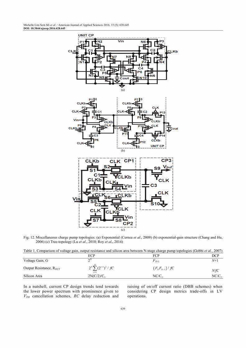
Exponential CPs have voltage gain exponentially
associated to their pumping stages (Chang and Hu, 2004;
2006; Gobbi et al., 2007; Seeman and Sanders, 2008).
Fibonacci CPs (Ueno et al., 1991; Allasasmeh and
Gregori, 2011; Gupta et al., 2013) and voltage doublers
(Seeman and Sanders, 2008) are categorized as
exponential or non-linear CPs. Figure 12a shows an
Exponential CP applied to a Flash memory (Cernea et al.,
2009) with reduced area and 50% lower internal
impedances for the same pumping capabilities of past
topologies. Chang and Hu (2006) proposed their
Exponential CPs (Fig. 12b) to reduce CP stages with the
same achievable gain considering per-stage VTH drop in
MOS switches. The exponential structure in (Chang and
Hu, 2004; 2006) also suppresses VTH problems by having
a larger clock voltage growth rate as compared to VTH
drop rate (Chang and Hu, 2004). This solves the voltage
saturation issue due to augmented VTH and lower VOUT in
linear structures (Chang and Hu, 2006). Suitable W/L
ratios are selected for better gain and voltage
transferability by having a proportional decrease in
transistor sizes from input to the load stage (Chang and
Hu, 2004). Later, (Shao et al., 2006) improved VOUT
boosting by area as summarized by Gobbi et al. (2007)
in Table 1 where even though Exponential CPs have the
best gain at the same area, it suffers from a dramatic
increase in ROUT. Gobbi et al. (2007) compared Chang and
Hu (2006) Exponential CP to the Fibonacci and Dickson
CP in terms of gain, ROUT and pump-up speed. Moreover,
a larger voltage loss can be seen with Exponential CP’s
VOUT expression given by VOUT (ECP) = GVIN - ∆VOUT =
2NVIN - IOUTROUT.
Finally, the patented TTCP (Fig. 12c) resolves the
charge transfer capability of linear CPs which is subjected
to degradation when used with LV energy transducers by
coupling more than one stage of the CP to the energy
harvesting source (Lu et al., 2010; Roy et al., 2014). On the
other hand, a Negative Charge Pump (NCP) can provide
negative output voltages with similar configurations to a
basic Dickson CP only to be replaced by a ground voltage
at the input terminal (Pan and Samaddar, 2010). Table 2
summarizes the results for CMOS based CPs extracted
from research papers in the past eight years. These CPs are
compared based on their CMOS feature size, topology,
clock frequency, minimum supply ranges, load
current/load capacitor sizes, pumping capacitor sizes,
VCE and PCE respectively. Generally, VCE is given as
the actual output voltage over the ideal pumped-up
voltage (VOUT/VIDEAL) given by ηV = (VOUT/(N+1) VIN) for
linear CPs (Palumbo and Pappalardo, 2010) while PCE is
a measure of power extraction efficiency from source to
the load given by ηP = (IOUTVOUT/ICONVDD). From Table 2,
it can be noted that throughout the years from 2008 to
2016, researchers have successfully pushed start-up
voltage levels from 1.5 V (Su and Ma, 2008) all the way
down to 40 mV in Ashraf and Masuomi (2016) simplistic
FBB based Dickson structure with a demerit of slow ~8s
start-up time. These recent CP topologies have advanced
towards body-biasing (Zhang and Lee, 2013; Peng et al.,
2014; Kim et al., 2015; Ashraf and Masuomi, 2016) and
gate controls (Shih and Otis, 2011; Zhang and Lee, 2013)
for VCE enhancements of ~86% (180 mV) in Kim et al.
(2015) structure and ~93% (350 mV) in Shih and Otis
(2011) Bootstrap CP design.
Michelle Lim Sern Mi et al. / American Journal of Applied Sciences 2016, 13 (5): 628.645
DOI: 10.3844/ajassp.2016.628.645
639
(a)
(b)
(c)
Fig. 12. Miscellaneous charge pump topologies: (a) Exponential (Cernea et al., 2009) (b) exponential-gain structure (Chang and Hu,
2006) (c) Tree-topology (Lu et al., 2010; Roy et al., 2014)
Table 1. Comparison of voltage gain, output resistance and silicon area between N-stage charge pump topologies (Gobbi et al., 2007)
ECP FCP DCP
Voltage Gain, G 2N FN+1 N+1
Output Resistance, ROUT 1 2
1
2 (2 ) /N
N i
i
fC−
=∑ ( )1 /N NF F fC− N/fC
Silicon Area 2N(C/2)/C NC/C NC/C
In a nutshell, current CP design trends tend towards
the lower power spectrum with prominence given to
VTH cancellation schemes, RC delay reduction and
raising of on/off current ratio (DBB schemes) when
considering CP design metrics trade-offs in LV
operations.
Michelle Lim Sern Mi et al. / American Journal of Applied Sciences 2016, 13 (5): 628.645
DOI: 10.3844/ajassp.2016.628.645
640
Table 2. Contemporary charge pump topologies: A performance comparison
Parameters
---------------------------------------------------------------------------------------------------------------------------------------------------------------------------------------------
CP Topology Minimum Clock Pumping Load/ Load VCE Process
Authors (Year) (No. of stages/ supply, Frequency, Capacitors, Capacitor, (PCE) technology
Branches) VIN fCLK CPUMP IOUT/ CLOAD (CMOS) Advantages Disadvantages
Ashraf and Dickson with 40 mV 1 kHz N/A CLOAD = 5 nF 53.88%@40 mV 180-nm Lowest VIN Slow pre-startup at ~8s
Masoumi (2016) FBB (CP output) (N/A) Simplistic FBB Large no. of MOSFETs
(5×20-stages/1) approach
Kim et al. (2015) Cross-coupled 150 mV 250 kHz 10 nF ×6 IOUT = 21 uA 85.97% @ 0.18V 130-nm Low VIN Off-chip capacitors
with DBB (off-chip) @ VIN = 0.18V (34% @ 0.18V) Highest IOUT Extra complexity for
(3-stages/2) [VOUT = 0.5 V] (72.5% @0.45V) High Efficiency clocking & dynamic
Balances good bulk-biasing
PCE and VCE
Peng et al. (2014) Cross-coupled 320 mV 450 kHz 24pF ×12 CLOAD = 50.7 pF 89% @ 0.32V 180-nm Swift pumping Rather complex scheme
body- biased & (on-chip) (N/A) rate at 0.1 ms requiring interleaved
backward control Good VCE inverters and extra
(6-stages/2) Reduce leakages stages at the end
with body-biasing
for PMOS only
Zhang and Lee. (2013) Dickson based 900 mV 7 MHz 20 pF ×4 CLOAD = 40 pF 84%@0.90V 350-nm No VTH drop High VIN
gain-enhanced (on-chip) RLOAD = 300 Ω 84.62%@1.4V No body-effect
dynamic gate & IOUT = 76uA (43% @1.4V) No floating substrate
substrate control @ VIN = 1.4V terminals/ lower RON
(4-stages/ 1) [VOUT = 4.5V]
Chen et al. (2012a) Dickson based 120 mV 1 MHz, 28.6 pF ×20 IOUT = 7uA 58.33% @ 0.12V 65-nm High PCE Low IOUT
dual mode (startup) (on-chip) @ VIN = 0.18V (38.8% @ 0.12V) Low VIN High process cost
[startup/ 20 MHz (extrapolation) No external
operation mode] (operation) [VOUT = 0.5 V] excitation
(10-stages/1)
Shih and Otis (2011) Bootstrap 270 mV 800 kHz 25 pF ×6 CLOAD = 500pF 92.86% @ 0.35V 130-nm Fully integrated Requires 4 clock
(3-stages/ 1) (on-chip) IOUT = 5uA (56% @ 0.45V) Low process cost phases
@ VIN = 0.45 V Low IOUT
[VOUT = 0.5 V]
Chen et al. (2010) Cross-couple 180 mV 10MHz 12.3 pF ×6 CLOAD = 12.3 pF 83.33% @ 0.18V 65-nm Low VIN Low efficiency
(3-stages/2) 0.4 pF ×2 IOUT = 8.75 uA (N/A) Low IOUT
(on-chip) @ VIN = 0.18 V
[VOUT = 0.5 V]
Hsieh et al. (2009) Static Mixed 1.5 V 1 MHz 0.1 µF ×5 IOUT = 500 µA 99.31% @ 1.5V 350-nm High VCE Very high VIN
Structure (off-chip) VIN = 1.5 V (N/A) Off-chip CPUMP
[CTS + Latched] [VOUT = 7.5 V]
(4-stage/1)
Su and Ma (2008) 4-Phase N/A 4 MHz 0.5 nF ×8 RLOAD = 1.8 kΩ N/A 180-nm Good PCE Requires 4 clock
Cross-coupled (on-chip) (92.01%) Low VR and low phases
(2-stages/2) PLOSS ¼ sized
CMOS and CPUMP
(Reduced reversion
and conduction losses)
Discussions and Concluding Remarks
This review article presents a variety of CP topologies
within the field of LV energy harvesting. These CP
topologies are evolving away from discrete, diode-
connected, linear-gain, external start-up structures to the
more advanced sub-threshold, cross-coupled, exponential-
type and self start-up structures. Table 2 summarizes these
contemporary CP design trends in the past eight years
where gate and substrate control schemes gains substantial
attention in low voltage CP design strategies.
In LV energy harvesting applications, the interaction
between harvesters and CPs must be regarded. Low
ambient harvesters such as TEGs require CP topologies
to compensate for sub-100 mV range start-up and high
pumping efficiency (also VCE). In such situations with
sub-threshold voltage and self-start requirements, FBB
or DBB of the MOSFET’s body-terminal is typically used
to reduce threshold voltages for LV applications. These
schemes come in expense of higher leakage current on
the low VTH conduction path for FBB and circuit
complexity or area overhead for DBB. If a more
efficient MOSFET turn-on (and better VCE) at low
ambient voltages is required, CPs with VTH cancelation
or gate voltage augmentation schemes such as
bootstrapping CPs and dynamic gate control from
augmented voltages of later stages are desired.
Otherwise, non-linear type CPs (Exponential CP,
Fibonacci CP) may be used for enhanced voltage
boosting with reduced stage number. In designs where low power consumption is
desirable, energy recycling with adiabatic type CP is a solution in expense of slower pumped-up voltages. Alternatively, an adaptive CP with active/idle mode transition or reconfigurable stages can be considered if extra chip area is available. Good PCE is achievable
Michelle Lim Sern Mi et al. / American Journal of Applied Sciences 2016, 13 (5): 628.645
DOI: 10.3844/ajassp.2016.628.645
641
when current drivability of CP is incremented with lower RC delay and larger MOS devices. The latter has a drawback of higher VTH values, deterring LV start-up. Recent CP designs have typically much higher VCE compared to their PCE. Therefore, balancing between both voltage and power efficiency requires more exploration as it is vital to optimize power transfer between harvester and the CP circuit while balancing a good pumping efficiency as well. This will be reflected in the proposed hybrid energy harvesting circuit (Lim et al., 2013) where maximum power should be extracted from all three harvesters with impedance matching schemes whereas maximum efficiency should be achieved between the power circuits (e.g., CP or step-up voltage converters) and the load.
For monolithic integration of CP topologies, CPUMP
sizes are kept to ~20-500 pF ranges. Dual branch and
latched type CPs with half the pumping capacitor size
requirements for the same efficiency of single branches
may be a solution.
Some noteworthy achievements at the lower power
spectrum (µW) have been reported for CPs with PCE up
to ~72.5% at 450 mV supply voltage; recent CP operates
with a mere 40 mV (VCE = ~ 54%) input voltage as well
as some CPs reaching pumping efficiency up to ~86% at
180mV supply voltages.
Challenges to be addressed by future research include
developing CP topologies with sub-100 mV start-up
voltages and further improving and balancing pumping
and power efficiencies at these low ambient voltages.
Developing area and power efficient control techniques
that optimize harvester usage and CP’s charge
transferability. Challenges associated to losses and
leakages in sub-threshold operation of modern CP
topologies are non-trivial and require more attention in
their CP design strategies and leakage management for
LV energy harvesting applications.
Conclusion
This paper recommends the consideration and
tradeoffs between the three factors: Voltage, power and
form factor when selecting the optimum CP topology to
suit a particular low power system especially in micro
energy harvesting systems. Hence, future CP designs
should consider the three above factors for the possibility
of a fully monolithic integration.
Acknowledgement
The authors acknowledge Micro/Nano-Electronics
Systems (MINES) Laboratory, Institute of
Microengineering and Nanoelectronics (IMEN), UKM,
Malaysia and the Ministry of Higher Education (MOHE),
Malaysia for their financial support in this research work.
Author’s Contributions
Michelle Lim Sern Mi: Conducted overview of charge
pump topologies, analysis and write-up of the manuscript.
Md. Shabiul Islam: Constructed the research plan,
organized and led the research, participated in analysis
and contributed to the reviewing of the article critically.
Sawal Hamid Md. Ali and Jahariah Sampe: Involved in the development process of conceptual
framework, discussion and development of drafting and
review of the article.
Ethics
The authors have no conflicts of interest in the
development and publication of current research.
References
Ahmed, K.Z. and S. Mukhopadhyay, 2014. A wide
conversion ratio, extended input 3.5-µA boost regulator
with 82% efficiency for low-voltage energy harvesting.
IEEE Trans. Power Electron., 29: 4776-4786.
DOI: 10.1109/TPEL.2013.2287194
Alioto, M., E. Consoli and J.M. Rabaey, 2013. “EChO”
reconfigurable power management unit for energy
reduction in sleep-active transitions. IEEE J. Solid-
State Circuits, 48: 1921-1932.
DOI: 10.1109/JSSC.2013.2258816
Allasasmeh, Y. and S. Gregori, 2009. A performance
comparison of Dickson and Fibonacci charge
pumps. Proceedings of the European Conference on
Circuit Theory and Design, Aug. 23-27, IEEE
Xplore Press, Antalya, pp: 599-602.
DOI: 10.1109/ECCTD.2009.5275049
Allasasmeh, Y. and S. Gregori, 2011. Switch
bootstrapping technique for voltage doublers and
double charge pumps. Proceedings of the IEEE
International Symposium of Circuits and Systems,
May 15-18, IEEE Xplore Press, Rio de Janeiro, pp:
494-497. DOI: 10.1109/ISCAS.2011.5937610
Ansari, M.A., W. Ahmad and S.R. Signell, 2011. Single
clock charge pump designed in 0.35µm technology.
Proceedings of the 18th International Conference on
Mixed Design of Integrated Circuits and Systems, Jun.
16-18, IEEE Xplore Press, Gliwice, pp: 552-556.
Ashraf, M. and N. Masoumi, 2016. A thermal energy
harvesting power supply with an internal startup
circuit for pacemakers. IEEE Trans. Very Large
Scale Integrat., 24: 26-37.
DOI: 10.1109/TVLSI.2015.2391442
Atsumi, S., M. Kuriyama, A. Umezawa, H. Banba and
K. Naruke et al., 1994. A 16-Mb flash EEPROM
with a new self-data-refresh scheme for a sector
erase operation. IEEE J. Solid-State Circuits, 77:
791-799. DOI: 10.1109/4.280696
Michelle Lim Sern Mi et al. / American Journal of Applied Sciences 2016, 13 (5): 628.645
DOI: 10.3844/ajassp.2016.628.645
642
Bandyopadhyay, S. and A.P. Chandrakasan, 2012.
Platform architecture for solar, thermal and vibration
energy combining with MPPT and single inductor.
IEEE J. Solid State Circuits, 47: 2199-2215.
DOI: 10.1109/JSSC.2012.2197239
Bandyopadhyay, S., 2013. Energy efficient control for
power management circuits operating from nano-
watts to watts. PhD. Thesis, Massachusetts Institute
of Technology.
Bandyopadhyay, S., P.P. Mercier, A.C. Lysaght,
K.M. Stankovic and A.P. Chandrakasan, 2014. A 1.1
nW energy-harvesting system with 544 pW quiescent
power for next-generation implants. IEEE J. Solid-
State Circuits, 49: 2812-2824.
DOI: 10.1109/JSSC.2014.2350260
Bazzini, A., J. Liu and S. Gregori, 2012. A pMOS-based
double-ladder integrated charge pump for standard
process. Proceedings of the IEEE International
Symposium on Circuits and Systems, May 20-23,
IEEE Xplore Press, pp: 958-961.
DOI: 10.1109/ISCAS.2012.6272204
Beck, Y. and S. Singer, 2011. Capacitive transposed series-
parallel topology with fine tuning capabilities. IEEE
Trans. Circuits Syst. I: Regular Papers, 58: 51-61.
DOI: 10.1109/TCSI.2010.2055277
Bender, M.M., M. Cherem Schneider and
C. Galup-Montoro, 2014. On the minimum supply
voltage for MOSFET oscillators. IEEE Trans. Circuits
Syst. I: Regular Papers, 61: 347-357.
DOI: 10.1109/TCSI.2013.2278344
Bender, C., 1994. Capacitive ladder networks. IEEE
Trans. Circuits Syst. I: Fundamental Theory Applic.,
41: 557-558. DOI: 10.1109/81.311548
Carlson, E.J., K. Strunz and B.P. Otis, 2010. A 20 mV
input boost converter with efficient digital control
for thermoelectric energy harvesting. IEEE J. Solid-
State Circuits, 45: 741-750.
DOI: 10.1109/JSSC.2010.2042251
Cernea, R.A., L. Pham, F. Moogat, S. Chan and B. Le et al.,
2009. A 34 MB/s MLC write throughput 16 Gb
NAND with all bit line architecture on 56 nm
technology. IEEE J. Solid-State Circuits, 44: 186-194.
DOI: 10.1109/JSSC.2008.2007152
Chang, L.K. and C.H. Hu, 2004. An exponential-folds
design of a charge pump styled DC/DC converter.
Proceedings of the IEEE 35th Annual Power
Electronics Specialists Conference, Jun. 20-25, IEEE
Xplore Press, IEEE Xplore Press, pp: 516-520.
DOI: 10.1109/PESC.2004.1355800
Chang, L.K. and C.H. Hu, 2006. High efficiency MOS
charge pumps based on exponential-gain structure
with pumping gain increase circuits. IEEE Trans.
Power Electr., 21: 826-831.
DOI: 10.1109/TPEL.2006.874795
Che, J., C. Zhang, Z. Liu, Z. Wang and Z. Wang,
2009. Ultra-low-voltage low-power charge pump
for solar energy harvesting systems. Proceedings
of the International Conference on
Communications, Circuits and Systems, Jul. 23-25,
IEEE Xplore Press, Milpitas, CA, pp: 674-677.
DOI: 10.1109/ICCCAS.2009.5250409
Chen, P.H., K. Ishida, K. Ikeuchi, X. Zhang and
K. Honda et al., 2011. A 95mV-startup step-up
converter with VTH-tuned oscillator by fixed-charge
programming and capacitor pass-on scheme.
Proceedings of the IEEE International Solid-State
Circuits Conference Digest of Technical Papers,
Feb. 20-24, IEEE Xplore Press, San Francisco, CA,
pp: 216-218. DOI: 10.1109/ISSCC.2011.5746290
Chen, P.H., K. Ishida, X. Zhang, Y. Okuma and
Y. Ryu et al., 2010. 0.18-V input charge pump with
forward body biasing in startup circuit using 65 nm
CMOS. Proceedings of the Custom Integrated Circuits
Conference, Sept. 19-22, IEEE Xplore Press, San Jose,
CA, pp: 1-4. DOI: 10.1109/CICC.2010.5617444
Chen, P.H., X. Zhang, K. Ishida, Y. Okuma and Y. Ryu et
al., 2012a. An 80 mV startup dual-mode boost
converter by charge-pumped pulse generator and
threshold voltage tuned oscillator with hot carrier
injection. IEEE J. Solid-State Circuits, 47: 2554-2562.
DOI: 10.1109/JSSC.2012.2210953
Chen, P.H., K. Ishida, X. Zhang, Y. Okuma and
Y. Ryu et al., 2012b. A 120-mV input, fully
integrated dual-mode charge pump in 65-nm CMOS
for thermoelectric energy harvester. Proceedings of the
17th Asia and South Pacific Design Automation
Conference, Jan. 30-Feb. 2, IEEE Xplore Press,
Sydney, NSW, pp: 469-470.
DOI: 10.1109/ASPDAC.2012.6164994
CUI, 2012. CP60 series Peltier Module. CUI Inc.
Dickson, J.F., 1976. On-chip high-voltage generation in
MNOS integrated circuits using an improved
voltage multiplier technique. IEEE J. Solid-State
Circuits, 11: 374-378.
DOI: 10.1109/JSSC.1976.1050739
Favrat, P., P. Deval and M.J. Declercq, 1998. A high-
efficiency CMOS voltage doubler. IEEE J. Solid-
State Circuits, 33: 410-416. DOI: 10.1109/4.661206
Gariboldi, R. and F. Pulvirenti, 1994. A monolithic quad
line driver for industrial applications. IEEE J. Solid-
State Circuits, 29: 957-962. DOI: 10.1109/4.297702 Gariboldi, R. and F. Pulvirenti, 1996. A 70 mΩ intelligent
high side switch with full diagnostics. IEEE J. Solid-State Circuits, 31: 915-923. DOI: 10.1109/4.508203
Geng, Y. and D. Ma, 2013. Design of reliable 2×VDD and 3×VDD series-parallel charge pumps in nanoscale CMOS. Proceedings of the IEEE International Symposium on Circuits and Systems, May 19-23, IEEE Xplore Press, Beijing, pp: 705-708. DOI: 10.1109/ISCAS.2013.6571944
Michelle Lim Sern Mi et al. / American Journal of Applied Sciences 2016, 13 (5): 628.645
DOI: 10.3844/ajassp.2016.628.645
643
Gobbi, L., A. Cabrini and G. Torelli, 2007. A discussion
on exponential-gain charge pump. Proceedings of the
18th European Conference on Circuit Theory and
Design, IEEE Xplore Press, Seville, pp: 615-618.
DOI: 10.1109/ECCTD.2007.4529671 Gupta, A.K., A. Joshi, V. Gajare, H.S. Ghanshyam
and A. Dutta, 2013. Power efficient reconfigurable charge pump for micro scale energy harvesting. Proceedings of the IEEE Asia Pacific Conference on Postgraduate Research in Microelectronics and Electronics (PrimeAsia), Dec. 19-21, IEEE Xplore Press, Visakhapatnam, pp: 73-76.
DOI: 10.1109/PrimeAsia.2013.6731181 Hart, D.W., 2011. Power Electronics. 1st Edn., Tata
McGraw-Hill, ISBN-10: 0071321209, pp: 477. Hsieh, Z.H., N.X. Huang, M.S. Shiau, H.C. Wu and
D.G. Liu, 2009. An efficiency enhance mixed-structure charge pump. Proceedings of the 12th International Symposium on Integrated Circuits, Dec. 14-16, IEEE Xplore Press, Singapore, pp: 566-569.
Huang, N.X., M.S. Shiau, Z.H. Hsieh, H.C. Wu and
D.G. Liu, 2010. Improving the efficiency of mixed-
structure charge pumps by the multi-phase
technique. Proceedings of the 5th IEEE Conference
on Industrial Electronics and Applications, Jun.15-17,
IEEE Xplore Press, Taichung, pp: 358-363.
DOI: 10.1109/ICIEA.2010.5516888
Im, J.P., S.W. Wang, S.T. Ryu and G.H. Cho, 2012. A 40
mV transformer-reuse self-startup boost converter with
MPPT control for thermoelectric energy harvesting.
IEEE J. Solid-State Circuits, 47: 3055-3067.
DOI: 10.1109/JSSC.2012.2225734
Kang, S.M., Y. Leblebici and C. Kim, 2014. CMOS
Digital Integrated Circuits: Analysis and Design. 1st
Edn., McGraw-Hill Higher Education. Ker, M.D., S.L. Chen and C.S. Tsai, 2006. Design of
charge pump circuit with consideration of gate-oxide reliability in low-voltage CMOS processes. IEEE J. Solid-State Circuits, 41: 1100-1107.
DOI: 10.1109/JSSC.2006.872704 Keung, K.M., V. Manne and A. Tyagi, 2007. A novel
charge recycling design scheme based on adiabatic charge pump. IEEE Trans. Very Large Scale Integrat. Syst., 15: 733-745. DOI: 10.1109/TVLSI.2007.899220
Kim, J. and C. Kim, 2013. A DC-DC boost converter with variation-tolerant MPPT technique and efficient ZCS circuit for thermoelectric energy harvesting applications. IEEE Trans. Power Electron., 28: 3827-3833.
DOI: 10.1109/TPEL.2012.2231098 Kim, J., P.K. Mok and C. Kim, 2015. A 0.15 V input
energy harvesting charge pump with dynamic body biasing and adaptive dead-time for efficiency improvement. IEEE J. Solid-State Circuits, 50: 414-425. DOI: 10.1109/JSSC.2014.2375824
Kleveland, B., 2002. Multi-stage charge pump. U.S.
Patent 6,486,728. Matrix Semiconductor, Inc.
Lauterbach, C., W. Weber and D. Römer, 2000. Charge sharing concept and new clocking scheme for power efficiency and electromagnetic emission improvement of boosted charge pumps. IEEE J. Solid-State Circuits, 35: 719-723. DOI: 10.1109/4.841499
Lee, K.H., Y.J. Woo, H.S. Han, K.C. Lee and C.S. Chae et al., 2008. Power-efficient series-charge parallel-discharge charge pump circuit for LED drive. Proceedings of the Power Electronics Specialists Conference, Jun. 15-19, IEEE Xplore Press, Rhodes, pp: 2645-2649. DOI: 10.1109/PESC.2008.4592341
Lim, M.S.M., S.H.M. Ali and M.S. Islam, 2013. A novel architecture of maximum power point tracking for ultra-low-power based hybrid energy harvester in ubiquitous devices: A review. Am. J. App. Sci., 10: 1240-1251.
DOI: 10.3844/ajassp.2013.1240.1251 Lim, M.S.M., S.H.M. Ali, S. Jahariah and M.S. Islam,
2014. Modelling of hybrid energy harvester with DC-DC boost converter using arbitary input sources for ultra-low-power micro-devices. Proceedings of the IEEE International Conference on Semiconductor Electronics, Aug. 27-29, IEEE Xplore Press, Kuala Lumpur, pp: 28-31.
DOI: 10.1109/SMELEC.2014.6920787 Liu, Q., X. Wu, M. Zhao, L. Wang and X. Shen, 2012.
30-300 mV input, ultra-low power, self-startup DC-DC boost converter for energy harvesting system. Proceedings of the IEEE Asia Pacific Conference on Circuits and Systems, Dec. 2-5, IEEE Xplore Press, Kaohsiung, pp: 432-435. DOI: 10.1109/APCCAS.2012.6419064
Lu, C., S.P. Park, V. Raghunathan and K. Roy, 2010. Efficient power conversion for ultra low voltage micro scale energy transducers. Proceedings of the Conference on Design, Automation and Test in Europe, Mar. 8-12, IEEE Xplore Press, Dresden, pp: 1602-1607. DOI: 10.1109/DATE.2010.5457066
Luo, F.L. and H. Ye, 2010. Power Electronics: Advanced Conversion Technologies. 1st Edn., CRC Press, ISBN-10: 1439882614, pp: 744.
Luo, F.L. and H. Ye, 2009. Investigation of switched-capacitorized DC/DC converters. Proceedings of the IEEE 6th International Power Electronics and Motion Control Conference, May 17-20, IEEE Xplore Press, Wuhan, pp: 1270-1276.
DOI: 10.1109/IPEMC.2009.5157581 Luo, F.L., 2009. Switched-capacitorized DC/DC
converters. Proceedings of the 4th IEEE Conference on Industrial Electronics and Applications, May 25-27, IEEE Xplore Press, Xi'an, pp: 1074-1079.
DOI: 10.1109/ICIEA.2009.5138366 Makowski, M.S. and D. Maksimovic, 1995. Performance
limits of switched-capacitor DC-DC converters. Proceedings of the 26th Annual IEEE Power Electronics Specialists Conference, Jun. 18-22, IEEE Xplore Press, Atlanta, GA, pp: 1215-1221. DOI: 10.1109/PESC.1995.474969
Michelle Lim Sern Mi et al. / American Journal of Applied Sciences 2016, 13 (5): 628.645
DOI: 10.3844/ajassp.2016.628.645
644
Maksimovic, D. and S. Dhar, 1999. Switched-capacitor
DC-DC converters for low-power on-chip applications.
Proceedings of the 30th Annual IEEE Power
Electronics Specialists Conference, Jul. 1-1, IEEE
Xplore Press, Charleston, SC, pp: 54-59.
DOI: 10.1109/PESC.1999.788980
Meindl, J.D. and J.A. Davis, 2000. The fundamental limit
on binary switching energy for Terascale Integration
(TSI). IEEE J. Solid-State Circuits, 35: 1515-1516.
DOI: 10.1109/4.871332
MIDE, 2013. Piezoelectric energy harvesters. MIDE.
Mondal, S. and R.P. Paily, 2013. A strategy to enhance
the output voltage of a charge pump circuit suitable
for energy harvesting. Proceedings of the
International Conference on Microelectronics,
Communications and Renewable Energy, Jun. 4-6,
IEEE Xplore Press, Kanjirapally, pp: 1-5.
DOI: 10.1109/AICERA-ICMiCR.2013.6575933
Nakagome, Y., H. Tanaka, K. Takeuchi, E. Kume and
Y. Watanabe et al., 1991. An Experimental 1.5-V 64-
Mb DRAM. IEEE J. Solid-State Circuits, 26: 465-472.
DOI: 10.1109/4.75040
New, L.F., Z.A.B.A. Aziz and M.F. Leong, 2012. A
low ripple CMOS charge Pump for low-voltage
application. Proceedings of the 4th International
Conference on Intelligent and Advanced Systems,
Jun. 12-14, IEEE Xplore Press, Kuala Lumpur,
pp: 784-789. DOI: 10.1109/ICIAS.2012.6306120
Palumbo, G. and D. Pappalardo, 2010. Charge pump
circuits: An overview on design strategies and
topologies. IEEE Circuits Syst. Magazine, 10: 31-45.
DOI: 10.1109/MCAS.2009.935695
Pan, F. and T. Samaddar, 2010. Charge Pump Circuit
Design. 1st Edn., McGraw Hill Professional, New
York, ISBN-10: 0071491422, pp: 247.
Pelliconi, R., D. Iezzi, A. Baroni, M. Pasotti and
P.L. Rolandi, 2003. Power efficient charge pump
in deep submicron standard CMOS technology.
IEEE J. Solid-State Circuits, 38: 1068-1071.
DOI: 10.1109/JSSC.2003.811991 Peng, H., N. Tang, Y. Yang and D. Heo, 2014. CMOS
startup charge pump with body bias and backward control for energy harvesting step-up converters. IEEE Trans. Circuits Syst. I: Regular Papers, 61: 1618-1628. DOI: 10.1109/TCSI.2013.2290823
Perez-Nicoli, P., P.C. Lisboa, F. Veirano and F. Silveira, 2015. A series-parallel switched capacitor step-up DC-DC converter and its gate-control circuits for over the supply rail switches. Analog Integrated Circuits Signal Process., 85: 37-45. DOI: 10.1007/s10470-015-0573-4
Ramadass, Y.K. and A.P. Chandrakasan, 2010. A
batteryless thermoelectric energy-harvesting interface
circuit with 35mV startup voltage. Proceedings of the
IEEE International Solid-State Circuits Conference,
Feb. 7-11, IEEE Xplore Press, San Francisco, CA,
pp: 486-487. DOI: 10.1109/ISSCC.2010.5433835
Roy, K., V. Raghunathan, C. Lu and S.P. Park, 2014.
Efficient power conversion for ultra low voltage micro
scale energy transducers. Purdue Research Foundation.
SANYO, 2008. Amorphous solar cell datasheet:
Amorton AM-1417. SANYO.
Seeman, M.D. and S.R. Sanders, 2008. Analysis and
optimization of switched-capacitor DC-DC converters.
IEEE Trans. Power Electron., 23: 841-851.
DOI: 10.1109/TPEL.2007.915182
Shao, H., C.Y. Tsui and W.H. Ki, 2006. A charge based
computation system and control strategy for energy
harvesting applications. Proceedings of the IEEE
International Symposium on Circuits and Systems,
May 21-24, IEEE Xplore Press, Island of Kos, pp: 1-4.
DOI: 10.1109/ISCAS.2006.1693239
Shi, C., B. Miller, K. Mayaram and T. Fiez, 2011. A
multiple-input boost converter for low-power
energy harvesting. IEEE Trans. Circuits Syst. II:
Express Briefs, 58: 827-831.
DOI: 10.1109/TCSII.2011.2173974
Shih, Y.C. and B.P. Otis, 2011. An inductorless DC–DC
converter for energy harvesting with a 1.2-µW
bandgap-referenced output controller. IEEE Trans.
Circuits Syst. II: Express Briefs, 58: 832-836.
DOI: 10.1109/TCSII.2011.2173967
Su, F., W.H. Ki and C.Y. Tsui, 2005. Gate control
strategies for high efficiency charge pumps.
Proceedings of the IEEE International Symposium
on Circuits and Systems, May 23-26, IEEE Xplore
Press, pp: 1907-1910.
DOI: 10.1109/ISCAS.2005.1464985
Su, L. and D. Ma, 2008. Design and optimization of
integrated low-voltage low-power monolithic
CMOS charge pumps. Proceedings of the
International Symposium on Power Electronics,
Electrical Drives, Automation and Motion, Jun. 11-13,
IEEE Xplore Press, Ischia, pp: 43-48.
DOI: 10.1109/SPEEDHAM.2008.4581247
Sun, Y.M. and X.B. Wu, 2010. Subthreshold voltage
startup module for stepup DC-DC converter. Electron.
Lett., 46: 373-373. DOI: 10.1049/el.2010.3448
Tan, Y.K., 2013. Energy Harvesting Autonomous
Sensor Systems: Design, Analysis and Practical
Implementation. 1st Edn., CRC Press, ISBN-10:
1439892733, pp: 254.
Tanzawa, T., T. Tanaka, K. Takeuchi and H. Nakamura,
2002. Circuit techniques for a 1.8-V-only NAND flash
memory. IEEE J. Solid-State Circuits, 37: 84-89.
DOI: 10.1109/4.974549
Teh, Y.K. and P.K. Mok, 2014. Design of transformer-
based boost converter for high internal resistance
energy harvesting sources with 21 mV self-startup
voltage and 74% power efficiency. IEEE J. Solid-State
Circuits, 49: 2694-2704.
DOI: 10.1109/JSSC.2014.2354645
Michelle Lim Sern Mi et al. / American Journal of Applied Sciences 2016, 13 (5): 628.645
DOI: 10.3844/ajassp.2016.628.645
645
Ueno, F., T. Inoue, I. Oota and I. Harada, 1991.
Emergency power supply for small computer
systems. Proceedings of the IEEE International
Sympoisum on Circuits and Systems, Jun. 11-14,
IEEE Xplore Press, pp: 1065-1068.
DOI: 10.1109/ISCAS.1991.176549
Ulaganathan, C., B.J. Blalock, J. Holleman and C.L. Britton
Jr, 2012. An ultra-low voltage self-startup charge
pump for energy harvesting applications.
Proceedings of the IEEE 55th International Midwest
Symposium on Circuits and Systems, Aug. 5-8,
IEEE Xplore Press, Boise, ID, pp: 206-209.
DOI: 10.1109/MWSCAS.2012.6291993
Umezawa, A., S. Atsumi, M. Kuriyama, H. Banba and
K.I. Imamiya et al., 1992. A 5-V-only operation 0.6-
µm flash EEPROM with row decoder scheme in
triple-well structure. IEEE J. Solid-State Circuits,
27: 1540-1546. DOI: 10.1109/4.165334
Vaisband, I., M. Saadat and B. Murmann, 2015. A closed-
loop reconfigurable switched-capacitor dc-dc converter
for sub-mW energy harvesting applications. IEEE
Trans. Circuits Syst. I: Regular Papers, 62: 385-394.
DOI: 10.1109/TCSI.2014.2362971
Weng, P.S., H.Y. Tang, P.C. Ku, and L.H. Lu, 2013. 50
mV-input batteryless boost converter for thermal
energy harvesting. IEEE J. Solid-State Circuits, 48:
1031-1041. DOI: 10.1109/JSSC.2013.2237998
Wu, J.T. and K.L. Chang, 1998. MOS charge pumps for
low-voltage operation. IEEE J. Solid-State Circuits,
33: 592-597. DOI: 10.1109/4.663564
Yeo, K.H., M.S. Islam, S. Menon, S.A. Wahab and
S.H.M. Ali, 2015. Comparison of CMOS rectifiers
for micropower energy harvesters. Proceedings of the
IEEE International Conference on Energy
Conversion, Oct. 19-20, IEEE Xplore Press, Johor
Bahru, pp: 419-423.
DOI: 10.1109/CENCON.2015.7409581
Yeo, K.H., M.S. Islam. S. Menon, S.A. Wahab and
S.H.M. Ali, 2016. Architecture of an ultra-low-power
fully autonomous universal power conditioner of
energy harvester for wireless sensor networks: A
review. Am. J. Applied Sci., 1: 326.334.
DOI: 10.3844/ajassp.2016.326.334
Zhang, H., M. Zhao, S. Liu, Y. Fang and X. Wu, 2014. A
20-300mV transformer-based self-startup flyback
converter with MPPT and ZCS control for
thermoelectric energy harvesting. Proceedings of the
IEEE 57th International Midwest Symposium on
Circuits and Systems, Aug. 3-6, IEEE Xplore Press,
College Station, TX, pp: 41-44.
DOI: 10.1109/MWSCAS.2014.6908347
Zhang, X. and H. Lee, 2010. An Efficiency-Enhanced
Auto-Reconfigurable 2×/3× SC Charge Pump for
Transcutaneous Power Transmission. IEEE J.
Solid-State Circuits, 45: 1906-1922.
DOI: 10.1109/JSSC.2010.2055370
Zhang, X. and H. Lee, 2013. Gain-enhanced
monolithic charge pump with simultaneous
dynamic gate and substrate control. IEEE Trans.
Very Large Scale Integrat. Syst., 21: 593-596.
DOI: 10.1109/TVLSI.2012.2190149