
Revie - World Radio History
157
Revie David Sarnoff Research Center T ó "" .c '.1°V:r, z_- Symposium on Microwave Technology December 1985 Volume 46 No. 4 R C A R C I46( 4) 417- 56611985)
Transcript of Revie - World Radio History

Revie David Sarnoff Research Center
T ó "" .c '.1°V:r,
z_-
Symposium on Microwave Technology
December 1985 Volume 46 No. 4 R C A R C I46( 4) 417- 5661198 5)

RCA Review, published quarterly in March, June, September, and December by RCA Laboratories Princeton, New Jersey 08540. Entered as second class matter July 3. 1950 under the Act of March 3, 1879. Second-class postage paid at Princeton. New Jersey, and at additional mailing offices. Effective January 1, 1983, subscription rates as follows: United States: one year 512.00, two years 521.00, three years 527.00: in other countries: one year 514.00, two years 524.50, three years 531.50. Single copies up to five years old $5.00

MCBA Review
RCA Review (ISSN 0033-6831) is a technical journal published quarterly by RCA Laboratories in cooperation with the subsidiaries and divisions of RCA.
Sarnoff Symposium on Microwave Technology
Contents
419 Microwave Technology-A Brief Overview Markus Nowogrodzki
421 Millimeter -Wave Monolithic Circuits for Receiver and Transmitter Applications A. Chu, W. E. Courtney, L. J. Mahoney, and B. J. Clifton
431 GaAs FET MMIC Low -Noise Amplifiers for Satellite Communications H. -L. Hung, E. Enobakhare, J. Abita, P. McNally, C. Mahle, and H. Huang
441 Recent Developments in Microwave GaAs FETs in Japan Masumi Fukuta and Yasutake Hirachi
464 Miniature Microwave Hybrid Circuits Erwin F. Belohoubek
484 Advanced Traveling -Wave Tubes for Satellite Applications Herbert J. Wolkstein
496 Optoelectronic Components and Systems with Bandwidths in Excess of 26 GHz John E. Bowers and Charles A. Burrus
510 Microwave Hyperthermia and Radiometry: One -Dimensional Computer Models Morris Ettenberg
528 Optically Controlled Microwave Devices and Circuits P. R. Heiczfeld, A. S. Daryoush, A. Rosen, P. Stabile, and V. M. Contarino
552 Patents
555 Authors
563 Index to Vol. 46, 1985
December 1985 Volume 46 Number 4 ISSN 0033-6$31

RCA Corporation Thornton F. Bradshaw Chairman and Chief Executive Officer Robert R. Frederick President and Chief Operating Officer
Editorial Advisory Board Chairman, K. H. Powers RCA Laboratories
J. K. Clemens RCA Laboratories G. C. Hennessy RCA Laboratories K. Knop Laboratories RCA. Ltd. J. Kurshan RCA Laboratories B. J. Lechner RCA Laboratories R. D. Lohman RCA Laboratories J. L. Miller RCA Laboratories A. Pinsky RCA Laboratories R. E. Quinn RCA Laboratories C. C. Richard International Licensing J. J. Tietjen RCA Laboratories W. M. Webster Electronic Products and Technology B. F Williams RCA Laboratories
Editor
Assoc. Editor
Ralph F. Ciaf one
Eva Dukes
Editorial Representatives E. B. Galton Automated Systems Division D. R. Higgs Missile and Surface Radar E. Janson Consumer Electronics Operations M. Kaminsky RCA Service Company T. E. King Engineering E. Madenford Video Component and Display Division R. Mausler National Broadcasting Company M. G. Pietz Advanced Technology Laboratories J. Schoen Solid State Division A. P. Sweet New Products Division D. Tannenbaum Communication and Information Systems Division C. Thomas American Communications D. Unger Global Communications F. Yannotti Astro -Electronics Division
E RCA Corporation 1986. All rights reserved, except that express permission is hereby granted for the use in computer -based and other information -service systems of titles and abstracts of papers published in RCA Review.

Microwave Technology-A Brief Overview
M. Nowogrodzki RCA Laboratories, Princeton, NJ 08540
This special issue of the RCA Review comprises, with one exception, papers originally presented at the 3rd Annual Sarnoff Symposium sponsored by the IEEE Princeton Section and held on March 22, 1985 at RCA Laboratories. These articles emphasize various aspects of microwave technology, and it is therefore appropriate to briefly review the status of this technology and some of the new directions it is taking.
In the area of materials and devices, always a key area in any technology where new systems applications are continually emerging and where the state of the art is being expanded, tech- nology advancements are forging ahead with undiminished vigor. Microwave three -terminal devices, e.g. the field-effect transistor, which gave circuit and systems designers renewed incentive for modernization of older approaches and which led to exciting new applications a decade ago, have reached the 20-GHz area for power applications and well into the millimeter range for small -signal cir- cuits. New device structures, new fabrication methods, and new ma- terials are still being pursued and new discoveries are being re- ported.
Significant advances have been made and continue to be made in the area of microwave circuits. The design and fabrication of mono- lithic circuits on semi -insulating gallium arsenide substrates, for both analog and digital applications, is well advanced, while hybrid techniques have been refined to the point where they compete with monolithics in terms of performance and, for some applications, in fabrication costs. The traditional applications that microwave fre- quencies have dominated since World War II, such as communica- tions, radar, weapons guidance, and electronic warfare, have been extended to encompass space transponders and sensors for the map- ping of the atmosphere and the earth. Currently. large space plat- forms for various uses are in the active planning stage and will undoubtedly prove a fruitful field for microwave -based systems.
The availability of small, low -voltage microwave generators in combination with processor chips has opened up a plethora of corn- mercial applications, some of them still in the early stages of ex -
RCA Review Vol. 46 December 1985 419

ploitation. Motion detectors of various kinds, sensors employed in the control of industrial processes, and industrial diagnostics are all examples of new instrumentation employing the advantages of the microwave technology. These include the ability to provide well-de- fined beams with antennas of manageable size and to direct such energy through dust, grime, smoke, thermal gradients, and nonme- tallic obstacles. The adaptation of these sensors for use with indus- trial robots is another field holding promise for the expansion of microwave systems.
A new area of microwave investigations has emerged, that of the interaction of light with microwave signals. By creating light -gen- erated charge carriers in a microwave semiconductor, it appears to be possible to create a whole new world of microwave devices: fast jitter -free switches, phase shifters, high -frequency generators, and tuning elements ae some examples. Somewhat reminiscent of the early tunnel -diode days, more and more research centers in univer- sities and in military and industrial laboratories are beginning to explore these effects.
Finally, and certainly not insignificantly, microwave signals are being used with increasing frequency in the field of medicine, both for diagnostics and for therapeutic applications. Significant animal studies and clinical trials in cancer research, the treatment of vas- cular problems, vital -signs monitoring systems, and similar appli- cations are presently in progress.
Throughout its 40 -year old history, microwave technology has experienced exciting discoveries, spectacular applications, and an undiminished appetite for exploring new frontiers. It is perhaps sig- nificant that the devices present in the early days of its emergence into the military and industrial world-the klystron and the mag- netron-still find use in specialized applications. As yet, there is no sign that the expansion of the technology is slowing down.
420 RCA Review Vol. 46 December 1985

Millimeter -Wave Monolithic Circuits for Receiver and Transmitter Applications*
A. Chu,** W. E. Courtney, L. J. Mahoney, and B. J. Clifton Lincoln Laboratory, Massachusetts Institute of Technology Lexington, MA 02173
Abstract-Many millimeter -wave system applications impose stringent re- quirements on the weight, size and cost of components. Dif- ficulties in meeting those requirements using conventional techniques have prompted the development of monolithic mil- limeter -wave components. The present paper discusses fabri- cation techniques and critical technologies required for their development, and shows examples of monolithic circuits for transmitter and receiver applications. Elements for the assess- ment of the potential impact of monolithic circuits in future millimeter -wave systems are also given.
Challenges at Millimeter -Wave Frequencies
Many radar and communications systems require small aperture antennas with beamwidths below a few degrees and antenna gains in excess of 40-50 dB. If the antenna sizes are further limited to 30 to 40 cm, then these requirements can only be met at frequencies in the millimeter -wave regime from 30 to 300 GHz. At the present time, the implementation of mm -wave systems faces a number of challenges. For example, the free -space attenuation is higher at mm -wave frequencies than at microwave frequencies, and the gen- eration of power at mm -wave frequency is more difficult. Higher power levels and efficiencies can be achieved with vacuum tubes, but in complex systems solid-state devices are preferred because of their higher reliability.
This work was sponsored by the Department of the Army and the Department of the Air Force.
Present address: M/A COM, Burlington, MA 01803
RCA Review Vol. 46 December 1985 421

A system that offers the possibility of achieving high overall ra- diated powers from a large number of individual solid-state sources is a phased array antenna. However, the implementation of such a system is made difficult by the large size and high cost of existing mm -wave components. Difficulties in the realization of this and other novel mm -wave systems using existing components has en- couraged the investigation of monolithic circuit technology.
Millimeter -Wave Monolithic Circuits
The impact of monolithic circuits in mm -wave systems will be due to their small size, light weight, and potential for low cost. The low cost results because in batch processing the fabrication cost de- creases dramatically with production volume.
Transceivers can be implemented using different devices. An im- plementation based exclusively on the use of Schottky barrier diodes for the millimeter section is shown in Fig. 1. The transmitter section, shown in the center of the diagram, is based on a frequency - multiplication approach. The receiver sections are based on the het- erodyne approach. This particular design was chosen because the associated technology is applicable over a wide range of frequencies in the mm -wave regime.
PLANAR PIN
DIODE
FREQUENCY DOUBLER
TO ANTENNA 32 GH,
IF -OP 16 OH: 2 GHr
MIXER/PREAMP
I.F AMPLIFIER
TRANSCEIVER DESIGN
Fig. 1-Block diagram showing monolithic components for a millimeter - wave transceiver.
422 RCA Review Vol. 46 December 1985

MILLIMETER -WAVE MONOLITHIC CIRCUITS
An operating frequency of 32 GHz was selected to facilitate the development of power amplifiers and phase shifters at frequencies below 18 GHz, where sophisticated rf test equipment is available.
An important competing design at the lower end of the mm -wave regime is based on three -terminal devices. As submicrometer gate FET amplifiers become available, transceiver module designs at X -
band can be extended to Ku- and Ka -bands. These implementations are based on the use of low -noise amplifiers for the receiver and power amplifiers for the transmitter.
Monolithic Receivers
Heterodyne receivers consist of a mixer, intermediate frequency (i -f) amplifier and local oscillator (LO). Innovative receiver front ends integrating planar diodes and microstrip circuits were pro- posed by Mao, Jones, and Vandelinl and by Mehal and Wacker2 in
the late sixties. These researchers fabricated a number of hybrid3 and monolithic circuits, including frequency multipliers, balanced mixers, Gunn diode oscillators and detector circuits. At higher EHF frequencies (30-300 GI Iz), mixers have traditionally consisted of whisker -contacted Schottky barrier diodes mounted in waveguide circuits. The waveguide technology is expensive, and machining tolerances for the waveguide circuitry impose significant limits on the types of mixer circuits that are realizable.
Since that time, substantial improvements in GaAs material technology have resulted in the development of millimeter planar Schottky barrier diodes and microwave FETs and the integration of balanced mixers and monolithic FET amplifiers. Fig. 2 is a photo- graph of a 32 -GI Iz balanced mixer incorporating a 90 degree hybrid coupler to combine the signal and local oscillator. The conversion loss of 5.6 dB is comparable to hybrid units and is consistent with system applications.
Monolithic balanced mixers incorporating microstrip circuits have been fabricated up to 90 GHz. At higher frequencies, mixer diodes connected to antenna and matching structures that couple directly to electromagnetic fields in a waveguide or free space show great promise. An approach which has been used for 44-GHz and 110-GHz mixers is shown in Figs. 3 and 4. Excellent results have been obtained.3 Single-sideband conversion losses of 5.5 dB have also been measured in wideband image -enhanced balanced mixers at 44 GHz. Mixer double-sideband conversion loss of 3.8 dB and noise temperature of 339 K at 110 GHz have also been achieved. As packaging becomes more difficult at frequencies in the hundreds
RCA Review Vol. 46 December 1985 423

Fig. 2-Monolithic balance.d mixer with active areas defined by proton isolation.
of gigahertz, the approach of coupling directly to the fields may be practical in array antennas.
Because mixers exhibit conversion losses, signal amplification at the i -f is required. An example of a monolithic two -stage i -f ampli- fier with a noise figure of 2.7 dB and an associated gain of 17.5 dB is shown in Fig. 5. This circuit integrates FETs, matching circuits, and tantalum pentoxide capacitors. The integration of mixers and i -f amplifiers requires the technology necessary for the integration of planar diodes and FETs. Development of this technology led to the fabrication of the mixer/preamplifier chip5 shown in Fig. 6. This chip combines, for the first time, material requirements for FETs and mixer diodes on the same wafer, demonstrating the feasibility of monolithic heterodyne receivers with integration of mixer and i -f amplifier.
Devices that can be usea to implement the local oscillator include a Gunn -diode oscillator, a varactor-diode frequency multiplier, and a fundamental or harmonic FET oscillator. For the present devel- opment, a frequency multiplication approach was selected for three major reasons: requirements on lithography are considerably more relaxed than in the case of FET oscillators, material requirements for the varactor diodes are less stringent than for the Gunn diodes,
424 RCA Review Vol. 46 December 1985

MILLIMETER -WAVE MONOLITHIC CIRCUITS
12
Fig. 3-44-GHz monolithic balanced mixer.
A
T71
700µm A
Fig. 4-110-GHz single ended mixer.
PERIPHERAL BYPASS CAPACITOR
GOLD GROUND PLANE
SLOT COUPLER
RCA Review Vol. 46 December 1985 425

MATCHING CIRCUIT
RF IN III A
To205 INTERSTAGE COUPLING CAPACITOR
I
1 .
/`,._ RF
.: - VD1 VG2 VD 2
1 St STAGE 2nd STAGE Fig. 5-Monolithic two -state i -f amplifier.
OUT
A
and the fabrication procedure for vat -actor diodes is compatible with that of mixer diodes. An example of a Ka -band monolithic frequency doubler is shown in Figs. 1 (inset) and 7.
Prospects for the development of fully monolithic receivers, in- cluding the local oscillator, are excellent. Monolithic frequency doublers have fabrication procedures compatible with those of bal- anced mixers, which have already been integrated with FET am- plifiers. Alternatively, local oscillators could also be implemented with Gunn diodes or GaAs FETs. It is quite likely that these de- velopments will take place in the near future.
BRANCH -LINE DISTRIBUTED
SIGNAL COUPLER MATCHING
31 GHz DIODESCIRCUIT I i r
a LO`
29 GHz
fpm GATE MESFET
BALANCED MIXER
Fig. 6-Monolithic mixer/preamplifier.
FET PREAMPLIFIER
426 RCA Review Vol. 46 December 1985
MILLIMETER -WAVE MONOLITHIC CIRCUITS
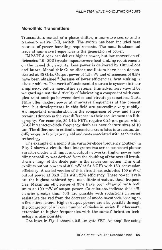
Monolithic Transmitters
Transmitters consist of a phase shifter, a mm -wave source and a transmit -receive (T R) switch. The switch has been included here because of power handling requirements. The most fundamental issue at mm -wave frequencies is the generation of power.
IMPATT diodes can deliver higher power, but low conversion ef- ficiencies (10-20%) would impose severe heat -sinking requirements on the monolithic circuits. Less power is delivered by Gunn -diode oscillators. Monolithic Gunn -diode oscillators have been demon- strated at 35 GHz. Output power of 1.5 mW and efficiencies of 0.5% have been obtained.6 Because of lower efficiencies, heat sinking is also a problem. The merit of fundamental sources in systems is their simplicity, but in monolithic systems, this advantage should be weighed against the difficulty of fabricating a component with com- plex relationships between device and circuit parameters. GaAs FETs offer modest power at mm -wave frequencies at the present time, but developments in this field are proceeding very rapidly. An important consideration in the comparison of' two- and three - terminal devices is the vast difference in their requirements in lith- ography. For example, 30-GHz FETs require 0.25-µm gates, while 37-GHz varactor-diode frequency doublers have feature sizes of 10 µm. The difference in critical dimensions translates into substantial differences in fabrication yield and costs associated with each device technology.
The example of a monolithic varactor-diode frequency doubler' in Fig. 7 shows a circuit that integrates two series -connected planar varactor diodes with input and output networks. Higher power han- dling capability was derived from the doubling of' the overall break- down voltage of' the diode pair in the series connection. This unit exhibits output powers of 300 mW at 24.8 GHz with 18% conversion efficiency. A scaled version of this circuit has exhibited 150 mW of output power at 36.9 GHz with 22% efficiency. These power levels are the highest achieved by a monolithic circuit at these frequen- cies. Maximum efficiencies of 35% have been obtained with both units at 100 mW of output power. Calculations indicate that effi- ciencies greater than 50% are possible with reductions in series resistance derived from the decrease of anode -to -cathode spacing to a few micrometers. Higher output powers are also possible through the connection of a larger number of diodes in series. Furthermore, extension to higher frequencies with the same fabrication tech- nology is also possible.
One inset in Fig. 1 shows a 0.5 -µm -gate FET. An amplifier using
RCA Review Vol. 46 December 1985 427

ILI cc. -c
IN OUT
SERIES CONNECTED BIAS NO. 1 VARACTOR DIODES
18.2 36.4 GHz
GHz
ti
RADIAL LINE STUB BIAS NO 2 Fig. 7-Monolithic frequency doubler with series connected diodes. The
module is 4 by 8 mm in size.
this device has exhibited 10 -dB gain at 16 GHz. Present efforts are devoted to the integration of this device in a monolithic amplifier and to achieving output power near 1 W, which is required by the frequency multipliers. Developments in this area have progressed rapidly. Monolithic amplifiers have demonstrated power levels of 100 mW at 28 GHz8 and 3 W at 8 GHz.9 Phase shifters at 16 GHz must have low insertion loss and can be designed using FET switches or GaAs PIN diodes. Another inset in Fig. 1 shows an example of a switched -line phase shifter under investigation. An- other alternative is an analog phase shifter using GaAs vat -actor diodes.
Insertion loss is even more detrimental in the case of a T/R switch. As a result, we are investigating the feasibility of planar GaAs PIN diodes such as the one shown in Fig. 8. Preliminary evaluation of three PIN diodes mounted in shunt across a section of fine line has shown insertion losses below 2 dB in the on -state and isolation in excess of 25 dB in the off -state from 26.5 to 40 GHz. This result has encouraged further work to improve the ohmic contacts of this de- vice and to achieve the eventual integration of PIN diodes in switching circuits.
GaAs PIN diodes currently under investigation have different designs. The vertical design is closest to conventional beam -leaded PIN diodes. The horizontal design10 is akin to the Si -PIN diodes
428 RCA Review Vol. 46 December 1985

MILLIMETER -WAVE MONOLITHIC CIRCUITS
Fig. E.-Planar GaAs PIN diode.
used in the bulk window diode array," where the novel device struc- ture has proven to be very successful.
In summary, the state of development of monolithic transmitters lags behind that of receivers, but the utilization of the existing monolithic technology base has resulted in considerable progress in a short period of time.
Conclusions
A large number of monolithic components, devices and processes have been developed in the course of these programs, many of which are first time demonstrations. These monolithic circuits indicate, for example, that the receiver functions can be achieved with three chips with a total area of 57 mm2 and a weight of 137 mg. Compared to hybrid circuits the reductions in size and weight are quite dra- matic. Cost reductions are possible through parallel batch pro- cessing when large -number units are produced.
Both the nature of the problems encountered and the anticipated benefits change as the design frequencies move from the microwave into the millimeter -wave regime. The need to incorporate diverse and novel circuits and devices becomes far more pressing, but on the other hand the resulting modules offer both improved perfor- mance and large reductions in size. The work at Lincoln Laboratory has elucidated these issues, and it is clear that monolithic compo- nents will be important elements in future mm -wave systems.
RCA Review Vol. 46 December 1985 429

References:
1 S. Mao, S. Jones and G. D. Vandelin, "Millimeter Wave Integrated Circuits," IEEE Trans. Electron Devices, ED -15, p. 517, 1968. 2 E. W. Mehal and R. W. Wacker, "GaAs Integrated Microwave Circuits," IEEE Trans. Electron Devices, ED -15, p. 513, 1968. 3 B. J. Clifton, G. D. Alley, R. A. Murphy, and I. H. Mroczkowski, "High Performance Quasi -Optical GaAs Monolithic Mixer at 110 GHz," IEEE Trans. Electron Devices, ED -28, p. 155, Feb. 1982. ° A. Chu, L. J. Mahoney, M. E. Ella, W. E. Courtney, M. C. Finn, W. J. Piacentini, and J. P. Donnelly, "A Two -Stage Monolithic IF Amplifier Utilizing a Ta2O5 Capacitor," IEEE Trans. Microwave Theory Tech., MTT-31, p. 21, Jan. 1983.
A. Chu, W. E. Courtney, and P. W. Sudbury, "A 31-G-iz Monolithic GaAs Mixer/ Preamplifier for Receiver Applications," IEEE Trans. Electron Devices, ED -28, p. 149, Feb. 1982. 6 N. Wang, S. E. Schwartz, and T. Hierl, "Monolithically Integrated Gunn Oscillator at 35 GHz," Electron. Lett., 20, p. 603, July 1984. 7 A. Chu, W. E. Courtney, L. J. Mahoney, R. W. McClelland, and H. A. Atwater, "GaAs Monolithic Frequency Doublers with Series Connected Diodes," 1984 IEEE Micro- wave & Millimeter -Wave Monolithic Circuits Symp. Digest, 29 May -1 June 1984, San Francisco, CA, pp. 74-77.
T. Noguchi, K. Suzuki, and H. Itoh, "28 GHz-Band GaAs Monolithic Amplifiers," 1984 GaAs IC Symp. Tech. Digest, 23-25 Oct. 1984, Boston, MA, pp. 192-196. 9 R. G. Freitag, J. E. Degendorf, D. G. Boire, M. C. Driver, R. A. Wickstrom, and C. G. Chang, "Wideband 3-W Amplifier Employing Cluster Matching," 1983 IEEE Micro- wave and Millimeter -Wave Monolithic Circuits Symp. Digest, 31 May -1 June 1983, Boston, MA, pp. 62-66. 10 H. Yang, private communication. 11 A. L. Armstrong, D. E. Wheeler, and J. Goodrich, "High Power Broadband, 35 GHz Switch Using a Monolithic Diode Array," 1984 IEEE International Microwave Symp. Digest, 30 May -1 June 1984, San Francisco, CA, pp. 400-401.
430 RCA Review Vol. 46 December 1985

GaAs FET MMIC Low -Noise Amplifiers for Satellite Communications*
H. -L. Hung, E. Enobakhare, J. Abita, P. McNally, C. Mahle, and H. Huang COMSAT Laboratories, Clarksburg, MD 20871
Abstract-One- and two -stage, X -band, low -noise, GaAs FET monolithic amplifier modules have been developed. These amplifier chips include all dc -blocking capacitors and bias networks. A cas- caded, two -chip, two -stage amplifier module provides a noise figure of 4 dB and an associated gain of 30 dB from 9.5 to 11.7 GHz. A two -stage 15 -dB gain block has also been developed for 9 to 13 GHz, with a chip size of 1.7 x 1.2 mm.
Introduction
Demand has been increasing for low -noise receivers and driver am- plifiers for commercial satellite communications, especially at X -
band frequencies. The frequency range from 10.7 to 12.7 GHz covers the international, domestic, and direct broadcast communications bands. The GaAs MMIC (monolithic microwave integrated circuit) approach offers the potential for lower -cost amplification modules and a significant reduction in component size compared to hybrid MIC modules. MMIC fabrication also provides performance unifor- mity, reduced phase variation, and potentially higher reliability.1-3 This paper describes the design considerations, fabrication process, and performance for the newly developed MMIC amplifier modules operating in X -band. These amplifiers can be used as driver ampli- fiers on board satellites, low -noise amplifiers II.NAs) in downlink earth station receivers, or functional gain blocks for general-pur- pose applications in satellite communications systems.
This paper is based on work performed at COMSAT Laboratories under the spon- sorship of the Communications Satellite Corporation.
RCA Review Vol. 46 December 1985 431

Device and Circuit Design
Design of these MMICs began with the development of an equiva- lent circuit model for the FET device. A recessed -gate, ri-FET con- figuration was chosen, with a nominal gate length and width of 0.7 p.m and 300 p.m, respectively. Fig. 1 shows a cross section of the FET structure. An in-house computer program for device modeling, COMFET, was used to generate the element values based on device physics, physical dimensions, and material parameters. Discrete de- vices were first fabricated to confirm the accuracy of the FET equiv- alent circuit model, given in Fig. 2, and the optimal source imped- ance for low -noise operation. The noise parameters of the device were also obtained through device measurements and an in-house least -mean -square -fit computer program.
One- and two -stage X -band LNAs were then designed using a distributed -element matching circuit approach. Figs. 3 and 4 are schematics of the one- and two -stage amplifier modules, respec- tively. Since all bias networks and dc -blocking capacitors at the input, interstage, and output were included in the design and circuit optimization, no further external components or additional tuning were needed for the amplifier evaluation. The sensitivity of the amplifier performance to device and material parameters was an- alyzed, and circuit matching elements were included in the design to identify and minimize performance deviation caused by pro- cessing variations. The overall size of the two -stage LNA module is 1.7 x 1.2 x 0.2 mm; the single -stage module has an area of 1.2 mm2.
6 um
Fig. 1-Cross section of Tr-FET structure.
432 RCA Review Vol. 46 December 1985

GaAs FET MMIC
1.2
R in ohms Capacitors in pF Gm in mho
0.04
Fig. 2-FET equivalent circuit model.
RF INPUT (50 it)
W.6 L = 3.2
W=2 L . 2.4
W=1 L . 6.8
W=2 L = 3.5
I
T
W=1 L = 38
0.711300 W2 Nm L = 4.5
W=7.5 L=14
DIMENSIONS IN mils CAPACITOR THICKNESS = 5,000 A
Fig. 3 -Schematic of one -stage amplifier module.
RE INPUT (50 0)
W.1 L-275
W.6 1-24
W -2 L.2
W.
W.2 L-3
0.7300 Pm W.1 W.2 W.2 W.2
L.14 l.1 L-1 L.5
L.31 - W.7.5 0 L.14
T 7n
DII,IENSIONS IN mils CAPACITORS NpF CAPACITOR THICKNESS - 5.000 A
Fig. 4 -Schematic of two -stage amplifier module.
1.62
W.1 L-3
0.7.300 W.1 pm -5
W-7.5 L.14
W=1 L = 24.3
W.1 L-2
RF
OUTPUT (50 5))
RE ¡--aOUTPUT
W-1 (50(t) L-15
RCA Review Vol. 46 December 1985 433

Fabrication Process
The MMICs were fabricated using ion implantation and optical lith- ography. Qualified 2 -inch -diameter unintentionally doped LEC wafers were selectively implanted with Si to form active regions. Both highly doped (N+ > 1018 cm -3) and moderately doped (N = 3 x 1017 cm -3) regions were formed at an implantation energy of 200 keV and 100 keV, respectively. The wafer was then annealed with a plasma -enhanced chemical -vapor -deposited silicon nitride (PECVD-Si3N4) cap at 850°C for 20 min. Ohmic electrodes for the FETs were formed by lifting off a Au-Ge-Ni-Ag-Au film and al- loying at 450°C for 1 min. A Ti/Al metalization was used to form gate structures up to 0.6 to 0.7 µm thick. Fig. 5 is an SEM photo- graph of the FET gate area.
Capacitors, crossovers, and passivation of components used the same dielectric material (silicon nitride), which was deposited (PECVD) to a thickness of 5,000 A, yielding a nominal value of 110 pF/mm2. The dielectric was patterned using reactive ion etching and photoresist masking. Dielectric was also used under the air -bridge crossover of capacitors for added protection against shorting, as il- lustrated in Fig. 6.
Two mask levels were employed to complete the fabrication of the metal -insulator -metal (MIM) capacitors and crossovers. Fig. 7 is an SEM photograph of the shunt -capacitor -to -ground used for rf bypass
101'M 20KV 00 000 S
Fig. 5-FET gate area.
434 RCA Review Vol. 46 December 1985

GaAs FET MMIC
-
10141 20KV 00 002
Fig. 6-Air-bridge crossover of a capacitor.
1OO1-N1 20K 00 008 S
Fig. 7-MIM rf bypass shunt capacitor.
RCA Review Vol. 46 December 1985 435

in the bias network. A series capacitor for do blocking and imped- ance matching is shown in Fig. 8. The two mask levels were also used to plate up the transmission -line metal thickness for low resis- tance. In this process, a base plating layer was evaporated using Ti/Au. The area to be gold-plated was opened by photolithographic technique and plated to 2 to 4µm thick. The wafer was then thinned to 0.2 mm, and the substrate side was metalized to com- plete the wafer process.
Measured Performance
After wafer fabrication, the MMICs were dc tested. The selected circuits were eutectically bonded to carriers which contained 50-L1
input and output transmission lines. The carriers were then mounted on test fixtures. Since all dc -blocking capacitors were in- cluded in the circuit design, no external bias tee was needed for amplifier evaluation.
Fig. 9 is a photograph of the single -stage module. When the bias is optimized for low -noise operation, a noise figure of 2.3 dB and an associated gain of 6.5 dB have been achieved at 11 GHz, as illus- trated in Fig. 10. Higher gain can be achieved at the expense of a higher noise figure.
For the two -stage MMIC LNA shown in Fig. 11, a power gain of 20 dB was achieved from 8.5 to 10 GHz under high -gain bias con-
--
2OF'M 20KV O04 S
Fig. 8-MIM dc -blocking series capacitor.
436 RCA Review Vol. 46 December 1985

GaAs FET MMIC
J
I
I
f
Fig. 9-Single-stage module.
10
t
r
10
3
2
11 12
FREQUENCY (GHz)
Fig. 10-Performance of one -stage MMIC LNA.
C
RCA Review Vol. 46 December 1985 437

Fig. 11-Two-stage module.
ditions, with gain decreasing to 10 dB at 13 GHz. The noise figure at low -noise bias in the same wide range is below 4 dB, with the best point of 3.4 dB occurring at 12.2 GHz (Fig. 12). By adjusting device and circuit parameters during fabrication, a broader band-
25
20
15
10
5
o
9 10 11
FREQUENCY (GHz)
Fig. 12-Performance of two -stage MMIC LNA.
12
4
3
2
438 RCA Review Vol. 46 December 1985

GaAs FET MMIC
25
20
m 15
z
c7 1 0
0 85 9.5 10.5 11.5 12.5 135
FREQUENCY (GHz)
l
I )
Fig. 13-Frequency response of a 9- to 13-GHz MMIC amplifier.
width performance with a power gain of 15 dB was achieved from 9 to 13 GHz, as illustrated in Fig. 13.
To achieve higher gain, two 2 -stage amplifier modules were cas- caded. A total gain of 30 ± 1 dB from 9.5 to 11.7 GHz and a noise figure of 4 dB were obtained. Fig. 14 shows the results of the cas- caded -module amplifier.
Conclusions
MMIC amplifier modules have been developed for X -band commu- nications satellite applications. Computer -aided design, ion implan-
50
40
m 30
z
20
10
_ 7
6
-1 5
4
0 I i 1 I 1
90 9.5 10.0 10.5 11.0 11.5 120
FREQUENCY (GHz)
Fig. 14-Performance of one -stage MMIC LNA.
RCA Review Vol. 46 December 1985 439

tation, and photolithographic processing techniques have been em- ployed to achieve the reported results. More recently, electron -beam direct -write technology has also been incorporated into the MMIC fabrication process to achieve shorter gate lengths, resulting in re- duced noise figures and improved power gain performance. These MMIC modules can be used for LNA or cascadable gain block appli- cations.
Acknowledgments
The authors would like to thank T. Smith, A. Ezzeddine, W. Chang, L. Holdeman, H. Carlson, F. Phillips, J. Singer, and R. Edwards for their contributions to the project.
References:
D. Ch'en and D. R. Decker, `Monolithic Microwave Integrated Circuits-the Next Generation of Microwave Components," Microwave J., 23(5), 67-78 (May 1980). 2 R. S. Pengelly, "Hybrid vs. Monolithic Microwave Circuits," Microwave Systems News, pp. 77-114 (Jan. 1983). 3 R. A.Pucel, "Design Consideration for Monolithic Microwave Circuits," IEEE
Trans. Microwave Theory Tech., MTT-29(6), 513-534 (June 1981).
440 RCA Review Vol. 46 December 1985

Recent Developments in Microwave GaAs FETs in Japan
Masumi Fukuta Microwave and High Speed Semiconductor Device Development Dapartment, Fujitsu Ltd., Kawasaki 211, Japan
Yasutake Hirachi Compound Semiconductor Laboratory, Fujitsu Laboratories, Atsugi, 243-01, Japan
Abstract-This paper reviews recent developments in microwave GaAs MESFETs in Japan. It introduces state of the art, in Japan, of the high -power GaAs MESFETs, the low -noise GaAs MESFETs, the low -noise high -electron -mobility transistors (HEMTs), and miniaturized circuit arrangements, such as the miniature hy- brid amplifier modules and the microwave monolithic inte- grated circuits (MMICs) for the consumer market.
An output power of 25 W at 6 GHz has been achieved from a high -power device with a 60.8 -mm gate width. Internally matched devices that can deliver 10 W at 1 -dB gain compres- sion with 8 -dB gain and more than 40% power -added efficiency at 8 GHz have reached production level. A novel via -hole plated heat sink (PHS) structure with improved gate -packing density is being developed for K -band GaAs power FETs. So is a 1.5- W 28-GHz FET amplifier using 4 -way splitter and combiner technology.
The low -noise MESFET with a 0.25-µm gate length exhibits a noise figure of 1.8 dB, with an associated gain of 9 dB at 18
GHz. On the other hand, the low -noise HEMT with a 0.5-µm gate gives a promising noise performance with noise figures of 1.4-1.7 dB and an associated gain of 9 dB at 18 GHz.
The miniature hybrid amplifier modules (CASPAC), which have a 5 -dB gain (with a ±0.3 -dB deviation) in the 6- to 18-GHz frequency range, are now commercially available. So are mi- crowave monolithic ICs for the consumer market that have noise figures of 1.7-2.2 dB, with 5 -dB gain in the frequency range from 50 to 1000 MHz.
RCA Review Vol. 46 December 1985 441

1. Introduction
Since the first commercially available low -noise GaAs MESFET was reported in 1974,1 Japan has been playing an important role in the development of GaAs devices for practical use. Why, in the absence of government or military support, was the first practical utilization of these devices successful in Japan? We think the fol- lowing reasons may be responsible: (1) the fact that the develop- ment for practical applications of this device began at an early stage, at least before 1970; (2) that there was a great need for re- placing the all -solid-state amplifiers for the TWTAs in the micro- wave radio -link systems; and (3) that there were some professional manufacturers of GaAs materials in Japan.
At present, Japanese industry is applying original and unique technologies to the GaAs technology. Recently, in addition to low - noise and power devices. GaAs ICs2 and new -structure FETs3 4 have been actively developed in Japan. This paper reviews recent devel- opments in the field of microwave GaAs FETs in Japan.
2. Power GaAs FET
Fig. 1 shows a 10 -year history5-1' of the development of power GaAs FETs since Fujitsu5 and RCA6 announced the first such devices in 1973. Nippon Electric Co. (NEC) reported 25 W at 6 GHz in 1980,9 the highest power achieved as of today. Fig. 2 shows a GaAs FET with a total gate width of 60.8 mm on a chip carrier with internally matched circuits.9 The size of the single -chip FET is 2.2 mm x 0.7 mm. The real part in the input impedance of the single -chip FET is 0.58 11 at 5 GHz. The low -loss capacitors were formed with a high - dielectric ceramic plate, whose principal component is BaO-Ti02. Its relative dielectric constant is 39, and its loss tangent, 2 x 10⁻⁴. Use of this capacitor made it possible to obtain good low -loss matching and phase uniformity within multichip devices. The output network consists of bonding wires and microstrip stubs formed on alumina substrates.
Fig. 3 shows input-output power characteristics of internally matched GaAs FETs with 60.8 -mm gate width.9 An output power of 25 W at 3 -dB gain compression and 5.8 GHz with 24% power - added efficiency were achieved.
Recent laboratory research has been concentrating on K -band de -
442 RCA Review Vol. 46 December 1985

ó
50
30
20
10
7
5 o 3
tx 2 W
0 a 1.0
0.7
I- 0.5
IL 0.3
0 0.2
0.1 2 3 5 7 10 20 30 50
JAPANESE GaAs FETs
FREQUENCY f (GHz) Fig. 1-Ten-year graph showing a history of the development of power
GaAs FETs.5-11 The symbols FJ and MT mean Fujitsu and Mitsu- bishi, respectively.
vices. Fujitsu developed a packaged 20-GHz 1-W device with a novel via -hole plated heat sink (PHS) structure."
Fig. 4 shows the cross-sectional view of a K -band GaAs FET with 1.2 -mm gate width and the novel via -hole PHS structure." The source -grounding pads, fabricated outside the active area, are di- rectly connected to the PHS through the holes made under these pads. The dimensions of the active area are 0.060 mm x 0.276 mm. Low source -lead inductances are necessary to obtain high gain, but the layout of the FET pattern should also be compact to prevent excessive phase difference between different parts of the FET. To this end, the novel via -hole PHS structure, as shown in Fig. 4, was developed.
Fig. 5 shows the SEM cross-sectional view of the completed novel via -hole PHS FET. The thickness of the GaAs substrate in this sample is about 10 p.m. The thickness of the plated heat sink is 35 p.m. In this sample, the width of a source -grounding pad was de- signed to be 53 p.m, and the bottom width of the via -hole was made approx. 35 p.m. The photograph illustrates that the bottom width of
RCA Review Vol. 46 December 1985 443

Fig. 2-A GaAs FET with a 60.8 -mm gate widtt- on a chip carrier with internally matched circuits.9
E CD
a_O
50 -
45
40
35
30
Wg(m^n) f(GHz) Vps(V)
60.8 5.8 II
o 30. 4 6.2 II x 60. 8 4. 1 II 8 6 4 dB
i/ / /
/ / / / / i
25 0 25 30 35 40
25W 20W
30
20 10
45
INPUT POWER P; (dBm )
Fig. 3-Input-output power characteristics of internally matched GaAs FETs with a 60.8 -mm gate width.9 An output power of 25 W at 3 -
dB gain compression and at 5.8 GHz with a power -added effi- ciency of 24% was achieved.
444 RCA Review Vol. 46 December 1985

JAPANESE GaAs FETs
SOURCE -FINGER
SOURCE -GROUNDING PAD
Via HOLE CONNECTIOI"
Fig. 4-Cross-sectional view of a K -band GaAs FET with a gate width of 1.2 mm and with the novel via -hole PHS structure. The source - grounding pads, fabricated outside the active area, are directly connected to the PHS through the holes made under these pads. The active area is 0.06 mm x 0.276 mm, and the ratio of gate width to active area (W9/Sa) is 66 mm -1.
a via hole can be as large as 53 p.m. This large etching tolerance is yet another feature of this novel via -hole structure.
Fig. 6 shows a 20-GHz rf test fixture having a stripline-waveguide transition. The waveguide is the WRJ-220. The sample mounted into the test fixture in Fig. 6 is a packaged 20-GHz 1-W novel via - hole PHS FET. Two chips of FETs with 1.2 -mm gate width are used in this package. The package consists of metal blocks except for the
Via HOLE CONNECTION
. - r ,, .- +_-.-.. I. w.. =/ -
P.H.S. Au --- SOpm
Fig. 5-Scanning electron microscopy photograph of the cross-sectional view of the completed novel via -hole PHS FET. The thickness of the GaAs substrate and the PHS in this sample are approx. 10 and 35 µm, respectively. In this sample, the width of a source - grounding pad was designed to be 53 µm, and the bottom width of a via -hole was made approx. 35 µm.
RCA Review Vol. 46 December 1985 445

,\111; . .,
5 P
'3 \
'2
Fig. 6-Photograph of a 20-GHz rf test fixture. The waveguide is the WRJ- 220. The sample mounted into the test fixture is a packaged 20- GHz 1-W novel via -hole PHS FET.
50-9 coaxial line through which pass the signals and dc bias sup- plies.
Fig. 7 shows the rf performance of the packaged novel via -hole PHS FET at 20 GHz. An output power of LOW (30 dBm) with 4.8 - dB gain and 13.1% power -added efficiency was obtained. These data show that, even at 20 GHz, space -qualified GaAs FETs'2 can be
made on a production scale. Mitsubishi developed a 1.5 lV 28-GHz FET amplifier based on the
4-way-splitter and combiner technology, as shown in Fig. 8.13 The transmission loss of the 4 -way combiner is less than 0.2 dB over a 27.5- to 28.4-GHz frequency range. The combining efficiency is higher than 90% (the combining loss is 0.6 dB) at 28 GHz (see Fig. 9).
As Fig. 1 shows, a race for the best data occurred in the 10 -year period between 1973 and 1983. However, as applications of power GaAs MESFETs increase, the following question arises: Which de- vice is the most useful one? We think that the most useful device will be the one having at a moderate, rather than a maximum power level, the highest gain and the highest power -added efficiency. Below we give an example of such a device that is now commercially available.
Fujitsu reported a device with 21.6 -mm gate width, capable of delivering 10 W at 1 -dB gain compression \\ith 8 -dB gain and 40% power -added efficiency at 8 GHz.'4 Fig. 10 shows an enlarged pho-
446 RCA Review Vol. 46 December 1985

JAPANESE GaAs FETs
E
v
PACKAGED
W9 2.4mm f = 20 GHz
VDS 10 V
18 20 22 INPUT POWER
24 P¡
0 a0
26 ldBm)
20
15
10
5
0
28
Fig. 7-Output power and power -added efficiency vs input power at 20 GHz for the packaged 2.4 -mm novel via -hole PHS FET with a 0.7- µm gate. These data show that, even at 20 GHz, the space -qual- ified packaged GaAs FETs15 are capable of being made on a pro- duction scale.
INPUT
4 -WAY SPLITTER
}
POWER 24 2 (dBm )
AMPLIFIER MODULE
}
18.0
4 -WAY COMBINER
}
26.0
}
31.8
OUTPUT
Fig. 8-Schematic diagram of a 1.5-W 28-GHz FET amplifier, which con- sists of four amplifier modules and a 4 -way splitter and com- biner.13
RCA Review Vol. 46 December 1985 447

35
30
FRED. 28 GHz
Po 25
100 20 (9 }
U " 90 Z EFFICIENCY - Z W
15 - 80 m
OW 10 70 OW
5 10 15 20 25
INPUT POWER P1 (dBm )
Fig. 9-Power transfer characteristics and combining efficiency of a 1.5- W 28-GHz FET amplifier.13
tograph of one corner of this chip. A newly developed tree -type feeder network provides an in -phase divided input signal to each gate finger.
Fig. 11 shows the internally matched device made from two FET chips, each with a gate width of 10.6 mm. These chips were used in a newly developed resonance -free package. The package has a
grounded metal sidewall and rectangular coaxial -type input/output, improving the isolation characteristics and ensuring stable opera- tion.
.;Ipl i
Fig. 10-Enlarged photograph of one corner ofthe C -band FET chip. A
tree -type feeder network provides an in -phase divided input signal to each gate finger.14
448 RCA Review Vol. 46 December 1985

JAPANESE GaAs FETs
Fig. 11-Internally matched device made from two FET chips with 10.6 - mm gate width. A new type of resonance -free package has a
grounded metal sidewall and rectangular coaxial -type input/ output terminals; this improves the isolation characteristics and ensures stable operation.
Fig. 12 shows rf characteristics of the two chips' internally matched devices.
Fig. 13 shows the measured third -order intermodulation distor- tion, IM3. At 33-dBm output power, IM3 was 41 dBc. Table 1 lists various internally matched devices that are now commercially available.
3. Low -Noise GaAs MESFET
As is well known, to get good noise performance from a GaAs MESFET, the series resistance, R,., must be reduced as much as possible. A conventional planar -type GaAs MESFET has a large Rs. On the other hand, an abruptly recessed type permits reducing the Rs. In this type, however, due to the contact of the gate metal with the side of the recessed region, the gate -fringing capacitance may become abnormally large. Also, the gate breakdown voltage may be low due to a very short effective gate -drain spacing.
RCA Review Vol. 46 December 1985 449

42
40
38
36
34
32
26 28 30 32 34
40 º v
20 0 ck`-
INPUT POWER Pi ( dBm )
Fig. 12-Input/output characteristics of the two chips' internally matched devices. The resulting device had an output power of 10 W at 1 -
dB gain compression and 8 -dB linear gain at 8 GHz with 40% power -added efficiency. This C -band higher -power device is now in production.
40
35
30
25
25 30
TWO-TONE INPUT POWER(dBm)
Fig. 13-Measured third -order intermodulation distortion, 1M3. At 33-dBm output power, 1M3 was 41 dBc.
450 RCA Review Vol. 46 December 1985

JAPANESE GaAs FETs
Table 1 -Various internally matched devices that are now commercially available.
PART NUMBER FREQUENCY POetlBtTyp.) GpoddBtyp)
FLM3742-4B 3.7 - 4.2 36 10 FLM3742-86 39 9 FLM4450- 46 4.4 - 5.0 36 9 FLM4450-8B 39 8
FLM5359 - 86 5.3 - 5.9 39 8
FLM5964-4C 5.9 - 6.4 36 9 FLM5964-8C 39 8 FLM6472-4C 6.4 - 7.2 36 8 FLM6472-8C 39 7
FLM7177-4C 7.1 - 7.7 36 8 FLM7177 -8C 39 7
FLM7785-4C 7.7 - 8.5 36 7 FLM7785-8C 39 6
FLM0910-2 9.5 - 10.5 33.5 7.5 FLM0910-4C 36 7.5 FLM I01 1 -2 10.7 - I 1.7 33.5 6 FLMI011-4C 36 6
FLMII I2 -4C 11.7 - I2.2 35.5 6
FLM 1212 -4C 12.3 - 12.8 35.5 5
FLM I 213 -4C 12.7 - 13.2 35.5 5
FLM I414 -2 14.0 - 14.5 33.5 4.5 FLM I4I 4 -4C 35.5 4.5
Therefore, NEC developed the gate recess structure shown in Fig. 14.15 In this structure, the transition in the thickness of the active layer from the gate to the source and drain is smooth, yet the shortest spacing between the effective source and gate is preserved. Experiments confirmed that this structure has almost the same gate -fringing capacitance and gate breakdown voltage as those of the conventional planar -type FETs. The gate, which was fabricated by the conventional deep UV/positive photoresist technology, is 0.3 µm long. A multilayer SiO2/Si3N4 passivation system produces highly reliable dc and rf characteristics and stable performance.
Fig. 15 shows the noise figure distribution of the newly developed MESFET at 12 GIIz.15 The distribution ranges from 1.2 to 1.5 dB, with a standard deviation of 0.08 dB.
RCA Review Vol. 46 December 1985 451

SOURCE GATE DRAIN
11- SI3N4
Si02
71 N CONTACT LAYER
N ACTIVE LAYER
P BUFFER LAYER
GOAS SUBSTRATE
Fig. 14-Cross-sectional view of a 0.3 -µm -gate low -noise GaAs MESFET.15 In this structure, there is a smooth transition in the thickness of the active layer from the gate to the source and drain, ensuring the reduction in R5, the smaller gate -fringing capacitance, and the higher gate breakdown voltage. The gate length of 0.3 p.m was defined by the conventional deep UV/positive photoresist technology. A multilayer SiO2/Si3N4 passivation system produces high -reliability characteristics.
Toshiba has developed low -noise GaAs MESFETs.16 Fig. 16 shows the schematic cross-sectional view of a 0.25 -p.m -gate GaAs FET. The gate length is defined by electron -beam lithography. The noise figure, F, and the associated gain, G0.. versus the drain current at 18 GHz are shown in Fig. 17. The optimal noise figure and the as- sociated gain were 1.8 ana 9 dB, respectively, at a drain current of 10 mA.
40
30
20
10
co = 1.40 dB
0 = 0.08 dB
N =130
1.2 1.3 1.4 1.5 1.6
OPTIMAL NOISE FIGURE Fo (dB)
Fig. 15-Noise figure distribution of the newly developed MESFET at 12
GHz.15 The best noise figure obtained was 1.2 dB.
452 RCA Review Vol. 46 December 1985

JAPANESE GaAs FETs
SOURCE
0.3 pm
trm
GATE
3 pm
-.1 pm
ACTIVE LAYE
0.25pm
BUFFER LAYER
0.5 pm
0.2 pm 0.8 pm
DRAIN
SEMI -INSULATING SUBSTRATE
I 1
1
Al
Pt / AuGe
Au / Pt / Ti
Fig. 16-Schematic cross-sectional view of a 0.25 -µm -gate GaAs FET de- veloped by Toshiba.16 The gate length is defined by electron - beam lithography.
4. Low -Noise HEMT
The performance of low -noise HEMTs has been promising. Fig. 18 shows the cross-sectional structure of a sample HEMT epi-wafer grown by molecular -beam epitaxy.17 The epitaxial layers consist of an undoped GaAs layer, several hundred nanometers thick, a 20- nm n+ -type Al03Ga0.7As layer, a 30-nm n-Al.Gai As layer, and a
6
4
2
0 O
f =18GHz VD5= 3 V
_-- Ga.
Vcf
-ao--p,
10 20 30 40
DRAIN CURRENT IDs (mA
Fig. 17-Noise figure, F, and associated gain, Gas, vs drain current at 18 GHz.16 The optimal noise figure obtained was 1.8 dB with a 9 -dB associated gain at los = 10 mA.
RCA Review Vol. 46 December 1985 453

50 nm N' - GaAs
30 nm N - Alx Gal_xAs
20 nm N+-AIGoi_xAs (x=0.3)
N=2x101ecm3
Undoped GaAs Electron layer
Semi - insulating GaAs substrate
Fig. 18 Cross-sectional structure of an example of an HEMT epi-wafer grown by molecular -beam epitaxy."
50-nm n' -GaAs layer. There is some dimensional electron gas in the undoped GaAs layer, just under the n+ -A10 3Ga0 7As layer. This two-dimenstional electron gas has a mobility of 26,000 cm2/V s at 77 K, and of 6000 cm2/V s at 300 K.
In the fabrication steps of the HEMT device, the selectively dry etching technique with CC12F2 gas plays an important role. Since the ratio of' the etching rate for AIGaAs to that for GaAs is 1/200, the etching process stops automatically just before the n -Al Ga1_xAs layer is reached.'8 Fig. 19 shows the typical drain I -V character- istics of an HEMT. The unit gate width is 50 µm, the total gate width is 200 µm, and the gate length is 0.5 µm. The maximum transconductance, g,,,. is 60 mS, which corresponds to 300 mS/mm. The reduction in g,,, shown in the higher gate -bias voltage region (Fig. 19) is thought to be caused by the carrier conduction in the neutral AIGaAs layer. Fig. 20 shows the noise figure and the asso- ciated gain of an HEMT at 19.6 GHz.'7 At the drain current of 10 mA, the optimal noise figure obtained was 1.7 dB, with an asso- ciated gain of 9 dB.
NEC developed a low -noise A1GaAs,GaAs FET with the p+ gate and the selectively doped structure.19 Fig. 21 shows the cross-sec- tional structure of such an FET. The gate is made with an Al - electrode and an interposed highly doped p+ -type GaAs thin layer. The p+ layer is introduced to reduce the source resistance and to achieve high reliability. The 0.5-µm gate is fabricated by means of conventional photolithography and the side -etch technique. Table 2 lists the device parameters and noise performance.
Toshiba developed a low -noise HEMT whose 0.4-µm Al -gate was defined by electron -beam lithography.20 Fig. 22 shows the data at
454 RCA Review Vol. 46 December 1985

JAPANESE GaAs FETs
© r tn,4
.0 M
2[I°i Inv
Fig. 19-Typical drain I -V characteristics of a low -noise HEMT." The total gate width, Wg, is 200 µm; the gate length is 0.5 µm. The max- imum transconductance, g,,,, is 60 mS, which corresponds to 300 mS/mm. The reduction in g,,, in the higher gate -bias voltage re- gion is thought to be caused by the carrier conduction in the neutral AIGaAs layer.
6
13 5
u_ 4
2
o 0 5 10 15 20 25 30
12
10
8
6
4
2
o
DRAIN CURRENT IDs (mA )
Fig. 20-Noise figure and associated gain of an HEMT at 19.6 GHz." The optimal noise figure obtained was 1.7 dB with an associated gain of 9 dB at a drain current of 10 mA.
RCA Review Vol. 46 December 1985 455

Source Gate
0.5-0.5-0.5 pm
Drain
- GaAs
n - GaAs
NA = 2x 1019cm 3
200 11
n AlxGar_xAs ND = 2x1o18cm-3 ( Graded ) 400 A
n - AID 3Gao.7As.
undoped AID 3Goo 7As 50 A
Fig. 21-Cross-sectional structure of a low -noise AIGaAs/GaAs FET with the p- gate.19 The p* layer was introduced to reduce the source resistance and to achieve high reliability.
'fable 2-Device parameters and noise performance of a low -noise AIGaAs/GaAs FET with the p- gate. A noise figu e of 1.2 dB at 12 GHz was obtained. with an associated gain of 11.7 dB.
R3 Rp gm
(Id= 10mA)
gd
(Id = 10mA)
Vp F,,(
4 GHz
G) 12 GHz
(f2) (I2) (mS) (mS) (V) (dB) (dB)
3.5 0.9 50 3.0 -0.7-1.4 0.34 (14.8 ) 1.2(11.7)
2
18 GHz
GO3
-
O 10 20
DRAIN CURRENT IDS (mA)
Fig. 22-Noise figure and associated gain of an HEMT having a 0.4 -µm - long gate.20 The optimal noise figure and the associated gain obtained at 18 GHz were 1.4 and 9 dB, respectively.
456 RCA Review Vol. 46 December 1985

JAPANESE GaAs FETs
18 GHz. At about IDS = 12 mA, a noise figure of 1.4 dB and an associated gain of 9 dB were achieved.
Comparing an HEMT with MESFET, we find the noise figure of an HEMT to be 0.4-0.5 dB lower than that of a MESFET.
5. Miniaturized Circuit Arrangements
Obviously, the monolithic microwave integrated circuit (MMIC) in- dustry requires a large market. At present, however, the market for MMICs is not very large, except for devices in a frequency range below 1 GHz. Further, wideband MMICs still face many unsolved design problems. For the next few years, therefore, it would appear more practical to promote hybrid microwave integrated circuits (HMICs). Below we introduce an example of an HMIC, as well as some unique technologies.
a. HMIC
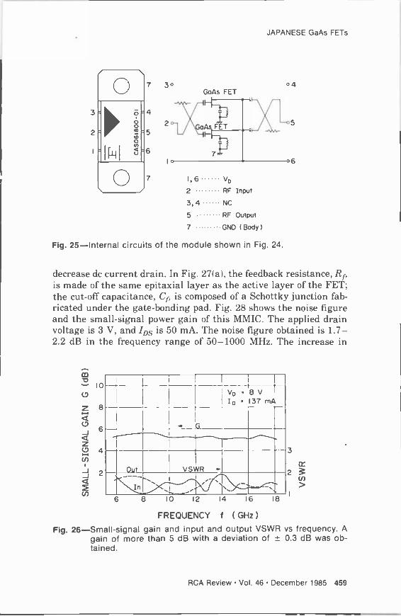
The HMIC, shown in Fig. 23, is a miniature balanced amplifier module based on thin-film technologies. The size of this module is almost the same as that of the conventional discrete FET. Fig. 24 shows the inside of the miniature amplifier module. There are 3 -dB couplers in both the input and output terminals. Since the input and output impedances are matched at 50 12, some amplifier mod- ules can be connected by cascading. This type of miniature amplifier has therefore been named the CASPAC (Cascadable and Packaged) amplifier.'= Fig. 25 shows the internal circuits of this module; Fig. 26 shows the small -signal gain and the input and output VSWR versus frequency. A gain of more than 5 dB with a ±0.3 -dB devia- tion was obtained. The CASPAC is now commercially available.
o b`/i ,.,:. , Fig. 23-Example of a miniature balanced amplifier module. The size of
this module is almost the same as that of the conventional dis- crete FET.
RCA Review Vol. 46 December 1985 457

i. .rrell! ._..._.....s -
f .
.. Psgi
!1'r.p1 M1 .
' I t CC.
I1 1
L__ ° - ' .. -4.1111-- 1.
Fig. 24-Inside view of the miniature hybrid amplifier module. Since the input and output impedances are matched at 50 12 by the use of 3 -dB couplers, some amplifier modules can be connected by cascading. This miniature amplifier has therefore been named the CASPAC (Cascadable and Packaged) amplifier.
b. MMIC
Finally, we are reporting a typical MMIC produced for the consumer market. As mentioned above, in the frequency range below 1 GHz, the MMIC is now available for industrial use.
Matsushita is producing UHF -band MMICs for TV tuners.22 Fig. 27(a) shows a top view of this MMIC, and Fig. 27(b) shows the circuit of the negative feedback amplifier used. R1, the feedback resistance, and C1, the capacitance, are included in the circuit to
458 RCA Review Vol. 46 December 1985
JAPANESE GaAs FETs
3
2
C \ /
7 30
4
5
6
7
GaAs FET
1, 6 Vo
2 RF Input
3,4 NC
5 RF Output
7 ..... GND (Body)
Fig. 25-Internal circuits of the module shown in Fig. 24.
04
decrease dc current drain. In Fig. 27(a), the feedback resistance, R1,
is made of the same epitaxial layer as the active layer of the FET; the cut-off capacitance, C. is composed of a Schottky junction fab- ricated under the gate -bonding pad. Fig. 28 shows the noise figure and the small -signal power gain of this MMIC. The applied drain voltage is 3 V, and /Ds is 50 mA. The noise figure obtained is 1.7- 2.2 dB in the frequency range of 50-1000 MHz. The increase in
10
8
4
2
Vo = 8 V
Io = 137 mA
3
2 In >
FREQUENCY f (GHz)
Fig. 26-Small-signal gain and input and output VSWR vs frequency. A
gain of more than 5 dB with a deviation of ± 0.3 dB was ob- tained.
RCA Review Vol. 46 December 1985 459

(a)
(b) Fig. 27-Example of an MMIC for the consumer market21: (a) Top view of
the completed MMIC and (b) circuit of the negative feedback am- plifier used.
noise in the frequency below 100 MHz appears to be caused by the 1/x noise.
6. Summary
We have reviewed recent developments in microwave GaAs FETs in Japan. Devices covered are high -power GaAs MESFETs, low - noise GaAs MESFETs, low -noise high -electron -mobility transistors (HEMTs). and miniaturized circuit arrangements, including min- iature hybrid amplifier modules (HMICs) and MMICs.
An output power of 25 W at 6 GHz was achieved from a high - power device having a gate width of 60.8 mm. Internally matched devices capable of delivering 10 W at 1 -dB gain compression with an 8 -dB gain and a power added -efficiency greater than 4074 at 8
460 RCA Review Vol. 46 December 1985

6
5
4
3
2
0 20 50 100 200
JAPANESE GaAs FETs
10
5
500 1000 2000 o
5000
FREQUENCY f ( MHz)
Fig. 28-Noise figure and small -signal power gain of the MMIC.21 The noise figure obtained was 1.7-2.2 dB in a frequency range of 50-1000 MHz.
GHz are now in production. A novel via -hole plated heat sink (PHS) structure with an improved gate -packing density was developed for K -band GaAs power FETs. A 1.5-W 28-GHz FET amplifier based on 4 -way splitter and combiner technology was developed.
The low -noise MESFET with a gate length of 0.25 p.m had a noise figure of 1.8 dB with an associated gain of 9 dB at 18 GHz. On the other hand, the low -noise HEMT with the 0.5-µm gate showed promise, having noise figures of 1.4-1.7 dB and a 9 -dB associated gain at 18 GHz.
Miniature hybrid amplifier modules (CASPAC) having a 5 -dB gain and a gain deviation of ±0.3 dB in the 6- to 18-GHz frequency range are now commercially available. So are microwave monolithic ICs (MMICs) for the consumer market; these have noise figures ranging from approximately 1.7 to 2.2 dB, with a 5 -dB gain in the 50- to 1000 -MHz frequency range.
Ever since the first commercially available GaAs MESFET was reported in 1974, Japan has been consistantly supplying the best - performance devices. Recently, not only low -noise and power de- vices, but also GaAs ICs and new -structure FETs have been devel- oped in Japan. In the future, Japan will continue supplying various types of GaAs devices.
RCA Review Vol. 46 December 1985 461
Acknowledgments
The authors wish to thank Dr. A. Higashisaka and Dr. K. Ohata of NEC, Dr. T. Suzuki of Mitsubishi, Dr. K. Kamei of Toshiba, and Dr. S. Nambu of Matsushita for contributing some data and tech- nical information.
References:
1 K. Ohata and M. Ogawa, "Degradation of gold -germanium ohmic contact to N - GaAs," 12th Annual Proc. Reliability Physics, 1974, pp. 278-283. 2 N. Yokoyama, H. Onodera, T. Shinoki, H. Ohnishi, and H. Nishi, "A 3 ns GaAs 4 K x 1 B Static RAM," IEEE Trans. Electron Devices, ED -32, 1797-1801 (Sept. 1985).
3 T. Mimura, S. Hiyamizu, T. Fujii. and K. Nambu, Japan J. Appl. Phys. Lett., 19, L225-L227 (1980). 4 N. Kobayashi, S Natomi, M. Suzjki, T. Tsuchiya, K. Nishiuchi, K. Odani, A. Shi- batomi, T. Mimura, and M. Abe, "A fully operational 1 Kb HEMT Static RAM," Proc. IEEE Gallium Arsenide Integrated Circuits Symp.-GaAs IC, Monterey, CA, Nov. 12-14, 1985. pp. 207-210. 5 M. Fukuta, T. Mimura, I. Tsujimura, and A. Furumoto, "Mesh -source type micro- wave power FET," IEEE Int. Solid -State Circuits Conf. Tech. Dig., pp. 84-85, 1973. 6 L. S. Napoli, R. E. DeBrecht, J. J. Hughes, W. F. Reichert, A. Dreeben, and A. Triano, "High -power GaAs FET amplifier-A multigate structure," IEEE Int. Solid - State Circuits Cont. Tech. Dig., pp. 82-83. 1973. 7 W. C. Niehaus, H. M. Cox, B. S. Hewitt, S. H. Wemple, J. V. DiLorenzo, W. O. Schlosser, and F. M. Magalhaes, "GaAs Power MESFETs," Proc. 5th Int. Symp. GaAs and Related Compounds, St. Louis, MO, 1976, pp. 271-280.
8 M. Fukuta, T. Mimura, H. Suzuki, and K. Suyama, "4-GHz 15-W Power GaAs MESFET," IEEE Trans. Electron Devices, ED -25 559-563 (June 1978). 9 A. Higashisaka, Y. Takayama, and F. Hasegawa, "A high -power GaAs MESFET with an experimentally optimized pattern," IEEE Trans. Electron Devices, ED -27, 1025-1029 (June 1980). 10 Y. Mitsui, M. Kobiki, M. Watanabe, K. Segawa, M. Otsubo, and T. Ishii, "10 GHz 10 W internally matched flip -chip GaAs power FET"s," IEEE Trans. Microwave Theory Tech., MTT-29, 304-309 (April 1981). 11 Y. Hirachi, Y. Takeuchi, M. Igarashi, K. Kosemura, and S. Yamamoto, "A pack- aged 20-GHz 1 -W GaAs MESFET with a novel Via -Hole plated heat sink structure," IEEE Trans. Microwave Theory Tech., MTT-32 309-316 (March 1984). 12 B. Dornan, W. Slusark, Jr., Y. S. Wu, P. Pelka. R. Barton, H. Wolkstein, and H. Huang, "A 4-GHz GaAs FET power amplifier: An advanced transmitter for satellite downlink communication systems." RCA Rev., 41(3), 472-503 (Sept. 1980). 13 T. Takagi K. Seino, Y. Ikeda, O. Ishihara, and F. Takeda, "A 1.5 watt 28 GHz band FET amplifier,"/EEE Microwave Theory Tech. Symp., Tech. Dig. pp. 227-228, 1984. 14 J. Fukaya, M. Ishii, M. Matsumoto, and Y. Hirano, "A C -band 10 watt GaAs power FET," IEEE Microwave Theory Tech. Symp., Tech. Dig., pp. 439-440, 1984. 15 H. Ishiuchi, H. Mizuno, Y. Kaneko, K. Arai, and K. Suzuki, "0.3 µm gate length super low noise GaAs MESFET," IEEE Int. Electron Devices Meeting, Tech. Dig., pp. 590-593, 1982. 16 K. Kamei, S. Hori, H. Kawasaki, T. Chigira, and K. Kawabuchi, "Quarter micron low noise GaAs FET's operable up to 30 GHz," IEEE Int. Electron Devices Meeting, Tech. Dig., pp. 102-105, 1980. 17 K. Joshin, Y. Yamashita, M. Niori, J. Saito, T. Mimura, and M. Abe "Low noise HEMT with self -aligned gate structure," Proc. 16th Conf. on Solid -State Devices and Materials. 1984, pp. 347-350.
462 RCA Review Vol. 46 December 1985

JAPANESE GaAs FETs
18 K. Hikosaka, T. Mimura, and K. Joshin, "Selective dry etching of AIGaAs-GaAs heterojunction," Japan. J. Appl. Phys., 20, L847-L850 (Nov. 1981). 19 K. Ohata, H. Hida, H. Miyamoto, M. Ogawa, T. Baba, and T. Mizutani, "A low noise AIGaAs GaAs FET with P' -gate and selectively doped structure," IEEE Microwave Theory Tech. Symp., Tech. Dig., pp. 434-436, 1984. 20 K. Kamei, S. Hori, H. Kawasaki, K. Shibata, H. Mashita, and Y. Ashizawa, "Low noise high electron nobility transistor," Proc. 11th Int. Symp. GaAs and Related Compounds, Biarritz, France, Sept. 1984, pp. 545-550. 21J. Browne, "Miniature amplifier meets transistor size requirements," Microwaves & RF, 22(7), 114-119 (1983). 22 M. Nishiuma, K. Kanazawa, M. Hagio, and S. Nambu, "GaAs monolithic low -noise wideband amplifier," Nat. Tech. Rep. 29, 71-79 (April 1983).
RCA Review Vol. 46 December 1985 463

Miniature Microwave Hybrid Circuits- Alternative to Monolithic Circuits*
Erwin F. Belohoubek RCA Laboratories, Princeton, NJ 08540
Abstract-A new fabrication technology for miniature microwave hybrid circuits and the application of these circuits to a variety of microwave components and subsystems is described. These thin-film batch -processed circuits offer the advantages of very small size, light weight, and low loss, together with the possi- bility of combining several functions on a common substrate. Excellent rf performance has been demonstrated in power am- plifiers as well as receiver components, including a complete transmit/receive module.
1. Introduction
For most modern microwave systems, especially in the areas of radar, communications, or EW applications, there are strong incen- tives for making the circuits as small and light as possible while maintaining high performance standards. Microwave hybrid inte- grated circuits, which have nearly completely replaced the old bulky waveguide components, are now being challenged by two new com- peting technologies, monolithic microwave integrated circuits and various forms of miniature microwave hybrid circuits. Monolithic circuits have been widely analyzed and described in the litera- ture,1-3 but comparatively little has been published recently about miniature hybrid circuits.
Pioneering work on lumped -element microwave components was carried out at RCA Laboratories in the early 197Os. During this period much of the foundation was laid for the processing of thin -
The research described herein was partially supported by the Department of the Army, U.S. Army Advanced Concepts Team, under Contract DAAK20-82-C-0129 and the INTELSAT Organization under Contract INTEL -350.
464 RCA Review Vol. 46 December 1985

MINIATURE MICROWAVE HYBRID CIRCUITS
film lumped -element circuits and their microwave characteriza- tion.4-6 A strong renewed effort during the last few years led to RCA's Miniature Beryllia Circuit Technology which originally was tailored specifically towards GaAs power FET applications. More recently, we also began exploring the extension of this technology to low -power applications such as tunable oscillators, receiver cir- cuits, and phase shifters. This paper concentrates on these recent advances and provides a variety of examples that demonstrate the excellent capabilities of this new technology.
Before proceeding with a more detailed description of miniature hybrid circuits, it is useful to review the properties and advantages and disadvantages of today's three major microwave circuit fabri- cation technologies, which are summarized in Table 1. The majority of components today are still being built in standard hybrid form with the attending disadvantages of bulkiness, high assembly labor content, and relatively high cost, even where large quantities are required. Due to the large number of separate interconnections, in
Table 1-Comparison of Microwave Circuit Fabrication Technologies
Standard Hybrid Circuits Separate circuit substrates interspersed with active devices, often in packaged
form \Vire bonds and solder strap interconnects Good rf performance Tuning and trimming readily possible Low nonrecurring engineering costs Somewhat bulky and heavy High assembly labor content Mainly for small to moderate quantities
Monolithic Circuits Active devices and circuits components integrated in the same substrate More than one function can be combined on a common substrate Very small, lightweight Best suited for high -volume production Batch process promises ultimately low cost and high reliability RF performance generally poorer, especially NF and efficiency; bandwith may be
better Unfavorable active-deviceicircuit-area ratio
Miniature Hybrid Circuits Circuit substrates thin-film hatch processed Active devices added separately in chip form Flexibility-variety of devices can be combined on a common multifunction
substrate Use of thin-film lumped -element components makes size and weight comparable
to monolithic circuits Choice of substrate for high- or low -power applications Excellent heat dissipation and high Q achievable with BeO Pretesting of circuits possible. high yield Potentially low fabrication cost: moderate nonrecurring engineering costs
RCA Review Vol. 46 December 1985 465

the form of wire bonds or solder straps, the reliability of these com- ponents depends to a large degree on the skill of the assembly labor. However, these circuits do work and offer good rf performance; fur- ther, their processing requires only relatively small capital outlays.
Monolithic circuits, strongly in the news forefront of recent years, were to overcome most of the drawbacks of the standard hybrid circuits. Unfortunately, these circuits have their own peculiar prob- lems and disadvantages, such as low efficiency, poor heatsinking, and ineffective use of expensive substrate area. The most promising results have been obtained in ultrawideband amplifiers where par- asitic reductions lead to excellent performance, albeit with conces- sions in efficiency, noise figure, and power output. The promise of low-cost fabrication for monolithic circuits will be elusive for some time to come until a truly large volume market becomes a reality.
The miniature hybrid circuits are an attempt to combine the ad- vantages of monolithic circuits with those of the standard hybrid circuits while minimizing the disadvantages of both. This tech- nology is based on the batch processing of circuits using a mixture of thin-film lumped -element or distributed components similar to those used in the monolithic approach, with the exception that ac- tive devices are added separately to the circuit substrate after it is completed and tested. The resulting circuits are comparable in size and weight to monolithic circuits but offer the following additional advantages:
Design flexibility: Circuit and device substrates can be chosen independently for best performance. A variety of different devices (GaAs FETs, Si bipolar transistors, varactors, and PIN diodes) can be integrated on the same substrate. Optimum performance: Circuit substrates can be selected for high Q and excellent heat conductivity where needed; special low -in- ductance grounds can be integrated throughout the substrate. Low cost in moderate quantities: Circuits can be conveniently batch processed and tested separately. Ultimate cost is dominated by the cost of the active devices.
Obviously, there is no single, unique technology that is ideally suited for all microwave applications. Rather, the most successful system design will make use of a variety of technologies wherever a definite advantage in cost, performance, reliability or convenience in fabrication is apparent. Early examples of miniature hybrid tech- nology are the low -noise and low -power amplifiers manufactured by Avantek. Individual amplifier stages are batch -processed using thin-film lumped -element matching structures, with devices in chip
466 RCA Review Vol. 46 December 1985

MINIATURE MICROWAVE HYBRID CIRCUITS
form subsequently mounted and bonded to the circuits. This type of miniature hybrid technology has been successfully applied to am- plifiers from L- to Ku-band.7.8 In power amplifiers, thick -film me- tallized BeO with partial matching elements has been used as a substrate for internally matched miniature GaAs FET amplifiers.9 Ground contacts for the devices and matching elements are usually provided by wrap -around metallization and sometimes by via holes. A more advanced process technology that is suited for a wide variety of applications and able to combine several functions on a common substrate is based on RCA's Miniature Beryllia Circuit (MBC) tech- nology.') It is this process and its more recent low -power derivative'' that are discussed in this paper.
2. Process Technology for Miniature Hybrid Circuits
RCA has recognized the need for a high-performance miniature hy- brid circuit medium for some time and during the last few years has developed a new technology (MBC) that is especially tailored to the requirements of high -efficiency, batch-processable power ampli- fier circuits.
Fig. 1 shows a typical substrate strip that contains 10 two -stage X -band power amplifier circuits. Excellent heat -dissipation capa- bility, good reproducibility, low loss, small size, and low weight are the key features of this process. The circuits contain all rf matching elements, dc bias lines, and resistors, with only the active devices to be added in a final assembly step. A special process permits the inclusion of copper septa into the substrate to provide low -parasitic ground returns for the active devices. Whenever possible, devices with suitable bump contacts are used to permit flip -chip mounting. Regular mounting of devices, i.e., with the substrate down, is also possible, although this requires additional wire bonds for intercon- necting the device with the circuitry. Flip -chip -mounted devices
a a
] ar
-
EE
- at - az L
-BE =' -- =
_)
L . E - rE E 9= t E G
- aC
L aL - _al - j C L L a= G L L I' L
IIIIIIIII 1 INCH
Fig. 1-MBC substrate containing 10 two -stage power amplifier circuits.
RCA Review Vol. 46 December 1985 467

have the advantages of better heat dissipation, easier assembly, and higher reliability due to the elimination of wire bonds.
For power applications, BeO serves as the circuit substrate, of- fering excellent thermal conductivity, low rf losses, and a thermal expansion coefficient that matches closely that of GaAs. For low - power applications, alumina can replace BeO, which greatly sim- plifies the cutting and polishing steps of the substrate preparation and lowers the overall circuit cost. The fabrication process for a typical MBC power amplifier stage starts with the preparation of the BeO substrate, which includes a septum for low -inductance ground returns. For a single septum structure, two BeO plates, each of which has been copper metallized on one side, are bonded together in a fixture under high temperature and pressure. The solid diffusion between the copper layers forms a very strong ther- mocompression bond. If an application requires multiple stage am- plifiers with multiple septa, the process allows the number of ce- ramic wafers and their thicknesses to be adjusted to any desired design configuration.
After thermocompression, the sandwich is sliced, as shown in Fig. 2, into individual strips of appropriate thickness and the slices are then polished. Since the surface of even highly polished ceramic substrates is generally not smooth enough to ensure a good yield of capacitors with high -voltage breakdown, a smoothing layer such as glass or polyimide is required. The glaze, applied selectively, covers
SEPTUM
0.010 to 0.020 in.
T-
UP TO 2 in.
TYPICALLY 0.100 TO 0.250 in.
BeO or A1203
Fig. 2-BeO-Cu-BeO sandwich (first step in MBC substrate fabrication).
468 RCA Review Vol. 46 December 1985

MINIATURE MICROWAVE HYBRID CIRCUITS
only the essential circuit areas; the metal septum and its immediate surroundings remain uncovered to provide a suitably metallized bonding area for the active device, in many cases a GaAs FET. The next step in the process involves batch -fabricating matching circuits consisting of a mixture of lumped and distributed elements, to- gether with bias networks, onto the substrate strips, as shown in Fig. 3. This is followed by pretesting the strips, dicing them into individual circuits, and then flip -chip bonding the active devices above the septum area. At present, two other companies besides RCA, Mitsubishi and MSC, fabricate GaAs FET power devices with suitable bump configuration for flip -chip mounting. Both thermo- compression and solder reflow are used successfully to mount these devices.
Fig. 4 shows a cross section of the completed circuits in more detail. A thin-film base conductor forms the ground contacts, the bottom electrodes of the capacitors, inductive lines, and the first level of interconnections. The capacitor dielectric generally is a thin layer of sputtered silicon nitride. Another metal layer forms the second layer of interconnections, a second metal layer for the in- ductors, and the top electrodes for the capacitors. Plated bridges over a polyimide insulating layer make contact to capacitors. This
Be0
Tuning Circuits
FET Pellet
FET Pellet_ Flip-Chip Bonded"\
GLAZED Be0 STRIP
BATCH-FABRICATED CIRCUITS
,-Contact / Bumps
FET ASSEMBLY
Complete Amplifier
Fig. 3-MBC fabrication process.
RCA Review Vol. 46 December 1985 469

AIR BRIDGE TOP Si3N4
GLASS
FET CONNECTING BONDS
% y BASE R CONDU \/j /: 'í.atari.: 6 ',
Be0
Fig. 4-MBC structure detail.
COPPER SEPTUM
very reproducible arrangement eliminates the need for extra wire bonds and solves voltage -breakdown problems that normally occur at the edges of the dielectric layers of capacitors. It also allows termination and bias resistors to be integrated in the form of a Cermet under the base conductor layer.
A major advantage of this technology is its low circuit loss. High - Q inductors can readily be formed on both BeO or A1203 substrates. Contrary to monolithic substrates, which must remain rather thin (50 to 100 µm) for heat dissipation reasons, miniature hybrid cir- cuits permit the use of optimum substrate thickness for the for- mation of high -Q inductors and low -loss transmission lines.
The fabrication process described so far has concentrated on sub- strate wafers capable of having active devices mounted on the top surface. However, a large number of devices, either low -noise or low -power, do not have the proper bump contacts for flip -chip mounting. It is possible to mount such devices on top of the sub- strate with interconnections formed by wirebonds. For very high frequencies, however, where interconnect parasitics become quite influential, the modified substrate fabrication process shown in Fig. 5 may be better suited. Here, a recess generated in the substrate lowers the active device into a hole and thereby greatly reduces parasitic inductances. The fabrication is similar to that of the reg- ular substrate with multiple septa except that it includes grooving the starting wafers where the final substrate will have a hole.
3. Application Examples of Miniature Hybrid Technology 3.1 High -Efficiency Amplifiers
For many of today's spaceborne communications systems, traveling - wave tubes together with reflector antennas serve as rf transmitters to ground. Recent advances in GaAs FETs promise to replace this
470 RCA Review Vol. 46 December 1985

MINIATURE MICROWAVE HYBRID CIRCUITS
GROOVE
(o) ---=F-Z-4..
III
CERAMIC PLATES
CERAMIC PLATE
THROUGH HOLES
METAL SEPTUM \,
(c) THERMOCOMPRESSION BOND
Fig. 5-Fabrication of ceramic substrates with septum and holes.
METAL COATING
(b)
7-SUBSTRATE
CUTS
BONDED PLATES
type of system with a large number of solid-state moderate -power
amplifiers directly integrated with the radiating elements of an
active array antenna.12 The key amplifier requirements are very
low weight, small size, high operating efficiency, high reliability, and low fabrication cost.
The one- and two -stage amplifiers described here fulfill all of
these objectives. The designs, based on MBC technology and opti-
mized for high efficiency, result in very small size, good reproduc- ibility, and the potential for large -volume batch fabrication. Fig. 6
shows a closeup of a single amplifier stage. A 1-W FLX102 FET
pellet ís mounted substrate -down at the center of the metal pattern with the source grounded through the septum. Short inductive lines,
RCA Review Vol. 46 December 1985 471

.
Fig. 6-Single-stage power amplifier on BeO.
arranged in pairs, and Si3N4 capacitors connected to ground form the input and output tuning circuits. Selecting different capacitors allows tuning the band center over approximately 1 GHz.
The optimization procedure was simplified by extensive use of a computer -aided efficiency -optimization setup together with load - pull measurements. Fig. 7 shows the amplifier performance when
700. 0r
620. 0:..
500. 0 E
400.
300. 0_ rt w
200. OP -
100.0E_
/
5.9 dB
P out
EFF
4.3 dB
45
40 1^
20 W
CC
10 3 o a
1.2 dB Frequency = 12.76 GHz
1L1LL11J111-11 1 i i l I,.L1 11 l 11 t O. 0 o o m o s m m o o o m o
O Vf O Ifl p VI U N O I!1 B N N
^ ^ ^ N N N
POWER IN (mW)
Fig. 7-Single-stage power amplifier performance.
472 RCA Review Vol. 46 December 1985

MINIATURE MICROWAVE HYBRID CIRCUITS
adjusted for maximum efficiency at a moderate power level. An efficiency of 42% was obtained with 500-mW power and 5.9 -dB gain. These values include input and output connector losses that are typically 0.2 dB each at 12 GHz. With direct integration of the amplifier into the antenna element, power -added efficiencies in ex- cess of 45% are feasible at 12 GHz, using commercially available GaAs FETs in chip form. Due to the operation of the FET well below its maximum rated output and the excellent heatsinking of the de- vice, the operating temperature is low, resulting in long life expec- tancy.
A more advanced multiple -stage power amplifier is shown sche- matically in Fig. 8. The amplifier consists of a driver stage that feeds two paralleled power amplifiers combined by interdigitated couplers. All components, including matching circuits, bias lines, bypass capacitors, and couplers, are thin-film deposited on a common two -septa BeO substrate. The devices, Mitsubishi GaAs FETs type MGFC 2124, are flip -chip mounted, eliminating a large number of wire bonds and thus greatly contributing to the repro- ducibility and reliability of the overall amplifier.
At present, four complete amplifier circuits are processed simul- taneously as shown in Fig. 9. Multisepta substrates fabricated from 2 x 2 -inch wafers are expected to increase the number of complete amplifiers fabricated together by at least an order of magnitude. Similarly, the 50-l1 termination resistors for the couplers that cur-
TERMINATION
FREQUENCY RANGE 11.7-12.2 GHz
BeO SUBSTRATE
Fig. 8-Two-stage 12-GHz power amplifier.
RCA Review Vol. 46 December 1985 473

Fig. 9-Strip of two -stage amplifier circuits.
rently are still added separately to the finished circuit will he inte- grated in the form of Cermet resistors as part of the standard depo- sition sequence.
The performance of the two -stage miniature power amplifier is shown in Figure 10. A power output of more than 1.6 W is obtained over the full 11.7- to 12.2-GHz band with a gain in excess of 10 dB. The power -added efficiency is approximately 30%. Excellent heat conduction, good reproducibility, and very small size (0.22 x 0.36 inch) are the key features of this amplifier. It forms thus an excel- lent building block for large -N combiner structures aimed at the replacement of power traveling -wave tubes.
20
19
18
17
16
15
14
13
12
Pin=160mW
27
10 25 117 118 I19 120 121 122
FREQUENCY (GHz1
Fig. 10-Two-stage power amplifier performance.
474 RCA Review Vol. 46 December 1985

MINIATURE MICROWAVE HYBRID CIRCUITS
3.2 Medium Power and Low -Noise Amplifiers
Although the original batch process was developed for BeO sub- strates, it is equally applicable to other substrate materials. For lower -power application, alumina is in many cases perfectly ade- quate to provide the necessary heatsinking for the active devices. Alumina has the advantages of being considerably lower in cost and not requiring special safety precautions in grinding. A good ex- ample of the miniature lumped -element hybrid technology applied to a two -stage low -power amplifier]] is shown in Fig. 11. The alu- mina substrate incorporates two septa to provide low parasitic grounding between stages. Since low -power GaAs FETs presently are not being fabricated with bumps suitable for flip -chip mounting, the devices must be mounted substrate down. We found it desirable in many cases to reduce the parasitics of the required wire bonds by recessing the devices into a hole in the substrate as shown in Fig. 11. Alternatively the devices can he mounted directly on top of the septum metallization.
The amplifier was designed as part of a high -gain i -f amplifier for the 3.7- to 4.2-GHz range. Negative feedback is incorporated into each stage to equalize gain and ease the cascading of stages. The white rectangular elements visible in Fig. 11 are negative feed -
0.300 7,6mm
1rt
fr J . fl l I
¡ . l u I
".-
0 230" 5,8 mm
Fig. 11-Two-stage C -band low -power amplifier.
RCA Review Vol. 46 December 1985 475
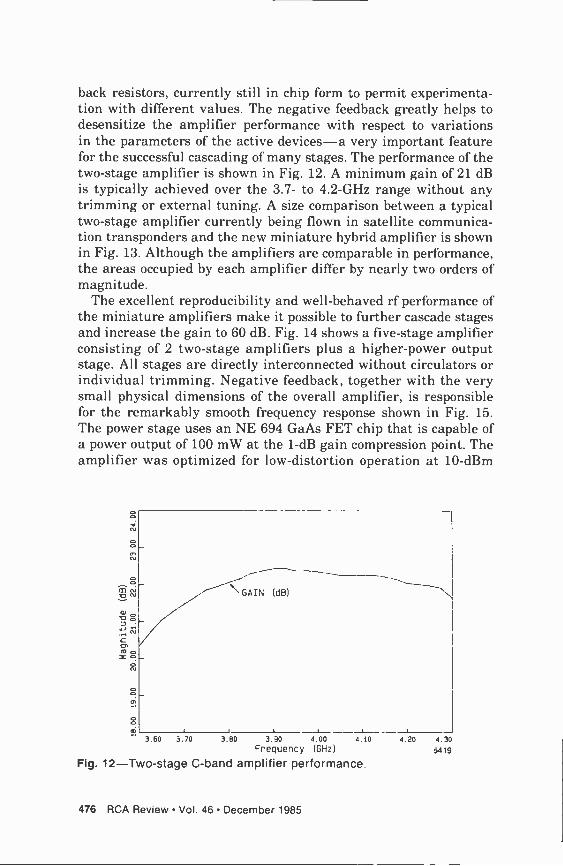
back resistors, currently still in chip form to permit experimenta- tion with different values. The negative feedback greatly helps to desensitize the amplifier performance with respect to variations in the parameters of the active devices-a very important feature for the successful cascading of many stages. The performance of the two -stage amplifier is shown in Fig. 12. A minimum gain of 21 dB is typically achieved over the 3.7- to 4.2-GHz range without any trimming or external tuning. A size comparison between a typical two -stage amplifier currently being flown in satellite communica- tion transponders and the new miniature hybrid amplifier is shown in Fig. 13. Although the amplifiers are comparable in performance, the areas occupied by each amplifier differ by nearly two orders of magnitude.
The excellent reproducibility and well-behaved rf performance of the miniature amplifiers make it possible to further cascade stages and increase the gain to 60 dB. Fig. 14 shows a five -stage amplifier consisting of' 2 two -stage amplifiers plus a higher -power output stage. All stages are directly interconnected without circulators or individual trimming. Negative feedback, together with the very small physical dimensions of the overall amplifier, is responsible for the remarkably smooth frequency response shown in Fig. 15. The power stage uses an NE 694 GaAs FET chip that is capable of a power output of 100 m«' at the 1 -dB gain compression point. The amplifier was optimized for low -distortion operation at 10 -am
/GAIN (dB)
Q1 p Y N 0
o o
01
o 1 1
3.60 3.70 3.60 3.90 4.00 4.10 4.20 4.30
Frequency (GHz) 5419
Fig. 12-Two-stage C -band amplifier performance.
476 RCA Review Vol. 46 December 1985

MINIATURE MICROWAVE HYBRID CIRCUITS
( o E
. e L
I
Fig. 13-Comparison of two -stage commercial amplifier with miniaturized version.
--=_±.7= -
-
Fig. 14-Miniature five -stage C -band amplifier.
RCA Review Vol. 46 December 1985 477

output. Fig. 16 shows the power output and efficiency performance at different frequencies. The third -order intermodulation products remain below -50 dBc at a power output of +10 dBm. The complete five -stage amplifier measures only 0.10 x 0.66 inch.
Another example of the successful application of the miniature hybrid technology at higher frequencies is shown in Fig. 17. This two -stage amplifier also uses the NE 710 chip and operates as a low -noise preamplifier in the 14- to 14.5-GHz communications band. It provides a gain between 13 to 14 dB over a frequency range from 12.5 to 14.9 GHz. The noise figure ranges from 3 to 3.5 dB, and the input VSWR is approximately 3:1. This amplifier does not use neg- ative feedback at present, although it might be desirable to include this feature if more stages are to be cascaded.
3.3 Modules and Subsystems
Individual components batch fabricated in miniature form are ide- ally suited as building blocks in more comple\ systems applications. Fig. 18 shows a complete transmit receive module13 for tactical radar applications. A block diagram of the module which covers the frequency range from 16 to 16.5 GHz is shown in Fig. 19. The rf section of the module contains a varactor-tuned oscillator and a bi- phase modulator, an amplifier chain that brings the power level up to 5 \V, a limiter, a low -noise amplifier, and a quadrature mixer.
70 0
68. 0
e9.0`
84. 0' 02.0-
o .. e0.0=
58.0` 0 se. 0 =
34. 0
32. 0
50 0' 3. 7
1 , , 1
3.8 3.0
1--T-, -,-, . I
E.
, 1 i 1 , ,
, ,
1 1 , , - 4.0 4. 1 4.2
FREQUENCY (GHz) Fig. 15-Frequency response of five -stage amplifier.
478 RCA Review Vol. 46 December 1985

MINIATURE MICROWAVE HYBRID CIRCUITS
20. rrrr r-1-rr-r1 ir 1 r r1i r n I -r1 r r I r-1 1 -T -r 11-ri rrrr
15..-
¡ / ̀3. 95 GHz
4. 20 GH= 10. _
!
L // / 5. i ii ,
1 -L -L-_1 ' LL 1.l_1..1 111 _11,111 ' r ' S.J.' 1 11.1.-L:
ui m m ui r of .. i 1 i
Input Power (dBm) Fig. 16-Power output and efficiency of five -stage amplifier.
IINCH 5393
Fig. 17-Two-stage Ku -band low -noise amplifier.
RCA Review Vol. 46 December 1985 479

POWER CONDITIONING AND BIAS CIRCUITS
POWER AMPLIFIER
LIMITER
I
TO ANTENNA
_ ,1 - J'4.Tt"" S}--r . ' +oCl
F '.; . ..
s .-
,.. [ (r y ._' 11 1 .' y1'.I ,. ,
K
! ' I.
(r ' ' .
\I /
a
LOW -NOISE AMPLIFIER
MIXER
LO INPUT
' l o VCO
`
1cm
/ PHASE >RE AMPLIFIER MODULATOR
Fig. 18-Ku-band T/R radar module.
Also included in the module are complete dc power regulation, dc -to -dc converters to derive the necessary bias voltages, video am- plifiers for the 1/Q channels and 9 pulse amplifiers to pulse the transmit and receive amplifier chains. Table 2 gives the measured electrical and mechanical characteristics of the module. The com- plete T/R module including dc power conditioning measures only 31/2 x 13/4 x 5/8 inches and weighs less than 4 oz.
POWER CONDITIONING AND BIAS CIRCUITS
POWER AMPLIFIER
POUT 4'8W
POUT G.20dB L
PHASE MODULATOR
L + 28mW 1
TO ANTENNA
G6.9dB t
145
I
LIMITER
0 LNA
NF. 3dB I -0.35 G .10d
dB
TO DRAIN o ~PULSE
I CIRCUITS AMPLIFIERS 'C'
INPUT
1 PULSE
TO PHASE MODULATOR
40mW n / VCD
_ . iiI ©F.16.0-16.5GHz I
L J -1.6dB L J LOW-PASS PREAMPLIFIER 10 m -0.7dB FILTER
TUNING VOLTAGE
MIXER
1 OUTPUT J CHANNELS
VIDEO AMPLIFIERS G.16dB
LOl10mW 1
Fig. 19-Block diagram of radar module.
480 RCA Review Vol. 46 December 1985

MINIATURE MICROWAVE HYBRID CIRCUITS
'fable 2-Measured Electrical and Mechanical Characteristics of the Till Module
Frequency 16.0 to 16.5 GHz Tuning Voltage +25 to +29 V Power Output 3.9 to 4.4. \V peak Pulse Length 0.2 to 10 µm Duty Cycle up to 504 Noise Figure 5 dB i LNA = 3 dB) 1)C Power 14.5 V. 1.1. A (1-µs pulse, 10% duty) Size 9.0 x 4.5 x 1.6 cm Weight 104 g
The basic miniature hybrid technology used in the fabrication of this module is equally applicable to other, especially lower, fre- quencies. Lightweight, high-performance T/R modules could thus be developed anywhere from L- to Ku -hand. Currently a number of other components and subsystems are under development at RCA that are all based on the advantages of the new miniature hybrid technology. Among these are an image reject dual -gate FET mixer at 14 GHz. a complete microwave -to -digital converter module for digital beamforming applications at C -band, and a Ku -band re- ceiver for satellite communications.
4. Conclusions and Outlook
The fabrication technology for miniature hybrid circuits has been considerably advanced in the past few years. A number of compo- nents, in both high -power and low -noise configurations, have been successfully demonstrated and a technology base established for the low-cost batch fabrication of such circuits.
Obviously, no single technology can be ideally suited for all pos- sible system applications. The optimum choice depends on a variety of technical and economic factors. Miniature hybrid circuits are def- initely called for if the best performance has to be extracted from state-of-the-art devices under strong size and weight limitations, especially at frequencies below 20 GHz. The major advantages com- pared to custom-made monolithic circuits are better rf performance, shorter turn -around time, and lower cost.
Meaningful cost comparisons are currently still very difficult be- cause of scarcity of reliable yield figures and wide fluctuations in processing costs between different monolithic circuits. A relatively simple multistage instrumentation -type amplifier whose perfor- mance does not push the state of the art of active device capability
RCA Review Vol. 46 December 1985 481

and whose design is optimized for a wide latitude in fluctuations of active -device characteristics and, in addition, has a reasonable ac- tive device/circuit-area ratio (wideband design) can be cost effective even using today's still marginal monolithic process technology. On the other hand, many high -performance -type designs, such as, for example, those found in phased -array modules or satellite commu- nication systems, have rather poor active-device/circuit-area ratios and have difficulties in achieving performance specifications that are considerably derated from what can be expected with good hy- brid circuits.
Monolithic circuits aie most likely to become cost effective in areas where well -designed components are fabricated in large quan- tities and can be used as building blocks in a variety of different applications. The amount of integration of rf circuitry with the ac- tive devices actually may be rather moderate in the beginning. This approach increases the versatility of the monolithic chip because higher Q -matching or other circuit elements can be interspersed between individual monolithic chips. The circuitry that is required to pull together a number of such chips could be in the form of the miniature lumped -element hybrid type as described in this paper. Such an arrangement would result in improved overall yield and a more favorable active-device/circuit-area ratio for the monolithic chip.
Thus, the new miniature hybrid technology, in addition to being an alternative and, for certain applications, a more promising ap- proach than monolithic circuits, can also be used to complement and improve the features of monolithic circuits.
Acknowledgments
The development of the miniature microwave hybrid circuit tech- nology and its application to various components and subsystems are the work of many individuals at RCA. Special acknowledgments are due to R. Brown, P. Pelka, and E. Mykietyn for process and assembly development, and Dr. F. Sechi, H. Johnson, and B. Donlan for application of the technology to specific microwave circuits.
This paper includes work performed under the sponsorship and technical direction of the International Telecommunications Satel- lite Organization (Intelsat). Any views expressed are not neces- sarily those of Intelsat.
482 RCA Review Vol. 46 December 1985

MINIATURE MICROWAVE HYBRID CIRCUITS
References:
1 R. S. Pengally, "Integrated T/R Modules Employ GaAs ICs," Microwave and RF, p. 77, Feb. 1985. 2 D. R. Ch'en, "DBS High Volume Market for GaAs MMICs," Microwave J., p. 116, Feb. 1983. 3 C. D. Chang et al., "Production Technology Development for High Yield, High Performance X -Band Monolithic Power and Low Noise Amplifiers," Monolithic Cir- cuits Symposium Digest," p. 46, June 1985. ° M. Caulton and H. Sobol, "Microwave Integrated Circuit Technology-A Survey," IEEE J. Solid State Circuits, p. 293, Dec. 1970. S M. Caulton et al., "Status of Lumped Elements in Microwave Integrated Circuits Present and Future," IEEE Trans. Microwave Theory and Tech., p. 588, July 1971. 6R. E. DeBrecht, "Impedance Measurements of Microwave Lumped Elements from 1 to 12 GHz," IEEE Trans. Microwave Theory and Tech., p. 41, Jan. 1972.
S. Moghe et al., "A 1.75-6 GHz Miniaturized GaAs FET Amplifier Using Quasi - Lumped Element Impedance Matching Networks," IEEE MTT-S Digest, p. 316, June 1981. 8 J. Rosenberg et al., "A 26.5-40 GHz GaAs FET Amplifier," IEEE MTT-S Digest, p. 166, June 1982. 9J. Browne, "Miniature Amplifier Meets Transistor Size Requirements," Micro- waves and RF, p. 114, July 1983. 10 F. Sechi et al., "Miniature Beryllia Circuits-A New Technology for Microwave Power Amplifiers," RCA Rev., 43, p. 363, June 1982. 11 B. Dornan et al., "Miniature Ceramic Circuit Components for Ku -Band Re- ceivers," IEEE MTT-S Digest, p. 597, June 1985. 12 H. C. Johnson et al., "A Circularly Polarized Active Antenna Array Using Miniature GaAs FET Amplifiers," IEEE MTT-S Digest, p. 260, May 1984. 13 F. Sechi et al., "New Miniature Beryllia Circuit Technology," Microwave J., p. 117, March 1985.
RCA Review Vol. 46 December 1985 483

Advanced Traveling -Wave Tubes for Satellite Applications
H. J. Wolkstein RCA Laboratories, Princeton, NJ 08540
Abstract-In recent years, the traveling -wave tube has undergone signif- icant improvements that have resulted in enhanced rf power output and efficiency and the reliability necessary to meet stringent performance requirements for 10 -year uninterrupted service life in orbit. This paper gives a brief overview of recent advances in TWT technology that have enabled progressively higher power output levels for various advanced FM and digital communications and for direct TV broadcast systems. Trav- eling -wave tubes used for RCA's 47 -watt Advanced Satcom Satellites and the 200 -watt DBS/STC traveling -wave tube for Ku -band operation are discussed. TWT improvements that are described include the use of osmium -coated long -life cathodes for stable current emission, helix dynamic velocity tapers, and improved electron collectors for efficiency enhancement.
Introduction
Traveling -wave tubes, invented in 1943, have demonstrated unique characteristics-an elimination of transit time restrictions that af- fect most other beam interaction devices and an excellent gain - bandwidth product. As a result, extensive development work was done on the TWT during the first 25 years of its existence. Because of this sustained investment, the technology was considered mature by the late 60's and received little additional development attention. More recently, however, the demands of sophisticated military ECM systems and advanced communications systems have encouraged attempts at further improvement in TWT performance. As a result, sponsored TWT development activity has essentially experienced a renaissance. Advanced development and technology programs ini- tiated during the past several years have demonstrated significant
484 RCA Review Vol. 46 December 1985

ADVANCED TWTs
improvements in rf power output, efficiency, bandwidth, and reli- ability, in addition to the extension of operating frequency well into the millimeter region. Although the advances made in TWT tech- nology to support EW systems and applications are extremely in- teresting and diverse, the scope of this paper will be confined to improvements in TWTs for advanced satellite communications ap- plications.
Role of the TWT
Starting with the experimental Telstar and Relay communications satellite systems launched in the early 1960s, traveling -wave tubes have played a significant role as the preferred downlink rf power amplifier for satellite communications. Major emphasis during most of the early period centered around the use of C -band satellite com- munication links. As shown in Fig. 1 (taken from Knorr'), over 800 C -band TWTs were launched before 1980.
More recently, crowding of C -band communications satellites at the geostationary orbit and the need for additional slots to accom- modate growing world-wide communications requirements have re- sulted in the increased use of allocated Ku -band (12 GHz) downlink frequencies. Ku -band satellites are not subject to the power restric- tions necessary with C -band systems to prevent interference with
800
600
400 I-
200
1.5% 2% 111
f (GHz) <4 BAND UHF,L
77%
55%
100%
19631980 1072
1981-1986 ® 1354
39%
15%
- 5%
1.5°ó 2% _
4 7 12 > 12
C X Ku Ka
Fig. 1-Market volume of TWTs for communications satellites by fre- quency range.
RCA Review Vol. 46 December 1985 485

ground -based microwave systems. It is possible therefore to use higher -power TWTs to obtain larger effective isotropic radiated power (EIRP). Higher EIRP combined with operation at Ku -band provides that additional advantage of permitting the use of smaller ground -based antennas. Again referring to Fig. 1, over 500 Ku - band TWTs will have been launched in the period from 1981 to 1986, compared to the 60 launched prior to 1981.
This trend to higher frequency is expected to continue, although at a reduced rate as satellite channel capacity adjusts to traffic demands and as frequency reuse, channel efficiency, and bandwidth compression techniques are implemented. Also, additional slot ca- pacity will be available to accommodate growth as the mandated satellite spacing on the geostationary orbit is reduced to 2° sepa- ration from the 4° now in use. These changes, combined with the additional exploitation of the 20- to 30-GHz bands, should provide sufficient capacity for the foreseeable future when more downlink transmitters will be required.
Microwave Tubes Versus Solid -State Devices
Traveling -wave tubes, of course, are not the only downlink ampli- fier used to satisfy communication satellite demands. Recently, seven advanced satellites were launched that carried a total of 140 8.5 -watt solid-state amplifiers replacing equivalent TWTs in C-band.2 Three of' these satellites were of the Satcom variety. three were Spacenet satellites, and one was an American Satellite Co. satellite. This outstanding accomplishment-the replacement of 140 TWTs by solid-state amplifiers-lends additional fuel to the long-lasting and perennial debate concerning the relative merits of solid-state amplifier versus microwave tubes.3
To compare solid-state devices and microwave tubes, it is neces- sary to evaluate many important parameters, such as rf power versus frequency, efficiency, distortion, reliability, size, weight, and ultimately cost, as they relate to specific applications.
A comparison of rf output power versus frequency for solid-state (cw) devices and for tubes is shown in Fig. 2.4 This comparison is given to provide a baseline for present performance capabilities. The curve shown for solid-state devices in the figure includes the overall capability of a number of types of devices (FETs, Impatt devices, etc.).
As indicated, there is much more than an order of magnitude difference in power capability at the low -frequency end of the spec- trum for helix TWTs versus solid-state devices. This power differ -
486 RCA Review Vol. 46 December 1985

ADVANCED TWTs
10 Mw
1 Mw
100 kW
10 kW
1kW
100W
10Y!
1W
KLYSTRON
COUPLED CAVITY TWT
GYROTRON
GRIDOEO
HELIX TWT
0 5
SWO FREQUENCY Sl9
lf.
10
(Gila(
100 500 GHz
A.S.
1984
10 100 500 GHz
Fig. 2-Comparison of tube and solid-state device capabilities.
ential approaches two orders of magnitude in the mm -wave range. It should be pointed out, however, that power combining by sub- strate and spacial combining techniques for solid-state devices greatly enhances the integrated device and circuit capability be- yond that shown on the chart. On the other hand, these power com- bining techniques generally lead to reduced overall efficiency.
Both traveling -wave tubes and active solid-state devices (FETs and others) are kinetic energy devices. One can expect, therefore, that tubes will always dominate in the generation of raw micro- wave power, since they employ electron velocities of 1010 cm/sec, about three orders of magnitude higher than the carrier velocity of solid-state devices.
RCA Review Vol. 46 December 1985 487
The Critical TWT Components
Fig. 3 is a schematic representation of the functional parts of a typical TWT. It highlights the major components of the tube that have required development and will be referenced in the course of this discussion to illustrate some of the improvements made on these components.
Power traveling -wave tubes use a convergent -flow electron gun as a source of beam current for interaction with the slow -wave cir- cuit. The beam is focused and constrained within the helix over the total length of the circuit by small -size periodic permanent magnets (not shown in the illustration). At the exit of the helix, the beam is collected by a multi -stage depressed collector.
The tube is designed so that the rf-wave axial propagation ve- locity is in synchronism with the beam velocity at the proper helix voltage. Thus, when an input signal is applied to the tube, those electrons in the retarding rf field along the helix give up energy, form bunches, and initiate a growing rf wave. This mutual inter- action (accumulation of beam bunches and growing wave ampli- fication) takes place over the total length of the helix, except un- derneath the attenuator section. Because the TWT is a kinetic -en -
CATHODE
ANODE ION TRAP
ELECTRON GUN
RF INPUT TRANSDUCER
fffffff HELIX RF SLOW -WAVE CIRCUIT
OECOUPLING RF
ATTENUATOR
AXIAL FOCUSING FIELD
B2
RF OUTPUT TRANSDUCER
GROWING RF WAVE
ELECTRON -BEAM BUNCHES
ELECTRON RF.ATTENUATION BEAM REGION
INPUT RF
WAVE
161
Fig. 3-Schematic representation of operation of a TWT (top) and bunched beam and growing rf wave caused by interaction be- tween the beam and the wave (bottom).
ELECTRON COLLECTOR
ELECTRON -BEAM BUNCHES
488 RCA Review Vol. 46 December 1985

ADVANCED TWTs
ergy device, the electron beam slows down as it imparts energy to the growing wave in the interaction process.
Dynamic tapering of the output helix pitch enables the rf wave to maintain synchronism with the spent beam as the beam slows down, which enables the growing wave to extract additional output power from the beam. A great deal of' developmental work is being carried out to improve performances by optimizing the tapered helix configuration using computerized optimization techniques that also include the effect of electron -beam dynamics. This technique, which has demonstrated increased efficiency, is now being used on many advanced TWTs.
The slowed -up electrons still possess sufficient energy to cause heating upon impact at the collector. To reduce the power dissipa- tion and to increase overall operating efficiency, the collector is designed in segments operating at progressively lower voltage, which ideally would allow each electron to land at the lowest pos- sible potential consistent with the excess energy it still contains. Advanced collectors are being designed with improved geometries and low -secondary -electron -emission coatings to enable lower voltage operation with higher efficiency and reduced electron back - streaming.
The helix decoupling attenuator provides rf isolation of the input and output helix sections. In this region, the rf-wave attenuation should greatly exceed the overall TWT gain for stable operation, independent of' mismatch at either rt. connector. As shown in Fig. 3, the bunched electron beam at the exit of the attenuator re -excites a growing wave for amplification on the helix slow -wave circuit.
The cathode of the TWT, which is the source of electron emission, is the most life -limiting element within the vacuum envelope. Therefore, it has received a good deal of developmental attention.
Fig. 4 shows cathode current as a function of' service hours for both the B -type and M -type cathodes. The B -type uses a porous tungsten pellet impregnated with barium strontium for emission. This cathode, which has been used on most power TWTs in the past, has an incipient current fall -off characteristic with time at the rate of 1-2%/year. This current fall -off causes related gain and power degradation and is undesirable. To overcome the problem associated with B -type cathodes, it has become standard practice to use an autonomous anode loop in conjunction with the companion power supply to sense cathode current and to feed back an anode correction voltage to maintain constant cathode current.
The M -type cathode represents a recent and significant improve- ment over the B -type cathode. It utilizes a thin osmium -coated layer
RCA Review Vol. 46 December 1985 489

CATHODE WORK FUNCTION:
B -TYPE - 2.15 eV
M -TYPE - 1.95 eV
1.0 960°C M -TYPE
1020 C B.TYPE
09
\ f/ OSMIUM COATING
50 100
AGE Khrs
Fig. 4-Cathode life prediction at expected operating temperatures for B -
type and M -type cathodes.
on the emission surface of the B cathode. This simple procedure reduces the work function of the cathode, enables reduction of cathode temperature, and greatly stabilizes emission. Currently, life -test data of over 50,000 hours has been accumulated on quite a large number of test vehicles using this cathode with excellent results. We expect that all newly designed TWTs requiring impreg- nated cathodes will make use of the type -M cathode for longer life and reliability.
Advanced TWTAs for Ku -Band Satellites
Recent requirements to supply increased downlink EIRP for fixed - service commercial satellites in Ku -band has resulted in the devel- opment of a 47 -watt traveling -wave -tube amplifier for RCA's Ad- vanced Satcom satellite. Two of these satellites, each containing 22 47 -watt TWTAs underwent final integration and test prior to launch. One was launched in November 1985 and the other is scheduled for launch at this writing.
The salient characteristics and performance parameters of this TWTA, which operates over any designated 200 -MHz range in the 11.7 to 12.7 GHz band, are shown in Table 1. As indicated, this TWTA (designed by Hughes Electron Dynamics Division) provides for a dc-to-rf efficiency of 43% operating at a helix potential of 6000 volts.
The tube utilizes an osmium -coated cathode operating at a tem- perature of 970°C to support a cathode emission density of 750 mA/ cm2. Additional care was taken at the start of tube development,
490 RCA Review Vol. 46 December 1985

ADVANCED TWTs
Table 1-Characteristics of Advanced SATCOM T\VT
K -Band TWT Frequency 11.7-12.2 GIIz Bandwidth Approximately 200 MHz RF Power Output 46-47 watts BOL Efficiency Approximately 439
Features Overvoltaged Helix Osmium -Coated Cathode Autonomous Anode Loop Heater Steps Temperature Compensated Magnets
Next Generation Tapered Helix Optimum Collectors - Reduced Secondary Electrons -Better Velocity Sorting
because of limited life history, to insure that cathode current sta- bility will be maintained for 10 years of uninterrupted service in orbit. For example, the design includes the autonomous anode sta- bilization loop, mentioned previously, and three commandable up- link heater steps. The heater steps are needed to insure that the cathode continues to operate in the space -charge saturation region as the work -function of the cathode degrades. These heater steps are only to be used near end of life to add approximately 20°C/step to the cathode baseline start -of -life temperature of 970°C.
220 -Watt Direct Broadcast TWTA
RCA Astro -Electronics has designed, and is now integrating, two spacecraft that are intended fot domestic direct TV broadcast ap- plications for the Satellite Television Corporation. Each of these satellites, which will operate in the 12.2-12.7 GHz band, will con- tain six unique traveling -wave -tube amplifiers with an individual cw rf output power of 220 watts at an efficiency, of 47-50% (three of the TWTs aboard each satellite at -e intended fbr standby redun- dancy purposes). This high level of downlink output power (220 watts) will enable home television receivers with small one -meter antennas to access TV broadcasts directly from the satellite.
Some of the outstanding features of the traveling -wave tubes, supplied by Telefunken,5 and the companion power supply are high- lighted in Table 2. As indicated, provisions have been made to en- able uplink command to adjust the traveling -wave -tube anode
RCA Review Vol. 46 December 1985 491

Table 2-Characteristics of TWT for DBS
RF Power Output: :20 W Bandwidth: 500 MHz (12.2-12.7 GHz) SS Gain: 50 dB TWT Efficiency: 48-50% EPC Efficiency: 86% Power Supply Ground Commandable Anode Voltage: -500 to + 1000 V, 64 Steps - Sets 1W Power 180-220 \V
-Optimizes Efficiency for Channel Selected - Maintains Constant Cathode Current with Life Commandable Heater Steps - Insures Space Charge Operation - Extended Life
voltage to serve several different functions. At the start of life, the anode voltage can be set for adjustment of rf power at any level from 180 to 220 watts depending on frequency channel selected and EIRP required. This mode of operation, as shown in Fig. 5, can also lead to significant savings in dc power dissipation as compared to fixed -anode -voltage operation for a single broadband setting. During operation, as a function of life, the cathode current of the TWT (which contains a B -type cathode) can be adjusted by uplink anode voltage commands to maintain essentially constant cathode current. Provisions have been made in the power converter (which
260
240 VA4,= 60--
VA0=
5890V I
¡ ¡-..6000V VA-
..»..*'-I .-_ },, V40
220 5730,-1 5730V .,- VA0=
-I "r - } f ~. L
0-
200- 5630V
180 12.2 12.3 12.4 12.5 12.6
f (GHz)
L
VA.=
V - 6000.
A 500 6000V
...---*--*--1_ 480-
f
5890V 1 -r~ VM.
460- VA4= I
5730V
5730V l-'r - I
440 1--- ---"---........i VA+=
5630V 420 `
12.7 12.2 12.3 12.4 12.5 12.6
f (GHz)
520
12.7
Fig. 5-RF output and dc input power versus frequency for DBS TWTA with remote anode voltage control.
492 RCA Review Vol. 46 December 1985

ADVANCED TWTs
was designed, built (by Hughes Electron Dynamics Division),6 and integrated with the TWT to supply an uplink adjustable anode voltage range of approximately -500 to +1000 volts around the start -of -life anode voltage setting. This is done using a six -bit dig- ital word.
The three uplink commandable heater voltage steps also insure that the tube maintains operation in the space -charge -limited re- gion during life. Each of the heater steps, if utilized, will add ap- proximately 15°C/step to the cathode normal operating temperature of 1020°C.
The TWT is designed with a five -stage radiation -cooled collector for operation directly into outer space. This mode of operation can expose the collector housing to a temperature range of approxi- mately - 100°C during eclipse to + 300°C during operation facing the sun. Therefore, because of limited battery capacity in the space- craft and the large TWT load, provisions have been made to shut the TWTs down during the eclipse period. In orbit, this occurs ap- proximately 80 times per year. The TWT design has been qualified and exposed to eclipse conditions with over 800 shut -down cycles to simulate the conditions that will be encountered in a 10 -year service life.
The ACTS, TWT
The Advanced Communications Technology Satellite (ACTS), which is being designed for NASA, will operate with a downlink frequency of 19.2 to 20.2 GHz and require a "dual mode" traveling wave tube to meet some of the unique specifications. This TWT, under development by both Watkins -Johnson and Hughes, is spec- ified to have minimum rf saturation -power output of 43 watts for the high -power mode and 8 watts for the low -power mode at satu- ration drive levels.
The use of two distinctly different rf power modes is considered essential to enable the communication systems to generate suffi- cient EIRP to overcome maximum expected variation in downlink path loss under adverse weather conditions. In addition, the high power mode will provide sufficient power to enable communications with small ground -based antenna systems.
The dual -mode specifications for the ACTS TWTA, shown in Table 3, are considered challenging, because a large swing in beam current is necessary to satisfy minimum saturation power and ef- ficiency ratings while maintaining limited variation in gain flat- ness and phase characteristics.
RCA Review Vol. 46 December 1985 493

Table 3-Advanced Communications Technology Satellite (ACTS)
Dual Mode TUT Frequency 19.2-20.2 GHz
(17.7-20.2 GHz) Power Mode !High Low
RF Saturated Output Power (watts. min) 43 8 Saturation Gain (dB; min) 33 20 Phase Linearity (max des') 5°/p -p A N1, PM 5°/dB Mode Switching Anode (and Helix)
Voltage Control DC Power (watts) 150 40 Efficiency (%) 27 20
Power -mode switching is accomplished through uplink ground commands that control cathode -to -anode voltage and the related beam current. Tests are now underway to determine whether it is necessary to simultaneously adjust the helix -to -cathode potential for optimum beam voltage to meet differential gain and phase con- straints for both modes of operation.
MM -Wave Traveling -Wave Tubes and Applications
A recent survey was made by A. Scott7 for the Power Tube Confer- ence in Monterey to determine the availability of millimeter -wave helix traveling -wave tubes. The results of this survey supplied by the various tube vendors are shown in Table 4 with slight modifi- cations for updating.
The TWT types shown for Watkins -Johnson, Hughes, and Tele- funken, as indicated, are intended for satellite downlink service. The rest of the tubes are for ground -based uplink and various other mm -wave applications as cited.
It should be noted that traveling -wave tubes for spaceborne ap- plications require extremes in documentation, qualification, reli- ability, and life testing for a relatively small number of sockets as compared to military EW and ground -based communications. Lim- ited market requirements and considerable capital equipment in- vestment largely explain why development of these TWTs specif- ically for satellite downlink applications is only being supported by two vendors (Hughes and Watkins -Johnson) in the US.
Conclusion
Considerable advances, as indicated, have been made in recent
494 RCA Review Vol. 46 December 1985

ADVANCED TWTs
Table 4-Millimeter-Wave Helix TWT Applications
Company Frequency
(GIiz) CW Power
(watts) Application
WJ 19-20 10 L Sat Beacon WJ 20-21 30 COMSAT Down Link \VJ 29-30 5 L Sat Beacon WJ 19-21 43 ACTS Down Link Hughes 19-21 45 ACTS Down Link Hughes 19-21 25 MILSTAR Down Link AEG 19-21 25 bIILSTAR Down Link Hughes 22-23 10 Inter Satellite Link Litton 20-25 25 NEC 27-29 40 COMSAT Up Link Hughes 30-35 40 Radar Varian 31-37 4 Radar Drive Raytheon 32-37 10 Eli' EEV 20-40 10 EW Raytheon 43-46 20 MILSTAR Up Link Raytheon 43-46 6 MILSTAR Up Link Varian 43-46 6 MILSTAR Up Link AEG 19-21 25 MILSTAR Up Link
years in the optimization of TWT power, efficiency, frequency cov- erage, and reliability. These improvements, brought about by re- quirements to satisfy advanced system needs, have assured that the TWT will remain a preferred system component for high -power ap- plications for the foreseeable future.
References:
' B. K. Knorr, "Microwave Tubes for Communications Satellite of the Western World," Microwave J., 24, p. 53, Aug. 1981. 2 H. J. Wolkstein and N. LaPrade, "Solid State Power Amplifiers Replacing TWTs in C -band Satellites," RCA Engineer 27, p. 7, Sept./Oct. 1982. 3 Spacenet F3 was lost because of a faulty launch that was aborted. 4 Private Communication, R. McMurrough, Hughes Electron Dynamics Division. 5 D. Deml, "High Power Satellite Traveling -Wave Tubes with 200 Watt and 450 Watt Output Power," Communications Satellite Systems Conf., Orlando, Fla., April 1980. 6 J. A. Collins, C. T. McCown, and H. J. Wolkstein, "A Generic Electronic Power Conditioner for Direct Broadcast TWTs," Communications Satellite Systems Conf., Orlando, Fla, March 1984.
Private Communication, A. Scott, Varian.
RCA Review Vol. 46 December 1985 495
Optoelectronic Components and Systems with Bandwidths in Excess of 26 GHz
John E. Bowers and Charles A. Burrus* AT&T Bell Laboratories, Holmdel, NJ 07733
Abstract-Recently there have been dramatic increases in the bandwidths of lasers, detectors and optical transmission systems. We have doubled the bandwidth of semiconductor lasers by demon- strating long -wavelength InGaAsP semiconductor lasers with low parasitics and high power. We have demonstrated these lasers at the minimum attenuation (0.16 dB/km at 1.55 µm) and zero dispersion (1.3 p.m) wavelengths of optical fiber. The con- stricted mesa structure used to achieve 26-GHz bandwidth at -60°C is described as well as parasitic and optical nonlinear limitations. Measurements on PIN InGaAs photodiodes with a
3 -dB bandwidth of 36 GHz are also presented.
Introduction
Optical communications will have an important impact on the mi- crowave design community because the transmission medium, op- tical fiber, is small, light, immune to electromagnetic interference, and has low loss (0.2 dB/km for single -mode fiber) and low disper- sion, particularly near the zero -dispersion wavelength of 1.3 µm. Furthermore, the attenuation of the microwave signal is indepen- dent of the modulation frequency since the microwave signal mod- ulates the intensity of the much higher frequency (200 THz) optical signal. The bandwidths of semiconductor lasers have doubled over the past year.' This advance, combined with the large bandwidth (>_50 GHz km) of single -mode fiber near the zero -dispersion wavelength2 and the recent doubling of InGaAs detector band- widths to 36 GHz,3 allow long distance optical communication sys- tems that can be modulated from dc to 26.5 GHz.
Dr. Burrus is at the Crawford Hill Laboratory.
496 RCA Review Vol. 46 December 1985
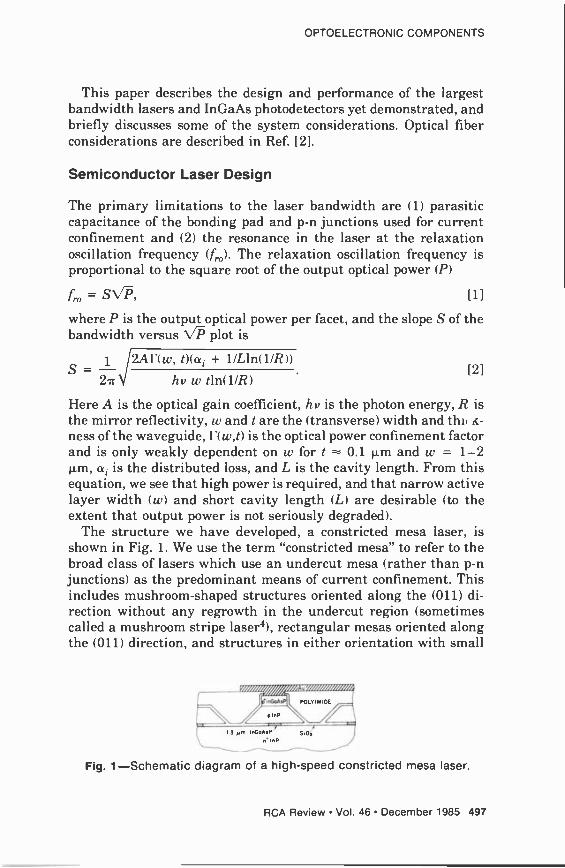
OPTOELECTRONIC COMPONENTS
This paper describes the design and performance of the largest bandwidth lasers and InGaAs photodetectors yet demonstrated, and briefly discusses some of the system considerations. Optical fiber considerations are described in Ref. 121.
Semiconductor Laser Design
The primary limitations to the laser bandwidth are (1) parasitic capacitance of the bonding pad and p -n junctions used for current confinement and (2) the resonance in the laser at the relaxation oscillation frequency (fro). The relaxation oscillation frequency is proportional to the square root of the output optical power (P)
fro =SY, 111
where P is the output optical power per facet, and the slope S of the bandwidth versus VP plot is
1 /2A1'(w, t)(a; + 1/Lln(1/R)) S =
2.r\ by w tln(1/R) [2]
Here A is the optical gain coefficient, by is the photon energy, R is the mirror reflectivity, w and t are the (transverse) width and this &-
ness of the waveguide, l'(w,t) is the optical power confinement factor and is only weakly dependent on w for t = 0.1 p.m and w = 1-2 µm, a; is the distributed loss, and L is the cavity length. From this equation, we see that high power is required, and that narrow active layer width (w) and short cavity length (L) are desirable (to the extent that output power is not seriously degraded).
The structure we have developed, a constricted mesa laser, is shown in Fig. 1. We use the term "constricted mesa" to refer to the broad class of lasers which use an undercut mesa (rather than p -n junctions) as the predominant means of current confinement. This includes mushroom -shaped structures oriented along the (011) di- rection without any regrowth in the undercut region (sometimes called a mushroom stripe laser4), rectangular mesas oriented along the (011) direction, and structures in either orientation with small
//amIviiiiaaoiiiia. POIYIMIDE
Fig. 1-Schematic diagram of a high-speed constricted mesa laser.
RCA Review Vol. 46 December 1985 497

amounts of vapor -phase epitaxial (VPE) regrowth (VPTS or VPR6 lasers), metal -organic chemical -vapor -deposited regrowth,7 mass - transported regrowth (mass -transport laser8), or liquid-phase-epi- taxial (LPE) regrowth.
LPE is used to grow the base structure, which consists of a highly doped n+ substrate, an active layer of 1.3 -11m -wavelength InGaAsP, a highly doped p+ InP layer, and a highly doped p+ InGaAsP layer to reduce the contact resistance. The undercut mesa is formed by a combination of wet and dry etching steps, and a small amount of VPE regrowth along the sides of the mesa is used to decrease optical scattering and decrease the nonradiative recombination at the edge of the active layer. The mesa is coated with chemically vapor deposited SiO2, and a thick (1.2 p.m) layer of polyimide is used to reduce the bonding -pad capacitance. Ohmic contacts are made to the p and n sides, and the wafer is cleaved into chips.
The resistance of the laser is inversely proportional to its length (L), and is typically 411 for a 250 -µm -long laser. The parasitic ca- pacitance has three components, all of which are proportional to the cavity length: the bonding pad capacitance (0.33 pF for L = 250 p.m), the mesa capacitance (0.27 pF for L = 250 p.m), and the voltage -dependent capacitance of the p -n homojunction in the VPE regrown layer. The total capacitance of a 250 -p.m -long laser is typ- ically 0.8 pF, resulting in a parasitic roll -off frequency of (2irRC)-1 = 50 GHz.
The laser is connected directly to a 46-GHz-bandwidth Wiltron K connector to microstrip adapter by a short (0.2 mm) Au wire. The bond wire inductance is <0.3 nH.
Semiconductor Laser Performance
We have demonstrated laser thresholds as low as 11 mA at 23°C for a 250 -µm -long laser. The median threshold is typically 25 mA, and the quantum efficiency is typically 0.15 mW/mA/facet. A typical light -power -versus -current curve is shown in Fig. 2. Peak pulsed powers of 40 mW are typical, while peak cw powers are lower, typ- ically 10-15 mW/facet. The polyimide layer, which helps give this structure its low capacitance, also increases the thermal resistance and lowers the peak cw power.
The small -signal frequency response and impedance of the lasers are measured with an HP 8510 network analyzer (Fig. 3) and a 36- GHz bandwidth photodiode.3 An optical isolator is inserted between the laser and detector to minimize optical feedback, which causes small ripples in the frequency response. Fig. 4 (top) shows cw fre-
498 RCA Review Vol. 46 December 1985

OPTOELECTRONIC COMPONENTS
200 CURRENT (mA)
300
Fig. 2-Light-current relationship for a typical constricted -mesa laser.
quency responses at 20°C. The response is flat up to the region of the relaxation oscillation frequency, and then a resonance occurs with a roll -off above the resonance of 40 dB/decade (plus any roil - off due to parasitic elements). As the current (and optical power)
HP8510 NETWORK ANALYZER
It 45MHZ TO 26.5GHZ
S -PARAMETER TEST SET
LASER LENS
.m__o dc BIAS
36 GHZ
In GO As PHOTODETECTOR
Fig. 3-Experimental arrangement for measuring frequency re- sponses.
OPTICAL ISOLATOR
BEAM SPLITTER
RCA Review Vol. 46 December 1985 499

20.0
10.0
0.0
-10.0
-20.0 00
20.0
10.0
0.0
- 10.0
- 20 0 0
I . I i , 1
5.0 10.0 15.0 20.0
FREQUENCY [GHz]
Cw -60°C
9mA
iiii./iAM%iiiiiii
WAY' OLYIMIDE
VPE InPgi02 1.3µmInGOASP 41. 2CmA n+ InP
40m140mA .. -I.r,
5 10 15
=REQUENCY [GHZ
20 25
Fig. 4-Small-signal cw frequency responses at several do bias currents for heatsink temperatures of 20°C (top) and -60°C (bottom).
500 RCA Review Vol. 46 December 1985

OPTOELECTRONIC COMPONENTS
increase, the resonance shifts to higher frequencies and the height of the resonance peak decreases approximately inversely propor- tional to optical power. As the laser is cooled, the laser threshold decreases; the quantum efficiency, peak power, and optical gain coefficient increase; and higher frequency operation is possible. Fig. 4 (bottom) shows the response at - 60°C where the maximum band- width is 26.5 GHz.
The dependence of 3 -dB bandwidth on the square root of optical power is shown in Fíg. 5, where we see a linear dependence on 131/2
in agreement with Eq. 111. The increasing slope at lower tempera- tures is a reflection of a larger gain coefficient. The frequency re- sponse of the laser to a 200-ns dc and rf pulse is also shown in Fig. 5 where we see a linear dependence up to the pulsed measurement limit of 22 GHz. This indicates that our present bandwidth limita- tions are predominately thermal.
The above discussion has described the small -signal modulation characteristics of the laser. We see that the modulation character- istics are strongly dependent on the dc bias current, indicating that the large -signal modulation characteristics are complicated. In par -
30
20
10
TEMPERATURE SLOPE °C (OHZ/mw)
- -60(CW) 8.7 - -30(CW) 8.3
20(CW) 5.3 20 (PULSED) 6.2
-60°C
20°C
CW MEASUREMENT LIMIT
PULSED MEASUREMENT LIMIT
i i , 1 , i , i , 1 1 , , , , . , i . .
1 1 , i
4 2
POWER 1/2 mw v2 3
Fig. 5-Power dependence of the 3 -dB bandwidth for a constricted mesa laser showing the effects of different temperatures and cw (solid lines) or pulsed (dashed line) conditions.
RCA Review Vol. 46 December 1985 501

ticular, we expect fast response when both the on and off levels are far above threshold, and the relaxation oscillation frequency is al-
ways high. When the off level is near or below threshold, the re-
sponse is more complicated. Fig. 6 shows the laser response to ex-
tremely fast nonreturn-to-zero (NRZ) pseudorandom modulation at 8 Gb/s. Gnauck9 obtained the driver signal (Fig. 6, top) by taking the pseudorandom NRZ 2-Gb/s signal from an Anritsu word gen-
erator, splitting into two signals, delaying one signal, recombining in a 2 x 1 multiplexer to obtain a 4-Gb/s signal, and then repeating the process again to get 8 Gb/s. Fig. 6 (center) shows the signal after modulating the intensity of a constricted mesa laser and then de-
tecting with a PIN detector (described below). The laser was biased at threshold, which causes some pattern effect, primarily in ringing during multiple "ones". Nonetheless, the laser rise and fall times are under 100 ps. The eye diagram (Fig. 6, bottom) shows some eye closure due to pattern effects and additional noise.
In related large -signal modulation experiments, we have gain - switched constricted mesa lasers using cw sinewaves and dc -biasing
DRIVER FIXED PATTERN
ZERO LIGHT - RECEIVED OPTICAL FIXED PATTERN
I , , I
lap ZERO .
LIGHT
4
- RECEIVED SU- E YE DIAGRAM i
Fig. 6-(Top) Fixed pattern current drive, (middle) fixed pattern received signal, and (bottom) received signal eye diagram for 8-Gb/s mod- ulation at 15°C. The optical signal was detected with a 22-GHz
detector amplified with a 7-GHz B & H amplifier and displayed on
a Tektronix oscilloscope with an S-4 sampling head.
502 RCA Review Vol. 46 December 1985

OPTOELECTRONIC COMPONENTS
the laser slightly below threshold. 100% optical modulation was achieved at frequencies up to 14 GHz. Lin and Bowers10 have com- bined pulses from a comb generator to simulate 16-Gb/s NRZ fixed codes and found that the constricted mesa laser output accurately reproduced the original modulation signal when the do bias was twice threshold.
PIN Detector Design
A number of high-speed photodetectors have been demonstrated using PIN11-16 and Schottky diode17-19 structures. Most of the long - wavelength detectors use a back -illuminated punch -through design demonstrated by Lee et al.11
To obtain the maximum bandwidth of a PIN detector, the transit time and parasitic capacitance limitations must be addressed. To minimize the transit time, thinner intrinsic layers are suggested, but to minimize the inherent parasitic capacitance of the detector junction, thicker intrinsic layers are desirable. Consequently, for any given detector junction area, there is an optimum intrinsic - layer thickness that gives the maximum bandwidth. This tradeoff is shown in Fig. 7 where the -3 -dB bandwidths of PIN detectors of different radii are shown. The calculation assumes the roll -off is due to (1) a current source driving at a parallel combination of the inherent PIN capacitance (C = 0.038'L pF µm corresponding to a 10 -11m -radius detector) and a 5052 load resistance and (2) a transit time limitation given by
1(u') 1 e-jwr-aL 1+ Q -J' 7 n - 1 1 - !(o) (1 - e-) -JWT - aL JWT JWTp
1
aL - jWTp
where r is the detected current, co is the angular modulation fre- quency, a is the absorption length, L is the absorbing layer thick- ness, T(=L/v) and Tp(= L/up) are the electron and hole transit times, respectively, up and u are the hole and electron veloci- ties, respectively, and an ewÍ time dependence is assumed (not as in Ref. 131). This relation assumes a saturated velocity, ignores the phase change of the light as it traverses the absorbing layer (valid since u,vp<c), and assumes the absorbing -layer thickness is equal to the depleted high -field intrinsic -layer thickness. There is an ad- ditional current term due to the diffusion of carriers from the low - field region,21 and it can be significant at low frequencies for very
131
RCA Review Vol. 46 December 1985 503

2 o I o o z
100.0
75.0
50.0
25.0
TRANSIT TIME LIMIT
_- 1.0
-J0.8_1 a r.
Au/Zn CONTACT p' InGaAs - n' InGaAs - 0.6 z n' InP W
LL,
W
Au/Sn W
/ 10 CONTACT - 0.4 p 1 U W
10 -J -J 0
0.2
/ 2
50 100
LIGHT
0.0 1 , , r r , t II ti 1 0.0 0 0 1.0 2.0 3.0 4.0
INTRINSIC LAYER THICKNESS {µm]
Fig. 7-Dependence of 3 -dB bandwidth on absorbing -layer thickness for several detector radii. The dashed curve shows the prediction for a 10 -11m -radius detector with 0.05-pF stray capacitance included. The dotted line shows the dependence of collection efficiency (1-a-"'-) on the absorbing layer thickness L. These curves assume v = 7 x 106 cm, vp = 6.5 x 106 cm, a = 1.151.1m-1 corresponding to an incident wavelength of 1.3 p.m.
5 0
high speed devices which have (íL41. For front -side illumination, Eq. ]3] is valid if the subscripts p and n are switched.
We see from Fig. 7 that bandwidths of 75 GHz or higher are possible, provided thin absorbing layers and small detector areas are used. The problem with this approach is the decreased quantum efficiency of the very thin layer detectors (dashed line in Fig. 7).
PIN Detector Performance
High-speed photodetectors can be characterized using the system shown in Fig. 8. A comb of short pulses at a repetition rate % in the time domain is equivalent to a comb of frequencies spaced by /o, in the frequency domain. Provided the optical pulses are sufficiently short (Fig. 9), any roll -off measured on a spectrum analyzer is due to the response of the photodetector. A typical measurement is shown in Fig. 10 for a PIN InGaAs photodetector with an intrinsic -
504 RCA Review Vol. 46 December 1985

OPTOELECTRONIC COMPONENTS
AUTO CORRELATOR
/8Ops
YAG LASER PULSE
X= 1.06 µm COMPRESSOR
100 MHZ
r . 3ps
L ENS
HP8566 SPECTRUM ANALYZER .
dc _ BIAS
PHOTO - DETECTOR
Fig. 8-Experimental arrangement for measuring detector frequency re-
sponse.
layer thickness of 1.5 µm and a radius of 12 p.m. Recently, Bowers,
Burrus, and McCoy3 used thin (0.5-µm) intrinsic layers and a small
detector radius (7 µm) to demonstrate bandwidths of 36 GHz. Fig.
11 shows the measured and calculated frequency response of this
1000
100
10
0.1
1 t t 1 1 I 11 I I 1 , 1 1 t t l 1-1-_1_1-11 .. 1.0 10 100
PULSE WIDTH(FWHM1nS
Fig. 9-Dependence of 3 -dB (electrical) bandwidth of a detected optical pulse train on FWHM of the optical pulse (assuming a hyperbolic
secant amplitude dependence). Ideally, the FWHM is short enough so that the 3 -dB frequency of the pulse train is beyond
the measurement range.
RCA Review Vol. 46 December 1985 505

...,. ..
1000:1 DUTY CYCLE 10 V BIAS
_ a'
y(lPJlllll J iIIW aii W111 1411 ,ílllüi I1II 1Wi1114
1111 I NUN 111113111111111
I! _AqllBlllizliz[1i1j .. iww.w .w.w rr 2
FREQUENCY(GHz) 92
Fig. 10-Frequency response of an InGaAs photodetector with a 1.5 -µm - thick absorbing layer for excitation with 10-mW peak power 10- ps FWHM pulses at a 100 -MHz rate.
m 17 ", J
....
Z C) 00 d J tn 0 W N CC
20.0
10.0
O.0
- 10.0
SOLID CURVES
- 20.0 ' ' ' 0.0
1 I
10.0
0.3 nH IL
5012
1 I 1
20.0 FREQUENCY [GHz]
30.0 40.0
Fig. 11- Frequency response of back -illuminated PIN photodetectors. The dashed lines show the transit -time limited response (Eq. [1] with values given in the text), while the solid lines show the response with both transit -time and parasitic effects (see inset) included.
506 RCA Review Vol. 46 December 1985
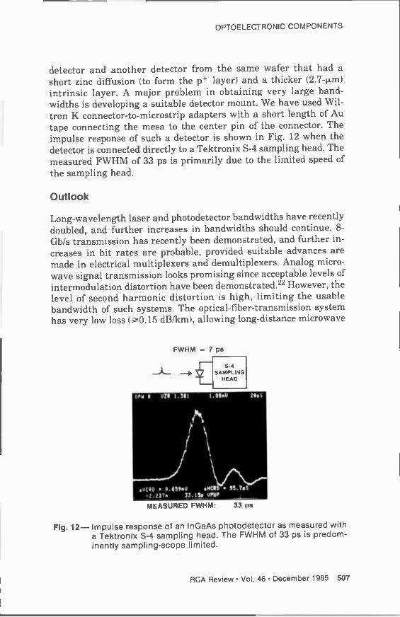
OPTOELECTRONIC COMPONENTS
detector and another detector from the same wafer that had a
short zinc diffusion (to form the p+ layer) and a thicker (2.7-µm) intrinsic layer. A major problem in obtaining very large band- widths is developing a suitable detector mount. We have used Wil-
tron K connector-to-microstrip adapters with a short length of Au
tape connecting the mesa to the center pin of the connector. The impulse response of such a detector is shown in Fig. 12 when the detector is connected directly to a Tektronix S-4 sampling head. The measured FWHM of 33 ps is primarily due to the limited speed of
the sampling head.
Outlook
Long -wavelength laser and photodetector bandwidths have recently doubled, and further increases in bandwidths should continue. 8-
Gb/s transmission has recently been demonstrated, and further in-
creases in bit rates are probable, provided suitable advances are made in electrical multiplexers and demultiplexers. Analog micro-
wave signal transmission looks promising since acceptable levels of
intermodulation distortion have been demonstrated.22 However, the level of second harmonic distortion is high, limiting the usable bandwidth of such systems. The optical -fiber -transmission system has very low loss (;0.15 dB/km), allowing long-distance microwave
FWHM = 7 ps
_ --- S-4
SAMPLING HEAD
orlY e U211-1.311 1.88aU 2l05
UCCD 9.01a1.1 NC*D 93.1 5
2.217 11.4, MP -
MEASURED FWHM: 33 ps
Fig. 12- Impulse response of an InGaAs photodetector as measured with a Tektronix S-4 sampling head. The FWHM of 33 ps is predom- inantly sampling -scope limited.
RCA Review Vol. 46 December 1985 507

transmission. However, the conversion loss from electrical -to -op- tical -to -electrical signals is significant (>20 dB), and this elimi- nates some applications. Nonetheless, optical transmission systems presently exist with bandwidths covering many waveguide bands. Furthermore there are a number of fiber -optical components, such as directional couplers, that have significantly better performance (such as directivity and bandwidth) than their microwave counter- parts, and new applications will surely be demonstrated.
Acknowledgments
The authors wish to thank T. J. Bridges, E. G. Burkhardt, A. H. Gnauck, B. R. Hemenway, J. P. Heritage, C. Lin, R. J. McCoy, J. M. Wiesenfeld, and D. P. Wilt for many useful contributions to this work.
References:
'J. E. Bowers, B. R. Hemenway, D. P. Wilt, T. J. Bridges, and E. G. Burkhardt, "26.5- GHz-Bandwidth InGaAsP Constricted Mesa Lasers with Tight Optical Confine- ment," Electron Lett., 21, p. 1090 (1985). 2 K. Ogawa, "Considerations for Single -Mode Fiber Systems," Bell System Tech. J., 61, p. 1919 (1985). 3 J. E. Bowers, C. A. Burrus, and R. J. McCoy, "InGaAs PIN Photodiodes with Mod- ulation Responses to Millimeter Wavelengths," Electron Lett., 21, p. 812 (1985). 4 H. Burkhard and E. Kuphal, "Three -and -Four -Layer LPE InGaAs(P) Mushroom Stripe Lasers for J1 = 1.30, 1.54, and 1.66 µm," J. Quantum Electron., QE -21, p. 650 (1985). 5 T. L. Koch, L. A. Coldren, T. J. Bridges, E. G. Burkhardt, P. J. Corvini, and B. I. Miller, "Low -Threshold High Speed 1.55 µm Vapor Phase Transported Buried Het- erostructure Lasers (VPTBH)," Electron Lett., 20, p. 856 (1984). 6 C. B. Su, V. Lanzisera, W. Powazinik, E. Meland, R. Olshansky and R. B. Lauer, "12.5-GHz Direct Modulation Bandwidth of Vapor Phase Regrown 1.3-µrn InGaAsP Buried Heterostructure Lasers," Appl. Phys. Lett., 46, p. 344 (1985). 7 U. Koren, private communication. 8 Z. L. Liau and J. N. Walpole, "A Novel Technique for GalnASP/InP Buried Het- erostructure Laser Fabrication," Appl. Phys. Lett., 40, p. 568 (1982). 9 A. Gnauck, private communication. i0 C. Lin and J. E. Bowers, "High Speed Large Signal Digital Modulation of a 1.3 µm InGaAsP Constricted Mesa Laser at a Simulated Bit Rate of 16 Gb/s," submitted to Electron. Lett., 21, p. 906 (1985). 11 T. P. Lee, C. A. Burrus, K. Ogawa, and A. G. Dentai, "Very High Speed Back - Illuminated InGaAs PIN Punch Through Photodiodes," Electron. Lett., 17, p. 431 (1981). 12 C. A. Burrus, J. E. Bowers, and R. S. Tucker, "Improved Very -High -Speed Pack- aged InGaAs PIN Punch -Through Photodiode," Electron. Lett., 21, p. 262 (1985). 13 J. Schlafer, C. B. Su, W. Powazinik and R. B. Lauer, "20 GHz Bandwidth InGaAs Photodetector for Long -Wavelength Microwave Optical Links," Electron. Lett., 21, p. 469 (1985). 14 K. Li, E. Rezek, and H. D. Law, "InGaAs PIN Photodiode Fabricated on Semi - Insulating InP Substrate for Monolithic Integration," Electron. Lett., 20, p. 196 (1984).
508 RCA Review Vol. 46 December 1985

OPTOELECTRONIC COMPONENTS
15 J. C. Campbell, A. G. Dentai, G. J. Ana, J. Long, and V. G. Riggs, "Planar InGaAs
PIN Photodiode with a Semi -insulating InP Cap Layer," Electron. Lett., 21, p. 447
(1985). 16 N. Bar -Chaim, K. Y. Lau, I. Ury, and A. Yariv, Appl. Phys. Lett., 43, p. 261 (1983).
17 S. Y. Wang and D. M. Bloom, "20 GHz Bandwidth GaAs Photodiode," Electron. Lett., 21, p. 262 (1985). 18 S. Y. Wang and D. M. Bloom, "100 GHz Bandwidth Planar GaAs Schottky Photo - diode," Electron. Lett., 19, p. 554 (1983). 19 N. Emeis, H. Schumacher, and H. Beneking, "High Speed GalnAs Schottky Pho-
todetector," Electron Lett., 21, p. 180 (1985). 20 S. M. Sze, Physics of Semiconductor Devices, 2nd edition, John Wiley & Sons, New York, 1981, p. 756. 21 T. H. Windhorn, L. W. Cook, and G. E. Stillman, "Temperature Dependent Elec-
tron Velocity Field Characteristics for In053Ga0.47As at High Electronic Fields," J.
Electron. Mat. 11, p. 1065 (1982). 22 T. E. Darcie, R. S. Tucker and G. J. Sullivan, "Intermodulation and Harmonic Dis-
tortion in InGaAsP Lasers," Electron. Lett., 21, p. 665 (1985).
RCA Review Vol. 46 December 1985 509

Microwave Hyperthermia and Radiometry: One -Dimensional Computer Models
Morris Ettenberg City College of New York, New York, NY 10031 Consultant, RCA Laboratories, Princeton, NJ 08540
Abstract-Several computer programs based on the Bio-Heat Equation have been written to model the effect of microwave radiation on a biological body. For the hyperthermia model, the body is irradiated by an external microwave Dower source and the steady-state temperature distribution is calculated and dis- played graphically. There may also be internal heat sources. The time -dependent temperature may be calculated for an abrupt change in microwave power. For the radiometry model, the microwave power source is replaced by a receiving an- tenna; the black -body radiation is calculated and converted into an apparent body temperature.
1. The Equations 1.1. The Bio-Heat Equation
The bio-heat equation' is the usual equation for heat conduction including terms for internal heat loss and generation which are spe- cialized to biological models.
aT I,C -t =V(KVT) -Qb+Q,,, 111
The meaning of the variables and their units are given in Table 1. For the steady-state case in one dimension the bio-heat equation
reduces to
a(aT1 K- -Qb+Qm = 0 r3x ix 121
510 RCA Review Vol. 46 December 1985

MICROWAVE HYPERTHERMIA
Table 1-Variables Used in Model
T Temperature °C
p Density kg/m3 C Heat Capacity J (kg °CI
K Heat Conductivity \V Im °C1
t Time s Qr, Heat Loss W'm3 Q,,, Heat Generation W m3
In the hio-heat equation the heat loss term, Qb, represents the
regulation of the tissue temperature by the arterial blood flow and
is given by
Qb = r1PpC(T - To) 131
where To is the arterial blood temperature, >1 is a dimensionless
efficiency constant, and P is the blood perfusion rate in 1/s.
While the Qb term contributes to cooling the tissue when the tissue temperature is higher than the arterial temperature, it heats
the tissue when the tissue temperature drops below the arterial temperature. The perfusion rate, P, describes the vascularization of the tissue, or how well the tissue is supplied with blood vessels and,
in effect, how rapidly the blood is moving. The efficiency factor, r1,
describes how well the tissue is coupled to the local vascular system. In our model. we consider the product, TIPpC, as the blood -
flow rate, for which measured data are available. Although the blood -flow rate is given in the medical literature in units of milli- liters(minute 100 grams)-', it should be noted that milliliters here refers to mass, presumably that of water as a reference, and
not to volume. We may note further that all the units are reduced to
MKS in the computer programs. The heat generation term, Q,,,, may be derived from the micro-
wave power propagated through a body with attenuation con-
stant a:
P = Poexp( - 2ax)
The power lost per unit length will be
aP - 2aPoexp( - 2ax) = - 2aP ax
Therefore, the power required to heat a length, dx, at a distance, x,
from the plane where the power is P0 will be
Q,,, = 2aPdx = 2adrPoexp(- 2ax) 141
RCA Review Vol. 46 December 1985 511

In the linear one-dimensional model, all calculations are made for a unit cross-sectional area, and only power densities are considered. For the one-dimensional radial model, the incident power is con- verted to a power density at the surface of the cylindrical radiating element, and all subsequent calculations are made in terms of power density. Since the different layers of tissue have different di- electric constants, causing reflections from the interfaces, the total power contributing to the heating of a region, dx, will be the sum of the incident and the reflected powers. In addition, the program pro- vides for heating due to an internal localized heat source.
For the radiometry calculation, we use the formulae for the re- ceiving -antenna temperature, TA, due to a source at Ts seen through a medium of thickness, d, and attenuation constant, a, at T.t1:
T = TN,I 1 - exp(- 2ad)J + Tsexp(- tad) 151
1.2. Boundary Conditions
Since the model of the body is made up of several tissue layers with front (facing the microwave source) and back surfaces, we require boundary conditions at each of the interfaces.
At the front and back surfaces, the body is cooled by convection to a medium of ambient temperature, To, giving a boundary condi- tion of
1 T K-=H(T-To) ax 161
where H is the surface convection coefficient in W(me °C)-1. Within the body, the boundary condition at the interface between
adjacent layers ni and m + 1 is
aT 1 r aT K- ILK - 171
d Y má1.Y m+ 1
2. The Model 2.1. The Model
The body is modeled as a series of sections for which the physical parameters may be specified at the input and modified interactively as the program is running. For computational purposes each section is subdivided into a maximum of 20 layers at which the tempera -
512 RCA Review Vol. 46 December 1985

MICROWAVE HYPERTHERMIA
ture is calculated. The parameters used in the model are shown in Table 2, which is a copy of the file read by the program as input. We refer to Table 2 to discuss each of the model parameters (see Sec- tions 2.2 through 2.13).
2.2. Sections and Layers
The program reads NS, the number of sections, and NL, the number of layers in each section. In the example shown, we have five sec- tions with 10 layers in each section. The number of sections will be determined by the kinds of tissue in the model, but there is some choice in assigning the number of layers. The use of more layers gives higher accuracy since the finite difference algorithm ap- proaches a differential, but it takes more computing time. Partic- ular cases may require some experimentation to find a suitable ac- curacy and speed.
2.3. Tissue
There are four types of tissue recognized by the program: skin, fat, muscle, and bone. When a section is specified as one of these types, the physical parameters shown in the bottom half of Table 2 are assigned. The program reads only through the line labeled IMCH IEPS etc. (parameters explained in Section 2.13). The remaining lines are for reference, showing the assigned values. These values may be changed interactively when the program is run. They cannot be changed in the input file.
In addition to assigning these physical parameters, the program also assigns a complex dielectric constant to each type of tissue, depending on the frequency and the water content. The dielectric constant is found from a formula derived by a ninth -order regres- sion from a table3 of measured values. A comparison of the mea- sured data and the formula values is given in Table 3. The dielec- tric constant may also be changed interactively while the program is running.
2.4. Condition
The program recognizes NORMAL and TUMOR as tissue condi- tions. In the NORMAL condition the blood flow increases with tem- perature. In the TUMOR condition the blood flow increases with temperature up to a maximum at a given critical temperature and
RCA Review Vol. 46 December 1985 513

Tab
le 2
-Phy
sica
l Pa
ram
eter
s U
sed
in t
he M
odel
5 10
10
10
10
10
N
S, N
L
SKIN
FA
T
MU
SCL
E
MU
SCL
E
MU
SCL
E
TIS
SUE
N
OR
MA
L
NO
RM
AL
N
OR
MA
L
TU
MO
R
NO
RM
AL
C
ON
DIT
ION
0.
2 0.
5 1.
0 1.
5 2.
8 D
(cm
)
0.
0.
0.
0.
0.
Q(i
iit)
1.
1.
1.
1.
1.
EPS
(rea
l ) 0,
0.
0.
0.
0.
E
PS(i
mag
) 5.
E3
1.E
-
4 1.
5 IT
h1A
X E
RR
MA
X F
OY
ER
0.
2 0.
4 0.
2 -0
.4
FN1
FN2
FT1
FT2
1.
0.
50.4
8 32
.0
EPS
(fro
nt)
EPS
(bac
k)
14.6
5 60
. 27
. 37
. H
F H
B T
OF
TO
B
37.
39.5
1.
T
A T
CR
IT F
C1
915.
10
0.
FRE
Q(M
Hz)
P0(
mW
/cm
2)
Y
N
Y
Y
IMC
H I
EPS
IG
RF
IME
N
Para
met
er V
alue
s A
ssig
ned
to T
issu
e T
ypes
SKIN
FA
T
MU
SCL
E
BO
NE
T
issu
e H
IGH
L
OW
H
IGH
L
OW
W
ater
Con
tent
H
eat
Con
duct
ivity
Im
W(c
m
°C)
'1
Hea
t C
apac
ity I
cal(
g °C
)-' 1
Den
sity
(g/
ml)
B
lood
Flo
w I
ml(
min
10
0 g)
-'I
4.4.
2 2.
10
6.42
14
.60
0.75
0.
54
0.83
0.
30
1.20
0.
937
1.10
1.
79
12.8
0 1.
50
2.70
0.
50

MICROWAVE HYPERTHERMIA
Table 3-A Comparison of Measured and Calculated Dielectric Constants
A. Tissue with
Frequency (MHz)
Low Water Content (Fat, Bone) Dielectric Constant Conductivity (Sim)
Measured Calculated Measured Calculated
27 20.0 19.8 0.027 0.027 41 14.6 14.8 0.033 0.034
100 7.45 7.85 0.047 0.047 200 5.95 5.76 0.060 0.059 300 5.7 5.4 0.069 0.068 433 5.6 5.4 0.078 0.078 750 5.6 5.7 0.094 0.095 915 5.6 5.7 0.101 0.102
1500 5.6 5.8 0.121 0.123 2450 5.5 5.6 0.155 0.152 3000 5.5 5.5 0.172 0.169 5000 5.5 5.2 0.236 0.235 5800 5.05 5.1 0.262 0.263 8000 4.7 4.8 0.343 0.348
10000 4.5 4.5 0.437 0.433
B. Tissue with
Frequency (MHz)
High Water Content (Muscle. Skin) Dielectric Constant Conductivity (Sim)
Measured Calculated Measured Calculated
27 113. 113. 0.612 0.623 41 97.3 97.2 0.693 0.676
100 71.7 70.5 0.889 0.924 200 56.5 58.4 1.28 1.20 300 54. 54. 1.39 1.36 433 53. 52. 1.43 1.48 750 52. 51. 1.54 1.60 915 51. 50. 1.60 1.62
1500 49. 50. 1.77 1.72 2450 47. 48. 2.21 2.04 3000 46. 47. 2.26 2.34 5000 44. 43. 3.92 3.98 5800 43. 42. 4.73 4.81 8000 40. 41. 7.65 7.52
10000 39.9 40.0 10.3 10.3
then decreases to a minimum value. The equations that model the blood flow are
BF = BFo11 + at + a)tanh b(T - Tc)]
BF = BF011 + at + (a2 - at)tanh /AT - Tc)]
for T<T, 181
for T > T, 191
For this model of blood -flow variation with temperature, the ratio of BF/BF0 is near 1 for T < T, rises to 1 + at for T = T, and ap- proaches 1 + a2 for T > Te.
For the NORMAL condition,
al = FN1 and a2 = FN2 1101
RCA Review Vol. 46 December 1985 515

For the TUMOR condition,
a, = FT1 and a2 = FT2
For both conditions,
b = FC1 and T, = TCRIT
2.5. Thickness: D(cm)
1121
In the input file line labeled D(cm), the thickness of each section of tissue is specified in centimeters. The example shown in Table 2 is seen to be a model of the following five sections:
(1) 0.2 cm of normal skin (2) 0.5 cm of normal fat (3) 1.0 cm of normal muscle (4) 1.5 cm of tumor muscle (5) 2.8 cm of normal muscle
2.6. Internal Heat Source: Q(int)
The input values assigned on this line allow for modeling a fevered tissue since there are cases where a tissue layer, without external power input, may have a temperature higher than that of the arte- rial blood. To simulate a fever of two or three degrees (Celsius), the required Q(int) will be approximately 10 or 20.
2.7. Complex Dielectric Constant: EPS(real), EPS(imag)
Instead of using the assigned values of the complex dielectric con- stant, which depend on frequency and tissue, one may assign arbi- trary values of the real and imaginary parts on these two lines. To have these assigned values used, the value of IEPS must be Y. The same effect may be achieved while the program is running by an- swering YES to the question of assigning arbitrary values to the dielectric constant. In the program the complex dielectric constant is in the form of
E = E,. - ,JE¡
where
1131
E,. = EPS(real) and E! = EPS(imag) 1141
2.8. Computational Variables: ITMAX, ERRMAX, FOVER
The value assigned to ITMAX determines the maximum number of
516 RCA Review Vol. 46 December 1985

MICROWAVE HYPERTHERMIA
iterations allowed for convergence of the calculated temperature to a value that changes less than ERRMAX in the last iteration. If the iteration does not converge, the program announces this condition and permits changing the values of ITMAX and ERRMAX without quitting the program. Lack of convergence may be caused by taking too few layers per section. The variable FOVER allows for overre- laxation in order to reduce the number of iterations required for convergence.
2.9. Condition Factors: FN1, FN2, FT1, FT2
The variation of blood flow with temperature is determined by FN1 and FN2 for the NORMAL condition and by FT1 and FT2 for the TUMOR condition. While FN1 and FT1 apply below the critical temperature, FN2 and FT2 apply above the critical temperature. From Table 2 we see that it is the negative value of FT2 which models the decrease in blood flow in the TUMOR condition. This variation is the only change made by the program for the TUMOR condition. If there are other parameters to be modeled, the changes must be made interactively.
2.10. Surrounding Media
The medium in front of the body, i.e., the region containing the mi- crowave power source, is specified by its complex dielectric con- stant, EPS(front), its convection coefficient, HF, and its tempera- ture, TOF. Corresponding quantities for the back surface are EPS(back). HB, and TOB.
We see from the input values in Table 2 that this model has the front medium as air (e = 1 - j0) at room temperature (T = 27°C) with a convection coefficient of 14.65, which is characteristic of the interface between skin and calm air. The back surface is muscle (e = 50.48 - j32.00)* at normal body temperature (T = 37°C) with a high convection coefficient that will hold the temperature at that surface close to the normal body temperature.
This model is seen to be the first 6 cm of a thicker body character- ized as muscle at normal body temperature.
2.11. Arterial and Critical Temperatures
The normal body temperature is taken as the arterial blood temper-
' These values were found by running the program.
RCA Review Vol. 46 December 1985 517

ature, TA; the critical temperature and the slope factor used in cal- culating blood flow are TCRIT and FC1. The formulas used in mod- eling blood flow are given in the section on blood flow (see Sec- tion 2.4).
2.12. Microwave Frequency and Power Density
From Table 2 we may see that the model is being irradiated by a microwave power source at a frequency of 915 MHz and a power density of 100 mW/cm2.
2.13. Run Control Variables
The last line of input data read by the program specifies the starting conditions as follows:
IMCH specifies that the microwave power source is matched to the front surface of the model body when its value is specified as Y
(for YES). In this case the actual power source is unspecified, but the power density transmitted through the front surface is PO. If the value of IMCH is given as N (for NO), the power density of the source is PO and the reflection and transmission coefficients are cal- culated at the front surface; then, only the transmitted power is used to calculate tissue heating.
IEPS specifies that when its value is Y, the arbitrary values of the dielectric constant given in the input data file shall be used. When the value of IEPS is N, as in Table 2, arbitrary values are not used; the program then calculates the dielectric constant as a func- tion of frequency for different types of tissue.
IGRF specifies that the temperature shall be plotted when the value of IGRF is Y. Otherwise, an abbreviated printed output is presented on the screen. This is much faster than using graphical output and is useful for preliminary exploratory models.
IMEN specifies the "short" menu for the program interaction when the value of IMEN is Y. The "long" menu is recommended for anyone learning to run the program. There is no on-line instruc- tion, but the long menu is intended to be self-explanatory.
3. The Algorithms 3.1. The Algorithms
To solve the bio-heat equation it is converted to a finite difference equation for a finite one-dimensional spatial net. For the steady state the equation is a nonlinear Poisson equation that converges
518 RCA Review Vol. 46 December 1985

MICROWAVE HYPERTHERMIA
from any assumed solution, at least for the nonlinearities generally used in this model. The transient solution starts from the tempera- ture distribution found for the steady state and then calculates the increment in temperature for each time increment when the micro- wave power density is varied in time. In this model the only time variation permitted is that of power density.
3.2. The Steady -State Solution
The steady-state solution proceeds as follows: (1) The initial temperature assigned to each point of the body is
the arterial blood temperature, T. (2) Starting from the front and taking each point in turn until
the back is reached, one recalculates the temperature according to the position of the point. Calculations for various portions are shown below.
(a) Front and Back Surfaces. The temperature here is calculated from the boundary condition (see Eq. [61 in Section 1.2). Reduced to finite differences, the temperature at the front surface is given by
H T-` +-1rTo
K T -
H -1r + 1 K
1151
and the temperature at the back surface, by
H T- + -1r To
K T -
H 1161
- 1r + 1 K
where T+ refers to the next point of larger x and T- refers to the next point of smaller x.
(b) Boundary Between Internal Sections. The temperature at the boundary point between the internal sections in and in + 1 is cal- culated from Eq. 171, which reduces to
[K 11' TJ,n +
[ T T- JPt, +I
l ` 1iJm + [jm+i
1171
RCA Review Vol. 46 December 1985 519
where T on the right-hand side refers to the nearest point in the different sections.
(c) Internal Point. If the point is not on any boundary then it must satisfy the bio-heat equation, Eq. 111, which reduces to
1 (1v)2 (102 T=2 T++T-- Qb + Q, 118]
where T-1- and T- are the temperatures at the nearest neighboring points.
Since Qb depends on the blood flow, which in turn depends on the temperature, we replace Qb by using Eq. 131 in the form
Qb = V3T 1191
where T has replaced T - T and where Vs = BF includes the variation of blood flow with temperature, and then solve for T
Z [T+ (')1 - + T- +
T - 1 (1v)2 120j
1 + V. 2 K
The tissue heating term, Q is the sum of two terms,
Q,,,=Q++Q- where Q+ is due to the incident power density, P },
Q+ = 2a1vP+expl (- 2a(x - x1)1
and Q- is due to the reflected power density, P-, Q- = 2a1xP-expl +2a(x - xr)1
1211
1221
123]
where xf is the first point in the section and x1 is the last point and
P- = Jl'J2P+exp(-2ad) 1241
where d is the width of the section and a is the attenuation con- stant.
At the boundary between the sections n - 1 and n the reflection and transmission coefficients, r _ , and 7, are given by
1 - i - 1
\
in -1) 1'eXp( - 2yd ) E-1 - \ 1251
1 + in -1 (1 vl -1 I exp(- 2Yd, )
Tin ` 1I J
520 RCA Review Vol. 46 December 1985

MICROWAVE HYPERTHERMIA
2
+ Tin -1
I 1 Tin-1
rneXP(-2ynn) Tin 1\\ Tin /I
d
[261
where yn is the complex propagation constant in section n. We see
that the reflection and transmission coefficients are calculated from
the back to the front; then the transmitted power into each section
is calculated from the front to the back:
Pn = Pn-1(1 - Ihn-1I2)exp(-2an-idn-i) f27]
(3) The difference between the initial and the recalculated tem-
perature is calculated and the largest difference for the entire array of points is found. If the absolute value of the largest difference is
greater than the assigned value ERRMAX, the process is repeated
unless the number of repetitions exceeds ITMAX. When the abso-
lute value of the largest difference does not exceed ERRMAX, the
solution is considered to have converged and the temperature dis-
tribution is plotted or printed.
3.3 Radiometry Model
Having determined the temperature distribution in the model, we
may calculate the radiometric temperature from the noise power
received by an antenna at the plane of the signal source, the source
power having been reduced to zero. The basic formula for the noise
power, P, in a frequency band, .1f, due to a source at temperature Ts is
P = kTsAf (281
where k is Boltzmann's constant. Since the power is directly proportional to the temperature, and
all the measurements are relative rather than absolute, it is conve-
nient to consider the temperature rather than the power. Therefore, when a source at Ts is seen through a lossy medium of thickness d and attenuation constant a, we shall consider the temperature to
have been attenuated; the temperature measured at the receiving antenna due to the source is given by
Tsexp(- 2ad) [291
With the medium at a temperature TM there is another contribu- tion at the receiving antenna due to the medium
TM11 - exp( - 2ad)] [301
RCA Review Vol. 46 December 1985 521

giving the antenna temperature
TA = Tsexp( - 2ad) + T,y I 1 - exp( - 2ad)]
or
TA = (Ts - TM)exp(- 2ad) + TM
1311
1321
For the sectioned model, the radiometric temperature is calculated from the medium at the back through successive sections to the me- dium at the front. If that medium is lossy, the distance from the model body to the plane of the antenna is taken into account.
3.4. The Transient Solution
The program written for the transient case allows for the following variation of microwave power density, P, with time, t:
P=Pa for t<to P=P1 for to<t<t1 P=P2 fort, <t<t2 The calculation proceeds as follows:
(1) The steady-state temperature distribution is calculated for P = Po.
(2) The temperature at each point, starting from the front and proceeding to the back, is recalculated:
(a) If the point is a boundary point, the temperature is found from the appropriate boundary condition as in the steady-state case.
(b) If the point is an interior point, the increment in temperature, .1T, for an increment in time, ,t, is calculated from Eq. 111, which reduces to
.V K = (T++T--2T)-Qr,+Q,,, 1331
pC (A.r)2
where P1 is used in calculating Q,,,. (3) The time, t, is incremented by .fit, and the temperature distri-
bution is recalculated again. (4) These steps are repeated until t = t1i and the process con-
tinues with P2 used in the calculation of Q,,, until t = t2. (5) To see the difference between the temperature reached after
the given time interval and the eventual steady-state condition, the steady-state temperature distributions are calculated for P1 and P2.
522 RCA Review Vol. 46 December 1985

MICROWAVE HYPERTHERMIA
(6) The temperature at the front surface is stored and, at the end
of the program run, is plotted versus time.
Programs Available
At this time (November 1985) the linear steady-state program is
available on the MTC HP1000/A900 as HYPLN, and the transient program as TTR.
Examples of Computer Program Output Operation
An example of the program operation for the linear simulation of
heated tissue for a depth of 6 cm is shown in Table 4. The graphical output is shown in Fig. 1. Examples of transient -solution graphs are shown in Figs. 2 and 3.
Table (-Program Operation
CI> HYPLN
Program HYPLN plots Temperature vs. Depth
DO YOU WANT TO USE THE SHORT MENU ? (Y/N):
EXTERNAL PARAMETERS
N
FREQUENCY POWER DENSITY AMBIENT TEMPERATURE -FRONT AMBIENT TEMPERATURE -BACK
915.00 100.00 27.00 37.00
MHZ mw/cm**2 DEG(C) DEG(C)
FRONT CONVECTION COEFF. 14.65 W/M**2/DEG(C)
BACK CONVECTION COEFF. 60.00 W/M**2/DEG(C)
FRONT DIEL. CONSTANT 1.00
LOSS CONSTANT 0.00
BACK DIEL. CONSTANT 50.48
LOSS CONSTANT 32.00
MODEL DATA SECT THICKNESS BLOOD FLOW
cm. ml/m/100gm TISSUE TYPE EPS1 EPS2 Q (int)
mw/cc
1 .20 12.80 SKIN NORMAL 50.48 32.00 0.00
2 .50 1.50 FAT NORMAL 5.73 2.01 0.00
3 1.00 2.70 MUSCLE NORMAL 50.48 32.00 0.00
4 1.50 2.70 MUSCLE TUMOR 50.48 32.00 0.00
5 2.80 2.70 MUSCLE NORMAL 50.48 32.00 0.00
NORMAL TISSUE FLOW PARAMETERS : .200 .200
TUMOR TISSUE FLOW PARAMETERS : .200 -.400
CRITICAL TEMPERATURE 39.500
SLOPE FACTOR 1.000
ARTERIAL TEMPERATURE 37.000 DEG(C)
TO CHANGE :
EXTERNAL PARAMETERS MODEL DATA
TO SEE CURRENT PARAMETERS TO RUN THE CURRENT MODEL
ENTER :
EXT MOD PAR RUN
RCA Review Vol. 46 December 1985 523

Table 4-Continued
TO START AGAIN START TO QUIT <CR> ? RUN
DO YOU WANT THE OUTPUT PLOTTED ? (Y/N): Y .. terminal or plotter (T/P) ? T IS THIS TO BE A NEW GRAPH ? (Y/N) Y ENTER T(min), T(max) : 30 45
TO CHANGE : ENTER :
EXTERNAL PARAMETERS EXT MODEL DATA MOD
TO SEE CURRENT PARAMETERS PAR TO RUN THE CURRENT MODEL RUN TO START AGAIN START TO QUIT <CR> ? EXT
TO CHANGE : ENTER :
POWER DENSITY POWER FREQUENCY FREQ FRONT DIEL. CONSTANT FDIEL BACK DIEL. CONSTANT BDIEL AMBIENT TEMPERATURES AMBI CONVECTION COEFFICIENTS CONV
TO CHANGE MODEL DATA MOD TO SEE CURRENT PARAMETERS PARAM TO RUN THE CURRENT MODEL RUN TO QUIT <CR> ? FREQ
FREQUENCY = 915.00 MHz TO CHANGE ENTER NEW FREQUENCY IN MHZ TO KEEP ENTER X 2450
FREQUENCY = 2450.00 MNZ TO CHANGE ENTER NEW FREQUENCY IN MHZ TO KEEP ENTER X X DO YOU WISH TO MAKE MORE CHANGES ? (Y/N) : Y
TO CHANGE : ENTER :
EXTERNAL PARAMETERS EXT MODEL DATA MOD
TO SEE CURRENT PARAMETERS PAR TO RUN THE CURRENT MODEL RUN TO START AGAIN START TO QUIT <CR> ? EXT
TO CHANGE : ENTER :
POWER DENSITY POWER FREQUENCY FREQ FRONT DIEL. CONSTANT FDIEL BACK DIEL. CONSTANT BDIEL AMBIENT TEMPERATURES AMBI CONVECTION COEFFICIENTS CONY
TO CHANGE MODEL DATA MOD TO SEE CURRENT PARAMETERS PARAM TO RUN THE CURRENT MODEL RUN TO QUIT <CR> ? POWER
524 RCA Review Vol. 46 December 1985
MICROWAVE HYPERTHERMIA
Table 4-Continued
POWER DENSITY = 100.00 mw/cm**2 (MATCHED) TO CHANGE ENTER NEW POWER DENSITY TO KEEP ENTER X : 125 IS THE POWER SOURCE MATCHED ? (Y/N) : Y
POWER DENSITY = 125.00 mw/cm**2 (MATCHED) TO CHANGE ENTER NEW POWER DENSITY TO KEEP ENTER X : X
DO YOU WISH TO MAKE MORE CHANGES ? (Y/N) : N
IS THIS TO BE A NEW GRAPH ? (Y/N) N
TO CHANGE : ENTER :
EXTERNAL PARAMETERS EXT MODEL DATA MOD
TO SEE CURRENT PARAMETERS PAR TO RUN THE CURRENT MODEL RUN TO START AGAIN START TO QUIT <CR>
? EXT
TO CHANGE : ENTER :
POWER DENSITY POWER FREQUENCY FREQ FRONT DIEL. CONSTANT FDIEL BACK DIEL. CONSTANT BDIEL AMBIENT TEMPERATURES AMBI
CONVECTION COEFFICIENTS CONV TO CHANGE MODEL DATA MOD TO SEE CURRENT PARAMETERS PARAM TO RUN THE CURRENT MODEL RUN TO QUIT <CR>
? FREQ
FREQUENCY = 2450.00 MHz TO CHANGE ENTER NEW FREQUENCY IN MHZ TO KEEP ENTER X 415
FREQUENCY = 415.00 MHz TO CHANGE ENTER NEW FREQUENCY IN MHZ TO KEEP ENTER X X DO YOU WISH TO MAKE MORE CHANGES ? (Y/N) : N
IS THIS TO BE A NEW GRAPH ? (Y/N) N
TO CHANGE : ENTER :
EXTERNAL PARAMETERS EXT MODEL DATA MOD
TO SEE CURRENT PARAMETERS PAR TO RUN THE CURRENT MODEL RUN TO START AGAIN START TO QUIT <CR>
LEAVING HYPLN - KEEP WELL!!
Acknowledgments
The author wishes to thank Dr. Fred Sterzer for proposing the hy-
perthermia model project and for maintaining a close and critical interest in its progress. Thanks are also due to Bob Paglione for
supplying clinical data and bibliography, as well as providing a
RCA Review Vol. 46 December 1985 525

Depth (cm)
Fig. 1-Temperature vs distance into tissue (steady state).
o
o
o
rpm UL _ c Hyperthermia Simulation
T4y2 0.0 10.0 20.0
steady state f°ber 0. 1100. I 0. I
Layer Tissue 0(cm) Flow
1 MUSCLE 1.00 2.7
2 MUSCLE 1.50 2.7 MUSCLE 2.50 2.7
steady state 2
.VO 1.Ov ..+J .VID Time (min)
Fig. 2-Transient response for 10 minutes of heating.
526 RCA Review Vol. 46 December 1985

MICROWAVE HYPERTHERMIA
o o 4:21pm o1 Hyperthermia Simulation
o o o
T442 0.0 20.0 40.0
steady state fcter 0. 1100. 1 0. I
Layer Tissue D(cm) Flow
1 MUSCLE 1.00 2.7
2 MUSCLE 1.50 2.7
3 SCLE 2.50 2.7
steady state 2,/
Time (min)
Fig. 3-Transient response for 20 minutes of heating.
user's critical view of the programs; to David Rhodes for the graphics library and much patient help while I was learning to use it; to Barry Perlman, Jonathan Schepps, Stewart Perlow, and Bruce Howell for much needed help at various stages of the program de-
velopment; and to Mark Nowogrodzki for general support and en-
couragement throughout.
References:
' R. K. Jain, "Temperature Distribution in Normal and Neoplastic Tissues during Normothermia and Hyperthermia," Ann. N.Y. Acad. Sci., 1980, vol. 335. pp. 48-66. 2 A. F. Harvey, Microwave Engineering, Academic Press, New York, 1963, pp.
1200-1202. 3 C. C. Johnson and A. W. Guy, "Biological Effects of EM Waves," Proc. IEEE, 1972,
pp. 694-695.
RCA Review Vol. 46 December 1985 527

Optically Controlled Microwave Devices and Circuits
P. R. Herczfeld and A. S. Daryoush Department of Electrical and Computer Engineering, Drexel University, Philadelphia, PA 19104
A. Rosen and P. Stabile RCA Laboratories, Princeton, NJ 08540
V. M. Contarino Naval Air Development Center, Warminster, PA 18974
Abstract-There is a growing interest in optically controlled microwave devices and systems. This paper is concerned with the design, fabrication, modeling, and application of optically stimulated microwave components and devices. In the first set of experi- ments, a thin photoconductive Si wafer was placed on top of a dielectric resonator disc in a dielectric resonator oscillator (DRO) circuit and illuminated by light. The optical stimulus af- fects the conductivity of the Si sample, which perturbs the field configuration in the resonator and shifts the oscillating fre- quency. Optical tuning and FM modulation of the DRO is dem- onstrated. In another experiment, a microwave PIN device was modified to facilitate the optical injection of carriers into the intrinsic region. The optical port transforms the PIN into a three -terminal device. The device was characterized at low fre- quencies, and its applications as a phase -shifter and a switch were explored at X -band. A preliminary model for the optically controlled PIN diode and recommendations for improved per- formance of the device were developed.
Introduction
There has been continued and increasing interest over the past few years in the control of microwave devices and circuits with optical signals""2 This interest has been generated by the availability of new, high-speed electrooptic devices and fiberoptic distribution net- works, and by the development of more sophisticated microwave systems that require better and faster control. Since the material and fabrication requirements for electrooptic and microwave de -
528 RCA Review Vol. 46 December 1985

OPTICALLY CONTROLLED
vices are similar, there is the possibility of monolithic integration of electrooptic and microwave devices to produce self-contained com- ponents and subsystems to perform such microwave control func- tions as switching, limiting, phase -shifting, phase -locking, oscil- lator tuning, and amplifier gain control. The advantages of optical control include short response time, high modulation rates, in- herent high dc and reverse -signal isolation, compatibility with op- tical fibers, immunity to electromagnetic interference, and low cost.
The earliest studies of optical -microwave interaction in photosen- sitive solids were concerned with electrodeless measurements of the transport properties of photoconductors.3-5 In terms of devices, the interest was in producing low -noise photodetectors that could be placed in a microwave circuit using capacitive coupling, thereby eliminating the need for do contacts. With the rapid development of solid-state microwave devices and electrooptics, it became apparent that microwave devices and systems can be controlled by optical illumination.
Most experiments relating to the optical control of microwave systems fall into two categories: control of "passive" components, such as microstrip lines6-9 or dielectric resonators,10 or alterna- tively "active" junction devices, such as IMPATT diodes" -22 and MESFETs.23-25 Common to all this experimentation is the illumi- nation of the photosensitive material or device, the absorption of the light, and the subsequent generation of free carriers.
For optically controlled passive microwave circuits the basic idea is to incorporate a photosensitive material into a microwave circuit, then activate the photoconductor by light and hence alter the cir- cuit topology. The absorption of the light increases the conductivity (complex dielectric constant) which perturbs the field configuration and/or propagation. The most common experiment consists of a mi- crostrip switch where the optically induced carriers are used to con- nect across a gap in a transmission line or to short out the line to ground.6-9 Subpicosecond switching has been demonstrated, but the required optical intensities are high and the repetition rates are limited by the lifetime of the carriers.
For optically controlled junction devices the fundamental concept is to use the optical illumination as an additional terminal through which the device behavior can be controlled. In the case of an IMPATT or PIN diode, which are two -terminal devices, the optical port acts as a third terminal affecting the resistance and the capaci- tance of the device. Most of the work reported to date was performed on MESFETs and IMPATTs.
The FET parameters affected by the incident radiation are the
RCA Review Vol. 46 December 1985 529

gate capacitance, trarisconductance and the width of the active channel. Through control of the depletion width and transconduc- tance, the optical input can be used to control the gain and fre- quency of the FET. Moncrief21 demonstrated frequency tuning of FETs up to 400 MHz. Theoretical and experimental investigations of optical injection locking of MESFET oscillators have been re- ported by Salles and his coworkers.25
Although there has been considerable interest in the optical/mi- crowave area, most of the work has been with devices that were not designed or packaged for optical control, and the efficiency of in- jecting the available laser radiation into that part of the device which performs the control is low. Efficient optical coupling re- quires attention if the full potential of optical control is to be achieved.
In this paper, two sets of experimentations are discussed, one re- lated to optically controlled passive components (DRO) and one to optically controlled junction devices (PIN diodes). These experi- ments were carried out jointly by Drexel University and RCA.
Optically Controlled DRO Studies
The optically controlled dielectric resonator oscillator (DRO) con- cept is illustrated in Fig. 1. A photosensitive sample is placed on top of a dielectric resonator so it can be illuminated from above. The optical input changes the conductivity of the sample which causes the field to be perturbed, resulting in a shift of the center frequency of the DRO. This concept was implemented using a commercially available X -band (10.2 GHz) DRO, manufactured by Mitsubishi. The oscillator used here is a GaAs FET grounded -gate, shunt feed-
Fiberoptic cable
/11 \ Photoconductor LED
FET
Fig. 1-Optically controlled DRO concept. resonator
530 RCA Review Vol. 46 December 1985

OPTICALLY CONTROLLED
back oscillator fabricated into a low cost integrated microstrip and waveguide assembly (shown in Fig. 2). The cylindrical dielectric resonator couples magnetically to the microstrip transmission lines of the gate and drain circuits, forming part of a shunt impedance feedback path between the gate and the drain of the low noise GaAs FET.26 The circuit configuration supports the TEo1;, mode and has been optimized for hybrid and higher order mode suppression. Without modification, the commercial DRO assembly contains a tuning plunger that changes the air gap between the top of the reso- nator and the wall of the waveguide assembly.
For this experimentation, the tuning plunger was removed and an appropriately sized hole was reamed in its place to form the op- tical stimulation port (Fig. 2). This optical port allows the dielectric resonator to be illuminated by various light sources while the cover plate still provides good containment of the fields. The GaAs FET was shielded with a tape cover to prevent any unfocused stray light from stimulating the FET. A high resistivity silicon or GaAs sample was placed on top of the dielectric resonator. The samples were cut from wafers used in the fabrication of monolithic MIC de- vices. In general, the best results were obtained with high resis- tivity Si samples (in our case 5K ohm -cm dark resistivity). The sen- sitized dielectric resonator was illuminated from the top, and the effect of the impinging light on the DRO circuit was recorded on a spectrum analyzer as shown in Fig. 3. The optical input was moni- tored on a photodetector.
'S : - . . 40 ., . 5, '
.
s
iM í . f 1
,..i. h ,1.
Fig. 2-Modified commercial DRO with Si sample and LED source.
RCA Review Vol. 46 December 1985 531

LICHT SOURCE
DRO
1 SPECTRUM ANALYZER
Fig. 3-DRO experimental setup.
OPTICAL DETECTOR
Experimental Procedure and Results
The experimental investigations focused or_ the optical tuning and modulation of the resonator circuits.
1. Frequency tuning experiments First, the tuning range was investigated with three different light sources. Each set of measurements consisted of the following steps: determination of the DRO center frequency with no sample, deter- mination of the center frequency with the photosensitive sample placed on top of the resonator, and finally, the measurement of the frequency tuning as a function of the optical input. The first light source, a strong white light with a total output of 1 W/cm2 produced a 12 -MHz shift in the resonant frequency with a drop in output power of about 1 dB as shown in Fig. 4. A He-Ne gas laser at 630
111411p i@Gb tC193404I J N+I as
i . . , I
&44.1L -m` iJ_9v+tL1ihairhi"-."^'!~tf
¡delft LIT iae/ r+z
Fig. 4-Shift in resonant frequency with white light. The left trace is with no illumination, the right trace with illumination.
532 RCA Review Vol. 46 December 1985

OPTICALLY CONTROLLED
nm, with an output power of 5 mW, gave rise to a frequency shift of 0.4 MHz with a negligible decrease in the output power level. Fi- nally, a GaAs LED with 1-mW optical output at 850 nm yielded 0.5 MHz of tuning range.
The dependence of the frequency shift on the intensity of the op- tical input was also measured. The result with the IR LED source is depicted in Fig. 5, indicating a linear relationship between the dis- placement of the oscillator center frequency and the incident illumi- nation intensity. Measurements with light sources other than the IR LED yielded similar linear relations but different slopes, indi- cating that the frequency tuning is a direct function of the photo -in- duced conductivity of the samples.
The performance of the DRO was extremely sensitive to the size and placement of the sample on the dielectric cylinder and to the position of the light spot on the sample. Improved response was ob- tained with samples large enough to cover the entire top surface of the cylinder and with the optical illumination focused on the out- side edge of this surface (where the electric field for the TEois mode in the resonator is the strongest).
2. FM modulation experiments To investigate optically induced FM modulation, an AM modulated LED was affixed to the optical port, providing coupling to the sensi- tized dielectric resonator. The FM modulation of the DRO was mea- sured on the spectrum analyzer. Fig. 6 shows the frequency spec- trum with the modulation sidebands. Modulation rates up to 130
soo
400
300
200
loo
Z00 400 600 B00 :000
(PM) Fig. 5-Shift in the DRO resonant frequency as a function of IR LED
output power.
RCA Review Vol. 46 December 1985 533

lEC o1100 7-t7 tégiw 31421141-41-3 M+I'
r- --- - - .
IX MQ 10111/ riT
Fig. 6-Narrow-band FM spectrum with IR LED illumination (horizontal scale 50 MHz div).
MHz were achieved with the limiting factor being the optical input, which could not be modulated at higher rates.
Modeling of the DRO circuit
The main features of the theoretical modeling are outlined below; a
more detailed derivation is given elsewhere.27 The aim of the theo- retical modeling is to obtain an expression for the resonant fre- quency of the DRO as a function of optical input (intensity) and to compare it with the experimental results discussed above. The operating frequency of the DRO circuit is determined by the reso- nant frequency of the dielectric resonator. The approach followed here is first to find the resonant frequency of the dielectric reso- nator without illuminator and then to modify the theoretical calcu- lations to account for the effect of the optical input. To obtain the resonant frequency, the Helmholtz wave equation and associated boundary conditions must be solved.28
The basis of the analysis is the model shown in Fig. 7 which con-
tains 8 different regions of interest. For the purpose of this calcula- tion, the most important is region 3, the Si photoconductive sample. When the photoconductor (Si) is not illuminated, it behaves like a loss -free dielectric (or = 0). When the sample is illuminated, free
carriers are generated, resulting in a conductivity that is a func-
534 RCA Review Vol. 46 December 1985

OPTICALLY CONTROLLED
xw
/ AlUr11NA/ / ,
.i'ai~24l;54111,:10±140:141.0.*4;:s;l91 .:M~4.444:11.4 PERFECT CONDUCTOR
Fig. 7-Cross section of the dielectric resonator under analysis.
tion of the optical excitation. In terms of the electromagnetic fields, the optically induced layer perturbs the field configuration inside the dielectric, thus causing the resonance frequency to shift.
The analysis is based on the following basic assumptions:
All dielectric materials are isotropic and have no dissipation. The metallic boundary is perfectly conducting. The electromagnetic field distribution is the dominant TE01.8 mode. The dielectric constant of the resonator element is considerably higher than those of the other constructions.
1. Calculation of the resonant frequencies of the DRO without illumination The resonator to be analyzed can be divided into eight regions, 1-8 in Fig. 7. Most of the electromagnetic energy will be stored in re- gion 2 (which has the highest dielectric constant), while the fields tend to decay rapidly in regions 1 and 3-5. Furthermore, the fields in regions 6-8 may be ignored because the energy in those regions is sma11.29
The solutions of the Helmholtz wave equation in cylindrical coor- dinates (p, 4, z) representing the axial components of the magnetic
RCA Review Vol. 46 December 1985 535

field for TE modes subject to the boundary condition at z = -h and the radiation condition in regions 4 and 5 are
(1)1 = Hz, = A1 Jo(k1,p) sinhl(z + h)r)I
2 = Hz2 = Jo(kp) IA2 cos(kzz) + B2 sin(kzz)1
1113 = Hz3 = Jo(k,,p) IA3 coshl(z - 1)11 - B3 sinhl(z - /)1l 11l
154 = H 4 = A1 Jo(kvp) e -1(z -r -t1
ki15 = Hz5 = A5 Ko(ppp1 IA2 cos(kzz) + B2 sin(kzz)I
where
kp 2= 7)2 t k02 = e.,k02 - kz2 = + 3k02 = y2
pp = /?z2 EgkO,
ko = = (271/) P-OEO c
Here
Ey/`o2
121
A1-A5, B2, B3 are the unknown constants, Jo(x), Ko(x) are the Bessel and the modified Hankel functions of
order zero, k1 pp are wave numbers with respect to p (radial), kz, , ,q, / are wave numbers with respect to z (axial), E¡ (i = 1 - 4) are relative dielectric constants in region i,
c is the speed of light ín free space, and w, f are the angular frequency and frequency.
The transverse components of the electromagnetic fields are ob-
tained from the relations
1 a2tli.
H,,; = Y2 eip(-lz
JWµo atb; Ea - .y2 2
doh
131
EN; = Ez1 = H4,; = 0,
where y is the radial wave number for each region. Ed, and H, de-
note the circumferential component of the electric field and radial component of the magnetic field, respectively. In the 1, > R, z > /,
and z < 0 regions. the fields decay rapidly. The boundary conditions for the field components at z = 0, z = I,
and z = 1 t, and at p = R for 0 < z < I will result in a set of
transcendental equations. To determine the resonant frequencies of
the unilluminated oscillator, these transcendental equations were
536 RCA Review Vol. 46 December 1985
OPTICALLY CONTROLLED
solved numerically. Specifically. using the dimensions of the experi- mental circuit (Fig. 2), the resonant frequency was found to be
10.32 GHz, which is in good agreement with the experimental value of 10.23 GHz.
2. Calculation of the resonant frequencies of the IRO with illumination When light of appropriate wavelength is incident on the Si sample (region 3 in Fig. 7), free carriers are generated, thus causing this region to be conductive. This conducting layer results in a modifica- tion of the boundary conditions between regions 2 and 3, a subse- quent change in the electromagnetic field configuration and in the resonant frequency. In order to solve for the shift in the resonant frequency, perturbation technique30 is employed. The electromag- netic field solution in part 1 of this analysis is considered as the unperturbed fields and a quasi -static approximation is employed to obtain the perturbed electromagnetic fields. The predicted shift in the resonant frequency using perturbation technique is given by
the expression
- (µlIIlo + eEEo)dv - Wo
Wo (µH H° + eE Eo)dv
To find the perturbed fields (E and H). the photoinduced charge density and current density in region 3 of Fig. 7 must be found. These in turn are related to the steady state carrier distribution for the illuminated Si sample:31
n(z) = I0ya(r) expl -a(z - / - t)I, / < z < I + t 151
where y is quantum efficiency, a the absorption coefficient, (,) the average electron lifetime, and to the photon flux density.
The free -carrier distribution for a high absorption coefficient (104-105 cm-') results in a surface charge density. As a result of this surface charge density the normal component of the electric displacement is discontinuous. But for dominant TE modes, this axial component of the electric displacement does not contribute to the shift in the resonant frequency. On the other hand, surface cur- rent density (K) is produced as a result of the free carriers in the presence of the circumferential electric field. This surface current density causes the radial component of the magnetic field to be dis-
14]
RCA Review Vol. 46 December 1985 537

continuous. The resonant frequency shift due to the perturbation, Eq. 141, is summarized as
( ()dp I l-OIKIf Ii4dZ w `,=0 z=l+t lo(constant), 161 =
wo 2fdzfpdpelEo(p,z112
where
IOYa(7)9µ o(oJ1({,,,P) - t IKI - ( g3a
171
x I1 -cosh(t)J + (A3 B3aJ
sinh(lt)}. I
11
The analytical expression predicts a linear relationship between this shift and the optical intensity. This resu t agrees with the ex- perimental observation (Fig. 5) and also indicates that the fre- quency tuning range can be significantly extended by increasing the optical power.
Optically Controlled Microwave PIN Diode Studies PIN Diode Design and Fabrication
The common ground to microwave and electrooptic devices is the PIN diode. Although microwave and optical PIN diodes come in many varieties and in various designs tailored to specific applica- tions, the basic similarity in operation and fabrication of these diodes is evident. The aim of the present work is to merge the de- sign and fabrication requirements of the microwave and optical PIN diodes and thus develop optically controlled microwave devices.
Microwave devices and monolithic circuits are fabricated from high resistivity materials (GaAs, Si) which are also sensitive to op- tical excitation. To enhance the coupling of the light to the micro- wave device, a modified microwave PIN diode with an optical port is designed, as shown in Fig. 8. The device is fabricated from a high resistivity (3-5 x 10³ ohm -cm) N type Si wafer grown in the (111) orientation. N -type material is used to reduce the chance of type conversion during thermal processing. The 140-µm Si wafers are doped with boron and phosphorus on opposite surfaces using a beam current of approximately 1 mA.
538 RCA Review Vol. 46 December 1985
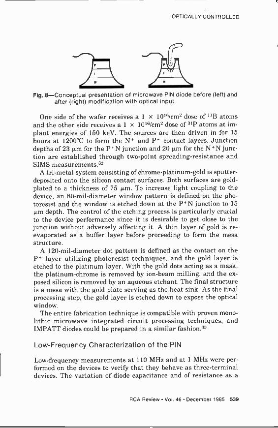
OPTICALLY CONTROLLED
Fig. 8-Conceptual presentation of microwave PIN diode before (left) and after (right) modification with optical input.
One side of the wafer receives a 1 x 10¹⁶/cm2 dose of "B atoms and the other side receives a 1 x 10¹⁶/cm2 dose of 3'P atoms at im- plant energies of 150 keV. The sources are then driven in for 15
hours at 1200°C to form the N+ and P+ contact layers. Junction depths of 23 p.m for the P N junction and 20 p.m for the N `N junc- tion are established through two -point spreading -resistance and SIMS measurements.32
A tri-metal system consisting of chrome -platinum -gold is sputter - deposited onto the silicon contact surfaces. Both surfaces are gold- plated to a thickness of 75 p.m. To increase light coupling to the device, an 80 -mil -diameter window pattern is defined on the pho- toresist and the window is etched down at the P N junction to 15
p.m depth. The control of the etching process is particularly crucial to the device performance since it is desirable to get close to the junction without adversely affecting it. A thin layer of gold is re - evaporated as a buffer layer before proceeding to form the mesa structure.
A 120 -mil -diameter dot pattern is defined as the contact on the P+ layer utilizing photoresist techniques, and the gold layer is etched to the platinum layer. With the gold dots acting as a mask, the platinum -chrome is removed by ion -beam milling, and the ex- posed silicon is removed by an aqueous etchant. The final structure is a mesa with the gold plate serving as the heat sink. As the final processing step, the gold layer is etched down to expose the optical window.
The entire fabrication technique is compatible with proven mono- lithic microwave integrated circuit processing techniques, and IMPATT diodes could be prepared in a similar fashion.33
Low -Frequency Characterization of the PIN
Low -frequency measurements at 110 MHz and at 1 MHz were per- formed on the devices to verify that they behave as three -terminal devices. The variation of diode capacitance and of resistance as a
RCA Review Vol. 46 December 1985 539
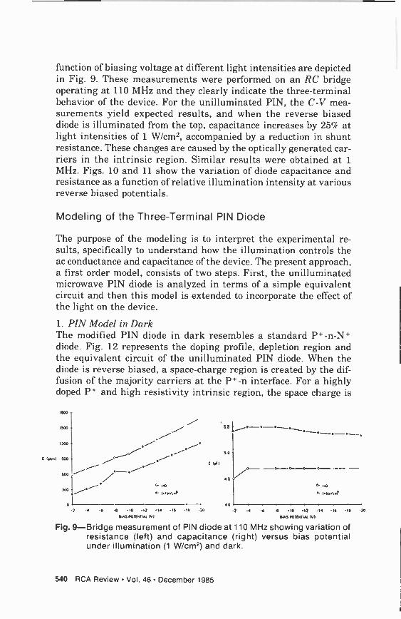
function of biasing voltage at different light intensities are depicted in Fig. 9. These measurements were performed on an RC bridge operating at 110 MHz and they clearly indicate the three -terminal behavior of the device. For the unilluminated PIN, the C -V mea- surements yield expected results, and when the reverse biased diode is illuminated from the top, capacitance increases by 25C% at light intensities of 1 W/cm2, accompanied by a reduction in shunt resistance. These changes are caused by the optically generated car- riers in the intrinsic region. Similar results were obtained at 1
MHz. Figs. 10 and 11 show the variation of diode capacitance and resistance as a function of relative illumination intensity at various reverse biased potentials.
Modeling of the Three -Terminal PIN Diode
The purpose of the modeling is to interpret the experimental re- sults, specifically to understand how the illumination controls the ac conductance and capacitance of the device. The present approach, a first order model, consists of two steps. First, the unilluminated microwave PIN diode is analyzed in terms of a simple equivalent circuit and then this model is extended to incorporate the effect of the light on the device.
1. PIN Model in Dark The modified PIN diode in dark resembles a standard P` -n -N - diode. Fig. 12 represents the doping profile, depletion region and the equivalent circuit of the unilluminated PIN diode. When the diode is reverse biased, a space -charge region is created by the dif- fusion of the majority carriers at the P' -n interface. For a highly doped P+ and high resistivity intrinsic region, the space charge is
/ / ' S3 .-.-.,,. /' ._.-.-_, 0 " / 50
C (0..,,9'30 ''''
C W) i -._.....-"'"' 0- ao0 .7 0-4 .../ 4 Pb
,00 . ,I5.,t.r i.wiam
-2 -. -6 -0 -10 -17 l. 10 -lb -20 40
1 -4 -0 -0 -10 -12 -I4 -16 -10 -10
Ou5P0tlelia lVI pu5P0IENN IV/
Fig. 9-Bridge measurement of PIN diode at 110 MHz showing variation of resistance (left) and capacitance (right) versus bias potential under illumination (1 W/cm2) and dark.
540 RCA Review Vol. 46 December 1985

OPTICALLY CONTROLLED
CI,(pI)
..lv
á .10
° .-70
o
o
o
Normalized light intensity 1/10 ; (10= 1 IV/cm')
Fig. 10-Bridge measurement of capacitance at 1 MHz.
O
mainly confined to the intrinsic region and is modulated by the re- verse bias potential (V). The equivalent circuit model of the PIN diode (Fig. 12, bottom) consists of ohmic contact resistance Re at the P+ and N 4- regions, space charge region's capacitance and resis- tance, C1 and R and capacitance and resistance of the unswept re- gions, C; and R. The parasitic inductances and fringing capaci- tances are not considered. These circuit elements can be written in terms of the device parameters:
C; = eA/(d - iv) R; = ((r;) -'(d - w)IA
C, = EA/to R = (air ' w/A
where
E = dielectric permittivity A = cross section of diode u' = depletion region width d = intrinsic region thickness
181
RCA Review Vol. 46 December 1985 541

.l .5 .4 .1 . .) .
* 5
Normalized light intensity 1/10 ; (Io= 1 11'/cm')
Fig. 11-Bridge measurement of conductance at 1 MHz.
(r1 = qµ,n = conductivity of the intrinsic region cry = qµ;p = conductivity of the depleted region n = N<< = the majority carrier density in the intrinsic region p = (ni)2/N<< = the minority carrier density in the depleted region
in thermal equilibrium.
Assuming uniform carrier distributions in the depleted and in- trinsic regions and an abrupt junction, the depletion width, w, can be expressed by the Schottky formula
w = I(2e1q)(V + (b)/1111/2 19]
where <b is the built-in junction potential and V is the reverse - biased voltage.
The impedance of the unilluminated (dark) diode is
RR(1 + jC,Ri) + R1(1 + "C;) Zd
1101 (1 + jwC,RR)(1 + jwC,R;)
542 RCA Review Vol. 46 December 1985

OPTICALLY CONTROLLED
NA
doping profile !
Nn
x
R F.,
F --Mey riM,-, R,
P+ o_,fv - __ivy - N.
!1 H c; c,
Fig. 12-Conceptual presentation of microwave PIN diode: (top) doping profile, (middle) Schottky depletion region, and (bottom) equiva- lent circuit model.
It is convenient to introduce normalized parameters:
t = cc/d, s = Ald, r = (r /(rJ, Go = (r1S,
Co = ES, T = Co/Go = e/ r;, z2 = (w T )2,
where t is normalized depletion width, s is a geometric factor (de- pending on design), Go is normalized conductance, Co is normalized capacitance, and T is the relaxation time. The conductance and susceptance can now be written
G G (1 - z2r)(1 - t + rt) + 227(1 + r)
X111 d= o (1 - t + rt)2 + (zr)2
(1 + r)(1 - t + rt) - r(1 - z2r) C,1 = Co
(1 - t + rt)2 (zr)2 1121
In practice, the carrier density in the depleted region is many orders of magnitude smaller than in the intrinsic region and there- fore the limiting case, r - x, prevails.
RCA Review Vol. 46 December 1985 543

2. PIN Diode Under Illumination When the PIN diode is illuminated (Fig. 13), electron -hole pairs are generated in the intrinsic and depleted regions and, assuming uni- form absorption, the carrier densities can now be written
nop = n + = n(1 + inln) = nS 1131
pop = p + ,p = p(1 + 4'p) = ph 114]
where Xn, _Sp are the optically generated excess electron and hole carrier densities which are related to the generation rates, g, and to the carrier lifetimes, (r) and (,,):
n = g (T) ,p = g (gip) (151
The optically generated carriers affect the device three ways. First of all, the conductivities of the intrinsic and depleted regions will be enhanced
(ai)op = 9µrnfi ((5)p = r11AtpK 1161
NA
doping profile
N
P'
J áN
((Np« eN)
w op d
ND
x
(C) )op (C, )op
Fig. 13-Conceptual presentation of microwave PIN diode under illumina- tion: (top) doping profile with the photo -generated carrier den- sity, (middle) Schottky depletion region shrinkage, and (bottom) equivalent circuit model.
544 RCA Review Vol. 46 December 1985

1.4
OPTICALLY CONTROLLED
3.2- VBIAs=-1DV o
3.0- VpT= -30V
2.8 1.3
2.6 o o
2.4- W u 1.2
2.2
2.0
-
- o -MEASURED 0- CALCULATED
u á
0
0 MEASURED
0- CALCULATED
1.8- o
< u 1.1
1.6
1.4 1A.
1.2
1.0
0.8 I 0.9 1 : 1 . 1 I
0 0.2 0.4 0.6 0.8 1.0 0 0.2 0.4 0.6 0.8 1.0
INTENSITY INTENSITY
Fig. 14-Relative variation of measured and calculated conductance (left) and capacitance (right) as a function of incident light intensity.
Secondly, the open circuit voltage will increase (induced photo - voltage), although this effect is small and may be neglected:
(d))op = d) - (kT/y) 1n(K) (1:,. 1171
Finally, the excess carrier density causes the space charge width, iv, to shrink,
u'op I(2E/q) (V + d)op)/(fr + á,1)11/2 w (8)- 1181
The equivalent circuit of the diode remains the same as for the un -
PIN diode
optical Input?
optical Input\
Coplanar MIC structure
Fig. 15-Conceptual presentation of optically controlled MIC phase shifter.
RCA Review Vol. 46 December 1985 545

o
PLANA/2.1 12:18pm OCT. 16 1984
/Phase: Light Off
hase: Light On Both
/Light On Both Diones "light Off
10.00 10.10 1.0.20 10.30 Frequency (GHz)
RP 1 - 0.000 cm RP 2 - 0.000 cm
Fig. 16-Network analyzer measurements of phase shifter (reverse biased at 20 V) in dark and under illumination (white light, 1 W/cm2).
illuminated PIN, but the circuit elements are now functions of the optical input.
¡ 4 1
1 - r - \ S - t ñ1 \ ñ1
+ r - I + rt -) + z2r --- 1 K/ K \ K1 K/
Go,, = Go 5311
(VZ - t 1191 rt -8)2 +Czr-2 K K
Co,, = Co VO
r1 z'1 + VT - t + rt-S - r-(1 - -)
(Vá
K K K SK
-t+rtsl2+l ( zr8l`1 2
1.201
where S and K are functions of the optical stimulation. The relative variation of the measured and calculated conduc-
tance and capacitance as a function of incident light intensity are shown in Fig. 14. These curves show a respectable agreement be- tween the measured and calculated variations.
546 RCA Review Vol. 46 Decembe 1985

OPTICALLY CONTROLLED
l T
(a) 0.291 pf
(b)
K= 150 ohm
0.35E p1
K'. 140 Ohm
Fig. 17-Predicted circuit parameters of the reverse -biased (-20 V) PIN diode model in the phase -shifter circuit configuration: (a) dark and (b) under white light illumination (1 W/cm2).
Microwave Measurements
The optically stimulated PIN diodes can function in microwave cir- cuits as phase -shifters, attenuators, limiters, modulators and switches. Two experiments were performed to assess the potential of the device for microwave applications. In the first experiment the diodes were incorporated into a coplanar MIC phase -shifter configu- ration, as shown in Fig. 15. The diodes were reverse biased at 20 V and illuminated by a white light source (1 W/cm2) which caused a phase -shift that was monitored on an error corrected network ana-
LED
Fig. 18-Conceptual presentation of Gunn oscillator circuit optically tuned by PIN switch.
RCA Review Vol. 46 December 1985 547

PIN ?Mr iWs 141129+Z J' iMZ 'ES
f.rb -~.m ,yrJl,
tr-m- a
raITE LI1E ̀ ; '1010/ . !1l Fig. 19-Shift in resonant frequency with white light. Left trace with no
illumination, right trace under white light illumination (1 W/cm2).
lyzer. A linear phase -shift of over 10° with a 15% bandwidth at 10 GHz was observed, as shown in Fig. 16. The phase -shift varied di- rectly with illumination. These results, which are considered pre- liminary since they were performed on the first set of specially pre- pared diodes, are encouraging since the light clearly controlled the phase shift of the microwave circuit. To enhance the phase shift as a
F n00 dam I T
v .' f/ V .0 ',Jl/v tr." 1! "V'+i l]` -'-'-
Fig. 20-Narrow band FM spectrum of Gunn oscillator (horizontal scale 100 MHz/div).
548 RCA Review Vol. 46 December 1985
OPTICALLY CONTROLLED
function of light intensity, the circuit was analyzed. Comparing the measured S -parameters and the equivalent circuit of Fig. 17, the high frequency R -C values of the PIN diode were obtained. Using these device parameters the phase shifter circuit was optimized using Super -Compact. The results of the optimization routine indi- cate that the limiting factor in the performance of the phase -shifter is the initial shunt capacitance of the diode prior to illumination, which is responsible for the high insertion loss. To improve the phase shifter performance, the size of the diode must be reduced.
In the second experiment the PIN diode was used as a "switch" in a MIC Gunn oscillator circuit, as shown in Fig. 18.27 When illumin- ated, the PIN bridges the gap between the resonator and the stub, thus changing the reactance of the circuit and hence its resonant frequency. Using this approach, the oscillator was tuned up to 60 MHz at 0.5 V biasing (Fig. 19), and frequency modulated at 300 MHz (Fig. 20).
Summary
This paper presents results of optically controlled microwave PIN diodes and DRO circuits. The device was fabricated from high -resis- tivity N -type Si and characterized at low frequencies (1, 110 MHz) and at X band. A simple preliminary model of the device, based on an equivalent circuit, was developed. The concept of using an opti- cally controlled microwave PIN diode as a phase shifter and a switch in microwave circuits was investigated.
In the case of the DRO, a thin photoconductive Si wafer was placed on top of a dielectric resonator disc in a dielectric resonator oscillator circuit illuminated by light. Optical tuning and FM mod- ulation of the DRO were demonstrated.
Acknowledgments
The authors wish to acknowledge the support of RCA (CIS Div.), the Naval Air Development Center, and the Commonwealth of Penn- sylvania's Ben Franklin Partnership grant.
References:
' J. R. Forrest and A. A. Salles, "Optics Control Microwaves," Microwave Systems News, June 1981, pp. 112-122. 2 Optical -Microwave Interaction Study," Report Prepared by Georgia Tech. for the Air Force, Report No. F33615-0-1709. 3 H. S. Sommers and F. K. Gateshell, Proc., IEEE, 54, p. 1553, 1966.
H. Jacobs et al., Proc., IEEE, 51, pp. 5-11, 1963.
RCA Review Vol. 46 December 1985 549

L. Hanlon and P. R. Herczfeld, "DC and Microwave Band Photoconductive Re- sponse in CdS Crystals," IEEE-MTT, 21, 1973. 6 A. M. Johnson and D. H. Auston, "Microwave Switching by Picosecond Photo- conductivity," IEEE J. Quantum Electronics, 11, pp. 283-287, 1975. 7 C. H. Lee, S. Mak, and A. P. DeFonzo, "Millimeter -Wave Switching by Optically Generated Plasma in Silicon," Electronics Letters, 14, pp. 733-734, 1978. 8 M. G. Li, W. L. Cao, V. K. Mathur, and C. H. Lee, "Wide Bandwidth, High Repeti- tion Rate Optoelectronic Modulation of Millimeter Waves in GaAs Waveguide," Electronics Letters, 18, pp. 454-456, 1982. 9 C. H. Lee, P. S. Mak and A. P. DeFonzo, "Optical Control of Millimeter Wave Prop- agation in Dielectric Waveguides," IEEE J. Quantum Electronics, 16, pp. 277-288, 1980. i0 P. R. Herczfeld, A. S. Daryoush. C. D'Ascenzo, A. Rosen, and M. Contarino, "Op- tically Tuned and FM Modulated Dielectric Resonator Oscillator," Proc., 14th Euro- pean Microwave Conf., Liege, Belgium, Sept. 1984, pp. 268-273. " H. W. A. Gerlach and R. Wellman, "The Behavior of a Pulsed Millimeter Wave (70 GHz) IMPATT Diode Oscillator During Laser Illumination," Proc. IEEE MTT-S Con- ference, pp. 70-72, 1980. 12 A. J. Seeds and J. R. Forrest, "Reduction of FM Noise in IMPATT Oscillators by Optical Illumination," Electronics Lett., 17, pp. 865-866, 1981. 13 H. P. Vyas, R. J. Gutman, and J. M. Borrego, "Leakage Current Enhancement in IMPATT Oscillators by Photoexcitation," Electronic Letters, 13, pp. 189-190, 1977. 14 H. P. Vyas, R. J. Gutman, and J. M. Borrego, "The Effect of Hole Versus Electron Photocurrent and Microwave -Optical Interactions in IMPATT Oscillators," IEEE Trans. Electron Devices, 26, pp. 232-234, 1979. '6 J. R. Forrest and A. J. Seeds, "Analysis of the Optically Controlled IMPATT (Opcad) Oscillator," Solid State and Electron Devices, 3, pp. 161-169, 1979. 16 H. Vyas, R. Gutman, and J. Borego, IEEE Trans. Electron Devices, ED -26, p. 232, 1979. 17 R. Kiehl, IEEE Trans. Microwave Theory Tech., MTT-28, p. 409, 1980. 18 H. W. Yen, M. K. Barnoski, R. G. Hunsperger, and R. T. Melville, Appl. Phys. Lett., 31, p. 120, 1977. 19 J. R. Forrest and A. J. Seeds, Electron. Lett., 14, p. 626, 1978. 20 A. J. Seeds and J. R. Forrest, "Initial Observations of Optical Injection Locking of an X -band IMPATT Oscillator," Electronics Lett., 14, pp. 829-830, 1978. 21J. R. Forrest and A. J. Seecs, "Optical Injection Locking of IMPATT Oscillators," Electronics Lett., 14, pp. 626-627, 1978. 22 W. Chen, N. E. Byer, M. Bendett, and R. Hunsperger, "Optical Control of IMPATT Diodes," SPIE, Vol. 477, Optical Technology for Microwave Applications, pp. 105-108, 1984. 23 A. A. Salles and J. R. Forrest, "Theory and Experiment for the GaAs MESFET Under Optical Illumination," Proc., 11th European Microwave Cont., Amsterdam, Netherlands. Sevenoaks, Kent, England, 904, 280-4.14. Microwave Exhibitions and Publishers, 1981. 24 F. J. Moncrief, Ed., "LEDs Replace Varactors for Tuning GaAs FETs," Micro- waves, 18, pp. 12-13, 1979. 25 A. A. Salles and J. R. Forrest, "Initial Observations of Optical Injection Locking of GaAs Metal Semiconductor Field Effect Transistor Oscillators," Applied Physics Lett., 398, pp. 392-394, 1981. 26 0. Ishihara, et al, "A Highly Stabilized GaAs FET Oscillator Using a Dielectric Resonator Feedback Circuit in 9-14 GHz," IEEE Trans. Microwave Theory and Tech., 28, pp. 817-824, Aug. 1980. 27 P. R. Herczfeld, A. Daryoush, and V. M. Contarino, "Optically tuned and Modu- lated Microwave Oscillator Circuits," SPIE, 517, Integrated Optical Circuit Eng. (1984). 28 J. D. Jackson, Classical Electrodynamics, 2nd Ed., John Wiley and Sons, Inc., New York, 1975. 29 Y. Shimoda, et al, "A Proposal of a New Dielectric Resonator Construction for MIC's," IEEE Trans. Microwave Theory and Tech., 31, pp. 527-532, July, 1983.
550 RCA Review Vol. 46 December 1985

OPTICALLY CONTROLLED
3° R. F. Harrington, Time -Harmonic Electromagnetic Fields, McGraw-Hill, Inc., New York, 1961. 3' R. H. Bube, Photoconductivity of Solids, John Wiley and Sons, Inc., New York, 1960. 32 A Rosen, R. U. Martinelli, A. Schwarzmann, G. J. Brucker, and G. A. Swartz, "High -Power Low -Loss PIN Diodes for Phase -Array Radar," RCA Review, 40, p. 22, March 1979. 33 A. Rosen, M. Caulton, P. Stabile, A. Gombar, W. Janton, C. P. Wu, J. Corboy, and C. Magee, "Silicon as a Millimeter -Wave Monolithically Integrated Substrate-A New Look," RCA Review, 42, p. 633, Dec. 1981.
RCA Review Vol. 46 December 1985 551

Patents Issued to RCA Inventors-Third Quarter 1985
July
R. C. Alig Cathode -Ray Tube Having Electron Gun With Three Focus Lenses (4,528,476) F. Aschwanden SECAM Modulator (4,528,527) P. C. Basile Switching Circuit Which is Self -Biased in One Mode of Operation (4,532,433) S. L. Bendell and C. A. Johnson Exposure Time Control for a Solid -State Color Camera (4,532,550) O. H. Bismarck Fast Switching Circuit (4,532,436) T. V. Bolger Television Receiver Having Picture Magnifying Apparatus (4,528,585) A. D. Cope Suppression of Edge Effects Arising in CCD Imager Field Registers (4,528,596) P. J. Coyle Apparatus and Method for Reducing Shock and Vibration Caused by Cartridge Loading (4,532,623) A. T. Crowley Fast Tuned Phase Locked Loop Frequency Control System (4,528,523) C. B. Dieterich Digital FM Ratio Detector With Gain -Controlled Filter (4,528,513) R. W. Fitts and E. M. Smith Electrostatic Shutter Tube Having Substantially Or- thogonal Pairs of Deflection Plates (4,528,447) R. T. Ford, J. M. Neilson, C. F. Wheatley, Jr., and N. W. Brackelmanns MOSFET With Perimeter Channel (4,532,534) R. A. Gange Cathode Structure for a Cathodoluminescent Display Devices (4,532,452) P. E. Haferl Television Receiver Standby Circuit (4,532,457) J. J. Hanak and G. E. Nostrand Series -Connected Photovoltaic Array and Method of Making Same (4,532,371) R. F. Haworth Repeater for Fiber Optic Bus Distribution System (4,527,286) L. L. Jastrzebski, A. C. Ipri, and A. G. Kokkas Method for Fabricating a Self -Aligned Vertical IGFET (4,530,149) J. Kane Method of Fabricating Lenticular Arrays (4,528,260) J. Kane Photodetector With Enharced Light Absorption (4,532,537) G. S. Kaplan and R. G. Setzer Apparatus and Method for Reducing Telephone Channel Power Loading (4,531,208) M. Kumar Frequency Multiplier Circuit for Producing Isolated Odd and Even Har- monics (4,531,105) M. E. Labib, C. C. Wang, and R. F. Poll Capacitance Electronic Disc Molding Com- position (4,532,074) H. G. Lewis, Jr. Apparatus for Demodulating Sampled Data Chroma Signals (4,527,188) H. G. Lewis, Jr. and A. L. Limberg Automatic Tint Correction With Reduced Color Saturation Error (4,528,586) H. G. Lewis, Jr. Digital Variable Group Delay Equalizer for a Digital Television Re- ceiver (4,531,149) V. Mangulis System and Method Employing Two Hop Spread Spectrum Signal Transmissions Between Small Earth Stations Via a Satellite and a Large Earth Sta- tion and Structure and Method for Synchronizing Such Transmissions (4,532,635) M. L. McNeely Method of Making a Video Disc from a Disc Preform (4,532,095) J. R. Nelson and B. F. Bogner EMI/RFI Shielding Composition (4,528,213) J. R. Nelson and R. A. Funari Impact Test Apparatus (4,531,401) P. C. Olsen Tuning Coil Structure (4,531,109) F. R. Ragland, Jr. Color Picture Tube Having Spring Supports for a Mask -Frame Assembly (4,528,475) R. J. Reilly and J. E. Gillberg Detection Circuitry With Multiple Overlapping Thresholds (4,529,892) G. Samuels Intaglio Printing Plate for Printing Serial Markings (4,530,286)
552 RCA Review Vol. 46 December 1985
J. R. Sandercock Technique for Verifying Genuineness of Authenticating Device (4,526,466) E. F. Steigmeier and H. Auderset Method for Determining the Phase of Phase Transformable Light Scattering Material (4,526,468) R. P. Stone Electron Gun Having Arc Suppression Means (4,531,075) L. K. White Multilayer Planarizing Structure for Lift -Off Technique (4,532,002) C. M. Wine Teletext Set -Top Converter With Transparent Mode (4,532,540) H. J. Wolkstein Optoelectronic Multiposition RF Signal Switch (4,530,573)
August
W. E. Babcock Multiple Scan Rate Deflection Circuit Incorporating Scan Compen- sation (4,536,684) T. V. Bolger Digital Signal Peaking Apparatus With Controllable Peaking Level (4,538,178) C. E. Deyer System for Inputting a Security Code to a Computer (4,538,027) R. A. Dischert and W. H. Meise Adaptive Digital Signal Coring Circuit (4,538,236) W. A. Dischert Method and Apparatus for Aligning a Chuck for Holding an Informa- tion Containing Disc Stylus (4,536,238) T. J. Faith, Jr. Method of Lowering Contact Resistance of Implanted Contact Re- gions (4,536,223) R. E. Fernsler and S. R. Vinekar Television Receiver Having Different Receiver Synchronizing Characteristics in Response to Television Signal (4,536,794) K. R. Frantz, R. A. Barnes, and B. G. Marks Resonant Degaussing Without Residual Magnetism (4,535,270) M. T. Gale and H. W. Lehmann Standardized Multi -Stack Dielectric -Layer Filter Blank and Method for Fabricating Color -Encoding Filter Therefrom (4,534,620) W. E. Harlan Non -Linear Dynamic Coring Circuit for Video Signals (4,536,796) G. E. Harris Apparatus for Thermoforming Dome -Shaped Actuating Elements for Membrane Switches (4,533,555) T. A. Hawkes Carrier Recovery Loop for Reception of Quadraphase Shift Keyed Signals (4,538,120) R. N. Hurst Color Modifier for Composite Video Signals (4,533,938) R. J. Maturo, D. Chin, and J. G. Henderson Television Receiver With Auxiliary On - Screen Display (4,536,797) M. M. Morrison Planar Microwave Circuit Component Mounting System (4,538,124) H. I. Moss Method for Lapping Diamond (4,532,737) W. W. Murphy, 3rd and S. V. Naimpally Demodulated Chrominance Signal Filter With Peaked Response (4,536,787) S. V. Naimpally Demodulated Chrominance Signal Filter Using Impedance Mis- matched Sections (4,536,788) R. P. Parker Additive Pulse Sampling Circuit (4,536,800) K. H. Powers System for Generating and Displaying a Compatible High Definition Television Signal by Progressive Scanning (4,533,951) J. J. Prusak Electroforming Apparatus (4,534,844) D. Raychaudhuri and L. N. Schiff Distortion Reducer for Companded Analog Systems (4,536,846) R. K. Reusch Method for Grounding a Pellet Support Pad in an Integrated Circuit Device (4,534,105) J. O. Sinniger and R. M. Peterson Multiplex Bus System for Controlling the Trans- mission of Data Between a Master Control Unit and a Plurality of Remotely Located Receiver -Transmitter Units (4,538,262) H. H. Westerman, Jr. Apparatus for Use in Trimming Molded Records (4,535,223) H. H. Westerman, Jr. Apparatus for Use in Trimming of Molded Records (4,535,224) D. H. Willis and D. W. Luz Switching Capacitor S -Correction Circuit (4,533,855)
September
A. Acampora Sampled Data Filter System as for a Digital TV (4,542,475) J. R. Ader Digital Color Filter Matrix for a Digital Television Receiver (4,542,402) T. V. Bolger Digital Signal Phase Measuring Apparatus as for a Phase -Locked Loop (4,543,600) J. A. Carvalho Multiple Input Voltage Power Controller (4,540,892) K. J. Chen Video Sync Validity Detector (4,543,614)
RCA Review Vol. 46 December 1985 553

H. N. Crooks and M. J. Kelly, Jr. Detection of Defects in a Circular or Spiral Diffrac- tion Grating (4,541,716) C. E. Deyer Switch Arrangement for Accessing a Computer (4,539,654) R. A. Duschl Charge Coupled Device Based System and Method for Inspecting and Modifying Images (4,542,404) H. Elabd CCD Imagers With Interleaved Image Resistors Using Opposed Directions of Charge Transfer (4,539,596) A. H. Firester and R. V. D'Aiello Method for Eliminating Defects in a Photodetector (4,543,171) M. A. Harger Tuning Control System for a Pair of Tuners Employing a Common Channel Skip Memory (4,539,711) F. Z. Hawrylo Flux -Free Photooetector Bonding (4,540,115) H. G. Lewis, Jr. Digital Deghosting System (4,542,408) N. O. Ny Mechanically -Actuated Touchbars and Touchplates Using Multiple -Clo- sure Switches (4,543,562) E. S. Poliniak High -Density Information Disc Lubricant (4,540,615) J. F. Schanne and L. D. Elliott Adaptive Analog -to -Digital Converter (4,540,974) S. Shwartzman Megasonic Cleaning Apparatus and Method (4,543,130) J. R. Tower Reducing Noise in Introducing Bias Charge Into Charge Transfer De- vices (4,541,068) D. H. Willis and R. T. Fling Analog -to -Digital Conversion Apparatus Including Double Dither Signal Sources (4,543,599) C. M. Wine Mechanically -Actuated Transparent Touchbars and Touchplates (4,543,563)
554 RCA Review Vol. 46 December 1985
AUTHORS
Joseph L. Abita received the BS and MS degrees from Fairleigh Dickinson University, and a PhD degree in Physics from Ohio University. He is currently a Re- search Scientist in the Microelectronics Division at COMSAT Laboratories, concentrating on monolithic microwave integrated -circuit development. Pre- viously, as Manager of the Microelectronic Fabrica- tion Technology Department, he directed personnel and operation integrating facilities, equipment, and processes. He has also designed and directed the in- stallation of several Inodern clean -room facilities. Prior positions, also in
the field of microelectronics, have been with General Electric, Eastman Kodak, and the Applied Physics Laboratory/Johns Hopkins University. He
is the author of a number of publications and holds several patents.
Erwin F. Belohoubek received a Diplom-lngenieur de- gree in 1953 and a PhD in Electrical Engineering in - 1955 from the Technical University in Vienna, Austria. From 1953 to 1955 he worked as a Research Assistant _ _ at the Institute for High -Frequency Techniques at the Technical University. r
In 1956 he joined the RCA Tube Division in Har- rison, NJ, as Research Engineer and, in 1957, trans- ferred to RCA Laboratories, Princeton, NJ, as a
Member of the Technical Staff. There he worked on the development of magnetrons, electrostatically and magnetically fo- cused traveling -wave tubes, and a crossed-fiela microwave delay tube.
In 1969 Dr. Belohoubek was placed in charge of a group working on
microwave hybrid integrated circuits. Currently, as Head, Microwave Cir- cuits Technology, at the Microwave Technology Center, he is responsible for the development of passive and active MIC circuits, including high - power transistor amplifiers, oscillators, phase shifters, linear bipolar and FET amplifiers, active microwave filters, various solid-state radars, and other microwave subsystems. He received an Outstanding Performance Award from the RCA Electronic Components Division in 1963, an RCA
Laboratories Outstanding Achievement Award in 1967, and the IEEE MTT
Microwave Applications Award in 1980. Dr. Belohoubek holds nine U.S. patents and has written more than 30
papers on microwave techniques, traveling -wave tubes, and microwave integrated circuits. He is a Fellow of the IEEE.
RCA Review Vol. 46 December 1985 555

John E. Bowers received the MS and PhD degrees in Applied Physics from Stanford University in 1978 and 1981, respectively. His dissertation involved the de- sign, fabrication, and demonstration of SAW signal-
-
processing devices. Since 1982, he has been working at Bell Laborato-
ries, Holmdel, NJ, investigating single -frequency high-speed detectors, lasers, and the microwave mod- ulationIlk of quaternary lasers. Previously, he was a re- search associate at Stanford University for one year, conducting research on single -mode fiber-optic devices, sensors, and signal processors. During one year at Honeywell, in 1979, he developed and studied an LPE system for the growth of HgCdTe.
Dr. Bowers is a member of Phi Beta Kappa, Tau Beta Pi, the Optical Society of America, and the American Physical Society, and is a Senior member of the IEEE. He is a recipient of Sigma Xi's Thomas F. Andrews prize for undergraduate research.
Charles A. Burrus, Jr., received the BS degree. cum laude, from Davidson College in 1950. the MS degree from Emory University in 1951, and the PhD degree from Duke University in 1955, all in Physics. At Duke he studied under Texas Company and Shell Company Fellowships, and was empJoyed as a Research Asso- ciate in 1954-55.
In 1955 he joined the Technical Staff of AT&T Bell Laboratories, Holmdel, NJ, where his work initially was concerned with the millimeter- and submilli- meter -wave region of the spectrum (microwave spectroscopy and various types of semiconductor diodes for millimeter -wave use) and later with sources and detectors for lightwave communication (fiber -compatible LEDs, lasers, and PIN phctodiodes). Currently he is working on high- speed semiconductor devices for lightwave communications in the 1- to 1.6-µm wavelength region, and on the effects of deuterium and hydrogen in optical fibers.
Dr. Burrus is a member of Phi Beta Kappa, Sigma Pi Sigma, and Sigma Xi. He is a Fellow of the American Association for the Advancement of Science, the American Physical Society, the Institute of Electrical and Electronics Engineers, and the Optical Society of America. He is the recip- ient of the 1982 David Richardson Medal in applied optics from the Op- tical Society of America and the Distinguished Technical Staff Award (1982) from AT&T Bell Laboratories.
Alejandro Chu received the BSc degree in 1970, and the MSc and EE degrees in 1972, all in Electrical Engi- neering, from the Massachusetts Institute of Tech- nology. He received the PhD degree from Stanford University in 1977. His dissertation was in the field of ion implantation.
From 1972 to 1978, he worked at Hewlett-Packard Company onthe development of wideband 1 -to 18f GHz sweeper and microfrequency multipliers, and of wideband amplifiers. In 1975, at the Hewlett-Packard Technology Center, he was responsible for the characterization of GaAs FETs and, later, the fabrication of GaAs integrated circuits. From 1978 to 1984 he was a member of the technical staff at the MIT Lincoln Labora- tory, where he was responsible for developing GaAs devices and mono- lithic circuits for a millimeter -wave transceiver. He has recently joined the Corporate Technology Center of M/A-COM Inc.
556 RCA Review Vol. 46 December 1985

Brian J. Clifton received the BSc degree with honors in Electrical Engineering and the PhD degree from the University College of North Wales, Bangor, in 1961 and 1964 respectively.
From 1964 to 1966 he was a Visiting Assistant Pro- fessor in the Department of Electrical Engineering, MIT, Cambridge. In 1966 he joined the MIT Lincoln Laboratory, Space Communications Division, to en- gage in research into the microwave behavior of semi- conductor devices and circuits and the development of low -noise GaAs Schottky -barrier diodes for the LES -8/9 millimeter - wave communications systems. He also worked on low -noise parametric amplifiers and mixers for use at millimeter -wave frequencies.
In 1976 Dr. Clifton joined the Solid State Division for the specific pur- pose of developing Schottky -barrier diodes for submillimeter applica- tions. His current work continues in this area with the development of quasi -optical receiver systems and monolithic integrated circuits for the millimeter and submillimeter regions.
William E. Courtney received the BSc degree with honors in Physics, and the PhD degree in Electrical Engineering from the Queens' University of Belfast, N. Ireland, in 1959 and 1963, respectively.
From 1963 to 1966, he was a department of Scien- tific and Industrial Research and Ministry of Aviation Post -Doctoral Research Fellow in the Department of Electrical Engineering, University of Leeds, England. From 1966 to 1968, he was a Post -Doctoral Fellow in the Centre for Materials Science and Engineering, Massachusetts Institute of Technology; currently he is a member of the Experimental Systems Group of the MIT Lincoln Laboratory, Lexing- ton, MA.
Afshin S. Daryoush received the BS degree from Case Western Reserve University and the MS degree from Drexel University, both in Electrical Engineering. He is currently working toward the PhD degree at the De- partment of Electrical Engineering, Drexel University, and is expected to graduate in June 1986.
His interests lie in the field of optical control of mi- crowave devices and subsystems, with emphasis on optically controlled phased -array antennas for air- 3j'`' borne applications. Mr. Daryoush has authored or coauthored more than 20 conference and journal publications on the subject of short -haul fiberoptic communication, high-speed laser diodes and detectors, and the optical control of passive and active microwave circuits and devices.
.-k 4 r
Ede P. Enobakhare received the BS and MS degrees in Electrical Engineering from the University of Mis- sissippi in 1979 and 1980, respectively. In 1980, he joined COMSAT Laboratories to engage in the design and development of MIC and MMIC LNAs. Since March 1985, he has been with Amplica, COMSAT Technology Products Division, where he is involved in developing low -noise amplifier products.
RCA Review Vol. 46 December 1985 557

Morris Ettenberg received a BA degree in Mathe- matics in 1935 and an MS degree in Mathematics in Education in 1936, both from City College of the City University of New York. He earned a PhD in Physics from New York University in 1950.
From 1942 to 1945 he worked as a radar engineer at the U.S. Navy Yard in Brooklyn. He then joined Sperry Gyroscope as an engineer and, from 1955 to 1958, headed Sperry's Department of Power TWT Develop- ment. During 1958-63 Dr. Ettenberg served as a re- search professor at the Polytechnic Institute of New York. He then joined the faculty of City College and, from 1968 to 1973, served as Chairman of the Electrical Engineering Department.
In addition to being a faculty member at City College, Dr. Ettenberg has been a consultant for RCA Laboratories since 1980. His research and publications are in the field of microwave tubes and semiconductor de- vices. He is a Life Senior member of the IEEE.
Masumi Fukuta, Manager, Microwave and High Speed Semiconductor Device Development Department, Fu- jitsu, Ltd., Japan, received a BS degree from the Na- goya Institute of Technology in 1963, and the PhD de- gree from Nagoya University in 1977, both in Elec- trical Engineering. He joined Kobe Industries Company in 1963 and Fujitsu, Ltd., in 1968, when Fu- jitsu merged with Kobe Industries. He was engaged in *¡ developing Si rf power transistors, ICs, and MOS ` FETs. In 1967 he invented the Mesh Emitter Transistor (MET) and developed it to the industrial stage. Now, METs are widely ap- plied in the high -power stage of transmitters operated in the UHF range.
Since 1972, Dr. Fukuta has worked on the development of low -noise and power GaAs FETs and GaAs ICs. In 1975 he received a prize from the Science and Technology Minister of Japan for his work on power GaAs FETs. This prize has been established by the government for scientists and engineers who perform outstanding research.
Peter R. Herczfeld received a BS degree in Physics from Colorado State University in 1961 and, from the University of Minnesota, an MS in Physics in 1963 and i a PhD in Electrical Engineering in 1967. Since 1967 he i^ has been on the faculty of Drexel University, where he is a Professor of Electrical and Computer Engi- neering. He has taught 20 different courses at the graduate and undergraduate levels and has lectured extensively in this country and in 10 foreign countries. He coordinates the microwave and electrooptics pro- J / gram at Drexel.
Dr. Herczfeld served as project director and principal investigator for 21 projects sponsored by DOD, NSF, NASA, DOE, and private industry. He has published more that 70 papers in solid-state electronics, microwaves, solar energy, and biomedical engineering. He is a member of the APS, IEEE, SPIE, and the International Solar Society.
558 RCA Review Vol. 46 December 1985

Yasutake Hirachi received the BS and MS degrees in Electrical Engineering from Tokyo University of Agri- culture and Technology, Tokyo, Japan, in 1968 and 1970, respectively. In 1979 he received the PhD de- gree from the Tokyo Institute of Technology, Tokyo, .
Japan. From 1970 to 1971 he was a Research Associate at
the Tokyo Institute of Technology, where he worked on machine control by means of laser diodes. In 1971
fly
he joined Fujitsu Laboratories, Ltd., Kawasaki, Japan. There he worked, until 1978, on the research and development of both Si and GaAs IMPATT diodes. He then joined the development group of power GaAs FETs, where he was responsible for the design, fabrication, and characterization of these devices. In 1980 Dr. Hirachi moved from Fujitsu Laboratories to Fujitsu Ltd.. Microwave Semicon- ductor Devices Division, where he was engaged in the development of high -frequency, high -power GaAs FETs. In 1983 he was transferred to Fu- jitsu Laboratories, Compound Semiconductor Laboratory, where he worked on the research and development of the High -Electron :Mobility Transistor (HEMT). He is currently a supervisor in the HEMT Section.
Dr. Hirachi received the 1978 Watanabe Award for outstanding contri- butions in the field of semiconductor research and development from HANDOTAI SHINKOKAI. He is a member of the Institute of Electronics and Communication Engineers of Japan, and the Electron Devices Group of the IEEE.
Ho -Chung Huang received a BS degree from National Taiwan University in 1959, and a PhD degree from Cornell University in 1967. As Executive Director of the Microelectronics Division at COMSAT Laborato- ries, he is responsible for developments in microwave semiconductor materials, discrete devices, and mon- olithic integrated circuits for satellite and terrestrial applications. From 1969 to 1983 he was Head of Mi- crowave Processing Technology at RCA Laboratories.
11' Dr. Huang is a Senior Member of the IEEE. He has published and presented numerous technical papers, and has been granted several U.S. patents. He was a recipient of the 1980 RCA Labora- tories Outstanding Achievement Award for development of space -quali- fied, solid-state GaAs FET power amplifiers for use ín RCA SATCOM satel- lites. He was also granted the 1983 David Sarnoff Award for Outstanding Technical Achievement, RCA's highest technical honor, for a team effort leading to the first commercial solid-state microwave power amplifier in
space.
Hing-Loi A. Hung received the SB degree in Electrical Engineering from the Massachusetts Institute of Technology in 1968, and the MS and PhD degrees from Cornell University in 1970 and 1974, respectively. As Manager of the Monolithic Microwave Techniques Department of the Microelectronics Division at COMSAT Laboratories, he is involved in the research and development of satellite and earth station com- munications technologies. His recent studies have in- cluded GaAs ICs (analog and digital), thermoelectric- ally coiled LNAs, nonlinearities and low -frequency noise in MESFETs, and
RCA Review Vol. 46 December 1985 559

broadband design techniques. He participated in satellite transponder de- sign reviews for the INTELSAT V, VI, and STC programs, and worked on the COMSTAR 20/30-GHz beacon project. Previously, he worked on mi- crowave components at Bunker -Ramo Corporation, the MIT Research Laboratory of Electronics, and Chu Associates. Dr. Hung is a Senior Member of the IEEE and a member of Sigma Xi. He was Vice -Chairman and Chairman of the Washington IEEE Electron Devices Society from 1980 to 1982.
Christoph E. Mahle received the Dipl. Ing. in Electrical Engineering and the Dr. Sc. Techn. from the Swiss Federal Institute of Technology (ETH) in 1961 and 1966, respectively. Currently, as Executive Director of the Microwave Technology Division at COMSAT Labo- ratories, he directs research and development in mi- croWave systems and circuits for satellites and earth stations, monolithic microwave integrated circuits, analysis and verification of satellite transponder per- formance,
, 'a;, satellite and earth station antennas, optical ;
communications and wave propagation. Earlier, Dr. Mahle served as Acting Director of the newly formed Microelectronics Division. which was set up to combine COMSAT's efforts in analog and digital GaAs integrated circuits. He directed several projects and studies such as development of the first contiguous -band satellite multiplexer, of the first 14-GHz, 120- Mbit/s direct demodulating DQPSK receiver, and of systems for in -orbit testing and monitoring of communications satellites. He designed and evaluated communications transponders for the INTELSAT IV, IV-A,V, and COMSTAR programs, and was responsible for the design, development, and testing of the transponder orbited on ATS-6 as part of the COMSAT Propagation Experiment. In addition, he has been a major contributor to the state of the art of automated satellite in -orbit measurements.
Prior to joining COMSAT in 1968, Dr. Mahle was engaged in research and teaching at the Microwave Laboratory of the Swiss Federal Institute of Technology, Zurich, Switzerland. He is a member of the IEEE, has pub- lished several papers, and has been awarded a number of U.S. patents.
Leonard J. Mahoney graduated from Wentworth Insti- tute, Boston, MA, in 1964. He received the AA and BA degrees (with honors) in mechanical engineering from Northeastern University, Boston. in 1973 and 1975, respectively.
In 1972 Mr. Mahoney joined the Lincoln Laboratory, Massachusetts Institute of Technology, Lexington, MA, where he has worked on the fabrication of a number of microwave devices including GaAs IM- PATT diodes, surface -oriented mixer diodes, and \ \ FETs. He is currently an Assistant Staff Member in the Microelectronics group, working on process development and the fabrication of GaAs ICs for millimeter -wave applications.
Philip J. McNally received a BS degree in Physics from St. Francis College in 1959, and pursued grad- uate studies at Pennsylvania State University and Northeastern University. He joined COMSAT Labora- tories in 1974 and is currently a Research Scientist in the Microelectronics Division, where he has been in- volved in research on IMPATT diodes, ion -implanted GaAs FETs, and Schottky barriers. At present he is re-
560 RCA Review Vol. 46 December 1985

sponsible for the development of ion -implantation technology for GaAs integrated circuits.
Prior to joining COMSAT, at Ion Physics Corporation and at Honeywell, Inc., Mr. McNally was an early contributor in the field of ion implantation and its application to semiconductor device technology. These activities included both silicon and compound semiconductor devices, the latter emphasizing photodetector development. He is a member of the IEEE, Sigma Pi Sigma, and Delta Epsilon Sigma.
Markus Nowogrodzki was graduated with the degrees of Bachelor of Electrical Engineering, cum laude, in 1948, and Master of Electrical Engineering, in 1951, P N
both from the Polytechnic Institute of New York. From 1948 until 1951, he was a Microwaves Engi-
neer at Hazeltine Corp., working on microwave cavi- ties and test procedures for IFF systems. From 1951 until 1955, he was with Amperex Electronic Corp., - where he helped establish the magnetron develop- ment department and rose to the position of Super- vising Engineer, Magnetron Development. In 1955, he joined RCA Elec- tronic Components, engaged in the development and manufacturing of magnetrons, microwave triodes, traveling -wave tubes, and solid-state subsystems. As Manager, Traveling -Wave Tube Operations, he supervised a department comprising design, manufacturing, applications, and pro- gram -control activities.
During 1967-73, Mr. Nowogrodzki worked in microwave tube and product management at North American Philips and Polyflon Corpora- tion. In 1973, he rejoined RCA as Manager, Division Liaison, at the Micro- wave Technology Center, RCA Laboratories, Princeton, NJ. He is now Head, Subsystems and Special Projects, Microwave Technology Center.
Mr. Nowogrodzki has written more than 20 papers on various aspects of microwave component design and applications. He holds seven U.S. pa- tents. He is a member of the New York Academy of Sciences, Eta Kappa Nu, and Tau Beta Pi, and a Senior member of the IEEE.
Arye Rosen received the BSEE degree cum laude from Howard University in 1963 and the MScE degree from Johns Hopkins University (which he attended on a Gillman Fellowship) in 1965. He was an instructor at Johns Hopkins during 1963-64.
From 1964 to 1967, Mr. Rosen was concerned with systems design at General Telephone and Electronics International, Inc., and American Electronics Labora- tories, Inc.
In 1967, he joined RCA Laboratories, Princeton, NJ, as a Member of the Technical Staff in the Microwave Technology group. Mr. Rosen is responsible for the research and development of millimeter - wave devices and circuits, as well as rf silicon devices, such as PIN and varactor, and was extensively involved in the thermal studies of those de- vices. His work on integrated diode arrays paved the way for power com- bining in microwave and millimeter waves. He received a 1972 RCA Labo- ratories Outstanding Achievement Award for a team effort in the develop- ment of S -band TRAPATT amplifiers and, in 1982, an individual RCA Laboratories Outstanding Achievement Award for developing high-perfor- mance silicon PIN diodes for application to communication systems.
From 1970 to 1971, on leave of absence from RCA, Mr. Rosen was en- gaged in research in the Division of Cardiology (on a departmental Fel- lowship) at Jefferson Medical College ir. Philadelphia. There he received
r++-. ,.
RCA Review Vol. 46 December 1985 561

the degree of MSc in Physiology and later was appointed an Associate in Medicine. He now holds an appointment of Adjunct Professor at Drexel University, in the Department of Electrical and Computer Engineering.
Mr. Rosen is the author or coauthor of more than 60 technical papers and presentations and holds 21 U.S. patents in the microwave field.
He is a member of Tau Beta Pi, Sigma Xi, and the Association of Profes- sional Engineers of British Columbia (Canada), as well as a Senior member of the IEEE. He has been included in Who's Who in Technology Today.
Paul J. Stabile received the BEEE degree summa cum laude from Manhattan College in 1979 and the MSEE degree from Rutgers University in 1982. In 1979 he joined the RCA Engineering Rotation program. His assignments included microwave amplifier design, digital circuit development, and computer -aided de- sign techniques for VLSI circuitry. Later that year, he joined the Microwave Technology Center at RCA Lab- oratories, Princeton, NJ.
Mr. Stabile, as a Member of the Technical Staff, has been engaged in the research and development of microwave and milli- meter -wave devices and circuits, including millimeter -wave IMPATT diodes, oscillators and amplifiers, high -power PIN diodes, frequency mul- tipliers, phase shifters, silicon millimeter -wave integrated circuits, and op- tically controlled microwave devices.
He has authored or coauthored more than 20 technical papers and has one U.S. patent pending. Mr. Stabile is a member of Etta Kappa Nu, Tau Beta Pi, and the IEEE.
Herbert J. Wolkstein joined RCA Microwave Opera- tions in 1955 after seven years as Project Engineer in the Research Laboratories of National Union Electric Corporation, where he worked on the design of spe- cial-purpose beam -deflection and high-speed com- puter -switching tubes. In 1961, he became Manager, TWT Design and Development. In 1964, as Manager of Microwave Advanced Product Development, Mr. Wolkstein directed a group in advanced development and applications work on TWTs and solid-state de- vices. Since that time he has held various management positions in RCA until 1975; then he became a Member, Technical Staff, at the Microwave Technology Center, RCA Laboratories, Princeton. NJ.
In his present position of Head, Space and Countermeasure Programs. Mr. Wolkstein is engaged in the development and applications of solid- state microwave devices and subsystems. For his contributions to a team effort leading to the first commercial solid-state microwave power ampli- fiers in space he shared an RCA Laboratories Outstanding Achievement Award in 1982 and a David Sarnoff Award for Outstanding Technical Achievement, RCA's highest honor, in 1983. He has been awarded 15 U.S. patents in the electron -tube and solid-state fields.
Mr. Wolkstein is a Senior member of the IEEE's Professional groups on Electron Devices and Microwave Theory and Techniques.
40,
562 RCA Review Vol. 46 December 1985

Index, Volume 46, 1985
March
3 Elastic Light Scattering Techniques for Semiconductor Technology E. F. Steigmeier and H. Auderset
19 Characterization of Heteroepitaxial Silicon on Sapphire by UV Reflectometry M. T. Duffy, G. W. Cullen, R. A. Soltis, G. Harbeke, and J. R. Sandercock
34 Optical Profilometer for Measuring Surface Contours of 1 to 150 Microns Depth H. P. Kleinknecht and H. Meier
56 Rapid Evaluation of Submicron Laser Spots M. T. Gale and H. Meier
70 A Dynamic Antivibration Support J. R. Sandercock, M. Tgetgel, and E. Meier
81 Megasonic Particle Removal from Solid -State Wafers S. Shwartzman, A. Mayer, and W. Kern
106 Patents.
109 Authors
June
117 Optimized Chemical Vapor Deposition of Borophosphosilicate Glass Films Werner Kern, W. A. Kurylo, and C. J. Tino
153 The Limitation of Short -Channel -Length N+-Polysilicon-Gate CM3S ICs Sheng Teng Hsu
163 Barrier -Height Measurements of Tantalum Silicide on Silicon Sheng Teng Hsu and Jer-Shen Maa
170 Preparing Master Grooves for Lapping Discs Used in Micromachining of VideoDisc Styli W. R. Roach and I. Gorog
200 Measurement of the Thermal Resistance of Packaged Laser Diodes J. J. Hughes, D. B. Gilbert, and F. Z. Hawrylo
214 A Comparison of the Flux -Corrected Transport Method With Other Low - Dispersive Schemes for the Two -Dimensional Linear Advection Equation Harvey P. Miller
240 Optoelectronic Performance Issues in Fiber -Optic Communications D. J. Channin
270 Patents
273 Authors
September
281 An Introduction to Modeling and Simulation Robert Amantea
RCA Review Vol. 46 December 1985 563

289 Integrated Simulation of CMOS Transistors Robert Amantea and Beatrice Hwong
308 A SPICE II Subcircuit Representation for Power MOSFETs Using Empirical Methods Gary M. Dolny, Harold P. Ronan, Jr. and C. Frank Wheatley, Jr.
321 N-FET, A New Software Tool for Large -Signal GaAs FET Circuit Design Walter R. Curtice and Morris Ettenberg
341 New Algorithms for the Automated Microwave -Tuner Test System Stewart M. Perlow
356 Simulation of Microlithographic Resist Processing Using the SAMPLE Program Dietrich Meyerhofer
376 Active -Array Antenna Beam Shaping for Direct Broadcast Satellites and Other Applications Samuel H. Colodny and Roger L. Crane
393 A Program to Test Satellite Transponders for Spurious Signals Benjamin R. Epstein
407 Patents
411 Authors
December
419 Microwave Technology-A Brief Overview Markus Nowogrodzki
421 Millimeter -Wave Monolithic Circuits for Receiver and Transmitter Applications A. Chu, W. E. Courtney, L. J. Mahoney, and B. J. Clifton
431 GaAs FET MMIC Low -Noise Amplifiers for Satellite Communications H. -L. Hung, E. Enobakhare, J. Abita, P. McNally, C. Mahle, and H. Huang
441 Recent Developments in Microwave GaAs FETs in Japan Masumi Fukuta and Yasutake Hirachi
464 Miniature Microwave Hybrid Circuits Erwin F. Belohoubek
484 Advanced Traveling -Wave Tubes for Satellite Applications Herbert J. Wolkstein
496 Optoelectronic Components arid Systems with Bandwidths in Excess of 26 GHz John E. Bowers and Charles A. Burrus
510 Microwave Hyperthermia and Radiometry: One -Dimensional Computer Models Morris Ettenberg
528 Optically Controlled Microwave Devices and Circuits P. R. Herczfeld, A. S. Daryoush, A. Rosen, P. Stabile, and V. M. Contarino
552 Patents
555 Authors
563 Index, Volume 46, 1985
564 RCA Review Vol. 46 December 1985

Index to Authors, Volume 46, 1985
J. Abita GaAs FET MMIC Low -Noise Amplifiers for Satellite Communications, December. p. 431
R. Amanfea An Introduction to Modeling and Simulation. September, p. 281
-Integrated Simulation of CMOS Transistors, September, p. 289 A. Auderset Elastic Light Scattering Techniques for Semiconductor Technology, March, p. 3
E. F. Belohoubek Miniature Microwave Hybrid Circuits, December, p. 464
J. E. Bowers Optoelectronic Components and Systems with Bandwidths in Excess of 26 GHz,
December. p. 496 C. A. Burrus Optoelectronic Components and Systems with Bandwidths in Excess of 26 GHz,
December. p. 496 D. J. Channin Optoelectronic Performance Issues in Fiber -Optic Communications, June, p. 240
A. Chu Millimeter -Wave Monolithic Circuits for Receiver and Transmitter Applications, De-
cember, p. 421 B. J. Clifton Millimeter -Wave Monolithic Circuits for Receiver and Transmitter Applications, December, p. 421
S. H. Colodny Active -Array Antenna Beam Shaping for Direct Broadcast Satellites and Other Applications, September, p. 376 V. M. Contarino Optically Controlled Microwave Devices and Circuits, December, p. 528 W. E. Courtney Millimeter -Wave Monolithic Circuits for Receiver and Transmitter Applications, December. p. 421
R. L. Crane Active -Array Antenna Beam Shaping for Direct Broadcast Satellites andOther Ap-
plications, September, p. 376 G. W. Cullen Characterization of Heteroepitaxial Silicon on Sapphire by UV Reflectometry, March, p. 19 W. R. Curtice N-FET, A New Software Tool for Large -Signal GaAs FET Circuit Design, Sep- tember, p. 321 A. S. Daryoush Optically Controlled Microwave Devices and Circuits, December, p. 528 G. M. Dolny A SPICE II Subcircuit Representation for Power MOSFETs Using Empirical Methods, September, p. 308 M. T. Duffy Characterization of Heteroepitaxial Silicon on Sapphire by UV Reflectometry, March, p. 19 E. Enobakhare GaAs FET MMIC Low -Noise Amplifiers for Satellite Communications, De-
cember, p. 431 B. R. Epstein A Program to Test Satellite Transponders for Spurious Signals, September, p. 393 M. Ettenberg N-FET, A New Software Tool for Large -Signal GaAs FET Circuit Design, Sep- tember, p. 321 -Microwave Hyperthermia and Radiometry: One -Dimensional Computer Models, December, p. 510 M. Fukuta Recent Developments in Microwave GaAs FETs in Japan, December, p. 441
M. T. Gale Rapid Evaluation of Submicron Laser Spots. March, p. 56 D. B. Gilbert Measurement of the Thermal Resistance of Packaged Laser Diodes, June, p. 200
I. Gorog Preparing Master Grooves for Lapping Discs Used in Micromachining of VideoDisc Styli, June, p. 170 G. Harbeke Characterization of Heteroepitaxial Silicon on Sapphire by UV Reflectometry, March, p. 19 F. Z. Hawrylo Measurement of the Thermal Resistance of Packaged Laser Diodes, June. p. 200 P. R. Herczfeld Optically Controlled Microwave Devices and Circuits. December, p. 528 Y. Hirachi Recent Developments in Microwave GaAs FETs in Japan, December, p.441 S. T. Hsu The Limitation of Short -Channel -Length N+-Polysilicon-Gate CMOS ICs, June, p. 153
-Barrier -Height Measurements of Tantalum Silicide on Silicon. June, p. 163
H. Huang GaAs FET MMIC Low -Noise Amplifiers for Satellite Communications, December, p.
431 J. J. Hughes Measurement of the Thermal Resistance of Packaged Laser Diodes, June, p. 200 H. -L. Hung GaAs FET MMIC Low -Noise Amplifiers for Satellite Communications, December, p. 431 B. Hwong Integrated Simulation of CMOS Transistors, September, p. 289 W. Kern Megasonic Particle Removal from Solid -State Wafers, March, p. 81
-Optimized Chemical Vapor Deposition of Borophosphosilicate Glass Films, June, p. 117
H. P. Kleinknecht Optical Profilometer for Measuring Surface Contours of 1 to 150 Microns Depth, March, p. 34 W. A. Kurylo Optimized Chemical Vapor Deposition of Borophosphosilicate Glass Films, June, p. 117
RCA Review Vol. 46 December 1985 565

J. -S. Maa Barrier -Height Measurements of Tantalum Silicide on Silicon, June, p. 163 C. Mahle GaAs FET MMIC Low -Noise Amplifiers for Satellite Communications, December, p. 431 L. J. Mahoney Millimeter -Wave Monolithic Circuits for Receiver and Transmitter Applications, December, p. 421 A. Mayer Megasonic Particle Removal from Solid -State Wafers, March, p. 81 P. McNally GaAs FET MMIC Low -Noise Amplifiers for Satellite Communications, December, p. 431
E. Meier A Dynamic Antivibration Support, March, p. 70 H. Meier Optical Profilometer for Measuring Surface Contours of 1 to 150 Microns Depth, March, p. 34 -Rapid Evaluation of Submicron Laser Spots, March, p. 56 D. Meyerhofer Simulation of Microlithographic Resist Processing Using the SAMPLE Pro- gram, September, p. 356 H. P. Miller A Comparison of the Flux -Corrected Transport Method With Other Low -Dispersive Schemes for the Two -Dimensional Linear Advection Equation, June, p. 214 M. Nowogrodzki Microwave Technology-A Brief Overview, December, p. 419 S. M. Perlow New Algorithms for the Automated Microwave -Tuner Test System, September. p. 341 W. R. Roach Preparing Master Grooves for Lapping Discs Used in Micromachining of Video -
Disc Styli, June, p. 170 H. R. Ronan, Jr. A SPICE II Subcircuit Representation for Power MOSFETs Using Empirical Methods, September, p. 308 A. Rosen Optically Controlled Microwave Devices and Circuits, December. p. 528 J. R. Sandercock Characterization of Heteroepitaxial Silicon on Sapphire by UV Reflecto- metry, March, p. 19 -A Dynamic Antivibration Support. March, p. 70 S. Shwartzman Megasonic Particle Removal from Solid -State Wafers, March. p. 81 R. A. Soltis Characterization of Heteroepitaxial Silicon on Sapphire by UV Reflectometry, March, p. 19 P. Stabile Optically Controlled Microwave Devices and Circuits, December, p. 528 E. F. Steigmeier Elastic Light Scattering Techniques for Semiconductor Technology, March, p. 3 M. Tgetgel A Dynamic Antivibration Support, March. p. 70 C. J. Tino Optimized Chemical Vapor Deposition of Borophosphosilicate Glass Films, June. p. 117 C. F. Wheatley, Jr. A SPICE II Subcircuit Representation for Power MOSFETs Using Empirical Methods, September, p. 308 H. J. Wolkstein Advanced Traveling -Wave Tubes for Satellite Applications, December, p. 484
566 RCA Review Vol. 46 December 1985

-

-

STATEMENT OF OWNERSHIP Statement of Ownership, Management and Circulation (Act of August 12, 1970, Section 3685, Title 39, United States Code).
1. Title of Publication: RCA REVIEW, Publication No. 00336831.2. Date of Filing. October 9, 1985. 3. Frequency of Issue: Quarterly. No. of Issues Published Annually: Four (4). Annual Subscription Price: $12.00. 4. Complete Mailing Address of Known Office of Publication: RCA-David Sarnoff Research Center, Princeton, Mercer County, New Jersey 08540. 5. Complete Mailing Address of the Headquarters of General Business Offices of the Publisher: RCA-David Sarnoff Research Center, Princeton. Mercer County, New Jersey 08540. 6. Full Names and Complete Mailing Address of Publisher. Editor, and Managing Editor: Publisher-RCA Corporation, RCA Laboratories, Princeton. New Jersey 08540. Editor/Managing Editor-Ralph F. Ciafone. RCA, David Sarnoff Research Center, Princeton, New Jersey 08540. 7. Owner: The Chase Manhattan Bank, N.A., One Chase Man- hattan Plaza, New York, NY 10005: Bankers Trust Company, P.O. Box 704. Church Street Station, New York, NY 10015: State Street Bank and Trust Co.. P.O. Box 1713. Boston, MA 02105; Merrill. Lynch. Pierce. Fenner and Smith. Inc., 70 Pine Street, New York, NY 10005: Manufacturers Trust Company. 600 Fifth Avenue, New York. NY 10020; Morgan Guaranty Trust Company of New York, 37 Wall Street. New York. NY 10005: Citicorp. 111 Wall Street. New York, NY 10043: Northern Trust Company. Box N, Chicago, IL 60675. 8. Known Bondholders. Mortgagees. and Other Security Holders: Metropolitan Life Insurance Company, One Madison Avenue, New York, NY 10016; New York Life Insurance Company. 57 Madison Avenue, New York, NY 10010: Connecticut General Life Insurance Company, Hartford, CT 06115: The Travelers Insurance Company, One Tower Square, Hartford, CT 06115, John Hancock Life Insurance Company. Boston. MA, 02117. 10. Extent and Nature of Circulation: Average No. Copies Each Issue During Preceding 12 Months, and Actual No. Copies of Single Issues Published Nearest to Filing Date. respectively are as follows: (A) Total No. Copies (Net Press Run) 3.772-3.486: (B) Paid Circulation -1. Counter Sales 116-87: 2. Mail Subscription 2.259-2,253: (C) Total Paid Circulation 2,375-2.340; (D) Free Distribution by Mail. Carrier- or Other Means-Samples, Complimentary, and Other Free Copies 737-732: Total Distribution 3,112-3,072: (F) Copies Not Distributed-Office Use. Left Over, Unaccounted. Spoiled After Printing 660-414: (G) Total 3.772-3,486
I certify that the statements made by me above are correct and complete.
Ralph F. Ciafone. Editor

Our cover shows a computer simula- tion of a 3 -dimensional plot of the po- tential distribution inside the silicon of an MOS transistor. The surface of the plot is equivalent to the conduction band in the silicon and provides us with insight into the electron conduc- tion paths. For current to flow from the drain to the source (see sketch), elec- trons from the source must surmount one of the two potential barriers shown. The first barrier, along the front edge between source and drain, is the normal surface conduction path. The second barrier, below the surface, is the parasitic punch -through path. Pictures like these, and their underlying
r SOURCE
quantitative data, help in the design of short -channel MOS transistors with very low leakage currents. Computer programs developed to generate such simulations are discussed in the paper by Amantea and Hwong in this issue of RCA Review.
RCA Review, published quarterly in March, June, September, and December by RCA Laboratories Princeton, New Jersey 08540. Entered as second class matter July 3. 1950 under the Act of March 3.
1879. Second-class postage paid at Princeton, New
Jersey, and at additional mailing offices. Effective January 1, 1983, subscription rates as follows: United States: one year $12.00, two years $21.00, three years
$27.00; in other countries: one year 514.00, two years
524.50, three years 531.50. Single copies up to five
years old 55.00

.