REV: PAGE: REVISION DESCRIPTION APPR: DATE · REV: PAGE: REVISION DESCRIPTION APPR: DATE: ......
34
REV: PAGE: REVISION DESCRIPTION APPR: DATE: A1.0 --- Created --- 09/24/98 A1.1 12 12 Deleted “(33K ohm on RST/ input)” from Note in Sec. 3.6 t IRSTD was 40ms Min. in Sec. 3.7.1 CEV 12/21/98 A1.2 8 PCB size was 100mm X 63.7mm in Sec. 3.2.5 CEV 03/08/99 A1.3 12 V IH Min. was 2.0 in Sec. 3.6 CEV 03/09/99 A1.4 12 Deleted “The minimum high level input voltage for the controller/driver is 0.7*V CC .” from Note in Sec. 3.6 CEV 07/06/99 A1.5 12 V IH1 and V IH2 were V IH ; V IL1 and V IL2 were V IL ; V IH2 was 0.7*V CC ; V IL2 was 0.2*V CC in Sec. 3.6 CEV 09/24/99 A1.6 5 8 12 15 34 Connector centerline was 32.17 +/- 0.13 in Sec. 3.2.2 14.02 was 14.52; 5.35 was 5.85; 6.35 was 5.85 in Sec. 3.2.5 R/W V IH was 0.7*Vcc; R/W V IL was 0.3*Vcc in Sec. 3.6 t CYCWR and t CYCRD were 166 ns Min.; t RDH was 70 ns Min.; t DHRi was 50 ns Max. in Sec. 3.7.3 “Customer specified…” was “Custom…” in Sec. 9.0 CEV 02/03/00 A1.7 5 4.95 was 5.5; 11.70 was 12.25 in Sec. 3.2.2 DRAWING TITLE: PRODUCT SPECIFICATION PART NUMBER: LCD EMULATORS DESIGNED BY: ENGINEERING APPROVAL: CUSTOMER NAME / PART NUMBER: John Kan STANDARD PRODUCT CHECKED BY: MFG & MATERIALS APPROVAL: DATE DRAWN: FILE NAME: 05/01/00 LCD_EMULATORS CUSTOMER APPROVAL: QA APPROVAL: DATE PRINTED: SHEET: N/A 05/31/00 1 OF 34 FUTABA CORPORATION OF AMERICA SCHAUMBURG, IL. This specification applies to the following product part numbers: PART NUMBER NA16SD08AA/BA-### NA162SD07AA/BA-### NA202MD15AA/BA-### NA202SD16AA/BA-### NA204SD02AA/BA-### NA242SD04AA/BA-### NA402SD10AA/BA-###
-
Upload
vuongtuyen -
Category
Documents
-
view
241 -
download
0
Transcript of REV: PAGE: REVISION DESCRIPTION APPR: DATE · REV: PAGE: REVISION DESCRIPTION APPR: DATE: ......

REV: PAGE: REVISION DESCRIPTION APPR: DATE:
A1.0 --- Created --- 09/24/98
A1.11212
Deleted “(33K ohm on RST/ input)” from Note in Sec. 3.6tIRSTD was 40ms Min. in Sec. 3.7.1
CEV 12/21/98
A1.2 8 PCB size was 100mm X 63.7mm in Sec. 3.2.5 CEV 03/08/99A1.3 12 VIH Min. was 2.0 in Sec. 3.6 CEV 03/09/99
A1.4 12 Deleted “The minimum high level input voltage for thecontroller/driver is 0.7*VCC.” from Note in Sec. 3.6 CEV 07/06/99
A1.512 VIH1and VIH2 were VIH; VIL1 and VIL2 were VIL;
VIH2 was 0.7*VCC; VIL2 was 0.2*VCC in Sec. 3.6CEV 09/24/99
A1.6
581215
34
Connector centerline was 32.17 +/- 0.13 in Sec. 3.2.214.02 was 14.52; 5.35 was 5.85; 6.35 was 5.85 in Sec. 3.2.5R/W VIH was 0.7*Vcc; R/W VIL was 0.3*Vcc in Sec. 3.6tCYCWR and tCYCRD were 166 ns Min.; tRDH was 70 ns Min.;tDHRi was 50 ns Max. in Sec. 3.7.3“Customer specified…” was “Custom…” in Sec. 9.0
CEV 02/03/00
A1.7 5 4.95 was 5.5; 11.70 was 12.25 in Sec. 3.2.2
DRAWING TITLE:
PRODUCT SPECIFICATIONPART NUMBER:
LCD EMULATORSDESIGNED BY: ENGINEERING APPROVAL: CUSTOMER NAME / PART NUMBER:
John Kan STANDARD PRODUCTCHECKED BY: MFG & MATERIALS APPROVAL: DATE DRAWN: FILE NAME:
05/01/00 LCD_EMULATORSCUSTOMER APPROVAL: QA APPROVAL: DATE PRINTED: SHEET:
N/A 05/31/00 1 OF 34
FUTABA CORPORATION OF AMERICASCHAUMBURG, IL.
This specification applies to the following product part numbers:
PART NUMBERNA16SD08AA/BA-###NA162SD07AA/BA-###NA202MD15AA/BA-###NA202SD16AA/BA-###NA204SD02AA/BA-###NA242SD04AA/BA-###NA402SD10AA/BA-###

PART NUMBER: REV:
LCD EMULATORS A1.7DATE PRINTED: SHEET:
05/31/00 2 OF 34FUTABA CORPORATION OF AMERICA
SCHAUMBURG, IL.
1.0 GENERAL DESCRIPTION
The Futaba LCD Emulator vacuum fluorescent display (VFD) modules consist of a multiplecharacter by multiple or single line 5x8 dot matrix display, DC-DC/AC converter, andcontroller/driver circuitry. The modules are designed to be directly compatible with industrystandard liquid crystal display (LCD) modules that utilize the Hitachi HD44780U LCDcontroller/driver. The modules can be configured for a Motorola M68-type parallel interface, anIntel I80-type parallel interface, or a synchronous serial interface. A character generator ROMwith 240 5x8 characters is provided along with RAM for the user to program an additional 8characters. The luminance level of the VFD can be varied by setting two bits in the function setinstruction, which are "don't care" bits for LCD modules. Additional options include English-Katakana or English-European character font, with or without a connector, and internal orexternal reset function.
A primary advantage of these modules over industry standard LCD modules is that they have adual-port RAM that allows data and instructions to be sent to them continuously. Thus, the busyflag is always 0 and the host never has to read the busy flag bit to determine if the modules arebusy. Due to this feature, the execution times for each instruction are not specified.
2.0 APPLICABLE DOCUMENTS
1) Futaba Vacuum Fluorescent Display Specifications (see table below)
LCD Emulator Part Number Futaba VFD Specification
NA16SD08AA/BA-### 16-SD-08GNK
NA162SD07AA/BA-### 162-SD-07GN
NA202MD15AA/BA-### 202-MD-15GNK
NA202SD16AA/BA-### 202-SD-16GN
NA204SD02AA/BA-### 204-SD-02GN
NA242SD04AA/BA-### 242-SD-04GN
NA402SD10AA/BA-### 402-SD-10G
2) Futaba America Engineering Standard FAES 801, Printed Circuit Board Markings

PART NUMBER: REV:
LCD EMULATORS A1.7DATE PRINTED: SHEET:
05/31/00 3 OF 34FUTABA CORPORATION OF AMERICA
SCHAUMBURG, IL.
3.0 SPECIFICATIONS
3.1 GENERAL SPECIFICATIONS
ITEM
NA
16SD
08A
A/B
A-#
##
NA
162S
D07
AA
/BA
-###
NA
202M
D15
AA
/BA
-###
NA
202S
D16
AA
/BA
-###
NA
204S
D02
AA
/BA
-###
NA
242S
D04
AA
/BA
-###
NA
402S
D10
AA
/BA
-###
Number of characters (char x line) 16 x 1 16 x 2 20 x 2 20 x 2 20 x 4 24 x 2 40 x 2Character configuration 5 x 8 dot matrixCharacter height (mm) 5.34 5.34 8.86 5.34 4.84 5.34 5.34Character width (mm) 2.05 2.10 3.90 2.35 2.35 2.17 2.15Character pitch (mm) 3.27 3.30 5.15 3.60 3.75 3.57 3.40Line pitch (mm) NA 6.16 9.64 6.16 8.71 6.16 6.16
width 0.33 0.34 0.70 0.39 0.39 0.35 0.35Dot size (mm)
height 0.58 0.58 1.02 0.58 0.52 0.58 0.58width 0.43 0.44 0.80 0.49 0.49 0.45 0.45
Dot pitch (mm)height 0.68 0.68 1.12 0.68 0.62 0.68 0.68
Peak wavelength of illumination Green (505 nm) x = 0.235, y = 0.405min. 350 / 102
Luminance (cd/m2 / fL)typ. 500 / 146

PART NUMBER: REV:
LCD EMULATORS A1.7DATE PRINTED: SHEET:
05/31/00 4 OF 34FUTABA CORPORATION OF AMERICA
SCHAUMBURG, IL.
3.2 MECHANICAL DRAWINGS
3.2.1 NA16SD08AA/BA-#0#

PART NUMBER: REV:
LCD EMULATORS A1.7DATE PRINTED: SHEET:
05/31/00 5 OF 34FUTABA CORPORATION OF AMERICA
SCHAUMBURG, IL.
3.2.2 NA162SD07AA/BA-#0#

PART NUMBER: REV:
LCD EMULATORS A1.7DATE PRINTED: SHEET:
05/31/00 6 OF 34FUTABA CORPORATION OF AMERICA
SCHAUMBURG, IL.
3.2.3 NA202MD15AA/BA-#0#

PART NUMBER: REV:
LCD EMULATORS A1.7DATE PRINTED: SHEET:
05/31/00 7 OF 34FUTABA CORPORATION OF AMERICA
SCHAUMBURG, IL.
3.2.4 NA202SD16AA/BA-#0#

PART NUMBER: REV:
LCD EMULATORS A1.7DATE PRINTED: SHEET:
05/31/00 8 OF 34FUTABA CORPORATION OF AMERICA
SCHAUMBURG, IL.
3.2.5 NA204SD02AA/BA-#0#
PART NUMBER: REV:
LCD EMULATORS A1.7DATE PRINTED: SHEET:
05/31/00 9 OF 34FUTABA CORPORATION OF AMERICA
SCHAUMBURG, IL.
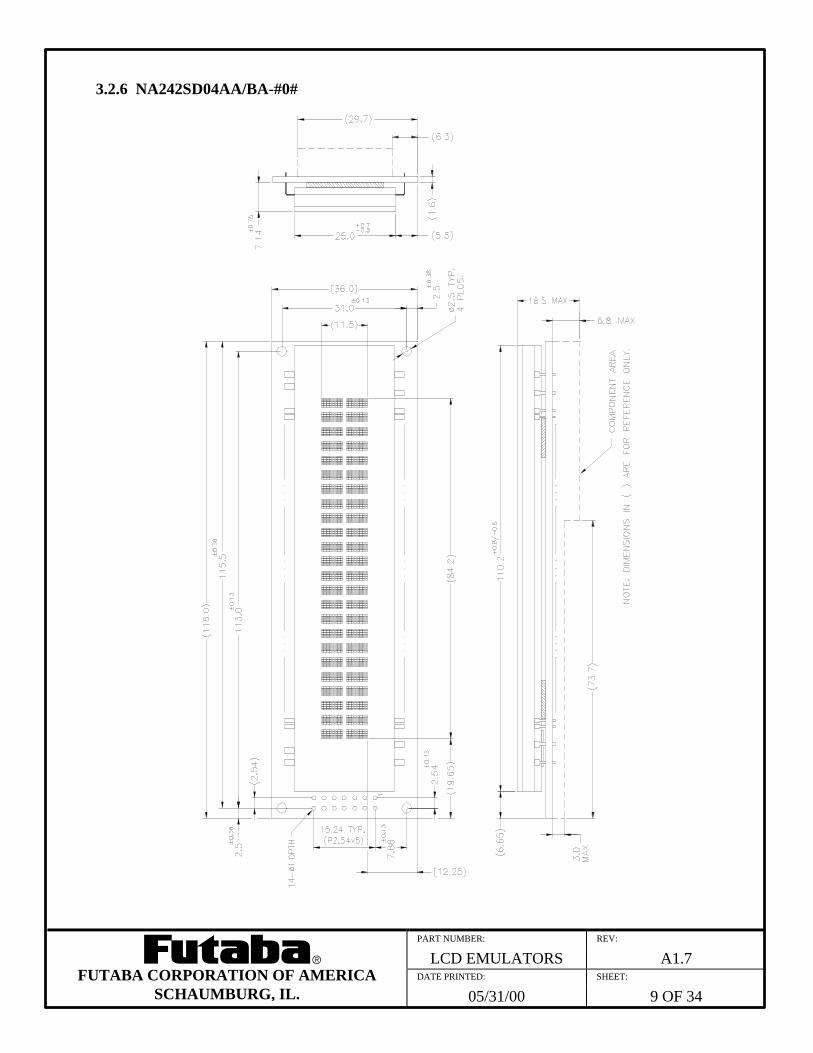
3.2.6 NA242SD04AA/BA-#0#

PART NUMBER: REV:
LCD EMULATORS A1.7DATE PRINTED: SHEET:
05/31/00 10 OF 34FUTABA CORPORATION OF AMERICA
SCHAUMBURG, IL.
3.2.7 NA402SD04AA/BA-#0#

PART NUMBER: REV:
LCD EMULATORS A1.7DATE PRINTED: SHEET:
05/31/00 11 OF 34FUTABA CORPORATION OF AMERICA
SCHAUMBURG, IL.
3.3 SYSTEM BLOCK DIAGRAM
3.4 ENVIRONMENTAL SPECIFICATIONS
Item Symbol Min. Max. Unit CommentOperating temperature Topr -40 +85 oCStorage temperature Tstg -55 +85 oCOperating humidity Hopr 20 85 %RH Without condensationStorage humidity Hstg 20 90 %RH Without condensation
Vibration -- -- 4 G
Total amplitude: 1.5mmFreq: 10 - 55 Hz sine waveSweep time: 1 min./cycleDuration: 2 hrs./axis (X,Y,Z)
Shock -- -- 40 GDuration: 11msWaveform: half sine wave3 times/axis (X,Y,Z,-X,-Y,-Z)
3.5 ABSOLUTE MAXIMUM SPECIFICATIONS
Item Symbol Min. Max. UnitSupply voltage VCC -0.3 6.5 VInput signal voltage VIN -0.3 VCC+0.3 V
FLUORESCENT
DISPLAY
DOT MATRIX
CONTROLLER
VFD
AND DRIVERGRID
DRIVER
VACUUM
DC-DC/ACCONVERTER
NC_RST/_SI/SO
RS_STB
R/W_WR/
E_RD/_SCK
DB0-DB7
Vcc
GND
(IF NEEDED)
(SEE SECTION 2.0)

PART NUMBER: REV:
LCD EMULATORS A1.7DATE PRINTED: SHEET:
05/31/00 12 OF 34FUTABA CORPORATION OF AMERICA
SCHAUMBURG, IL.
3.6 DC ELECTRICAL SPECIFICATIONS
Item Symbol Min. Typ. Max. UnitSupply voltage VCC 4.5 5.0 5.5 V
NA16SD08AA/BA-### - 65 95
NA162SD07AA/BA-### - 120 170
NA202MD15AA/BA-### - 310 440
NA202SD16AA/BA-### - 140 190
NA204SD02AA/BA-### - 300 400
NA242SD04AA/BA-### - 155 215
Supplycurrent
NA402SD10AA/BA-###
ICC
- 220 300
mA
High-level input voltage (see Note)(E,R/W,RD/,SCK,RST/) VIH1 0.8*VCC - VCC V
Low-level input voltage (see Note)(E,R/W,RD/,SCK,RST/) VIL1 0.0 - 0.2*VCC V
High-level input voltage (see Note)(all inputs except E,R/W,RD/,SCK,RST/) VIH2 0.7*VCC - VCC V
Low-level input voltage (see Note)(all inputs except E,R/W,RD/,SCK,RST/) VIL2 0.0 - 0.3*VCC V
High-level output voltage(IOH = -0.1mA) VOH VCC-0.5 - - V
Low-level output voltage(IOL = 0.1mA) VOL - - 0.5 V
Input current (see Note) II -500 - 1.0 uANote: A 10K ohm pull-up resistor is provided on each input for TTL compatibility.
3.7 AC ELECTRICAL SPECIFICATIONS
3.7.1 RESET TIMING
(See Figures 1 and 2)Item Symbol Min. Max. Unit
VCC rise time tRVCC - 10 msVCC off time tOFF 1 - msDelay time after power-up reset tIRSTD 100 - usDelay time after external reset tERSTD 100 - usRST/ pulse width low tRSTL 500 - nsInput signal fall time tf - 15 nsInput signal rise time tr - 15 ns
Note: All timing is specified using 20% and 80% of VCC as the reference points.

PART NUMBER: REV:
LCD EMULATORS A1.7DATE PRINTED: SHEET:
05/31/00 13 OF 34FUTABA CORPORATION OF AMERICA
SCHAUMBURG, IL.
Vcc0.2V
4.5V
tOFF
RS, STB
tIRSTD
tRVCC
Figure 1. Power-up Internal Reset Timing
RST/
tRSTL
RS, STB
tERSTD
tf tr
Figure 2. External Reset Timing
3.7.2 MOTOROLA M68-TYPE PARALLEL INTERFACE TIMING
(See Figures 3 and 4)Item Symbol Min. Max. Unit
RS, R/W setup time tAS 20 - nsRS, R/W hold time tAH 10 - nsInput signal rise time tr - 15 nsInput signal fall time tf - 15 nsE pulse width high PWEH 230 - nsE pulse width low PWEL 230 - nsWrite data setup time tDS 80 - nsWrite data hold time tDH 10 - nsE cycle time tCYCE 500 - nsRead data delay time tDD - 160 nsRead data hold time tDHR 5 - ns
Note: All timing is specified using 20% and 80% of VCC as the reference points.

PART NUMBER: REV:
LCD EMULATORS A1.7DATE PRINTED: SHEET:
05/31/00 14 OF 34FUTABA CORPORATION OF AMERICA
SCHAUMBURG, IL.
R/W
E
DB0-DB7
RS
tAHtAS
PW EH
PWELtDS
tDH
tCYCE
tr tf
Figure 3. Motorola M68-Type Parallel Interface Write Cycle Timing
R/W
E
DB0-DB7
RS
tAHtAS
PW EH
PWEL
tDHR
tCYCE
tr tf
tDD
Figure 4. Motorola M68-Type Parallel Interface Read Cycle Timing
PART NUMBER: REV:
LCD EMULATORS A1.7DATE PRINTED: SHEET:
05/31/00 15 OF 34FUTABA CORPORATION OF AMERICA
SCHAUMBURG, IL.
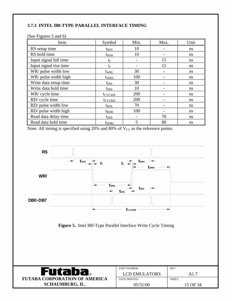
3.7.3 INTEL I80-TYPE PARALLEL INTERFACE TIMING
(See Figures 5 and 6) Item Symbol Min. Max. Unit
RS setup time tRSS 10 - nsRS hold time tRSH 10 - nsInput signal fall time tf - 15 nsInput signal rise time tr - 15 nsWR/ pulse width low tWRL 30 - nsWR/ pulse width high tWRH 100 - nsWrite data setup time tDSi 30 - nsWrite data hold time tDHi 10 - nsWR/ cycle time tCYCWR 200 - nsRD/ cycle time tCYCRD 200 - nsRD/ pulse width low tRDL 70 - nsRD/ pulse width high tRDH 100 - nsRead data delay time tDDi - 70 nsRead data hold time tDHRi 5 80 ns
Note: All timing is specified using 20% and 80% of VCC as the reference points.
RS
WR/
DB0-DB7
tRSS tRSH
tDSi
tCYCWR
tDHitWRL
tWRH
trtf
Figure 5. Intel I80-Type Parallel Interface Write Cycle Timing

PART NUMBER: REV:
LCD EMULATORS A1.7DATE PRINTED: SHEET:
05/31/00 16 OF 34FUTABA CORPORATION OF AMERICA
SCHAUMBURG, IL.
RS
RD/
DB0-DB7
tRSS tftRSHtr
tRDL
tRDH
tDHRi
tCYCRD
tDDi
Figure 6. Intel I80-Type Parallel Interface Read Cycle Timing
3.7.4 SYNCHRONOUS SERIAL INTERFACE TIMING
(See Figures 7, 8 and 12)Item Symbol Min. Max. Unit
STB setup time tSTBS 100 - nsSTB hold time tSTBH 500 - nsInput signal fall time tf - 15 nsInput signal rise time tr - 15 nsSTB pulse width high tWSTB 500 - nsSCK pulse width high tSCKH 200 - nsSCK pulse width low tSCKL 200 - nsSI data setup time tDSs 100 - nsSI data hold time tDHs 100 - nsSCK cycle time tCYCSCK 500 - nsSCK wait time between bytes tWAIT 1 - usSO data delay time tDDs - 150 nsSO data hold time tDHRs 5 - ns
Note: All timing is specified using 20% and 80% of VCC as the reference points.

PART NUMBER: REV:
LCD EMULATORS A1.7DATE PRINTED: SHEET:
05/31/00 17 OF 34FUTABA CORPORATION OF AMERICA
SCHAUMBURG, IL.
STB
SCK
SI/SO
tDSstDHs
tSCKL
tSCKH
tCYCSCKtSTBS tSTBH
tWSTB
trtf
Figure 7. Synchronous Serial Interface Write Cycle Timing
STB
SCK
SI/SO
tDHRstSCKL
tSCKH
tCYCSCKtSTBS tSTBH
tWSTB
trtf
tDDs
Figure 8. Synchronous Serial Interface Read Cycle Timing

PART NUMBER: REV:
LCD EMULATORS A1.7DATE PRINTED: SHEET:
05/31/00 18 OF 34FUTABA CORPORATION OF AMERICA
SCHAUMBURG, IL.
4.0 MODES OF OPERATION
The following modes of operation are selectable via jumpers (see section 8.0 Jumper Settings).
4.1 PARALLEL INTERFACE MODES
In the parallel interface mode, 8-bit instructions and data are sent between the host and themodules using either 4-bit nibbles or 8-bit bytes. Nibbles are transmitted high nibble first onDB4-DB7 (DB0-DB3 are ignored) whereas bytes are transmitted on DB0-DB7. The RegisterSelect (RS) control signal is used to identify DB0-DB7 as an instruction (low) or data (high).
4.1.1 MOTOROLA M68-TYPE MODE
This mode uses the Read/Write (R/W) and Enable (E) control signals to transfer information.Instructions/data are written to the modules on the falling edge of E when R/W is low and areread from the modules after the rising edge of E when R/W is high.
R/W
E
DB7 IB3IB7 IB7 IB3 BF= '0' IB3 DB7 DB3
IB6 IB2 IB6 IB2 IB2IB6 DB6 DB2DB6
IB5 IB1 IB5 IB1 IB1IB5 DB5 DB1DB5
IB4 IB0 IB4 IB0 IB0IB4 DB4 DB0DB4
Write instruction Write instruction Read instruction Write data
RS
Figure 9. Typical 4-Bit Parallel Interface Sequence Using M68-Type Mode

PART NUMBER: REV:
LCD EMULATORS A1.7DATE PRINTED: SHEET:
05/31/00 19 OF 34FUTABA CORPORATION OF AMERICA
SCHAUMBURG, IL.
4.1.2 INTEL I80-TYPE MODE
This mode uses the Read (RD/) and Write (WR/) control signals to transfer information.Instructions/data are written to the modules on the rising edge of WR/ and are read from themodules after the falling edge of RD/.
WR/
RD/
DB7 IB7 IB7 BF= '0' DB7
IB6 IB6 IB6 DB6DB6
IB0 IB0 IB0 DB0DB0
Write instruction Write instruction Read instruction Write data
RS
Figure 10. Typical 8-Bit Parallel Interface Sequence Using I80-Type Mode
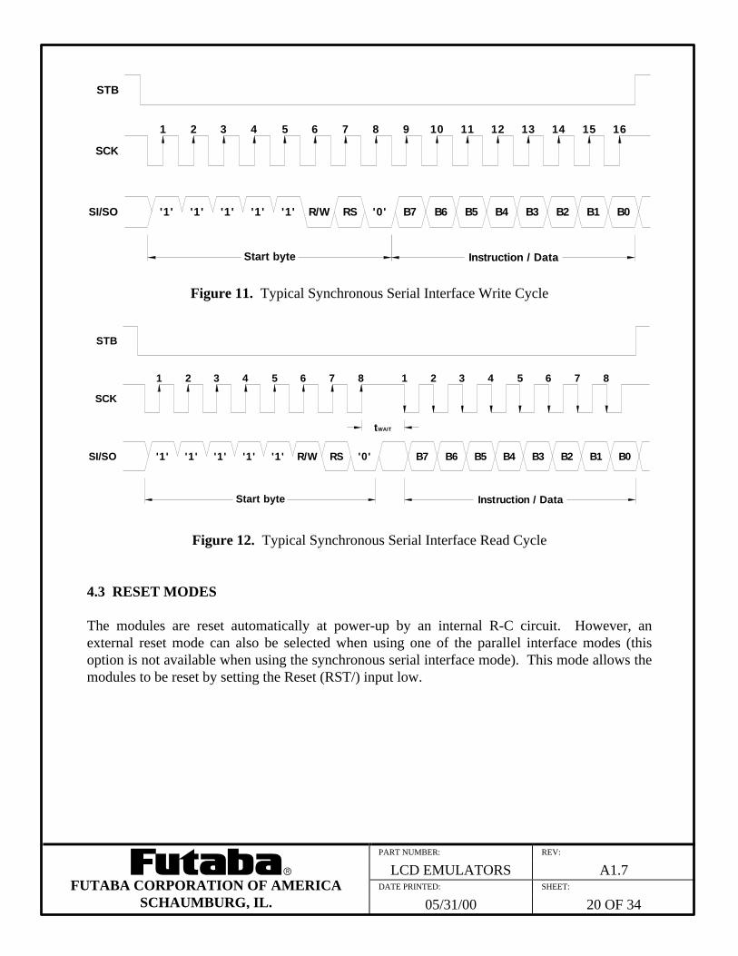
4.2 SYNCHRONOUS SERIAL INTERFACE MODE
In the synchronous serial interface mode, instructions and data are sent between the host and themodules using 8-bit bytes. Two bytes are required per read/write cycle and are transmitted MSBfirst. The start byte contains 5 high bits, the Read/Write (R/W) control bit, the Register Select(RS) control bit, and a low bit. The following byte contains the instruction/data bits. The R/Wbit determines whether the cycle is a read (high) or a write (low) cycle. The RS bit is used toidentify the second byte as an instruction (low) or data (high).
This mode uses the Strobe (STB) control signal, Serial Clock (SCK) input, and Serial I/O(SI/SO) line to transfer information. In a write cycle, bits are clocked into the modules on therising edge of SCK. In a read cycle, bits in the start byte are clocked into the modules on therising edge of SCK. After the minimum wait time, each bit in the instruction/data byte can beread from the modules after each falling edge of SCK. Each read/write cycle begins on thefalling edge of STB and ends on the rising edge. To be a valid read/write cycle, the STB must gohigh at the end of the cycle.
PART NUMBER: REV:
LCD EMULATORS A1.7DATE PRINTED: SHEET:
05/31/00 20 OF 34FUTABA CORPORATION OF AMERICA
SCHAUMBURG, IL.
STB
SCK
SI/SO
1 2 3 4 5 6 7 8 9 10 11 12 13 14 15 16
B0B1B2B3B4B5B6B7'0'RSR/W'1''1''1''1''1'
Start byte Instruction / Data
Figure 11. Typical Synchronous Serial Interface Write Cycle
STB
SCK
SI/SO
1 2 3 4 5 6 7 8 1 2 3 4 5 6 7 8
B0B1B2B3B4B5B6'0'RSR/W'1''1''1''1''1'
Start byte Instruction / Data
tWAIT
B7
Figure 12. Typical Synchronous Serial Interface Read Cycle
4.3 RESET MODES
The modules are reset automatically at power-up by an internal R-C circuit. However, anexternal reset mode can also be selected when using one of the parallel interface modes (thisoption is not available when using the synchronous serial interface mode). This mode allows themodules to be reset by setting the Reset (RST/) input low.

PART NUMBER: REV:
LCD EMULATORS A1.7DATE PRINTED: SHEET:
05/31/00 21 OF 34FUTABA CORPORATION OF AMERICA
SCHAUMBURG, IL.
5.0 CHARACTER FONT TABLES
5.1 ENGLISH / KATAKANA CHARACTER FONT (Option A)
1111
1110
1101
1100
1011
1010
1001
1000
0111
0110
0101
0100
0011
0010
0001
0000
CGRAM(8)
CGRAM(7)
CGRAM(6)
CGRAM(5)
CGRAM(4)
CGRAM(3)
CGRAM(2)
CGRAM(1)
CGRAM(8)
CGRAM(7)
CGRAM(6)
CGRAM(5)
CGRAM(4)
CGRAM(3)
CGRAM(2)
CGRAM(1)
0000 0001 0010 0011 0100 0101 0110 0111 1000 1001 1010 1011 1100 1101 1110 1111
UPPERNIBBLE
LOWERNIBBLE

PART NUMBER: REV:
LCD EMULATORS A1.7DATE PRINTED: SHEET:
05/31/00 22 OF 34FUTABA CORPORATION OF AMERICA
SCHAUMBURG, IL.
5.2 ENGLISH / EUROPEAN CHARACTER FONT (Option B)
1111
1110
1101
1100
1011
1010
1001
1000
0111
0110
0101
0100
0011
0010
0001
0000
CGRAM(8)
CGRAM(7)
CGRAM(6)
CGRAM(5)
CGRAM(4)
CGRAM(3)
CGRAM(2)
CGRAM(1)
CGRAM(8)
CGRAM(7)
CGRAM(6)
CGRAM(5)
CGRAM(4)
CGRAM(3)
CGRAM(2)
CGRAM(1)
0000 0001 0010 0011 0100 0101 0110 0111 1000 1001 1010 1011 1100 1101 1110 1111
UPPERNIBBLE
LOWERNIBBLE

PART NUMBER: REV:
LCD EMULATORS A1.7DATE PRINTED: SHEET:
05/31/00 23 OF 34FUTABA CORPORATION OF AMERICA
SCHAUMBURG, IL.
6.0 FUNCTIONAL DESCRIPTION
6.1 ADDRESS COUNTER (AC)
6.1.1 SINGLE LINE DISPLAYSThe AC stores the address of the data being written to and read from DDRAM or CGRAM. TheAC increments by 1 (overflows from 4FH to 00H) or decrements by 1 (underflows from 00H to4FH) after each DDRAM access. The AC increments by 1 (overflows from 3FH to 00H) ordecrements by 1 (underflows from 00H to 3FH) after each CGRAM access. When addressingDDRAM, the value in the AC also represents the cursor position.
6.1.2 MULTIPLE LINE DISPLAYSThe AC stores the address of the data being written to and read from DDRAM or CGRAM. TheAC increments by 1 (overflows from 27H to 40H and from 67H to 00H) or decrements by 1(underflows from 40H to 27H and from 00H to 67H) after each DDRAM access. The ACincrements by 1 (overflows from 3FH to 00H) or decrements by 1 (underflows from 00H to 3FH)after each CGRAM access. When addressing DDRAM, the value in the AC also represents thecursor position.
6.2 DISPLAY DATA RAM (DDRAM)
6.2.1 SINGLE LINE DISPLAYSThe DDRAM stores the character code of each character being displayed on the VFD. ValidDDRAM addresses are 00H to 4FH. DDRAM not being used for display characters can be usedas general purpose RAM. The tables below show the relationship between the DDRAM addressand the character position on the VFD before and after a display shift (with the number of displaylines set to 1).
6.2.2 MULTIPLE LINE DISPLAYSThe DDRAM stores the character code of each character being displayed on the VFD. ValidDDRAM addresses are 00H to 27H and 40H to 67H. DDRAM not being used for displaycharacters can be used as general purpose RAM. The tables below show the relationshipbetween the DDRAM address and the character position on the VFD before and after a displayshift (with the number of display lines set to 2).

PART NUMBER: REV:
LCD EMULATORS A1.7DATE PRINTED: SHEET:
05/31/00 24 OF 34FUTABA CORPORATION OF AMERICA
SCHAUMBURG, IL.
6.3 DISPLAY SHIFT DETAIL
6.3.1 NA16SD08AA/BA-###Relationship before a display shift (non-shifted):
1 2 3 4 5 6 7 8 9 10 11 12 13 14 15 161 00 01 02 03 04 05 06 07 08 09 0A 0B 0C 0D 0E 0F
Relationship after a display shift to the left:
1 2 3 4 5 6 7 8 9 10 11 12 13 14 15 161 01 02 03 04 05 06 07 08 09 0A 0B 0C 0D 0E 0F 10
Relationship after a display shift to the right:
1 2 3 4 5 6 7 8 9 10 11 12 13 14 15 161 4F 00 01 02 03 04 05 06 07 08 09 0A 0B 0C 0D 0E
6.3.2 NA162SD08AA/BA-###Relationship before a display shift (non-shifted):
1 2 3 4 5 6 7 8 9 10 11 12 13 14 15 161 00 01 02 03 04 05 06 07 08 09 0A 0B 0C 0D 0E 0F2 40 41 42 43 44 45 46 47 48 49 4A 4B 4C 4D 4E 4F
Relationship after a display shift to the left:
1 2 3 4 5 6 7 8 9 10 11 12 13 14 15 161 01 02 03 04 05 06 07 08 09 0A 0B 0C 0D 0E 0F 102 41 42 43 44 45 46 47 48 49 4A 4B 4C 4D 4E 4F 50
Relationship after a display shift to the right:
1 2 3 4 5 6 7 8 9 10 11 12 13 14 15 161 27 00 01 02 03 04 05 06 07 08 09 0A 0B 0C 0D 0E2 67 40 41 42 43 44 45 46 47 48 49 4A 4B 4C 4D 4E

PART NUMBER: REV:
LCD EMULATORS A1.7DATE PRINTED: SHEET:
05/31/00 25 OF 34FUTABA CORPORATION OF AMERICA
SCHAUMBURG, IL.
6.3.3 NA202MD15AA/BA-### AND NA202SD16AA/BA-###Relationship before a display shift (non-shifted):
1 2 3 4 5 6 7 8 9 10 11 12 13 14 15 16 17 18 19 201 00 01 02 03 04 05 06 07 08 09 0A 0B 0C 0D 0E 0F 10 11 12 132 40 41 42 43 44 45 46 47 48 49 4A 4B 4C 4D 4E 4F 50 51 52 53
Relationship after a display shift to the left:
1 2 3 4 5 6 7 8 9 10 11 12 13 14 15 16 17 18 19 201 01 02 03 04 05 06 07 08 09 0A 0B 0C 0D 0E 0F 10 11 12 13 142 41 42 43 44 45 46 47 48 49 4A 4B 4C 4D 4E 4F 50 51 52 53 54
Relationship after a display shift to the right:
1 2 3 4 5 6 7 8 9 10 11 12 13 14 15 16 17 18 19 201 27 00 01 02 03 04 05 06 07 08 09 0A 0B 0C 0D 0E 0F 10 11 122 67 40 41 42 43 44 45 46 47 48 49 4A 4B 4C 4D 4E 4F 50 51 52
6.3.4 NA204SD02AA/BA-###Relationship before a display shift (non-shifted):
1 2 3 4 5 6 7 8 9 10 11 12 13 14 15 16 17 18 19 201 00 01 02 03 04 05 06 07 08 09 0A 0B 0C 0D 0E 0F 10 11 12 132 40 41 42 43 44 45 46 47 48 49 4A 4B 4C 4D 4E 4F 50 51 52 533 14 15 16 17 18 19 1A 1B 1C 1D 1E 1F 20 21 22 23 24 25 26 274 54 55 56 57 58 59 5A 5B 5C 5D 5E 5F 60 61 62 63 64 65 66 67
Relationship after a display shift to the left:
1 2 3 4 5 6 7 8 9 10 11 12 13 14 15 16 17 18 19 201 01 02 03 04 05 06 07 08 09 0A 0B 0C 0D 0E 0F 10 11 12 13 142 41 42 43 44 45 46 47 48 49 4A 4B 4C 4D 4E 4F 50 51 52 53 543 15 16 17 18 19 1A 1B 1C 1D 1E 1F 20 21 22 23 24 25 26 27 004 55 56 57 58 59 5A 5B 5C 5D 5E 5F 60 61 62 63 64 65 66 67 40
Relationship after a display shift to the right:
1 2 3 4 5 6 7 8 9 10 11 12 13 14 15 16 17 18 19 201 27 00 01 02 03 04 05 06 07 08 09 0A 0B 0C 0D 0E 0F 10 11 122 67 40 41 42 43 44 45 46 47 48 49 4A 4B 4C 4D 4E 4F 50 51 523 13 14 15 16 17 18 19 1A 1B 1C 1D 1E 1F 20 21 22 23 24 25 264 53 54 55 56 57 58 59 5A 5B 5C 5D 5E 5F 60 61 62 63 64 65 66
PART NUMBER: REV:
LCD EMULATORS A1.7DATE PRINTED: SHEET:
05/31/00 26 OF 34FUTABA CORPORATION OF AMERICA
SCHAUMBURG, IL.
6.3.5 NA242SD04AA/BA-###Relationship before a display shift (non-shifted):
1 2 3 4 5 6 7 8 9 10 11 12 13 14 15 16 17 18 19 20 21 22 23 241 00 01 02 03 04 05 06 07 08 09 0A 0B 0C 0D 0E 0F 10 11 12 13 14 15 16 172 40 41 42 43 44 45 46 47 48 49 4A 4B 4C 4D 4E 4F 50 51 52 53 54 55 56 57
Relationship after a display shift to the left:
1 2 3 4 5 6 7 8 9 10 11 12 13 14 15 16 17 18 19 20 21 22 23 241 01 02 03 04 05 06 07 08 09 0A 0B 0C 0D 0E 0F 10 11 12 13 14 15 16 17 182 41 42 43 44 45 46 47 48 49 4A 4B 4C 4D 4E 4F 50 51 52 53 54 55 56 57 58
Relationship after a display shift to the right:
1 2 3 4 5 6 7 8 9 10 11 12 13 14 15 16 17 18 19 20 21 22 23 241 27 00 01 02 03 04 05 06 07 08 09 0A 0B 0C 0D 0E 0F 10 11 12 13 14 15 162 67 40 41 42 43 44 45 46 47 48 49 4A 4B 4C 4D 4E 4F 50 51 52 53 54 55 56
6.3.6 NA402SD10AA/BA-###Relationship before a display shift (non-shifted):
1 2 3 4 5 6 7 8 9 32 33 34 35 36 37 38 39 401 00 01 02 03 04 05 06 07 08 - - - - - 1F 20 21 22 23 24 25 26 272 40 41 42 43 44 45 46 47 48 - - - - - 5F 60 61 62 63 64 65 66 67
Relationship after a display shift to the left:
1 2 3 4 5 6 7 8 9 32 33 34 35 36 37 38 39 401 01 02 03 04 05 06 07 08 09 - - - - - 20 21 22 23 24 25 26 27 002 41 42 43 44 45 46 47 48 49 - - - - - 60 61 62 63 64 65 66 67 40
Relationship after a display shift to the right:
1 2 3 4 5 6 7 8 9 32 33 34 35 36 37 38 39 401 27 00 01 02 03 04 05 06 07 - - - - - 1E 1F 20 21 22 23 24 25 262 67 40 41 42 43 44 45 46 47 - - - - - 5E 5F 60 61 62 63 64 65 66

PART NUMBER: REV:
LCD EMULATORS A1.7DATE PRINTED: SHEET:
05/31/00 27 OF 34FUTABA CORPORATION OF AMERICA
SCHAUMBURG, IL.
6.4 CHARACTER GENERATOR RAM (CGRAM)
The CGRAM stores the pixel information (1 = pixel on, 0 = pixel off) for the eight user-definable 5x8 characters. Valid CGRAM addresses are 00H to 3FH. CGRAM not being used todefine characters can be used as general purpose RAM (lower 5 bits only). Character codes 00Hto 07H (or 08H to 0FH) are assigned to the user-definable characters (see section 5.0 CharacterFont Tables). The table below shows the relationship between the character codes, CGRAMaddresses, and CGRAM data for each user-definable character.
D7 D3D4D5D6 D1D2 D0 A3A4A5 A0A1A2 D3D4D5D6D7 D0D1D2X0000 000 X X X
Character code CGRAM address CGRAM data
00 00000 0 10 1 00 1 11 0 01 0 11 1 01 1 1
0 0000 0000 000
00 0000 0000 000
X0 0 0 0 0 0 1 0
1111
11
11
00
00
001 0 00
1
1
1
1
0
0
0
0 X
0
0XX
00 000 0 000 0 000 0 000 0 000 00
0
00
1X0000 111 1 0010 000
00
11
111 11 1
X XX0
0
0
0
1
1
1
1
0 0000
0 000 000 00
0 000 00
(1)CGRAM
(2)CGRAM
(8)CGRAM
111111111 1 1 1111
1111
111111
1 1 11
11 1
111111
111111
1 1 1
x = don't care
6.5 INSTRUCTIONS
Instruction RS R/W DB7 DB6 DB5 DB4 DB3 DB2 DB1 DB0Clear display 0 0 0 0 0 0 0 0 0 1Cursor home 0 0 0 0 0 0 0 0 1 xEntry mode set 0 0 0 0 0 0 0 1 I/D SDisplay on/off control 0 0 0 0 0 0 1 D C BCursor/display shift 0 0 0 0 0 1 S/C R/L x xFunction set 0 0 0 0 1 DL N x BR1 BR0CGRAM address set 0 0 0 1 CGRAM addressDDRAM address set 0 0 1 DDRAM addressAddress counter read 0 1 BF=0 AC contentsDDRAM or CGRAM write 1 0 Write dataDDRAM or CGRAM read 1 1 Read data
x = don’t care

PART NUMBER: REV:
LCD EMULATORS A1.7DATE PRINTED: SHEET:
05/31/00 28 OF 34FUTABA CORPORATION OF AMERICA
SCHAUMBURG, IL.
6.5.1 CLEAR DISPLAY
RS R/W DB7 DB6 DB5 DB4 DB3 DB2 DB1 DB00 0 0 0 0 0 0 0 0 1
This instruction clears the display (without affecting the contents of CGRAM) by performing thefollowing:
1) Fills all DDRAM locations with character code 20H (character code for a space).2) Sets the AC to DDRAM address 00H (i.e. sets cursor position to 00H).3) Returns the display to the non-shifted position.4) Sets the I/D bit to 1.
6.5.2 CURSOR HOME
RS R/W DB7 DB6 DB5 DB4 DB3 DB2 DB1 DB00 0 0 0 0 0 0 0 1 x
x = don’t care
This instruction returns the cursor to the home position (without affecting the contents ofDDRAM or CGRAM) by performing the following:
1) Sets the AC to DDRAM address 00H (i.e. sets cursor position to 00H).2) Returns the display to the non-shifted position.
6.5.3 ENTRY MODE SET
RS R/W DB7 DB6 DB5 DB4 DB3 DB2 DB1 DB00 0 0 0 0 0 0 1 I/D S
This instruction selects whether the AC (cursor position) increments or decrements after eachDDRAM or CGRAM access and determines the direction the information on the display shiftsafter each DDRAM write. The instruction also enables or disables display shifts after eachDDRAM write (information on the display does not shift after a DDRAM read or CGRAMaccess). DDRAM, CGRAM, and AC contents are not affected by this instruction.
I/D = 0: The AC decrements after each DDRAM or CGRAM access. If S = 1, the informationon the display shifts to the right by one character position after each DDRAM write.
I/D = 1: The AC increments after each DDRAM or CGRAM access. If S = 1, the informationon the display shifts to the left by one character position after each DDRAM write.
S = 0: The display shift function is disabled.S = 1: The display shift function is enabled.

PART NUMBER: REV:
LCD EMULATORS A1.7DATE PRINTED: SHEET:
05/31/00 29 OF 34FUTABA CORPORATION OF AMERICA
SCHAUMBURG, IL.
6.5.4 DISPLAY ON/OFF CONTROL
RS R/W DB7 DB6 DB5 DB4 DB3 DB2 DB1 DB00 0 0 0 0 0 1 D C B
This instruction selects whether the display and cursor are on or off and selects whether or notthe character at the current cursor position blinks. DDRAM, CGRAM, and AC contents are notaffected by this instruction.
D = 0: The display is off (display blank).D = 1: The display is on (contents of DDRAM displayed).
C = 0: The cursor is off.C = 1: The cursor is on (8th row of pixels).
B = 0: The blinking character function is disabled.B = 1: The blinking character function is enabled (a character with all pixels on will alternate
with the character displayed at the current cursor position at about a 1Hz rate with a50% duty cycle).
6.5.5 CURSOR/DISPLAY SHIFT
RS R/W DB7 DB6 DB5 DB4 DB3 DB2 DB1 DB00 0 0 0 0 1 S/C R/L x x
x = don’t care
This instruction increments or decrements the AC (cursor position) and shifts the information onthe display one character position to the left or right without accessing DDRAM or CGRAM.DDRAM and CGRAM contents are not affected by this instruction. If the AC was addressingCGRAM prior to this instruction, the AC will be addressing DDRAM after this instruction.However, if the AC was addressing DDRAM prior to this instruction, the AC will still beaddressing DDRAM after this instruction.
S/C R/L AC contents (cursor position) Information on the display0 0 Decrements by one No change0 1 Increments by one No change1 0 Decrements by one Shifts one character position to the left1 1 Increments by one Shifts one character position to the right

PART NUMBER: REV:
LCD EMULATORS A1.7DATE PRINTED: SHEET:
05/31/00 30 OF 34FUTABA CORPORATION OF AMERICA
SCHAUMBURG, IL.
6.5.6 FUNCTION SET
RS R/W DB7 DB6 DB5 DB4 DB3 DB2 DB1 DB00 0 0 0 1 DL N x BR1 BR0
x = don’t care
This instruction sets the width of the data bus for the parallel interface modes, the number ofdisplay lines, and the luminance level (brightness) of the VFD. It must be the first command sentafter any reset. DDRAM, CGRAM, and AC contents are not affected by this instruction.
DL = 0: Sets the data bus width for the parallel interface modes to 4-bit (DB7-DB4).DL = 1: Sets the data bus width for the parallel interface modes to 8-bit (DB7-DB0).
N = 0: Sets the number of display lines to 1 (this setting is not recommended for multiple linedisplays).
N = 1: Sets the number of display lines to 2 (this setting is not recommended for single linedisplays).
BR1,BR0 = 0,0: Sets the luminance level to 100%. 0,1: Sets the luminance level to 75%. 1,0: Sets the luminance level to 50%. 1,1: Sets the luminance level to 25%.
6.5.7 CGRAM ADDRESS SET
RS R/W DB7 DB6 DB5 DB4 DB3 DB2 DB1 DB00 0 0 1 CGRAM address
This instruction places the 6-bit CGRAM address specified by DB5-DB0 into the AC (cursorposition). Subsequent data writes (reads) will be to (from) CGRAM. DDRAM and CGRAMcontents are not affected by this instruction.
6.5.8 DDRAM ADDRESS SET
RS R/W DB7 DB6 DB5 DB4 DB3 DB2 DB1 DB00 0 1 DDRAM address
This instruction places the 7-bit DDRAM address specified by DB6-DB0 into the AC (cursorposition). Subsequent data writes (reads) will be to (from) DDRAM. DDRAM and CGRAMcontents are not affected by this instruction.

PART NUMBER: REV:
LCD EMULATORS A1.7DATE PRINTED: SHEET:
05/31/00 31 OF 34FUTABA CORPORATION OF AMERICA
SCHAUMBURG, IL.
6.5.9 ADDRESS COUNTER READ
RS R/W DB7 DB6 DB5 DB4 DB3 DB2 DB1 DB00 1 BF=0 AC contents
This instruction reads the current 7-bit address from the AC on DB6-DB0 and the busy flag (BF)bit (always 0) on DB7. DDRAM, CGRAM, and AC contents are not affected by this instruction.Because the BF is always 0, the host never has to read the BF bit to determine if the modules arebusy before sending data or instructions. Therefore, data and instructions can be sent to themodules continuously according to the E, WR/, and SCK cycle times specified in section 3.7 ACTiming Specifications. Due to this feature, the execution times for each instruction are notspecified.
6.5.10 DDRAM OR CGRAM WRITE
RS R/W DB7 DB6 DB5 DB4 DB3 DB2 DB1 DB01 0 Write data
This instruction writes the 8-bit data byte on DB7-DB0 into the DDRAM or CGRAM locationaddressed by the AC. The most recent DDRAM or CGRAM Address Set instruction determineswhether the write is to DDRAM or CGRAM. This instruction also increments or decrements theAC and shifts the display according to the I/D and S bits set by the Entry Mode Set instruction.
6.5.11 DDRAM OR CGRAM READ
RS R/W DB7 DB6 DB5 DB4 DB3 DB2 DB1 DB01 1 Read data
This instruction reads the 8-bit data byte from the DDRAM or CGRAM location addressed bythe AC on DB7-DB0. The most recent DDRAM or CGRAM Address Set instruction determineswhether the read is from DDRAM or CGRAM. This instruction also increments or decrementsthe AC and shifts the display according to the I/D and S bits set by the Entry Mode Setinstruction. Before sending this instruction, a DDRAM or CGRAM Address Set instructionshould be executed to set the AC to the desired DDRAM or CGRAM address to be read.

PART NUMBER: REV:
LCD EMULATORS A1.7DATE PRINTED: SHEET:
05/31/00 32 OF 34FUTABA CORPORATION OF AMERICA
SCHAUMBURG, IL.
6.6 RESET CONDITIONS
After either a power-up reset or an external reset, the modules initialize to the followingconditions:
1) All DDRAM locations are set to 20H (character code for a space).2) The AC is set to DDRAM address 00H (i.e. sets cursor position to 00H).3) The relationship between DDRAM addresses and character positions on the VFD is set to the
non-shifted position.4) Entry Mode Set instruction bits:
I/D = 1: The AC increments after each DDRAM or CGRAM access.S = 0: The display shift function is disabled.
5) Display On/Off Control instruction bits:D = 0: The display is off (display blank).C = 0: The cursor is off.B = 0: The blinking character function is disabled.
6) Function Set instruction bits:DL = 1: Sets the data bus width for the parallel interface modes to 8-bit (DB7-DB0).N = 1(0): Number of display lines set to 2 for multiple line displays (number of display
lines set to 1 for single line displays).BR1,BR0 = 0,0: Sets the luminance level to 100%.
Note that the function set command must be the first instruction sent to the module after anyreset.
6.6.1 INITIALIZATION
The modules can be initialized by using instructions if the modules are not reset according to thereset timing detailed in Section 3.7.1 (Reset Timing). After any reset, the function set commandmust be the first instruction sent to the module.

PART NUMBER: REV:
LCD EMULATORS A1.7DATE PRINTED: SHEET:
05/31/00 33 OF 34FUTABA CORPORATION OF AMERICA
SCHAUMBURG, IL.
7.0 CONNECTOR INTERFACE
PinNo.
Serial Parallel(Intel)
Parallel(Motorola)
PinNo.
Serial Parallel(Intel)
Parallel(Motorola)
1 GND GND GND 2 VCC VCC VCC
3 SI/SO NC or RST/ NC or RST/ 4 STB RS RS5 NC WR/ R/W 6 SCK RD/ E7 NC DB0 DB0 8 NC DB1 DB19 NC DB2 DB2 10 NC DB3 DB311 NC DB4 DB4 12 NC DB5 DB513 NC DB6 DB6 14 NC DB7 DB715* NC NC NC 16* NC NC NC
NC = No Connection*If applicable.
7.1 CONNECTOR CONFIGURATION
Product Number Connector (if applicable) Configuration
NA16SD08AA/BA-#1# Amp P/N 1-103747-5 or equivalent 1 x 15
NA162SD07AA/BA-#1# Amp P/N 1-103747-4 or equivalent 1 x 14
NA202MD15AA/BA-#1#* Berg P/N 67997-114 or equivalent 2 x 7
NA202SD16AA/BA-#1# Berg P/N 67997-114 or equivalent 2 x 7
NA204SD02AA/BA-#1# Amp P/N 1-103747-6 or equivalent 1 x 16
NA242SD04AA/BA-#1# Berg P/N 67997-114 or equivalent 2 x 7
NA402SD10AA/BA-#1# Berg P/N 67997-114 or equivalent 2 x 7
*Also has holes that accept a 1 x 16 connector, Amp P/N 1-103747-6 or equivalent.

PART NUMBER: REV:
LCD EMULATORS A1.7DATE PRINTED: SHEET:
05/31/00 34 OF 34FUTABA CORPORATION OF AMERICA
SCHAUMBURG, IL.
8.0 JUMPER SETTINGS
Mode JP2 JP3 JP4 JP5 JP6 JP7Parallel (Motorola) (Note 1) open shorted open shorted openParallel (Intel) (Note 1) open shorted open open shortedSerial open shorted open shorted shorted open
Note 1: JP2 shorted (open) enables (disables) external reset mode.
9.0 PART NUMBER OPTIONS
NA202SD16BA - 0 0 1
0: Internal R-C reset1: External reset
0: Without connector1: With straight pin header connector mounted on component side#: Customer specified connector - Contact Futaba for this option
0: Motorola M68-type parallel interface1: Intel I80-type parallel interface2: Serial type interface
Sequential revision letter (see revision tables for current letter)
A: English - Katakana character fontB: English - European character font
This example defines a 20 x 2 LCD Emulator display with English - European character font,revision letter A, Motorola M68-type interface, no connector, and external reset.


![P1043 Code revision 2016 AppR - Food Standards Australia ... Web view20 February 2017 [06–17] Approval report – Proposal P1043. Code Revision (2016) Food Standards Australia New](https://static.fdocuments.in/doc/165x107/5ab771ad7f8b9ad13d8b5db8/p1043-code-revision-2016-appr-food-standards-australia-web-view20-february.jpg)