Results and prospective of CVD processing with … · Web viewRaman measurements were carried out...
34
RESULTS AND PROSPECTIVE OF CVD PROCESSING WITH USE OF COMPLICATED ELEMENTORGANIC COMPOUNDS IN PREPARATION OF ELECTRONIC MATERIALS F.A. Kuznetsov, I.K. Igumenov, T.P. Smirnova, N.I. Fainer, N.V. Gelfond, M.L. Kosinova, N.B. Morozova, Yu. M. Rumyantsev, L.V. Yakovkina Nikolaev Institute of Inorganic Chemistry SB RAS, Novosibirsk, Russia Abstract Chemical vapour deposition were used to produced high k dielectric films of HfO 2 films, low k dielectric films of SiC x N y and metal films of platinum group metals. IR and Raman spectroscopy, AES, XPS, ellipsometry, XRD using the synchrotron radiation, EDS, SEM, AFM, measurements of electrophysical, mechanical characteristics and optical properties were applied to study their physicochemical and functional properties.HfO 2 films were grown on n-type Si(100) substrates using dipivaloilmethanate hafnium (IV) and cyclopentadienyl hafnium bisdiethylamide as precursors. It was found that the deposited HfO 2 films react with the SiO 2 layer to be synthesized on silicon substrate and an intermediate amorphous layer was formed. The amorphous layer is composed of hafnium silicate and nonreacted SiO 2 layer. It was shown by thermodynamic analysis of the Si-SiO 2 -HfO 2 -Hf system that a composition Si/HfO 2-у is thermodynamically stable into narrow interval of oxygen pressure. As the oxygen partial pressure was increased (which is equivalent to presence of SiO 2 layer) the composition Si/HfSiO 4 /HfO 2-у is equilibrium. SiC x N y films were synthesized using siliconorganic compound as single-source precursor. It was shown that low temperature films are low-k dielectrics with the following characteristics: a dielectric constant of 3.0 – 7.0, specific resistance, = 10 13 -10 16 Omcm, E dielectric breakdown ~ 1 MV/cm, surface state density N ss ~ 2.4·10 11 cm -2 ·eV -1 and fixed charge density of about 1.6 x 10 11 cm -2 . The bandgap of the films changes from 5.35 up to ~ 3.30 eV. Microhardness of these films changes from 1.9 up to 2.4 28
Transcript of Results and prospective of CVD processing with … · Web viewRaman measurements were carried out...
RESULTS AND PROSPECTIVE OF CVD PROCESSING WITH USE OF COMPLICATED ELEMENTORGANIC COMPOUNDS IN PREPARATION OF ELECTRONIC
MATERIALS
F.A. Kuznetsov, I.K. Igumenov, T.P. Smirnova, N.I. Fainer, N.V. Gelfond,M.L. Kosinova, N.B. Morozova, Yu. M. Rumyantsev, L.V. Yakovkina
Nikolaev Institute of Inorganic Chemistry SB RAS, Novosibirsk, Russia
Abstract
Chemical vapour deposition were used to produced high k dielectric films of HfO2 films, low k dielectric films of SiCxNy and metal films of platinum group metals. IR and Raman spectroscopy, AES, XPS, ellipsometry, XRD using the synchrotron ra-diation, EDS, SEM, AFM, measurements of electrophysical, mechanical characteris-tics and optical properties were applied to study their physicochemical and functional properties.HfO2 films were grown on n-type Si(100) substrates using dipivaloil-methanate hafnium (IV) and cyclopentadienyl hafnium bisdiethylamide as precursors. It was found that the deposited HfO2 films react with the SiO2 layer to be synthesized on silicon substrate and an intermediate amorphous layer was formed. The amorphous layer is composed of hafnium silicate and nonreacted SiO2 layer. It was shown by thermodynamic analysis of the Si-SiO2-HfO2-Hf system that a composition Si/HfO2-у
is thermodynamically stable into narrow interval of oxygen pressure. As the oxygen partial pressure was increased (which is equivalent to presence of SiO2 layer) the composition Si/HfSiO4/HfO2-у is equilibrium.
SiCxNy films were synthesized using siliconorganic compound as single-source precursor. It was shown that low temperature films are low-k dielectrics with the fol-lowing characteristics: a dielectric constant of 3.0 – 7.0, specific resistance, = 1013-1016
Omcm, Edielectric breakdown~ 1 MV/cm, surface state density Nss ~ 2.4·1011 cm-2·eV-1 and fixed charge density of about 1.6 x 1011 cm-2. The bandgap of the films changes from 5.35 up to ~ 3.30 eV. Microhardness of these films changes from 1.9 up to 2.4 GPa, and Young's modulus changes from 12.2 up to 15.9 GPa.
Pt, Ir, Rh, and Pd thick coatings were deposited and this paper exposes the con-clusions of our experience in order to give explanation of growth process of platinum group metals structures.
Introduction
Silicon electronics as a result of process of miniaturization has passed by present time in the category of nanotechnologies. Last years leading world electronic compa-nies have started mass production of integrated schemes with topological norms of 65 and 45 nanometers.
Transition to the nanosizes demands solving of a number of problems:- Universally used dielectric, silicon dioxide-SiO2, has to be replaced by at least
two other dielectrics: “high-k” dielectric at the gate and “low-k dielectric” used as in-sulator at interconnections.
- Aluminum and doped poly silicon have to be replaced by materials with higher conductivity
28

- Processes used for producing different fragments of the nanoscale structure should provide a possibility to synthesize highly uniform materials with precise di-mensions.
The paper presents result of investigation of processes synthesis dielectrics with value of dielectric constant higher and lower then this parameter in SiO2.
High K Dielectric Films
The reduction of the SiO2 layer thickness below 2 nm for future generation of complementary metal oxide semiconductor (CMOS) devices may not be feasible, due to increase of leakage current by direct tunnelling [1,2]. A number of high-k di-electrics have been proposed for reduction of the oxide equivalent thickness below 2 nm. Among possible candidates HfO2 is considered to be a preferable material [3,4]. Previous reports reveal the existence of intermediate, layer between HfO2 and Si sub-strate that is composed of silicon oxide, hafnium silicate or silicide. On the one hand, these products from the interfacial reactions suppress the effective dielectric constant. On the other hand, the presence of the defect states in this layer is a ground of charge trapping at the interface of HfO2/Si structure. In this reason a careful characterization of the intermediate layer microstructure and chemistry is necessary.
The HfO2 films obtained with the physical deposition methods and CVD (ALD) method from HfCl4 as precursor are the most extensively studied [5-11]. The HfO2/Si structures obtained from organometallic precursors are less examined.
A goal of this work is to characterize HfO2 films grown on the silicon substrate by CVD method using dipivaloilmethanate hafnium (IV) - Hf(dpm)4. In addition, structure of the films prepared from cyclopentadienyl hafnium bisdiethylamide - (C5H5)2Hf(N(C2H5)2)2 was studied with a view to establish the influence of the precur-sors design on the film structure.
Experiment HfO2 films were grown by CVD process with use of (C5H5)2Hf(N(C2H5)2)2 and
Hf(dpm)4 as precursors and argon as a carrier gas. The experimental setup and tech-niques have been described in detail elsewhere [15]. The films were deposited on n-type Si (100) substrates. The Si substrates were precleaned by a sequence of chemical cleaning in CCL4, and acetone. The etching was carried out in the H2SO4+HNO3 = 1:1 mixture, and for final etching the diluted HF (50%) solution was used. The cleaning procedure resulted in removal of the native oxide and surface contaminations. Before the film deposition from Hf(dpm)4, the substrates were oxidized at T = 1173 K in oxy-gen ambient. As a result, two type of structures, like HfO2/SiO2/Si, with different thickness of the SiO2 layer (d = 20 nm in the sample A; d = 5 nm in the sample B) were formed.
The microstructure and surface morphology of the films were examined by X-ray diffraction analysis (XRD), transmission electron microscopy (TEM), and scanning electron microscopy (SEM). XRD patterns of the films were obtained using a DRON-SEIFERT-RM4 diffractometer (Cu Kα radiation) with a graphite monochromator over a 2θ range from 5 to 60° at step intervals of 0.1°. The phases existing in the films were identified based on the ICDD database and original XRD data [16,17 ]. The crystallinity and structure of HfO2/Si composition were investigated by transmission electron microscopy with a JEOL JEM-2010 operated at 200 kV. Specimens for the TEM cross-sectional examination were prepared by the FIB technique (FEI FIB-200) [18, 19]. The sample surface was coated with carbon to avoid the HfO2 layer from
29

damage during the first stage of FIB preparation. The surface morphology of the HfO2
films was examined using a JEOL JSM-6700F scanning electron microscope without any coating for charge reduction. The refractive index and thickness of the films were obtained from ellipsometry measurements. The later were carried out with a single wavelength LEF-3M ellipsometer equipped with a He–Ne laser (λ = 632.8 nm).
The film compositions were determined by X-ray photoelectron spectroscopy with use of VG ESCALAB HP electron spectrometer (Al Kα radiation, hν = 1486.6 eV). All XPS spectra were referenced to the substrate Si 2p binding energy at 99.3 eV. To extract the information on chemical states of the elements, the narrow regions of their core-level spectra have been analyzed, original XPS spectra being decom-posed onto separate components. The latter procedure involved Shirley background subtraction and a curve fitting using the symmetric Doniach-Sunjic functions. The quantitative analysis was based on comparison of the XPS peak areas, corrected on the literature atomic sensitivity factors [20]. The depth profiling was carried out by Ar+ sputtering at 3 keV with an argon partial pressure of 3×10⁻⁵ mbar.
Results and discussion.Structure and morphology. The surface morphology of the HfO2 films deposited from both precursors used was studied by scanning electron microscopy. In the both cases, the slightly rough, crack-free surface was observed. A representative plane-view SEM image of the HfO2 film is shown in Fig. 1.
Fig. 1. SEM image of the surface of HfO2 film deposited at Ts=873K from Hf(dpm)4. One can see a granular surface structure, which indicates that the HfO2 films have a polycrystalline structure. The polycrystalline nature of the films was confirmed by the cross-sectional TEM data. Fig. 2 shows dark-field and bright-field cross-sectional TEM images of the FIB-thinned HfO2/SiO2/Si stack.
30

Fig. 2. Dark-field (a) and bright-field (b) cross-sectional TEM images of the HfO2
film deposed from Hf(dpm)4 at 873 K. The electron diffraction pattern of HfO2 layer is also shown as inset in the dark-field image
HfO2 film were deposed from Hf(dpm)4 at 873 K. The average size of the microcrys-talline domains is about 10 nm. Electron diffraction pattern (see inset in Fig. 2a) with well-defined rings formed by discrete points can be observed, which also points to the polycrystalline nature of the HfO2 film. In the bright-field image, one can see that at the intermediate between the Si substrate and the HfO2 film, some amorphous inter-layer is present. The contrast between the two layers indicates a distinct change in chemical and crystalline structure between the intermediate layer and bulk HfO2. It can be supposed that the film stack is composed of a polycrystalline HfO2 layer with a thickness of 70 nm and an amorphous intermediate layer (probably Hf1-xSixO2 or SiO2) with a thickness of ~6 nm.
Fig. 3a and 3b show dark-field cross-sectional TEM images of the HfO2 film be-fore and after annealing in oxygen at 1073 K for 1 hour. The HfO2 film was grown at 623 K from (C5H5)2Hf(N(C2H5)2)2.
Fig. 3. Dark-field cross-sectional TEM images of the HfO2 film before (a) and after (b) annealing in oxygen at 1073 K for 1 hour. The film was deposited from (C5H5)2Hf(N(C2H5)2)2 at 623 K.
In both cases, the columnar HfO2 layer with a thickness of about 100 nm as well as thin amorphous interfacial layer is observed. The structure of the films deposited from the other nitrogen containing precursor, that is tetrakis-diethylamido-hafnium (Hf(Net2)4, was studied by TEM method in work of Yoshio Ohshita et al. [14]. They indicated that the films, as it coincide with our findings, show also a columnar struc-ture which is polycrystalline. Therefore, a preliminary conclusion can be made that
31

the formation of the columnar structure is typical for the films deposited from nitro-gen containing precursors.
It can be concluded from comparison of Fig. 2 and 3 that the microstructure of HfO2 films depends on the type (chemical structure) of precursors which are used in the MOCVD process. It was shown by XRD analysis, that crystalline component of the films has the monoclinic structure. Fig. 4 shows XRD patterns of the HfO2 films deposited from Hf(dpm)4 and from (C5H5)2Hf(N(C2H5)2)2 before and after annealing.
Fig. 4. X-ray diffraction patterns of: 1 - monoclinic HfO2 phase (ICDD, card 34-104); 2 - HfO2 film deposed from Hf(dpm)4 at 873 K; 3 and 4 - HfO2 film deposed from (C5H5)2Hf(N(C2H5)2)2 at 623 K before and after annealing in oxygen at 1073 K for 1 hour, respectively.
The XRD pattern of bulk HfO2 with the monoclinic structure is also shown for com-parison [16]. One can see that in the XRD data of the as-deposited films, wide peaks, which correspond to the monoclinic phase, are presented. Annealing at 1073 K no-tably reduces the width of these reflections, which may be interpreted as an evidence of structural ordering. These results are in agreement with a previous observation that HfO2 films crystallize during MOCVD deposition at temperatures above 800 K (mon-oclinic phase) independently of the precursors used [21,22].
Chemical composition. In order to determine the chemical composition of the HfO2
films, as well as the origin of the intermediate layers, the XPS depth profiling was performed. The survey XPS spectrum of the film before the Ar+ sputtering is pictured in figure 5.
Fig. 5. The survey XP spectrum of the film before the Ar+ sputtering
32

The area ratio between O 1s and Hf 4f peaks was found to be near to 2, indicating that the film composition corresponds to HfO2. Figures 6 and 7 show the Hf 4f, Si 2p, and O 1s core-level spectra of the 30-nm HfO2 films deposited from Hf(dpm)4 on SiO2-covered silicon substrates (samples A and B, respectively).
Fig. 6. The Hf 4f (a), Si 2p (b) and O 1s (c) core-level spectra of the HfO2
films deposed on SiO2-covered Si sub-strates (samples A, d SiO2 = 20 nm): 1 – before, 2-6 – after Ar+ sputtering dur-ing 1, 4, 7, 10, and 20 min, respec-tively.
Fig. 7. The Hf 4f (a), Si 2p (b) and O 1s (c) core-level spectra of the HfO2
films deposed on SiO2-covered Si sub-strates (samples A, d SiO2 = 5 nm): 1 – before, 2-6 – after Ar+ sputtering dur-ing 1, 4, 7, 10, and 20 min, respec-tively.
33

The spectra 2-6 were recorded as the films were sputtered with Ar+ ions for 1, 4, 7, 10 and 20 minutes respectively. As can be seen from figures 6a and 7a the Hf 4f spectra of the films before the Ar+ sputtering (lines 1) may be fitted with 4f7/2 - 4f5/2 doublet peak with the Hf 4f7/2 binding energy of 16.6 eV. This value is in good agreement with 16.3-17.1 eV [23- 25]. In the O 1s spectra, two peaks can be resolved. The main peak at 529.9 eV is attributed to O2- lattice ions. Another peak at 531.5 eV can be attributed to defects like Oδ- or OH groups at the surface [23]. After Ar+ sputtering during 1 minute, an additional doublet with the Hf 4f7/2 binding energy of 15 eV is observed. Close binding energies were reported for hafnium suboxide [26]. Recently, Nieveen et al. have shown that the Ar+ sputtering process can induce the changes of chemical state within the HfO2 films resulting in formation of hafnium suboxide [27]. The dif-ference in the Si 2p spectra of the A and B samples was detected after 10 min of Ar+
sputtering (Fig. 6,7). Thus, in the Si 2p spectra of the sample A, three peaks at 99.3, 100.7 and 103.7 eV are observed (Fig. 6b). According to XPS data [4,6,28], we attrib-uted these peaks to silicon, hafnium silicate, and silicon dioxide respectively. A dou-blet with the Hf 4f7/2 binding energy in a range 17.7-18.7 eV was ascribed to hafnium silicate (Fig. 6a). It should be noted that oxygen in HfSiO4 and in SiO2 is characterized by close values of the O 1s binding energy. Therefore, the wide O 1s peak at 532.7 eV can be attributed to both species. Finally, after Ar+ sputtering for 20 minutes, a full re-moval of the HfO2 films was occurred and a sharp Si 2p peak at 99.3 eV was observed in spectra 6 (Fig. 6b and 7b). At the same time, in the Hf 4f spectra (Fig’s 6a and 7a), a weak doublet with the Hf 4f7/2 binding energy at 14.7 eV have been observed. This feature may be attributed to hafnium silicide [23]. As it follows from thermodynamic consideration (see next para-graph) the formation of silicides may occurs at the oxygen deficiency. As the films synthesis have been performed in a system with the oxygen excess the silicide forma-tion during the film synthesis is unlikely. On the other hand, Wilk et al. [28] men-tioned the formation of the silicide bonding under e-beam excitation during of hafnium silicate sputtering. In turn, Fang et al. [23] observed Hf-Si bonds formation in the intermediate layer due to diffusion of Hf into Si substrate during the HfO2 film sputtering by Ar+ ions. Hence, occurrence in the Hf 4f spectra (Fig’s 6a and 7a) a weak doublet with the Hf 4f7/2 binding energy at 14.7 eV is a result of Ar+ ions interac-tion with hafnium silicate located in the intermediate layer.
In contrast, in the Si 2p spectra of the sample B, with thickness of the SiO2 layer equal to 5 nm a sharp peak at 99.3 eV dominates (Fig. 7b). Weak Si 2p features at 100.3 and 102.7 eV appeared in the spectrum after 7 minutes of the film sputtering with Ar+ ions. It means that the intermediate layer, composed of hafnium silicates and SiO2-x, has an insignificant thickness. Therefore, in the Hf 4f spectra recorded after the film sputtering for 7, 10 and 20 minutes, a doublet with the Hf 4f7/2 binding energy at 14.6 eV is clear resolved.
In summary of this part it should be emphasized that the use of the structures, like HfO2/SiO2/Si which was designed specifically, permits to show that the formation of the amorphous intermediate layer occurs during the films synthesis.
We have also performed a thermodynamical analysis of Hf-Si-O system to under-stand what phases can be formed at the HfO2-Si interface. Details of the analysis will be published separately. As it follows from the thermodynamic consideration the chemical composition of the intermediate layer depends on the partial pressure of oxygen and temperature. The hafnium silicate has to be appeared in the Si/HfO2-y
composition as a stable component at large oxygen pressure. A mixture of Si and stoi-chiometric HfO2 is unstable in this case. An existence of thin SiO2 film on the silicon
34

surface is interchangeably with the local rise of oxygen pressure. At small oxygen pressure the inclusions of silicides have to be present in the Si/HfO2-y composition.
Low K Dielectric Films
Among various candidates for low-k materials with a dielectric constant of 2.0-3.0, Si–C–N films are very promising because of their low dielectric constant and high hard-ness, and other excellent functional properties, such as superplasticity, a high strength, en-hanced oxidation, corrosion resistance and Cu diffusion protection.
Currently, silicon carbonitride films have been produced with ion sputtering deposi-tion of carbon and silicon in nitrogen atmosphere, N+ implantation into SiC surface, laser vapor phase reaction of hexamethyldisilazane (HMDS) Si2NH(CH3)6 with ammonia, chemical vapor deposition (CVD) and plasma enhanced CVD using Si(CH3)4-NH3-H2, SiH4-NH3(N2)-CH4 (or N2H4)-H2(Ar), SiCl4+NH3+C3H8+H2, as initial atmospheres [39-42]. HMDS is the most important single-source precursor for preparation low-k di-electrics on base of SiCxNy due to the molecules of HMDS contain ready fragments with less polarizable bonds such as Si-C, C-C, Si-CH3, C-H.
The goal of our research is to develop low temperature method of obtaining of SiCxNy
films with low permittivity, to study their physicochemical, and electrophysical proper-ties, and to determine the relationship between properties, chemical composition and chemical bonding.
ExperimentalThe low temperature synthesis of SiCxNy films with the wide interval of x and y
was carried out by remote plasma enhanced decomposition of HMDS as single-source precursor using gaseous mixtures: (HMDS+He), (HMDS+N2) in the temperature range of 373-623 K, in r. f. power range of 15 - 40 Watt and total pressure in reactor of (4-6)10-2 Torr [43-44]. Wafers of Si (100) and fused silica were used as substrates. The effect of the growth temperature, chemical composition of the initial gas phase, r.f. plasma power, total pressure in the reactor on the certain electrophysical characteristics, microstructure, chemical and phase composition of the films was studied. The influence of chemical composition on the physical and chemical properties of the silicon carbonitride films was investigated using a complex of the following modern methods: FTIR and Raman spectroscopy, scanning electron microscopy (SEM), atomic force microscopy (AFM), X-ray photoelectron spectroscopy (XPS), Auger electron spectroscopy (AES), microhardness and Young modulus determination by nano-indenter, electrophysical (I-V and C-V) measurements, optical measurements, ellipsometry. X-ray diffraction using synchrotron radiation (XRD – SR) measurements were carried out at the station «Anomalous scattering» of the Siberian Center of Synchrotron Radiation (BINP SB RAS).
Thickness and refractive index of the all films were measured by means ellip-someter model LEF-3 at the wavelength of 632.8 nm. The measurements were carried out at seven angles. FTIR absorption spectra of the films were recorded in a transmis-sion mode on FTIR SCIMITAR FTS 2000 spectrometer with range 300 - 4000 cm -1. 32 scans and the aperture equal 4 at achievable resolution 2 cm -1 were used during the measurements. Raman measurements were carried out by PHILIPS PU – 95 and Triplemate, Spex spectrophotometer.
The X-ray photoemission spectra were obtained by MAC-2 (RIBER) analyzer using non-monochromatic Al K radiation (1486.6 eV) with the power of 300 W and X-ray beam diameter about of ~5 mm. The energy resolution of the instrument was
35

chosen to be 0.7 eV, so as to have sufficiently small broadening of natural core level lines at a reasonable signal-noise ratio. Under these conditions the observed full width at half maximum (FWHM) of the Au 4f7/2 line was 1.31 eV. The binding energy scale was calibrated in reference to the Cu 3p3/2 (75.1 eV) and Cu 2p3/2 (932.7 eV) lines, assuring the accuracy of 0.1 eV in any peak energy position determination. Since the SiCxNy are a good dielectric films, the photoelectron energy drift due to charging effects was taken into account in reference to the position of C 1s (284.6 eV) line generated by adventitious carbon on the sample surface as inserted into the vac-uum chamber. The component of adventitious carbon was derived from complex car-bon peak structure by means deconvolution. This subpeak have always presented in spectra though the precleaning procedure which consists in treatment by hot isopropyl alcohol, then etching in diluted solution of HF acid (1HF : 20H2O) and finish treat-ment by hot isopropyl alcohol. This treatment is soft and less selective in contrast to etching by Ar+ ion bombardment.
The micromorphology of surface was studied by scanning electron microscope (model JEOL JSM 6700F) supplied the apparatus for element composition determina-tion by energy dispersive spectroscopy (EDS). Surface morphology and roughness of the films were examined by AFM using microscope model Solver PRO-M – NT-MDT. The measurements were performed at room temperature in air using V-shaped silicon cantilevers with a tip radius curvature of 10 nm.
Results and discussionEllipsometry. The SiCxNy films had thicknesses from 200 to 3000 nm depending
on growth conditions. The rise of the growth temperature and r. f. power leads to the increase of refractive index values of the SiCxNy films grown in (HMDS+He) and (HMDS+N2) gaseous mixtures. The refractive index values of SiCxNy films having low values of permittivity vary from ~1.5 up to ~2.0.
IR spectroscopy. Important information concerning the chemical bond types ex-isting in low temperature SiCxNy films was obtained by the FTIR spectroscopy study depending on r. f. power. According to these data, a wide band of 450-1350 cm -1 is observed in the spectra of films grown from (HMDS+He) gaseous mixture at 15 Watt (Fig. 9a-b).
36

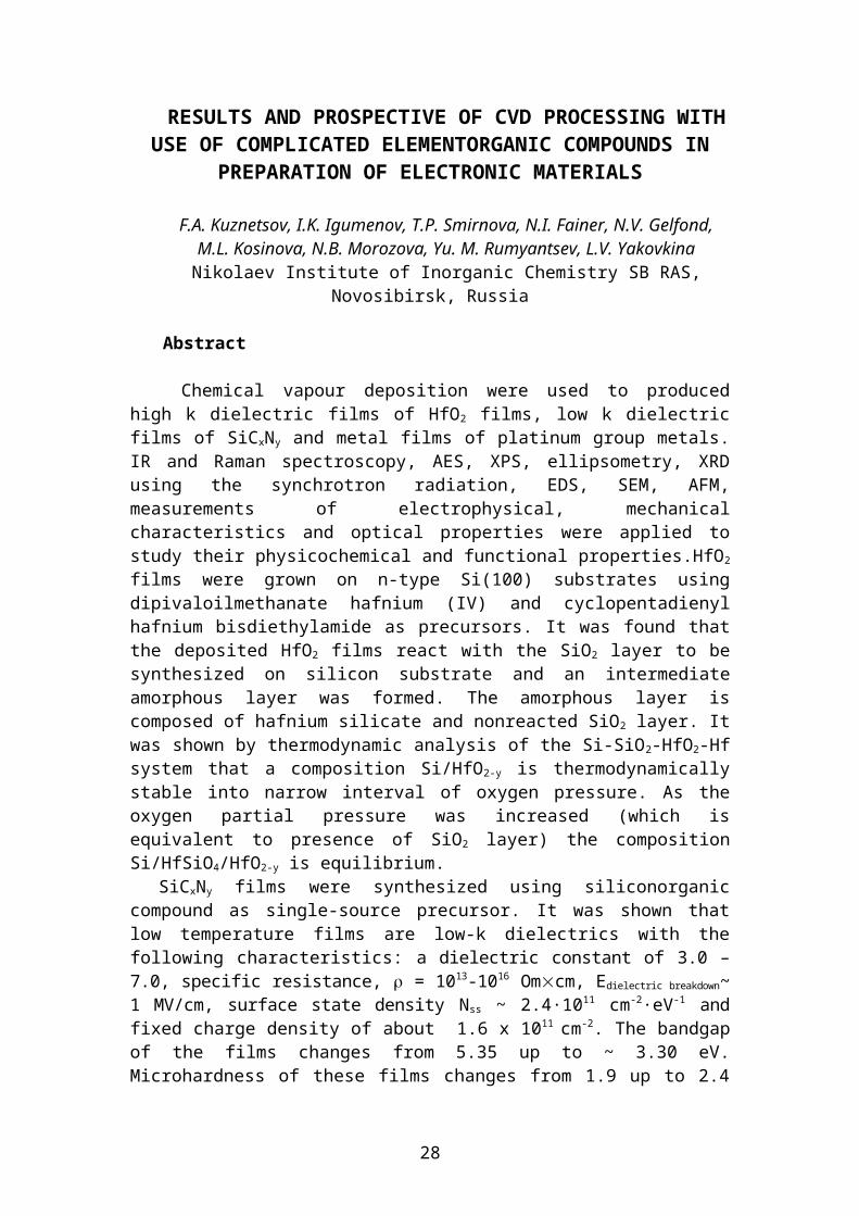
Fig 8. IR spectra of SiCxNy films obtained at 373 K and r. f. power of 15 W (a-b), 20 W (c), and 40 W (d). Total view (a) and deconvolution of the main 500-1350 cm-1 band (b-d) into components.
In contrast to high temperature films [45] there are hydrogenous bonds such as defor-mation stretching vibration of Si-CH3 bonds at 1250 cm-1, stretching vibration C-N or Si-CH2-Si bonds at ~1400 cm-1, stretching vibration of Si-H or N=C=N bonds at 2100-2200 cm-1, asymmetric stretching vibration of C-H bonds at 2900 cm-1, vibration of N-H at 3390 cm-1 (Fig. 9a) [46]. The main wide IR peak was approximated by sum Gaussian curves and their integral intensities were calculated. This analysis showed that the main IR adsorption band mostly corresponds to the superposition of asymmet-ric stretching vibration of N - Si - N bonds at 450 cm-1, symmetric stretching vibration of Si-N bonds at 950 cm-1, stretching vibration of Si-C bonds at 800 cm-1, and stretch-ing vibration of Si-O or C-N bond at 1030 cm-1. The increase of r.f. plasma power up to 40 W leads to the decrease of intensities or the disappearance of the IR bands relat-ing to hydrogenous bonds. This influence into chemical composition is to a greater extent then an increase of growth temperature (Fig. 9 b-d). The using of (HMDS+N2) gaseous mixture at similar Tgrowth and r.f. power leads to the decrease of integral inten-sity of S-C bond and increase of integral intensity of Si-N bond in SiCxNy films.
Raman spectroscopy. It was observed that Raman spectra of silicon carbonitride films grown at low temperatures and any r.f power represent continuous spectrum, separate peaks are absent. Lack of specific Raman spectrum with two broad bands centred at 1360 cm-1 and 1540 cm-1 (D- and G-bands) is probably explained that nano-crystals of disordered sp2 carbon do not form in silicon carbonitride films at these con-ditions.
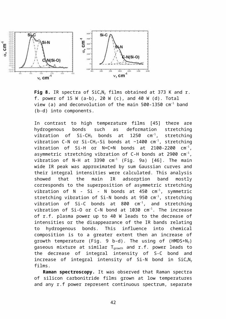
AES and XPS study. XPS spectra of C 1s, N 1s and Si 2p lines for a typical sample grown at temperature of 423 K, using (HMDS+N2) gaseous mixture as well as standard samples (Si, Si3N4, SiC and SiO2), were recorded. The photoelectron lines in the XPS spectra (Fig. 10) represent superposition of two or more components. All photoelectron lines were deconvoluted into minima spectral components based on the analysis of standard sample spectra and literature data.
37

Fig 9. X-ray photoelectron spectra of SiCxNy film grown at 423 K using (HMDS+N2) gaseous mixture.
A broad Si 2p peak consists of three subpeaks with energies of 100.5, 101.8 and 102.8 eV corresponding to Si-C, Si-N and Si-O bonding, respectively. This conclu-sion is supported by the values of modified Auger parameters of silicon measured as a difference between Si2p core level and Si KL23L23 Auger signal, excited by using the bremsstrahlung X-rays from the Al anode. The modified Auger parameter is also very sensitive to the chemical bonds of silicon with neighbouring atoms and what is more important, it does not depend on electrostatic charging of the sample. The Si Auger parameter, measured using standard samples, was equal to 1716.1 eV (elemental Si), 1715.4 eV (SiC), 1714.0 eV (Si3N4) and 1712.2 eV (SiO2) and coincided with literary data [47]. In case of synthesised SiCxNy films the Si Auger parameter for three com-ponents of Si 2p peak with energies of 100.5 (Si-C), 101.8 (Si-N) and 102.8 eV (Si-O) was equal to 1715.6, 1713.2 and 1712.4 eV, respectively.
Binding energies of two distinct components of N1s core level were found near 397.9 eV corresponding to N-Si bonding and ~ 400.2 eV corresponding to N-C (sp2) bonding. The C 1s spectra could be deconvoluted into four subpeaks with binding en-ergies of 280.6, 284.6, 285.3 and 288.5 eV corresponding to Si-C, C-C, C(sp2)-N and C-O bonding, respectively. There are some differences in the composition and the bonding types of SiCxNy films grown at 373-623 K and at 673-1023 K [48]. The XPS Si 2p spectra of high temperature films were deconvoluted into three subpeaks with binding energies of ~ 102.8, 101.7 and 101.0 eV corresponding to Si-O, Si-N and in-termediate position between Si-N and Si-C bonding, respectively, in contrast the ap-proximation of XPS Si 2p spectra of low temperature films consists of three subpeaks with binding energies of 100.5, 101.8 and 102.8 eV corresponding to Si-C, Si-N and Si-O bonding. These differences are probably caused by the presence of hydrogenous bonds in consequence of an incomplete decomposition of HMDS molecules during the low temperature and low r. f. power growth process.
EDS study. Elemental composition (Si, C, N, O) of low temperature SiCxNy
films was determined by EDS. Unfortunately, hydrogen concentration was noе mea-sured by both this method and other spectroscopic ones (Auger, XPS) though there were a lot of hydrogen bonds in FTIR spectra (Fig. 9a). The concentration of oxygen impurity is below 4 at. %. EDS data analysis showed, that to obtain dielectric films with low value of permittivity optimization of silicon, carbon and nitrogen concentra-tions is required (Table 1).
38

Table 1. Electrophysical parameters of SiCxNy films as function of element composi-tion
Electrophysical characteristics Elemental composition, at %
( сm) Ebr(V/сm) Si C N O3.0 3.2 1014 6.6 105 10.7 63.80 22.30 3.103.3 3.7 1014 7.5 105 7.12 61.40 19.03 3.493.3 1.7 1012 3.4 105 7.10 61.14 28.26 3.523.8 1.6 1014 2.5 105 7.06 60.67 28.77 3.514.3 3.5 1013 4.0 105 7.33 59.98 29.20 3.494.4 5.5 1015 4.8 105 26.92 44.4 25.38 3.305.1 2.0 1013 3.4 105 12.97 46.70 36.81 3.526.9 1,2 1015 8.1 105 19.00 20.66 56.97 3.37
XRD-SR study. The structure and phase composition of SiCxNy films were in-
vestigated by XRD-SR technique specially developed by us for thin films containing of lightweight elements [43-45, 48].
Fig. 10. XRD-SR pattern of SiCxNy film grown using (HMDS +He) mixture at 373 K. l=1.5405 Å.
The diffraction pattern of SiCxNy sample shown in Fig. 11 is typical one for all silicon carbonitrides films grown in all intervals of growth conditions This XRD-SR pattern shows that the peaks’ position is close to standard -Si3N4 phase. Lower in-tensity of XRD-SR peaks can be explained by lower concentration of nanocrystals in films grown at 373 K as compared with high temperature films [48]. We can imply that carbon atoms substitute only for the silicon sites without changes in valence in the α-Si3N4 structure so that C and Si are “bridged” by nitrogen in the SiCxNy films.
Microstructural features. Investigation of the micromorphology of the surface of these films by SEM and AFM showed that the films synthesized at low tempera-tures exhibit the flat smoothfaced surface with a root mean square roughness Rms of 0.5-1.0 nm.
Microhardness measurements. CSZM Nano Hardness tester was used to deter-mine the mechanical properties of SiCxNy films of 1 m thick. The measurements showed that the microhardness of low temperature silicon carbonitride films changes from 1.9 up to 2.4 GPa, and Young's modulus changes from 12.2 up to 15.9 GPa. These values are higher than ones for modern low-k and ultralow-k materials such as SiLK, MSQ, SiOCH, CF polymers, and so on. These materials, in general, have poor
39

mechanical characteristics as compared to SiO2 [49]. The obtained mechanical param-eters of low temperature films are considerably lower than that for high temperature SiCxNy films (H = 18 - 28 GPa, E = 135 - 185 GPa) synthesized by us early [48].
The C–V and I–V measurements. The electrical properties of SiCxNy films were retrieved from current-voltage (I-V) and high-frequency capacitance-voltage (C-V) measurements on MIS structures. Electrical measurements were performed at an au-tomated set-up based on two capacitive bridges. Measurement frequency was 1 MHz, amplitude of the testing signal was 20 mV. The MIS capacitors (S = 0.49 mm2) were manufactured by deposition of aluminum electrodes on the film surface by PVD through a mask. In order to determine the permittivity of SiCxNy film, we have mea-sured the voltage-capacity characteristics of MIS structures in which the films under investigation served as dielectrics, while n-type silicon substrates served as a semi-conductor. The permittivity k was calculated from the value of capacity of MIS struc-ture measured in the accumulation mode (positive potential on the metal).
An example of typical (C-V) and (I-V) of MIS structures with insulator film SiCxNy are presented in 12. 4. It should be noticed that the C-V and I-V curves shows classical behavior: distinct plateau in the accumulation region (C-V), variation of I (V) and clear breakdown voltage.
The fixed charge density of about 1.6 x 1011 cm-2 and the surface state density Nss
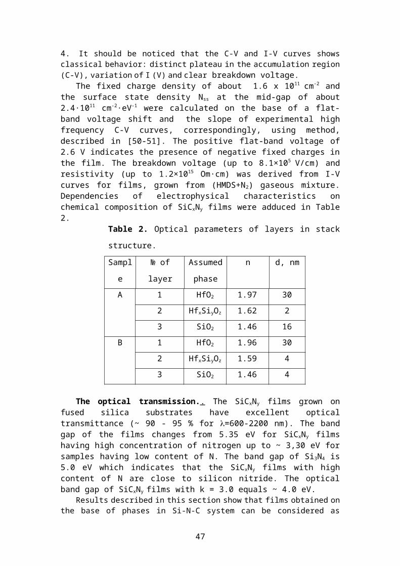
at the mid-gap of about 2.4·1011 cm-2·eV-1 were calculated on the base of a flat-band voltage shift and the slope of experimental high frequency C-V curves, correspond-ingly, using method, described in [50-51]. The positive flat-band voltage of 2.6 V in-dicates the presence of negative fixed charges in the film. The breakdown voltage (up to 8.1×10⁵ V/cm) and resistivity (up to 1.2×10¹⁵ Om·cm) was derived from I-V curves for films, grown from (HMDS+N2) gaseous mixture. Dependencies of electrophysical characteristics on chemical composition of SiCxNy films were adduced in Table 2.
Table 2. Optical parameters of layers in stack structure.
Sample № of layer Assumed
phase
n d, nm
A 1 HfO2 1.97 30
2 HfxSiyOz 1.62 2
3 SiO2 1.46 16
B 1 HfO2 1.96 30
2 HfxSiyOz 1.59 4
3 SiO2 1.46 4
The optical transmission.. The SiCxNy films grown on fused silica substrates have excellent optical transmittance (~ 90 - 95 % for l=600-2200 nm). The band gap of the films changes from 5.35 eV for SiCxNy films having high concentration of nitrogen up to ~ 3,30 eV for samples having low content of N. The band gap of Si3N4 is 5.0 eV which indicates that the SiCxNy films with high content of N are close to silicon ni-tride. The optical band gap of SiCxNy films with k = 3.0 equals ~ 4.0 eV.
Results described in this section show that films obtained on the base of phases in Si-N-C system can be considered as prospective dielectrics in solid state electronics. As it can be seen from reported results, this particular application does not limit possible use of the materials. A wide range of transmittance, high value of hardness, chemical stability of
40

the materials make them prospective for use in other areas of technology: optics, mi-cromechanics, technology of high pure materials and so on.
Metal Films
CVD processing can be used for deposition of a big number of metals and metal alloys. In this paper we give results of investigation of deposition of metal of platinum group, which can be used for interconnections in highly integrated electronic schemes. Acetyl acatonates of different platinum group metals were used as precursors.
Experimental ProceduresDepositions. Three MOCVD reactors were used to deposit platinum group met-
als [52-56]. The gas streams rates (argon, hydrogen and oxygen) were controlled and monitored using mass flow meters (range: 1 to 24L/h). Both evaporator and substrate temperature were thermostatically controlled. The evaporator temperature ranged 443 K for Ir(acac)3, and from 433 to 453 K for Pt(acac)2. The deposition temperature ranged from 643 to 823 K for Ir(acac)3, and from 623 to 723 K for Pt(acac)2. The total pressure was monitored and controlled independently of the gas flow: atmospheric pressure for Ir(acac)3, 4 Torr for Pt(acac)2. Palladium and rhodium thick coatings were deposited on Mo substrate at temperatures of 543 to 573 and 723 to 773 K respec-tively, at total pressures of 1 to 10 and 1 to 330 Torr, respectively. The evaporator temperature ranged from 313 to 393 K for Pd(hfac)2 and from 443 to 493 K for Rh(acac)3. The deposition of Pt, Ir, Rh coatings was carried out both in the presence of hydrogen and oxygen. Good knowledge of thermal behaviour of these precursors was at hand [57-63]. Depositions were carried out mainly on glass, quartz glass and stainless steel.
Analysis of samples. Some platinum coatings obtained on glass were thick and had low adhesion. These films were carefully removed in water, dried and glued with epoxy glue between slices of silicon. The obtained multi-layer compound was then enclosed in a brass tube and sewed perpendicularly to the coating plane into 70µm thick slides. These slices were then ground with dimple grinder and ion milled. These cross-section samples were observed with a High Resolution Transmission Electron Microscope FEI “TECHNAI G²” (200kV), with a Schottky Field Emission Source (FEG), which allows 0.5 nm probes. For qualitative element analysis, Energy Disper-sive X-Ray (EDX), and GatanTM Image Filter (GIF) techniques were used. The irid-ium coatings obtained on quartz glass were separated by dissolution of quartz glass substrate into fluor-hydric acid. The films were then placed on a grid and observed with Transmission Electron Microscope JEM-100 CX. This procedure is described in [64]. In the case of Pd and Rh coatings, the phase composition of the coatings was studied by means of X-ray phase analysis in the angle range 2 from 5 to 80o. The ele-ment composition was analysed by layer-by-layer sputtering of the sample surface by laser radiation directly in the ion source of the mass spectrometer. Structure of coating was observed by scanning electron microscopy.
ResultsDeposition of Pt, Ir, Rh and Pd. The results obtained from numerous experi-
ments allowed to draw some general experimental guidelines for the deposition of Pt group metal coatings:
Reactor conception: It must allow to separate the flows of complex vapour and reactant gas spatially [53, 61, 65].
41
Precursor choice: Due to the high catalytic activity of platinum metals and the high cost of Pt group metal-based compounds, the chosen precursors must be able to achieve a transformation degree of at least 60 to 80% for the whole sequence of con-versions: metal - initial salt - precursor - purification - gas phase transport to the sub-strate - thermal decomposition - coating. It has been shown earlier, on the basis of the analysis of literature data and our experiments, that at present -diketonates of plat-inum metals best meet this whole set of requirements.
Phase composition of thick coatings: We have found mainly crystal phases of the corresponding metals. Rhodium deposition in the presence of oxygen leads to the ad-ditional lines corresponding to rhodium oxides in the diffraction patterns [53].
Total content of aerogenic impurities in the coatings does not exceed 210-2
mass.%. Carbon content decreases in 2 times with using oxygen as a gas reactant in comparison with coating deposition in the presence of hydrogen [53].
Surface morphology of thick coating: Scanning electron microscopy investiga-tions showed that the size of characteristic surface elements is decreased with decreas-ing precursor concentration in deposition zone [53].
Thick coatings are characterized by the decrease of surface element size from the outer surface of the sample to the metal-substrate boundary as it was observed for Pd coatings (50-200 m thick) [53].
Deposition conditions as well as substrate material have also a strong influence on coating microstructure and composition [52-56, 64, 66, 67].
In order to understand the mechanism of coating growth and the effects of depo-sition temperature, the initial growth stages of depositions were observed in the case of iridium.
Study of initial stages of coating growth (Ir) The first stages of the depositions were carried out on quartz glass at atmospheric pressure under hydrogen atmosphere [64].
Fig. 11 a, b, c. Initial structures of Ir films obtained with deposition temperature of 643, 693 and 803 K: a) 643 K: microcrystallites (50-100 Å) aggregated in secondary islands (500-1000 Å)b) 693 K: microcrystallites (200-500 Å) aggregated in secondary islands (up to sev-eral thousands Å)
42
As can be seen in Fig. 13, the initial structures at lower temperatures (under 773 K) are iridium micro-crystallites (50-200 Å depending on deposition temperature) ag-gregated in secondary islands (in order of 1000 Å). Above 773 K another initial struc-ture is observed, namely ordered dendrites with cross sizes of 500 Å and more. The crystals of Ir films were (111) oriented [64].
The observed crystallization of Ir films can not be described as a process of nu-cleation and gradual micro-crystallite sintering, which is typical process for ideally pure materials. Features in growth of iridium films at different deposition tempera-tures could be explained by the presence of insignificant amount of carbon-containing by-products coming from thermal decomposition of iridium precursor.
Fig. 12. Thin amorphous layers on surface of Ir crystallites in initial structures of Ir films obtained with deposition temperature of 743 K. Substrate - quartz glass
We have detected thin amorphous layers with thickness of 10-20 Å (Fig. 14) on surface of Ir crystallites in films deposited at temperature of 743 and above. Such lay-ers not form at lower temperatures. It is known that carbon solubility in iridium is in-significant in a wide temperature range (up to 2100 K) [68]. That’s why we believe that at lower temperatures carbon-containing by-products segregate on inter block boundaries and prevent from iridium crystallization in large particles.
At increasing deposition temperatures, iridium crystallization occurs and carbon-containing by-products diffuse on island surfaces with the formation of thin surface layers. This process could lead to change mechanism of coating growth during deposi-tion process, as was observed with Pt (see next sections).
Ir coatings shown here are obtained under hydrogen atmosphere. Investigation on thermal decomposition of Ir(acac)3 vapor on hot substrate [60, 63] proved that D2 and therefore H2 shift the reaction in direction of formation of free ligand instead of prod-ucts of deep destruction of the compound. This results in reduction of pollution of Ir films by carbon. According source [69], use of oxygen also leads to carbon free Pt and Ir films.
At high growth rate we observed coatings with columnar structures for all plat-inum group metals in hydrogen and in oxygen atmospheres. It was decided to study more in details the mechanisms of formation of this structure.
Columnar microstructures in thick coatings (Ir, Pd, Pt) Effect of deposition temperature on internal microstructure of coatings was observed in our studies of thick Ir depositions in oxygen and hydrogen atmospheres [55]. It was shown that de-creasing deposition temperature leads to obtaining more compact structure.
Raising Ir deposition temperature causes some increase of oxygen content in the coating, most likely, due to encapsulation in faster growing iridium coating. The de-
43

crease of the deposition temperature of iridium coatings in the presence of oxygen leads to obtaining a more perfect structure and also to the decrease of the dimensions of the regions of coherent scattering (crystallites, slits, etc.). With higher deposition rates columnar structure is obtained (Fig. 15a).
Fig. 13. Columnar structures. (a) Thick Ir deposition in oxygen at atmospheric pres-sure, substrate temp.: 593 K. (b) Thick Pd deposition in hydrogen at 3 Torr, substrate temp.: 553 K.
This was also observed in the case of Pd, where the decrease of the deposition temper-ature leads to obtaining a more perfect structure while higher deposition temperature is associated with a change in structure toward columnar structure (Fig. 15b).
The suggestion that the adsorption of precursor decomposition products in the coating plays a role in this change of microstructure was investigated into more details in the case of Pt depositions.
In the case of Pt, columnar structures were also observed. In certain deposition conditions, the coating showed two very different micro-structural zones, arranged in the coating growth direction. At a critical thickness, the deposition ceases to produce a compact coating, and instead, an irregular structure appears, with a basaltic/columnar aspect (Fig. 16).
Fig. 14. Transversal section of Pt-coatings showing the transition from a compact to a columnar structure at a thickness of 100 to 200 nm. Deposition at 653 K (left) and 723 K (Right) show similar morphologies. Substrate: glass
This behavior is observed on glass and stainless steel substrates at the same critical thickness. In the investigated range, the deposition temperature affects neither of these phenomena.
44

Fig. 15. XRD Analysis of the compact (a) and columnar zone (b) of a Pt coating. Compact zone displays a strong (111) orientation while columnar zone shows a (200) orientation
XRD studies (Fig. 17) show that the crystallography of the inferior zone corre-sponds to a (111) texture. The columnar zone shows a (200) orientation. The (200) structure is not compact, and the (200) columnar morphology remains stable during further growth.
Fig. 16. TEM Cross-section of Pt coating, (a): Compact, equiaxed zone; (b): Colum-nar zone; (c): “White zone”; (d): Transition / Competition zone.
High Resolution Transmission Electron Microscopy investigations showed four different layers (Fig. 18). (a): A compact layer of a homogeneous thickness presenting a perfect (111) stacking. It exhibits a very small grain size (50-100nm). (b): The basaltic / columnar structures, already observed by SEM. (c): An extremely thin layer (a few nm) which was called “White zones”. This seems to be the starting point of the structural change. (d): A transition zone containing mostly (111) grains and some (200) grains. These grains had an average diameter of about 50 nm. In this region there seems to be a growth competition between the (111) and (200) grains. The (200) grains are the origin of the basaltic structures that are emerging.
45

The aspect of white zones looked massively disturbed. The presence of hetero-atoms could be responsible for such crystal distortions: For various reasons, the choice was limited to carbon and oxygen coming from the precursor. The distribution of oxygen was observed with EDX and appeared somewhat equally distributed along the coating depth. In contrast, the GIF observation reveal that white zones are rich in carbon. It can be affirmed that carbon content is above solubility limit (2,5 atomic percent) [52, 54].
Observations suggest that precursor molecules let a residual amount of carbon content in the deposited coatings. This residual carbon concentrates itself in a superfi-cial layer on top of the metallic compact layer since the early stages of deposition.
As it was observed in the case of Ir, amorphous carbon is observed at the surface of the Ir crystallites from the very first step of deposition process. In the case of Pt, a carbon rich phase (“white zones”) precipitates after a given deposition thickness.
We suggest that by-products of precursors decomposition (Ir(acac)3 and Pt(acac)2
respectively) could increase carbon content into the superficial layer, until precipita-tion occurs at the solubility limit.
In the specific case of platinum, the growth of (200) grains can be explained con-sidering the very short mean free path of gas molecules (typically less than 1 Angstrom) and the stacking due to the high concentration of precursor molecules. Molecules of precursor have no freedom to move to the energetically favorable sites and a constant deposition rate is achieved on every grain. Due to their lower atomic density along the growth direction, (200) grains grow faster than (111) grains with the same atomic deposition rate and win the competition. As a result, lower precursor par-tial pressure in the CVD atmosphere is also a suggested way to increases the quality of coating.
Discussion Some applications require compact and clean coatings (high temperature oxida-
tion protective coatings for example). On the other hand, coatings with columnar structure with high specific surface area can be extremely appealing for different cata-lytic and electrochemical applications.
Several factors were found to influence coating quality. First, in the case of thick Ir coatings, more compact structures were obtained when deposition was carried out in oxygen atmosphere than in hydrogen atmosphere. We attribute these results to the decarburizing effect of oxygen atmosphere, which leads to lower carbon content in the film. The effect of decarburizing species like oxygen and water vapor were also con-firmed in literature [70].
It was also observed that decreasing deposition temperature leads to lower crystal size and obtaining more compact structures. A possible explanation could be the smaller particle size on initial stages, as observed in Ir depositions at lower deposition temperatures. Other studies in literature confirmed our observations that decreasing deposition temperature results in obtaining Pt coatings with a more compact (111) structure [70].
A third observation was the effect of precursor concentration. With decreasing precursor concentration in deposition zone, the size of surface elements is also de-creased. We propose an explanation based on mobility of precursor molecule. With decreasing concentration, the molecules mobility increases. Particles have possibility to reach the more energy-favorable sites of deposition, and the evacuation of decom-position by-products is made easier.
46
General conclusionCVD processing has played very essential role in development of present day
solid state electronics. However till now a very limited selection of volatile com-pounds –CVD precursors were used. Actually the selection id limited to halogenides and hydrides. Only very simple metal organic compounds were recently introduced in electronic devices technology. Introduction of multiple volatile compounds known now to chemists is restricted by insufficient knowledge of mechanisms of the pro-cesses with these compounds, requirements to have the compounds in state of high purity. So, one of the purposes of our study was to show that a big potential for fur-ther development of electronic materials processing is in use of complicated metal or-ganic compounds. Specific task was to solve some problem related to continuation of miniaturization of silicon electronics which can not be done without introduction of new materials to replace traditional constituent of electronic devices.
We are convinced that a wide use of MO CDV will also be useful for “post sili-con” electronics which has to come in predictable future.
References1. P.A. Packan, Science 285 (1999) 2079.2. D.A. Buchanan and S.-H. Lo, Microelectron. Eng. 36 (1997) 13.3. J. Robertson, Eur. Phys. J. Appl. Phys. 28 (2004) 265.4. J.-H. Lee, Thin Solid Films 472 (2005) 317. 5. Naek S. Yang, Ki-Seok An, Eun-Joo Lee, Wontae Cho, Hong S. Jung, Sun K. Park, Yang K. Lee, Taek-Mo Chung, Chang G. Kim, Sungmoon Kim, Jin-Ha Hwang, Choongkeun Lee, Nam-Soo Lee, Yunsoo Kim, Chem. Mat. 17 (2005) 6713.6. H. Kato, T. Nango, T. Miyagawa, T. Katagiri, K.S. Seol, Y. Ohki, J. Appl. Phys. 92 (2002) 1106.7. N. Miyata, T. Nabatame, T. Horikawa, M. Ichikawa, A. Toriumi, Appl. Phys. Lett. 82 (2003) 3880.8. H. Wong, B. Sen, V. Filip, M.C. Poon, Thin Solid Films 504 (2006) 192. 9. S.J. Wang, P.S. Lim, A.C.H. Huan, C.L. Liu, J.W Chai, S.Y. Chow, J.S. Pan, Q. Li., C.K. Ong, Appl. Phys. Let. 82 (2003) 2047. 10. H. Kim, P.S. Mclnture, J. Appl. Phys. 92 (2002) 5094. 11. R. Xu, Z.J. Yan, S. Chen, Y.L. Fan, X.M. Ding, Z.M. Jiang, Z.S. Li, Surf. Sci. 581 (2005) 236. 12. Kaupo Kukli, Tero Pilvi, Mikko Ritala, Timo Sajavaara, Jun Lu, Markku Leskela, Thin Solid Films 491 (2005) 328.13. Andrew R. Teren, Reji Thomas, Jiaqing He, Peter Ehrhart, Thin Solid Films, 478 (2005) 206.14. Y. Ohshita, A. Ogura, A. Hoshino, S. Hiiro, T. Suzuki, H. Machida, Thin Solid Films 46 (2002) 21515. L.V. Yakovkina, V.N. Kitchai, T.P. Smirnova, V.V. Kaichev, Yu.N. Shubin, N.B. Morozova, K.V. Zherikova, I.K. Igumenov, Inorganic Materials 41 (2005) 130.16. ICDD/JCPDS database of crystallographic data: http://www.icdd.com / 17. J. Aarik, A. Aidla, A.-A. Kiisler, T. Uustare, V. Sammelselg, Thin Solid Films 340 (1999) 110. 18. L.A. Giannuzzi, F.A. Stevie, Micron 30 (1999) 197.19. S. Rubanov, P.R. Munroe, Mater. Lett. 57 (2003) 2238.20. Handbook of X-ray photoelectron spectroscopy, edited by C.D. Wagner, W.M. Riggs, L.E. Davis, J.F. Moulder, G.E. Muilenberg, Perkin-Elmer, Minnesota. 1978.
47

21. S.V. Pasko, L.G. Hubert-Pfalzgraf, A. Abrutis, P. Richard, A. Bartasyte, V. Kazlauskiene, J. Mater. Chem. 14 (2004) 1245.22. S.V. Pasko, A. Abrutis, L.G. Hubert-Pfalzgraf, Mater. Lett. 59 (2005) 261.23. M.-H. Cho, Y. S. Roh, C.N. Whang, K. Jeong, S.W. Nahm, D.H. Ko, J.H. Lee, N.I. Lee, K. Fujihara, Appl. Phys. Lett. 81 (2002) 472.24. Q. Fang, J.-Y. Zhang, Z. Wang, M. Modreanu, B.J. O’Sullivan, P.K. Hurley, T.L. Leedham, D. Hywel, M. A. Audier, C. Jimenez, J.-P. Senteur, I.W. Boyd, Thin Solid Films 453-454 (2004) 203.25. H. Borchert, Y.V. Frolova, V.V. Kaichev, I.P. Prosvirin, G.M. Alikina, A.I. Lukashevich, V.I. Zaikovskii, E.M. Moroz, S.N. Trukhan, V.P. Ivanov, E.A. Paukshtis, V.I. Bukhtiyarov, V.A. Sadykov, J. Phys. Chem. B 109 (2005) 5728.26. S. Suzer, S. Sayan, M.M. Banaszak Holl, E. Garfunkel, Z. Hussain, N. M. Hamdan, J. Vac. Sci. Technol. A 21 (2003) 106.27 W. Nieveen, B.W. Schueler, G. Goodman, P. Schnabel, J. Moskito, I. Mowat, G. Chao, Appl. Surf. Sci. 231-232 (2004) 556.28. G.D. Wilk, R.M. Wallace, J.M. Anthony, J. Appl. Phys. 87 (2000) 484.29. R. Thielsch, A. Gatto, J. Heber, N. Kaiser, Thin Solid Films, 410 (2002) 86. 30. A.E. Vol, Structure and Properties of Double Metallic Systems. Vol. II. Moscow Science, 1962 (in Russian).31. E. Rudy, P. Stecher, J. Less-Common Metals 5 (1963) 78.32 R. F. Domagala, R. Ruh, Amer. Soc. Metals Trans. Quart. 58 (1965) 164. 33. N.A. Toropov, V.P. Barzakovski, I.A. Bondar, Yu.P. Udalov, Equilibrium Dia-grams of Silicate System. Leningrad Science. 1969 (in Russian).34. D.L. Ageeva, Equilibrium diagrams of nonmetallic systems, «Totals of science». 1966. (in Russian).35. R. Beyers, J. Appl. Phys. 56 (1984) 147.36. K.J. Hubbard, D.C. Schlom, J. Mater. Res. 11 (1996) 2757.37. M. Gutowski, J.E. Jaffe, C.-L. Liu, M. Stoker, R.I. Hegde, R.S. Rai, P.J. Tobin, Appl. Phys. Lett. 80 (2002) 1897.38. A. Navrotsky, J. Mater. Chem. 15 (2005) 1883.39. S. Boughaba, G.I. Sproule, J.P. McCaffrey et al, Thin Solid Films, 402 (2002) 99.40. I.V. Afanasyev-Charkin, M. Nastasi, NIM B, 206 (2003) 736.41. A. Bendeddouche, J.Appl.Phys. 81 (1997) 6147.42. A. Badzian, J. Am. Ceram. Soc., 85 (2002) 16.43. N.I. Fainer, M.L. Kosinova, Yu.M. Rumyantsev, F.A. Kuznetsov, J. Phys. IV, 9 (1999) 769.44. N.I. Fainer, Yu.M. Rumyantsev, A.N. Golubenko, M.L. Kosinova, F.A. Kuznetsov, J. Crys. Growth, 248C (2003) 175.45. N.I. Fainer, M.L. Kosinova, Yu.M. Rumyantsev et al, Glass Physics and Chem-istry, 31 (2005) 427.46. E. Vassallo, A. Cremona, F. Ghezzi et al, App. Sur. Sci., 252 (2006) 7993. 47. C.D. Wagner, L.E. Davis, M.V. Zeller, et al, Surf. Interface Anal. 3 (1981) 211.48. N.I. Fainer, M.L. Kosinova, Yu.M. Rumyantsev, et al, ECS Proc. Fifteenth Euro-pean Conference on Chemical Vapor Deposition, 2005-09 (2005) 1074.49. K. Maex, M.R. Baklanov, D. Shamiryan, et al, J. Appl. Phys., 93 (2003) 8794.50. L.M. Terman , Solid State Electronics, 5 (1962) 28551. E.H. Nicollian, J.R. Brews, MOS Physics and Technology, (Willey, New York, 1982).52. H. Nizard, N.V. Gelfond, N.B. Morozova, I.K. Igumenov, L. Gimeno-Fabra, A. Redjaimia, Electrochemical society proceedings 9 (2005), 754.
48

53. I.K. Igumenov, N.V. Gelfond, R.H. Tuffias, Electrochemical Society Proceedings 25 (1997), 1618.54. L. Gimeno-Fabra, H. Nizard, H. Benien, J. Vlcek, A. Redjaimia, Materials Sci-ence and Engineering Technology 34 (2003), 410.55. I.K. Igumenov, N.V. Gelfond, N.B. Morozova, P.P. Semyannikov, S.V. Trubin, V.S. Danilovich, L. Gimeno-Fabra, 8 (2003), 1327.56. N.V. Gelfond, F.V. Tuzikov, I.K. Igumenov, Thin Solid Films 227 (1993), 144.57. G.I. Zharkova, I.K. Igumenov, S.V. Tkachev, S.V. Zemskov, Koord. Khim. 8 (1982), 74 (in Russian).58. G.I. Zharkova, I.K. Igumenov, S.V. Zemskov, Koord. Khim. 9 (1983), 845 (in Russian).59. V.G. Isakova, I.K. Igumenov, S.V. Zemskov, Koord. Khim. 11 (1985), 1377 (in Russian).60. V.G. Isakova, P.P. Semyannikov, V.M. Grankin, I.K. Igumenov, Koord. Khim. 14 (1988), 57 (in Russian).61. I.K. Igumenov, J. de Physique IV C5 (1995), 489.62. N.B. Morozova, G.I. Zharkova, P.P. Semyannikov, S.V. Sysoev, I.K. Igumenov, N.E. Fedotova, N.V. Gelfond, J. de Physique IV 11 (2001), 609.63. I.K. Igumenov, A.E. Turgambaeva, P.P. Semyannikov, J. de Physique IV 11 (2001), 505.64. N.V. Gelfond, V.I. Zaikovskii, I.K. Igumenov, Poverkhnost’ 5 (1994), 50 (in Rus-sian).65. F. Maury, J. de Physique IV C5 (1995), 449.66. N.V. Gelfond, I.K. Igumenov, A.I. Boronin, V.I. Bukhtiyarov, M.Yu. Smirnov, I.P. Prosvirin, R.I. Kwon, Surface Science 275 (1992), 323.67. N.V. Gelfond, A.I. Boronin, M.Yu. Smirnov, R.I. Kvon, I.K. Igumenov, Electro-chemical Society Proceedings 25 (1997), 1588.68. A.Ya. Tontegone, Poverkhnost’ 8 (1988), 13 (in Russian)69. T. Goto, R.J. Vargas, T. Hirai, Mater. Trans. 40 (1999), 209.70. G.A. Battiston, R. Gerbasi, A. Rodrigues, Chem. Vap. Deposition 11 (2005), 130.
49