Resonant Field Enhancement of Epsilon Near Zero Berreman ...
10
Resonant Field Enhancement of Epsilon Near Zero Berreman Modes in an Ultrathin AlN Film Nikolai Christian Passler, *,† Ilya Razdolski, † D. Scott Katzer, ‡ David F. Storm, ‡ Joshua D. Caldwell, ‡,¶ Martin Wolf, † and Alexander Paarmann *,† †Fritz-Haber-Institut der Max-Planck-Gesellschaft, Faradayweg 4-6,14195 Berlin, Germany ‡US Naval Research Laboratory, 4555 Overlook Avenue SW, Washington DC 20375, USA ¶Vanderbilt Institute of Nanoscale Science and Engineering, 2201 West End Ave, PMB 350106, Nashville, TN 37235-0106, USA E-mail: [email protected]; [email protected] Abstract Enormous optical field enhancement was pre- dicted to occur for the Berreman mode in ul- trathin films in the vicinity of epsilon near zero (ENZ). Here, we report the first exper- imental proof of this prediction in the mid- infrared by probing the resonantly enhanced second harmonic generation (SHG) at the lon- gitudinal optic phonon frequency from a deeply subwavelength-thin aluminum nitride (AlN) film. Employing a transfer matrix formalism, we show that the field enhancement is com- pletely localized inside the AlN layer, revealing that the observed SHG signal of the Berreman mode is solely generated in the AlN film. Our results demonstrate that ENZ Berreman modes in intrinsically low-loss polar dielectric crystals constitute a promising platform for nonlinear nanophotonic applications. Keywords Berreman mode, epsilon near zero, infrared, nanophotonics, second harmonic generation, field enhancement In nanophotonics, nonlinear optical phenom- ena are driven by the enhancement of local optical fields, which arises due to polaritonic resonances. These are traditionally observed as plasmon polaritons in metallic nanostruc- tures or rough metal surfaces. Such strongly enhanced fields enable a variety of nanoscale applications 1 such as all-optical switching, 2,3 low-loss frequency conversion, 4,5 and highly ef- ficient sensing. 6,7 In the infrared (IR), an al- ternative to plasmonic resonances in metals are phonon polaritons supported in polar crystals, 8 as has been demonstrated in various seminal studies. 9–12 These phonon polaritons feature longer lifetimes than plasmon polaritons, lead- ing to much larger quality factors and stronger field enhancements, 13–15 and thus potentially enhanced efficiency of nonlinear optical effects. One area in nanophotonics of distinct recent interest are investigations of polaritonic modes in plasmonic or polar dielectric subwavelength- thin films that emerge near zero permittivity. Over the past decades, the existence of such thin-film polaritonic modes has attracted broad attention. 16–24 Initially, radiation in a narrow spectral window at the plasma frequency of thin metal films was predicted 16 and later ob- served. 18–20 Its origin was associated with a col- lective surface plasma mode with polarization normal to the surface plane of the film. 18 At the same time, a similar effect was reported by Berreman in a thin polar dielectric film, 17 where absorption occurs at the longitudinal op- tic (LO) phonon frequency. These absorption features in thin films were 1 arXiv:1811.10370v1 [physics.optics] 26 Nov 2018
Transcript of Resonant Field Enhancement of Epsilon Near Zero Berreman ...

Resonant Field Enhancement of Epsilon NearZero Berreman Modes in an Ultrathin AlN Film
Nikolai Christian Passler,∗,† Ilya Razdolski,† D. Scott Katzer,‡ David F. Storm,‡
Joshua D. Caldwell,‡,¶ Martin Wolf,† and Alexander Paarmann∗,†
†Fritz-Haber-Institut der Max-Planck-Gesellschaft, Faradayweg 4-6,14195 Berlin, Germany‡US Naval Research Laboratory, 4555 Overlook Avenue SW, Washington DC 20375, USA¶Vanderbilt Institute of Nanoscale Science and Engineering, 2201 West End Ave, PMB
350106, Nashville, TN 37235-0106, USA
E-mail: [email protected]; [email protected]
Abstract
Enormous optical field enhancement was pre-dicted to occur for the Berreman mode in ul-trathin films in the vicinity of epsilon nearzero (ENZ). Here, we report the first exper-imental proof of this prediction in the mid-infrared by probing the resonantly enhancedsecond harmonic generation (SHG) at the lon-gitudinal optic phonon frequency from a deeplysubwavelength-thin aluminum nitride (AlN)film. Employing a transfer matrix formalism,we show that the field enhancement is com-pletely localized inside the AlN layer, revealingthat the observed SHG signal of the Berremanmode is solely generated in the AlN film. Ourresults demonstrate that ENZ Berreman modesin intrinsically low-loss polar dielectric crystalsconstitute a promising platform for nonlinearnanophotonic applications.
Keywords
Berreman mode, epsilon near zero, infrared,nanophotonics, second harmonic generation,field enhancement
In nanophotonics, nonlinear optical phenom-ena are driven by the enhancement of localoptical fields, which arises due to polaritonicresonances. These are traditionally observed
as plasmon polaritons in metallic nanostruc-tures or rough metal surfaces. Such stronglyenhanced fields enable a variety of nanoscaleapplications1 such as all-optical switching,2,3
low-loss frequency conversion,4,5 and highly ef-ficient sensing.6,7 In the infrared (IR), an al-ternative to plasmonic resonances in metals arephonon polaritons supported in polar crystals,8
as has been demonstrated in various seminalstudies.9–12 These phonon polaritons featurelonger lifetimes than plasmon polaritons, lead-ing to much larger quality factors and strongerfield enhancements,13–15 and thus potentiallyenhanced efficiency of nonlinear optical effects.
One area in nanophotonics of distinct recentinterest are investigations of polaritonic modesin plasmonic or polar dielectric subwavelength-thin films that emerge near zero permittivity.Over the past decades, the existence of suchthin-film polaritonic modes has attracted broadattention.16–24 Initially, radiation in a narrowspectral window at the plasma frequency ofthin metal films was predicted16 and later ob-served.18–20 Its origin was associated with a col-lective surface plasma mode with polarizationnormal to the surface plane of the film.18 Atthe same time, a similar effect was reportedby Berreman in a thin polar dielectric film,17
where absorption occurs at the longitudinal op-tic (LO) phonon frequency.
These absorption features in thin films were
1
arX
iv:1
811.
1037
0v1
[ph
ysic
s.op
tics]
26
Nov
201
8
argued to originate in radiative virtual polari-tonic modes,21–23 naturally occurring at fre-quencies where the real part of the dielectricfunction crosses zero. This condition is met atthe plasma frequency in a metal, and at theLO frequency of a polar crystal film. Whilethese lossy polariton modes disperse on the lowmomentum side of the light line, it was dis-covered that a complementary evanescent po-lariton mode close to the LO frequency of apolar dielectric is also supported outside thelight cone.22 Just like the radiative modes, theevanescent polaritons naturally emerge in thinfilms at frequencies of vanishing dielectric func-tion. Therefore, these modes offer an intriguingplatform for exploiting the unique characteris-tics of waves propagating in so called epsilonnear zero (ENZ) materials.25,26
While most ENZ studies depend on carefullyand intricately designed metamaterials,27–29
thin metal or polar dielectric films stand outfor their structural simplicity. Previous studieshave reported promising applications employ-ing these ENZ polariton modes, such as opto-electronic devices for the ultrafast control of ab-sorption and emissivity,30–32 directionally per-fect absorption,33,34 or long-range plasmon po-laritons for the development of nanophotonicintegrated technologies.35,36
However, these previous studies mostly fo-cused on the linear optical response, whereasonly few reports of the nonlinear conversion ef-ficiency of ultrathin films exist. This efficiencyhas been proposed to be strongly enhanced atENZ frequencies,37 but experimental verifica-tion is limited to a few studies of indium tinoxide (ITO) thin layers38–40 excited at frequen-cies in the near infrared spectral range. Thenonlinear optical response of thin films of othermaterials with phonon resonances in the mid-to far-IR, in particular III-V or III-nitride polarsemiconductor compounds, however, has to thebest of our knowledge not yet been studied.
In this work, we investigate the linearand nonlinear optical response of ultrathin( λ/1000) AlN films on a SiC substrate inthe radiative regime, where λ represents thefree-space wavelength at the ENZ condition.We report strong SHG at the AlN LO phonon
frequency arising from the Berreman mode inthe ultrathin AlN film. The observed SHGyield provides experimental proof of the im-mense field enhancement inside the film and isattributed to the excitation of the Berremanresonance. Furthermore, we delineate severalperspectives based on ENZ polaritons for thedeployment of low-loss nonlinear nanophotonicapplications.
A mode in a medium is defined as a solution ofMaxwell’s equations in the absence of an exter-nal perturbation. In a three-layer system, thedispersion of a polaritonic mode can be calcu-lated by numerical evaluation of the followingformula:20,24,41
1 +ε1kz3ε3kz1
= i tan (kz2d)
(ε2kz3ε3kz2
+ε1kz2ε2kz1
),
(1)
where ε is the dielectric function, d is the film
thickness of layer 2, kzi =√
ω2
c2εi − k2x is the
out-of-plane momentum, kx is the in-plane mo-mentum conserved in all layers, and the sub-scripts i = 1, 2, 3 refer to the three layered me-dia. Note that all solutions shown here are cal-culated assuming a complex frequency ω andsolved for a real wavevector kx.
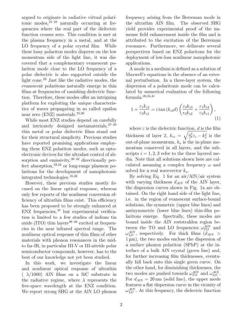
By solving Eq. 1 for an air/AlN/air systemwith varying thickness dAlN of the AlN layer,the dispersion curves shown in Fig. 1a are ob-tained. On the right hand side of the light line,i.e. in the region of evanescent surface-boundsolutions, the symmetric (upper blue lines) andantisymmetric (lower blue lines) thin-film po-laritons emerge. Spectrally, these modes arebound inside the AlN reststrahlen region be-tween the TO and LO frequencies ωAlN
TO andωAlNLO , respectively. For thick films (dAlN >
1 µm), the two modes enclose the dispersion ofa surface phonon polariton (SPhP) at the in-terface of a bulk AlN crystal (green line) and,for further increasing film thicknesses, eventu-ally fall back onto this single green curve. Onthe other hand, for diminishing thicknesses, thetwo modes are pushed towards ωAlN
TO and ωAlNLO .
For dAlN = 20 nm (solid line), the upper modefeatures a flat dispersion curve in the vicinity ofωAlNLO . At this frequency, the dielectric function
2

0.4 0.6 0.8 1.0Inplane momentum k (1/μm)
600
650
700
750
800
850
900
950
Wav
enu
mb
erω
(1/c
m)
leaky evanescent
ωLOAlN
ωTOAlN
Berreman modeThin film polaritonSPhP
b
a
203001000
dAlN in nm
600 700 800 900 10000.0
0.2
0.4
0.6
0.8
1.0
Refl
ecta
nce
0.2
0.4
0.6
0.8
1.0
Refl
ecta
nce
Wavenumber ω (1/cm)
ωTOAlN ωLO
AlN
c
203001000
dAlN in nm
enil thgil
symmetric
antisymmetric
Figure 1: Berreman mode in a freestand-ing AlN film and on a SiC substrate. aCalculated dispersions of the Berreman modeand thin film polaritons in a freestanding AlNfilm, and that of a SPhP at the surface of abulk AlN crystal. The Berreman mode is flat(red line) for ultrathin films (d < λ/500), whilethicker films (dash dotted/dotted red lines) re-sult in a dispersion bending upwards in thevicinity of the light line in vacuum (black line).Analogous to the symmetric thin film polariton(blue line, upper branch), the dispersion of theBerreman mode lies close to the LO frequencywhere the real part of the dielectric function ex-hibits a zero-crossing. b Calculated reflectanceof a freestanding AlN thin film for three dif-ferent film thicknesses dAlN at an incidence an-gle of 85◦. The peak at the LO frequency forthe thinnest film corresponds to the Berremanmode (red shade), which transforms into theupper edge of the reststrahlen band for increas-ing film thicknesses. c The same calculationas in b is shown with a SiC substrate insteadof air. Here, the Berreman mode appears as adeep dip inside the reststrahlen band of SiC.
approaches zero, and hence the upper mode isan ENZ thin-film polariton.
The Berreman mode (red lines) arises as acontinuation on the left hand side of the lightline, i.e. in the region of radiative solutions.Contrary to its evanescent counterpart, thisleaky polariton mode undergoes a small upwardbend close to the light line for larger film thick-nesses. For dAlN = 20 nm, however, the Berre-man mode exhibits a flat dispersion at ωLO justlike the evanescent polariton, and therefore alsoexhibits ENZ character.
The feature at the LO frequency originally re-ported by Berreman17 is reproduced in the re-flectance simulations shown in Fig. 1b. TheBerreman mode can only be excited by ra-diation with a non-zero out-of-plane electricfield component, and hence p-polarized light atoblique incidence is required to observe the ab-sorption peak. In order to accentuate the Berre-man absorption feature, the curves shown inFig. 1b-c were calculated at an incidence angleof 85◦, leading to a strongly pronounced peakat ωAlN
LO = 900 cm−1 for dAlN = 20 nm.The transition from an ultrathin AlN film
with dAlN = 20 nm to a thicker one withdAlN = 1000 nm, as demonstrated in Fig. 1b,is characterized by the buildup of the AlN rest-strahlen band. Already for dAlN = 300 nm, theBerreman absorption peak is strongly broad-ened and its frequency position is not clearly de-fined. This is different in Fig. 1c, were we showthe same reflectance curves for an air/AlN/SiCstructure, resembling the experimentally inves-tigated sample. Interestingly, the Berreman ab-sorption feature is inverted, appearing as anabsorption dip inside the highly reflective rest-strahlen band of the SiC substrate. In contrastto the freestanding film, a sharp and deep min-imum is observed even for 1000 nm film thick-ness, indicating that the Berreman mode is stillsupported at the thick-film limit. This is cor-roborated by the frequency position of the fea-ture, being in agreement with the dispersioncurve in Fig. 1a.
In order to probe the field enhancement as-sociated with the excitation of the Berremanmode, we employ SHG spectroscopy.42 Thestrongest field confinement occurs in ultrathin
3

0
2
4
6
8
10S
HG
(ar
b. u
nits
)
0
650 700 750 800 850 900 950 1000FEL wavenumber (1/cm)ω
00.20.40.60.8
1
Refl
ecta
nce
20nm AlN/SiC10nm AlN/SiC
TOAlN
TOSiC
LOAlN
LOSiC
0
0.5
1
1.5
0
50
100
150
700 800 900 10000
0.20.40.60.8
1
Refl
ecta
nce
ExEz in SiCEz in AlN
FEL wavenumber (1/cm)ω
Experiment Calculation
650 750 850 950
a
b
c
d
bare SiC
10 nm20 nm
|E |
|E
|
zz0
/
|E |
|E
|
xx0
/
x8.3
Figure 2: Strongly enhanced SHG from a Berreman mode in AlN. a and b show theexperimental SHG and reflectance spectra, respectively, taken for three samples consisting of (i) a20 nm, (ii) a 10 nm thin AlN film on a 4H-SiC substrate, and (iii) a bare 4H-SiC crystal. Comparedto the reference sample (iii), the AlN thin films only differ at the TO and LO frequencies of AlN,exhibiting small features in the reflectance and a strong SHG signal (enlarged by a factor of 8.3 inthe inset in a). The origin of the strong SHG yield is illustrated in c. While the in-plane Ex fieldenhancement is small at the AlN/SiC interface (grey lines, left y-axis), the out-of-plane Ez fieldsfeature a gigantic enhancement of > 150 at the AlN LO frequency (green lines, right y-axis). Onthe SiC side of the AlN/SiC interface, the Ez fields are small (blue line), revealing that the fieldenhancement is strictly confined inside the nanometric AlN layer. d shows calculated reflectancecurves of the investigated samples, being in excellent agreement with the experiment.
films leading to an enormous field enhancementof the Berreman mode, which is a prerequisitefor the observation of a significant SHG sig-nal. We therefore focus on two samples withultrathin AlN films of thickness dAlN = 10 nmand 20 nm. The AlN films were grown by RF-plasma assisted molecular beam epitaxy onto a4H-SiC substrate, and therefore also feature ahexagonal crystal structure with the c-axis be-ing perpendicular to the sample surface.
The reflectance and SHG spectroscopy mea-surements were performed in a non-collinear au-tocorrelator setup42 at 30◦ and 60◦ incidenceangle employing a tunable, narrow-band, p-polarized mid-IR free electron laser (FEL)43
as an excitation source. Beforehand, intrinsichigher harmonics of the FEL are blocked by twodichroic 7 µm longpass filters. The reflectanceis recorded at 60◦ by a pyroelectric detector,
whereas the two-pulse correlated SHG signal isgenerated at 45◦ between the reflected funda-mental beams and is measured by a mercury-cadmium-telluride detector. We note that thenon-collinear excitation scheme is only appli-cable for ultrathin films where the shift of theBerreman resonance frequency with incidenceangle is negligible (see Fig. 1a), whereas forthicker films, a collinear setup would be neces-sary.44
The experimental SHG and reflectance spec-tra are plotted in Figs. 2a and b, respectively.There, the yellow and red lines indicate thedata for the 10 and 20 nm thick AlN films, re-spectively. Additionally, we show spectra fora bare SiC sample (black lines). As has beendemonstrated previously,42,45 the bulk SiC sub-strate produces SHG peaks at its TO and LOfrequencies (blue shades), leading to the same
4

response in all three samples in these regions(ω ∼ 800 cm−1 and ω ∼ 970 cm−1). In fact, theonly deviations from the bulk reflectance andSHG spectra are seen at the AlN TO and LOfrequencies (green shades), where we observeclear, strong peaks in the SHG signal scalingwith the AlN film thickness (see inset in Fig.2a with enlarged vertical axis). The observa-tion of such a sizeable SHG yield at the LOfrequency is astonishing, especially consideringthe exceptionally small effective volume of onlya few nanometer AlN that is generating the sig-nal.
We argue that the origin of this large SHGyield at the LO frequency, where the second-order susceptibility χ(2) has no resonances,42
is the immense electric field enhancement inthe AlN thin film. In order to get further in-sights into electric field distributions, we em-ploy a 4 × 4 transfer matrix formalism specifi-cally designed to simultaneously handle mediawith fully anisotropic as well as isotropic dielec-tric tensors.46 This allows us to account for theuniaxial anisotropy of both 4H-SiC and hexago-nal AlN, leading to an accurate reproduction ofthe reflectance data with highly detailed quali-tative accordance. For instance, even small fea-tures like the dip at the high-frequency rest-strahlen edge of SiC originating from the SiCanisotropy are accurately reproduced, see Fig.2d. (Note that for Fig. 1 the materials weretaken to be isotropic, which is sufficient forthe qualitative understanding of the Berremanmode.)
Quantitatively, the calculations feature adeeper and sharper Berreman dip in the re-flectance than in the experiments, see Fig.2b. This discrepancy is mainly due to growthdefects in the AlN layer and an unavoidablestrain due to the lattice mismatch between SiCand AlN (1%),47,48 leading to an effectively in-creased damping constant of AlN than assumedin the calculations (γAlN = 2.2 cm−1).49 Fur-thermore, an additional experimental broaden-ing arises from the FEL linewidth (∼ 4 cm−1).
In Fig. 2c, we show the in-plane (Ex) andout-of-plane (Ez) local electric field enhance-ments at the AlN/SiC interface in both me-dia. Note that Ex and Ez are normalized to
their respective incoming field amplitudes Ex0
and Ez0. While Ex is conserved at the interfaceand is generally small (with a maximum valueof ∼ 1.9), the Ez field enhancement featuresa very large peak at ωAlN
LO with a maximum of∼ 180 for the 10 nm film.
Note that while the Berreman reflectanceminimum deepens for larger film thicknesses,the Ez field enhancement is already 16% smallerin the 20 nm than in the 10 nm film. Thus,counter-intuitively, thicker films that featurehigher optical absorption, exhibit a smaller de-gree of field enhancement. In the observed SHGsignal, this reduction is compensated by an in-creasing effective volume, leading to larger SHGyields. However, we emphasize that only ul-trathin films (dAlN < 50 nm) demonstrate suchhigh field intensities, thus opening new possi-bilities for deeply subwavelength nanophotonicapplications in the IR.
The Ez field is fully confined inside the AlNlayer, which is reflected in the flat frequency de-pendence and small magnitude of the Ez fieldenhancement in SiC (blue line in Fig. 2c). Thisfield localization is even better illustrated inFig. 3a, where we show the spatial distributionof the in-plane Ex and out-of-plane Ez field en-hancements as a function of z, i.e. along thesurface normal, at ω = 900 cm−1. The elec-tric field has to obey Maxwell’s boundary con-ditions, i.e. continuity of the in-plane fields(ESiC
x = EAlNx and ESiC
y = EAlNy ) and of the
out-of-plane displacement field Dz = εEz is re-quired:
εSiCESiCz = εAlNE
AlNz . (2)
Eq. 2 is the physical reason for the strong fieldenhancement and field confinement in thin filmsat ENZ conditions, since for vanishing εAlN ad-jacent to SiC with a finite εSiC , the electric fieldEAlN
z strongly increases in order to fulfill theboundary condition. We note that on atom-istic length scales, however, the dielectric func-tion does not jump abruptly, as suggested byMaxwell’s boundary condition, but features acontinuous transition.50
Fig. 3b and c show spatio-spectral maps ofthe Ex and Ez fields each normalized to Ex0
5

0
50
100
150
200
0-4-8 4 8 0 10.5
|E
| |E
|x
x0
/
0
0.5
1
1.5|E
|
|E
|
zz0
/
z (μm) z (nm) z (μm)
a
00.511.5
|E | |E |x x0/
050100150
|E | |E |z z0/
Wav
enu
mb
er
(1/c
m)
ω
900
1000
800
700
900
1000
800
700
Wav
enu
mb
er
(1/c
m)
ω
b c
10 mμ
air AlN SiC air AlN SiC air AlN SiC
10 nm 1.5 mμ z
10 mμ 10 nm 1.5 mμ z
Figure 3: Field enhancement in a 10 nm thin AlN film. a shows the in-plane and out-of-plane normalized fields Ex and Ez, respectively, along the z axis perpendicular to the interfaces andcalculated at the Berreman resonance at 900 cm−1. The tremendous Ez field enhancement (red)is strongly localized inside the AlN. The Ex field (blue), on the other hand, does not feature anysignificant field enhancement. Note that in the air layer, the sum of the normalized incoming waveand the reflected wave is plotted, thus resulting in amplitudes larger than 1. b, c Spatio-spectralmaps of Ex and Ez, respectively. The in-plane field Ex features a small enhancement at the SiCLO (965 cm−1) and a minimum at the SiC TO (797 cm−1). In between in the SiC reststrahlenband, the field decays evanescently into the SiC substrate. Interestingly, a local minimum in Ex
can be observed at both the AlN TO (670 cm−1) and the AlN LO (900 cm−1). On the contrary, theout-of-plane field Ez in c features an immense and spectrally sharp field enhancement inside theAlN layer at the AlN LO frequency.
and Ez0, respectively. Interestingly, Ex featuresno considerable field enhancement, but exhibitssmall dips or peaks marking the TO and LOfrequencies of both AlN and SiC. The spatio-spectral map of Ez in Fig. 3c, on the otherhand, clearly reveals the extreme, spectrallysharp and strongly confined field enhancementin the AlN layer at ω = 900 cm−1.
Finally, we turn to the TO frequency of AlN(670 cm−1),51 where the experimental data inFig. 2a exhibit a strong SHG signal of simi-lar magnitude as at the LO frequency. Quitesurprisingly, this AlN TO peak is even largerthan the peak at the TO frequency of the SiCsubstrate. Partially, this can be attributed toa reduced field suppression at ωTO for thinfilms compared to a bulk crystal.45 Notably,the observed peak arises from a resonance inthe second-order susceptibility χ(2) at ωAlN
TO , andnot from a field enhancement as for the LOpeak. Therefore, to fully understand the SHGpeak amplitudes at the TO frequencies, a quan-titative model of the χ(2) for AlN would be nec-essary.
In this work, we have observed an immense
SHG signal arising from a Berreman mode in anultrathin AlN film excited at ENZ frequenciesin the mid-IR. Analogous to previous studiesof ITO,52 aluminum-doped ZnO,53 and CdO,54
the high optical nonlinearity at ENZ condi-tions in our system holds high promises for all-optical ultrafast control of polarization switch-ing,54 and even over the material’s optical prop-erties.52,53 However, while all mentioned stud-ies employ ultrathin films excited via free-spaceradiation – for which in our system the Berre-man mode is accessible, dispersing inside thelight cone in vacuum – a complementary po-laritonic ENZ mode exists on the other sideof the light line. The linear response of theseENZ polaritons has been studied recently,55,56
but investigations of their nonlinear responseare to the best of our knowledge still lacking.Analogous to the Berreman mode, a tremen-dous field enhancement also characterizes theENZ thin film polariton due to its ENZ envi-ronment. We therefore highlight the nonlinearresponse of ENZ polaritons to be an intriguingsubject, specifically in light of the developmentof polariton-based nonlinear nanophotonics.
6

Polar crystals such as AlN or SiC, where ENZconditions are met at the LO phonon reso-nances in the mid-IR, feature several appeal-ing properties that are unavailable in metals orITO: (i) The imaginary part of the dielectricfunction ε2 at ωLO (εAlN(ω = ωLO) = 0 + 0.02i)is significantly smaller than in metals,57 andmore than one order of magnitude smaller thanfor ITO (εITO(ω = ωLO) = 0 + 0.5i),40 whichstrongly increases the field enhancement insidethe thin layer and hence the SHG efficiency. (ii)Many polytypes of SiC as well as AlN exhibit ahexagonal crystal structure, resulting in a uni-axial anisotropy of the dielectric tensor. Thisanisotropy leads to a hyperbolic frequency re-gion between the extraordinary and ordinaryLO frequencies, i.e. in the range of the ENZpolaritons, enabling a whole new range of phe-nomena yet to be explored. These phenom-ena include, as has been observed in differentsystems before, negative refraction,58 negativephase velocity,59 or subdiffraction imaging andfocusing.60,61 (iii) Due to relatively short life-times of surface plasmon polaritons in metalsor most highly doped semiconductors, plasmon-based nanophotonics exhibits intrinsic draw-backs due to inherently high losses, whereasSPhPs in polar crystals feature much longer po-lariton lifetimes due to long-lived phonon reso-nances.8,62 Hence, the employment of the ENZpolariton at the LO frequency offers an ap-pealing alternative for nanophotonic applica-tions, where low-loss ENZ characteristics com-bine with ultra-high field enhancements.
In conclusion, we have reported the first ob-servation of a resonantly enhanced SHG yieldfrom a phononic Berreman mode in a deeplysubwavelength thin film, exemplified for AlNon a 4H-SiC substrate. The origin of this largeSHG signal is the immense out-of-plane fieldenhancement arising due to the zero-crossing ofthe dielectric function at the thin film LO fre-quency, strongly confined to the ultrathin layer.Thanks to low phonon dampings in polar crys-tals such as AlN and SiC, nanophotonic systemsbased on such crystals offer an appealing alter-native to plasmonics, featuring high-quality res-onances with extreme field enhancements. Asa possible pathway, we envision ultrathin-film
Berreman modes featuring ENZ nature to pro-vide new opportunities for ultrafast all-opticalcontrol by taking advantage of the high opticalnonlinearity.
Acknowledgement We thank WielandSchollkopf and Sandy Gewinner for operat-ing the FEL. D.S.K. and D.F.S. acknowledgefunding support from the Office of Naval Re-search. J.D.C. acknowledges financial supportfrom the Office of Naval Research under grantN00014-18-2107 and from Vanderbilt School ofEngineering. We thank Christopher J. Wintafor careful reading of the paper.
References
(1) Kauranen, M.; Zayats, A. V. Nature Pho-tonics 2012, 6, 737–748.
(2) Lu, H.; Liu, X.; Wang, L.; Gong, Y.;Mao, D. Optics Express 2011, 19, 2910.
(3) Ren, M.; Jia, B.; Ou, J.-Y.; Plum, E.;Zhang, J.; MacDonald, K. F.; Niko-laenko, A. E.; Xu, J.; Gu, M.; Zhe-ludev, N. I. Advanced Materials 2011, 23,5540–5544.
(4) Sederberg, S.; Elezzabi, A. Y. Physical Re-view Letters 2015, 114, 227401.
(5) Shibanuma, T.; Grinblat, G.; Albella, P.;Maier, S. A. Nano Letters 2017, 17, 2647–2651.
(6) Nie, S. Science 1997, 275, 1102–1106.
(7) Kneipp, K.; Wang, Y.; Kneipp, H.; Perel-man, L. T.; Itzkan, I.; Dasari, R. R.;Feld, M. S. Physical Review Letters 1997,78, 1667–1670.
(8) Caldwell, J. D.; Lindsay, L.; Gian-nini, V.; Vurgaftman, I.; Reinecke, T. L.;Maier, S. A.; Glembocki, O. J. Nanopho-tonics 2015, 4, 44–68.
(9) Hillenbrand, R.; Taubner, T.; Keil-mann, F. Nature 2002, 418, 159–162.
7

(10) Wang, T.; Li, P.; Hauer, B.; Chi-grin, D. N.; Taubner, T. Nano Letters2013, 13, 5051–5055.
(11) Caldwell, J. D.; Glembocki, O. J.;Francescato, Y.; Sharac, N.; Giannini, V.;Bezares, F. J.; Long, J. P.; Owrut-sky, J. C.; Vurgaftman, I.; Tischler, J. G.et al. Nano Letters 2013, 13, 3690–3697.
(12) Autore, M.; Li, P.; Dolado, I.; Alfaro-Mozaz, F. J.; Esteban, R.; Atxabal, A.;Casanova, F.; Hueso, L. E.; Alonso-Gonzalez, P.; Aizpurua, J. et al. Light:Science & Applications 2018, 7, 17172.
(13) Chen, Y.; Francescato, Y.; Caldwell, J. D.;Giannini, V.; Maß, T. W. W.; Glem-bocki, O. J.; Bezares, F. J.; Taubner, T.;Kasica, R.; Hong, M. et al. ACS Photonics2014, 1, 718–724.
(14) Caldwell, J. D.; Kretinin, A. V.;Chen, Y.; Giannini, V.; Fogler, M. M.;Francescato, Y.; Ellis, C. T.; Tis-chler, J. G.; Woods, C. R.; Giles, A. J.et al. Nature Communications 2014, 5,5221.
(15) Giles, A. J.; Dai, S.; Vurgaftman, I.; Hoff-man, T.; Liu, S.; Lindsay, L.; Ellis, C. T.;Assefa, N.; Chatzakis, I.; Reinecke, T. L.et al. Nature Materials 2017, 17, 134–139.
(16) Ferrell, R. A. Physical Review 1958, 111,1214–1222.
(17) Berreman, D. W. Physical Review 1963,130, 2193–2198.
(18) McAlister, A. J.; Stern, E. A. Physical Re-view 1963, 132, 1599–1602.
(19) Bosenberg, J.; Raether, H. Physical Re-view Letters 1967, 18, 397–398.
(20) Burke, J. J.; Stegeman, G. I.; Tamir, T.Physical Review B 1986, 33, 5186–5201.
(21) Bichri, A.; Lafait, J.; Welsch, H. Journalof Physics: Condensed Matter 1993, 5,7361–7374.
(22) Vassant, S.; Hugonin, J.-P.; Marquier, F.;Greffet, J.-J. Optics Express 2012, 20,23971.
(23) Nordin, L.; Dominguez, O.;Roberts, C. M.; Streyer, W.; Feng, K.;Fang, Z.; Podolskiy, V. A.; Hoffman, A. J.;Wasserman, D. Applied Physics Letters2017, 111, 091105.
(24) Campione, S.; Brener, I.; Marquier, F.Physical Review B 2015, 91, 121408.
(25) Li, Y.; Kita, S.; Munoz, P.; Reshef, O.;Vulis, D. I.; Yin, M.; Loncar, M.;Mazur, E. Nature Photonics 2015, 9, 738–742.
(26) Liberal, I.; Engheta, N. Nature Photonics2017, 11, 149–158.
(27) Joannopoulos, J. D.; Johnson, S. G.;Winn, J. N.; Meade, R. D. Photonic Crys-tals: Molding the Flow of Light ; PrincetonUniversity Press, 2008.
(28) Burgos, S. P.; de Waele, R.; Polman, A.;Atwater, H. A. Nature Materials 2010, 9,407–412.
(29) Sakoda, K. Optical Properties ofPhotonic Crystals ; Springer Seriesin Optical Sciences; Springer-Verlag:Berlin/Heidelberg, 2005; Vol. 80; p 258.
(30) Vassant, S.; Archambault, A.; Mar-quier, F.; Pardo, F.; Gennser, U.;Cavanna, A.; Pelouard, J. L.; Gref-fet, J. J. Physical Review Letters 2012,109, 237401.
(31) Vassant, S.; Moldovan Doyen, I.; Mar-quier, F.; Pardo, F.; Gennser, U.;Cavanna, A.; Pelouard, J. L.; Gref-fet, J. J. Applied Physics Letters 2013,102, 081125.
(32) Vasudev, A. P.; Kang, J.-H.; Park, J.;Liu, X.; Brongersma, M. L. Optics Express2013, 21, 26387.
8

(33) Luk, T. S.; Campione, S.; Kim, I.;Feng, S.; Jun, Y. C.; Liu, S.; Wright, J. B.;Brener, I.; Catrysse, P. B.; Fan, S. et al.Physical Review B 2014, 90, 085411.
(34) Feng, S.; Halterman, K. Physical ReviewB 2012, 86, 165103.
(35) Berini, P. Physical Review B 2001, 63,125417.
(36) Berini, P. Advances in Optics and Photon-ics 2009, 1, 484.
(37) Vincenti, M. A.; de Ceglia, D.; Ciat-toni, A.; Scalora, M. Physical Review A2011, 84, 063826.
(38) Capretti, A.; Wang, Y.; Engheta, N.; DalNegro, L. ACS Photonics 2015, 2, 1584–1591.
(39) Luk, T. S.; de Ceglia, D.; Liu, S.;Keeler, G. A.; Prasankumar, R. P.; Vin-centi, M. A.; Scalora, M.; Sinclair, M. B.;Campione, S. Applied Physics Letters2015, 106, 151103.
(40) Capretti, A.; Wang, Y.; Engheta, N.; DalNegro, L. Optics Letters 2015, 40, 1500.
(41) Raether, H. Surface Plasmons on Smoothand Rough Surfaces and on Gratings ;Springer Tracts in Modern Physics;Springer Berlin Heidelberg: Berlin, Hei-delberg, 1988; Vol. 111.
(42) Paarmann, A.; Razdolski, I.; Mel-nikov, A.; Gewinner, S.; Schollkopf, W.;Wolf, M. Applied Physics Letters 2015,107, 081101.
(43) Schollkopf, W.; Gewinner, S.; Junkes, H.;Paarmann, A.; von Helden, G.; Bluem, H.;Todd, A. M. M. The new IR and THzFEL facility at the Fritz Haber Institutein Berlin. 2015; p 95121L.
(44) Passler, N. C.; Razdolski, I.; Gewinner, S.;Schollkopf, W.; Wolf, M.; Paarmann, A.ACS Photonics 2017, 4, 1048–1053.
(45) Paarmann, A.; Razdolski, I.; Gewin-ner, S.; Schollkopf, W.; Wolf, M. PhysicalReview B 2016, 94, 134312.
(46) Passler, N. C.; Paarmann, A. Journal ofthe Optical Society of America B 2017,34, 2128.
(47) Tairov, Y.; Tsvetkov, V. Progress in Crys-tal Growth and Characterization 1983, 7,111–162.
(48) Taylor, K. M.; Lenie, C. Journal of TheElectrochemical Society 1960, 107, 308.
(49) Moore, W. J.; Freitas, J. A.; Holm, R. T.;Kovalenkov, O.; Dmitriev, V. AppliedPhysics Letters 2005, 86, 141912.
(50) Zheng, D.-S.; Wang, Y.; Liu, A.-A.;Wang, H.-F. International Reviews inPhysical Chemistry 2008, 27, 629–664.
(51) Davydov, V. Y.; Kitaev, Y. E.;Goncharuk, I. N.; Smirnov, A. N.;Graul, J.; Semchinova, O.; Uffmann, D.;Smirnov, M. B.; Mirgorodsky, A. P.;Evarestov, R. A. Physical Review B1998, 58, 12899–12907.
(52) Alam, M. Z.; De Leon, I.; Boyd, R. W.Science 2016, 352, 795–797.
(53) Kinsey, N.; DeVault, C.; Kim, J.; Fer-rera, M.; Shalaev, V. M.; Boltasseva, A.Optica 2015, 2, 616.
(54) Yang, Y.; Kelley, K.; Sachet, E.; Cam-pione, S.; Luk, T. S.; Maria, J.-P.; Sin-clair, M. B.; Brener, I. Nature Photonics2017, 11, 390–395.
(55) Passler, N. C.; Gubbin, C. R.; Fol-land, T. G.; Razdolski, I.; Katzer, D. S.;Storm, D. F.; Wolf, M.; De Liberato, S.;Caldwell, J. D.; Paarmann, A. Nano Let-ters 2018, 18, 4285–4292.
(56) Runnerstrom, E. L.; Kelley, K. P.; Fol-land, T. G.; Engheta, N.; Caldwell, J. D.;Maria, J.-P. ArXiv e-prints 2018,
9

(57) LYNCH, D. W.; HUNTER, W. Handbookof Optical Constants of Solids ; Elsevier,1985; Vol. 1; pp 275–367.
(58) Rodrigues da Silva, R.; Macedo daSilva, R.; Dumelow, T.; da Costa, J. A. P.;Honorato, S. B.; Ayala, A. P. Physical Re-view Letters 2010, 105, 163903.
(59) Yoxall, E.; Schnell, M.; Nikitin, A. Y.;Txoperena, O.; Woessner, A.; Lunde-berg, M. B.; Casanova, F.; Hueso, L. E.;Koppens, F. H. L.; Hillenbrand, R. NaturePhotonics 2015, 9, 674–678.
(60) Li, P.; Lewin, M.; Kretinin, A. V.;Caldwell, J. D.; Novoselov, K. S.;Taniguchi, T.; Watanabe, K.; Gauss-mann, F.; Taubner, T. Nature Communi-cations 2015, 6, 7507.
(61) Dai, S.; Ma, Q.; Andersen, T.;Mcleod, A. S.; Fei, Z.; Liu, M. K.; Wag-ner, M.; Watanabe, K.; Taniguchi, T.;Thiemens, M. et al. Nature Communica-tions 2015, 6, 6963.
(62) Khurgin, J. B. Nature Nanotechnology2015, 10, 2–6.
10