
Research experiences -Tanbir Hasan
29
Tanbir Hasan April 8, 2014 Research & Professional Experiences
Transcript of Research experiences -Tanbir Hasan

Tanbir Hasan
April 8, 2014
Research & Professional Experiences

Slide 2Research & Project Overview
� Lithographic focus improvement on the back end metal layer in 14nm node.
� Critical dimension uniformity improvement for 300mm wafer edge dies.
� Development of asymmetric diffraction based on-product focus measurement technique.
� Confined band-edge photonic crystal laser on a hybrid III-V/Silicon platform.
MS Thesis, 2012
� Built a set-up for two-photon fluorescence microscopy.
Academic
with Prof. Roel Baets & Prof. Gunther Roelkens, Photonics Research Group, Univesiteit Gent, Belgium
Summer Research, 2011 Finland
Gent, Belgium
Professional Projects (2013-2014)
with Prof. Jouko Viitanen, VTT Technical Research Center of Finland.
Student Researcher, 2011
� Design & realization of Infra-red photo detector for high power CO2 laser (CW & pulse) .with Prof. Johan Stiens & Prof. Heidi Ottaevare, Brussels Photonics Team, Vrije Universiteit Brussel, Belgium
Brussels, Belgium
BS Thesis, 2009
� Performance Optimization of Erbium Doped Silicon Nanocrystal material towards laser.with Prof. Q. Huda, & Prof. F. M. Mohammedy, Dept. of EEE, Bangladesh U. of Eng. & Tech. (BUET), Dhaka, Bangladesh.
The Netherlands
Bangladesh
10 April 2014

10 April 2014
Slide 3MS thesis, 2012, Photonics Research Group, Universiteit Gent, Belgium
Study of a confined band-edge photonic crystal laser on hybrid III-V/Silicon platform.
Left: Large square box is the bonded III-V layer to the photonic crystal cavity (underneath).Right: photonic crystal cavity and surrounding layers (hexagon). The small rectangles aredummy pattern used to fill empty area for increased etch uniformity.
� Hybrid III-V/SOI, bonded III-V layer
bonded to silicon on insulator
substrate has opened up a wide
new spectrum of electronic-
photonic on-chip integration.
� CMOS compatible & fastmaturing platform asincreasingly complex photonicscircuitry are being reported.
Driver
1/10
SEM Images of my hybrid III-V/SOI photonic crystal device.
� On the other hand, Photonic crystals
(PhC), periodic dielectric nanostructure,
have allowed an unprecedented level of
control over light in space, frequency,
and time.
Photonic Crystal, Molding the flow of light, J.
D. Joannopoulos, S.G. Johnson, et.al.
� This thesis is an attempt to bring the
charisma of the photonic crystal to the
promising hybrid III-V/silicon platform to
investigate the possibility of an on-chip
micro laser.
� Photonic crystal on hybrid III-V/SOI is a relatively novel area. It promises thepossibility of significant reduction in photonic device footprint, and morecontrol over the optical properties.
Left: Further zoomed in version of the photonic crystal cavity structure. Big inner holes,surrounded by the small holes define the cavity. Right: Second set of devices, photoniccrystal waveguide coupled to the cavity for in-plane light extraction.

10 April 2014
Slide 4MS thesis, 2012, Photonics Research Group, Universiteit Gent, Belgium
Explaining the key terms(1/2), like photonic crystal band-edges, band-edge confinement.
Photonic Band-gap & Band edges
2/10
� Photonic crystals are periodic dielectric material.
Solving for the Eigen states of the Maxwell equations
, and applying the Fouquet Bloch theorem, photonic
band diagrams are calculated.
� Like electronic crystals, photonic crystals
also show forbidden frequency band
(photonic band gap), highlighted in gray
(left figure).
� Propagating waves group velocity can
be calculated from the derivative
(��/��) of the band diagram.
� At photonic band-edge (highlighted in M2, K1), the group velocity of
the light is zero or very small. � slow light enhancing the light matter
interaction.
� Band-edge resonance:
� Defect free photonic lattice can sustain band-
edge resonance over a large area.
Confined Band-edge resonance
� To achieve sufficient quality factor, it needs
very large area of photonic crystal.
Confined Band-edge Photonic Crystal
� Large area requirement of band-edge resonance are not suitable
to design micro laser.
� To confine the band-edge resonance, band
gap engineering was performed. � band-
edge of the core (red) crystals were trapped
within the band-gap for the mirror crystals
(white) . Green/blue will be explained later.
Band diagram of the core & mirror photoniccrystal in a dielectric slab. Bands over the lightline are shaded out. Light line is the angularfrequency range below which light stays in thedielectric media.
� Figure (right) shows
core crystal bands (red
line) and mirror crystals
bands (black line). Band-
edge confinement is
evident.
Band-edge resonance
Band diagram of triangular lattice PhC

10 April 2014
Slide 5MS thesis, 2012, Photonics Research Group, Universiteit Gent, Belgium
Explaining the key terms(2/2), hybrid III-V/silicon evanescent mode, cavity qualification metrics.
Hybrid III-V/SOI evanescent mode
3/10
� Extensive researches at UCSB,
UGent ,and other places, have helped
to mature different bonding techniques
(BCB assisted, molecular bonding)
Evanescent Mode coupling between III-V top cladding and PhC cavity. To
achieve gain threshold, design must ensure sufficient evanescent coupling
/mode overlap with III-V layer, at same time sufficient confinement in PhC.
� Direct band gap, III-V are well known for optical gain and stimulated
emission. By quantum confinement and band-gap engineering, emission
can be tailored to meet the needs.
Bonding Layer
(BCB,)
III-V top cladding
supporting main
optical mode.
Cavity qualification metrics
� III-V quantum well stack is then
bonded to the silicon on insulator
substrate. This allow the optical
mode at the III-V stack to
evanescently couple to the
underneath silicon substrate.
PhC patterned in the
Silicon substrate.
Schematics of typical hybrid II-V/SOI stack,
Refractive Index, and 1D mode profile.
� Resonance frequency, lifetime and symmetry are three important
features to qualify a cavity mode.
� Quality factor: Resonant cavity mode decay slowly. It’s like mode
with complex frequency, where the imaginary part corresponds to
an exponential decay. In this work, Q definition, as the ratio of real
part of angular frequency to the imaginary part, is used.
In case of laser, the calculated Q factor for the cold cavity
(without optical gain) differs from the experimental Q. One
main reason is the absorption due to the gain system.
� Notes on Electric /Magnetic field, and EM energy:
For modeling, TE polarized source is considered. Corresponding
electric (Ey, Ex) and magnetic field (Hz) components are considered.
.
For lowest band (1) magnetic fields
tend to concentrate at low refractive
index (n) zone, thus EM energy in high
n zone. For next band (2), magnetic
fields create a node in low n zone, in
order to be orthogonal to band 1..
PhC holes (circled) are low n zones.

10 April 2014
Slide 6MS thesis, 2012, Photonics Research Group, Universiteit Gent, Belgium
Proposed laser consists of a confined band-edge cavity patterned in the SOI substrate and bonded with III-V quantum well for gain: A novel concept.
Device Concept
4/10
Rationale
� A laser device concept was proposed. Schematics of the
device model shown below.
Vertical cross section. Colors correspond tothe refractive indexes of different layers.Photonic Crystals were patterned in siliconlayer and were filled with the BCB material.
� Band-edge photonic crystal lasing has the advantage of single mode
oscillation with sufficiently high Q. Control over the polarization and
vertical confinement are also possible. Its large mode volume can be
made smaller with confined band-edge (CBE) resonance. CBE also
allows higher Q-factor needed low threshold lasing.
� Slow light modes at the band-edge enhance light-matter interactions
allowing increased gain.
� Traditional defect based PhC cavity are not suitable, since their
extremely high Q strongly localize the optical modes in the cavity
hindering the optical mode overlap with the III-V cladding.� No gain.
� No stringent requirement for the III-V alignment with the underlying
cavity. III-V stack covering the PhC patterned area will be sufficient.
� Placing photonic crystal in SOI plane is chosen. This will avoid gain
suppression due to surface recombination, and other losses occurred
when PhC are in the active III-V. Plus it may allow in-plane light
extraction for on-chip applications.
Considering all these, a III-V/SOI hybrid laser with confined-band-edge
cavity with electromagnetic mode predominantly in III-V layer has been
proposed.
III-V top cladding
Bonding Layer (BCB)
Photonic Crystal Patterned in
Silicon Layer
SiO2 insulating layer of SOI system.
Horizontal cross section. Photonic crystal(light blue) are etched through the silicon (red)layer. Colors represent the refractive index.
Photonic crystals with large diameter, markedby the green polygon, define to cavity.
10 April 2014
Slide 7MS thesis, 2012, Photonics Research Group, Universiteit Gent, Belgium
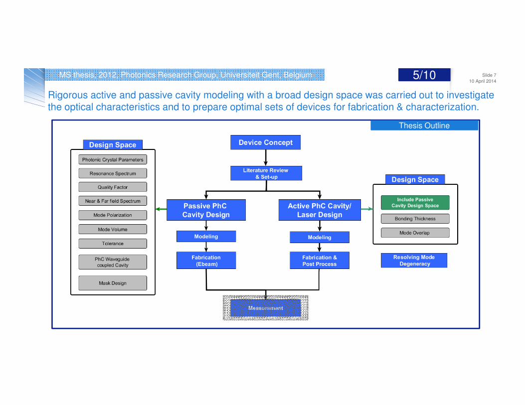
Rigorous active and passive cavity modeling with a broad design space was carried out to investigate the optical characteristics and to prepare optimal sets of devices for fabrication & characterization.
5/10
Thesis Outline

10 April 2014
Slide 8MS thesis, 2012, Photonics Research Group, Universiteit Gent, Belgium 6/10, Passive Cavity
1. Adaptation layers (blue, & green) were introduced between the core & the mirror to allow adiabatic
field transition of the confined band-edge mode. � Increased the Q factor by orders of magnitude.
Photonic Crystal Cavity Layout Field distribution in x, Abrupt field transitions Field distribution in x, smooth field transition
Without Adaptation Layer With Adaptation Layer
A confined band-edge PhC cavity, resonant at 1.54µm with a Q factor of ~22500, can be realized on SOI
within an area of ~235���. It also shows large (~60nm) mode separation.
2. Logarithm of the cavity resonance
spectrum show two additional lossy (low
Q) peaks with 60 and 88nm apart from
the designed high Q, 1540nm resonance
peak.
Their existence can be explained by the
band diagram. Band-edge resonance of
the mirror layer, and confinement of
secondary (M point) band-edge caused
these two additional peaks.
3. Increasing the number of ring (layer) in the
mirror PhC, Q factors can be increased. But it
reaches a saturation limit where Q factor is
determined mainly by the vertical out-of-plane
loss.
Considering this saturation limit, optimal device
footprint estimated 16.5um x 14um with a Q
factor of 22500.

10 April 2014
Slide 9MS thesis, 2012, Photonics Research Group, Universiteit Gent, Belgium
The designed cavity shows good tolerance against PhC size variability. Far field k-space analysis emphasize the need for lattice mismatch consideration into the design space.
Tolerance4. Fourier transform (FT) of the near field (figures below) reveals the presence of two competing
behaviors. Strong confinement ( cavity PhC band-edge positioned well within the band gap of
the mirror PhC ) is associated with enhanced far field pattern due to large lattice mismatch.
Cavity PhC 288nm, Mirror PhC 240nm
Cavity PhC 312nm, Mirror PhC 240nm
Pronounced Far field.
Variation of the Q
factor with the
size variability of
the PhC at core.
Variation of the
resonance
frequency with the
size variability of
the PhC at core.
6. PhC fabrication with tight requirement is challenging.
Design space was optimized to increase the tolerance.
It was estimated that for a size variation 40nm, Q factor
remains within 1 − 2 10�Wavelength shift is also small (~1.7%) for size
variation of 20nm
5. PhC waveguide coupled to PhC cavity was also designed. Q factors in competition with the
coupling distances were estimated.
Q factor and PhC waveguide coupling strength against the waveguide separation from the cavity.
7/10, Passive Cavity

10 April 2014
Slide 10MS thesis, 2012, Photonics Research Group, Universiteit Gent, Belgium
Photonic crystal in presence of III-V bonding layer can sustain band-edge or even confined band-edge resonances. Thinner bonding thickness is necessary to lower the cavity loss (to achieve high Q).
8/10, Active Cavity
Bonding ThicknessInGaAsP/InP quantum well stack with following composition was used. Cavity resonance spectrum was
matched to the peak intensity of the measured emission spectrum of the stack for optimal gain.
Measured emission
spectrum of the III-V
stack.
1. Presence of III-V as the top
cladding distorts the band diagram.
PhC structure exists at the cladding
layer to the III-V active medium, and
only the evanescent component is
influenced by the modulation of the
refractive index in the PhC layer. So,
effective index difference seen by
the hybrid mode at PhC layer is very
small leading to band distortion.Band diagram with III-V top cladding. Detailed band diagram of the highlighted area.
Cavity
resonance
spectrum
Cavity resonance spectrum
at different excitation rangeDetails analysis of the band-edge
surprisingly reveals that band-edge
or even confined band-edge can still
be possible at some hot spots
frequencies (marked with letter)..
2. Resonant spectrum and cavity Q is
quite dependent on the bonding thickness.
The lower the thickness, the higher Q.
This can also be understood from the
effective index consideration.
At low, BCB thickness, effective index
difference in the periodic medium (PhC) is
large compared to the thick BCB layers. It
leads to high Q
BCB thickness has its technical limits
(~100nm). So, thin (~50nm) separation of
the molecular bonding could potentially
improve the cavity performance.
However, at very low (<30nm) or large
(>200) hybrid mode cease to exist. Modes
become localized to either mostly in III-V
or mostly in silicon.

10 April 2014
Slide 11MS thesis, 2012, Photonics Research Group, Universiteit Gent, Belgium 9/10, Active Cavity
Mode overlap & Mode volume
For a nominal device configuration, 52%
mode overlap with III-V is estimated. Mode
overlap or the confinement factor between
the III-V and PhC layer formulated as:
For a nominal device configuration, the
mode volume is relatively small and
estimated to be �. ��(�/�)�
Mode volume V is a quantization volume
encompassing the resonator and with a
boundary in the radiation zone of the cavity
mode under study
The confinement factor helps relating the
amount of interaction the mode has with the
gain material.
� A dipole Gaussian pulse source, placed at the III-V epi-
layer, excites the cavity. Electric field distributions
shown left, and are calculated after sufficient time elapse
ensuring the source and all other low Q modes have
been extinguished.
� The two dominant resonance peak, one at 1.565µmand another at 1.612 µm have found with Q factor of
756 and 558 respectively.
Cavity
resonance
spectrum
Electric field distribution (y component) of the resonant mode at 1.565µm
Detailed band diagram of
the cavity and mirror layer
ensure the possibility for
the confined band-edge
resonance, at marker A
and G (highlighted with
orange shadow)
� Q factors are further optimized by increasing the
number of mirror layers and estimated to be ~1200
with a footprint of 550���
A confined band-edge hybrid III-V/SOI cavity supporting resonance at 1.56µm with a Q factor of ~1200, mode volume of �. ��(�/�)� can be realized with sufficient mode overlap with III-V gain material, and within an area of ~550���. BCB thickness required ~100nm. Photonic crystal
configurations are: triangular lattice with 410nm pitch, core PhC hole size 295nm, mirror PhC hole size 246nm.

10 April 2014
Slide 12MS thesis, 2012, Photonics Research Group, Universiteit Gent, Belgium 10/10
Mask design & Device Processing
Confined band-edge resonance mode at 1.54µm is doubly degenerate. However, by symmetry breaking and careful design, degeneracy can be removed.
� Field distribution, and resonance spectrum with longer
and finer FDTD analysis show the evidence of
degenerate mode due to subtle symmetry breaking.
Resolving Mode Degeneracy
Resonance spectrum; blue colored
spectrum resulted from much longer
duration and finer FDT analysis.
� To resolve the degenerate states, cavity was excited
with multiple symmetry configurations, for example
anti-symmetric in y and symmetric in x, and thus
suppressing the modes that do not have that
particular applied symmetry.
Logarithmic resonance spectrum from the FDTD
analysis with different symmetry configurations.
� Magnetic field distribution of the doublydegenerate mode (left-A2, right-A1) at thedesigned cavity resonance wavelength of 1.54um
� Active devices were patterned on a 220nm (silicon
thickness) SOI wafer with a 193nm DUV immersion
lithography tool. Process was optimized for generic
photonics devices. Active devices were patterned on
a die of a 200mm wafer.
Mask layout for the active devices.
� After post processing the photonic crystal patterned,
SOI die was DVS-BCB (divinylsiloxane-bis-
benzocyclobutene) bonded to III-V stack. Several
aggressive cleaning steps were performed before the
BCB deposition and thermal treatment. Then the III-V
die was bonded with SOI die in a vacuum chamber.
� A second set of
photonic crystal devices
were patterned with
Ebeam for passive
characterization.
� Characterization and
measurement of device
are planned in future,
possibly with a follow-
up work.
10 April 2014
Slide 13MS thesis, 2012, Photonics Research Group, Universiteit Gent, Belgium Conclusion
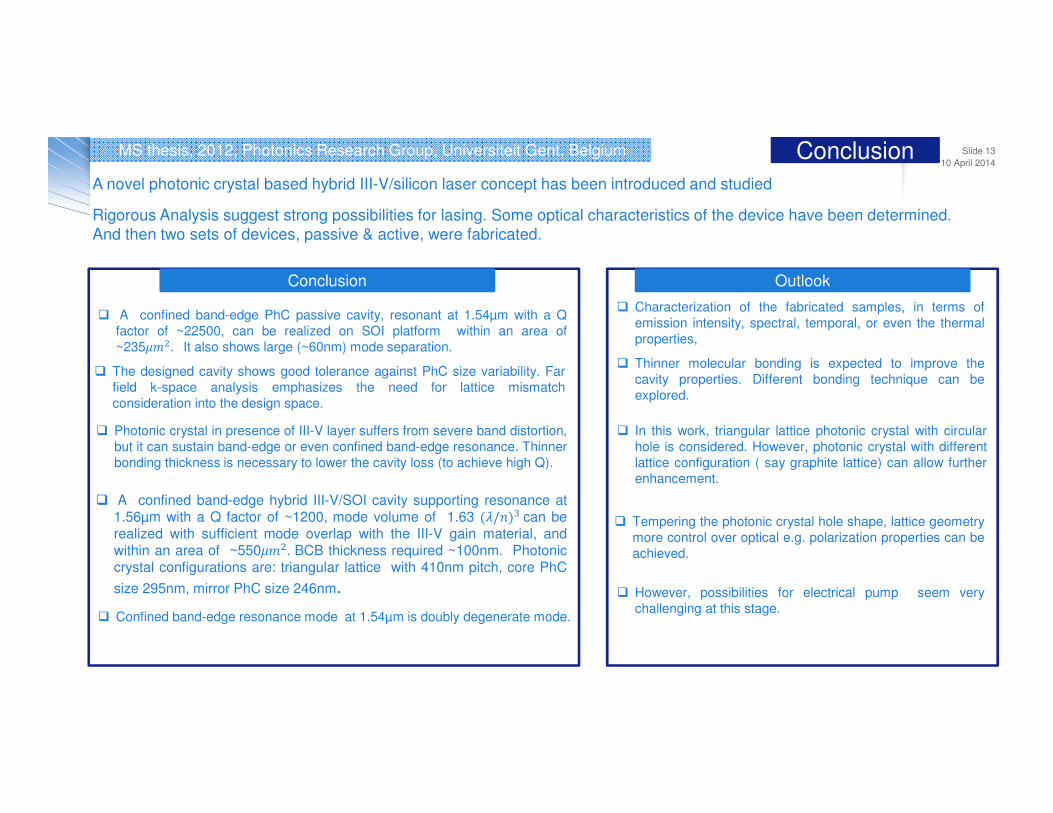
Outlook
A novel photonic crystal based hybrid III-V/silicon laser concept has been introduced and studied
Rigorous Analysis suggest strong possibilities for lasing. Some optical characteristics of the device have been determined. And then two sets of devices, passive & active, were fabricated.
� Characterization of the fabricated samples, in terms of
emission intensity, spectral, temporal, or even the thermal
properties,
� However, possibilities for electrical pump seem very
challenging at this stage.
Conclusion
� Thinner molecular bonding is expected to improve the
cavity properties. Different bonding technique can be
explored.
� In this work, triangular lattice photonic crystal with circular
hole is considered. However, photonic crystal with different
lattice configuration ( say graphite lattice) can allow further
enhancement.
� Tempering the photonic crystal hole shape, lattice geometry
more control over optical e.g. polarization properties can be
achieved.
� A confined band-edge PhC passive cavity, resonant at 1.54µm with a Q
factor of ~22500, can be realized on SOI platform within an area of
~235���. It also shows large (~60nm) mode separation.
� The designed cavity shows good tolerance against PhC size variability. Far
field k-space analysis emphasizes the need for lattice mismatch
consideration into the design space.
� Photonic crystal in presence of III-V layer suffers from severe band distortion,
but it can sustain band-edge or even confined band-edge resonance. Thinner
bonding thickness is necessary to lower the cavity loss (to achieve high Q).
� A confined band-edge hybrid III-V/SOI cavity supporting resonance at1.56µm with a Q factor of ~1200, mode volume of 1.63 (�/�)�can berealized with sufficient mode overlap with the III-V gain material, andwithin an area of ~550���. BCB thickness required ~100nm. Photoniccrystal configurations are: triangular lattice with 410nm pitch, core PhC
size 295nm, mirror PhC size 246nm.
� Confined band-edge resonance mode at 1.54µm is doubly degenerate mode.

10 April 2014
Slide 14MS thesis, 2012, Photonics Research Group, Universiteit Gent, Belgium
Both time domain FDTD and frequency domain plane wave basis electro-magnetic(EM) mode solver were used
to exhaustively model and design the devices.
Extra slide
Effective index based 2D vs 3D analysis.
Carried out modeling required to set-up a computationally expensive simulation server, and even then it takes ~8
hours each simulation run of the 3D model .
Effective index based coarse 2D model was used get initial
estimate for the optimal design space. Then expensive 3D
model was used to fine tune the model.
Detailed band-diagram at the edge Group velocity
One interesting observation, 2D effective index based
simulation underestimate the Q factors which is contrary to
the common belief. It is generally assumed that 2D reports
high Q since it can not incorporate all loss routes (e.g
vertical out-of-plane).
Detail comparison of effective index based 2D vs 3D
simulation shows band-edge are much flatter (low group
velocity near band-edge� high Q) in 3D simulation
compared to the 2D one.
Tools & Set-up.
� FDTD: MIT electromagnetic equation
propagation (MEEP) was used for FDTD
based EM solver. Simulation was
continued for long time to allow sufficient
convergence.
Figure: gradual convergence of the DTFT flux.
Inset: position of the flux planes.
For photonic crystal simulation, Perfectly
Matched Layer (PML), artificial absorbing
layer truncating the computational grid, is
quite critical. Smart PML settings were
used to ensure stable computation.
� MIT photonic band (MPB), a preconditioned block-iterative eigensolver in a
plane wave basis to solve Maxwell equation, was used to calculate the
band diagram.
� Harmonic inversion technique was used to
estimate the cavity Q factor. Figure left, shows
the time response of the cavity. Time marker
was selected such to avoid the transient
responses.

10 April 2014
Slide 15
Infra red photo detector for high power CO2 laser beam profiling and position detector.

10 April 2014
Slide 16Student researcher, 2011, Brussels Photonics Team, Belgium
Design & Realization of infra red photo detector exploiting Seebeck effect for high power CO2 laser.
Photograph of an array (8) of the fabricated IR photo detectors. Yellow box high light a single detector. Contact wires were patterned between the active area and contact pad (red)..
� Conventional (e.g. photo electric) photodetector are
good in term of sensitivity but their performance degrade
strongly at high incident power.
� Seebeck effect based Photo Detector: An incident laser
beam induces temperature distributions inside the p-doped
semiconductor, which leads to a generated voltage owing to
the thermo-electric Seebeck effect.
� Seebeck Photodetector is well-suited for working with
lasers at high optical intensities, a regime in which other
detector options become very limited.
� Monitoring of the spatial intensity profile of the CO2 lasers isquite important in laser-based industrial applications.
� Material processing involving laser ablation is
quadratic to the intensity of the laser beam, whereas
the output intensity of the laser beam is again
quadratic to the beam width.
� So, a small change in beam width can results in much
larger impact on the target.
Rationale
Driver
1/3
Realized Device & Measurement
Dimension of each pixel360x600µm
Dimension of active area of a pixel160x200µm
Contour plot of the detected intensity (avg. power 0.25mW) by the array.
Horizontal axis is the total length of 8 pixel (3.16mm), vertical axis is the
width of the pixel, color represents the detected intensity.
Pixel Separation400µm
Different rows measured bythe corresponding detectorwith a XY translation. (xstep 30µm , y step 50µm)
Detector 4 (from top)was defected.
Each detector consist of activearea, a metal shield and contactwire to the contact pad.

10 April 2014
Slide 17
Measured detectors show ~2.5mV/W sensitivity and linear behavior within the measured range of 0.2-1.2W.
Incident beam: CO2 laser
Operating Principles
2/3
Measurement Setup
� Operates by photon-induced free carrier absorption in doped
semiconductor. Output can be formulated simply by
���� = S∆! where S, effective Seebeck coefficient & ∆T, temperature gradient between two contact
� Seebeck coefficient on extrinsic p-doped semiconductor can be
estimated by
s= "#$ (%�+ '( − )*+),
"#- + .()
where �/ , Boltzmann constant, rscattering parameter, 01 , 02 are
respectively valence and Fermi energy,.( the correction for Fermi-Dirac
statistics & phonon-drag. .
� Temperature dependence of the Fermi level and the band-
edges, and the single carrier scattering mechanism, put
additional driving forces to the carrier and influence the Seebeck
coefficient.
Linearity the photo detector within the operation range. Incident power is in x axis and detected maximum voltage at y axis.
Fig: Schematics of the measurement set-up.
The chopper was used at
35Hz and 305Hz for cross
talk measurement.
Normalized Intensity profile measured
with knife-edge method,
Measured max sensitivity of different pixels. The differences arise from the uncorrected differences in the contact wire resistances due to different position of the detectors.
Sensitivity Linearity
High power CO2 CW was
attenuated with beam splitter
and mechanically chopped
with 50% duty cycle.
Student researcher, 2011, Brussels Photonics Team, Belgium

10 April 2014
Slide 18
1. Cross talk of the detectors was estimated (~ -8.5dB) and it improves at increased lock-in frequency.
Cross talk
3/3
Application: Position Detector
2. Additionally, some detectors were used to design a fourth quadrant on-chip position detector.
Normalized sensitivity distribution across X to show the Thermal cross talk at different lock in frequency.
At 35Hz lock in frequency a side peak appeared at the nearby detector.
� Cross talk depend on the incident laser pulse duration.
� Larger pulse duration allow electron to energyexchange with lattice leading to thermal diffusionand increased cross talk.
� For very short pulse, energized electron canrelaxed quickly and thus follow incident intensity.� low cross talk.
Schematics of the position detector. Red
circle represents the incident beam. Detected voltage contour plot for each of the
quadrant.
34 = 5 5 6�7(8+89):;(<+<9):�=:
>:+(8+89):
?
>;8
?� �@
A = 34 + 3B − (3/ + 3C)(34+3/ + 3C + 3B)
D = 34 + 3/ − (3C + 3B)(34+3/ + 3C + 3B)
Diameter 4800µm
The detector block wasmoved along XY in frontof the a fixed beam.Sweeping was 7mm ineach direction with astep of 200µm
Detected energy in each quadrant can be approximated by
Like wise for other quadrant. Then with some additional steps, the detected X, Y position can be formulated by
X position calibration curve Y position calibration curve
Dete
cte
dX
,Y
sig
nalvs.
the
applie
dX
,Y
transla
tion.
Student researcher, 2011, Brussels Photonics Team, Belgium

10 April 2014
Slide 19
Summer Research: Building a set-up for two photon fluorescence microscopy.

10 April 2014
Slide 20Summer Research, 2011, VTT Technical Research Center of Finland
Built a set-up for two photon florescence microscopy
Driver
1/3
Assembling the components for the microscope (1/2)
Two photon fluorescence principles (collected)
� Two-photon fluorescence microscopy has become a powerful tool
for studying biological functions in live tissue
� Larger (2x) absorption wavelength
allows deep penetration within
tissue, and smaller energy allow
long-term imaging without
compromised tissue viability, or
photo bleaching.
� Common bio proteins have fluorescence
emission far below the excitation
wavelength (1064nm). This allow filtering
the incident beam� unparallel resolution.
Fluorescence spectra of common fluorophores. (VTT)
� Multiple fluorophore can be excited at
the same time. Additional time resolved
features can be added to distinguish
overlapping fluorescence differing
temporal properties.
� Although two photon absorption is less probable, high peak photon
density of recent pulse laser around ~1064nm wavelength increased
the absorption probability by several orders
� Laser: 690ps, Q switched, Nd:YAG microchip laser was used.
� Pilot beam: 532nm, with average power 3mW
� Excitation beam: 1064nm, joule pulses, 690ps pulse
width, average power 1mW, repetition rate 36.2kHz.
� Diode pump at 800nm
� Beam steering: Scanlab dynAxis T Galvano
scanner was used for precise beam steering
through computer interface.
� Beam filtering: Z1064/10x ( Chroma
Tech.) narrow bandwidth transmission
filter around 1064nm was chosen to filter
out the pilot and the pump spectrum.
Transmission profile of the filter, (Chroma Tech.)
� Beam splitter: SemRock Brightline short
pass dichroic beam splitter was chosen
to reflect exciting pulse to the sample &
transmit the fluorescence to microscope.
Transmission profile of the filter (Semrock),
� 99.9% reflection at 1064nm. 93-98%
transmission at 490-746nm window.

10 April 2014
Slide 21Summer Research, 2011, VTT Technical Research Center of Finland
Optical CAD design was performed to estimate the nominal positions of the optics to ensure best focus at image plane and robustness to the mechanical beam steering.
2/3
Assembling the components for the microscope (2/2)
� Microscope: Nikon TS100-F inverted microscope was available at VTT
and used as the basis for set-up.
� Longer working distance and large NA.
� Allow phase contrast microscopy.
� Multi-pixel Photon Counting Module (MPCC):
Two photon fluorescence emission is of very low
intensity. MPCC module was used to improve
the detection. MPCC is made of multiple
avalanche photodiode pixels operating in Geiger
Mode.
MPCC module
� Alternative Image Acquisition: SPOT RTSE
1.39 Mega pixel camera mounted on the Nikon
TS100-F was used as the alternate image
acquisition tools.
� Response range 320-900nm with dark
count 600-1200kcps at 0.5 p.e. threshold.
� Read noise 6-8 e/rms, Dark Noise:
0.012e-/p/s
OptiCAD design of the component optics.
OptiCAD (ray tracing) was used to model the whole set-up to find the
optimal positions of the optics, given to some physical constraint.
Ray tracing model for the
optical path for the set-up.
Best focus at the image plane (1mmx1mm) was ensured for the nominal
distances of the optical set-up.
Nominal position
Focus at Image plane (1mm diameter)
-1.5 deg. Beam steer. Focus blur but still in image plane.
+1.5 deg. Beam steer. Focus blur but still in image plane.

10 April 2014
Slide 22Summer Research, 2011, VTT Technical Research Center of Finland
Set-up was made ready for two-photon fluorescence microscopy. Additional image post processing steps were required.
3/3
The Set-up Sample preliminary detected Image
A well collimated beam from the laser goes though a beam expander, after being attenuated,
to the XY scanner. The scanner reflects the light to a lens with small diameter. The angular
position of the scanner mirror can be adjusted from the PC. Then light is reflected by a 45 deg.
mirror through a lens with large diameter to a cleaning filter which filter out the 532nm pilot
~800nm pump spectrum. Then it is incident on a dichroic filter. 1064nm light gets reflected
from the dichroic to the sample through the microscope objectives and excites the fluorophore.
Then the emitted fluorescence passes through both the objectives of the inverted microscope
and the dichroic filter to the microscope eyepiece or the camera depending on the selected
nob. However, the eyepiece was removed and replaced with the MPCC module.
Sample Table
Exciting beam
(1064nm)
Dichroic
Filter
Fluorescence
to eye piece
Bottom
mirror
Mounted SPOT camera was used to detect somepreliminary images of the focus at image plane.
Photon count detected by the MPCC module.Negative peaks are due to some saturation effect.Data post processing was still required to constructimages from the photon counts.

10 April 2014
Slide 23
BS thesis: Performance optimization of the Erbium doped Silicon Nanocrystal toward the development of silicon laser.

10 April 2014
Slide 24BS thesis, 2009, Dept. of EEE, Bangladesh Univ. of Engineering & Tech. (BUET)
Optimization and prospects of Erbium doped Silicon nano-crystal system in achieving optical amplification & lasing have been studied.
Drivers
1/4
Erbium Doped Silicon Nanocrystal Material
Calculated gate & interconnect delay at different technology node. (Collected)
� Traditional (e.g. Cu) devices interconnect
delay will reach a bottleneck hindering
future node shrinkage.
� Due to indirect band gap, photon emission
in Silicon is phonon mediated process, ,
and thus inefficient, unsuitable for optical
amplification.
E-k diagram of the bulk silicon.
� To overcome this quantum confinement in
silicon (silicon nanocrystal) has been
actively considered. This widen the silicon
band-gap allowing broad absorption range,
increased absorption cross section, and
reduced thermal quenching.
� However, emission from the silicon nano-crystal (Si-nc) are still small and
poor (slow, broad spectrum) compared to direct bandgap III-V material.
In presence of rare earth dopant like Erbium , Si-nc greatly enhance the
erbium luminesce and excitation efficiency. Erbium can emits around
1.54µm wavelength which is low loss optical communication window.
Silicon nanocrystal rich SiO2 containing
Erbium material shows strong energy
coupling between Erbium and Si-nc.
� It’s evident that to maximize Erbium luminescence, Erbium concentration
need to increase.
� On-chip optical interconnect is a promising
solution. The holy grail is the matured
process, like CMOS, compatible optical
source.
Key ChallengesPhotoluminescence of Si-nc and Erbium (3'�;)
at different Erbium concentration measured at
15K, (from Dolf Timmerman).
At increased Erbium concentration,
Si-nc luminescence decreases and
Erbium luminescence increased �
proof that Si-nc energy is non-
radiatively coupled to Erbium
� However, when the number of Erbium ions coupled to a nanocrystal is
increased, the Erbium excitation fraction decrease. Furthermore, at
increased Erbium concentration non-radiative competing process like
excited state absorption, auger recombination detrimentally impact the
output emission.
� Increasing the Silicon nanocrystal and incident pump density help. But
there are technical trade offs, and saturation effect.
So, there is a need for systematically study the complex interplay of
system and to optimize the luminescence characteristics.

10 April 2014
Slide 25BS thesis, 2009, Dept. of EEE, Bangladesh Univ. of Engineering & Tech. (BUET)
Incorporating time and position dependent analytical model the complex interaction of Erbium and Si-nc have been studied for guiding optimized population inversion.
Time Dependent Model (1/2)
2/4
Si-nc acts as strong sensitizer for the erbium. Si-nc absorbs the pumping
photon flux ϕ and generates electron-hole pairs (excitions). The
recombination energy is transferred to the 3'�; ion at ground state to theexcited 6E/� sate. Then it quickly relaxed to the metastable 6F�/� state.
Recombination energy from 6F�/� to ground state is emitted in 1.54µm
radiation. There are finite life times for each interaction.
Based on the previously described interactions, the time dependent rate
equations are modeled as:
Position Dependent Model
Time Dependent Model (2/2)
Schematics of the Erbium and silicon nanocrystal
interaction.
Competing processes, Excited stateabsorption (ESA): absorption of Si-ncrecombination energy by the Erbium at6E/� excited state. Cooperative Up-
conversion: Capture of the 6F�/� to
ground recombination energy byanother 3'�; at 6F�/� to excite itself to
6E/� . Auger Recombination: transfer
back the excited 3'�; at 6F�/�to Si-nc.
Er doping ~1021
density (Ner) (cm-3)τEr 1/420s-1
τPL 4.5ms
Si-nc ~1019
density (Nsi) (cm-3)
Cooperative up conv- 3X10-16
ersion coefficient (Cup ) (cm3s-1)
Si-nc’s absorption ~1X10-16
cross section : σsi.nc (cm2)
Auger deexcitation ~10-19
coefficient (CAug) (cm3s-1)
Radiative lifetime 21µs
(τsi.nc )
ESA coefficient 3X10-19
(cm3s-1)
Coupling Coefficient 3X10-15
C at Nsi=~1019 cm-3 (cm3s-1)
Range of diameter 1.2nm-7.9nm
of Si-nc
Typical value of the modeling parameter determined from the
literatures.
***
.
*
.
*
SiErESASi
o
Er
ncSi
Sio
SincSiSi NNCNCN
NN
dt
dN−−−=
τϕσ
**2**
**
)( SiErAugErup
Er
ErSi
o
ErEr NNCNC
NNCN
dt
dN−−−=
τ
A number of luminescence
properties was determined
by solving these equation
at steady state.
Energy transfer between Si-nc and 3'�; ions is also strongly dependent on
their mutual distance. Thus the coupling coefficient is dependent on both
the density and size of the Si-nc’s. o
nc
R
RR
oeCRC
)(
)(
−−
=
Here, G� is energy transfer coefficient for low fluxes, HIJ is radius of Si-nc and H� is the estimated characteristic distance.
Schematics of the position dependent Erbium
and silicon nanocrystal interaction. Energy ofexcitons is transferred to those 3'�; ions
which are inside the interaction radius (R).
Validation of the position dependent model with the
measurement data from the literature.
10 April 2014
Slide 26BS thesis, 2009, Dept. of EEE, Bangladesh Univ. of Engineering & Tech. (BUET)
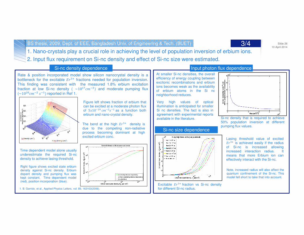
1. Nano-crystals play a crucial role in achieving the level of population inversion of erbium ions.
3/4
At smaller Si-nc densities, the overallefficiency of energy coupling betweenexcitonic recombinations and erbiumions becomes weak as the availabilityof erbium atoms in the Si ncneighborhood reduces.
Figure left shows fraction of erbium thatcan be excited at a moderate photon fluxof 5 10+FEL�+�M+Fas a function botherbium and nano-crystal density.
Rate & position incorporated model show silicon nanocrystal density is a
bottleneck for the excitable 3'�; fractions needed for population inversion.
This finding was consistent with the measured 1.8% erbium excitation
fraction at low Si-nc density ( ~10FOL�+� ) and moderate pumping flux
(~10�?L�+�M+F)reported in Ref 1.
The bend at the high 3'�; density is
due to the competing non-radiativeprocess becoming dominant at highexcited erbium conc.
1. B. Garrido, et al., Applied Physics Letters, vol. 89, 163103(2006).
Right figure shows excited state erbiumdensity against Si-nc density. Erbiumdopant density and pumping flux waskept constant. Time dependent model(red), position incorporation (blue).
Time dependent model alone usuallyunderestimate the required Si-ncdensity to achieve lasing threshold.
Si-nc density that is required to achieve50% population inversion at differentpumping flux values.
Very high values of opticalillumination is anticipated for smallerSi nc densities. The fact is also inagreement with experimental reportsavailable in the literature.
Si-nc density dependence Input photon flux dependence
Si-nc size dependence
2. Input flux requirement on Si-nc density and effect of Si-nc size were estimated.
Excitable 3'�;fraction vs Si-nc densityfor different Si-nc radius.
Lasing threshold value of excited3'�; is achieved easily if the radiusof Si-nc is increased allowingincreased interaction radius. Itmeans that more Erbium ion caneffectively interact with the Si-nc.
Note, increased radius will also affect thequantum confinement of the Si-nc. Thismodel fell short to take that into account.

10 April 2014
Slide 27BS thesis, 2009, Dept. of EEE, Bangladesh Univ. of Engineering & Tech. (BUET) 4/4
� Quantum efficiencies ofthe order of 90% can beachieved forincorporated erbiumdensities of slightlyabove ~10�? L�+�. .
Erbium density values ofthis order has alreadybeen reported in erbiumincorporated Si ncsystems. So it is also apractical estimate.
Contour plot of 50% excited Er fraction atvarious Er and Si-nc density at different pumpingflux. Right side of each curve denotes the regionhaving population inversion over 50%.
1. Nano-crystal densities of the order of the 6 10FQL�+�with erbium incorporation in the range of 10�?L�+�1020 have been found to be resulting in the achievement of population inversion at optical pumping power of the order of 200 mw.
2. High quantum efficiency of energy transfer to erbium atoms has been estimated for erbium densities beyond 10�?L�+�.
Optimized Si-nc, Er and flux density. Quantum Efficiency
� Saturation effect: After ~10�FL�+�M+F fluxdensity saturation effect is observed. Possiblereason is that even if a high pump flux createsmore than one exciton per nanocrystal, only oneof them is capable of transferring therecombination energy to 3'�; in the finite energytransfer time-interval.
� Optimum Pumping: Required Si-nc density foroptical transparency increases abruptly forpumping flux densities of ~5 10FEL�+�M+Forbelow. For pumping with 488nm Argon laser linewith 1mm2 spot-size, that corresponds to a~204mW pump power which is reasonablecompared to typical values (up to 600mW ) usedin the literature.
� Optimum Si-nc density: Incorporation of higherdensities of Si ncs in good quality has itstechnical limits, the recommend value in thiswork is of the order of ~6 10FQL�+�. Thiscorresponds to a reasonable optical pumpingvalue of the order of ~5 10FEL�+�M+F
� Optimum Erbium density: Erbiumdensity can be adjusted in terms of gainrequirements and the design constraintsof the optical cavity for the lasing orwave guiding system.
Calculated quantum efficiency of energy transfer defined as theratio of erbium excitation rate to that of the excitonic recombinationrate in the silicon nano-crystals.
Figure left: Quantum energy transfer efficiency
(given as fraction) at different Er and Si-nc
density where pumping flux is ~5 10FE L�+�M+F
Outlook
� Incorporation of Si-nc density impact on the quantumconfinement
� Electroluminescence of Erbium doped Si-nc can be studied.
� This material in the context of photo detector, and itswaveguiding properties can be studied.

Professional involvements at ASML, the Netherlands.
10 April 2014
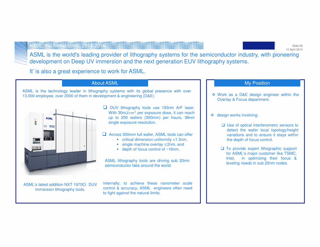
Slide 29ASML, the Netherlands, 2013-2014
About ASML
ASML is the technology leader in lithography systems with its global presence with over
13,000 employee, over 2000 of them in development & engineering (D&E).
� DUV lithography tools use 193nm ArF laser.
With 30mJ/L�� per exposure dose, it can reach
up to 250 wafers (300mm) per hours, 38nm
single exposure resolution.
ASML’s latest addition NXT 1970Ci DUV
immersion lithography tools.
� Across 300mm full wafer, ASML tools can offer
� critical dimension uniformity <1.3nm,
� single machine overlay ≤2nm, and
� depth of focus control of ~16nm,
My Position
� Work as a D&E design engineer within the
Overlay & Focus department.
� Use of optical interferometrc sensors to
detect the wafer local topology/height
variations and to ensure it stays within
the depth of focus control.
� To provide expert lithographic support
for ASML’s major customer like TSMC,
Intel, in optimizing their focus &
leveling needs in sub 20nm nodes.ASML lithography tools are driving sub 20nm
semiconductor fabs around the world.
� design works involving:
Internally, to achieve these nanometer scale
control & accuracy, ASML engineers often need
to fight against the natural limits.
ASML is the world's leading provider of lithography systems for the semiconductor industry, with pioneeringdevelopment on Deep UV immersion and the next generation EUV lithography systems.
It’ is also a great experience to work for ASML.