
Research Article Theoretical Study of One-Intermediate...
11
Research Article Theoretical Study of One-Intermediate Band Quantum Dot Solar Cell Abou El-Maaty Aly 1,2 and Ashraf Nasr 2,3 1 Power Electronics and Energy Conversion Department, Electronics Research Institute (ERI), National Research Centre Building (NRCB), El-Tahrir Street, Dokki, Giza 12622, Egypt 2 Computer Engineering Department, College of Computer, Qassim University, P.O. Box 6688, Buryadah 51452, Saudi Arabia 3 Radiation Engineering Department, NCRRT, Atomic Energy Authority, P.O. Box 29, Nasr City, Egypt Correspondence should be addressed to Abou El-Maaty Aly; [email protected] Received 3 January 2014; Accepted 3 February 2014; Published 24 March 2014 Academic Editor: Xiwang Zhang Copyright © 2014 A.-M. Aly and A. Nasr. is is an open access article distributed under the Creative Commons Attribution License, which permits unrestricted use, distribution, and reproduction in any medium, provided the original work is properly cited. e intermediate bands (IBs) between the valence and conduction bands play an important role in solar cells. Because the smaller energy photons than the bandgap energy can be used to promote charge carriers transfer to the conduction band and thereby the total output current increases while maintaining a large open circuit voltage. In this paper, the influence of the new band on the power conversion efficiency for the structure of the quantum dots intermediate band solar cell (QDIBSC) is theoretically investigated and studied. e time-independent Schr¨ odinger equation is used to determine the optimum width and location of the intermediate band. Accordingly, achievement of maximum efficiency by changing the width of quantum dots and barrier distances is studied. eoretical determination of the power conversion efficiency under the two different ranges of QD width is presented. From the obtained results, the maximum power conversion efficiency is about 70.42% for simple cubic quantum dot crystal under full concentration light. It is strongly dependent on the width of quantum dots and barrier distances. 1. Introduction e intermediate band solar cells (IBSCs) have attracted great attention due to the possibility of exceeding the Shockley- Queisser (SQ) limit [1–4]. From the analysis by Luque et al. [5, 6], the IBSC’s concept yields a maximum theoretical efficiency of 63.2%, surpassing the limit of 40.7% of single gap solar cells under maximum light concentration (the sun being assumed as a blackbody at 6000 K) [7]. Since its introduction in 1997, there have been many theoretical and experimental efforts to explore this idea [8]. e use of quantum dot (QD) technology is proposed as a near term proof of concept of the operating principles of an intermediate band solar cell (IBSC). is intermediate band allows the extra generation of electron-hole pairs through the two-step absorption of subbandgap photons. In the first step, an electron is pumped from the valence band (VB) to the intermediate band (IB), while in the second step, another electron is launched from the IB to the CB [9]. Quantum dot heterojunctions may implement an IBSC because of their ability to provide the three necessary bands [10]. In comparison to conventional quantum well superlattices or multiple quantum well structures, quantum dot superlattice (QDS) that consists of multiple arrays of quantum dots has many advantages due to its modified density of electronic states and optical selection rules. For example, due to relaxed intraband optical selection rules in QDS, they are capable of absorbing normally incident radiation, for example, Indium gallium nitride (In Ga 1− N) alloys feature a bandgap ranging from the near infrared (∼0.7 eV) to ultraviolet (∼3.42 eV); this range corresponds very closely to the solar spectrum, making In Ga 1− N alloys a promising material for future solar cells. In Ga 1− N alloys solar cells have been fabri- cated with different indium contents and the results are encouraging [11]. However, it is not possible in quantum well superlattices. e latter makes QDS a good candidate for infrared photodetector applications [12]. As considered in [13], 3D-ordered QDS with the closely spaced quantum Hindawi Publishing Corporation International Journal of Photoenergy Volume 2014, Article ID 904104, 10 pages http://dx.doi.org/10.1155/2014/904104
Transcript of Research Article Theoretical Study of One-Intermediate...

Research ArticleTheoretical Study of One-Intermediate Band QuantumDot Solar Cell
Abou El-Maaty Aly1,2 and Ashraf Nasr2,3
1 Power Electronics and Energy Conversion Department, Electronics Research Institute (ERI),National Research Centre Building (NRCB), El-Tahrir Street, Dokki, Giza 12622, Egypt
2 Computer Engineering Department, College of Computer, Qassim University, P.O. Box 6688, Buryadah 51452, Saudi Arabia3 Radiation Engineering Department, NCRRT, Atomic Energy Authority, P.O. Box 29, Nasr City, Egypt
Correspondence should be addressed to Abou El-Maaty Aly; [email protected]
Received 3 January 2014; Accepted 3 February 2014; Published 24 March 2014
Academic Editor: Xiwang Zhang
Copyright © 2014 A.-M. Aly and A. Nasr. This is an open access article distributed under the Creative Commons AttributionLicense, which permits unrestricted use, distribution, and reproduction in any medium, provided the original work is properlycited.
The intermediate bands (IBs) between the valence and conduction bands play an important role in solar cells. Because the smallerenergy photons than the bandgap energy can be used to promote charge carriers transfer to the conduction band and therebythe total output current increases while maintaining a large open circuit voltage. In this paper, the influence of the new bandon the power conversion efficiency for the structure of the quantum dots intermediate band solar cell (QDIBSC) is theoreticallyinvestigated and studied.The time-independent Schrodinger equation is used to determine the optimumwidth and location of theintermediate band. Accordingly, achievement of maximum efficiency by changing the width of quantum dots and barrier distancesis studied. Theoretical determination of the power conversion efficiency under the two different ranges of QD width is presented.From the obtained results, the maximum power conversion efficiency is about 70.42% for simple cubic quantum dot crystal underfull concentration light. It is strongly dependent on the width of quantum dots and barrier distances.
1. Introduction
The intermediate band solar cells (IBSCs) have attracted greatattention due to the possibility of exceeding the Shockley-Queisser (SQ) limit [1–4]. From the analysis by Luque etal. [5, 6], the IBSC’s concept yields a maximum theoreticalefficiency of 63.2%, surpassing the limit of 40.7% of singlegap solar cells under maximum light concentration (thesun being assumed as a blackbody at 6000K) [7]. Sinceits introduction in 1997, there have been many theoreticaland experimental efforts to explore this idea [8]. The useof quantum dot (QD) technology is proposed as a nearterm proof of concept of the operating principles of anintermediate band solar cell (IBSC). This intermediate bandallows the extra generation of electron-hole pairs throughthe two-step absorption of subbandgap photons. In the firststep, an electron is pumped from the valence band (VB) tothe intermediate band (IB), while in the second step, anotherelectron is launched from the IB to the CB [9]. Quantum
dot heterojunctions may implement an IBSC because oftheir ability to provide the three necessary bands [10]. Incomparison to conventional quantum well superlattices ormultiple quantum well structures, quantum dot superlattice(QDS) that consists of multiple arrays of quantum dots hasmany advantages due to its modified density of electronicstates and optical selection rules. For example, due to relaxedintraband optical selection rules in QDS, they are capable ofabsorbing normally incident radiation, for example, Indiumgallium nitride (In
𝑥Ga1−𝑥
N) alloys feature a bandgap rangingfrom the near infrared (∼0.7 eV) to ultraviolet (∼3.42 eV);this range corresponds very closely to the solar spectrum,making In
𝑥Ga1−𝑥
N alloys a promising material for futuresolar cells. In
𝑥Ga1−𝑥
N alloys solar cells have been fabri-cated with different indium contents and the results areencouraging [11]. However, it is not possible in quantumwell superlattices. The latter makes QDS a good candidatefor infrared photodetector applications [12]. As consideredin [13], 3D-ordered QDS with the closely spaced quantum
Hindawi Publishing CorporationInternational Journal of PhotoenergyVolume 2014, Article ID 904104, 10 pageshttp://dx.doi.org/10.1155/2014/904104

2 International Journal of Photoenergy
dots and high quality interfaces allow a strong wave functionoverlap and the formation of minibands. In such structures,the quantum dots play a similar role to that of atoms inreal crystals. To distinguish such nanostructures from thedisordered multiple arrays of quantum dots, we refer to themas quantum dot supracrystals (QDC). Other assumptionsthat include the rules for solving the Schrodinger equationfor determining the IBs are considered in the followingsections. The remainder of the paper is organized as follows.In Section 2, the basic assumptions and a superlattice modeldescription are presented.The intermediate band energy andwavevectors of a charge carrier are calculated in Section 3.The induced photocurrent density and power conversionenergy are described in Section 4. The numerical resultsand discussions are summarized in Section 5. Finally, aconclusion of the results is outlined in Section 5.
2. Basic Assumptions and SuperlatticeModel Description
In this paper, the investigations are devoted to one interme-diate band solar cell. We explain the various behaviors of thismodel depending on the QD solar cell parameters, such asquantum dot size, interdot distance, and type of compositionalloy. Meanwhile, in the next step, the multi-intermediatebands are investigated. Therefore, the following are the basicassumptions that are used in the QD one intermediate bandsolar cell model [11–14].
(a) The solar cell model is thick enough; carrier mobilitywill be high enough to ensure the full absorption ofphotons. All photons with energy greater than thelowest energy gap in the QDIBS model are absorbed.
(b) The quasi-Fermi energy levels which are equivalent toinfinite carrier mobility are constant throughout themodel.
(c) The transitions occurring between the bands are onlyradiative recombination.
(d) The solar cell absorbs blackbody radiation at a suntemperature, 6000K, and the temperature of the solarcell, 300K, and emits blackbody radiation at 300Konly.
(e) No carriers can be extracted from the intermediateband; the net pumping of electrons from the VB tothe IB must equal the net pumping of electrons fromthe IB to the CB.
(f) The shape of the QDs is cubic and they must bearranged in a periodic lattice in order to establishwell-placed intermediate band boundaries. For sim-plicity, the energy corresponding to the top of thevalence band is the same both in the barrier and theQDmaterial; therefore there is no valence band offsetand only confining potential occurs at the conductionband offset.
(g) The intermediate band should be approximately half-filled with electrons in order to receive electrons fromthe valence energy band and pump electrons to theconduction energy band.
When charge carriers in semiconductors can be confinedby potential barriers in three dimensions, it is called quantumdots. QDs periodic arrays from semiconductor with a smallerbandgap are sandwiched between two layers of anothersecond semiconductor having a larger bandgap (n or p type).This configuration creates the potential barriers. Two poten-tial wells are formed in this structure; one is for conductionband electrons and the other for valence band holes. Thewell (QDs layer) depth for electrons is called the conductionband offset, which is the difference between the conductionband edges of the well and barrier semiconductors. The welldepth for holes is called the valence band offset. If the offsetfor either the conduction or valence bands is zero, then onlyone carrier will be confined in a well. In this structure, if thebarrier thickness between adjacent wells prevents significantelectronic coupling between the wells, then each well iselectronically isolated. On the other hand, if the barrierthickness is sufficiently thin to allow electronic couplingbetween wells, then the electronic charge distribution canbecome delocalized along the direction normal to the welllayers, therefore producing new minibands (see Figure 1).
The electronic coupling rapidly increases with decreasingthe barrier thickness and miniband formation is very strongbelow 2 nm [15]. Superlattice structures yield efficient chargetransport normal to the layers because the charge carriers canmove through the minibands. As a result the barrier will benarrower and the miniband and the carrier mobility will bewider and higher, respectively.
3. Wavevectors of a Charge Carrier
The wavevector of a charge carrier (single electron or hole)can be described by the time-independent Schrodinger equa-tion, which has the following form [11, 16]:
(−ℎ2
2𝑚∇2
+ 𝑉)𝑘 = 𝐸𝑘, (1)
where ℎ is the Plank’s constant,𝑚 is the effective mass, ∇2 is asecond order differential operator, 𝑉 is the potential energy,𝐸 is the total energy of charge carrier, and 𝑘 is the wavevector.The Kronig-Penney model solved this equation by the one-dimensional periodic potential shown also in Figure 1.
This model assumes that the wave travelling of chargecarrier is in the positive 𝑥 direction for one-dimensional only.Therefore, the mathematical form of the repeating unit of thepotential is
𝑉 (𝑥) = {𝑉0, for 𝑥 = 𝐿
𝐵,
0, for 𝑥 = 𝐿QD.(2)
Here,𝑉0is the conduction band offset,𝐿
𝐵is the barrier width,
and 𝐿QD is the quantum dot width. The period 𝑇 of the

International Journal of Photoenergy 3
Minibands
V0
T
LB
V(x)x
ne = 3ne = 2ne = 1
nh = 1nh = 2nh = 3
LQD
Figure 1: Minibands formation in the superlattice structure and Kronig-Penney potential.
considered potential is equal to (𝐿QD + 𝐿𝐵). The Schrodinger
equation for this model is [10, 17, 18].Consider
𝑑2𝑘
𝑑𝑥2+
2𝑚𝐸
ℎ2𝑘 = 0, for 𝑥 = 𝐿QD, (3a)
𝑑2
𝑘
𝑑𝑥2+
2𝑚 (𝐸 − 𝑉0)
ℎ2𝑘 = 0, for 𝑥 = 𝐿
𝐵. (3b)
According to the Kronig-Penney model, the solution of (3a)and (3b) can be expressed as
𝜎2 − 𝛿2
2𝜎𝛿sinh (𝜎𝐿
𝐵) sin (𝛿𝐿QD) − cosh (𝜎𝐿
𝐵) cos (𝛿𝐿QD)
= cos (𝐿𝐵+ 𝐿QD) 𝑘.
(4)
For simplicity, one can assume the following symbols forinternal terms in (4):
𝜎2
=2𝑚𝐵(𝑉0− 𝐸)
ℎ2=
2𝑚𝐵𝑉0
ℎ2(1 − 𝜖) ,
𝛿2
=2𝑚𝑄𝑉0
ℎ2𝐸
𝑉0
=2𝑚𝑄𝑉0
ℎ2𝜖, 𝜖 =
𝐸
𝑉0
,
(5)
where 𝑚𝐵, 𝑚𝑄
are effective mass of electron in barrierregion and effective mass of electron in quantum dots region,respectively.
Therefore, from (4), the factor into the first term playsan important role for investigating this proposed QDIBSCmodel. It can be expressed as follows:
𝜎2 − 𝛿2
2𝜎𝛿=
𝑚𝑄
− (𝑚𝑄
+ 𝑚𝐵) 𝜖
2(𝑚𝑄𝑚𝐵𝜖)1/2
(𝜖 − 1)1/2
. (6)
Furthermore, the other arguments in (4) for hyperbolic andsinusoidal functions can be defined as
𝜎𝐿𝐵
= 𝜇𝐴𝐵(1 − 𝜖)
1/2
, 𝛿𝐿QD = 𝐴𝑄𝜖1/2
,
𝜇 =𝐿𝐵
𝐿QD, 𝐴
𝐵= 𝐿QD(
2𝑚𝐵𝑉0
ℎ2)1/2
,
𝐴𝑄
= 𝐿QD(2𝑚𝑄𝑉0
ℎ2)
1/2
.
(7)
Substituting these definitions into (4), it will become as
𝑚𝑄
− (𝑚𝑄
+ 𝑚𝐵) 𝜖
2(𝑚𝑄𝑚𝐵𝜖)1/2
(1 − 𝜖)1/2
sinh [𝜇𝐴𝐵(1 − 𝜖)
1/2
] sin (𝐴𝑄𝜖1/2
)
+ cosh [𝜇𝐴𝐵(1 − 𝜖)
1/2
] cos (𝐴𝑄𝜖1/2
)
= cos [𝑘𝐿QD (1 + 𝜇)] , for 𝜖 < 1,
(8a)
𝑚𝑄
− (𝑚𝑄
+ 𝑚𝐵) 𝜖
2(𝑚𝑄𝑚𝐵𝜖)1/2
(𝜖 − 1)1/2
sin [𝜇𝐴𝐵(𝜖 − 1)
1/2
]
× sin (𝐴𝑄𝜖1/2
) + cos [𝜇𝐴𝐵(𝜖 − 1)
1/2
] cos (𝐴𝑄𝜖1/2
)
= cos [𝑘𝐿QD (1 + 𝜇)] , for 𝜖 > 1,
(8b)
cos𝐴𝑄
−𝜇𝐴𝐵
2sin𝐴𝑄
= cos [𝑘𝐿QD (1 + 𝜇)] ,
for 𝜖 = 1.
(8c)
The left-hand side of (8a), (8b), and (8c) can be representedby 𝐹(𝜖) for all values of the ratio of total energy of electronsover conduction band offset: (𝜖 = 𝐸/𝑉
0). Consider
𝐹 (𝜖) = cos [𝑘𝐿QD (1 + 𝜇)] . (9)
Equation (9) cannot be solved analytically, but it can be solvedgraphically. Figure 2 shows the left-hand side of (9), 𝐹(𝜖),against 𝜖 at fixed values of 𝜇 and 𝐴. The concerned QDIBSCmodel depends on the considered alloys in previous studiesfor comparing the results; the quantum dot width: 𝐿QD =
4.5 nm (InAs0.9N0.1, 𝑚𝑄
= 0.0354𝑚0), barrier width: 𝐿
𝐵=
2 nm (GaAs0.98
Sb0.02
,𝑚𝐵
= 0.066𝑚0), and 𝑉
0= 1.29 eV [12].
But in further studies, other alloys will be processed.The left-hand side is not constrained to ±1 and is a function of energyonly.The right-hand side is constrained to a range of±1 and isa function of 𝑘 only.The limits of the right-hand side±1 occurat 𝑘 = 0 to (±𝜋/𝑇). The two horizontal red lines in Figure 2represent the two extreme values of cos[𝑘𝐿QD(1 + 𝜇)]. Theonly allowed values of 𝐸 are those for which 𝐹(𝜖) lies betweenthe two horizontal red lines; see Table 1.
Figure 2 and Table 1 show the allowed energy ranges orbands, 𝐸, which fall into continuous regions separated by

4 International Journal of Photoenergy
Table 1: The allowed energy ranges or bands as 𝐸 for the proposedcomposition from Figure 2.
Band Range of 𝐸, (eV)1 0.2039–0.23692 0.8140–0.98523 1.6638–2.27754 2.4758–3.5439
F(𝜖)
k = 0
𝜖
3
2
1
0
−1
−2
−30 0.5 1 1.5 2 2.5 3
Forbidden energy ranges(i.e., electrons cannot propagate)
Bands or allowed energy ranges
k = ±𝜋
T
Figure 2: The left-hand side of (9), (𝜖), against 𝜖 at fixed values of𝜇 and 𝐴. This graph shows allowed and forbidden electron energybands for the simple cubic QD with the quantum dot width 𝐿QD =
4.5 nm (InAs0.9N0.1, 𝑚𝑄
= 0.0354𝑚0), barrier width 𝐿
𝐵= 2 nm
(GaAs0.98
Sb0.02
, 𝑚𝐵= 0.066𝑚
0), and 𝑉
0= 1.29 eV.
gaps.This distribution of allowed energies illustrates the bandstructure of crystalline solids. According to Figure 2 andTable 1, when the values of 𝐸 are from 0 to 0.2039 eV, 𝐹(𝜖) isgreater than one and so there is no real value of 𝑘 that satisfies(9). At 𝐸 = 0.2039 eV the wavevector will be equal to zero. As𝐸 varies from 0.2039 eV to 0.2369 eV, cos[𝑘𝐿QD(1+𝜇)] variesfrom +1 to −1 and 𝑘𝐿QD(1 + 𝜇) varies from 0 to (±𝜋). As 𝐸
varies from 0.2369 eV to 0.8140 eV, there is no real value of 𝑘that satisfies (9). At 𝐸 = 0.8140 eV, the argument of the right-hand side, 𝑘𝐿QD(1+𝜇), will be equal to (𝜋).At 𝐸 = 0.9852 eV,the argument of the right-hand side, 𝑘𝐿QD(1 + 𝜇), will beequal to (2𝜋). Other bandgaps will periodically appear withthe same behavior.
Figure 3 shows the allowed energy bands and thewavevector states in one-dimensional crystal with the samedata as in Figure 2. In this case, the wavevector is changedfrom 0 to (±𝜋/𝑇), and the allowed energy bands into theelectron energy is assigned. Also, the curve shows thatthe slope (𝑑𝐸/𝑑𝑘) is zero at the 𝑘 boundaries (i.e., 0 and±𝜋/𝑇). Thus, the velocity of the electrons approaches zeroat the boundaries. This means that the electron trajectoryor momentum is confined to stay within the allowable 𝑘.Figure 4 denotes more explanation for the considered energyallowed bands as in Figure 3. It shows the allowed 𝐸-𝑘 stateswith the bandgaps that appear when 𝑘 = 𝑁𝜋/𝑇. The
3.5
3
2.5
2
1.5
1
0.5
00 𝜋/T
k (nm−1)
Elec
tron
ener
gy (e
V)
1 cycle [0 − 𝜋
T]
Band 4
Band 3
Band 2
Band 1
Figure 3: Allowed 𝐸-𝑘 states in one-dimensional crystal with thesame data in Figure 2.
3.5
3
2.5
2
1.5
1
0.5
00 𝜋/T 2𝜋/T 3𝜋/T 4𝜋/T
k (nm−1)
Elec
tron
ener
gy (e
V)
Free electron energy
Figure 4: Allowed 𝐸-𝑘 states and free electrons energy.
dashed line represents 𝐸-𝑘 states for free electrons energy.It can be obtained by letting 𝑉
0= 0 in (4). Therefore,
the free energy of electron is 𝐸 = ℎ2𝑘2/2𝑚. After theessential equations and assumptions are demonstrated, thefollowing section is concerned with the determination of theeffect of intermediate band, alloy construction, and dot andbarrier width in each of induced photocurrent density andcorresponding power efficiency.
4. Induced Current Density and PowerConversion Efficiency
The photon generated current density in QDIBSC withone intermediate band is derived in this section. Then, thesensitivity of the power conversion efficiency as a functionof the intermediate band energy level will be investigated.According to the assumptions in Section 2, the only radiativetransitions occur between the bands therefore the generation

International Journal of Photoenergy 5
CB
IB
VBMaterial II Material IIMaterial I
Δ1
V0pCI pCV
pIV
ECIECV
EIV
EFC
EFI
EFV
Figure 5: Construction of energy band diagram for two semicon-ductor materials (material I; InAs
0.9N0.1: quantum dot, material II;
GaAs0.98
Sb0.02
: barrier width) to create a heterostructure for oneintermediate band solar cell.
0.04
0.03
0.02
0.01
04 4.5 5 5.5 6 6.5 7
QD width at different values of barrier width (nm)
Inte
rmed
iate
ban
d w
idth
Δ1
(eV
)
Barrier width:2 (nm)2.5 (nm)3 (nm)
Figure 6: Change width of intermediate band (Δ1) with change QD
width for the first allowable range at three different values of barrierwidth.
and recombination events are represented by photon absorp-tion and emission. Figure 5 illustrates the construction of anenergy band diagram for a heterostructure in the case ofone intermediate band solar cell. An electron in the valenceband can be excited to either the intermediate or conductionband. Also, an electron in the intermediate band can beexcited to the conduction band. Therefore, there are threeupward energy transitions: 𝐸VI, 𝐸CI, and 𝐸CV. 𝐸VI representsvalence to intermediate band, 𝐸CI represents intermediateto conduction band, and 𝐸CV represents the conventionalbandgap between the valence and conduction band. The twointermediate transitions 𝐸VI and 𝐸CI are independent of eachother, while the bandgap transition 𝐸CV is a function of thetwo intermediate ones: 𝐸CV = 𝐸VI + 𝐸CI.
The photon flux density,𝑁, is the number of photons persecond per unit area per unit wavelength and behaves like
a blackbody flux density and according to the Roosbroeck-Shockley equation [19–22] is given by
𝑁(𝐸VI, 𝐸CI, 𝑇, 𝑝) =2𝜋𝜉
ℎ3𝐶2∫𝐸CI
𝐸VI
𝐸2𝑑𝐸
𝑒(𝐸−𝑝)/𝑘𝐵𝑇 − 1, (10)
where 𝑇 is the temperature, 𝜉 is geometric factor, ℎ is Plankconstant, 𝑘
𝐵is Boltzmann constant, 𝐶 is speed of light, and
𝑝 is chemical potential. To simplify the analysis, assume that𝐸VI ≤ 𝐸CI ≤ 𝐸CV. Therefore the photons with energygreater than 𝐸VI and less than 𝐸CI are absorbed and electronstransfer from valence band to intermediate band and leaveholes in the valence band. Any excess energy greater than𝐸VI and less than 𝐸CI will be lost due to thermalization andcarriers will relax to the band edges before another radiativeoccurs. One can notice that this thermalization value isvery small in comparison with its value in the case of bulkbased semiconductor solar cells.Thismeans that an absorbedphoton with energy greater than𝐸VI and less than𝐸CI has thesame effect as an absorbed photon with energy equal to 𝐸VI.
Photons with energy greater than 𝐸CI and less than 𝐸CVare absorbed and an electron transfers from intermediateband to conduction band. The excess energy behavior hasthe same effect as considered in the previous case regardingthe difference in the transition band process. Photons withenergy greater than 𝐸CV are absorbed and an electrontransfers from valence band to conduction band and createsa hole in the valence band.The absorbed photon with energygreater than 𝐸CV has the same effect as an absorbed photonwith energy equal to 𝐸CV taking into account the excessenergy process.The net photon flux is equal to the number ofcharge carrier flux collected at the contact. When the chargecarrier flux is multiplied by the electric charge of electron, 𝑞,the current density of the QDIBSC for one intermediate bandis [11, 13, 14]:
𝑗 = 𝑞 {[𝐶𝑓𝜉𝑁 (𝐸CV,∞, 𝑇
𝑠, 0)
+ (1 − 𝐶𝑓𝜉)𝑁 (𝐸CV,∞, 𝑇
𝑎, 0)
−𝑝𝑁 (𝐸CV,∞, 𝑇𝑎, 𝑞𝑉) ]
+ [𝐶𝑓𝜉𝑁 (𝐸CI, 𝐸CV, 𝑇𝑠, 0)
+ (1 − 𝐶𝑓𝜉)𝑁 (𝐸CI, 𝐸CV, 𝑇𝑎, 0)
−𝑁 (𝐸CI, 𝐸CV, 𝑇𝑎, 𝑝CI) ]} ,
(11)
where 𝐶𝑓is concentration factor, 𝑇
𝑠is temperature of sun
(6000K), 𝑇𝑎is ambient temperature (300K), 𝑞𝑉 is quasi-
Fermi energy, and 𝑝CI is chemical potential between conduc-tion and intermediate bands. The terms in the first bracketrepresent the current density generated when the electronstransfer from the valence band to the conduction band astypically for conventional solar cell. While the terms in thesecond bracket represent the current density generated whenthe electrons transfer from the intermediate band to theconduction band. In both bracketed terms, the QDIBSCabsorbs radiation from the sun at the temperature 𝑇
𝑠and

6 International Journal of Photoenergy
0.55
0.5
0.45
4 4.5 5 5.5 6 6.5 7
Barrier width:
QD width at different values of barrier width (nm)
2 (nm)2.5 (nm)3 (nm)
Ener
gy g
ap b
etw
een
VB
and
IB (e
V)
(a)
4 4.5 5 5.5 6 6.5 7
1.15
1.1
1.05
QD width at different values of barrier width (nm)
Barrier width:2 (nm)2.5 (nm)3 (nm)
Ener
gy g
ap b
etw
een
IB an
d CB
(eV
)
(b)
Figure 7: (a) Change energy gap between VB and IB according to change in QD width for the first allowable range at different values ofbarrier width. (b) Change energy gap between IB and CB with the same conditions in (a).
𝑇𝑎, respectively, while it emits radiation at the temperature
𝑇𝑎and a corresponding chemical potential. The current
density of the QDIBSC is formulated according to theproper operation of the QDIBSC which requires that thereis no current extracted from the intermediate band; that is,the current entering the intermediate band must equal thecurrent leaving the intermediate band. Therefore, the secondterm in (11) can be rewritten as [14, 23, 24]
𝑞 [𝐶𝑓𝜉𝑁 (𝐸CI, 𝐸CV, 𝑇𝑠, 0) + (1 − 𝐶
𝑓𝜉)
× 𝑁 (𝐸CI, 𝐸CV, 𝑇𝑎, 0) − 𝑁 (𝐸CI, 𝐸CV, 𝑇𝑎, 𝑝CI) ]
= 𝑞 [𝐶𝑓𝜉𝑁 (𝐸VI, 𝐸CI, 𝑇𝑠, 0) + (1 − 𝐶
𝑓𝜉)
× 𝑁 (𝐸VI, 𝐸CI, 𝑇𝑎, 0) − 𝑁 (𝐸VI, 𝐸CI, 𝑇𝑎, 𝑝IV) ] .
(12)
The output voltage can be described as the difference of thechemical potentials betweenCBandVB; that is, 𝑞𝑉oc = 𝑝CV =
𝑝CI + 𝑝IV.In this work, the light intensity on QDIBSC is calculated
by the number of suns, where 1 sun (or concentration factor𝐶𝑓
= 1) means the standard intensity at the surfaceof the Earth’s atmosphere. Therefore, at the surface of theEarth’s atmosphere the power density falling on a QDIBSCis 𝑃in = 𝜉𝜎
𝑠𝑇4𝑠
= 1587.2w/m2, where 𝜎𝑠is Stefan’s constant
and 𝑇s is temperature of sun (6000K). Theoretically, thefull concentration would be achieved when 𝐶
𝑓= 1/𝜉 =
46296. The power conversion efficiency, 𝜂, of the QDIBSC isdependent on𝑃in, so that it varies with the level concentrationof 𝐶𝑓. We concentrate our study on the QDIBSC efficiencies
with unconcentrated light 𝐶𝑓
= 1 and also compared it withfull concentration light 𝐶
𝑓× 𝜉 = 1. The power conversion
efficiency equation of the QDIBSC is
𝜂 =𝑉oc × 𝐽SC × 𝐹𝐹
𝑃in=
𝐽𝑚
× 𝑉𝑚
𝐶𝑓𝜉𝜎𝑠𝑇4𝑠
=𝐽𝑚
× 𝑉𝑚
𝐶𝑓× 1587.2
, (13)
where 𝑉oc is open circuit voltage, 𝐽sc is short circuit currentdensity, 𝐹𝐹 is fill factor, 𝑉
𝑚is maximum voltage of the
QDIBSC, and 𝐽𝑚ismaximumcurrent density of theQDIBSC.
After mathematical concepts and assumptions are definedin previous sections for assigned composition of material,the following section reports some features of the QDIBSCsperformance for one intermediate band case.
5. Numerical Results and Discussions
The discussion firstly starts by manifesting the relationbetween QDIBSC parameters and the distribution of IBenergies in the gap between valence and conduction bands.When the Schrodinger equation (1) is solved, many solutionsare obtained. Some of them can be satisfied but others cannot.From the satisfied solutions, there are multi-intermediatebands as pointed from Figures 2, 3, and 4.They are essentiallydependent on QDIBSC parameters such as QD, barrierwidths. Here, we are concerned only with the effect of thefirst intermediate band, IB, into the behavior of the proposedmodel. From the obtained results, we found two ranges ofquantum dot widths that vary the positions of intermediatebands. Other ranges of quantum dot widths will denoteunachievable behavior. In the following discussions, theenergy distributions, 𝐽-𝑉 characteristics, and correspondingpower conversion efficiency are studied for each range. Com-parisons between the two ranges outcomes are processed. Asummary of all the related values describing the model isconsidered in Table 2. For the first range (QD width changesfrom 4–7 nm), the dependence of first intermediate bandwidth,Δ
1, onQDwidth at different barrier widths is depicted
in Figure 6. One can recognize that the width of IB, Δ1, is
decreased with an increase in the QD width. This behavior isconsistent with the previous investigations that demonstratethat the decreasing of Δ
1IB will assist in the fall down of the
power conversion efficiency, as will be described later [11, 14].Also the same trend will be found in the second range ofQD and barrier widths, which also denotes the first IB. Also,Figure 6 illustrates that when the barrier width increases in

International Journal of Photoenergy 7
Table 2: Three different values of QD width (InAs0.9N0.1) and barrier width (GaAs0.98Sb0.02) for two different ranges of QD available widthsat full concentration and unconcentration.
Two availableranges
Parameters Full concentration Unconcentration𝐿QD(nm)
𝐿𝐵
(nm)𝜂max(%)
𝑉max(v)
𝐽max × 𝜉
(mA/cm2)
𝑉o𝑐 (v)𝐽sc × 𝜉
(mA/cm2)
FF 𝜂max(%)
𝑉max(v)
𝐽max(mA/cm2
)
𝑉oc(v)
𝐽sc(mA/cm2
)FF
“1st range”4–7 nm
4 2 63.2 1.503 66.8 1.57 67.9 0.942 51.6 1.231 66.5 1.33 67.9 0.9064.5 2 61.2 1.505 64.6 1.58 65.6 0.938 50.0 1.233 64.3 1.34 65.6 0.9025 2 59.6 1.507 62.8 1.58 63.8 0.939 48.7 1.235 62.5 1.34 63.8 0.9034 2 63.2 1.503 66.8 1.57 67.9 0.942 51.6 1.231 66.5 1.33 67.9 0.9064 2.5 63.1 1.514 66.2 1.58 67.3 0.943 51.6 1.242 65.9 1.34 67.3 0.9084 3 63.0 1.516 65.9 1.58 67.0 0.944 51.5 1.244 65.7 1.35 67.0 0.904
“2nd range”7–11 nm
8.1 1.98 70.4 1.508 74.1 1.57 75.3 0.945 57.5 1.238 73.7 1.34 75.3 0.9048.6 1.98 68.4 1.510 71.9 1.57 73.1 0.946 55.9 1.238 71.6 1.34 73.1 0.9059.1 1.98 66.7 1.512 70.0 1.58 71.2 0.941 54.5 1.241 69.8 1.34 71.2 0.9088.1 1.98 70.4 1.508 74.1 1.57 75.3 0.945 57.5 1.238 73.7 1.34 75.3 0.9048.1 2.48 70.3 1.519 73.4 1.58 74.7 0.945 57.5 1.248 73.1 1.35 74.6 0.9068.1 2.98 70.2 1.522 73.2 1.59 74.4 0.942 57.4 1.250 72.9 1.35 74.4 0.907
0.04
0.035
0.03
0.025
0.02
0.015
0.01
0.005
08.5 9 9.5 10 10.5 11
Inte
rmed
iate
ban
d w
idth
Δ1
(eV
)
QD width at different values of barrier width (nm)
Barrier width:1.98 (nm)2.34 (nm)2.7 (nm)
Figure 8: Change width of intermediate band (Δ1) with change
QD width for the second allowable range at three different valuesof barrier width.
the allowable range (2-3 nm), Δ1IB somewhat increases. At
the same time, the increase of barrier width will somewhatinversely decrease the energy gap between IB width and eachof VB and CB, as this behavior is shown in Figures 7(a) and7(b). It is expected that when Δ
1IB enlarges, the energy gap
difference between it and the considered VB and CB will bedecreased, as the total distance 𝐸cv is constant [11, 14]. Thefirst range power efficiency and 𝐽-𝑉 characteristics will becompared with the second range in the last part of thesediscussions.
For the second allowable range (QD width changes from8.1–9.1 nm) and at the same barrier width range (2-3 nm),the intermediate band width, Δ
1, with QD width at different
values of barrier width is considered in Figure 8. Whencomparing this figure with the previous Figure 6, they gavethe same trend. On the other hand, the varying Δ
1in the
first range covers a longer range of energy in comparisonwith the second one. Moreover, the allowable barrier widthrange in this second range is shifted left to be from 1.98 nmto 2.7 nm. The energy gap between the IB and each of VBand CB is illustrated in Figures 9(a) and 9(b). As a result ofchanging the values ofΔ
1, the corresponding values of energy
gaps will be changed for the composition of the model, QDwidth (InAs
0.9N0.1) and barrier width (GaAs
0.98Sb0.02
). Alsothe curves in this case tend to be straight in comparison withtheir equivalent in Figures 7(a) and 7(b). One can notice thatthe second range investigations were not considered before inprevious studies. Although it gives an enhancement of powerconversion efficiency as shown in the next results.
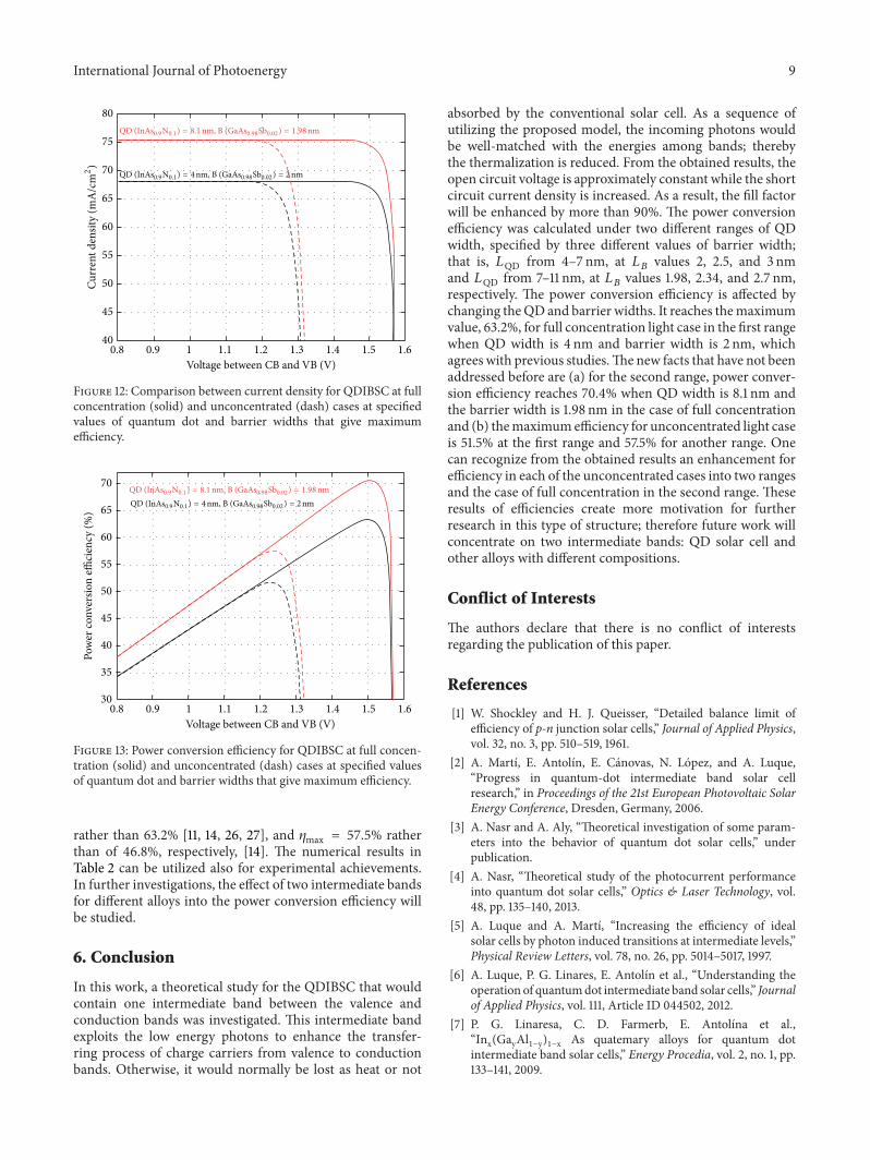
An example of the J-V characteristics for the secondrange of the proposed model is mentioned in Figure 10. Itis important to note that the short circuit current density isrelated to the quantum dot width directly; meanwhile theopen circuit voltage is approximately constant. Additionally,the wide range of the J-V characteristics with short circuitcurrent and open circuit voltage values is confirmed inTable 2. This will contribute to the enhancement of obtainedpower conversion efficiency as shown in Figure 11. One cannotice that the behavior of efficiency is in full agreement withthe obtained results in [25]. But the new contribution is thatthe efficiency in this case, full concentration, reached up to(70.4%) (see also Table 2). The observed enhancement of theefficiency returns to discovering second range. Comparisonbetween J-V characteristics for fully and unconcentratedcases are described in Figure 12. From this figure and Table 2,one can recognize that the second range denotes higher valuesof 𝐽sc and a small amount of increase of 𝑉oc in comparison to

8 International Journal of Photoenergy
0.65
0.6
0.55
8.5 9 9.5 10 10.5 11
QD width at different values of barrier width (nm)
Barrier width:1.98 (nm)2.34 (nm)2.7 (nm)
Ener
gy g
ap b
etw
een
VB
and
IB (e
V)
(a)
8.5 9 9.5 10 10.5 11
1.05
1
0.95
0.9
QD width at different values of barrier width (nm)
Barrier width:1.98 (nm)2.34 (nm)2.7 (nm)
Ener
gy g
ap b
etw
een
IB an
d CB
(eV
)
(b)
Figure 9: (a) Change energy gap between VB and IB according to change in QD width for the second allowable range at different values ofbarrier width. (b) Change energy gap between IB and CB with the same conditions in (a).
80
75
70
65
60
551.25 1.3 1.35 1.4 1.45 1.5 1.55 1.6
Voltage between CB and VB (V)
QD (InAs0.9N0.1) =
B (GaAs0.98Sb0.02) = 1.98nm
8.1nm8.6nm9.1nm
Curr
ent d
ensit
y ∗ge
omet
ric fa
ctor
(mA
/cm
2)
Figure 10: Current density for QDIBSC at full concentration withvarying the quantum dot width and barrier width held constant.
the first range. But in the two considered ranges, the valuesof 𝑉oc in the full concentration case are higher than that inthe unconcentrated case. From a solar cell point of view, thisbehavior normally happens because the allowable large widthof quantum dots will acquire high photons and it then excitesa large number of electrons: high induced current density. Forthe same cases considered before, the comparison betweenthe power conversion efficiency is depicted in Figure 13. Also,the corresponding power conversion efficiency, 𝜂, 𝐽max, 𝑉max,𝐽sc,𝑉oc, and fill factor, 𝐹𝐹, for each combination of QD width(𝐿QD) and barrier width (𝐿
𝐵) for fully and unconcentration
are considered in Table 2. The fill factor pointed in the table
Voltage between CB and VB (V)
75
70
65
60
551.25 1.3 1.35 1.4 1.45 1.5 1.55 1.6
Pow
er co
nver
sion
effici
ency
(%)
QD (InAs0.9N0.1) =
B (GaAs0.98Sb0.02) = 1.98nm
8.1nm8.6nm9.1nm
Figure 11: Power conversion efficiency for QDIBSC at full concen-tration with varying the quantum dot width and barrier width heldconstant.
is determined from (13). It also indicates an enhancementof power conversion efficiency, where 𝐹𝐹 is greater than93% and 90% in the considered cases, respectively. The maintarget of these demonstrations is to compare the obtainedpower conversion efficiency from the first and second ranges.When a full concentration case is taken in the theoreti-cal calculation, higher values of each of the open circuitvoltage and short circuit current density are obtained thatcorrespondingly gave higher power conversion efficiency.When one held comparison between our obtained results andothers in the fully and unconcentrated cases: 𝜂max = 70.4%
International Journal of Photoenergy 9
80
75
70
65
60
55
50
45
400.8 0.9 1 1.1 1.2 1.3 1.4 1.5 1.6
Curr
ent d
ensit
y (m
A/c
m2)
Voltage between CB and VB (V)
QD (InAs0.9N0.1) = 8.1nm, B (GaAs0.98Sb0.02) = 1.98nm
QD (InAs0.9N0.1) = 4nm, B (GaAs0.98Sb0.02) = 2nm
Figure 12: Comparison between current density for QDIBSC at fullconcentration (solid) and unconcentrated (dash) cases at specifiedvalues of quantum dot and barrier widths that give maximumefficiency.
70
65
60
55
50
45
40
35
300.8 0.9 1 1.1 1.2 1.3 1.4 1.5 1.6
Voltage between CB and VB (V)
Pow
er co
nver
sion
effici
ency
(%)
QD (InAs0.9N0.1) = 8.1nm, B (GaAs0.98Sb0.02) = 1.98nmQD (InAs0.9N0.1) = 4nm, B (GaAs0.98Sb0.02) = 2nm
Figure 13: Power conversion efficiency for QDIBSC at full concen-tration (solid) and unconcentrated (dash) cases at specified valuesof quantum dot and barrier widths that give maximum efficiency.
rather than 63.2% [11, 14, 26, 27], and 𝜂max = 57.5% ratherthan of 46.8%, respectively, [14]. The numerical results inTable 2 can be utilized also for experimental achievements.In further investigations, the effect of two intermediate bandsfor different alloys into the power conversion efficiency willbe studied.
6. Conclusion
In this work, a theoretical study for the QDIBSC that wouldcontain one intermediate band between the valence andconduction bands was investigated. This intermediate bandexploits the low energy photons to enhance the transfer-ring process of charge carriers from valence to conductionbands. Otherwise, it would normally be lost as heat or not
absorbed by the conventional solar cell. As a sequence ofutilizing the proposed model, the incoming photons wouldbe well-matched with the energies among bands; therebythe thermalization is reduced. From the obtained results, theopen circuit voltage is approximately constant while the shortcircuit current density is increased. As a result, the fill factorwill be enhanced by more than 90%. The power conversionefficiency was calculated under two different ranges of QDwidth, specified by three different values of barrier width;that is, 𝐿QD from 4–7 nm, at 𝐿
𝐵values 2, 2.5, and 3 nm
and 𝐿QD from 7–11 nm, at 𝐿𝐵values 1.98, 2.34, and 2.7 nm,
respectively. The power conversion efficiency is affected bychanging theQD and barrier widths. It reaches themaximumvalue, 63.2%, for full concentration light case in the first rangewhen QD width is 4 nm and barrier width is 2 nm, whichagrees with previous studies.The new facts that have not beenaddressed before are (a) for the second range, power conver-sion efficiency reaches 70.4% when QD width is 8.1 nm andthe barrier width is 1.98 nm in the case of full concentrationand (b) themaximumefficiency for unconcentrated light caseis 51.5% at the first range and 57.5% for another range. Onecan recognize from the obtained results an enhancement forefficiency in each of the unconcentrated cases into two rangesand the case of full concentration in the second range. Theseresults of efficiencies create more motivation for furtherresearch in this type of structure; therefore future work willconcentrate on two intermediate bands: QD solar cell andother alloys with different compositions.
Conflict of Interests
The authors declare that there is no conflict of interestsregarding the publication of this paper.
References
[1] W. Shockley and H. J. Queisser, “Detailed balance limit ofefficiency of p-n junction solar cells,” Journal of Applied Physics,vol. 32, no. 3, pp. 510–519, 1961.
[2] A. Martı, E. Antolın, E. Canovas, N. Lopez, and A. Luque,“Progress in quantum-dot intermediate band solar cellresearch,” in Proceedings of the 21st European Photovoltaic SolarEnergy Conference, Dresden, Germany, 2006.
[3] A. Nasr and A. Aly, “Theoretical investigation of some param-eters into the behavior of quantum dot solar cells,” underpublication.
[4] A. Nasr, “Theoretical study of the photocurrent performanceinto quantum dot solar cells,” Optics & Laser Technology, vol.48, pp. 135–140, 2013.
[5] A. Luque and A. Martı, “Increasing the efficiency of idealsolar cells by photon induced transitions at intermediate levels,”Physical Review Letters, vol. 78, no. 26, pp. 5014–5017, 1997.
[6] A. Luque, P. G. Linares, E. Antolın et al., “Understanding theoperation of quantumdot intermediate band solar cells,” Journalof Applied Physics, vol. 111, Article ID 044502, 2012.
[7] P. G. Linaresa, C. D. Farmerb, E. Antolına et al.,“Inx(GayAl1−y)1−x As quatemary alloys for quantum dotintermediate band solar cells,” Energy Procedia, vol. 2, no. 1, pp.133–141, 2009.

10 International Journal of Photoenergy
[8] C. - Lin, W.-L. Liu, and C.-Y. Shih, “Detailed balance modelfor intermediate band solar cells with photon conservation,” inProceedings of the 37th IEEE Photovoltaic Specialists Conference(PVSC ’11), 2011.
[9] L. Cuadra, A. Martı, and A. Luque, “Present status of interme-diate band solar cell research,”Thin Solid Films, vol. 451-452, pp.593–599, 2004.
[10] M. Y. Levy, C.Honsberg, A.Marti, andA. Luque, “Quantumdotintermediate band solar cell material systems with negligablevalence band offsets,” inProceedings of the 31st IEEEPhotovoltaicSpecialists Conference, pp. 90–93, January 2005.
[11] Q. Deng, X. Wang, C. Yang et al., “Theoretical study onInxGa1−xN/GaN quantum dots solar cell,” Physica B: CondensedMatter, vol. 406, no. 1, pp. 73–76, 2011.
[12] O. L. Lazarenkova and A. A. Balandin, “Miniband formation ina quantum dot crystal,” Journal of Applied Physics, vol. 89, no.10, pp. 5509–5515, 2001.
[13] Q. Shao, A. A. Balandin, A. I. Fedoseyev, and M. Turowski,“Intermediate-band solar cells based on quantum dot supra-crystals,” Applied Physics Letters, vol. 91, no. 16, Article ID163503, 2007.
[14] E. J. Steven, Quantum dot intermediate band solar cells: designcriteria and optimal materials [Ph.D. thesis], Drexel University,Philadelphia, Pa, USA, 2012.
[15] T. Soga, Nanostructured Materials for Solar Energy Conversion,1st edition, 2006.
[16] S. Birner, Modeling of Semiconductor Nanostructures andSemiconductor-Electrolyte Interfaces, 2011.
[17] S. P. Day, H. Zhou, and D. L. Pulfrey, “The Kronig-Penneyapproximation: may it live on,” IEEE Transactions on Education,vol. 33, no. 4, pp. 355–358, 1990.
[18] R. Aguinaldo, Modeling solutions and simulations for advancedIII-V photovoltaics based on nanostructures [M.S. thesis inmaterials science & engineering], College of Science, RochesterInstitute of Technology, Rochester, NY, USA, 2008.
[19] W. van Roosbroeck andW. Shockley, “Photon-radiative recom-bination of electrons and holes in germanium,” Physical Review,vol. 94, no. 6, pp. 1558–1560, 1954.
[20] A. Martı, L. Cuadra, and A. Luque, “Quasi-drift diffusionmodel for the quantum dot intermediate band solar cell,” IEEETransactions on Electron Devices, vol. 49, no. 9, pp. 1632–1639,2002.
[21] L. A. Kosyachenko, Solar Cells—New Aspects and Solutions,2011.
[22] S. P. Bremner and C. B. Honsberg, “Intermediate band solarcell with non-ideal band structure under AMl.5 spectrum,” inProceedings of the 38th IEEE Photovoltaic Specialists Conference(PVSC ’12), 2012.
[23] A. Martı, L. Cuadra, and A. Luque, “Partial filling of a quantumdot intermediate band for solar cells,” IEEE Transactions onElectron Devices, vol. 48, no. 10, pp. 2394–2399, 2001.
[24] J. Ojajarvi, Tetrahedral chalcopyrite quantum dots in solar-cellapplications [M.S. thesis], Department of Physics, University ofJyvaskyla, 2010.
[25] A. Luque, A. Martı, and L. Cuadra, “Impact-ionization-assistedintermediate band solar cell,” IEEE Transactions on ElectronDevices, vol. 50, no. 2, pp. 447–454, 2003.
[26] Q.-W. Deng, X.-L. Wang, C.-B. Yang et al., “Computationalinvestigation of InxGa1−xN/InN quantum-dot intermediate-band solar cell,” Chinese Physics Letters, vol. 28, no. 1, ArticleID 018401, 2011.
[27] A. Nasr, “Theoretical model for observation of the conversionefficiency into quantumdot solar cells,” under publication.

Submit your manuscripts athttp://www.hindawi.com
Hindawi Publishing Corporationhttp://www.hindawi.com Volume 2014
Inorganic ChemistryInternational Journal of
Hindawi Publishing Corporation http://www.hindawi.com Volume 2014
International Journal ofPhotoenergy
Hindawi Publishing Corporationhttp://www.hindawi.com Volume 2014
Carbohydrate Chemistry
International Journal of
Hindawi Publishing Corporationhttp://www.hindawi.com Volume 2014
Journal of
Chemistry
Hindawi Publishing Corporationhttp://www.hindawi.com Volume 2014
Advances in
Physical Chemistry
Hindawi Publishing Corporationhttp://www.hindawi.com
Analytical Methods in Chemistry
Journal of
Volume 2014
Bioinorganic Chemistry and ApplicationsHindawi Publishing Corporationhttp://www.hindawi.com Volume 2014
SpectroscopyInternational Journal of
Hindawi Publishing Corporationhttp://www.hindawi.com Volume 2014
The Scientific World JournalHindawi Publishing Corporation http://www.hindawi.com Volume 2014
Medicinal ChemistryInternational Journal of
Hindawi Publishing Corporationhttp://www.hindawi.com Volume 2014
Chromatography Research International
Hindawi Publishing Corporationhttp://www.hindawi.com Volume 2014
Applied ChemistryJournal of
Hindawi Publishing Corporationhttp://www.hindawi.com Volume 2014
Hindawi Publishing Corporationhttp://www.hindawi.com Volume 2014
Theoretical ChemistryJournal of
Hindawi Publishing Corporationhttp://www.hindawi.com Volume 2014
Journal of
Spectroscopy
Analytical ChemistryInternational Journal of
Hindawi Publishing Corporationhttp://www.hindawi.com Volume 2014
Journal of
Hindawi Publishing Corporationhttp://www.hindawi.com Volume 2014
Quantum Chemistry
Hindawi Publishing Corporationhttp://www.hindawi.com Volume 2014
Organic Chemistry International
ElectrochemistryInternational Journal of
Hindawi Publishing Corporation http://www.hindawi.com Volume 2014
Hindawi Publishing Corporationhttp://www.hindawi.com Volume 2014
CatalystsJournal of


