
Reporter : Hsun-Pei Wu Advisor : Cheng-Hsin Chuang Department of Mechanical Engineering & Institute...
15
Reporter : Hsun-Pei Wu Advisor : Cheng-Hsin Chuang Department of Mechanical Engineering & Institute of Nanotechnology, Southern Taiwan University, Tainan, TAIWAN March 28th Enhancement of Fluorescent Intensity by Using DEP Manipulations of Polyaniline-coated Al 2 O 3 Nanoparticles for Immunosensing
-
Upload
briana-stevens -
Category
Documents
-
view
230 -
download
4
Transcript of Reporter : Hsun-Pei Wu Advisor : Cheng-Hsin Chuang Department of Mechanical Engineering & Institute...
Reporter : Hsun-Pei Wu
Advisor : Cheng-Hsin Chuang
Department of Mechanical Engineering & Institute of Nanotechnology,
Southern Taiwan University, Tainan, TAIWANMarch 28th
Enhancement of Fluorescent Intensity by Using DEP Manipulations of Polyaniline-coated Al2O3
Nanoparticles for Immunosensing
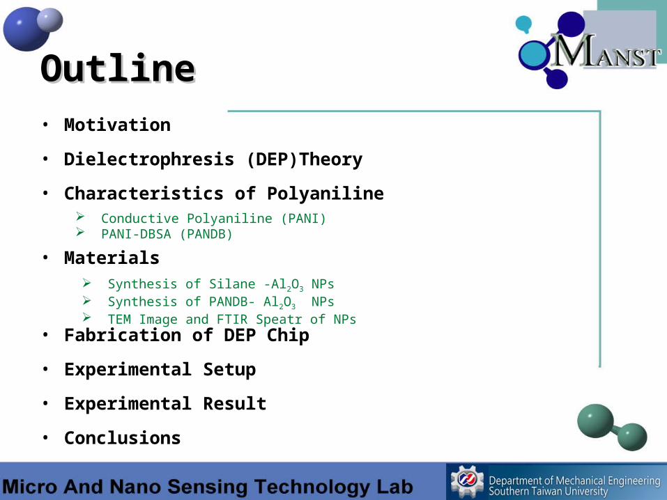
OutlineOutline• Motivation
• Dielectrophresis (DEP)Theory
• Characteristics of Polyaniline
• Materials
• Fabrication of DEP Chip
• Experimental Setup
• Experimental Result
• Conclusions
Conductive Polyaniline (PANI) PANI-DBSA (PANDB)
Synthesis of Silane -Al2O3 NPs Synthesis of PANDB- Al2O3 NPs TEM Image and FTIR Speatr of NPs
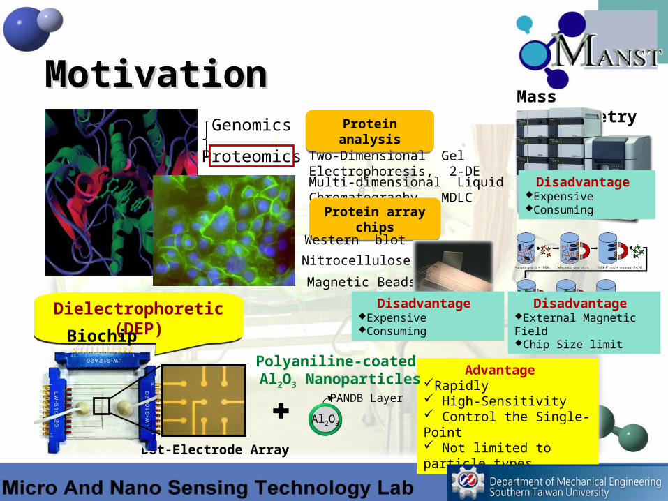
MotivationMotivation
Dot-Electrode Array
Genomics
Proteomics
Protein analysisProtein analysis
Two-Dimensional Gel Electrophoresis, 2-DE
Multi-dimensional Liquid Chromatography, MDLC
Mass Spectrometry
Disadvantage ExpensiveConsumingProtein array chipsProtein array chips
Western blot
Nitrocellulose
Magnetic Beads
Disadvantage External Magnetic FieldChip Size limit
Dielectrophoretic (DEP)Dielectrophoretic (DEP)
Biochip
Disadvantage ExpensiveConsuming
Advantage Rapidly High-Sensitivity Control the Single-Point Not limited to particle types
Polyaniline-coated Al2O3 Nanoparticles
PANDB Layer
Al2O3
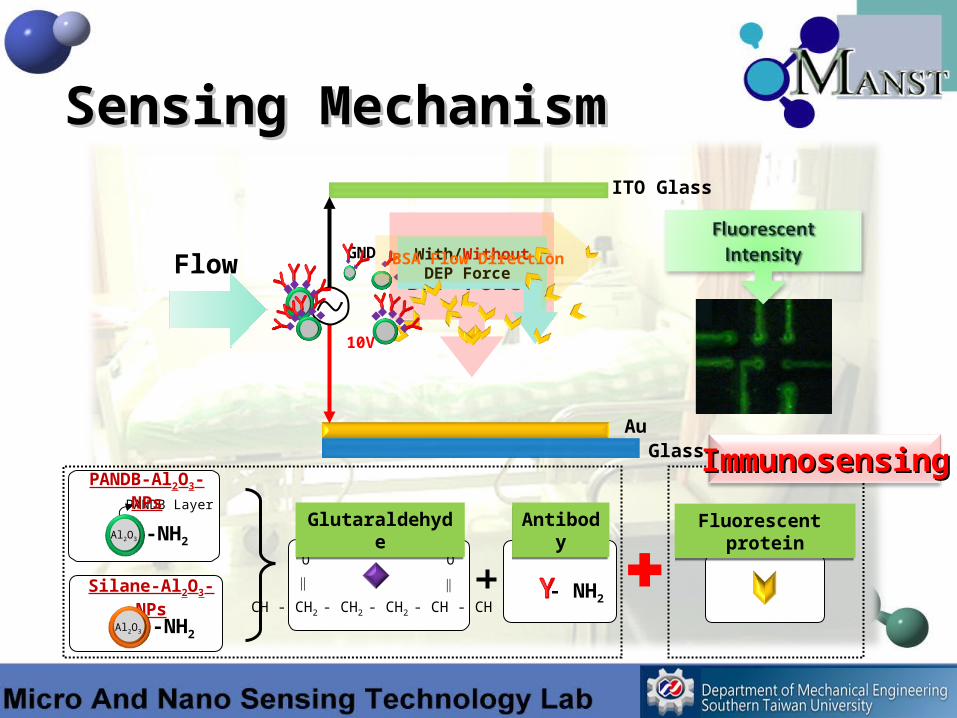
Positive DEP Force
GND
10V
ITO Glass
GlassAu
With/Without DEP Force
BSA Flow DirectionFlow
O
∥
O
∥
CH - CH2 - CH2 - CH2 - CH - CH - NH2
PANDB Layer
-NH2
PANDB-Al2O3-NPs
Al2O3
Silane-Al2O3-NPs
-NH2
GlutaraldehydeGlutaraldehyde AntibodyAntibody
Al2O3
Fluorescent proteinFluorescent protein
Sensing MechanismSensing Mechanism
ImmunosensingImmunosensing
5
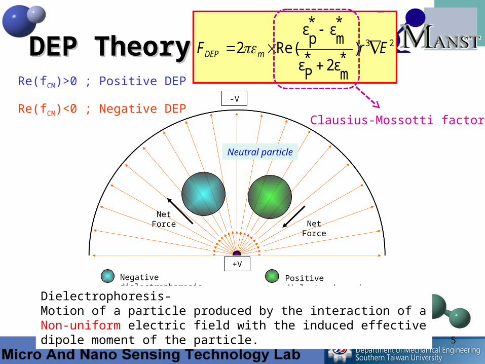
Negative dielectrophoresis Positive dielectrophoresis
+V
-V
Neutral particle
Net ForceNet Force
DEPDEP TheoryTheory
Dielectrophoresis- Motion of a particle produced by the interaction of a Non-uniform electric field with the induced effective dipole moment of the particle.
23)*m
2ε*P
ε
*m
ε*p
εRe(2 ErF mDEP
Clausius-Mossotti factor
Re(fCM)>0 ; Positive DEP
Re(fCM)<0 ; Negative DEP
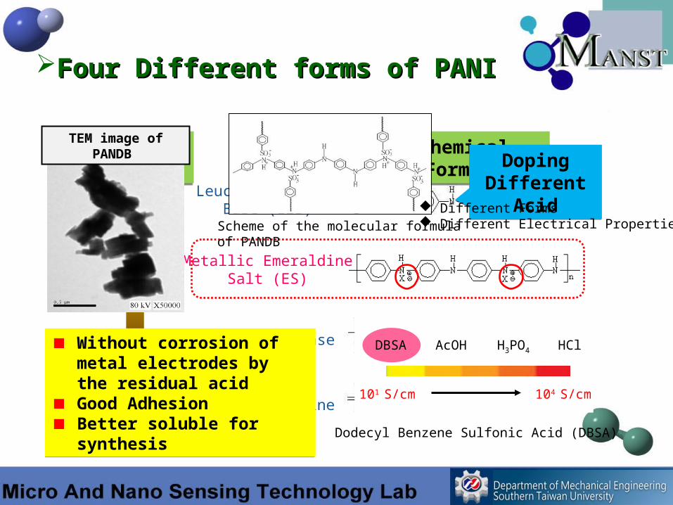
Four Different forms of PANIFour Different forms of PANI
Reduced State
Oxidized State
Redox StateRedox State FormsForms
Pernigraniline Base(PNB)
Metallic Emeraldine Salt (ES)
Emeraldine Base (EB)
Leuco emeraldine Base (LEB)
Chemical FormulaChemical Formula
Dodecyl Benzene Sulfonic Acid (DBSA)
HClAcOH H3PO4DBSA
104 S/cm101 S/cm
Doping Different Acid
Doping Different Acid
Without corrosion of metal electrodes by the residual acidGood AdhesionBetter soluble for synthesis
Without corrosion of metal electrodes by the residual acidGood AdhesionBetter soluble for synthesis
Scheme of the molecular formula of PANDB
TEM image of PANDB
Different Forms Different Electrical Properties
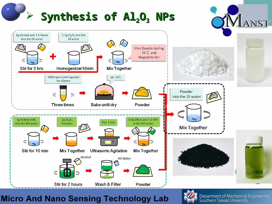
Synthesis of AlSynthesis of Al22OO33 NPs NPs
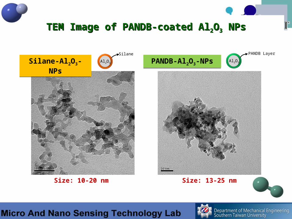
TEM Image of PANDB-coated AlTEM Image of PANDB-coated Al22OO33 NPs NPs
Silane-Al2O3-NPsSilane-Al2O3-NPs PANDB-Al2O3-NPsPANDB-Al2O3-NPsAl2O3
Silane
Al2O3
PANDB Layer
Size: 10-20 nm Size: 13-25 nm
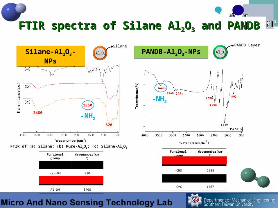
FTIR spectra of Silane AlFTIR spectra of Silane Al22OO33 and PANDB and PANDB
Funtional group Wavenumber(cm-1)
-NH2 3444
-CH3 2958
-CH2- 2920
-C=C 1467
Silane-Al2O3-NPsSilane-Al2O3-NPs PANDB-Al2O3-NPsPANDB-Al2O3-NPsAl2O3
Silane
Al2O3
PANDB Layer
Funtional group Wavenumber(cm-1)
-Si-O-Al 810 、 1076
-Si-OH 920
-NH2 1560
Al-OH 3400
1550
820
3480
(a)
(b)
(c)
FTIR of (a) Silane; (b) Pure-Al2O3; (c) Silane-Al2O3
-NH2
-NH2
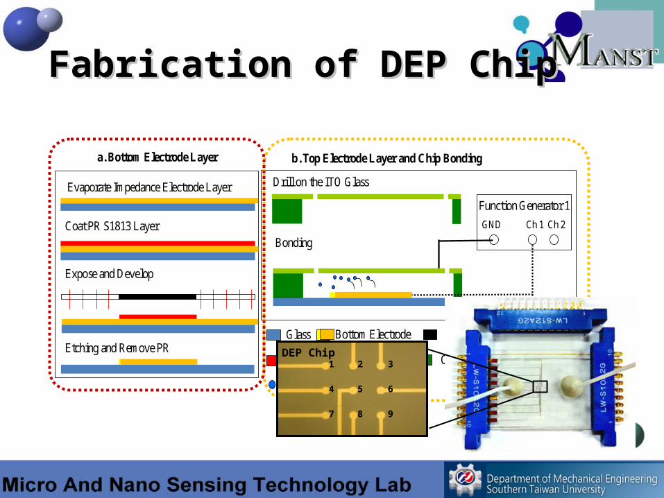
Fabrication of DEP ChipFabrication of DEP Chip
a. Bottom Electrode Layer
Evaporate Impedance Electrode Layer
Coat PR S1813 Layer
Expose and Develop
Etching and Remove PR
b. Top Electrode Layer and Chip Bonding
Drill on the ITO Glass
Bonding
Function Generator 1
Ch 1 Ch 2GND
Ch 1: DEP Trap Nano-particle
Optical Clean Adhesive(OCA) PR S1813
Photomask
Nano-particle
Glass Bottom Electrode
ITO Glass
5 6
7 8 9
4
1 2 3DEP Chip

Experimental Setup Experimental Setup
GND
5 6
7 8 9
4
1 2 3DEP Chip
OutletInlet
Function Generator
Voltage: 10 VppFrequency: 10~50 kHz
0 10 20 30
Im m unosensing Tim e (m in)
0.8
1.2
1.6
2
2.4
No
rmal
ized
Flu
ore
scen
t In
ten
sity
( I
t /
I t =
0 )
F luorescent In tensity For Differen t Vo ltage 0 Vpp
2 Vpp
4 Vpp
6 Vpp
8 Vpp
10 Vpp
CCD Camera Fluorescent Image
Fluorescent Intensity
Syringe Pumps
LabVIEW Program
5 6
7 8 9
10
1 2 3
4
Circuit Board DAQ System
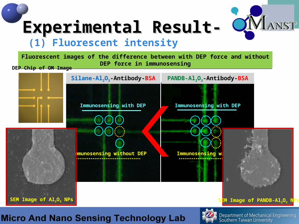
Experimental Result-Experimental Result- (1) Fluorescent intensity
Fluorescent images of the difference between with DEP force and without DEP force in immunosensing
Fluorescent images of the difference between with DEP force and without DEP force in immunosensing
Silane-Al2O3-Antibody-BSA PANDB-Al2O3-Antibody-BSA
Immunosensing with DEP
Immunosensing without DEP
Immunosensing with DEP
Immunosensing without DEP
DEP Chip of OM Image
SEM Image of Al2O3 NPs SEM Image of PANDB-Al2O3 NPs
With DEP
Without DEP
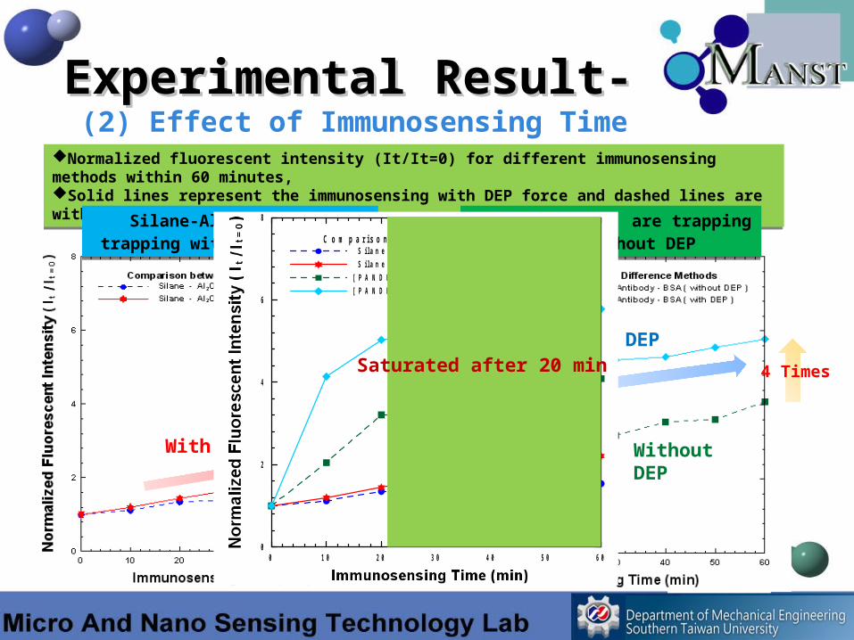
Normalized fluorescent intensity (It/It=0) for different immunosensing methods within 60 minutes, Solid lines represent the immunosensing with DEP force and dashed lines are without DEP as immunosensing
Normalized fluorescent intensity (It/It=0) for different immunosensing methods within 60 minutes, Solid lines represent the immunosensing with DEP force and dashed lines are without DEP as immunosensing
Silane-Al2O3-NPs are trapping with /without DEP
Silane-Al2O3-NPs are trapping with /without DEP
PANDB-Al2O3-NPs are trapping with /without DEP
PANDB-Al2O3-NPs are trapping with /without DEP
1 Times
Without DEP
With DEP
4 Times
0 10 20 30 40 50 60
Im m unosensing Tim e (m in)
0
2
4
6
8
No
rmal
ize
d F
luo
res
cen
t In
ten
sity
( I
t /
I t =
0 )
Comparison between Difference Methods Silane - Al2O 3 - Antibody - BSA ( without DEP )
Silane - Al2O 3 - Antibody - BSA ( with DEP )
[ PANDB-Al2O 3 ] - Antibody - BSA ( without DEP )
[ PANDB-Al2O 3 ] - Antibody - BSA ( with DEP )
Saturated after 20 min
Experimental Result-Experimental Result- (2) Effect of Immunosensing Time
ConclusionsConclusions We developed a DEP chip with a dot-electrode array for the condensation
of NPs and the enhancement of fluorescent intensity under a programmable control system.
According to the experimental results of fluorescent intensities, the intensity increased with either of applied time and immunosensing with p-DEP force.
This technology could apply to the biosensor such as immunoassay when the immobilized NPs as specific biomarkers.
In the future, our biosensor can integrate with PANDB material and impedance detection on to the immunoassay.