
REPORT DOCUMENTATION PAGE Form ApprovedABSTRACT Infrared Spectroscopic Measurement of Titanium...
166
Standard Form 298 (Rev 8/98) Prescribed by ANSI Std. Z39.18 540-231-2472 W911NF-09-1-0150 55374-CH.22 MS Thesis a. REPORT 14. ABSTRACT 16. SECURITY CLASSIFICATION OF: Within the ‘forbidden’ range of electron energies between the valence and conduction bands of titanium dioxide, crystal lattice irregularities lead to the formation of electron trapping sites. These sites are known as shallow trap states, where ‘shallow’ refers to the close energy proximity of those features to the bottom of the semiconductor conduction band. For wide bandgap semiconductors like titanium dioxide, shallow electron traps are the principle route for thermal excitation of electrons into the conduction band. The studies described here employ a novel infrared spectroscopic approach to determine the energy of shallow 1. REPORT DATE (DD-MM-YYYY) 4. TITLE AND SUBTITLE 13. SUPPLEMENTARY NOTES 12. DISTRIBUTION AVAILIBILITY STATEMENT 6. AUTHORS 7. PERFORMING ORGANIZATION NAMES AND ADDRESSES 15. SUBJECT TERMS b. ABSTRACT 2. REPORT TYPE 17. LIMITATION OF ABSTRACT 15. NUMBER OF PAGES 5d. PROJECT NUMBER 5e. TASK NUMBER 5f. WORK UNIT NUMBER 5c. PROGRAM ELEMENT NUMBER 5b. GRANT NUMBER 5a. CONTRACT NUMBER Form Approved OMB NO. 0704-0188 3. DATES COVERED (From - To) - UU UU UU UU 14-07-2015 Approved for public release; distribution is unlimited. Infrared Spectroscopic Measurement of Titanium Dioxide Nanoparticle Shallow Trap State Energies The views, opinions and/or findings contained in this report are those of the author(s) and should not contrued as an official Department of the Army position, policy or decision, unless so designated by other documentation. 9. SPONSORING/MONITORING AGENCY NAME(S) AND ADDRESS (ES) U.S. Army Research Office P.O. Box 12211 Research Triangle Park, NC 27709-2211 FTIR, TiO2, Nanoparticle, Trapped Electrons REPORT DOCUMENTATION PAGE 11. SPONSOR/MONITOR'S REPORT NUMBER(S) 10. SPONSOR/MONITOR'S ACRONYM(S) ARO 8. PERFORMING ORGANIZATION REPORT NUMBER 19a. NAME OF RESPONSIBLE PERSON 19b. TELEPHONE NUMBER John Morris Steven P. Burrows 611102 c. THIS PAGE The public reporting burden for this collection of information is estimated to average 1 hour per response, including the time for reviewing instructions, searching existing data sources, gathering and maintaining the data needed, and completing and reviewing the collection of information. Send comments regarding this burden estimate or any other aspect of this collection of information, including suggesstions for reducing this burden, to Washington Headquarters Services, Directorate for Information Operations and Reports, 1215 Jefferson Davis Highway, Suite 1204, Arlington VA, 22202-4302. Respondents should be aware that notwithstanding any other provision of law, no person shall be subject to any oenalty for failing to comply with a collection of information if it does not display a currently valid OMB control number. PLEASE DO NOT RETURN YOUR FORM TO THE ABOVE ADDRESS. Virginia Polytechnic Institute & State Unive North End Center, Suite 4200 300 Turner Street, NW Blacksburg, VA 24061 -0001
Transcript of REPORT DOCUMENTATION PAGE Form ApprovedABSTRACT Infrared Spectroscopic Measurement of Titanium...

Standard Form 298 (Rev 8/98) Prescribed by ANSI Std. Z39.18
540-231-2472
W911NF-09-1-0150
55374-CH.22
MS Thesis
a. REPORT
14. ABSTRACT
16. SECURITY CLASSIFICATION OF:
Within the ‘forbidden’ range of electron energies between the valence and conduction bands of titanium dioxide, crystal lattice irregularities lead to the formation of electron trapping sites. These sites are known as shallow trap states, where ‘shallow’ refers to the close energy proximity of those features to the bottom of the semiconductor conduction band. For wide bandgap semiconductors like titanium dioxide, shallow electron traps are the principle route for thermal excitation of electrons into the conduction band.The studies described here employ a novel infrared spectroscopic approach to determine the energy of shallow
1. REPORT DATE (DD-MM-YYYY)
4. TITLE AND SUBTITLE
13. SUPPLEMENTARY NOTES
12. DISTRIBUTION AVAILIBILITY STATEMENT
6. AUTHORS
7. PERFORMING ORGANIZATION NAMES AND ADDRESSES
15. SUBJECT TERMS
b. ABSTRACT
2. REPORT TYPE
17. LIMITATION OF ABSTRACT
15. NUMBER OF PAGES
5d. PROJECT NUMBER
5e. TASK NUMBER
5f. WORK UNIT NUMBER
5c. PROGRAM ELEMENT NUMBER
5b. GRANT NUMBER
5a. CONTRACT NUMBER
Form Approved OMB NO. 0704-0188
3. DATES COVERED (From - To)-
UU UU UU UU
14-07-2015
Approved for public release; distribution is unlimited.
Infrared Spectroscopic Measurement of Titanium Dioxide Nanoparticle Shallow Trap State Energies
The views, opinions and/or findings contained in this report are those of the author(s) and should not contrued as an official Department of the Army position, policy or decision, unless so designated by other documentation.
9. SPONSORING/MONITORING AGENCY NAME(S) AND ADDRESS(ES)
U.S. Army Research Office P.O. Box 12211 Research Triangle Park, NC 27709-2211
FTIR, TiO2, Nanoparticle, Trapped Electrons
REPORT DOCUMENTATION PAGE
11. SPONSOR/MONITOR'S REPORT NUMBER(S)
10. SPONSOR/MONITOR'S ACRONYM(S) ARO
8. PERFORMING ORGANIZATION REPORT NUMBER
19a. NAME OF RESPONSIBLE PERSON
19b. TELEPHONE NUMBERJohn Morris
Steven P. Burrows
611102
c. THIS PAGE
The public reporting burden for this collection of information is estimated to average 1 hour per response, including the time for reviewing instructions, searching existing data sources, gathering and maintaining the data needed, and completing and reviewing the collection of information. Send comments regarding this burden estimate or any other aspect of this collection of information, including suggesstions for reducing this burden, to Washington Headquarters Services, Directorate for Information Operations and Reports, 1215 Jefferson Davis Highway, Suite 1204, Arlington VA, 22202-4302. Respondents should be aware that notwithstanding any other provision of law, no person shall be subject to any oenalty for failing to comply with a collection of information if it does not display a currently valid OMB control number.PLEASE DO NOT RETURN YOUR FORM TO THE ABOVE ADDRESS.
Virginia Polytechnic Institute & State UniversityNorth End Center, Suite 4200300 Turner Street, NWBlacksburg, VA 24061 -0001

ABSTRACT
Infrared Spectroscopic Measurement of Titanium Dioxide Nanoparticle Shallow Trap State Energies
Report Title
Within the ‘forbidden’ range of electron energies between the valence and conduction bands of titanium dioxide, crystal lattice irregularities lead to the formation of electron trapping sites. These sites are known as shallow trap states, where ‘shallow’ refers to the close energy proximity of those features to the bottom of the semiconductor conduction band. For wide bandgap semiconductors like titanium dioxide, shallow electron traps are the principle route for thermal excitation of electrons into the conduction band.The studies described here employ a novel infrared spectroscopic approach to determine the energy of shallow electron traps in titanium dioxide nanoparticles. Mobile electrons within the conduction band of semiconductors are known to absorb infrared radiation. As those electrons absorb the infrared photons, transitions within the continuum of the conduction band produce a broad spectral signal across the entire mid-infrared range. A Mathematical expression based upon Fermi – Dirac statistics was derived to correlate the temperature of the particles to the population of charge carriers, as measured through the infrared absorbance. The primary variable of interest in the Fermi – Dirac expression is the energy difference between the shallow trap states and the conduction band. Fitting data sets consisting of titanium dioxide nanoparticle temperatures and their associated infrared spectra, over a defined frequency range, to the Fermi – Dirac expression is used to determine the shallow electron trap state energy.

Infrared Spectroscopic Measurement of Titanium Dioxide
Nanoparticle Shallow Trap State Energies
Steven P. Burrows
Thesis submitted to the faculty of the Virginia Polytechnic Institute and State University in partial fulfillment of the requirements for the degree of
MASTER OF SCIENCE
in Chemistry
John R. Morris, Chair
Karen J. Brewer Gary L. Long
February 10, 2010
Blacksburg, Virginia
Keywords: nanoparticles, semiconductor, titanium dioxide, conduction band electrons, catalysis, infrared spectroscopy, shallow trap state

Infrared Spectroscopic Measurement of Titanium Dioxide Nanoparticle Shallow Trap State Energies
Steven P. Burrows
ABSTRACT
Within the ‘forbidden’ range of electron energies between the valence and conduction
bands of titanium dioxide, crystal lattice irregularities lead to the formation of electron trapping
sites. These sites are known as shallow trap states, where ‘shallow’ refers to the close energy
proximity of those features to the bottom of the semiconductor conduction band. For wide
bandgap semiconductors like titanium dioxide, shallow electron traps are the principle route for
thermal excitation of electrons into the conduction band.
The studies described here employ a novel infrared spectroscopic approach to determine
the energy of shallow electron traps in titanium dioxide nanoparticles. Mobile electrons within
the conduction band of semiconductors are known to absorb infrared radiation. As those
electrons absorb the infrared photons, transitions within the continuum of the conduction band
produce a broad spectral signal across the entire mid-infrared range. A Mathematical expression
based upon Fermi – Dirac statistics was derived to correlate the temperature of the particles to
the population of charge carriers, as measured through the infrared absorbance. The primary
variable of interest in the Fermi – Dirac expression is the energy difference between the shallow
trap states and the conduction band. Fitting data sets consisting of titanium dioxide nanoparticle
temperatures and their associated infrared spectra, over a defined frequency range, to the Fermi –
Dirac expression is used to determine the shallow electron trap state energy.

iii
ACKNOWLEDGEMENTS
I would like to thank my advisor, Dr. John R. Morris for the opportunity to participate in
this work, within his research group. I hope that we can continue this work as part of my pursuit
of a Ph. D. at Virginia Tech.
There are many persons within the Chemistry faculty that have assisted, advised, and
encouraged me over the years, both during my work on this degree and in the years preceding
my start as a graduate student. I would like to thank Professor Brian Tissue for allowing me the
use of his laser vaporization apparatus and the training for its correct operation. I also would like
to extend thanks to Professor Gary L. Long and Professor Karen Brewer for agreeing to be part
of my degree committee.
I would like to thank Ms. Kathy Lowe at the Morphology Lab of the Virginia – Maryland
Regional College of Veterinary Medicine for her enormous help with obtaining transmission
electron microscopy images of my nanoparticle preparations. Similar recognition is in order for
Mr. John McIntosh of the Institute for Critical Technology and Applied Science for his
assistance with high resolution transmission electron microscopy and electron diffraction
characterization. I would also like to thank Dr. Carla Slebodnick of the Virginia Tech
Crystallography Lab for her help with obtaining powder x-ray diffraction patterns of my
nanoparticle preparations.
I would like to also thank past and present members of the Morris Group for many useful
discussions and advice that has helped me navigate some of the more subtle and undocumented
intricacies of graduate school. Particularly, I would like to thank Dr. Dimitar Panayotov (a.k.a.
Mitko) for much patience and instruction in nanoparticle catalysis, and for the use of his
apparatus, materials, and data.
Finally, I would like to thank my wife, Becky, for her unwavering support and
encouragement, which have continued since the very beginning of the crazy idea that I should
attempt to go through graduate school as a ‘non-traditional’ (i.e. old) student.

iv
TABLE OF CONTENTS
Chapter 1: Titanium Dioxide Nanoparticles and Electrons in the Solid State .......................1 1.1 Introduction.......................................................................................................................1
1.2 Electrons in the Crystalline Solid State..............................................................................3 1.2.1 Probability Distributions for Particle Energies ............................................................3 1.2.2 Classical Free Electron Models.................................................................................10 1.2.3 Quantized Free Electron Model.................................................................................14 1.2.4 The Band Theory Model ...........................................................................................17 1.2.5 Band Structure Classification of Solid Phase Matter .................................................24
1.3 Titanium Dioxide.............................................................................................................28 1.3.1 General Properties ....................................................................................................28 1.3.2 Semiconductor Doping and Trap States ....................................................................33 1.3.3 The Titanium Dioxide Crystal Surface......................................................................37 1.3.4 Titanium Dioxide Nanoparticles and Shallow Electron Trap States...........................40
1.4 Titanium Dioxide Nanoparticle Preparation....................................................................41 1.4.1 Liquid Preparation Techniques .................................................................................41 1.4.2 Vapor Pyrolysis ........................................................................................................45 1.4.3 Laser Techniques......................................................................................................47
1.5 Infrared Spectroscopy of Electrons..................................................................................50 1.5.1 Evidence for the Infrared Detection of Conduction Band Electrons...........................50 1.5.2 Characteristics of the TiO2 IR Baseline .....................................................................52 1.5.3 Electron Density Measurement from Infrared Absorption .........................................57
Chapter 2: Nanoparticle Preparation, Characterization, and Spectroscopy........................62
2.1 Introduction.....................................................................................................................62 2.2 Nanoparticle Preparation by Laser Vaporization ............................................................62
2.2.1 Description of Apparatus ..........................................................................................62 2.2.2 Nanoparticle Synthesis..............................................................................................66
2.3 Transmission Electron Microscopy..................................................................................68 2.3.1 Image Resolution......................................................................................................68 2.3.2 Electron Microscope Operation Modes .....................................................................70 2.3.3 Nanoparticle Preparation for Electron Microscopy....................................................72
2.4 X-ray Diffraction .............................................................................................................73 2.4.1 The Bragg Condition ................................................................................................73 2.4.2 Production of X-rays.................................................................................................74 2.4.3 Powder Diffraction ...................................................................................................75 2.4.4 Sample Preparation and Diffraction Pattern Collection..............................................76
2.5 Infrared Observation of Electron Transitions ..................................................................77 2.5.1 Fourier Transform IR Spectroscopy ..........................................................................77

v
2.5.2 The Vacuum FTIR Cell ............................................................................................81 2.5.3 Sample Preparation and Conditioning .......................................................................85 2.5.4 Temperature Ramp Infrared Spectra Collection.........................................................88
Chapter 3: Data Analysis........................................................................................................90
3.1 Electron Microscopy Particle Diameter Measurements ...................................................90 3.2 Powder X-ray Diffraction ................................................................................................94
3.3 FTIR Data Processing and Shallow Trap Energy Calculation .........................................98
Chapter 4: Discussion of Results and Conclusions ..............................................................103
4.1 Review of Research Objectives ......................................................................................103 4.2 Nanoparticle Sizes and Size Distributions......................................................................103
4.3 Shallow Trap State Energy Measurements .....................................................................105 4.4 Estimation of Electron Shallow Traps Population..........................................................107
4.5 FTIR Surface Chemistry Observation and Electron Monitoring.....................................110 4.6 Future Work ..................................................................................................................111
Appendix A: Density of States Derivation............................................................................114 Appendix B: Fermi-Dirac Distribution Derivation..............................................................119 Appendix C: FORTRAN Program WaveShave.f ................................................................122 Appendix D: FORTRAN Program Trapint2.f.....................................................................124 Appendix E: Nanoparticle Size Measurement Data Summary ...........................................127 Appendix F: SPB018 Transmission Electron Micrograph ..................................................128 Appendix G: SPB020 Transmission Electron Micrograph .................................................129 Appendix H: SPB018 High Resolution Transmission Electron Micrograph......................130 Appendix I: Conduction Band Electron Population Calculation........................................131
References..............................................................................................................................133

vi
LIST OF FIGURES
Figure 1: Semiconductor band structure and trap states within a nanoparticle. . ..........................3
Figure 2: The Maxwell distribution of nitrogen at T = 298K and T = 1298K. .............................9
Figure 3: The Thomson cathode ray deflection experiment....................................................... 11
Figure 4: Filling of electron states at the Fermi energy (EF). ..................................................... 15
Figure 5: A hypothetical one-dimensional lattice...................................................................... 19
Figure 6: The Kronig – Penny model........................................................................................ 20
Figure 7: Alternating Kronig – Penny model forbidden and allowed electron energy states. ..... 22
Figure 8: Electron band structure for the Kronig – Penny model for a value of P = 2. ............... 23
Figure 9: Classification of solid-phase materials from band structure. ...................................... 25
Figure 10: Semiconductor band structure for the electron energy as a function of the k→→
electron momentum vector. ...................................................................................................... 26
Figure 11: Direct (a) and indirect (b) semiconductor excitations. .............................................. 27
Figure 12: Unit cell structures for rutile and anatase polymorphs of titanium dioxide. .............. 30
Figure 13: Phosphorus n-doping of a germanium semiconductor. ............................................ 33
Figure 14: Boron p-doping of a germanium semiconductor. ..................................................... 34
Figure 15: Titanium dioxide surface trapping of electrons. ....................................................... 35
Figure 16: Surface irregularities on a crystal lattice. ................................................................. 38
Figure 17: Aspects of the rutile TiO2 surface. ........................................................................... 39
Figure 18: Titanium dioxide tube furnace pyrolysis reactor. ..................................................... 46
Figure 19: Flame pyrolysis nanoparticle generation.................................................................. 46
Figure 20: A typical setup for synthesis of nanoparticles with laser heating.............................. 49

vii
Figure 21: Vibrational wave propagation in crystal lattices....................................................... 52
Figure 22: Phonon coupling to free carrier absorbance in titanium dioxide. .............................. 53
Figure 23: Superposition of interfacial WO3 infrared spectrum (a) with TiO2 sample
spectrum (b) to produce composite infrared spectrum (c). ........................................................ 56
Figure 24: Development of conduction band electron density expression. ................................ 58
Figure 25: Schematic of laser evaporation chamber used for
nanoparticle synthesis (end view). ............................................................................................ 63
Figure 26: Vaporization chamber laser optics (top view). ......................................................... 64
Figure 27: Details of hemispherical collector dome placement. ................................................ 66
Figure 28: Electron diffraction in a transmission electron microscope. ..................................... 71
Figure 29: Diagram for electron optics of a transmission electron microscope operated in
(a) magnification, and (b) electron diffraction modes. .............................................................. 72
Figure 30: Bragg refraction from a crystal lattice...................................................................... 74
Figure 31: Electron transitions associated with some x-ray radiation sources............................ 75
Figure 32: Powder x-ray diffraction.......................................................................................... 76
Figure 33: Gemini x-ray diffractometer powder sample tube preparation steps. ........................ 77
Figure 34: The Michelson interferometer. ................................................................................ 79
Figure 35: FTIR high vacuum cell............................................................................................ 82
Figure 36: Vacuum cell installed onto Mattson RS-10000 FTIR spectrometer. ......................... 83
Figure 37: Tungsten mesh nanoparticle stage assembly. ........................................................... 84
Figure 38: Nanoparticle press mold assembly........................................................................... 87
Figure 39: Nanoparticle mean diameter as a function of laser vaporization
chamber O2 pressure. ............................................................................................................... 93
Figure 40: X-ray diffraction pattern for an empty, 0.3 mm sample capillary. ............................ 95
Figure 41: Degussa P25 titanium dioxide nanoparticle XRD pattern with
Sonneveld – Visser baseline correction. ................................................................................... 96

viii
Figure 42: X-ray diffraction nanoparticle characterization. ....................................................... 97
Figure 43: Nonlinear regression curve-fit spreadsheet for the Fermi-Dirac relationship. ..........100
Figure 44: Integrated area vs. temperature plots for 4 nm (circle symbols)
and 30 nm (triangle symbols) TiO2..........................................................................................102
Figure 45: Transmission electron micrographs for SPB014 and SPB015
titanium dioxide nanoparticle batches......................................................................................104
Figure 46: The shallow trap state energy difference of titanium dioxide relative to
the band structure. ...................................................................................................................107
Figure 47: Nanoparticle FTIR flow cell. ..................................................................................112
Figure 48: k→→
vector space for an electron. ...............................................................................115
Figure 49: Acceptable wave function positions in the x-y plane...............................................116
Figure 50: TEM micrograph for SPB018 4.0 ± 0.6 nm titanium dioxide nanoparticles.............128
Figure 51: TEM micrograph for SPB020 30 ± 10 nm titanium dioxide nanoparticles. .............129
Figure 52: High resolution micrograph of SPB018 titanium dioxide nanoparticles. .................130

ix
LIST OF EQUATIONS
(1) Maxwell’s distribution..........................................................................................................5
(2) Maxwell’s distribution (rearranged, with Boltzmann constant) .............................................6
(3) Maxwell’s distribution (probability distribution) ..................................................................6
(4) Maxwell’s distribution (probability function form) ...............................................................6
(5) Mean speed...........................................................................................................................7
(6) Root mean speed...................................................................................................................7
(7) Most probable speed .............................................................................................................7
(8) Relative mean speed (equal mass particles)...........................................................................7
(9) Relative mean speed (unequal mass particles).......................................................................7
(10) Reduced mass .....................................................................................................................8
(11) Particle collision frequency.................................................................................................8
(12) Collision cross section ........................................................................................................8
(13) Mean free path....................................................................................................................8
(14) Maxwell – Boltzmann distribution......................................................................................9
(15) Electron gas total kinetic energy (classical)....................................................................... 12
(16) Electron gas heat capacity (classical) ................................................................................ 12
(17) Drude electric conductivity ............................................................................................... 12
(18) Lorenz electric conductivity.............................................................................................. 13
(19) Lorenz electric conductivity (within magnetic field) ......................................................... 13
(20) Hall coefficient (Lorenz theory derived) ........................................................................... 13

x
(21) Fermi – Dirac probability.................................................................................................. 14
(22) Sommerfeld specific heat of a metal ................................................................................. 15
(23) Sommerfeld magnetic susceptibility.................................................................................. 16
(24) Pauli magnetic susceptibility............................................................................................. 16
(25) Sommerfeld electric conductivity...................................................................................... 16
(26) Time-independent Schrödinger wave equation.................................................................. 17
(27) Schrödinger potential energy function............................................................................... 18
(28) Bloch lattice electron wavefunction .................................................................................. 18
(29) Wave vector k→→
definition.................................................................................................. 18
(30) Block lattice electron wavefunction (Euler form) .............................................................. 19
(31) Kronig – Penny electron energy (thin barrier walls, dispersion) ........................................ 21
(32) Kronig – Penny electron energy (thick barrier walls) ........................................................ 21
(33) Kronig – Penny electron wave vector – energy relation..................................................... 21
(34) Kronig – Penny α definition.............................................................................................. 21
(35) Kronig – Penny electron tunneling resistance.................................................................... 21
(36) Electron kinetic energy. .................................................................................................... 25
(37) Electromagnetic absorption as a function of energy........................................................... 26
(38) Definition of electromagnetic absorption coefficient α. ..................................................... 26
(39) Direct transition semiconductor absorbance. ..................................................................... 27
(40) Indirect transition semiconductor absorbance.................................................................... 28
(41) Exciton energy levels........................................................................................................ 31

xi
(42) Exciton reduced mass ....................................................................................................... 31
(43) Bohr radii for electrons ..................................................................................................... 31
(44) Bohr radii for electron holes.............................................................................................. 32
(45) Exciton lowest energy transition (at Bohr radius) .............................................................. 32
(46) Exciton lowest energy transition (non-degenerate Z3) ....................................................... 32
(47) Semiconductor electron confinement band gap energy...................................................... 32
(48) Alkoxide hydrolysis.......................................................................................................... 43
(49) Condensation reaction (water elimination) ........................................................................ 43
(50) Condensation reaction (alcohol elimination) ..................................................................... 43
(51) Free charge carrier infrared absorbance (wavelength form) ............................................... 54
(52) Free charge carrier infrared absorbance (frequency form) ................................................. 54
(53) Fermi probability (reiteration of equation 21).................................................................... 57
(54) Crystal lattice density of states.......................................................................................... 58
(55) Electron density differential.............................................................................................. 58
(56) Electron density differential (substituted).......................................................................... 59
(57) Fermi probability exponential approximation.................................................................... 59
(58) Electron density differential (with Fermi exponential approximation) ............................... 59
(59) Conduction band electron density (integral form).............................................................. 59
(60) Conduction band electron density (exponential form) ....................................................... 59
(61) Conduction band electron density (ESTATE substitution)..................................................... 60
(62) Beer-Lambert Law............................................................................................................ 60

xii
(63) Integrated IR baseline proportionality to conduction band electron density ....................... 61
(64) Fermi – Dirac IR baseline area relation ............................................................................. 61
(65) ESTATE equation ................................................................................................................. 61
(66) ESTATE equation (rearranged) ............................................................................................. 61
(67) Optical microscopy resolution........................................................................................... 68
(68) de Broglie electron wavelength......................................................................................... 69
(69) Electron kinetic energy within an electric field.................................................................. 69
(70) Electron velocity within an electric field ........................................................................... 69
(71) Bragg’s law ...................................................................................................................... 74
(72) Spatial domain interferogram general equation ................................................................. 80
(73) Frequency domain infrared spectrum (Fourier transform of spatial domain)...................... 80
(74) Scherrer x-ray diffraction equation.................................................................................... 94
(75) Trapezoidal numerical integration approximation ............................................................. 99
(76) First-order derivative of Fermi-Dirac electron density expression. ...................................109
(77) First-order derivative of Fermi-Dirac electron density expression: first term. ...................109
(78) First-order derivative of Fermi-Dirac electron density expression: third term. ..................109
(79) First-order derivative of Fermi-Dirac electron density expression: second term................109
(80) First-order derivative of Fermi-Dirac electron density expression: second term
solution.. .................................................................................................................................109
(81) de Broglie electron wavelength........................................................................................114
(82) Electron wave vector k→→
definition ...................................................................................114
(83) Electron wave vector momentum components .................................................................115

xiii
(84) Electron kinetic energy ....................................................................................................115
(85) Time-independent Schrödinger wave equation.................................................................115
(86) Schrödinger wave function solution .................................................................................115
(87) Electron wave vector components....................................................................................116
(88) Heisenberg uncertainty expressions for momentum and wave vector magnitude ..............116
(89) Number of electron states in k radius sphere ....................................................................117
(90) Number of electron states differential ..............................................................................117
(91) Change in electron states density .....................................................................................117
(92) Change in electron states density (electron spin state compensated) .................................117
(93) Density of states differential ............................................................................................117
(94) Wave vector k magnitude.................................................................................................117
(95) k Differential ...................................................................................................................117
(96) Density of states differential (substituted) ........................................................................118
(97) Density of states function.................................................................................................118
(98) Density of states function (rearranged).............................................................................118
(99) Number of distinguishable distributions...........................................................................119
(100) Total number of distinguishable distributions.................................................................119
(101) Electron state transition precondition 1 ..........................................................................119
(102) Electron state transition precondition 2 ..........................................................................119
(103) Thermal equilibrium distribution of electrons within states ............................................120
(104) Stirling’s factorial approximation...................................................................................120

xiv
(105) Total distinguishable distributions (Stirling approximation) ...........................................120
(106) Electron state transition precondition 1 (rearranged) ......................................................120
(107) Electron state transition precondition 2 (rearranged) ......................................................120
(108) Lagrange expression for ln w maximum.........................................................................120
(109) Derivative of Lagrange expression first term..................................................................120
(110) Derivative of Lagrange expression second term .............................................................121
(111) Derivative of Lagrange expression third term.................................................................121
(112) Lagrange expression for ln w maximum (substituted and rearranged).............................121
(113) Lagrange expression for ln w maximum (rearranged).....................................................121
(114) Fermi probability (Lagrange undetermined multipliers) .................................................121
(115) Fermi probability (Fermi energy defined).......................................................................121

xv
LIST OF TABLES
Table 1: Titanium dioxide single crystal and nanoparticle band gap energies............................ 30
Table 2: Comparison of accelerating voltage, electron wavelength, And resolving power for a transmission electron microscope. .................................................. 70
Table 3: Fermi – Dirac regression results for SPB018 (4.0 ± 0.6 nm) TiO2 nanoparticles.........101
Table 4: Fermi – Dirac regression results for SPB020 (30 ± 10 nm) TiO2 nanoparticles. .........101
Table 5: Survey of reported values for titanium dioxide shallow trap state energy gap, relative to bottom edge of conduction band. .........................................................106
Table 6: TiO2 nanoparticle size measurement data...................................................................127

1
Chapter 1: Titanium Dioxide Nanoparticles and Electrons in the Solid State
1.1 Introduction
The properties of nanoparticles, aggregates of material at dimensions less than 100 nm (1
x 10-7 m), have been of much recent interest. The reduction in particle size to the nanometer
scale has been observed to significantly change the properties of some substances. This shift in
chemistry as a function of size, challenges the idea of a material’s chemical reactivity as an
intensive, i.e. size independent, property.
Gold presents an example of a size-mediated shift in chemical reactivity. The chemical
inertness of gold is one of the properties that contributed to its high valuation, in addition to its
aesthetic appeal. For most of human history, gold has been perceived as eternal and unchanging.
Although it is not completely inert, gold in bulk form does not easily enter into chemical
reactions. Hammer and Nørskov described gold as the “noblest of all metals”, and explained that
this low reactivity is the result of the stability of gold’s electronic structure.1 Gold atoms have
filled d-orbitals and relatively high ionization potentials. When compared to the other coinage
metals, silver and copper, gold’s first valence electron is more difficult to remove in a chemical
reaction (9.22 eV vs. 7.58 and 7.73 eV respectively).2 Gold does not oxidize under ordinary
environmental conditions. When this resistance to forming oxide coatings is considered with
gold’s relatively low electrical resistivity (2.255 x 10⁻⁸ Ω ⦁ m at 298 K),3 the utility of gold for
protective coatings in electrical contact surface applications is obvious.
Because of its low chemical reactivity, bulk gold was regarded as a poor catalyst. Bond
described bulk gold as “the least catalytically useful”.4 In his review of the history of gold
catalyst research, Haruta observed that bulk gold was regarded as almost catalytically inactive.5
This behavior changes significantly when gold enters reactions in particle sizes of approximately
5 nm (5 x 10⁻⁹ m) diameter. On this size scale, gold becomes very catalytically active. Gold
nanoparticles placed upon titanium dioxide supports have been observed to dissociate molecular

2
hydrogen at 300 K6 and catalyze the reduction of carbon monoxide7. The application of catalyst
systems comprised of gold and metal oxide support nanoparticles to the detection and
decomposition of chemical warfare agents (CWAs) and similar materials remains an active area
of research.8-14
Although titanium dioxide nanoparticles first found use as a support for the dispersal of
smaller particles of noble metals such as gold and platinum, the titanium dioxide itself also
exhibits unique catalytic properties apart from the supported metal particles. The application of
titania nanoparticles to catalysis is appealing due to its relatively low material cost and the
numerous routes to titanium dioxide nanoparticle synthesis.
Several novel applications use titanium dioxide nanoparticles where the cost of equally
effective metal catalysts would be prohibitive. With alternative approaches to supplying the
world’s growing energy needs, titania catalysts combined with photoactive dyes have attracted
attention for use in photovoltaic cell applications.15-21 Photolysis of water for the production of
hydrogen fuel is another energy application for titanium dioxide nanoparticles.22-27 In addition to
decomposition of chemical warfare agents, titania nanocatalysis is being investigated for
treatment of environmental pollutants.28-33 Titanium dioxide nanoparticle catalysts are already
commercially produced and sold under the brand name Aeroxide® P-25 for industrial application
by the Degussa subsidiary of Evonik Industries A.G.
Titanium dioxide nanoparticle catalysis is dependent upon the movement of electrons to
and from the particle surface, where adsorption occurs. The factors affecting this transport of
electrons within the nanoparticle derive from its electrical properties and the extent that titanium
dioxide can use the thermal and electromagnetic energy of its surroundings to cause electric
charge separation. The most easily separated electrons within titanium dioxide nanoparticles are
located in structural features known as shallow trap states. These sites are primarily located at
defects in the crystal lattice of the nanoparticle. Within this thesis, I will describe an
experimental approach that applies infrared spectroscopy to the measurement of the energy

3
required to make shallow trap state electrons available for oxidation-reduction chemistry with
adsorbates at the nanoparticle surface. That energy is the shallow trap state energy.
Figure 1: Semiconductor band structure and trap states within a nanoparticle. Electrons are represented by e- and electron holes by h+. Adapted from Beydoun et al.34
1.2 Electrons in the Crystalline Solid State
1.2.1 Probability Distributions for Particle Energies
My approach to calculating the energy of shallow trap states in crystalline titanium
dioxide nanoparticles requires the use of the Fermi-Dirac probability distribution for electrons.
Because early models for the movement of electrons within solid – phase matter were based on
energy probability distributions derived from classical Newtonian mechanics, I will review the
development of the most successful classical model, the Maxwell – Boltzmann distribution.
The development of an accurate quantitative description of the interaction of energy and
matter has been a principle goal of physical science. The early efforts preceded knowledge of
quantum mechanics, during the nineteenth century. Investigators directed their work at a
mathematical model that could calculate the energy of every particle comprising a closed system.
This effort began with an assumption that Newtonian mechanics were sufficient to derive a
comprehensive model. Because of the large number (approximately 1020) of particles in even a

4
miniscule sample of solid or liquid matter, it was logical to first examine the least dense state:
gases.
Over the course of the nineteenth century, acceptance of the atomic theory of matter was
far from universal. The idea that matter was comprised of irreducible particles that defined its
properties is known to have existed since ancient Greece and is usually attributed to Democritus
(460 – 370 B.C.).35 The nature of atoms themselves remained a mystery until the early twentieth
century and in the absence of more evidence many physicists were skeptical as to their very
existence. As late as 1897, Ernst Mach openly declared his disbelief in the existence of atoms
during a presentation before the Viennese Academy of Sciences.36 Physicists used the term
‘particle’ in reference to atoms and/or molecules. This substitution was motivated by their
reluctance to fully accept atomic theory and avoidance of tedious repetition of the phrase ‘atoms
and/or molecules’ in settings where either might be applicable. I continue the usage of
‘particles’ in this section for the latter reason.
The starting point for consideration of the behavior of gaseous matter is the kinetic theory
of gases. This model is comprised of several axioms. Included are that gases are comprised of
particles whose sizes are greatly smaller than their volume of confinement. The disparity
between particle size and sample size is great enough to render the sizes of the particles
insignificant and their influences to those of point entities. Another aspect of kinetic theory is
that confined gas ‘particles’ travel at high rates of speed and make collisions with other particles
and the walls of their container. The result of these collisions is that kinetic energy exchanges
between the colliding entities. If two particles collide, they leave the collision with different
velocities. If a particle collides with a container wall, the result is a miniscule movement of the
wall. Gas pressure is the collective result of numerous instances of particle-wall collision.
Another assumption of the kinetic theory of gases is that for a sample of gas in thermal
equilibrium, the gas particles will exist with a non-uniform distribution of speeds. This
statement is equivalent to saying that the particles will exist in thermal equilibrium with an
unequal distribution of kinetic energies. This partitioning of kinetic energies in gases is evident

5
in the Earth’s atmosphere, and is described in an example given by Gilbert Castellan in his text
Physical Chemistry.37 The argument is that if all atmospheric gas particles possessed the same
upward component of velocity, then at ground level all particles would be limited to a maximum
altitude which they could reach under the influence of gravity. This situation would lead to the
Earth’s atmosphere possessing a sharply defined boundary, beyond which no gas molecules
could travel. In addition, the density of the atmosphere would increase with altitude as particles
near the end of their upward travel would slow down and accumulate at high altitude. Neither of
these two conditions are observed in the Earth’s atmosphere. Atmospheric density decreases
with altitude and this property is directly observable during an ascent up a mountain. Another
consideration is that the atmosphere does not have a well-defined boundary, as is demonstrated
by the existence of significant atmospheric drag effects upon orbiting spacecraft.38, 39 The
conclusion is that thermally equilibrated gas particles exist with an unequal distribution of
kinetic energies.
Several researchers had addressed the question of how confined gas particles distribute a
fixed quantity of energy. Between 1738 and 1845, Daniel Bernoulli, John James Waterston, and
John Herapath each proposed models for gas behavior that anticipated parts of the kinetic theory
of gases, although their efforts were either forgotten or ignored by the scientific establishment of
the nineteenth century.36
The Scottish physicist James Clerk Maxwell published a theory for the distribution of
kinetic energy within a sample of confined gas in 1860 and followed this paper with another in
1867 where he offered more justifications for his approach.36 The derivation of the Maxwell
distribution is based upon Newtonian descriptions of the component velocities of a particle in
each of the Cartesian axes of space. Maxwell’s equation for the distribution of number nc of gas
particles with speed between c and c + dc is given by the equation:
dnc = 4πN
mN A
2πRT⎛
⎝⎜⎞
⎠⎟
3/ 2
c2 Exp −mc2 N A
2RT⎛
⎝⎜
⎞
⎠⎟ dc (1)

6
where N is the total number of particles, m is the particle mass, NA is Avogadro’s number (6.022
x 1023 particles • mol-1), R is the gas constant (8.313 J • mol-1 • K) and T is the thermodynamic
temperature of the confined gas system. Recognition that the ratio R/NA is equivalent to
Boltzmann’s constant kB (1.381 x 10⁻²³ J • K-1) and that Ekinetic = ½mc2 allows Equation (1) to be
rewritten as:
dnc = 4πN
m2πkBT
⎛
⎝⎜⎞
⎠⎟
3/ 2
c2 Exp −Ekinetic
kBT⎛
⎝⎜⎞
⎠⎟dc (2)
The Maxwell distribution is frequently rearranged for convenience to the probability distribution:
1dc
dnc
N= 4π m
2πkBT⎛
⎝⎜⎞
⎠⎟
3/ 2
c2 Exp −Ekinetic
kBT⎛
⎝⎜⎞
⎠⎟ (3)
The terms on the left side of the equation represent a probability that a particle of mass m will
have speed c when thermally equilibrated to temperature T. This probability function has the
units of sec • m-1 and is represented by the function f(c):
f (c) = 4π m
2πkBT⎛
⎝⎜⎞
⎠⎟
3/ 2
c2 Exp −Ekinetic
kBT⎛
⎝⎜⎞
⎠⎟ (4)
The use of the term ‘distribution’ in the Maxwell distribution is a reference to
classification of particles into categories or intervals. In this case, the intervals are particle
speeds and the width of those categories is taken to be the infinitesimal increment dc. While it
may be implicit that an expression for particle velocities based upon Newtonian mechanics could
be used to calculate the velocity and kinetic energy for every constituent particle of a system,
such comprehensive characterizations of a system are impractical. As an alternative, statistical
characteristics for a gas particle system are derived from the Maxwell distribution.

7
The mean speed, cavg, for a system can be derived from Equation (4) and is given by the
expression:
cavg =
8RTπ M
(5)
where M is the molar mass of the particle. Another useful statistic that can be derived from
Equation (4) is the root mean square speed, crms:
crms =
3RTM
(6)
The most probable speed, c*, is derived from Equation (4) by evaluating the first derivative of
f(v) with respect to c, and finding the speed at which the derivative is zero (excepting the cases c
= 0 and c = ∞). The resulting expression for c* is:
c* =
2RTM
(7)
The relative mean speed, crel, is the speed at which two particles approach each other. This
speed is derived from the mean speed (Equation (5)) and for two particles of equal mass it is
given by:
crel = 2 cavg (8)
For two particles of unequal mass the crel is given by:
crel =
8kBTπμ
(9)
where k and T have their previously describe values and the term μ is the reduced mass of the
two particles, given by the equation:

8
μ =
ma mb
ma + mb
(10)
The terms ma and mb are the respective masses of the two particles being described. The
frequency of particle collisions, z, is given by the equation:
z =
σcrel NV
(11)
where N is the number of particles and V is the volume of their confinement. The term σ is the
collision cross section of the particle, given by:
σ = πd 2 (12)
where d is the particle diameter. All of these derivations from Equation (4) lead to an expression
for the average distance traveled by a particle between collisions, the mean free path λ:
λ =
cavg
z (13)
Mean free path descriptions will become important in the development of models for conduction
of electrons in metals. An example of the Maxwell speed distribution for nitrogen gas at T = 298
K and T=1298 K, with c*, cavg, and crms identified at each temperature is given in Figure 2.

9
Figure 2: The Maxwell distribution for nitrogen at T = 298 K and T=1298 K.
Ludwig Boltzmann published a paper in 1868 that provided additional justifications for
the Maxwell distribution and extended it to include not just kinetic energy but other forms as
well (e.g. potential energy). Because of Boltzmann’s work in validating Maxwell’s previous
work and his extension of the theory, the energy partition probability is referred to as the
Maxwell – Boltzmann distribution and it is given by the equation:
f (c) = 4π m2πkBT
⎛
⎝⎜⎞
⎠⎟
3/ 2
c2Exp −Ekinetic + Epotential
kBT
⎛
⎝⎜
⎞
⎠⎟ (14)
The terms of the Equation (14) have their previously described meanings and values. Potential
energy is described as the energy of configuration for the particles.40 An example of potential
energy is given by considering the upward trajectory of a particle in a gravity field. At the start
of the particle motion at ground level, all of the particle energy is kinetic. During the upward
travel of the particle, the energy is kinetic and potential. At the maximum height of travel, when
the particle upward motion stops and speed is equal to zero, all of the particle energy is potential.

10
During downward travel the particle again possesses a combination of kinetic and potential
energies, and at impact upon the ground all energy is once again kinetic.
1.2.2 Classical Free Electron Models
Researchers anticipated the existence of a fundamental charge carrier for electric current
for centuries. The ability of objects to accumulate static electric charges implied that something
was present on their surfaces which carried the electric charge and that entity could be
transferred off the charged object upon discharge. With the discovery of the electron in 1897,
John Joseph Thomson established the particle nature of electric charge.41
Thomson’s experiments leading to the discovery of the electron were based upon the
deflection of cathode rays by electric and magnetic fields. Cathode rays are actually a stream of
electrons. One means of imparting enough energy to the electrons of a sample of metal is to heat
it. In the presence of a reactive gas such as oxygen, the metal is oxidized by the loss of electrons
and the reacting gas is reduced through the gain of those departing electrons. In a vacuum, when
the heated metal has an electric potential applied to it with respect to an anode, an electric current
flows from the cathode to the anode. A schematic of the Thomson cathode ray deflection
experiment is given in Figure 3. This effect is the basis for operation of thermionic vacuum
tubes and cathode ray tube displays that were the basis for most modern electronic devices
during the twentieth century.

11
Figure 3: The Thomson cathode ray deflection experiment. The cathode is the heated filament F and the anode is A. E indicates lines of electric force and B indicates lines of magnetic force, perpendicular to the page. HV is a high voltage power supply and S is a phosphorescent screen.40
In the course of his experiments leading to the discovery of the electron, Thomson noted
that the ability to emit electrons was not particular to any specific metal provided sufficient
energy was supplied. In 1900, Paul Drude, A contemporary of Thomson, proposed that electrons
might be a component of the metal atoms themselves rather than being solely supplied by the
circuit providing electric potential to the cathode ray experiment.
Drude proposed a model for the structure of metals at the atomic scale that accounted for
some observed behaviors.42 The Drude model for metals was based upon several assumptions
that include:
• Metals possess a population of delocalized, mobile electrons that behave like a sample of
confined gas molecules.
• The population of mobile electrons is formed by the donation on one electron by each metal
atom, leaving behind a stationary, positively charged atom core.
• The delocalized, mobile electrons are responsible for the metal’s ability to conduct an electric
current.

12
• The delocalized conduction electrons move with a Maxwell – Boltzmann root mean square
speed (Equation (6)).
Drude’s assumption that mobile electrons in a metal behave like a gas conforming to Maxwell –
Boltzmann probability distribution requires that the energies of the electrons are totally kinetic
and the electron gas as a whole has a total energy E, given by:
E =
32
nkBT (15)
where n is the number of conduction electrons present in the bulk sample of metal. The classical
mechanics derived heat capacity of the electron gas, Ccl would be given by the expression:
Ccl =
32
nkB (16)
One implication of Equation (16) is that metals should have a heat capacity almost double of
what is actually observed. Another fallacy of Equation (16) is that the heat capacity of the
conduction electron ‘gas’ is independent of temperature, where the observed trend is that the
specific heat is linearly dependent upon temperature.
The Drude model results in a derived thermal electrical conductivity σ for metals given
by the equation:
σ =
ne2λ3mekBT
(17)
where e is the elementary charge (1.6022 x 10⁻¹⁹ C), λ is the electron mean free path (Equation
(13)), and me is the rest mass of the electron (9.1094 x 10⁻³¹ kg). Equation (17) requires that
metal electrical conductivity vary inversely with T1/2, which is contradictory to the observed T-1
dependency of electrical conductivity. Drude argued unsuccessfully that the mean free path λ for
conduction electron-positive atom core collisions must have a T-1/2 dependency.

13
In 1905 H. A. Lorenz suggested a modified form of the Drude free electron model.43
Lorenz considered that the Maxwell distribution of the conduction electrons would have its
symmetry disturbed by the effects of either an applied electric field or a thermal gradient. The
Lorenz model led to a derived electric conductivity σ for metals of:
σ =
4ne2λ3 2πmekBT
(18)
The Lorenz conductivity leads to a result that is 0.92 of the Drude conductivity. By considering
the perturbation of conduction electron scattering by an external field, the Lorenz model predicts
an expression metal conductivity in a magnetic field of:
σ B = J 2σ
J 2 + (σRH )2 J × B2 (19)
where J is the magnitude of the conduction electron path vector J→→
and B→
is the magnetic field
vector. The term RH is the Hall coefficient, which represents the magnitude of the transverse
electric field in a conductor that is subjected to a magnetic field. The Lorenz model leads to a
Hall coefficient of:
RH = −
3π8ne
(20)
The Drude model predicted that all electrons would have the same thermal velocity and this
assumption would result in no magnetoresistive effect. The Lorenz model predicted a
disturbance of Maxwell – Boltzmann distribution symmetry that would result in electrons being
subjected to forces that cause their departure from straight conduction paths under the influence
of a magnetic field. This prediction of magnetoresistance in metals was an improvement over
the Drude model.

14
The inability of free electron conduction models for metals to accurately predict electrical
conductivity or specific heat led to continuing efforts to improve them. One large failing of both
the Drude and Lorenz models was their neglect to address the magnetic susceptibility of metals.
Pauli exclusion spin pairing of electrons was unknown when Drude and Lorenz proposed their
metal conductivity models. One would expect that the large population of mobile charge carriers
that free electron models assume to be present would lead to strong magnetic susceptibilities in
all metals. That conclusion is not consistent with the actual observed properties of metals, which
vary considerably in magnetic susceptibilities.
1.2.3 Quantized Free Electron Model
Working independently in the early twentieth century, Enrico Fermi and Paul Adrien
Maurice Dirac (P.A.M. Dirac) derived an expression for the probability that an electron will
occupy an energy state within a substance. That probability p(E) is given by the equation:
p(E) =1
1+ ExpE − EF
kBT⎛
⎝⎜⎞
⎠⎟
(21)
The term E is the energy of the electron. The term EF is the Fermi energy of the material under
consideration. The Fermi energy is defined as the energy of the highest occupied state for a
material at absolute zero temperature (T = 0 K). Figure 4 shows the energy increase with the
increasing number of available electron states, nS(E) for a system at T = 0 K. By definition, no
states above the Fermi Energy EF can be filled at T = 0 K.

15
Figure 4: Filling of electron states at the Fermi energy (EF). 40
In 1927, Arnold Sommerfeld applied the Fermi-Dirac probability function to the free
electron model for metals.42 The Sommerfeld quantized free electron model is based on the
observation that only the electrons in a metal that are energetically close to the Fermi energy
have sufficient freedom to be scattered to other energy levels. Electrons occupying states at
energies significantly lower than the Fermi energy are effectively immobilized due to the
absence of available empty states in their vicinity. The effect of this modification on the Drude
and Lorenz free electron models was to greatly reduce the number of electrons available to
participate in the ‘electron gas’ that is a key component of free electron models.
With fewer electrons contributing to the bulk properties of the metal, the Sommerfeld
model was able to more accurately estimate the electronic component of a metal’s specific heat:
Ce =
nπ 2kB2
eEF
T (22)
The Sommerfeld model predicted a magnetic susceptibility χ for a non-degenerate electron gas
given by the equation:

16
χ =
nμB2
3kB
1T
(23)
The term μB is the Bohr magnetron (9.727 x 10⁻²⁴ J T-1). The most notable feature of Equation
(23) is its inverse dependence upon temperature and the absence of a magnetic field dependency.
This type of behavior is not observed for metals. Wolfgang Pauli derived an expression for the
total magnetic susceptibility χtotal that removed the temperature dependency and was successful
in predicting the behavior of some alkali metals:
χtotal =
nμB2
EF
(24)
Sommerfeld’s model resulted in an expression for electrical conductivity given by:
σ =
ne2λ EF( )ms EF( ) (25)
where λ(EF) is the mean free path length of electrons at the Fermi energy and s(EF) is the speed
of electrons at the Fermi energy. Equation (25) has no temperature dependency, which
contradicts the observed temperature dependent conductivity behavior of metals.
The Sommerfeld free electron model for the behavior of metals was able to predict the
heat capacities and magnetic susceptibilities with some limited accuracy. The application of
Fermi-Dirac statistics to limit the number of electrons participating in the ‘electron gas’ of a
metal was anticipatory of the presently accepted model for solid-state electrical behavior, band
theory. However, the inability of the Sommerfeld model to account for the observed temperature
dependence of electrical conductivity in metals cast doubt upon whether it was an accurate
depiction for electron transport processes in metals.

17
1.2.4 The Band Theory Model
By the late 1920’s, Felix Bloch, a graduate student of Werner Heisenberg, began work on
the shortcomings of the Lorentz free electron gas model as the topic of his thesis. While the
Sommerfeld model for electron behavior in metals had introduced quantum mechanics rather
than the classically derived Boltzmann probability distribution, Sommerfeld clung to the idea
that electrons in metals moved freely as do gas molecules in a container. Bloch was skeptical of
this point of the Sommerfeld model.44
The Bloch model for behavior of electrons in metals shortly followed the publication of
Erwin Schrödinger’s wave equation for the wave-particle duality of matter. The time-
independent form of the wave equation is:
−
2
2m∇2 +V (r )
⎡
⎣⎢
⎤
⎦⎥ψ = E ψ (26)
The term ℏ is Planck’s constant divided by 2π (1.055 x 10⁻³⁴ J • s), m is the particle mass, and
VV ( r→) is the particle potential energy function. The term ψ is the wavefunction for the particle
described by the equation, and ∇ 2 is the second order differential operator. The significance of
the wavefunction ψ is that the square of the wavefunction (or its square modulus, if ψ is
complex) is proportional to the probability of locating the electron at position r→ . Generally, the
process of solving a Schrödinger wave equation is one of determining the correct functions for ψ
and V ( r→). The first and leftmost set of terms in the brackets of Equation (26) represent the
kinetic energy of the particle under consideration and E represents its total energy. The vector
r→ describes the Cartesian coordinate position of the electron within the crystal lattice.
Bloch sought to apply the Schrödinger equation to the description of electrons within
metals. The Bloch model for metals as described by Blakemore43 was based upon several
assumptions:
• The Schrödinger wave function ψ is calculated for a perfect periodic lattice, with no
vibrations or defects.

18
• The Bloch model is a description for a single electron. This electron ‘sees’ an effective
potential of v( r→→) for everything else in the lattice. This effective potential is not identical to
the Schrödinger potential energy V ( r→).
• The electron is described by a one-electron Schrödinger equation (previously given as
Equation (26) ).
Bloch reasoned that the potential v( r→) experienced by the electron was the sum of two
components.
The first part of v( r→) is the electrostatic potential of the positive ion cores that remain
fixed in the crystal lattice following loss of an electron to the delocalized population of electrons.
This potential is periodic, repeating with the frequency of the unit cells in the metal crystal lattice
structure. The second part of v( r→) is the electrostatic potential of all other outer shell electrons.
Like the positive ion core potential, this force is also presumed to repeat with the periodicity of
the unit cells of the lattice. The total potential v( r→) is related to the Schrödinger potential energy
function V ( r→) by the equation:
V (r ) = −ev(r ) (27)
where e is the elementary charge (1.6022 x 10⁻¹⁹ C). The Bloch solution for the lattice electron
wavefunction ψ is:
ψ k (r ) = Uk (r )exp(ik • r ) (28)
The term k→
is a wave vector that describes the direction and periodicity of the wave associated
with the electron. The wave vector k→
is related to electron momentum described by the equation
k =
ρ (29)
where ρ→ is the momentum vector for the electron. The Cartesian scalar components of k→
are kx,
ky, and kz. These scalar components comprise a spatial system known as k-space. The term i in

19
Equation (28) is imaginary root of negative one. Lastly, the function Uk( r→→) is a function with
the periodicity of the crystal lattice, whose form is dependent upon the value of r→ .
The solution of the Bloch wavefunction given in Equation (28) describes a partition of
the electrons within a bulk solid into zones that are referred to as bands. Imaginary values of the
wave vector k→
lead to real values for the exponential term of Equation (28) and the equation
diverges. This circumstance describes a forbidden zone for electrons. The converse, when k→
is
real, leads to an imaginary value for the exponential term. Under this circumstance, Euler’s
formula is applicable and Equation (28) becomes:
ψ k (r ) = Uk (r ) cos(k ir ) + isin(k ir )⎡⎣ ⎤⎦ (30)
Equation (30) describes a wave that is capable of infinite propagation in a perfect crystal lattice.
This equation describes an allowed band for the electron.
The partitioning of electrons in a metal can be demonstrated by examination of a one-
dimensional lattice. A one dimensional lattice model would consist of a large number of ions,
spaced periodically and arranged in a line as shown in Figure 5:
Figure 5: A hypothetical one-dimensional lattice.
The ion elements of the one-dimensional lattice acquired a positive charge through donation of
an outer shell electron to the delocalized conduction electron population

20
From the perspective of a conduction electron, each ion is the center of an electrostatic
potential field. In order for an electron to ‘escape’ from an ion potential well, either it must
acquire energy greater than VVo or it must pass through the energy barrier separating it from an
adjacent ion by a quantum tunneling mechanism.
The calculation of a wavefunction for a one-dimensional lattice such as Figure 5 can be
greatly simplified by assuming the wells are rectangular. Kronig and Penny described Bloch
wavefunction calculations for a series of rectangular potential energy wells in 1931.43, 45, 46
While the Kronig–Penny model surely is an oversimplification, it does demonstrate the evolution
of band and band gap structures for delocalized electrons in crystal lattice structures. While the
example that follows is limited to a one-dimensional array, these techniques can be extended to
three dimensions for the description of electron behavior in solids.
The Kronig–Penny model consists of rectangular wells of width a, separated by
rectangular barriers of width b and potential energy height Vo. The arrangement of wells and
barriers is periodic and while Figure 6 only shows four wells and barriers, a larger number is
assumed to comprise the one-dimensional array.
Figure 6: The Kronig-Penny model.

21
Like the ion lattice of Figure 5, the available pathways for an electron to leave a well in Figure 6
are either to exceed the well potential energy VVo or to tunnel through a barrier.
If the barriers in the Kronig-Penny model are thin enough to allow unimpeded passage of
electrons between wells, the energy E of an electron is given by the dispersion relationship:
E =
2k 2
2me
(31)
The terms ℏ and me have their previously described values and the term k is the magnitude of the
electron wave vector k→
. At the other extreme, when the barriers of Figure 6 are too thick to
permit any quantum mechanical tunneling, the energy of an electron trapped in a well is given
by:
En =
nπ 2 2
2ma2 where n = 1,2,3,... (32)
For the intermediate case, where barriers allow only some tunneling, the electron wave vector k→
and electron energy are related by the equation:
cos(ka) = cos(αa) + P
sin(αa)αa
⎡
⎣⎢
⎤
⎦⎥ (33)
The term α is related to electron energy by:
α =
2meE2
⎡
⎣⎢
⎤
⎦⎥
1/ 2
(34)
The term P in Equation (33) is a descriptor for the resistance of the Figure 6 barriers to electron
tunneling:
P =
abmeVo2 (35)

22
If the term P in Equation (33) is set at a finite value, the equation will alternate between real and
imaginary values of the wave vector magnitude k. Values for cos(kα) greater than 1 or less than
-1 correspond to imaginary k values, and the wave vector k→→
describes a forbidden energy state
for the electron. Alternately, when the magnitude of cos(kα) is less than or equal to 1, k is real
and the corresponding wave vector k→
is associated with an allowed energy state for the electron.
The regions of allowed energy states for the electron are analogous to electron bands, and the
forbidden zones are the band gaps:
Figure 7: Alternating Kronig-Penney model forbidden and allowed electron energy states.43
If the values of cos(kα) in Figure 7 that fall between 1 and -1 are solved for k and plotted against
their corresponding energy values from α, the band structure for the Kronig-Penny model
becomes apparent. A plot for an unrestricted electron (P = 0) is indicated by a broken line for
comparison:

23
Figure 8: Electron band structure for the Kronig-Penny model for a value of P = 2. The broken line represents electron energies for a free, unrestricted electron (P = 0).
An alternate description of the formation of band structure arises from consideration of
atomic and molecular orbitals in the solid state. The tight-binding approximation used in solid-
state physics begins with the assumption that a macroscopic sample of solid phase material
behaves as a single macromolecule. The overlap of atomic orbitals within heteronuclear solid-
state materials leads to the formation of discrete molecular orbitals. As the number of atoms in a
bulk solid phase sample increases ( > 104 atoms )47, atomic and molecular orbitals become
confined within a physical space comparable to the spatial dimensions of their associated
wavefunctions. The result is that the orbitals overlap and discrete orbital structure merges into
delocalized band structure for the whole solid.48 Just as no two electrons within an atom may
have the same set of quantum numbers, no two electrons existing within the band structures for
the bulk crystalline sample may have exactly the same energy state. This energy state
exclusivity within the band structures for electrons in crystal lattices causes a Boltzmann-like
distribution of energy states within the bands.

24
1.2.5 Band Structure Classification of Solid Phase Matter
Solid phase matter can be classified based on its electrical conductivity. A material
whose electric conductivity varies inversely with temperature is a conductor. Solid phase
conductors are characterized by partially filled valence bands that allow electron mobility, as
shown in Figure 9a. As the temperature of a conductor is increased, lattice vibrations cause an
increase of collisions between charge carriers and the lattice ion cores. The result of this
increasing frequency of carrier-ion collision is that the charge carriers are scattered from their
paths under the influence of an externally applied field and conductivity decreases.
A semiconductor is a material characterized by a directly proportional increase in electric
conductivity with increasing temperature. Semiconductors are materials whose valence bands
are completely filled, with conduction bands sufficiently close for excitation of electrons to the
conduction band to be feasible. Figure 9b and c give the corresponding diagrams for a
semiconductor before and after electron excitation to the conduction band, respectively.
Following excitation, two modes of electric current conduction become available. The electron
excited to the sparsely populated conduction band has freedom of movement, and the vacancy
created by the departed electron in the valence band provides a ‘hole’ for adjacent electrons to
move to. The overall effect for the excited semiconductor in Figure 9c is that electric current is
carried by both the valence and the conduction band. Because thermal excitation of electrons
into the conduction band is a possibility for some narrow band gap semiconductors, the
conductivity of semiconductors as a class of materials is described as increasing directly
proportional with temperature.
A third possibility for solid phase matter is shown in Figure 9c. Here, the valence band is
filled as was the case with a semiconductor, but the band gap is too large for significant
excitation of electrons to the conduction band to occur. These materials are referred to as
electric insulators, although they are actually large bandgap semiconductors. Crystalline sodium
chloride is an example of an insulator, with a band gap of approximately 7 eV.49

25
Figure 9: Classification of solid phase materials from band structure. VB is valence band and CB is conduction band.
The diagrams of solid-state band structure shown in Figure 9 are simplifications. A more
accurate diagram of solid-state band structure is the plot of electron energy versus electron wave
vector (i.e. k→→
). The proportionality of k→
to electron momentum was previously shown in the
wave vector definition given as Equation (29). Because of this proportionality, k→
vector space is
alternately referred to as k→
momentum space. An example of semiconductor band structure in k→
momentum space is shown in Figure 10. The parabolic shape of both the valence and
conduction bands is a result of the expression for electron kinetic energy:
E = ρ2
2me
(36)
where ρ is the electron momentum and me is the electron mass. The downward concavity of the
valence band parabola symbolizes the decrease in energy an electron experiences when it is
accelerated from maximum energy at k→
= 0 in a partially filled valence band.

26
Figure 10: Semiconductor band structure for the electron energy as a function of the k→
electron momentum vector.
Photon absorption processes (i.e. inter-band or intra-band electron excitation) should
conserve the momentum of the electron.50 When absorption of electromagnetic radiation occurs
in a material, the absorption can be expressed as a function of the radiation energy:
A =α hν( ) (37)
The absorption coefficient α is the rate of change for radiation energy as a function of path
length, L along the axis of radiation propagation x:
α = 1
L hν( )d L hν( )⎡⎣ ⎤⎦
dx (38)
The equation of the absorption coefficient expression defines the type of inter-band electron
transition possible for a semiconductor.
Both the valence and conduction bands exist as a continuum of energy levels. For the
valence band there will exist a highest energy occupied electron state and there will be a

27
corresponding lowest energy unoccupied state in the conduction band. The transition path
between this highest occupied valence state and lowest unoccupied conduction band state can be
described as either direct or indirect, depending upon whether the electron momentum k→→
changes during the transition.
Figure 11: Direct (a) and indirect (b) semiconductor excitations. Adapted from Blakemore.43
When the valence band maximum and conduction band minimum energies occur at the
same momentum as shown in Figure 11a, the band gap transition is direct. For direct transition
semiconductors the spectral absorbance is given by the expression:
α hν( ) = A* hν − Egap( )1/ 2
(39)
where A* is a constant and Egap is the semiconductor band gap energy difference. Examples of
direct excitation semiconductors are cadmium sulfide (CdS) and gallium arsenide (GaAs).43
When the valence and conduction band extrema occur at different momenta, as shown in
Figure 11b, the transition is indirect. Indirect semiconductor spectral absorbance is given by the
expression:

28
α hν( ) = B* hν − Egap( )3 / 2
(40)
where B* is also a constant. Electron momentum is conserved during indirect transitions by
coupling of the electron excitation absorbance to either the emission or absorption of a lattice
phonon vibration. Examples of indirect excitation semiconductors include the elements silicon
and germanium.43
1.3 Titanium Dioxide
1.3.1 General Properties
The element titanium is the 9th most abundant in the Earth’s crust.51 The Rev. William
Gregor first noted titanium compounds in 1791 and in 1795 the element itself was recognized
and formally named by Martin Klaproth.52 Titanium metal and its alloys possess a high strength-
to-weight ratio and resistance to corrosion which have led to their widespread use for the
fabrication of aircraft, missile, and submarine parts. These mechanical properties and titanium’s
biocompatibility make it useful for fabrication of medical implant devices such as those used for
orthopedic repair and dental reconstruction.53, 54
Titanium dioxide (or titania) has been observed extra terrestrially in the spectra of M-type
red stars and in the composition of lunar soil samples returned during the Apollo missions.51
Titanium dioxide is a widely used industrial commodity. Until 2004 the U.S. Department of
Commerce prepared an annual report of domestic titanium dioxide production and stockpiles and
in 2003 the total annual U.S. production was reported as approximately 1.6 million tons.55 While
titanium dioxide is found in a wide variety of consumer products ranging from cosmetics to
sunscreen formulations56, its dominant application presently is in the production of paint. While
macroscopic crystals of titanium dioxide are transparent, particles sized below the wavelength
range of visible light (approximately 300 to 700 nanometers) disperse light to an extent that
those particles appear to be white. This optical property of sub-micron titanium dioxide particles
and their perceived low toxicity made this material an attractive alternative to lead based
pigments that were banned in the United States in 1978 owing to the neurotoxicity of lead.57, 58

29
While titanium dioxide is not known to possess the neurological risks associated with lead
compounds, there is an accumulating body of research that indicates that nanoparticulate titania
may hold other risks. Chronic inhalation of nanoparticulate titanium dioxide has been linked
with pulmonary disease.59-67
The shift from lead-based white paint pigments to titanium dioxide inadvertently lead to
the discovery of the photocatalytic properties of titanium dioxide. The organic binder
compounds in early titanium dioxide pigmented paints were observed to decompose following
exposure to sunlight, resulting in ‘chalking’ of the paint surface.68 Carl Renz published several
papers in the early 1920’s from studies where he observed that titanium dioxide particles
suspended in glycerine would change color from white to blue-gray or black following exposure
to sunlight.69 The titania color change noted by Renz was an indication that the titanium cations
had undergone a photoinitiated reduction from Ti4+ to Ti3+ accompanied by extraction of
titanium dioxide lattice oxygen to oxidize the glycerine suspension agent.
Titanium dioxide has been a popular subject of photocatalysis research for decades.
Henrich and Cox described titania as “almost the prototypical transition-metal oxide in surface
studies…”70 in 1994, and the quantity of titanium dioxide research since that publication has not
diminished. The popularity of this oxide is likely caused by its low cost, ease of preparation and
handling, and wide range of intriguing physical properties.
Titanium dioxide is commonly found in nature as one of three crystalline polymorphs:
anatase, rutile, and brookite. Under high pressure (4~10 GPa) titanium dioxide has been
reported to undergo transformation to columbite, baddeleyite, and fluorite forms, but these
polymorphs are not known to play a role in nanoparticle photo catalysis.71-75 The polymorphs
encountered in nanoparticle photocatalyst research are almost exclusively anatase and rutile.
When examined in bulk form at ambient temperatures and pressures, rutile is the most
thermodynamically stable form of titanium dioxide, although anatase is thought to be the most
photo catalytically active polymorph.71, 76-78 Both anatase and brookite will convert to rutile
upon heating, although the conditions for this conversion are thought to be dependent upon

30
particle size79, 80 with the thermodynamically favored polymorph shifting from rutile to anatase at
particle sizes below 14 nm (1.4 x 10⁻⁸ m).81-83 The unit cells for anatase and rutile are given in
Figure 12.
Figure 12: Unit cell structures for the rutile and anatase polymorphs of titanium dioxide. Reprinted from Surface Science Reports, 87, Ulrike Diebold, The surface science of titanium dioxide, 53-229, 2003, with permission from Elsevier.84
Titanium dioxide is an n-type semiconductor. Both the rutile and anatase polymorphic
forms of titanium dioxide are indirect band gap semiconductors.85 The band gap energies for the
three natural polymorphs have been determined by several investigators through spectroscopic
measurements of single crystal or nanoparticle samples. Selections of these observations of band
gap energy are presented in Table 1:
TiO2 Band Gap Energy, Eg / eV
Investigator(-s) Anatase Rutile Brookite
Kim, et al. 86 3.22
Shibata, et al. 87 3.20 3.26
Koelsch, et al. 88 3.34, 3.39 3.40
Kavan, et al. 85 3.2 3.0
Tang, et al. 89 3.2
Table 1: Titanium dioxide single crystal and nanoparticle band gap energies.

31
Although it is possible to estimate the band gap energy for a sample of nanoparticles
from diffuse reflectance spectroscopic measurements, particle size itself can influence this
parameter through quantum confinement effects.
Upon excitation, an electron (e-) and an electron hole (h+) can become bound in a
hydrogen like entity called an exciton. Excitons have quantized energy levels given by the
equation:48
Eex ,n =
Mr
mεr2n2 EH (41)
where m is the electron rest mass (9.109 x 10⁻³¹ kg)90, εr is the dielectric constant of the
semiconductor material, and n is an integer. Mr is the reduced mass of the exciton, given by the
equation:
1Mr
=1
me* +
1mh
* (42)
where me* is the effective electron mass and mh
* is the effective hole mass. Effective mass is the
apparent mass of an entity exhibited during transport in a crystal lattice. Excitons can be weakly
bound (large distance of separation between electron and hole), or strongly bound (small distance
of separation between electron and hole). The energy necessary to create an exciton need not be
equivalent to the band gap energy for the semiconductor.48
Roduner described the considerations that determine whether strong or weak quantum
confinement of electrons occur within a nanoparticle.91 The Bohr radii for an electron, ae, and a
hole, ah, are given by the equations:
ae =
h2ε0ε2
4πme*e2 (43)

32
ah =
h2ε0ε2
4πmh*e2 (44)
where h is Planck’s constant (6.626 x 10⁻³⁴ J • s), ε0 is the vacuum permittivity constant (8.854 x
10-12 J-1 • C2 • m-1), and e is the elementary charge (1.602 x 10⁻¹⁹ C). When the radius of a
semiconductor particle approaches ae, the bandgap energy for the particle increases. The lowest
energy transition is given by:
ΔE ≈ h2
8Mr 2 (45)
where r is the particle radius. The term M is either μ, the reduced exciton mass for cases where
r << ae and r << ah (strong confinement), or M is the effective electron mass me for cases where
r << ae and r >> ah (electron confinement). The energy change for the lowest non-degenerate
transition Z3 can be written as:
ΔE(Z3) = Eg − Eb + 0.67h2
8Mr 2 (46)
where Eb is the exciton binding energy in bulk (r → ∞) and Eg is the band gap energy. For either
the case of strong confinement or electron confinement where r << ae, the non-degenerate
energy transition can be approximated by Equation (45) and Equation (46) can be rewritten as:
Eg = 0.33h2
8Mr 2 + Eb (47)
If Eb is taken to be constant, clearly as the particle radius r decreases the band gap energy Eg
increases. The converse of this statement, band gap energy decreases (corresponding to a UV-
Vis absorbance maxima shifted to longer wavelength) with increasing particle size, is observed
experimentally. Kormann92 demonstrated an absorbance red-shift (i.e. absorbance shift to larger
wavelength) for titanium dioxide during preparation of colloidal nanoparticles over thirty

33
minutes of particle growth. Other quantum confinement induced absorbance maxima shifts
include those demonstrated by Wang and Herron for CdS nanoparticles93, Lockwood for
dissolving Si particles94, 95, and King et al. for titanium dioxide films over the course of multiple
annealing cycles.96
1.3.2 Semiconductor Doping and Trap States
A semiconductor that relies solely upon the magnitude of its band gap energy for
excitation of electrons to the conduction band is an intrinsic semiconductor. Often the band gap
energy for a semiconductor is too large to permit adequate population of the conduction band to
occur from room temperature thermal excitation alone. One approach to enhancement of valence
band to conduction band electron excitation is to deliberately introduce a trace level contaminant,
known as a dopant, to the lattice structure. Dopant materials are selected for their abilities to
either contribute electrons to the conduction band or accept electrons from the valence band at
energies significantly lower than the intrinsic band gap energy. Semiconductors that rely upon
dopants to increase their electrical conductivity are known as extrinsic semiconductors.
Dopant atoms replace atoms within the crystal lattice structure, but their Bloch equation
solutions are different from those of the semiconductor lattice in which they reside. Because the
semiconductor dopants have different Bloch wavefunctions, dopants are able to reside within the
forbidden band gap zone of the semiconductor. Dopant electron states that reside near the
conduction band are electron donors, and the doping that occurs is n-type, where ‘n’ represents
negative charge carriers (i.e. electrons).
Figure 13: Phosphorus n-doping of a germanium semiconductor.97

34
Figure 13 is an example of n-doping of a germanium semiconductor crystal by the
addition of phosphorus. Like the carbon in a diamond, germanium atoms crystallize with a
tetrahedral bonding geometry (Figure 13a). While germanium itself is an intrinsic
semiconductor, the addition of trace amounts (less than one part in 100,000)97 of phosphorus to
the molten germanium during crystallization leads to the incorporation of the dopant phosphorus
into the germanium lattice (Figure 13b). As a group V element, phosphorus is pentavalent and
once incorporated into the germanium lattice it has an unused bonding electron. With a binding
energy of 0.0046 eV to the P+ cation, this ‘extra’ electron is easily excited into the germanium
conduction band at room temperature (298K), where the thermal excitation kT is only 0.025 eV
(Figure 13c).97 The phosphorus dopant electron states are not bound by the Bloch equations for
germanium, and these phosphorus donor states lie just below the conduction band.
Dopants can also enhance semiconductor conductivity through acceptance of electrons
from the valence band. Figure 14 describes positive charge carrier, p-doping of germanium. In
this example the tetrahedral germanium bonding geometry (Figure 14a) incorporates a boron
atom into its lattice structure during crystallization. As a group III element, boron is trivalent
and there is a disruption in the germanium tetrahedral bonding network, indicated by a broken
line in Figure 14b. The boron dopant atoms are able to accept valence band electrons from
adjacent lattice germanium atoms. Once germanium atoms lose a valence electron, a positive
charge carrier entity, or a ‘hole’, is created in the valence band and electron conduction is
facilitated.
Figure 14: Boron p-doping of a germanium semiconductor.

35
Semiconductor doping is relevant to the electron trapping states of titanium dioxide
nanoparticles. While the examples of semiconductor doping given in Figure 13 and Figure 14
were accomplished through introduction of trace-level foreign materials to the germanium
crystal lattice, doping effects can also be accomplished through chemical reduction of a small
fraction of the semiconductor. Titanium dioxide can be made non-stoichiometric through
heating induced loss of oxygen from its crystal lattice. Figure 15 shows a schematic for the
process by which electrons are trapped at surface states.
Figure 15: Titanium dioxide surface trapping of electrons.
Heating of the titanium dioxide in Figure 15a leads to the loss of oxygen from the titania crystal
lattice. The oxygen departing the lattice leaves behind electrons which populate the Ti4+ 3d
orbitals to form Ti3+ or Ti2+ as shown in Figure 15b. Because the Ti3+ and Ti2+ ions are not part
of the Bloch equation solution that defines the TiO2 band structure, these ions can energetically

36
exist within the band gap as sites of trapped electrons. Göpel et al. have shown with electron
spectroscopy techniques that the titanium 3d orbital is energetically close to the titanium dioxide
conduction band.98 This evidence strongly indicates that reduced Ti3+ and Ti2+ cations are the
sites of shallow trapped electrons. Ghosh et al. identified eight electron trapping Ti3+ defect
states within the band gap of single crystal titanium dioxide from thermoluminescence and
thermally stimulated current measurements.99 Because of the large surface-to-area ratio of
nanoparticles, the physical location of these trap sites is assumed to be on the particle surface.100
Following their formation, the shallow trapped electrons are available for thermal excitation to
the conduction band, as shown in Figure 15c. The formation of Ti3+ and Ti2+ defect states in the
titania band gap is itself a type of intrinsic doping. Within semiconductor nanoparticles the
number of trapped charges may greatly exceed the free electron population.101
While the repository of trapped electrons within the band gap of undoped titanium
dioxide is likely the titanium cation itself, removal of oxygen is not the sole means of trapping
electrons. The surface of nanoparticles feature step edges and corners, shown in Figure 16 on
page 38, and the coordinate unsaturated titanium cations that exist at these surface features are
susceptible to reductive electron trapping. Other sources of the electrons trapped at titanium ion
lattice defects include electrochemical reduction102-104 and surface adsorbates105. Injection of
electrons into titanium dioxide nanoparticles from organic dyes is the mechanism through which
titania nanoparticles have been incorporated into photovoltaic cells.18, 19, 100, 106, 107
In addition to study of intrinsic Ti3+ trapped electron defects, the addition of dopants such
as nitrogen108-114, sulfur115-119, fluorine120-124 to titanium dioxide nanoparticles is an active area of
research. Research reported in the literature indicates that the addition of these dopants either
reduces the titanium dioxide band gap to energies that can be spanned by visible light, or these
dopants form trap states in the band gap from which visible light or thermal excitation can
promote electrons to the conduction band.

37
1.3.3 The Titanium Dioxide Crystal Surface
The unit cell of a perfect crystal lattice extends to infinity in all directions. Within a
perfect lattice, an electron excited into a conduction band state will propagate infinitely with its
associated Bloch wave function. This perfect crystal lattice is a construct useful for the
derivation of theory but it does not describe a real crystal or a crystalline nanoparticle.
In contrast to the ideal cases, real crystals are bounded by surfaces. The surfaces of a
crystal constitute a potential energy barrier that confines mobile charge carriers within the lattice.
Electrons that have acquired sufficient energy within the lattice are able to overcome the
potential energy barrier at the surfaces and escape the lattice. Thermionic electron emission
from metals is a manifestation of electrons overcoming the lattice potential energy barrier.
Another aspect of crystalline surface asymmetry is reconstruction. The atoms or ions
present on the surface of a crystal will rearrange so as to minimize the energy of the surface.
This shifting of bond lengths and geometric positions for the surface layer will, in turn, alter the
geometry of the lattice plane immediately adjacent to the surface layer. The truncation of a
crystal lattice at the surface can leave atoms or ions incompletely coordinated, effectively able to
bond to other species. Insufficiently coordinated surface ions can result in a reactive crystal
surface. Quite often these terminal surface ions will minimize energy by reacting with
atmospheric water to form hydroxylated surface species. A surface covered with highly polar
hydroxy groups then becomes hydrophilic, i.e. wettable. Prevention or removal of surface
coverage with atmospheric components represents perhaps the greatest challenge facing surface
science researchers, necessitating the use of ultra-high vacuum approaches.
Another feature of the crystal surface is lack of uniformity. If the surface of a crystal was
formed by removal of the atom or ion flux that lead to the crystal’s growth, any irregularities that
were present in the interior of the lattice structure will be represented on the surface, much like
imperfections on a painted surface that result from underlying irregularities. If the crystal lattice
was formed by cleavage of a larger crystal on a lattice plane, it is unlikely that the newly formed
surfaces will be equivalent. Mechanical or thermal events may partially remove lattice ions from

38
the surface. Partial loss of lattice atoms en masse can either lead to the formation of terraces or
islands on the surface. Discrete lattice component losses from the surface of a lattice can lead to
isolated vacancies that interrupt the regularity of the surface pattern. Bombardment of the crystal
surface by gas molecules can lead to ‘foreign’ adatom features on the surface. The final result of
material transport to and from a crystal surface is an irregular terrain possessing many potential
sites for surface reactivity and/or electron trapping. A very generic example of some of these
surface irregularities is given in Figure 16.
Figure 16: Surface irregularities on a crystal lattice.125
The surface of titanium dioxide possesses several possibilities for charge trapping that are
apparent on one of the surface reconstructions of the rutile polymorph. Electron trapping that is
less than 1 eV below the conduction band edge is defined as shallow, while trap states that
exceed 1.5 eV beneath the conduction band edge are defined as deep.126
Figure 17 illustrates the (110) surface of the rutile titanium dioxide polymorph. Other
possible surface configurations for rutile exist, but as a low energy configuration the (110)
surface represents the most likely surface orientation to be encountered. This surface geometry
possesses two structural features that play a role in electron trapping.

39
Figure 17: Aspects of the rutile TiO2 surface. Reprinted with permission from Matthiesen, et al., Observation of All the Intermediate Steps of a Chemical Reaction on an Oxide Surface by Scanning Tunneling Microscopy. ACS Nano 2009, A-J. Copyright 2009 American Chemical Society.127
Titanium cations within a titanium dioxide lattice are coordinated in a distorted
octahedral geometry with oxygen anions. The rutile lattice is formed by a repeating orthogonal
arrangement of these octahedral complexes. At the rutile surface, some of the complexes are
truncated leading to the formation of coordinate unsaturated Ti4+ cations, indicated by ‘5f-Ti’ in
Figure 17. These exposed, unsaturated Ti4+ sites are Lewis acid sites, capable of receiving
electron density at their exposed face. In addition to forming bonds with reacting species on the
surface of the nanoparticle, these sites are also susceptible to reduction, i.e. they can function as
electron traps. Thompson has referred to the Ti3+ species within titanium dioxide nanoparticles
as an electron trapped in the band gap region.126, 127
Other octahedral complexes are oriented with their central axes normal to the lattice
surface, leading to the formation of parallel rows of oxygen ions that bridge the Ti4+ cations
immediately below. These rows of bridge bonded oxygen cations on the face of the lattice can
be thermally excited to the point of leaving the lattice. Titanium cations left behind by thermal
oxygen loss from the crystal surface acquire an electron and are reduced from the Ti4+ to Ti3+
state. These reduced titanium cations constitute surface sites of trapped electrons. Examples of
bridge oxygen vacancies are indicated in Figure 17 by broken line sites where oxygen ions
formerly resided. One such site on the far left side of the diagram is labeled ‘Obr vac.’. In
addition to the possibility of being thermally driven off of the lattice entirely, the bridge oxygen
ions in Figure 17 can function as Lewis bases and accept protonation. A protonated bridge

40
oxygen is indicated on the far right side of the Figure 17 by the ‘H adatom’ label. Hydroxyl
groups located on the surfaces of titanium dioxide nanoparticles can function as hydrogen
bonding sites, capable of promoting surface adsorption of complementary species.
Szczepankiewicz has also identified surface hydroxyls as a site for delocalized shallow electron
trapping.128
Diagrams such as Figure 17 can lead to a mistaken conclusion that a crystal lattice, even
a flawed one, is a static and passive terrain. The reality is that the surface of crystalline titanium
dioxide is a highly dynamic and reactive locale. It is even possible to follow the movements of
oxygen atoms and adsorbates from external sources in real time by electron tunneling
microscopy, as has been recently demonstrated by Matthiesen.127
1.3.4 Titanium Dioxide Nanoparticles and Shallow Electron Trap States
Nanoparticles have attracted intense research interest in part due to their phenomenally
high surface areas which can reach hundreds of square meters per gram of material. This high
ratio of area to mass produces an unusually large stage upon which chemical reactions can be
orchestrated. The increased surface area of nanoparticles magnifies the contribution of crystal
lattice defects to the particles’ chemical reactivity. A large surface area for nanoparticles
translates into a large number of surface electron trapping states. Some researchers have noted
that, on the surface of semiconductor nanoparticles, the density of trap states may greatly
outnumber the population of mobile electrons.101
Ghosh identified six definite and two likely shallow trap states ranging from 0.27 to 0.87
eV below the conduction band edge in single crystal titanium dioxide from thermoluminescence
and thermally stimulated current observations, and speculated that these trap states were likely
Ti3+ reduced from Ti4+ in the crystal lattice.99, 129 The low energy gap between these states and
the conduction band makes electrons residing in these traps thermally available for transport to
the conduction band and participation in chemical reaction. Because shallow trap states are the
result of either unsaturated Ti4+ or bound hydroxyl species attached to the titanium dioxide
nanoparticle, these electron traps are a surface phenomenon. The trap states can function as

41
intermediate repositories for electron storage that permit surface catalysis to proceed at energies
far below those required for direct valence to conduction band excitation.
1.4 Titanium Dioxide Nanoparticle Preparation
1.4.1 Liquid Preparation Techniques
Preparation of metal oxides from liquid reagent precursors is one of the simplest
approaches to forming nanoparticles. Synthesis of particles in a liquid environment affords
possibly the greatest level of control over the chemical environment under which the particles are
formed. These procedures are performed with common laboratory equipment, simple techniques,
and relatively inexpensive reagents. Because of this simplicity the majority of titanium dioxide
nanoparticle research is conducted with materials prepared from liquid synthesis techniques.
To produce a nanoparticle is to grow a crystal. The challenge and principle difficulty is
to control the size, size distribution, and geometry of the nanoparticles produced. Monodisperse
particle growth, or the formation of discrete particles of identical size and shape, is the objective
of most nanoparticle syntheses. Two approaches to nanoparticle synthesis have evolved: forced
hydrolysis and colloidal particle, i.e. sol-gel techniques. Matijević and Sapieszko described the
general conditions necessary to monodisperse nanoparticle growth from solutions by forced
hydrolysis.130
The first stage of nanoparticle growth within a solution is the formation of clusters from
solvated ions. Following cluster formation, the formation of nanoparticle nuclei from the
clusters must be accomplished. If the conditions under which these initial stages occur are not
optimal, uncontrolled coagulation occurs.
Nanoparticle growth relies upon minimization of the electrostatic repulsion between the
precursors in solution. This requirement is generally accomplished by control of the reaction
solution pH to adjust the solvent environment to a point isoelectric with the surface precursor
charge. Another approach is to increase the solution ion strength to a level where the precursor
surface charges are screened from one another. Typical approaches to ion strength adjustment
include addition of chlorides and sulfates.

42
Reactant concentration and time for particle growth also play important roles in the
quality of monodisperse particle growth.. If precursor concentration is too high, uncontrolled
agglomeration of crystallites will occur with rapid precipitation. Once optimal reactant
concentrations have been determined, excessive prolongation of crystal growth will lead to an
increase of variation in crystal size.
Matijević et al. are believed to have reported the first instance of monodisperse titanium
dioxide particle synthesis from a titanium tetrachloride precursor with sulfate ion strength
adjustment.131 This work was a continuation of earlier studies on metal oxide particle formation
from hydrous sols.132 The Matijević titania particles ranged from 1 to 4 μm (1 to 4 x 10⁻⁶ m)
which exceeds most definitions of a nanoparticle, but his techniques for particle growth were
used in more recent work.
Kim et al. reported upon the preparation of a stable TiOCl2 aqueous solution from which
nanoparticles were latter prepared.133 Their procedure began with slow addition of water to
titanium tetrachloride cooled to 0 ºC followed by dilution in distilled water. The resulting
precursor reagent was reported stable for up to one year when stored at room temperature.
Nanoparticle formation was accomplished simply by heating the TiOCl2 solution to 100 ºC. The
particles produced were the anatase titania polymorph, exhibiting moderate crystallinity without
further treatment. By altering the rate of solution heating, rutile nanoparticles were also prepared
from the same TiOCl2 starting material. The resulting nanoparticles were reported to be
spherical with a mean diameter of 200 nm (2.00 x 10⁻⁷ m).
Other researchers134-142 have continued forced hydrolysis of titanium tetrachloride with
variations on the Matijević techniques. Addition of acid catalysts, use of nonaqueous solvents,
changes in precursor concentrations, different crystal growth temperature regimes, and variation
in nanoparticle growth time have all been applied to custom nanoparticle synthesis. The results
of these studies have been nanoparticles with sizes from 10 to 50 nm that exhibit high
photoactivity. In all of the cited works, the nanoparticles that were produced were agglomerated
into fused growths of nanoparticles. The causes were likely particle collisions while growing in

43
solution and/or post synthesis heat treatments intended to increase crystallinity and alter the
polymorph composition of the nanoparticles.
Sol gelation techniques for nanoparticle synthesis have become common in the literature.
A sol is a suspension of solvated colloidal particles which do not precipitate. If these particles
are allowed to grow until their structures merge, a gel is formed where solvent is captured within
void spaces of the gel network. The structure remaining after removal of the solvent is a high
surface area solid.
The sol-gel approach to nanoparticle synthesis is based upon synthesis of the colloidal
particles followed by cessation of particle growth before a macromolecular gel network is
formed. The precursor reagent is an organometallic compound, usually an alkoxide, that is
easily hydrolyzed to form a hydroxide and an alcohol143:
M(OR)n + xH2O → M(OR)n-x (OH)x + xROH (48)
Formation of the particles proceeds by a condensation reaction where either water or alcohol is
eliminated with the addition of each metal hydroxide unit:
M(OR)n-x (OH)x + M(OR)n-x (OH)x → M2(OR)2(n-x) (OH)2x-1O + H2O (49)
M(OR)n-x (OH)x + M(OR)n-x (OH)x → M2(OH)2(n-x) (OR)2x-1O + ROH (50)
Typically these reactions are conducted with the metal alkoxide and the water reactant
dispersed into anhydrous organic solvents, with alcohols being the most frequently encountered
solvent system in use. The reagent concentrations and molar ratio must be optimized to promote
homogeneous sol growth rather than uncontrolled precipitation. Ogihara143 identified the
optimal range of alkoxide precursor concentration as 0.01 ~ 0.2 mol/dm3 with a corresponding
water reactant concentration range of 0.05 ~ 0.5 mol/dm3 for monodisperse titanium dioxide
nanoparticle preparation. The reactants must be completely mixed before the onset of particle

44
nucleation. Insoluble impurities must be removed from the reactant solutions prior to use, as
extraneous particulates serve as unintentional nucleation sites. Finally, the stability of the colloid
suspension must be maintained either through the use of steric or electrostatic repulsion.
Like forced hydrolysis, much work has been done to find optimal sol-gel reaction
conditions for control of particle size, geometry, and composition. The alkoxide precursors used
have generally been titanium tetraethoxide (TTE)144, titanium tetra-n-butoxide (TTB)145-150, or
titanium tetraisopropoxide (TTIP)148, 151-157. The alkoxide is usually prepared in alcohol and
added slowly to either concentrated acid catalyst (hydrochloric, acetic, or nitric acids) or
combined with water dissolved in alcohol solution. Salt additives are sometimes used to direct
the phase composition of the nanoparticles. The sol formed following the initial mixing of
reactants is allowed to ‘age’ to promote nanoparticle growth for intervals ranging from hours to
weeks. Deshpande et al.149 even examined the effects of particle growth over one year.
The product of many sol-gel preparations are amorphous anatase nanoparticles.
Crystallization of the nanoparticles and partial conversion to the more thermodynamically stable
rutile polymorph is usually accomplished through heat treatment, referred to as calcining. The
dried amorphous particles are heated to temperatures ranging from 100 to 900 ºC for several
hours, with samples of the particles taken at regular intervals for x-ray diffraction analysis of
crystallinity and composition.
One negative outcome of calcination is that at higher temperatures, smaller nanoparticle
coalesce into larger particles with a loss of surface area. Many researchers have attempted to
avoid this alteration of nanoparticle size by inducing crystallinity with milder thermal treatment
of the nanoparticles while they are still in solution.150, 153, 156
Solvent based nanoparticle synthesis presents a relatively simple approach to production
of particles of high purity and controlled composition. Unfortunately, preparation of
monodisperse (i.e. uniform sized) non-aggregated nanoparticles through this technique remains
difficult.

45
1.4.2 Vapor Pyrolysis
The commercially prepared titanium dioxide nanoparticle catalyst frequently used as a
reference for comparison is Degussa (now Evonik A.G.) P25. This nanoparticle preparation has
a mean particle size of 25 nm (2.5 x 10⁻⁸ m) and is estimated to be 80% anatase and 20% rutile.
P25 titanium dioxide is prepared by flame hydrolysis of titanium tetrachloride. Flame hydrolysis
operates by injection of a precursor reagent or reagents into a flame. Oxidation of the precursors
takes place within the flame and particles of oxide accrete, sinter, and are ejected. Similar
processes are used industrially for titanium dioxide paint pigment manufacture158 and fabrication
of telecommunications optical fiber.159, 160 The two methods frequently utilized by researchers
for pyrolytic synthesis of titanium dioxide nanoparticles are the tube furnace reactor method and
the laminar diffusion flame torch.
The tube furnace reactor158 operates by accepting vaporized titanium precursor (typically
titanium tetraisopropoxide) from a bubbler-nebulizer apparatus into a quartz tube that passes
through an electric furnace. Within the furnace heated zone, the vaporized precursor reacts with
oxygen and titanium dioxide particles are formed. During their passage through the furnace, the
oxide particles grow and sinter. The nanoparticles exiting the tube furnace are captured in an
electrostatic dust precipitator that uses a high voltage electric field to force the electrically
charged nanoparticles to stick to an electrode. A schematic of the tube furnace reactor is shown
in Figure 18. A similar process for continuous generation of titanium dioxide nanoparticles from
a plasma induced reaction of titanium tetraisopropoxide and water within a tube reactor was
recently described by Chen et al.161

46
Figure 18: Titanium dioxide tube furnace pyrolysis reactor.158
Pyrolysis of titania precursor within a torch flame, followed by nanoparticle collection in
an exhaust hood or upon a water-cooled metal plate, is a more commonly found approach.
Pratim Biswas162-176 has extensively researched the operational parameters of laminar flow
torches used to hydrolyze titanium dioxide alkoxide precursors (usually titanium
tetraisopropoxide). An example schematic of Biswas’ titanium dioxide pyrolysis apparatus is
given in Figure 19:
Figure 19: Flame pyrolysis nanoparticle generation.168

47
The laminar flow torch used for vapor pyrolysis consists of concentric quartz tubes, into which
individual gaseous components of the hydrolysis reaction are introduced. Mixing of fuel,
oxidizer, and precursor vapor occur immediately above the torch head. One innovation of the
Biswas apparatus is the air-cooled quench ring. This feature is used to direct jets of air onto the
hydrolysis flame for the purpose of reducing nanoparticle aggregation through sintering. Particle
collection from the flame is accomplished by drawing air into a conical metal hood affixed to the
top of the quench ring and passing the air/nanoparticle stream through an electrostatic particle
precipitator. In addition to the precipitator, instrumentation for characterizing nanoparticle
morphology through light scattering behavior can also be attached to the downstream particle
collection train. An alternative to the particle quench ring / collection hood assembly is a water
cooled metal plate. The metal collection plate is attached to glass or silicon plates and this
apparatus is used to study nanoparticle films, such as would be used for electrodes in
photovoltaic cell fabrication.
The high temperatures associated with flame pyrolysis have several consequences. The
high temperature environment in which nanoparticles are formed within the flame leads to
greater crystallinity with less need for post synthesis calcination. Particle geometry from flame
synthesis is almost exclusively spherical. The distribution of temperatures that exist within the
torch flame can cause a polydisperse nanoparticle size distribution and cause extensive particle
sintering into agglomerates. Sintering and agglomeration can be somewhat mitigated through
alteration of operating parameters for the pyrolysis apparatus. While removal of particle size
dispersion cannot be eliminated completely, the continuous operation mode of flame pyrolysis
nanoparticle generation lends itself to application of particle size selection apparatus such as the
multiple-stage differential mobility analyzer described by Chen et al.177 and applied to flame
pyrolysis by Jiang, Chen, and Biswas.168
1.4.3 Laser Techniques
Synthesis of nanoparticles with laser induced vaporization carries several advantages
over vapor pyrolysis conducted at or near atmospheric pressure.178 Unlike a torch flame, a laser

48
beam does not require or generate near-atmospheric gas pressures. A laser can be set up outside
of a closed chamber and its energy output can be directed by optics into that chamber to heat a
sample contained under vacuum conditions or some non-atmospheric gas regime. This ability to
remove the source of material heating from the experiment locale reduces the likelihood of
contamination of both the precursor materials and the final nanoparticle product by making
greater control of the experimental conditions possible.
Lasers are capable of generating greater temperatures than conventional flames. Direct
vaporization of refractory metal oxides and high melting point metals becomes possible with
laser heating. Laser heating of nanoparticle precursor materials in an enclosed chamber opens
the possibility of reactive synthesis by simply introducing small quantities of gas. A pure metal
sample can be vaporized to form nanoparticles and either during the vaporization or immediately
afterwards, a small quantity of oxygen can be introduced to form metal oxide nanoparticles.
Changing the gas to nitrogen can produce the corresponding metal nitride. Altering the pressure
of a gas or gases admitted to the experiment chamber for reactive synthesis can influence the
stoichiometry of the resulting compounds and profoundly change their characteristics.
The configuration of a chamber for synthesis of nanoparticles is not complex. A generic
system is diagrammed in Figure 20. A pellet or rod of the precursor material is mounted in the
synthesis chamber on an apparatus that allows for rotation positioning during operation of the
chamber. Unless the chamber is designed in a manner to place the enclosed precursor target on
the laser beam axis, front-surface mirrors are used to direct the beam into the chamber through a
window selected for its transparency to the laser operating wavelength. The nanoparticles that
condense from the laser heated vapor can be collected on a stationary surface inside the chamber
(Figure 20a) or can be withdrawn outside the chamber through a sampling port (Figure 20b)
operated at a lower pressure than the interior of the chamber. Chamber pressure is controlled by
an attached vacuum system and the controlled introduction of reagent gases.

49
Figure 20: A typical setup for synthesis of nanoparticles with laser heating. Nanoparticles are captured on a stationary collector surface (a) or are removed from the chamber during synthesis (b).
Nd – YAG (neodymium - yttrium- aluminum - garnet) solid-state lasers are a common
choice for nanoparticle synthesis.178-182 Although these lasers operate on a fundamental
wavelength of 1.06 μm, generating higher order harmonics can be used to create wavelengths of
0.213, 0.265, 0.355, and 0.530 μm.183 Nd-YAG lasers can be operated in continuous wave
mode, although greater power output is achieved through pulsed operation.
Another laser used for nanoparticle synthesis is the carbon dioxide gas laser. These
lasers operate on a fixed wavelength 10.6 μm in the infrared region of the electromagnetic
spectrum. Carbon dioxide lasers are capable of higher power output than their Nd-YAG solid-
state counterparts, with power levels of 1000 watts possible with continuous mode operation.184
This high power capability makes CO2 lasers a frequent choice for industrial applications where
cutting or melting of material is required.
There are two approaches to laser operation for nanoparticle synthesis. Ablation is the
result of pulsed laser operation. In this mode, a portion of the target material is rapidly heated,
liquefied, and vaporized during the ‘on’ portion of the laser pulse cycle. With the short duration
of a laser pulse, usually between 10-6 ~ 10-9 seconds, the removal of material from the target
surface occurs almost explosively. With each pulse, the vaporized material that departs the
target imparts momentum onto the bulk material it leaves behind. During the ‘off’ portion of the

50
laser pulse cycle, the target material has some time to dissipate energy from the immediately
preceding pulse burst.
Continuous operation of a laser directed onto a target leads to vaporization operation. In
this mode, the precursor target material remains molten in the region where the laser is focused,
and the molten material vaporizes continuously. With no interruption in material vaporization,
the environment of the synthesis chamber achieves saturation more rapidly and maintains
conditions for continuous condensation of nanoparticles.
The dynamics of particle condensation for laser synthesis of nanoparticles can be
complex. It is not unusual for solid fragments of the target material to be ejected during heating
and become intermixed with the nanoparticles that condense from the gas phase. The
wavelength of the laser beam will determine the nature of the gas environment. For titanium
dioxide, Matsubara185 and Kawasaki186 note that if the wavelength of the laser is too great to
impart energy greater than the precursor target band gap (i.e. the titanium dioxide 3.0 eV band
gap), then the vapor environment that forms the nanoparticles will be molecular species such as
TiO2 and Ti2O3. A Nd-YAG laser operated at 266 nm wavelength will have a photon energy
4.66 eV, which exceeds the titania precursor target’s band gap and makes possible complete
dissociation of the TiO2 solid into gaseous atoms and ions.
Laser nanoparticle synthesis does have some disadvantages. The cost of the equipment is
high compared to liquid reagent nanoparticle synthesis or vapor pyrolysis. The nanoparticle
yields are generally smaller, and particle aggregation still occurs.
1.5 Infrared Spectroscopy of Electrons
1.5.1 Evidence for the Infrared Detection of Conduction Band Electrons
The elements silicon and germanium are semiconductors, with band gap energies of 1.12
and 0.67 eV, respectively.187 The transparency of silicon and opacity of germanium to infrared
radiation were utilized by Becker and Fan188 to demonstrate the absorption of infrared radiation
by mobile charge carriers (i.e. delocalized electrons) in solid state matter. Their technique used
photographic plates that were narrowly sensitized to radiation in the infrared region at 1.3 μm

51
(1.3 x 10⁻⁶ m) wavelength. The infrared sensitized plates were either covered with thin sheets
(0.3 mm thickness) of elemental silicon or germanium and exposed. The silicon covered plate
showed an image from its exposure whereas the germanium covered plate did not. The infrared
transmittance of bulk germanium begins at 1.6 μm wavelength and above, so the cutoff at 1.3 μm
is expected. The smaller bandgap of elemental germanium makes it more likely to absorb
energy, either electromagnetic or thermal, with the result being valence to conduction band
electron transitions. The larger band gap energy of silicon requires more energetic (shorter
wavelength) radiation to initiate electron transitions and, as a result, the absorbance cutoff for
silicon is lower at wavelengths of 1.0 μm and below.
Becker and Fan recorded infrared spectra for the thin sheet of silicon over the
wavelengths of 0.8 to 2.3 μm (12500 to 4350 cm-1) at temperatures from 77 K to 663 K. As the
temperature of the silicon was increased, the baseline of its infrared spectrum shifted upward as a
result of greater infrared absorbance.
This infrared absorbance trend as a function of temperature for bulk silicon can be
explained by thermal excitation of its valence band electrons to the conduction band. At higher
temperatures, the silicon became more infrared opaque as a result of more abundant thermal
energy to initiate electron transitions. The infrared absorbance of silicon was shown to be
directly proportional to the population of mobile electrons. The mobile electron population can
only be increased by energy inputs sufficient to initiate valence band to conduction band
transitions. This absorbance trend is analogous to the increasing spectral absorbance of a
compound as a function of its concentration.
Shortly after Becker and Fan’s work, Harrick189 conducted a series of observations that
confirmed infrared absorbance by mobile electrons. His experiments were conducted by noting
the infrared absorbance of a germanium bar with one end heavily p-doped. The bar was inserted
into a simple electric circuit, and infrared absorbance was recorded for varying populations of
injected ‘holes’, which increase the mobility of valence band electrons. Harrick found that
increasing the valence band electron mobility through hole injection registers a corresponding

52
increase in infrared absorptivity, and conversely an extraction of positive charge carrier holes
diminishes electron mobility and reduces infrared absorbance.
1.5.2 Characteristics of the TiO2 IR Baseline
The behavior of a titanium dioxide nanoparticle infrared spectrum baseline is the result of
several interacting processes. The foremost contributor to the spectrum is the absorbance exerted
by free charge carriers, i.e. the conduction band electrons. Secondary effects on the infrared
spectrum result from lattice vibrations coupled to the conduction band electron absorbances.
The atoms or ions that constitute a crystal lattice are not static entities. Each atom or ion
is capable of limited movement and this freedom results in lattice element oscillations about
fixed positions. When an atom or ion displacement propagates through the lattice, the result is a
quantized displacement wave known as a phonon.
Two types of distinct vibrational wave motion are possible within a crystal lattice.
Longitudinal waves occur when the motions of atoms or ions are parallel or antiparallel to the
direction of wave propagation. A transverse wave occurs when the direction of atom or ion
displacement is orthogonal to the direction of wave propagation. Figure 21 shows examples of
both kinds of wave displacement.
Figure 21: Vibrational wave propagation in crystal lattices. A longitudinal or compression wave is shown in (a) and a transverse wave is shown in (b).

53
Lattice phonons are classified on the basis of whether neighboring atoms or ions are
moving in phase (concerted motion in the same direction) or out-of-phase (motion in opposing
directions). When adjacent atom vibrations are in phase, the phonon is classified as acoustic, and
when the vibrations are out-of-phase the phonon is classified as optical. Acoustic phonon
motion couples to conduction band electron infrared absorbance and contributes to the titanium
dioxide infrared absorbance spectrum behavior.
The solid line in Figure 22 is an absorbance spectrum recorded from titanium dioxide
nanoparticles. This spectrum is representative of the baseline absorbance trends for titania
nanoparticles commonly observed. The monotonic increase in the baseline absorbance from
3500 to 1200 cm-1 is caused by conduction band electron absorbance of infrared radiation. The
conduction band is comprised of a continuum of states. Excitation of electrons into the band and
transitions of electrons within the conduction band energy states leads to a Boltzmann-like
electron energy distribution, as is illustrated in the Figure 22 inset.
Figure 22: Phonon coupling to free carrier absorbance in titanium dioxide. The inset diagram190 shows the origin of the conduction band (CB) electron energy states distribution from thermal excitation out of shallow trap state Ti 3+ ion.

54
The large peak at 1200 cm-1 is due to phonon absorbance. At the low energies associated
with radiation from 750 to 1200 cm-1, the titanium dioxide lattice absorbance blocks infrared
radiation from the spectrometer radiation source. From 1200 cm-1 to higher frequencies, two
trends shape the baseline absorbance.
The infrared absorbance of free charge carriers (i.e. conduction band electrons) is
described by the polynomial equation:
α f = Aλ1.5 + Bλ2.5 + Cλ3.5 (51)
where αf is the free charge carrier absorbance.50 The radiation wavelength is given by λ, and the
variables A, B, and C are constants. When the expression is converted from wavelength to
frequency, ν, the equation becomes:
α f = A'ν−1.5 + B'ν− 2.5 + C 'ν− 3.5 (52)
A’, B’, and C’ are also constants. The first term in Equation (51) with the 1.5 exponential gives
the infrared absorbance of electrons coupled to lattice acoustic phonons. The second term with
the 2.5 exponential is the conduction band electron optical phonon coupling absorbance. The
last term with the 3.5 exponential is the absorbance for phonon coupling to ionized impurities in
the crystal lattice. These term definitions for Equation (51) carry over to Equation (52) where
the exponentials are inverted from the wavelength-to-frequency conversion. Between
approximately 3500 to 1600 cm-1 and 1600 to 1200 cm-1 in the Figure 22 spectrum, acoustic
phonon coupling to the conduction band electrons dominates the absorbance as is indicated by
the slightly offset Aυ~~ -1.5 and Bυ~ -1.5 trend lines shown for comparison. The change in phonon
coupling trends at 1650 cm-1 might be attributed to superposition of two absorbance spectra. The
additional spectral trend may originate from a thin layer of tungsten oxide (WO3) formed on the
surface of the tungsten mesh support at the tungsten-titanium dioxide interface.

55
The experimental apparatus used to obtain the spectrum shown in Figure 22 uses an
electrochemically etched tungsten mesh for both mechanical support and resistive heating of the
titanium dioxide nanoparticle samples. Details of this apparatus and sample preparation are
presented in section 2.5.2 . The titanium dioxide nanoparticles that are observed with an infrared
spectrometer are pressed into the openings of the tungsten support mesh, covering a circular
region of approximately one centimeter diameter. The nanoparticle-mesh assembly is then
oriented normal to the infrared spectrometer source beam within the sample compartment. This
geometry causes infrared radiation from the instrument to enter numerous pores in the mesh
where nanoparticles are packed. Oxidation of the tungsten support might occur either from
gaseous oxygen introduced into the system during oxidative sample cleaning procedures, or from
abstraction of lattice oxygen directly from the crystalline titanium dioxide at the nanoparticle-
tungsten interface within the mesh openings as shown in Figure 23. Tungsten trioxide is an
indirect semiconductor191 with a band gap energy similar to titanium dioxide (3.10 eV)192. The
tungsten trioxide present as a thin coating on the support mesh within the sample orifices might
contribute a weak absorbance signal as shown in Figure 23a. This additional signal, combined
with the titanium dioxide absorbance spectrum in Figure 23b could produce a composite
spectrum as shown in Figure 23b. This combined spectrum would have two acoustic phonon
couplings, and thus two separate ῦ -1.5 absorbance trends.

56
Figure 23: Superposition of interfacial WO3 infrared spectrum (a) with TiO2 sample spectrum (b) to produce observed composite infrared spectrum (c).
Perturbation of the infrared spectral baseline signal of titanium dioxide nanoparticles
presents a sensitive measure of the electron density within that material’s conduction band. The
extent of thermal excitation of electrons to the titania conduction band for a given sample
temperature can be a relative indication of the lattice defect density on the nanoparticles where
electron trapping occurs. Electron trapping sites at the edge of the conduction band energy on
the nanoparticles are the means for thermal catalysis of adsorbate reactions. Although multiple
methods are available to characterize the energy difference between these shallow electron traps
and the conduction band, infrared spectroscopy offers possibly the simplest approach. My goal
is to demonstrate a method for accurately characterizing that electron shallow trap state energy
difference for titanium dioxide nanoparticles from infrared spectroscopic data recorded over
multiple sample temperatures.

57
1.5.3 Electron Density Measurement from Infrared Absorption
Electrons belong to the class of particles known as fermions. This class of particles is
characterized by half-integral ‘spin’ (i.e. spin = ± 1/2, ± 3/2, ± 5/2, …) and includes electrons,
protons, 1H nuclei, and 13C nuclei. Particles that have integral spin (i.e. spin = ± 1, ± 2, ± 3, …)
are bosons, and include photons, 2H nuclei, and 12C nuclei. Use of the word ‘spin’ should not be
taken as literal, rotational motion of the electron. The angular momentum characteristic of the
electron, discovered by Goudsmidt and Uhlenbeck193 is a parameter introduced by Dirac in his
modification of the Schrödinger equation for an electron to account for the relativistic effects of
electron motion.40
As a fermion, the probability of electron occupancy of an energy state is described by the
Fermi probability, F(E):
F(E) =1
1+ ExpE − EFermi
kBT⎛
⎝⎜⎞
⎠⎟
(53)
where kB is Boltzmann’s constant (1.381 x 10⁻²³ J • K-1), T is the thermodynamic temperature,
and EFermi is the Fermi energy for that material.194 A derivation of the Fermi probability
expression is given in Appendix 1. Figure 24a shows the Fermi probability for a semiconductor
at a nonzero temperature. The top of the valence band in Figure 24 is set as the zero energy, and
the bottom edge of the conduction band is separated from the valence band by band gap energy,
Egap. Note from the Figure 24a magnified inset, that at T > 0 K the Fermi probability of electron
occupancy of the conduction band is not zero.

58
Figure 24: Development of conduction band electron density expression. The dark shaded regions are integrated areas.194
The conduction band of a semiconductor crystal lattice is composed of a continuum of
discrete energy states. The number of states with energy E that can be occupied within a crystal
lattice is given by the density of states, ρ(E):
ρ(E) =
27/ 2 me3/ 2
h3 E − Egap( )1/ 2 (54)
where me is the electron rest mass (9.1094 x 10⁻³¹ kg) and h is Planck’s constant (6.626 x 10⁻³⁴ J
• s).194 A derivation for the density of states expression is given in Appendix 2. Figure 24b
shows the number of available conduction band energy states as a dark shaded region.
The density of electrons N(E) between an energy state E and E + dE in a crystal lattice is
the product of the density ρ(E) of those energy states in the lattice and the Fermi probability that
those states will be occupied:
N (E)dE = ρ(E)F(E)dE (55)
where dE is an infinitesimal increment of energy E. Substituting for ρ(E) and N(E):

59
N (E)dE =27/ 2 me
3/ 2
h3 E − Egap( )1/ 2 1
1+ ExpE − EFermi
kBT⎛
⎝⎜⎞
⎠⎟
dE (56)
The thermal energy available at a temperature T is given by kBT. For the studies
presented here the nanoparticle annealing experiments were run from an ambient temperature of
298 K to a final temperature of 675 K. The energy available at 675 K is approximately 0.058
eV. With E at the bottom of the conduction band for titanium dioxide, Egap – EFermi is
approximately 1.5 eV, which is 30 times greater than kBT. At the lower temperatures, this energy
disparity is even greater, so an approximation can be made for the Fermi probability:
Exp
E − EF
kBT⎛
⎝⎜⎞
⎠⎟+ 1≅ Exp
E − EF
kBT⎛
⎝⎜⎞
⎠⎟ (57)
N (E)dE =
27/ 2 me3/ 2
h3 E − Egap( )1/ 2Exp −
E − EFermi
kBT⎛
⎝⎜⎞
⎠⎟dE (58)
The density of electrons contained within the conduction band can be determined through
integration of Equation (58) from bottom energy of the conduction band (Egap) to top of the
conduction band. The top of the band can be taken as E = ∞. The density of conduction band
electrons, NCB, is calculated from:
NCB (E) = ρ(E)F(E)dEEGap
∞
∫ (59)
NCB (E) = AT 3/ 2 Exp
−EGap
2kBT
⎛
⎝⎜
⎞
⎠⎟ where A =
25/ 2 meπkB( )h3 (60)

60
The dark shaded region in Figure 24c is proportional to the density of conduction band electrons
at temperature T.
The focus of my thesis is to determine the energy of transition from a shallow trap state,
just below the conduction band, into the conduction band. The thermal excitation is from Estate to
the conduction band, and not across EGap. An appropriate substitution is:
NCB (E) = BT 3/2 Exp
−CEState
T⎛
⎝⎜⎞
⎠⎟where B =
25/2 meπkB( )h3 and C = 1
2kB
(61)
The infrared baseline absorbance for titanium dioxide nanoparticles at temperature T is
proportional to the number of mobile electrons populating the conduction band. The relationship
between the spectral absorbance and concentration of an absorbing species is given by the Beer-
Lambert Law:
A = εbc (62)
where A is the absorbance, ε is the molar absorptivity, b is the absorbing media path length, and c
is the absorbing species concentration. The molar absorptivity term of the Beer-Lambert Law is
a constant that is wavelength and material specific. The absorption path length for a solid
sample can also be considered constant. Integration of the absorbances over a range of
wavelengths (or wavenumber frequencies) for a given concentration of absorbing species will
give an area that is proportional to the concentration of those absorbing species. The
proportionality constant for this area-concentration relation is the integrated trend of the
absorptivity constants as they vary with wavelength.
The population of electrons in the conduction band of a semiconductor absorbs infrared
radiation over a broad range of wavelengths through intra-band electron transitions.190 Once
excited into the conduction band, a population of electrons will energy partition across the range
of available energies (0.45 eV for the 4000 to 400 cm-1 infrared spectrum) in a Boltzmann-like
distribution. It is this intra-band transition over the continuum of available electron states in the

61
conduction band that produces the characteristic baseline absorbance profile for the
semiconductor. As more electrons enter the conduction band from increased thermal excitation,
more electrons are present to absorb available energy and the baseline absorbance increases. The
population of electrons observed under constant conditions within a fixed quantity of
semiconductor material is an electron concentration. It follows from the Beer-Lambert Law that
an integrated area Z under an infrared spectrum baseline is also proportional to the conduction
band electron population:
Z ∝ BT 3/2 Exp
−CEState
T⎛
⎝⎜⎞
⎠⎟where B =
25/2 meπkB( )h3 and C = 1
2kB
(63)
If a proportionality constant D is introduced to Equation (63) a new equation is created that can
be solved for the semiconductor shallow trap state energy, Estate:
Z = DBT 3/2Exp
−CEState
T⎛
⎝⎜⎞
⎠⎟ (64)
EState = − T
Cln Z
DBT 3/2
⎛⎝⎜
⎞⎠⎟
(65)
EState = T
Cln DBT 3/2
Z⎛
⎝⎜⎞
⎠⎟ (66)
A set of transmission infrared spectra can be recorded for a sample of titanium dioxide
nanoparticles held at varying constant temperature setpoints. For each spectrum, a part of the
baseline is integrated. The baseline area vs. nanoparticle temperature data set are fit to Equation
(64) using nonlinear regression techniques where D and Estate are parameters of the regression.
In this manner, the shallow trap state energy Estate can be experimentally measured with infrared
spectroscopy.

62
Chapter 2: Nanoparticle Preparation, Characterization, and Spectroscopy
2.1 Introduction
My work with titanium dioxide nanoparticles began with synthesis of nanoparticles by
laser evaporation techniques. This method of producing nanoparticles was chosen on the basis
of an existing body of experience by previous researchers in our group, the greater likelihood of
synthesizing nanoparticles free of contamination, and the simplicity of the preparation technique.
Laser evaporation produces lower yields of titanium dioxide nanoparticles than solution based or
flame pyrolysis techniques, but the resulting particles require no post synthesis calcination to
induce crystallinity
Characterization of the nanoparticles principally consisted of examination by
transmission electron microscopy. X-ray diffraction studies and high-resolution transmission
electron microscopy was performed on a limited set of samples to confirm crystallinity and to
determine which polymorphs (rutile and anatase) were present within the nanoparticles.
Nanoparticle samples were pressed onto a tungsten mesh and mounted for infrared
spectroscopic examination under high vacuum conditions. Spectra were acquired under
temperature controlled conditions, where annealing was accomplished by resistive heating of the
tungsten support mesh. The resulting spectra were saved as text files, which were latter
processed with custom FORTRAN 77 programs and Microsoft Excel® spreadsheets.
2.2 Nanoparticle Preparation by Laser Vaporization
2.2.1 Description of Apparatus
Nanoparticle preparation by laser vaporization was accomplished by use of the apparatus
designed and constructed by Professor Brian Tissue195, 196 and later used by Dr. Wesley
Gordon.197-199 The chamber itself is cylindrical, externally measuring approximately 54 cm in
length and 20 cm in diameter, and constructed from stainless steel. The gas pressure within the
chamber is controlled by pumping with an Alcatel 10 liter rotary vane pump and pressurization

63
from a regulated, ultra-high purity grade oxygen cylinder. Both vacuum and gas ingress to the
chamber are controlled by user adjustable valves located at the chamber. The pressure within the
chamber was monitored with a Granville-Phillips Model 275 Convectron vacuum pressure
sensor. The chamber pressure signal from the Convectron sensor was read on an MKS
Instruments Baratron type 107A analog display. The oxygen pressure within the chamber was
estimated from calibration data supplied with the Convectron sensor. Figure 25 shows a
schematic of the vaporization chamber. The vaporization laser beam was focused with a zinc
selenide lens external and adjacent to the chamber. The chamber side entry window for the
vaporization beam was also formed from zinc selenide for infrared radiation transparency.
Figure 25: Schematic of laser evaporation chamber used for nanoparticle synthesis (end view). Adapted from Tissue.195
The laser used for vaporization was a Syn Rad, Model 648-5-28W-1344 carbon dioxide
laser. The maximum power rating of the laser was 100 Watts. Control of the laser was through
a Syn Rad UC-1000 module, which featured pulsed and continuous operating modes and a

64
continuously variable power adjustment. The laser was water cooled with a recirculating water
chiller. The laser beam was directed to the entrance optics of the vaporization chamber by an
optical system diagrammed in Figure 26. The carbon dioxide laser beam passed through a 1:100
ratio beam splitter with the 1% reflected beam directed to a Melles Griot optical power sensor
head, rated at 30 Watts maximum power. The digital readout display that accompanied the
sensor head was set to read units of Watts. The effective vaporization laser power level was
estimated by multiplication of the displayed power reading by a factor of 100X. Vaporization
experiments were typically run at 100% power settings, which resulted in approximately 60
Watts laser power.
Figure 26: Vaporization chamber laser optics (top view).
Working in the presence of a 60 Watt laser beam, capable of heating ceramics to
incandescence, makes heightened observance of safety precautions necessary. During operation
of the vaporization laser, access to areas of the optical bench where the beam passes are blocked
by two aluminum stop plates mounted on the front of the laser optical table. Prior to any
operation of the carbon dioxide laser, a secondary low-power helium-neon laser, aligned coaxial

65
to the primary vaporization beam, is used to check the laser optics alignment. The greatest
likelihood of beam misalignment is at the vertical beam steering mirror assembly adjacent to the
vaporization chamber. Here, adjustment of the mirrors during laser operation to move the
vaporization locale on the target pellet can lead to stray reflections from the mirrors, zinc
selenide focusing lens, and/or the zinc selenide entrance window of the chamber. Prior to
operation of the primary vaporization laser, checks are made in the vicinity of the chamber
entrance port for unexpected He-Ne reflections from the optics system and alignment
adjustments are made as needed to ensure that all laser beams are coaxial and directed only into
the vaporization chamber.
A secondary purpose for the helium-neon laser is to check the path of the vaporization
laser beam inside of the chamber. Prior to sealing and evacuating the chamber, the beam
placement onto the appropriate region of the starting material pellet must be verified. The
uninterrupted passage of the laser beam through the entrance orifice cut into the nanoparticle
collector target surface also must be confirmed. Any irregularities in laser beam or collector
surface alignment are corrected before operation of the vaporization laser.
Nanoparticle condensates are collected within the vacuum chamber on a stainless steel
surface. The preferred collector geometry was a hemispherical dome arrange symmetrically
above the starting material target pellet. Both the interior surfaces of the chamber and the
collector hemisphere assembly were cleaned prior to use with 95% ethyl alcohol and laboratory
wipe tissues. The collector hemisphere was supported upon an adjustable metal bracket and
placed so that its lower edge was even with the top of the target pellet surface. Proper alignment
of the collector dome allowed observation of the target pellet surface from a forward view port
and unencumbered passage of the vaporization laser beam through another port, 90 degrees from
the view port. Details of the hemisphere placement are given in Figure 27.

66
Figure 27:Details of hemispherical collector dome placement.
2.2.2 Nanoparticle Synthesis
The starting material for all nanoparticle syntheses experiments was a partially reduced
titanium dioxide pellet, part number T-2051 purchased from CERAC, Inc. These pellets were
assayed at 99.9% titanium oxide, rutile form. The partially reduced form of the titania (non-
stoichiometric TiOx, x < 2) imparted a dark blue-black coloration on the pellet surfaces. Before
and after each vaporization synthesis, the target pellets were weighed to estimate the amount of
material lost from the pellet during vaporization.
Following setup of the vaporization chamber and satisfactory laser optics alignment, the
vaporization chamber was sealed and evacuated with the rotary vane pump to a pressure of
approximately 10 Torr on the Convectron gauge. The vacuum valve was closed and the chamber
was backfilled with ultra high purity (UHP) oxygen to a pressure of approximately 100 Torr.
The chamber was then re-evacuated and backfilled an additional two times to remove residues of
air from the apparatus. Following the third UHP oxygen flush, the chamber was evacuated and
backfilled with oxygen to the required operating pressure for the nanoparticle synthesis
experiment. Upon stabilization of the vaporization chamber to its operating pressure, the

67
vaporization laser was switched on and set to a power of approximately 30%. The target pellet
was slowly rotated with the 30% beam impinging its surface for approximately two minutes to
gradually anneal the surface of the pellet. Following the annealing operation, the laser power
was increased to 100% and the start time for the vaporization run, in addition to the chamber
pressure and laser power, were recorded.
During the laser vaporization interval, the chamber pressure was maintained by manual
adjustment with introduction of additional oxygen and evacuation through the appropriate gas
inlet and vacuum outlet control valves. The target pellet was manually rotated to ensure that no
single region of its surface was over eroded by the laser beam. When all regions for a particular
radius of the target pellet were eroded, the vaporization beam was relocated to an uneroded
radius by adjustment of the laser beam steering mirrors external to the chamber.
Vaporization synthesis of titanium dioxide nanoparticles typically was conducted for one
hour to ninety minutes of laser operation, dependant on the condition of the target pellet as the
vaporization progressed. At the end of target vaporization, the carbon dioxide laser power was
gradually reduced to zero percent and the laser was shut down. The oxygen input to the chamber
for pressure maintenance was shut off and the vacuum metering valve was opened full to
evacuate the chamber of any residual titanium dioxide vapor or suspended particles. Following
approximately five minutes of evacuation, the vacuum metering valve was closed and the pump
system powered down. The UHP oxygen was then opened to increase the chamber pressure to
atmospheric so that the chamber front access door could be opened.
Following a sufficient time to allow the collector hemisphere dome to cool, the
vaporization chamber front access door was fully opened and the collector removed to a clean
work surface. The nanoparticle film was scraped from the interior surface of the collector dome
with a plastic laboratory spatula and transferred to a tared shell vial. The masses of the vial +
particles, in addition to the post vaporization mass of the target pellet were measured on a
laboratory balance and recorded. Post synthesis tasks included cleanup of the vaporization

68
chamber with ethanol and laboratory tissue wipes, shutdown of the UHP oxygen supply cylinder,
and replacement of protective covers over the vaporization laser optics.
An initial concern of the nanoparticle laser syntheses was effective control of mean
particle diameter and the range of particle diameters produced for a set of operating conditions.
Two approaches to affecting particle size control that were investigated. One technique was
variation of the target-to-pellet distance r, (see Figure 27b) by using collector hemispheres of
varying radii. The second and more successful approach investigated was nanoparticle synthesis
at different oxygen pressures. The results of this work are summarized in the next chapter.
2.3 Transmission Electron Microscopy
2.3.1 Image Resolution
In 1873 Ernest Abbe described the limit of optical microscopy image resolution as
approximately 200 nm (2 x 10⁻⁷ m).200 Two structures that are physically apart by greater than
approximately one half of the lower wavelength of visible light, 400 nm, cannot be distinguished
with conventional optical microscopy. The resolving power g is defined as:
g = 0.61
λnsinα
(67)
where λ is the wavelength of the light, n is the refractive index of the medium (n=1 for vacuum),
and α is the lens acceptance half angle.201 The 0.61 factor originates from the observation that
only part of the first diffraction maximum is necessary to form a resolved image.202
Magnification that exceeds the Abbe theoretical limit became possible with the discovery
of the electron and its wave-particle duality. Davisson and Germer had observed Bragg
diffraction of an electron beam by a crystal of nickel in 1927 which strongly suggested that
electrons could be dealt with as electromagnetic radiation.203, 204 Over 1925 to 1927 Hans Busch
discovered that a magnetic field could be used as an electron lens in a similar manner to the
function of glass lenses for light. By the close of the 1930’s the light based optical microscopy
resolution limit had been exceeded by researchers conducting magnification with electrons

69
directed in either magnetic or electrostatic electron ‘optics’.202 Electron microscopy had become
a viable research tool.
The de Broglie wavelength λ for an electron is calculated from the equation:
λ =
hρ
=h
mev (68)
where h is the Planck constant, ρ is the electron momentum, me is the electron rest mass, and v is
the electron velocity.90 The velocity of an electron is determined from a classical mechanics
treatment of its acceleration within an electric field. At the instant of an electron’s departure
from a cathode in a vacuum, all of the particle’s energy is potential. This potential energy is the
direct result of the electron’s repulsion from the negatively charged cathode and its attraction to
the opposing positively charged anode. As the electron travels to the anode, it trades potential
energy for kinetic energy. By the time that the electron reaches the anode its energy is
completely kinetic and given by:
Ue =
12
mev2 (69)
where U is the electric field potential in volts and e is the elementary charge, previously given.
Equation (69) can be rearranged to give the velocity of an electron as a function of the voltage
potential through which it was accelerated:
v =
2Ueme
(70)
Substitution of Equation (70) into Equation (68) makes the calculation of electron wavelength as
a function of acceleration field voltage possible. Examples of accelerating voltages, their
resulting electron wavelengths, and the corresponding image resolutions for a typical
transmission electron microscope are given in Table 2:

70
Voltage (kV) Wavelength (nm) Resolution (nm)
20 0.0087 0.44
40 0.0061 0.31
60 0.0050 0.25
80 0.0043 0.21
100 0.0039 0.19
1000 0.00087 0.10
Table 2: Comparison of accelerating voltage, electron wavelength, and resolving power for a transmission electron microscope.201
2.3.2 Electron Microscope Operation Modes
Conventional transmission electron microscopes can operate in two basic modes. If the
electrons impinge upon the lattice planes of the specimen meet the Bragg criteria, diffraction
occurs. Alternately, the electrons can pass through the sample undeflected from their original
paths. Through selection of apertures and magnetic lens settings, either the transmitted electrons
can be focused to form a magnified image (bright field mode) or the diffracted electrons can be
focused to form a projected diffraction pattern (dark field mode).205 The diffraction pattern of
the specimen forms at the back focal plane of the microscope objective lens and is intrinsic to the
operation of the instrument, whether the application accesses the diffraction information or the
bright field magnified image. The ray-trace diagrams of both modes are shown in Figure 28 for
a single objective lens and schematic representations of the electron optics for a transmission
electron microscope operating in both image magnification and electron diffraction modes are
given in Figure 29.

71
Figure 28: Electron diffraction in a transmission electron microscope.205 Broken lines indicate the diffracted electron beam and solid lines correspond to the transmitted electron beam. The ‘lens’ in the figure is actually a magnetic field.
Figure 28 shows the possibilities of either focusing transmitted electrons on the optical
axis for a bright field image or off-axis imaging for a dark-field diffraction image. In both cases,
a single focus point on the objective lens back focal plane is used to form an image. Another
possibility exists where a much larger part of the back focal plane information is utilized.
Through manipulation of the magnetic lens settings and Fourier transform processing of back
focal plane information it is possible to greatly increase the resolution of the magnified image.
High resolution transmission electron microscopy images extend magnification of the specimen
to the extent that the patterns of order on the atomic scale can be discerned. These patterns are
actually interference patterns between the microscope electron beam and the electron density of
the specimen’s atomic structure. With high-resolution imaging techniques, detail such as lattice
defects and crystal plane orientations are observable.

72
Figure 29: Diagram for electron optics of a transmission electron microscope operated in (a) magnification, and (b) electron diffraction modes. Note that the magnetic lenses are indicated by cross-hatched boxes.202
2.3.3 Nanoparticle Preparation for Electron Microscopy
My transmission electron microscopy work on titanium dioxide nanoparticles
encompassed all of the imaging techniques described above. I utilized the Zeiss Model 10CA
located at the Virginia-Maryland Regional College of Veterinary Medicine for diameter
measurement of nanoparticles and observation of aggregation and particle morphology. The
Philips EM 420 microscope presently located at the Institute for Critical Technology and
Applied Science (ICTAS) was briefly used to observe electron diffraction patterns for some
selected samples. Also at ICTAS, the FEI Titan 300 microscope was used for high resolution
imaging of some selected nanoparticle preparations. The data collected from both the Philips
EM 420 and the FEI Titan 300 were used to observe the crystallinity of the nanoparticle
preparations examined.
The most common electron microscopy performed was size measurement imaging on the
Zeiss 10CA microscope. Samples that were examined on this instrument were placed on
electron microscopy grids. The grids that I used were a #150 copper mesh coated with a varnish
support film layer, the Electron Microscopy Science’s model FCF150-Cu grid.

73
Sample preparation for transmission electron microscopy was accomplished by
dispersion of a small quantity of nanoparticles (< 0.001 g) into reagent grade 100% ethyl alcohol.
The dispersions were prepared in unused 7 mL screw-cap shell vials that were rinsed with two
aliquots of the dispersion solvent immediately prior to use.
Following their solvent rinses, the sample dispersion vials were completely filled with
additional dispersion solvent and immediately capped pending sample introduction.
Nanoparticle samples were transferred to the alcohol filled shell vials with unused, disposable
glass Pasteur pipettes that had been alcohol rinsed immediately prior to use. The rinsed pipette
was immediately dried with a stream of ultra high purity nitrogen and the pipette tip was then
used to pick up a small quantity of nanoparticles. The particle loaded pipette tip loaded was then
immediately immersed into a dispersion solvent filled shell vial, at which time the nanoparticles
were rinsed from the pipette into the solvent. Following withdrawal of the glass pipette, the shell
vial was capped and agitated in an ultrasonic bath for approximately thirty minutes to disperse
the transferred nanoparticles.
Following ultrasonic dispersal of the nanoparticles into the ethanol, a miniature
disposable polyethylene transfer pipette was used to place one drop of the alcohol nanoparticle
dispersion onto an unused microscopy sample grid. The dispersion alcohol was evaporated from
the sample grid within a covered Petri dish at room temperature. Following complete
evaporation of dispersal solvent, the prepared microscopy grids were transferred to a storage box
pending examination at one of the aforementioned electron microscopes.
2.4 X-ray Diffraction
2.4.1 The Bragg Condition
The diffraction of x-rays by crystalline material was discovered by Max von Laue in
1912 and applied to structure determination by W.H. and W.L. Bragg (father and son) in 1913.206
The relationship between radiation wavelength, angle of incidence to the surface of a crystal, and
the spacing of atomic planes within the lattice is given by Bragg’s law:

74
nλ = 2d sinθ (71)
The parameter n is the order of reflection, or the path difference in number of wavelengths of
radiation scattered by adjacent planes of lattice atoms. The scattered radiation wavelength is λ,
and the distance between adjacent planes of radiation scattering lattice atoms is the parameter d.
The angle θ, or the Bragg angle, describes the angle of refraction where radiation interacting
with adjacent planes of lattice atoms, constructively interferes. Collectively, these parameters
are referred to as the ‘Bragg condition’. The interrelation of these parameters is illustrated in
Figure 30. The superficial appearance of the relationship between incident and diffracted
radiation in Figure 30 strongly suggests that this phenomenon is similar to the reflection of light,
although that depiction is an oversimplification. However, the similarity of Bragg diffraction to
radiation reflection has become part of the terminology of this discipline and diffraction maxima
are still referred to as ‘reflections’ in the literature.
Figure 30: Bragg refraction from a crystal lattice.206
2.4.2 Production of X-rays
The radiation used to perform x-ray diffraction is generated by high energy electron
bombardment of a metal target under vacuum conditions. Thermionic emission from a filament
within the x-ray tube generates free electrons. Biasing of the filament potential with respect to
the target anode to a voltage potential of approximately 104 volts accelerates the electrons to high

75
kinetic energies. These electron energies are sufficient to remove core (inner shell) electrons
from within the atoms of the target metal. Transitions of electrons falling into the newly formed
electron vacancies define the radiation wavelength. Figure 31 shows some of the commonly
encountered transitions used in the description of x-ray radiation wavelengths.
Figure 31: Electron transitions associated with some x-ray radiation sources.206
The presence of subshells in atomic structure leads to multiplicities of the electron
transitions shown in Figure 31. For example, there might simultaneously exist a Kα1, Kα2, and
Kβ transition for a given metal. The wavelengths given for most x-ray sources used in
diffraction work are usually weighted averages.
2.4.3 Powder Diffraction
The technique used for x-ray characterization of nanoparticles is powder diffraction. The
x-ray beam is diffracted from multiple crystals at random orientations within the sample mount.
The diffracted beams strike a detector plane, either photographic film or the path of a moving
electronic detector. The random orientation of diffracting crystals causes not one diffraction spot
for a characteristic set of Bragg conditions, but many. The multiplicity of diffraction spots for a
unique set of conditions causes the formation of a Debeye-Scherrer diffraction ring, as shown in

76
Figure 32. A plot of the diffraction ring intensities against their associated 2θ values produces a
powder x-ray diffraction pattern.
Figure 32: Powder x-ray diffraction.
2.4.4 Sample Preparation and Diffraction Pattern Collection
My x-ray diffraction characterization of titanium dioxide nanoparticles was conducted
upon the Oxford Diffraction, Gemini diffractometer located in the Virginia Tech crystallography
laboratory. Powder diffraction are not commonly performed on this instrument, as its main work
is performed by single crystal diffraction techniques. With the small quantities of nanoparticle
material available for x-ray analysis, my work had to be performed on a micro-scale.
The nanoparticle samples were packed into x-ray diffraction capillary tubes sold by the
Charles Supper Company. These tubes are manufactured from silica glass in an assortment of
sized ranging from 0.3 to 0.7 mm inside diameter. The procedure for loading a sample tube was
to crush a small (~5 mg) portion of the nanoparticle sample with a blunt plastic probe inside a
clean shell vial. This treatment was necessary to break up nanoparticle agglomerates and
facilitate easier packing of the nanoparticles into the glass capillary tube. Following this
treatment, the nanoparticle sample was scooped into the broad, open end of the capillary tube
and packed into the opposing closed end of the tube by ultrasonic vibration. Once a column of
approximately 1.5 cm of nanoparticles had been packed into the closed ent of the tube, the excess

77
portion of the sample tube was removed with a glass cutting tool. The open end of the tube was
sealed with a small portion of bee’s wax. The closed end of the packed sample tube was then
fixed into a brass mounting collet sized for mounting on the Gemini diffractometer goniometer
sample stage.
Figure 33: Gemini x-ray diffractometer powder sample tube preparation steps.
The nanoparticle diffraction patterns were collected for a range of 2θ angles from five to
sixty degrees. The radiation wavelength was set to the copper Kα emission line. Diffractometer
control and data acquisition was managed through Oxford Diffraction’s CrysAlis Professional
software. The diffraction data files generated were written in an ASCII text format, and the
diffraction data they contained were examined with data plotting software.
2.5 Infrared Observation of Electron Transitions
2.5.1 Fourier Transform IR Spectroscopy
Mid-infrared spectroscopy over the region of wavelengths spanning 2.5 to 25 μm (2.5 ~
25 x 10-6 m) is most commonly used for the identification of chemical bonds. For a bond to

78
absorb energy in this region of the electromagnetic spectrum, it must have a dipole moment. The
absorbance of infrared radiation results in an oscillatory change in the bond geometry as its
dipole moment is changed. These bond geometry changes are observed as bond stretching,
bending, or scissoring movements.
Infrared spectra are most commonly presented as energy absorbance over a frequency
domain. Because of the large frequencies associated with micron wavelength radiation
(approaching hundreds of GHz), infrared spectra have historically been presented with frequency
units of wavenumbers, whose units are cm-1.
Infrared spectroscopy is an energy dispersive technique. Prior to the availability of
inexpensive microcomputers, infrared energy dispersion for spectroscopy was most commonly
accomplished through sequential scanning of wavelengths with a ruled diffraction grating or
prism based monochromator. This approach generally required the spectroscopist to make
compromises between scanning speed and quality of spectral resolution. Faster scanning of
wavelengths was accomplished by loss of fine spectral detail. The time requirements of this
sequential scanning approach also made it impractical for applications such as reaction
intermediate observation or kinetic studies.
The replacement of a grating based monochromator in the spectrometer with an
interferometer accomplishes a significant improvement in spectrum acquisition speed. An
example of one common design, the 1891 Michelson interferometer, is shown in Figure 34.

79
Figure 34: The Michelson interferometer. Note that the compensating plate has been omitted from the stationary mirror path L1 for clarity. The location of a sample for spectrometry would be in the recombined beam prior to the detector.184
The interferometer operates by splitting light from a common source into two beams of
approximately equal intensity. This optical division is accomplished through the use of a
partially reflective mirror, known as a beam splitter. Each of the two beams is directed over a
separate optical path and then recombined immediately prior to detection. In Figure 34 those
separate paths are designated L1 and L2. By alteration of one optical path’s length (L2) through
the use of a moving mirror, constructive and destructive interferences are caused within the
recombined L1 and L2 beams. For a monochromatic, i.e. single wavelength, radiation source the
output of the interferometer detector is modulated by the varying extent and type of L1 and L2
interference in the recombined beam, as the mobile mirror is linearly translated. The resultant
detector output is an oscillating cosine waveform of single frequency.
Spectroscopy usually requires a continuous broadband radiation source and the result of
scanning the interferometer mirror displacement in this case is a superposition of many cosine
waves, each waveform having a different frequency. This superposition results in secondary
interferences and the creation of beat frequency overtones. Consequently, the interferometer

80
detector output for a broadband source is a complex signal whose intensity varies as a function of
mirror spatial displacement. This pattern is known as an interferogram. The general equation for
the spatial domain interferogram is:
I(δ ) = B(ν)
0
∞
∫ cos2πνδ dν (72)
where I(δ) is the signal intensity as a function of mirror displacement δ, and B(ν~~) is the spectral
absorbance as a function of wavenumber frequency ν~ .184 The I(δ) term is the interferogram and
the B(ν~) term is the frequency domain spectrum contained within it.
In order to extract a frequency domain spectrum from an interferogram, Fourier
transform techniques are applied to Equation (72). The result of this transformation is the
equation:
B(ν) = 2 I(δ )
0
∞
∫ cos2πνδ dδ (73)
This equation represents the frequency domain spectrum that was acquired through
interferometry. Obviously, a physical instrument cannot make infinite mirror translations so a
compromise is necessary. Scanning of the mobile mirror in a spectrometer is typically limited to
several hundred to a few thousand translations, and a numerical approximation (i.e. fast Fourier
transform or similar techniques) of Equation (73) is applied through software. Execution of
these actions result in an absorbance infrared spectrum of comparable quality to a sequential
scan, but only requiring a fraction of the time required for the latter.
Irradiation of a sample with a broadband infrared radiation signal and application of
interferometry techniques gives Fourier transform infrared (FTIR) spectroscopy the multiplex, or
Fellgett advantage over monochromator scanning. The entire spectrum is acquired in a parallel
fashion where all radiation frequencies and their associated sample absorbances are acquired
simultaneously. This efficiency gain is the basis for the FTIR scan speed advantage over
monochromator based designs.

81
The benefits of high speed in spectroscopy include avoidance of changing conditions in
the instrument or sample altering the spectrum during its acquisition. Rapid acquisition of
spectra also open the opportunity to accumulate multiple spectra which can be averaged or added
to increase the signal-to-noise ratio of the data. Fast spectroscopy also makes possible the
observation of transient chemical species over time in a changing reaction environment, making
transition state intermediate species and kinetic studies possible.
2.5.2 The Vacuum FTIR Cell
The high surface area of titanium dioxide nanoparticles, ranging from 10 to 100 m2 ⦁ g-1,
add significant difficulty to spectroscopic studies. Nanoparticles rapidly adsorb materials from
the air, even at low concentration. This capacity for gas adsorption is one of the strongest
incentives for interest in their application to heterogeneous catalysis. Hydrocarbon adsorbates
will oxidize on the surface of the particles, possibly removing oxygen from the nanoparticle
crystalline lattice and reducing the titanium cations remaining. The electronegativity of oxygen
in water adsorbates will depress electron population in the conduction band, as will molecular
oxygen adsorbates. Clearly, any attempt at spectroscopic observation of electron behavior within
titanium dioxide nanoparticles requires a controlled, adsorbate free nanoparticle environment.
The vacuum FTIR cell provides that control.
The vacuum cell apparatus we use for nanoparticle FTIR studies was designed and built
at the University of Pittsburgh for the research group of Professor John Yates. A schematic of
the cell, in cut away profile, is given in Figure 35. The FTIR high vacuum cell is built upon a
cubical stainless steel box, equipped with vacuum flange openings. On opposing sides of the cell
are potassium bromide IR windows and on the front face of the cell is a third optical port (not
shown in Figure 35) equipped with a sapphire window. This third port is used as a light injection
window for conducting ultraviolet irradiation experiments. The top of the cell is extended
approximately 25 cm with a pair of stainless steel flange/pipe assemblies. Within this cylindrical
extension are electrical vacuum pass-through seals for supplying power and thermocouple
connections to the nanoparticle stage inside the cell.

82
Figure 35: FTIR high vacuum cell. Front port for ultraviolet irradiation omitted for clarity.
The FTIR vacuum cell can accept a Dewar sleeve on the upper cylindrical extension for
liquid nitrogen cryogenic cooling. This procedure is performed for trapping of trace water onto
the upper walls of the cell during nanoparticle cleaning and conditioning procedures, in advance
of making experimental observations under dehydroxylated conditions.
The vacuum cell is attached with a flexible metal line to a gas manifold that is used for
evacuating the cell, monitoring its pressure, and allowing the controlled introduction of gases at
low partial pressure for surface adsorption studies. Vacuum pumping is accomplished with a
Pfeiffer Vacuum 60 L⦁s-1 turbomolecular pump and a Varian 20 L⦁s-1 ion pump in tandem.
Normal operating pressure for the FTIR vacuum cell is 1 x 10⁻⁸ Torr.
The FTIR vacuum cell is mounted in the beam path of a Mattson Instruments, Inc. Model
RS-10000 Fourier transform infrared spectrometer, as shown in Figure 36. This spectrometer is
equipped with a cryogenically cooled mercury-cadmium-tellurium (MCT) infrared detector.

83
FTIR control and data acquisition is managed through a serial interface connection to a desktop
computer running Mattson WinFirst® spectroscopy software. The vacuum cell is attached to the
spectrometer sample compartment with two electromechanical, stepping motor actuators for
vertical and horizontal positioning. The spectrometer optics windows within its sample
compartment are adapted with polymer rings that are used to secure a nitrile sleeve, gas-tight
connection between the FTIR and the vacuum cell windows (indicated as a and b in Figure 36).
Both polymer rings are equipped with side tubing connections for a dry nitrogen gas purge.
These flexible nitrile purged tunnels minimize or eliminate atmospheric moisture contributions
to the IR spectrum background without interfering with cell translation.
Figure 36: Vacuum cell installed onto Mattson RS-10000 FTIR spectrometer.
The fixture for mounting of nanoparticle samples, positioned within the vacuum cell,
consists of two nickel clamps that are attached by large diameter wiring to an external high-
current power supply. These clamps are used to hold a piece of electrochemically etched
tungsten mesh in the optical path of the FTIR and provide electrical connection of opposing

84
edges of the mesh to the power supply circuit. This tungsten mesh, purchased from the Bukbee-
Meyers Co., is formed by etching a repeating pattern of square holes (0.3 mm x 0.3 mm) into a
thin sheet of rolled tungsten. Under magnification the resulting etched mesh resembles window
screen material and the mesh is approximately 80% transparent to light. Details of the clamp
assembly are shown in Figure 37.
Figure 37: Tungsten mesh nanoparticle stage assembly.
In addition to its optical transparency, tungsten mesh is utilized as a mounting media for
nanoparticles in the IR cell because of its electrical qualities. Tungsten is more resistive than
copper (5.39 x 10⁻⁸ versus 1.71 x 10⁻⁸ Ω ⦁ m at 298 K)3 which causes the mesh to resistively heat
during the passage of electrical current. By varying the current applied to the mesh, the
temperature of the tungsten mesh and the nanoparticle samples pressed into its orifices can be
controlled to within ± 1K.
The temperature of the heated tungsten mesh and the nanoparticles pressed into it is
monitored and controlled through the use of a type K thermocouple welded onto the mesh. The

85
thermocouple junction is prepared by welding an approximately six inch length of 0.002 inch
O.D. alumel wire to a six inch length of 0.002 inch O.D. chromel wire at a single location. The
junction is then spot welded directly to a position on the tungsten mesh above the S1 reference
position as indicated in Figure 37. The thermocouple signal is passed out of the cell through
vacuum tight electrical feed-through connections. The temperature signal is read on a
proportion-integral-derivative (PID) controller which regulates the supply of heating current to
the tungsten mesh and maintains the mesh at a setpoint temperature. The temperature setpoint is
ramped by either a manual control setting or use of a programmable voltage ramp generator.
The tungsten mesh fixture within vacuum FTIR cell has three sample positions. The top
location, indicated in Figure 37 by a broken line circle, is typically left empty. An infrared
spectrum of this bare tungsten mesh location is recorded at the beginning of an experiment and
used to background correct the nanoparticle spectra. When a new mesh-nanoparticle assembly is
loaded into the vacuum cell, the electromechanical actuators for the cell mount are slewed
through a range of horizontal and vertical positions for each nanoparticle sample location on the
tungsten mesh while the peak-to-peak voltage of the FTIR interferogram is monitored for a
maximum reading. The nanoparticle sample location on the mesh where the interferogram
voltage difference maximizes is the location of maximum optical density for that sample. These
optical density maxima for both samples S1 and S2 in Figure 37 are the locations where infrared
spectra are taken during experimental observations, as these are the sites were sample path length
is assumed to be greatest. Through entry of the numerical coordinates for both of these
absorbance maxima into the actuator control computer, the vacuum cell can be quickly
repositioned to either sample location during an experiment.
2.5.3 Sample Preparation and Conditioning
A new piece of tungsten mesh is cut to size with fine scissors using either a paper
template or a previously used mesh as a guide. Holes are located and punched into the mesh for
mounting on the vacuum cell nickel clamps. Once the mesh is cut to size, it is cleaned by
ultrasonic agitation in a beaker of reagent grade methyl alcohol for thirty minutes, followed by

86
another thirty minutes in a beaker of reagent grade acetone. Following the second solvent
cleaning, the mesh is allowed to air dry while loosely wrapped in laboratory tissue wipes.
Prior to loading nanoparticle samples onto the mesh, a temperature monitoring
thermocouple must be fabricated and attached directly to the mesh. Two pieces, each
approximately six inches in length, of 0.002 inch O.D. chromel and alumel wire are joined with a
resistance spot weld, leaving a one-half inch length of each wire extending beyond the weld
joint. These short extensions of thermocouple wires are threaded into two adjacent holes in the
tungsten mesh at a location just below the point of attachment for the thermocouple to the mesh
surface. The electrodes of the resistance welding tool are then used to press the thermocouple
junction against the tungsten mesh surface and the junction is spot welded onto the mesh.
Following attachment of the thermocouple, excess wire threaded through the mesh is trimmed
and the response of the thermocouple is checked with a digital multimeter. If the thermocouple
shows a voltage response with temperature change, the mesh is ready for nanoparticle sample
loading.
The tungsten mesh and attached thermocouple are placed within a custom press mold
assembly, shown in Figure 38. With the mesh correctly positioned, the top half of the mold is
secured with machine screws. A 5 mg portion of each nanoparticle sample is loaded into its
position (S2 or S3 in Figure 38) and the piston is seated in the mold above the loose
nanoparticles. The mold and piston are then placed on a hydraulic press and the piston is
compressed at 13 kpsi (1.3 x 10⁴ lb⦁in-2) for two minutes. Following nanoparticle loading of the
tungsten mesh sample positions, the top half of the mold is removed and the mesh is mounted on
the vacuum cell nickel clamps.

87
Figure 38: Nanoparticle press mold assembly.
Following placement of the tungsten mesh and nanoparticles into the vacuum cell, the
cell is temporarily wrapped with laboratory resistive heating tapes and attached to the
aforementioned FTIR vacuum system. The cell is heated to approximately 100 ∘∘C and
evacuated with the turbomolecular pump for approximately twelve to twenty-four hours for
water removal.
After the initial evacuation of the vacuum cell, the nanoparticles are subjected to oxygen
treatments for the oxidative removal of adsorbed organic materials. The heat tape is removed and
the vacuum cell is reinstalled into the FTIR sample compartment. Vacuum pumping of the cell
is continued and the mesh is resistively heated to 675 K over four hours. The vacuum pumping
is discontinued and the cell is pressurized to 20 Torr with oxygen while resistive mesh heating is
continued at 675 K for an additional hour. Following the first oxygen treatment, the vacuum cell
is pumped to 1 x 10⁻⁶ Torr. The cell is once again pressurized to 20 Torr with oxygen and
allowed to continue heating at 675 K for an additional 30 minutes. Following this second
oxygen treatment the cell is pumped back to 1 x 10⁻⁶ Torr and allowed to cool to room
temperature. The effect of these treatments is to remove water and hydrocarbon adsorbates from
the nanoparticles.

88
2.5.4 Temperature Ramp Infrared Spectra Collection
Thermal ramping of the titanium dioxide nanoparticles within the FTIR vacuum chamber
is ordinarily performed to either observe the condition of the nanoparticle samples following
adsorption studies or to remove water residues from the particles. The vacuum cell is not
continually pumped when it is not in use, but rather an isolation valve on the line from the cell to
the vacuum manifold is closed. This mode of idling the apparatus avoids the necessity of
continual operation of the turbomolecular and ion pumps. However, even when the cell is under
active vacuum pumping, a slow ingress of water into the system from the outside environment is
unavoidable. The large surface area of the nanoparticle samples within the vacuum cell capture
and accumulate water from this continual flux of low level water leakage. A technique has been
developed to dehydroxylate the nanoparticle surfaces for sufficient intervals that permit
spectroscopic experiments over several hours under nearly water-free conditions.
A Dewar vessel was designed (see Figure 35 and Figure 36) to fit over the cylindrical
extension of the vacuum cell body. This insulated vessel seals against the stainless steel body of
the cell. During its use the Dewar sleeve is filled with a coolant, usually liquid nitrogen. Once
cooled to ~ 77 K by the liquid nitrogen, the upper regions of the vacuum cell become a water
trapping surface. The nanoparticle samples temperature is then resistively heated to
approximately 400 K while the FTIR cell is evacuated and the cryogenic water trapping Dewar
sleeve is in place. The trace level of adsorbed water on the nanoparticle surfaces is thermally
desorbed by resistive heating and upon contact with the cryogenically cooled vacuum cell wall,
the vapor condenses and is trapped as ice. Following this treatment, the nanoparticles exist in a
highly dehydroxylated state.
Temperature ramping experiments of the FTIR vacuum chamber are generally conducted
under automated control. Initially a spectrum is taken of the ‘bare’ tungsten mesh S1 region (see
Figure 37 and Figure 38) at ambient temperature (298 K). This spectrum is used for background
subtraction from the subsequent spectra. This background subtraction is intended to remove
spectral contributions of the tungsten and tungsten oxide from the titanium dioxide nanoparticle

89
spectra. The high-current power supply PID controller setpoint is then switched over to
automatic ramping from an external voltage ramp circuit. As the setpoint voltage is increased by
the external voltage ramp generator, the electric current passing through the tungsten mesh is
increased by the PID controller and resistive heating of nanoparticle samples increases.
Temperature read-back from the tungsten mesh thermocouple is displayed on the PID controller
unit and is recorded manually, concurrent with spectra acquisition by the FTIR data system.
Spectral data files are recorded in comma separated value (CSV) ASCII text files.

90
Chapter 3: Data Analysis
3.1 Electron Microscopy Particle Diameter Measurements
The chemical reactivity and physical properties of nanoparticles are size dependent.
These effects make accurate measurement of nanoparticle size and morphology an important part
of characterization. I chose transmission electron microscopy (TEM) for these measurements
because it offered a relatively simple, inexpensive, and direct method of obtaining this data.
All nanoparticle diameter data was obtained from the Zeiss 10CA transmission electron
microscope at the Virginia-Maryland Regional Veterinary School. This instrument produces a
computer graphics file that the user copies and examines offline. The file format is the tagged
image file format (TIFF) which can be opened and manipulated by most graphics editing
programs. Each file that this microscope generates includes an image scale bar which can be
used to calibrate image processing software.
Nanoparticle diameter measurements are made from the TIFF files with the ImageJ
software package207, distributed by the National Institute of Health. Prior to making particle
diameter measurements, the software is calibrated by drawing a measurement line along the
length of the TEM image calibration bar. The length of the calibration bar and its measurement
units are then entered into the program. Following this image scale calibration of the software,
all measurements made for that TIFF file produce calibrated results.
Particle diameter measurements are accomplished in ImageJ by drawing a line with a
computer mouse cursor across the particle followed by execution of the ‘Measure’ command.
This command causes the software to calculate the particle diameter in the units previously
calibrated from the TIFF image calibration bar, and append the result to an ANSII text file of
measurement results. Because the TEM images commonly contain hundreds to thousands of
nanoparticle features, I wrote a macro in ImageJ that executed the ‘measure’ command from a
keystroke, and then uniquely labeled the measured particle diameter to avoid double

91
measurements of particles within an image. At the conclusion of diameter measurements for a
TIFF file, the file was saved with an appended file name for archival purposes and the diameter
measurements text file was saved for subsequent processing.
While TEM was likely the most accurate method of obtaining nanoparticle diameters, the
images were usually not completely accessible for diameter measurements. Particle
agglomeration, particularly for smaller diameter nanoparticles, lead to opaque aggregates of
material with largely obscured particle boundaries. In these cases, diameter measurements were
made for particles on the periphery of the aggregates, where particle boundaries were more
clearly defined. In spite of this limitation of some images, it was still common to obtain 50~200
measurements from a single TIFF file. A summary table of particle diameter measurements and
particle synthesis conditions is included in Appendix 5, Table 6 on page 127.
Control of nanoparticle size and size distribution is a concern common to most
researchers working with these materials. The laser vaporization technique that I used offered
two possible approaches to particle diameter control.
The first method of diameter control attempted was control of the linear distance from the
precursor material pellet undergoing vaporization to the nanoparticle collector surface.
Following some initial experimentation with sheet stainless steel collector surfaces that were
arranged in a semi-cylindrical geometry, a hemispherical geometry was selected for collector
surfaces. A hemisphere provides a symmetrical geometry and an equal path length from the
precursor pellet located at its center to the collector surface.
Two experiments were performed with stainless steel collector hemispheres of different
radii (2.3 and 6.3 cm). Nanoparticles were prepared with both hemispheres under identical
vaporization conditions (37 Torr O2, 100% laser power, 1 hour vaporization time). The results of
these experiments are summarized in Appendix 5, Table 6 for the SPB014 and SPB015
nanoparticle batches. Although the larger collector radius (6.3 cm) produced a 1 nm larger mean
particle diameter, the ±3 ~ 4 nm error in the diameter measurements for these batches makes any
conclusion that path distance significantly influenced their size questionable.

92
The second approach to influencing nanoparticle size was vaporization chamber pressure
control. For these experiments, also summarized in Table 6, a hemispherical stainless steel
collector surface of 4.4 cm radius was used. Following three cycles of evacuation and ultra high-
purity (UHP) oxygen flushing, the vaporization chamber was backfilled with UHP oxygen and
held at pressures varying from 1 to 500 Torr for each experiment. In all experiments, the laser
was operated at 100% power output (60 Watts) and vaporization was performed for one hour.
The data from these experiments are plotted in Figure 39.
While no strongly correlated statistical trend is demonstrated from the plot in Figure 39,
the data does appear to support the generalization that higher chamber pressures lead to larger
nanoparticle diameters. Another effect that appears to increase with chamber pressure is the
distribution of particle diameters produced. Higher pressure (500 Torr) growth appears to nearly
approximate a bimodal particle size distribution, as is demonstrated by the error bars and TEM
micrograph insets of Figure 39. Nanoparticles produced at low pressure (5 Torr) appear, in
comparison, to approach monodisperse characteristics.
These pressure-size effects can be explained by a decrease in mean free path for particles
of material vaporized from the precursor pellet, as chamber pressure is increased. As the
chamber pressure is increased the frequency of particle-particle and particle-oxygen molecule
collisions are also increased. This higher collision frequency causes an increasingly Boltzmann-
like distribution of nanoparticle velocities. The slower particles experience more collisions and
grow to larger sizes before they impact the collector surface. Also, a stationary large diameter
particle on the collector surface continues to offer a larger target for collisions with gaseous
material, so some extent of size-skewed particle growth might continue.

93
Figure 39 : Nanoparticle mean diameter as a function of laser vaporization chamber O2 pressure. Data given in Appendix 5, Table 6. The scale bars on the inset micrographs all indicate a 100 nm dimension.
My calculations of titanium dioxide nanoparticle shallow trap state energies were
obtained from two nanoparticle synthesis batches, SPB018 (4.0 ± 0.6 nm mean diameter) and
SPB020 (30 ± 10 nm mean diameter). The diameter measurements data for these batches are
included in Appendix 5, Table 6. TEM micrographs and particle size histograms are presented
in Appendices 7 and 8 on pages 128 and 129. A high resolution TEM image from the Titan 300
microscope at the Virginia Tech Institute for Critical Technology and Applied Science (ICTAS)
is presented in Appendix 8 on page 130.

94
3.2 Powder X-ray Diffraction
Powder x-ray diffraction (XRD) patterns of nanoparticles are used for identification of
phase composition within the particles, i.e. confirmation of the presence of the rutile and/or
anatase polymorphs and their relative amounts. Nanoparticle mean diameter can be indirectly
obtained from XRD through the use of the Scherrer equation:
PW1
2
=0.94λLcosθ
(74)
where PW1/2 is the reflection peak width at half height, λ is the x-ray radiation wavelength, and θ
is the Bragg angle of incidence.208, 209 The particle diameter is the variable L.
Another motive for collection of XRD patterns for nanoparticles is confirmation of
nanoparticle crystallinity. Crystallinity is less of a concern for laser vaporization particle
synthesis as it is for sol-gel precipitation techniques, as the former technique provides its own
heat treatment to crystallize condensed material.
My powder XRD analyses were performed on particles held within glass capillary tubes.
Although glass is an amorphous material, it still contributes a broad x-ray diffraction peak and all
of my XRD patterns are superimposed upon this background contribution. Figure 40 is an XRD
pattern from an empty 0.3 mm I.D. sample capillary.
The use of pattern subtraction was attempted for removal of the sample tube background
contribution to the XRD pattern. Differences in tube orientation with respect to the x-ray beam
and variations in tube diameter made subtraction of a ‘blank’ from an empty capillary from a
diffraction pattern lead to negative peak deflections. The chance of inducing artificial features to
the XRD pattern or removing useful information led to my decision to refrain from using this
type of background subtraction.

95
Figure 40: X-ray diffraction pattern for an empty, 0.3 mm ID sample capillary.
Another intriguing approach to removal of the silica background was a data processing
treatment based on the work of Sonneveld and Visser.210 I wrote a computer program that
applied their baseline isolation algorithm for subtraction of silica contributions to the XRD
patterns. The algorithm (and my program) required a user input for the number of baseline
smoothing cycles applied to the extracted background. My work with this program showed that
the excessive use of this baseline smoothing could potentially remove some useful XRD pattern
information, but an example of the results of Sonneveld-Visser baseline correction is included in
Figure 41.
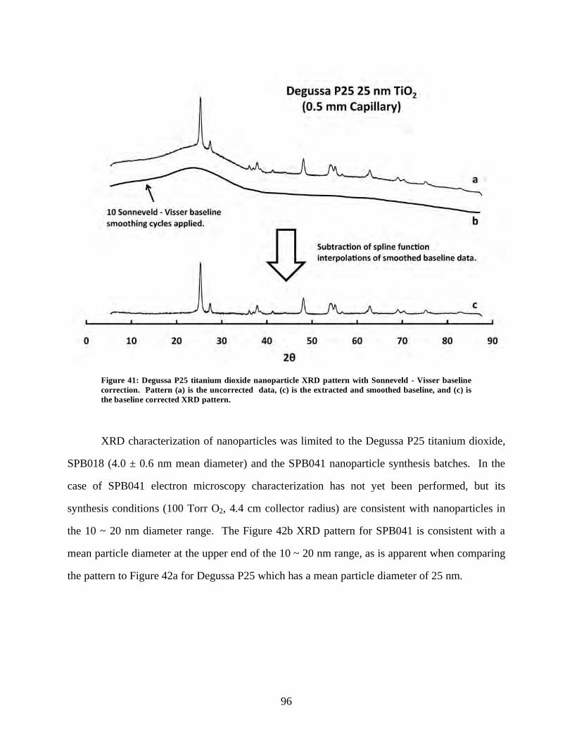
96
Figure 41: Degussa P25 titanium dioxide nanoparticle XRD pattern with Sonneveld - Visser baseline correction. Pattern (a) is the uncorrected data, (c) is the extracted and smoothed baseline, and (c) is the baseline corrected XRD pattern.
XRD characterization of nanoparticles was limited to the Degussa P25 titanium dioxide,
SPB018 (4.0 ± 0.6 nm mean diameter) and the SPB041 nanoparticle synthesis batches. In the
case of SPB041 electron microscopy characterization has not yet been performed, but its
synthesis conditions (100 Torr O2, 4.4 cm collector radius) are consistent with nanoparticles in
the 10 ~ 20 nm diameter range. The Figure 42b XRD pattern for SPB041 is consistent with a
mean particle diameter at the upper end of the 10 ~ 20 nm range, as is apparent when comparing
the pattern to Figure 42a for Degussa P25 which has a mean particle diameter of 25 nm.

97
Figure 42: X-ray diffraction nanoparticle characterization. Patterns are for (a) Deguss P25, (b) SPB041, and (c) SPB018 titanium dioxide. Reflections identified with ‘?’ are tentative.
The XRD pattern reflection assignments are based on the work of Zhou et al.211, where
Degussa P25 was characterized. The patterns in Figure 42 were offset from each other for clarity
in the pattern plot, but no other modification of the data has been performed. It is interesting to
note that for Figure 42c, from the 4.0 ± 0.6 nm diameter particles, the dominant titanium dioxide
polymorph appears to be rutile, with very little or no anatase present in the pattern. This
outcome would seem to be in conflict with the earlier observation that anatase is the
thermodynamically favored polymorph for particle diameters below 14 nm.81-83 This phenomena
might be a characteristic of particles made by laser vaporization synthesis, and it merits further
investigation.

98
3.3 FTIR Data Processing and Shallow Trap Energy Calculation
My calculation of titanium dioxide nanoparticle shallow trap state energy is based upon a
mathematical treatment of infrared spectra. Conduction band electron population effects on the
infrared spectrum baseline are observed over all infrared frequencies between 4000 to 1000 cm-1.
Although the temperature ramp spectra were recorded under vacuum, spectral absorbances from
residual water on the nanoparticles in the vacuum cell is still observed. For this reason I decided
to use a region of the infrared spectrum from 2600 to 1900 cm-1 for my calculations. This region
is isolated from hydrogen bonded OH absorbance over 3700 to 2600 cm-1 and water H-O-H
bending modes at 1650 cm-1.
The Mattson WinFirst spectroscopy software saves infrared spectra as space-delimited
ASCII text files. Each file contains several hundred data points, and collectively there were
approximately one hundred or more files to examine. My approach was to write a computer
program in G77 FORTRAN (WaveShave.f, Appendix 3) which used a text file list of data files
to direct sequential processing of spectra. Each data file on the list was opened and read by
WaveShave.f and rewritten as a second text file which only contained spectral data points
between my predefined range of infrared frequencies, 2600 to 1900 cm-1. When the file
processing run was complete, a new set of truncated infrared spectrum data files had been
created.
The association of infrared spectrum baseline area given in Equations (63) to (66) with
the Fermi-Dirac behavior of conduction band electrons requires an integrated area under the
spectrum baseline for each truncated spectrum file produced by data processing with
WaveShave.f. I wrote a second G77 FORTRAN program (TrapInt2.f, Appendix 4) which was
adopted from a program given in Nyhoff and Leestma’s FORTRAN 77 for Engineers and
Scientists.212 My program applied trapezoidal numerical integration to the truncated spectra
baselines previously generated by WaveShave.f. Trapezoidal integration is based upon the
approximation:

99
f (x)dx ≈Δx2a
b
∫ f (x0 ) + 2 f (x1) + 2 f (x2 ) + + 2 f (xn−1) + (xn )⎡⎣ ⎤⎦ (75)
where Δx = (b - a) / n and xi = a + iΔx.213 The variables a and b were the starting and ending
frequencies of the truncated spectrum, n was the number of data points contained within the data
file, and Δx was the spacing between absorbance data points within the file. Like WaveShave.f,
the program TrapInt2.f uses an ASCII text file containing a list of data files (those previously
generated by WaveShave.f) to direct processing. The integration results from the batch
processing are written to a single ASCII text file as a summary of data file names and their
associated integration result.
Following integration of the truncated FTIR spectra, a curve fit to the Fermi-Dirac
relation previously given in Equation (64) was necessary (see page 61). The baseline integration
areas were matched to their associated sample temperatures and these data were fit to the Fermi-
Dirac relation using a non-linear least squares technique described by Brown.214, 215 This curve
fit technique is performed with a spreadsheet constructed in Microsoft Excel®. Reiterative
processing of the data set within the spreadsheet is accomplished with the Solver® application
that is included with the spreadsheet program. The variables of the regression are the integrated
baseline area Z and the nanoparticle temperature T. The regression parameters are the
proportionality constant D and the shallow trap energy state Estate. An example of my
spreadsheet constructions is shown in Figure 43.

100
Figure 43: Nonlinear regression curve fit spreadsheet for the Fermi-Dirac relationship.
Brown’s approach is to use Solver® to reiteratively adjust the fit parameters specified by
the user while simultaneously seeking to maximize coefficient of determination, RSQ in Figure
43. For perfect correlation of the independent and dependent variables (T and Z in my work)
RSQ would be one. A summary of the regression results for the SPB018 (4.0 ± 0.6 nm)
nanoparticles is given in Table 3 and for the SPB020 (30 ± 10 nm) nanoparticles in Table 4.
Plots of the regression data sets and their fitted Fermi – Dirac trend lines are provided in Figure
44.

101
Regression Parameters
Data Set D (A.U.⦁⦁ cm2⦁ ne)
ESTATE (eV)
RSQ
11/30/07 3.48 x 10⁻¹⁸ 0.290 0.999
12/03/07 3.10 x 10⁻¹⁸ 0.277 0.996
12/04/07 1.22 x 10⁻¹⁷ 0.457 0.993
12/10/07 5.01 x 10⁻¹⁸ 0.302 0.992
12/20/07 7.14 x 10⁻¹⁸ 0.377 0.997
Mean (eV): 0.34
Standard Deviation (eV): 0.08
Table 3: Fermi - Dirac regression results for SPB018 (4.0 ± 0.6 nm) TiO2 nanoparticles.
Regression Parameters
Data Set D (A.U.⦁ cm2⦁ ne)
ESTATE (eV)
RSQ
12/05/07 9.84 x 10⁻¹⁸ 0.398 0.992
12/06/07 2.98 x 10⁻¹⁸ 0.259 0.976
12/18/07 2.65 x 10⁻¹⁸ 0.207 0.998
Mean (eV): 0.3
Standard Deviation (eV): 0.1
Table 4: Fermi - Dirac regression results for SPB020 (30 ± 10 nm) TiO2 nanoparticles.

102
Figure 44: Integrated area vs. temperature plots for 4 nm (circle symbols) and 30 nm (triangle symbols) TiO2. Trend lines are fitted Fermi – Dirac relation. Data sets designated with (a) were collected with cryogenic water trapping.

103
Chapter 4: Discussion of Results and Conclusions
4.1 Review of Research Objectives
Titanium dioxide nanoparticles catalyze oxidation-reduction chemistry by using external
energy inputs (heat or electromagnetic radiation) to promote electron transport between the
particle surface and adsorbates. This catalytic cycle is initiated by excitation of electrons to the
titania conduction band, causing the migration of both electrons and electron vacancies (i.e.
‘holes’) to the particle surface. Thermal excitation of electrons provides an alternative to high-
intensity ultraviolet irradiation of nanoparticles for promotion of adsorbate reaction catalysis.
The electrons entering the titania conduction band as the result of thermal excitation originate
from structural defects in the titanium dioxide crystal lattice structure that are collectively named
shallow trap states. Characterization of the energy requirements for thermal excitation of
electrons from these shallow trap states is important to understanding and optimizing titanium
dioxide nanoparticle catalysis. My work sought to determine the shallow trap state energies for
titanium dioxide nanoparticles that were formed through laser vaporization-condensation
synthesis techniques. My measurement of shallow trap state energies was accomplished through
collection of transmission infrared spectra of the nanoparticles over temperatures spanning 298
to 675 K, followed by evaluation of the spectroscopic data with an expression derived from
Fermi-Dirac electron theory.
4.2 Nanoparticle Sizes and Size Distributions
One early idea for directing the size of titanium dioxide nanoparticles produced from
laser vaporization was to vary the radial distance from the precursor material pellet to the
collector surface. By increasing the volume in which accreting particles could undergo collisions
with gaseous titanium dioxide species, it was hoped that larger particles could be generated.
Two hemispherical steel collector surfaces were prepared with radii of 2.3 and 6.3 cm.
The 4.0 cm difference in radii correspond to a volume difference of approximately 500 cm3.
Nanoparticle batches were prepared with each collector at a chamber pressure of 37 Torr. The

104
particle diameter data for these batches, SPB014 and SPB015 in Table 6 on page 127, suggests
that reducing the collector volume by approximately one-half liter had negligible effect on the
nanoparticle mean diameter. The difference in diameters between these batches was
approximately 8%. Electron micrographs for both batches are presented in Figure 45.
Figure 45: Transmission electron micrographs for SPB014 and SPB015 titanium dioxide nanoparticle batches. The precursor pellet to collector surface distance was (a) 6.3 cm and (b) 2.3 cm. Both syntheses conducted at 37 Torr O2 chamber pressure.
The effect of pressure manipulation on nanoparticle mean diameter is much easier to
discern. While the data in Table 6 for nanoparticle syntheses with the 4.4 cm radius collector at
different pressures is not well correlated (R2 = 0.86 in Figure 39), there is a monotonic increase
in particle diameter with increasing vaporization chamber pressure. There also is a trend of
increasing particle size distribution (note the increasing standard deviations with pressure in
Table 6).
As the chamber pressure increases, the mean free path of the gaseous species within the
chamber reduces. Atkins and de Paula note that mean free path reduces by one-half for each
doubling of pressure.90 For the Table 6 data vaporization experiments were performed at
pressures between 1 and 500 Torr O2. The difference in these pressures represents

105
approximately nine doublings of pressure. The corresponding nine reductions of the mean free
path by factors of one-half would have a cumulative effect of a 2 x 10⁻³ reduction. This
magnitude of mean free path reduction translates into greatly increased collision frequency
between accreting nanoparticles and gaseous material from the liquefied precursor pellet.
Increased collisions in the gas phase from increased chamber pressure also provide a
greater opportunity for Maxwell-Boltzmann statistics to broaden the distribution of particle
diameters. The gaseous species within the vaporization chamber partitions in a Boltzmann
distribution at any of the pressures used for nanoparticle synthesis. At higher pressures, with
increased collision frequency, that distribution of energies is imparted upon the accreting
particles. The result is that the particles acquire a Boltzmann distribution of energies which
affects their number of collisions. For example, a particle impacted by more high kinetic energy
particles will itself acquire a higher kinetic energy than an identical particle that experienced
fewer high energy impacts. The distribution of nanoparticle speeds leads to a distribution of
growth rates that broaden the nanoparticle size distribution. This effect appears to be directly
proportional to the vaporization chamber pressure.
4.3 Shallow Trap State Energy Measurements
The Fermi-Dirac regression results for 4 nm and 30 nm particles were considered
separately in Table 3 and Table 4 respectively, on page 101. Chestnoy et al. 216 observed that
when the diameter of 3 nm cadmium sulfide nanoparticles approached the diameter of their
shallow trap states, strong mixing of the trap state and the conduction band wavefunctions occur.
This mixing suggests that there may be a size effect on the shallow trap state energies observed
for particles of greatly different size. My observations do not indicate a size effect on shallow
trap state energies. The mean ESTATE values in Table 3 and Table 4 are essentially the same (0.34
± 0.08 and 0.3 ± 0.1 eV respectively). However, it may be inappropriate to consider this
comparison as a test of size effects on shallow trap state energies, as the larger particles
represented in Table 4 had a much larger distribution of diameters than the particles in Table 3.

106
Shallow trap state energies reported by different researchers for titanium dioxide span the
range of 0.1 to 1.1 eV.99, 100, 217-221 The techniques used to make these measurements included
thermoluminescence and diffuse reflectance spectroscopy, as well as electrochemistry and purely
theoretical, computer simulation. My 0.3 ~ 0.34 eV range of values from infrared spectroscopy
compare favorably with some of these literature values that are presented in Table 5.
Researcher Shallow Trap State Gap,-s (eV)
Ghosh et al.99 0.27, 0.28, 0.32, 0.39, 0.48, 0.56, 0.60, 0.62, 0.76, 0.87
Frindell et al.217 0.1 ~ 0.6
Lagemaat et al.100 0.4 a
Szczepankiewicz et al.218 0.42
Valentin et al.219 0.9, 1.1
Warren et al.220 0.1
Peter et al.221 0.1 ~ 0.25
Table 5: Survey of reported values for titanium dioxide shallow trap state energy gap, relative to bottom edge of conduction band. (a) indicates a calculated value.
The placement of the shallow trap state energy within the context of other features of the
titanium dioxide energy band diagram is shown in Figure 46. As previously noted in Table 1 on
page 30, the gap separating the bottom of the conduction band and the top of the valence band is
approximately 3.0 eV. The Fermi-Dirac expression presented in Equation (64) that relates the
integrated infrared baseline area to conduction band electron density was derived with an
assumption that the E variable in the exponential term represents the electron trap energy closest
to the conduction band, i.e. a shallow trap state. The energy difference between the conduction
band and this shallow trap state is also indicated in Figure 46. Other features noted in this figure

107
are the vacuum energy level energy (Evacuum) for titania, i.e. the energy at which an electron is
completely removed from the semiconductor, and the Fermi energy (EFermi).
Figure 46: The shallow trap state energy difference of titanium dioxide relative to the band structure.
Accurate placement of the Fermi energy for a semiconductor nanoparticle such as
titanium dioxide is difficult. Experimental approaches to measuring Fermi energy have included
electron spectroscopy techniques98 and observation of electric current–voltage behavior at a
junction between semiconductors of known and unknown Fermi energies.222 Hayes and
Stoneham noted that for a pure, undoped semiconductor the Fermi energy is located in the
middle of the band gap, but when dopants are introduced the Fermi level is increased above the
midpoint of the gap.223 Göpel et al. placed the Fermi level less than 1 eV below the conduction
band.98 Given that electron trap state populations within the band gap are variable, location of
the Fermi energy for a nanoparticle without direct measurement is limited to estimates.
4.4 Estimation of Electron Shallow Traps Population
Titanium cations are the most likely locale of titanium dioxide nanoparticle shallow
electron traps. While electron micrographs such as Figure 45 on page 104, Appendix 6 Figure

108
50 on page 128, and Appendix 7 Figure 51 on page 129 give the appearance that nanoparticles
are smooth spheres, at the atomic scale the surface of the particle contains numerous steps and
corners where titanium cations are incompletely coordinated with oxygen anions. This particle
surface atomic ‘roughness’ is discernable in the high resolution transmission electron micrograph
shown in Appendix 8 Figure 52. Larger particles containing multiple titania polymorph phases
may have grain boundaries that also can contribute irregularities in cation coordination leading to
electron trapping.224 Coordinate unsaturated cations at the particle surface are particularly
susceptible to capture of electrons from adsorbates, with a reduction of oxidation state from Ti4+
to Ti3+. Loss of oxygen from titanium dioxide with an accompanying formation of Ti3+ as shown
in Figure 15 on page 35 is also more likely to occur at the particle surface. Also, Lagemaat et al.
noted that lattice defect electron trap sites are presumed to be located on the surfaces of
nanoparticles because of their high surface-to-volume ratio.100
An attempt to estimate the number of shallow trap sites could begin with the Equation
(64) Fermi-Dirac expression. While this expression gave estimates of the shallow trap energy
level that were in reasonable agreement with the work of other researchers, as shown in Table 5,
closer examination of Equation (64) does not offer a means to mathematically estimate the total
number of trap sites present on a titania nanoparticle particle.
Consider the example of a 4 nm diameter titania particle that is composed entirely of the
rutile polymorph (density = 0.235 g ⦁ cm-3)84. Evaluation of Equation (61) for Estate = 0.3 eV at a
temperature of 298 K indicates that approximately 1.69 x 10¹⁶ electrons are excited into the
conduction band for one gram of nanoparticles (See Appendix 9 on page 131). Implicit in this
example is the assumption that the number of electrons entering the conduction band equals the
number of electron-donor shallow trap sites. The Fermi-Dirac trends in Figure 44 demonstrate a
correlation between nanoparticle temperature and FTIR integrated baseline area. This increase
in integrated FTIR baseline area is an indication of increased conduction band electron
population. If evaluation of Equation (61) is repeated under similar constraints, with the
nanoparticle temperature changed to 675 K, the new conduction band electron population is

109
approximately 1.51 x 10¹⁸ electrons per gram of rutile nanoparticles.. If the number of electrons
in the conduction band is equal or proportional to the number of shallow trap sites, there should
exist a temperature for Equation (61) where a maximum conduction band electron population
occurs. The number of conduction band electrons at this temperature could serve as an estimate
of the number of electron trap states. This maxima should be accessible through evaluation of
the roots of a first-order derivative of Equation (61).
The first-order derivative of Equation (61) with respect to the independent temperature
variable is:
dNCB(T )dT
= B2T 1/ 2
⎛⎝⎜
⎞⎠⎟
2CEState + 3T( ) Exp −CEState
T⎛
⎝⎜⎞
⎠⎟ (76)
where B and C are aggregate constants, Estate is the shallow trap state energy, and T is the
thermodynamic temperature. The first multiplied term of Equation (76) and the right-most
exponential term can only reach a zero value at an infinite temperature, as shown in Equations
(77) and (78). The remaining middle term of Equation (76) achieves a zero value at a negative
thermodynamic temperature value, which has no physical meaning, as shown in Equation (80).
These results exclude a purely analytical solution to estimation of shallow trap population from
the Equation (61) Fermi-Dirac expression.
B2T 1/ 2 → 0
T→∞
(77)
Exp −
CEState
T⎛
⎝⎜⎞
⎠⎟→ 0
T→∞
(78)
2CEState + 3T = 0 (79)

110
T = − 2
3CEState (80)
It is intuitive that a nanoparticle has a finite number of shallow state trapped electrons.
An experimental determination of the number of trap states from recording additional infrared
spectra at temperatures above 675 K may not succeed at determination of an electron thermal
excitation maximum. Excessive heating of titania nanoparticles will lead to the creation of
additional oxygen vacancies with creation of new trap sites. Annealing of titanium dioxide will
alter the polymorph composition of mixed phase nanoparticles, obscuring the trap state
population of the starting material.
4.5 FTIR Surface Chemistry Observation and Electron Monitoring
Infrared spectroscopy is an indispensable tool for the study of nanoparticle surfaces.
FTIR techniques provide a fast, nondestructive method for identification of surface adsorbates.
Shifts of characteristic infrared absorbance frequencies also provide information about the
surface of adsorption in addition to qualitative identification of the adsorbates. For example, a
red-shifted infrared absorbance frequency (i.e. shifted to lower value, corresponding to a longer
wavelength) is an indication of weakened bonding in the adsorbate. This condition could arise
from withdrawal of adsorbate electron density through bonding to a surface Lewis acid site.
Alternately, population of adsorbate antibonding molecular orbitals with electrons from the
adsorption surface could weaken the adsorbate bond and lead to a red-shifted absorbance
frequency. The complementary utility of using the same infrared spectroscopy to simultaneously
monitor electron population transitions is that it provides information to discern which of these
cases might be applicable.
Infrared monitoring of electron population offers further information, beyond correlation
of adsorbate IR frequency shifts. A common reaction mechanism step for catalytic adsorbate
oxidation on reducible oxide surfaces (in the absence of gaseous oxygen) is lattice oxygen
extraction through the Mars and van Krevelen mechanism.225-229 For titanium dioxide, this
lattice oxygen extraction is accompanied by the formation of additional, populated shallow

111
trapped electrons (see Figure 15 on page 35) which are thermally excited to the conduction band.
Through IR monitoring of electron populations, a lattice oxygen extraction mechanism could be
identified for adsorbate oxidation. Similar scenarios can be described where nanoparticle
electron population can be used to monitor surface coverage by electron withdrawing adsorbates
(e.g. molecular O2 or H2O) or their displacement from the particle surface by reactive adsorbates.
4.6 Future Work
The FTIR vacuum cell offers a highly controlled environment to observe nanoparticle
surface chemistry. This control of experimental variables comes at a cost of time. The
procedures necessary to place new samples into the cell and condition them can require days to
weeks before the cell and the samples within it are ready for experimental work. In addition to
slow throughput, observation of nanoparticle catalysts under high vacuum is not representative
of typical catalyst applications .
Dr. Dimitar Panayotov has designed and had fabricated a quartz flow cell for FTIR
nanoparticle observation at nearly atmospheric pressure. This spectrometer cell is designed to
contain a square tungsten mesh, identical to the material used as a nanoparticle carrier in the
FTIR vacuum cell. With resistive heating, the FTIR flow cell is capable of conducting
nanoparticle catalysis studies that parallel the vacuum cell studies with a continually replenished
supply of reactant.
The geometry of the flow cell is arranged in a diamond orientation, with gas flow into
and out of the cell occurring at opposite corners of the gas cavity, as shown in Figure 47. The
gas expansion zone, located at the widest part of the gas cavity, falls directly above the location
of the nanoparticle sample mounted within the cell. At this region of gas expansion, the linear
velocity of the gas decreases, affording greater time for gas – nanoparticle interaction.

112
Figure 47: Nanoparticle FTIR flow cell. The photographic inset in the upper left corner is the prototype flow cell and flow cell mounting bracket. The circular region in the photograph is a sample of Degussa P25 titanium dioxide nanoparticles.
The FTIR flow cell is attached to an external gas routing system that allows for insertion
of gaseous compounds or vaporized liquids into the carrier gas stream flowing through the cell.
We hope to use this apparatus to examine chemical warfare agents interaction with nanoparticle
system under conditions more accurately representative of applied usage of the catalysts.
Another advantage of the gas flow cell approach is quick sample through put. Because
the flow cell operates at approximately atmospheric pressure, its gas seals can be less robust than
those of a high vacuum chamber. With less stringent gas seal requirements, the flow cell can be
rapidly set up or disassembled. It is hoped than when the flow cell apparatus is fully operational,
several nanoparticle samples per week can be examined as opposed to one or two sets of
nanoparticles per month for the FTIR vacuum cell. With this level of sample through put, the
flow cell can serve as screening tool to identify nanoparticle samples that show promising
characteristics which merit more detailed examination under high vacuum conditions.

113
Other interests include improvement of the laser vaporization procedure for nanoparticle
synthesis. I would like to explore application of filter trapping of nanoparticles , electrostatic
nanoparticle capture, and size segregation of particles to obtain more monodisperse samples of
particles for particle size effect studies.

Appendix A: Density of States Derivation
114
Blakemore230 presented this derivation for calculating the density of electron states within
a crystal lattice. Several assumptions are implicit in this derivation:
• Motions of electrons are restricted to the volume of the crystal.
• There are a finite number of electron states for the specified range of energies and momenta.
• The crystal lattice is much larger than the sizes if its component atoms.
• The electron ‘sees’ a homogeneous environment (uniform potential field) within the lattice.
• The electron potential energy V is zero within the lattice and infinite outside the lattice.
• The effects of the crystal surfaces are negligible.
• The electron wave function Ψ is periodic along each Cartesian axis of the lattice.
An electron delocalized from its original atom within a crystal lattic is free to move
within the confines of that lattice space. Such an electron has momentum, represented by the
vector ρ→→ . Quantum mechanics govern the actions of delocalized electrons and electrons possess
wave-particle duality. The de Broglie wavelength of an electron is:
λ =
hρ
=h
mev (81)
where ρ is the magnitude of the vector ρ→ , me is the effective electron mass, and h is Planck’s
constant. Each electron can also be represented by a wave-vector:
k =
ρwhere =
h2π
(82)
The wave-vector k→
with scalar components kx, ky, and kz, exists in a Cartesian coordinate vector
space that is constructed by drawing a vector k→
from the origin to a point k. The spherical
surface formed by all wave-vectors k→
for a given electron represents the degenerate energy
states for that electron. Figure 48 shows k→
-vector space for an electron:

Appendix A: Density of States Derivation (Continued)
115
Figure 48: k
→ vector space for an electron.
For an electron represented by a k→→
wave-vector the following conditions must be true for the
vector components:
ρx = kx ρy = ky ρz = kz (83)
The kinetic energy of the electron is:
E =
2
2me
kx2 + ky
2 + kz2( ) =
2k 2
2me
(84)
The time independent Schrödinger equation for the electron within the crystal lattice is:
−
2
2me
∇2Ψ = EΨ (85)
An acceptable solution for the wave function Ψ is
Ψ = C exp(ik • r ) (86)

Appendix A: Density of States Derivation (Continued)
116
where r→→
is the radial displacement vector for k→
. The wave function Ψ is defined such that the
probability of finding an electron within a volume element τ is given by Ψ
2dτ . The periodicity
of the wave function Ψ is L. Acceptable solutions for the wave function Ψ correspond to
electron states within the lattice, if the following conditions are true:
kx = nx
2πL
, ky = ny
2πL
, kz = nz
2πL
(87)
where nx, ny, and nz are integers and can assume the values 0, ±1, ±2, ±3, …,±n.
The Heisenberg uncertainty principle requires that if an electron position is determinate
in L the electron must be indeterminate in momentum and wave-vector:
Δρ =
hL
and Δk =2πL
(88)
Only specific positions in k→
-space correspond to acceptable wave functions and each acceptable
position is within a cell of volume (2π/L)3. Figure 49 shows a range of such positions in the x-y
plane and an example of a cell:
Figure 49: Acceptable wave function positions in the x-y plane.
The number of electron states within a sphere of radius k is found by dividing the volume of the
sphere by the volume of a single wave function cell:
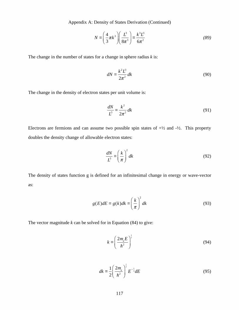
Appendix A: Density of States Derivation (Continued)
117
N =
43πk 3⎛
⎝⎜⎞⎠⎟
L3
8π 3
⎛
⎝⎜⎞
⎠⎟=
k 3L3
6π 2 (89)
The change in the number of states for a change in sphere radius k is:
dN =
k 2 L3
2π 2 dk (90)
The change in the density of electron states per unit volume is:
dNL3 =
k 2
2π 2 dk (91)
Electrons are fermions and can assume two possible spin states of +½ and -½. This property
doubles the density change of allowable electron states:
dNL3 =
kπ
⎛⎝⎜
⎞⎠⎟
2
dk (92)
The density of states function g is defined for an infinitesimal change in energy or wave-vector
as:
g(E)dE = g(k)dk =
kπ
⎛⎝⎜
⎞⎠⎟
2
dk (93)
The vector magnitude k can be solved for in Equation (84) to give:
k =
2meE2
⎛
⎝⎜⎞
⎠⎟
12
(94)
dk =
12
2me2
⎛
⎝⎜⎞
⎠⎟
12
E− 12 dE (95)
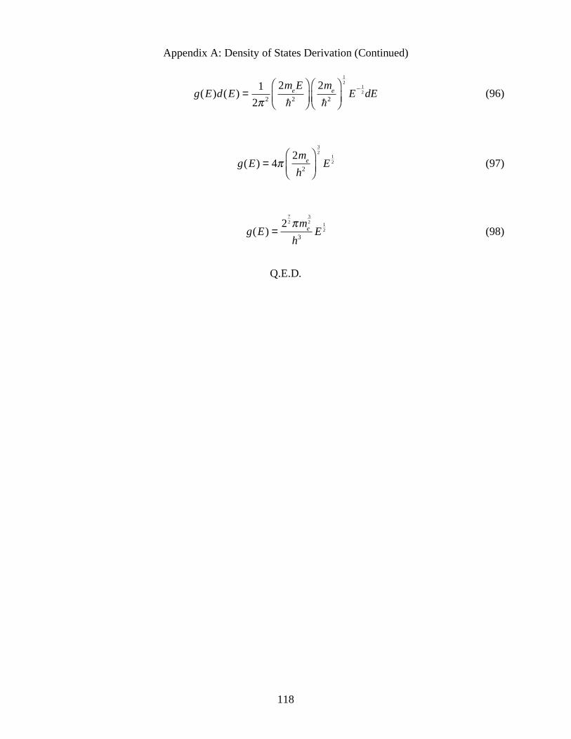
Appendix A: Density of States Derivation (Continued)
118
g(E)d(E) =
12π 2
2meE2
⎛
⎝⎜⎞
⎠⎟2me
2
⎛
⎝⎜⎞
⎠⎟
12
E− 12 dE (96)
g(E) = 4π
2me
h2
⎛
⎝⎜⎞
⎠⎟
32
E12 (97)
g(E) =
272πme
32
h3 E12 (98)
Q.E.D.

Appendix B: Fermi – Dirac Distribution Derivation
119
Blakemore230 presented this derivation for the Fermi-Dirac distribution Law. This
derivation requires several assumptions:
• A very large number of electrons exist.
• The electrons at a given energy are indistinguishable.
• The number of electrons in the system and the total energy of all electrons is fixed.
• The system is in thermal equilibrium.
For gi electron states with Ei energies, ni represents the number of occupied electron states and gi
– ni represents the number of unoccupied states. The number of distinguishable distributions is:
wi =
gi !ni !(gi − ni )
(99)
In addition to the gi occupied electron states at energies Ei, there are other states at higher and
lower energies. The combination of the wi electron states and these other states comprises the
system. The total number of distinguishable system distributions w is:
w = wr =
r∏ gr !
nr !(gr − nr )r∏ (100)
The transitions of electrons between states are subject to these conditions:
n = nr
r∑ (101)
nE = nr
r∑ Er (102)
The most probable distribution of electrons in states at thermal equilibrium:

Appendix B: Fermi – Dirac Distribution Derivation (Continued)
120
δwδnr
= 0 (103)
The factorials of very large numbers in the probability Equations (99) and (100) can be estimated
with Stirling’s approximation:
ln y!= y ln y − y for y 1 (104)
Equation (100) becomes:
ln w = gr ln gr − nr ln nr − gr − nr( ) ln gr − nr( )⎡⎣ ⎤⎦
r∑ (105)
Rewrite conditions (101) and (102) as:
n − nr = 0
r∑ (106)
nE − nr Er
r∑ = 0 (107)
The maximum value of ln w, subject to conditions (106) and (107) is found by the method of
Lagrange undetermined multipliers. At a maximum for ln w:
δδnr
ln w +α n − nrr∑⎛
⎝⎜⎞⎠⎟
+ β nE − nr Err∑⎛
⎝⎜⎞⎠⎟
⎡
⎣⎢
⎤
⎦⎥ = 0 (108)
Differentiation of each term in (108) equation reference goes here gives:
δδnr
ln w = lngr − nr
nr
⎛
⎝⎜⎞
⎠⎟ (109)

Appendix B: Fermi – Dirac Distribution Derivation (Continued)
121
δδnr
α n − nrr∑⎛
⎝⎜⎞⎠⎟
⎡
⎣⎢
⎤
⎦⎥ = −α (110)
δδnr
= β nE − nr Err∑⎛
⎝⎜⎞⎠⎟
⎡
⎣⎢
⎤
⎦⎥ = −βEr (111)
Equation (108) becomes:
ln
gr − nr
nr
⎛
⎝⎜⎞
⎠⎟= α + βEr (112)
nr
gr
=1
1+ exp(α + βEr ) (113)
For any of the states gr within the system, the probability that an nr particle at energy Er occupies
that state is:
f (Er ) =
11+ exp(α + βEr )
(114)
If we allow α = EF/kBT where EF is defined as the Fermi energy and kB is the Boltzmann
constant, the energy of the highest occupied state at T = 0K and β = 1/(kBT):
f (Er ) =1
1+ expEr − EF
kBT⎛
⎝⎜⎞
⎠⎟
(115)
Q.E.D.

Appendix C: FORTRAN Program WaveShave.f
122
PROGRAM WaveShave INTEGER NumPoints, N, EOF1, EOF2 REAL ReadFreq, ReadAbs, LowFreq, HighFreq CHARACTER*12 IRFileIn, IRFileOut, Spacer Spacer = ' ' * Frequency Filter Values * *********************** LowFreq = 1.9E3 HighFreq = 2.6E3 OPEN (Unit=1, File='FILELIST.TXT', Status='OLD') * Read in the data files to integrate EOF1 = 0 DO WHILE (EOF1 .EQ. 0) READ (1, FMT = '(A12)', IOSTAT=EOF1) IRFileIn * Check for EOF * IF (EOF1 .EQ. -1) THEN * GO TO 700 * END IF PRINT *, ' ' PRINT *, IRFileIn PRINT *, '************' * Open the input file OPEN (Unit=2, File=IRFileIn, Status='OLD') * Open the output file as a TXT type. IRFileOut = IRFileIn(1:10) // 'XT' EOF2 = 0 OPEN (Unit=3, File=IRFileOut, Status='NEW') DO WHILE (EOF2 .EQ. 0) ReadFreq = 0 ReadAbs = 0 500 READ (2, *, IOSTAT=EOF2) ReadFreq, ReadAbs * Check for EOF IF (EOF2 .EQ. -1) THEN GO TO 550 END IF * Check for data points under the low wavenumber IF (ReadFreq .LT. LowFreq) THEN GO TO 500 END IF * Check for data points under the high wavenumber IF (ReadFreq .GT. HighFreq) THEN GO TO 500 END IF PRINT *, ReadFreq, Spacer, ReadAbs WRITE (3, *) ReadFreq, ReadAbs 550 CLOSE (2)

Appendix C: FORTRAN Program WaveShave.f (Continued)
123
CLOSE (3) 600 END DO 700 CLOSE (1) CLOSE (3) END

Appendix D: FORTRAN Program Trapint2.f
124
PROGRAM Trapint2 INTEGER NumPoints, N, EOF1, EOF2, Count1, Count2, NumDeltaFreq REAL Freq, Freq0, Freq1, DeltaFreq, SumDeltaFreq, Abs, LeftAbs, RightAbs, IntArea REAL ReadFreq, ReadAbs CHARACTER*12 IRFile, Spacer Count1 = 0 Count2 = 0 Spacer = ' ' * Open the results output file OPEN (Unit=3, File='INTRESULT.TXT', Status='NEW') OPEN (Unit=1, File='FILELIST.TXT', Status='OLD') * Read in the data files to integrate EOF1 = 0 DO WHILE (EOF1 .EQ. 0) READ (1, FMT = '(A12)', IOSTAT=EOF1) IRFile PRINT *, ' ' PRINT *, IRFile PRINT *, '************' Count1 = Count1 + 1 * Count the number of data points in file EOF2 = 0 Count2 = 0 OPEN (Unit=2, File=IRFile, Status='OLD') DO WHILE (EOF2 .EQ. 0) Count2 = Count2 + 1 ReadFreq = 0 ReadAbs = 0 READ (2, *, IOSTAT=EOF2) ReadFreq, ReadAbs IF (EOF2 .EQ. -1) THEN GO TO 1000 ENDIF END DO 1000 NumPoints = Count2 CLOSE (2) * Compute average DeltaFreq EOF2 = 0 Count2 = 0 Freq0 = 0 Freq1 = 1 DeltaFreq = 0 SumDeltaFreq = 0 NumDeltaFreq = 0 OPEN (Unit=2, File=IRFile, Status='OLD') DO WHILE (EOF2 .EQ. 0)

Appendix D: FORTRAN Program Trapint2.f (Continued)
125
1100 ReadFreq = 0 ReadAbs = 0 READ (2, *, IOSTAT=EOF2) ReadFreq, ReadAbs Count2 = Count2 + 1 * First wavenumber IF (Count2 .EQ. 1) THEN Freq1 = ReadFreq GO TO 1100 END IF * Last wavenumber IF (Count2 .EQ. NumPoints) THEN GO TO 1500 END IF Freq0 = Freq1 Freq1 = ReadFreq DeltaFreq = Freq1 - Freq0 NumDeltaFreq = NumDeltaFreq + 1 SumDeltaFreq = SumDeltaFreq + DeltaFreq END DO 1500 DeltaFreq = SumDeltaFreq / NumDeltaFreq CLOSE (2) * Integrate the data file EOF2 = 0 Count2 = 0 IntArea = 0 OPEN (Unit=2, File=IRFile, Status='OLD') DO WHILE (EOF2 .EQ. 0) 1550 Count2 = Count2 + 1 ReadFreq = 0 ReadAbs = 0 READ (2, *, IOSTAT=EOF2) ReadFreq, ReadAbs IF (Count2 .EQ. 1) THEN IntArea = IntArea + ReadAbs GO TO 1550 END IF IF (Count2 .EQ. NumPoints) THEN IntArea = IntArea + ReadAbs GO TO 1600 END IF IntArea = IntArea + (2*ReadAbs) PRINT '(I5.4, A2, E15.7, A2, E15.7, A2, E25.10, A2, E15.7)', Count2, Spacer, DeltaFreq, Spacer, IntArea, Spacer, ReadFreq, Spacer, ReadAbs END DO * Compute the trapezoidal integral 1600 IntArea = (IntArea/2)*DeltaFreq PRINT *, '==========================='

Appendix D: FORTRAN Program Trapint2.f (Continued)
126
PRINT '(E20.10)', IntArea WRITE (3, '(A12, E20.10)') IRFile, IntArea CLOSE (2) IF (EOF1 .EQ. -1) THEN GO TO 2000 END IF 1800 END DO 2000 CLOSE (1) CLOSE (3) END

Appendix E: Nanoparticle Size Measurement Data Summary
127
Nanoparticles Pellet to Collector
(cm)
O2 Press. (Torr)
Number of Measurements
Mean Diam. (nm)
Standard Deviation
(nm)
SPB013 4.4 1 235 7 1
SPB016 4.4 1 105 5 1
SPB017 4.4 1 172 4.8 0.9
SPB018 a 4.4 1 88 4.0 0.6
SPB024 4.4 5 111 5 1
SPB029 4.4 5 97 6 1
SPB022 4.4 10 97 6 1
SPB023 4.4 55 120 12 3
SPB025 4.4 90 62 12 3
SPB011 4.4 100 334 20 5
SPB019 4.4 200 147 22 7
SPB026 4.4 200 156 14 4
SPB037 4.4 200 296 27 9
SPB040 4.4 200 226 20 6
SPB027 4.4 310 49 24 6
SPB028 4.4 410 183 30 10
SPB020 b 4.4 500 192 30 10
SPB014 6.3 37 369 13 3
SPB015 2.3 37 247 12 4
a Used for Fermi – Dirac regressions, vacuum cell sample S1 b Used for Fermi – Dirac regressions, vacuum cell sample S1
Table 6: TiO2 nanoparticle size measurement data.

Appendix F: SPB018 Transmission Electron Micrograph
128
Figure 50: TEM micrograph for SPB018 4.0 ± 0.6 nm titanium dioxide nanoparticles. Inset is a histogram of manual particle diameter measurements. Labels on particles are diameter measurement flags.

Appendix G: SPB020 Transmission Electron Micrograph
129
Figure 51: TEM micrograph for SPB020 30 ± 10 nm titanium dioxide nanoparticles. Inset is a histogram of manual particle diameter measurements. Labels on particles are diameter measurement flags.

Appendix H: SPB018 High Resolution Transmission Electron Micrograph
130
Figure 52: High resolution micrograph of SPB018 titanium dioxide nanoparticles.

Appendix I: Conduction Band Electron Population Calculation
131
This appendix outlines the details of the calculation for the number of electrons excited
into the conduction band for a 4 nm (4 x 10⁻⁹ m) diameter titanium dioxide nanoparticle
composed of the rutile polymorph (density = 0.235 g ⦁ cm-3)84 with Estate = 0.3 eV. The density
of conduction band electrons is determined from Equation (61):
NCB (E) = BT 3/2 Exp
−CEState
T⎛
⎝⎜⎞
⎠⎟where B =
25/2 meπkB( )h3 and C = 1
2kB
The aggregate constants B and C are evaluated:
B =25/2 9.1094 ×10⁻³¹kg( ) 3.1416( ) 1.3807 ×10⁻²³ J • K −1( )
6.6261×10⁻³⁴ J • s( )3
1J = 1N • m = 1 kg • m• s−2( )• m = 1kg • m2 • s−2
B = 4.8296 ×10²¹ K − 2
3 • m−3( ) 1m100cm
⎛⎝⎜
⎞⎠⎟
3
B = 4.8296 ×10¹⁵ K − 32 • cm−3
C = 1
2 1.3807 ×10⁻²³ kg • m2 • s−2 • K −1( )
1eV = 1.6022 ×10⁻¹⁹ J
C = 12 1.3807 ×10⁻²³ J • K −1( )
⎡
⎣⎢⎢
⎤
⎦⎥⎥
1.6022 ×10⁻¹⁹ J1eV
⎛
⎝⎜⎞
⎠⎟
C = 5.8021×10³ K • eV −1
For temperature T = 298 K, Equation (61) is evaluated:
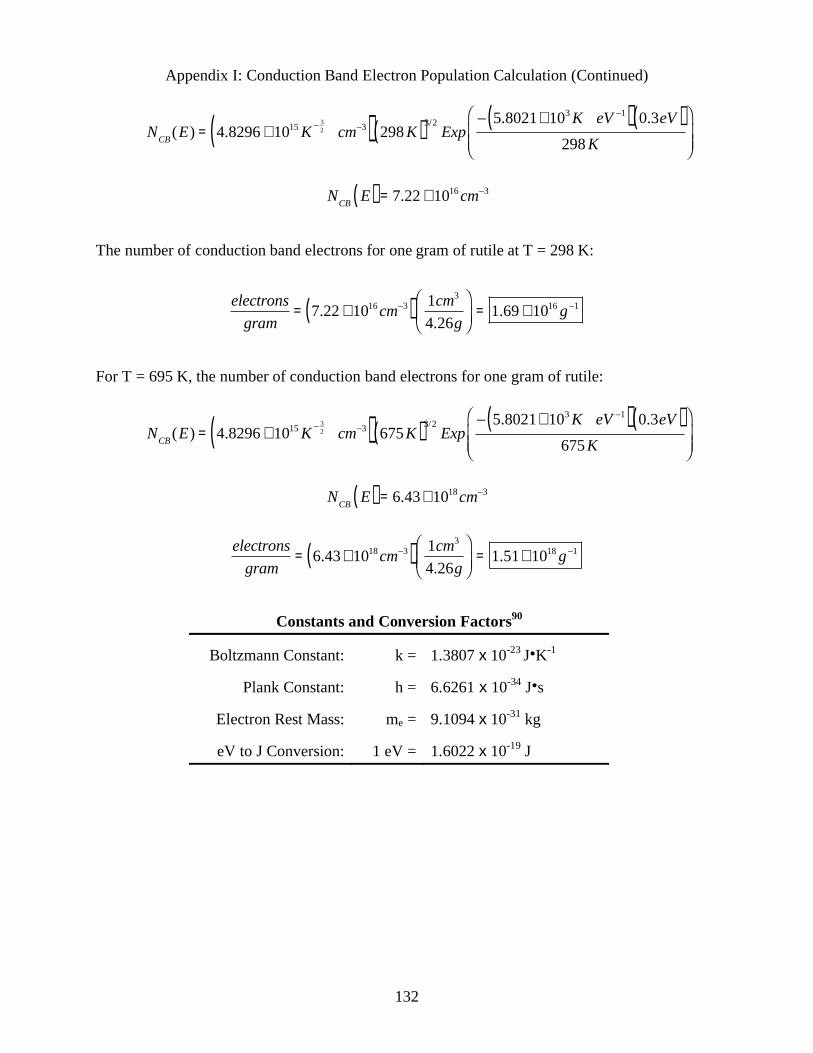
Appendix I: Conduction Band Electron Population Calculation (Continued)
132
NCB (E) = 4.8296 ×10¹⁵ K − 32 • cm−3( ) 298 K( )3/2
Exp− 5.8021×10³ K • eV −1( ) 0.3eV( )
298 K
⎛
⎝⎜⎜
⎞
⎠⎟⎟
NCB E( ) = 7.22 ×1016 cm−3
The number of conduction band electrons for one gram of rutile at T = 298 K:
electronsgram
= 7.22 ×1016 cm−3( ) 1cm3
4.26g⎛
⎝⎜⎞
⎠⎟= 1.69 ×10¹⁶ g−1
For T = 695 K, the number of conduction band electrons for one gram of rutile:
NCB (E) = 4.8296 ×10¹⁵ K − 32 • cm−3( ) 675 K( )3/2
Exp− 5.8021×10³ K • eV −1( ) 0.3eV( )
675 K
⎛
⎝⎜⎜
⎞
⎠⎟⎟
NCB E( ) = 6.43×1018 cm−3
electronsgram
= 6.43×1018 cm−3( ) 1cm3
4.26g⎛
⎝⎜⎞
⎠⎟= 1.51×10¹⁸ g−1
Constants and Conversion Factors90
Boltzmann Constant: k = 1.3807 x 10⁻²³ J⦁K-1
Plank Constant: h = 6.6261 x 10⁻³⁴ J⦁s
Electron Rest Mass: me = 9.1094 x 10⁻³¹ kg
eV to J Conversion: 1 eV = 1.6022 x 10⁻¹⁹ J

References
133
1. Hammer, B.; Nørskov, J. K., Why gold is the noblest of all the metals? Nature 1995, 376, 238-240.
2. Ionization Energies of Atoms and Atomic Ions. In CRC Handbook of Chemistry and Physics 88th Edition (Internet Version 2008), Lide, D. R., Ed. CRC Press/Taylor and Francis: Boca Raton, FL, 2008.
3. Electrical Resistivity of Pure Metals. In CRC Handbook of Chemistry and Physics 88th Edition (Internet Version 2008), Lide, D. R., Ed. CRC Press/Taylor and Francis: Boca Raton, FL, 2008.
4. Bond, G. C., Catalysis by Gold. Cat. Rev. - Sci. Eng. 1999, 41 (3&4), 319-388.
5. Haruta, M., When gold is not noble: Catalysis by nanoparticles. Chemical Record 2003, 3 (2), 75-87.
6. Panayotov, D. A.; Yates, J. T., Spectroscopic detection of hydrogen atom spillover from au nanoparticles supported on TiO2: Use of conduction band electrons. Journal of Physical Chemistry C 2007, 111 (7), 2959-2964.
7. Sakurai, H.; Haruta, M., Carbon-Dioxide and Carbon-Monoxide Hydrogenation over Gold Supported on Titanium, Iron, and Zinc-Oxides. Applied Catalysis a-General 1995, 127 (1-2), 93-105.
8. Newman, J. D. S.; Roberts, J. M.; Blanchard, G. J., Optical organophosphate/phosphonate sensor based upon gold nanoparticle functionalized quartz. Anal. Chim. Acta 2007, 602 (1), 101-107.
9. Newman, J. D. S.; Roberts, J. M.; Blanchard, G. J., Optical organophosphate sensor based upon gold nanoparticle functionalized fumed silica gel. Anal. Chem. 2007, 79 (9), 3448-3454.
10. Simonian, A. L.; Good, T. A.; Wang, S. S.; Wild, J. R., Nanoparticle-based optical biosensors for the direct detection of organophosphate chemical warfare agents and pesticides. Anal. Chim. Acta 2005, 534 (1), 69-77.
11. Panayotov, D. A.; Morris, J. R., Thermal Decomposition of a Chemical Warfare Agent Simulant (DMMP) on TiO2: Production of Trapped Electrons during Reactions with Lattice Oxygen Virginia Tech:
Blacksburg, VA, 2009.
12. Panayotov, D. A.; Morris, J. R., Catalytic Degradation of a Chemical Warfare Agent Simulant: Reaction Mechanisms on TiO2-Supported Au Nanoparticles. J. Phys. Chem. C 2008, (112), 7496-7502.
13. Sagatelian, Y.; Sharabi, D.; Paz, Y., Enhanced photodegradation of diisopropyl methyl phosphonate by the “Adsorb & Shuttle” approach. Journal of Photochemistry and Photobiology A: Chemistry 2005, (174), 253-260.

References
134
14. Obee, T. N.; Satyapal, S., Photocatalytic decomposition of DMMP on titania. Journal of Photochemistry and Photobiology a-Chemistry 1998, 118 (1), 45-51.
15. Daoud, W. A.; Turner, M. L., Effect of interfacial properties and film thickness on device performance of bilayer TiO2-poly(1,4-phenylenevinylene) solar cells prepared by spin coating. Reactive & Functional Polymers 2006, 66 (1), 13-20.
16. Ravirajan, P.; Bradley, D. D. C.; Nelson, J.; Haque, S. A.; Durrant, J. R.; Smit, H. J. P.; Kroon, J. M., Efficient charge collection in hybrid polymer/TiO2 solar cells using poly(ethylenedioxythiophene) polystyrene sulphonate as hole collector. Appl. Phys. Lett. 2005, 86 (14), 1-3.
17. Kal, S. H.; Joseph, J.; Lee, J.; Kim, K. J., Enhancement in performance of dye-sensitized solar cells modified with in situ photopolymerized PDEA in TiO2 films. J. Electrochem. Soc. 2005, 152 (7), A1378-A1381.
18. Usami, A., Theoretical simulations of optical confinement in dye-sensitized nanocrystalline solar cells. Sol. Energy Mater. Sol. Cells 2000, 64 (1), 73-83.
19. Usami, A.; Ozaki, H., Computer simulations of charge transport in dye-sensitized nanocrystalline photovoltaic cells. J. Phys. Chem. B 2001, 105 (20), 4577-4583.
20. Hagfeldt, A.; Grätzel, M., Molecular Photovoltaics. Acc. Chem. Res. 2000, (33), 269-277.
21. Nelson, J.; Haque, S. A.; Klug, D. R.; Durrant, J. R., Trap-limited recombination in dye-sensitized nanocrystalline metal oxide electrodes. Physical Review B 2001, 63, 1-9.
22. Bamwenda, G. R.; Tsubota, S.; Kobayashi, T.; Haruta, M., Photoinduced Hydrogen-Production from an Aqueous-Solution of Ethylene-Glycol over Ultrafine Gold Supported on Tio2. Journal of Photochemistry and Photobiology a-Chemistry 1994, 77 (1), 59-67.
23. Bamwenda, G. R.; Tsubota, S.; Nakamura, T.; Haruta, M., Photoassisted Hydrogen-Production from a Water-Ethanol Solution - a Comparison of Activities of Au-Tio2 and Pt-Tio2. Journal of Photochemistry and Photobiology a-Chemistry 1995, 89 (2), 177-189.
24. Ni, M.; Leung, M. K. H.; Leung, D. Y. C.; Sumathy, K., A review and recent developments in photocatalytic water-splitting using TiO2 for hydrogen production. Renewable and Sustainable Energy Reviews 2007, (11), 401–425.
25. Nowotny, J.; Bak, T.; Nowotny, M. K.; Sheppard, L. R., Titanium dioxide for solar-hydrogen I. Functional properties. Int. J. Hydrogen Energy 2007, 32, 2609-2629.
26. Nowotny, J.; Bak, T.; Nowotny, M. K.; Sheppard, L. R., Titanium dioxide for solar-hydrogen II. Defect chemistry. Int. J. Hydrogen Energy 2007, 32 (14), 2630-2643.

References
135
27. Nowotny, J.; Bak, T.; Nowotny, M. K.; Sheppard, L. R., Titanium dioxide for solar-hydrogen IV. Collective and local factors in photoreactivity. Int. J. Hydrogen Energy 2007, 32 (14), 2651-2659.
28. Dobosz, A.; Sobczynski, A., Water detoxification: Photocatalytic decomposition of phenol on Au/TiO2. Monatsh. Chem. 2001, 132 (9), 1037-1045.
29. Anpo, M., Utilization of TiO2 photocatalysts in green chemistry. Pure Appl. Chem. 2000, 72 (7), 1265–1270.
30. Evgenidou, E.; Konstantinou, I.; Fytianos, K.; Poulios, I., Oxidation of two organophosphorous insecticides by the photo-assisted Fenton reaction. Water Res. 2007, 41 (9), 2015-2027.
31. Evgenidou, E.; Konstantinou, I.; Fytianos, K.; Poulios, I.; Albanis, T., Photocatalytic oxidation of methyl parathion over TiO2 and ZnO suspensions. Catal. Today 2007, 124 (3-4), 156-162.
32. Kim, T. S.; Kim, J. K.; Choi, K.; Stenstrom, M. K.; Zoh, K. D., Degradation mechanism and the toxicity assessment in TiO2 photocatalysis and photolysis of parathion. Chemosphere 2006, 62 (6), 926-933.
33. Kaneco, S.; Li, N.; Itoh, K. K.; Katsumata, H.; Suzuki, K.; Ohta, K., Titanium dioxide mediated solar photocatalytic degradation of thiram in aqueous solution: Kinetics and mineralization. Chem. Eng. J. 2009, 148 (1), 50-56.
34. Beydoun, D.; Amal, R.; Low, G.; McEvoy, S., Role of nanoparticles in photocatalysis. J. Nanopart. Res. 1999, (1), 439–458.
35. Pauling, L.; Pauling, P., Chemistry. W.H. Freeman and Comany: San Francisco, 1975; p 767.
36. Lindley, D., -, Boltzmann's atom : the great debate that launched a revolution in physics. Free Press: New York :, 2001; Vol. xi, p 260.
37. Castellan, G. W., Physical Chemistry. Third ed.; Benjamin / Cummings Publishing Company, Inc.: Menlo Park, California, 1983.
38. Murr, L. E.; Kinard, W. H., Effects of Low Earth Orbit. American Scientist 1993, 81 (2), 152-165.
39. Collins, F. G., Recent advances to enhance low Earth orbit space simulation. Journal of Vacuum Science & Technology A 2008, 26 (4), 1042-1049.
40. Halliday, D.; Resnick, R., Fundamentals of Physics. 2 ed.; John Wiley & Sons: New York, 1981.
41. Cropper, W. H., Great Physicists. Oxford University Press, Inc.: New York, 2001.

References
136
42. Blakemore, J. S., Solid State Physics. W. B. Saunders Company: Philadelphia, 1969; p 391.
43. Blakemore, J. S., Solid State Physics. Cambridge University Press: Cambridge, UK, 1985.
44. Bloch, F., Memories of Electrons in Crystals. Proceedings of the Royal Society of London Series a-Mathematical Physical and Engineering Sciences 1980, 371 (1744), 24-27.
45. Kronig, R. d. L.; Penney, W. G., Quantum Mechanics of Electrons in Crystal Lattices. Proc. R. Soc. London, Ser. A 1931, 130, 499-513.
46. McQuarrie, D. A., The Kronig-Penney Model: A Single Lecture Illustrating the Band Structure of Solds. The Chemical Educator 1996, 1 (1), 1-10.
47. Yoffe, A. D., Low-Dimensional Systems - Quantum-Size Effects and Electronic-Properties of Semiconductor Microcrystallites (Zero-Dimensional Systems) and Some Quasi-2-Dimensional Systems. Advances in Physics 1993, 42 (2), 173-266.
48. Bube, R. H., Electrons in Solids: An Introductory Survey. Third ed.; Academic Press, Inc.: New York, 1992.
49. Shriver, D.; Atkins, P., Inorganic Chemistry. 3rd ed.; W. H. Freeman and Company: New York, 1999; p 763.
50. Pankove, J. I., Optical Processes in Semiconductors. Dover Publications, Inc.: Mineola, N.Y., 1975.
51. Hammond, C. R., The Elements. In CRC Handbook of Chemistry and Physics 88th Edition (Internet Version 2008), Lide, D. R., Ed. CRC Press/Taylor and Francis: Boca Raton, FL, 2008.
52. Emsley, J., Nature's Building Blocks: An A-Z Guide to the Elements. Oxford University Press, Inc.: 2001; Vol. New York, p 538.
53. Zhou, Y. L.; Niinomi, M.; Akahori, T.; Fukui, H.; Toda, H., Corrosion resistance and biocompatibility of Ti-Ta alloys for biomedical applications. Materials Science and Engineering a-Structural Materials Properties Microstructure and Processing 2005, 398 (1-2), 28-36.
54. Shtansky, D. V.; Gloushankova, N. A.; Bashkova, I. A.; Petrzhik, M. I.; Sheveiko, A. N.; Kiryukhantsev-Korneev, F. V.; Reshetov, I. V.; Grigoryan, A. S.; Levashov, E. A., Multifunctional biocompatible nanostructured coatings for load-bearing implants. Surface & Coatings Technology 2006, 201 (7), 4111-4118.
55. Production and Stocks of Titanium Dioxide: December 2003. Commerce, U. S. D. o., Ed. Washington D.C., 2003.

References
137
56. Nohynek, G. J.; Lademann, J.; Ribaud, C.; Roberts, M. S., Grey goo on the skin? Nanotechnology, cosmetic and sunscreen safety. Crit. Rev. Toxicol. 2007, 37 (3), 251-277.
57. Nevin, R., Trends in preschool lead exposure, mental retardation, and scholastic achievement: Association or causation? Environ. Res. 2009, 109 (3), 301-310.
58. Vaidyanathan, A.; Staley, F.; Shire, J.; Muthukumar, S.; Kennedy, C.; Meyer, P. A.; Brown, M. J., Screening for Lead Poisoning: A Geospatial Approach to Determine Testing of Children in At-Risk Neighborhoods. Journal of Pediatrics 2009, 154 (3), 409-414.
59. Warheit, D. B.; Sayes, C. M.; Reed, K. L.; Swain, K. A., Health effects related to nanoparticle exposures: Environmental, health and safety considerations for assessing hazards and risks. Pharmacology & Therapeutics 2008, 120 (1), 35-42.
60. Warheit, D. B.; Webb, T. R.; Reed, K. L.; Frerichs, S.; Sayes, C. M., Pulmonary toxicity study in rats with three forms of ultrafine-TiO2 particles: Differential responses related to surface properties. Toxicology 2007, 230 (1), 90-104.
61. Warheit, D. B.; Webb, T. R.; Sayes, C. M.; Colvin, V. L.; Reed, K. L., Pulmonary instillation studies with nanoscale TiO2 rods and dots in rats: Toxicity is not dependent upon particle size and surface area. Toxicol. Sci. 2006, 91 (1), 227-236.
62. Sayes, C. M.; Wahi, R.; Kurian, P. A.; Liu, Y. P.; West, J. L.; Ausman, K. D.; Warheit, D. B.; Colvin, V. L., Correlating nanoscale titania structure with toxicity: A cytotoxicity and inflammatory response study with human dermal fibroblasts and human lung epithelial cells. Toxicol. Sci. 2006, 92 (1), 174-185.
63. Liu, R.; Yin, L. H.; Pu, Y. P.; Liang, G. Y.; Zhang, J.; Su, Y. Y.; Xiao, Z. P.; Ye, B., Pulmonary toxicity induced by three forms of titanium dioxide nanoparticles via intra-tracheal instillation in rats. Progress in Natural Science 2009, 19 (5), 573-579.
64. Gurr, J. R.; Wang, A. S. S.; Chen, C. H.; Jan, K. Y., Ultrafine titanium dioxide particles in the absence of photoactivation can induce oxidative damage to human bronchial epithelial cells. Toxicology 2005, 213 (1-2), 66-73.
65. Chen, H. W.; Su, S. F.; Chien, C. T.; Lin, W. H.; Yu, S. L.; Chou, C. C.; Chen, J. J. W.; Yang, P. C., Titanium dioxide nanoparticles induce emphysema-like lung injury in mice. FASEB J. 2006, 20 (13), E1732-E1741.
66. Chen, Z.; Meng, H.; Xing, G. M.; Yuan, H.; Zhao, F.; Liu, R.; Chang, X. L.; Gao, X. Y.; Wang, T. C.; Jia, G.; Ye, C.; Chai, Z. F.; Zhao, Y. L., Age-Related Differences in Pulmonary and Cardiovascular Responses to SiO2 Nanoparticle Inhalation: Nanotoxicity Has Susceptible Population. Environmental Science & Technology 2008, 42 (23), 8985-8992.
67. Bermudez, E.; Mangum, J. B.; Wong, B. A.; Asgharian, B.; Hext, P. M.; Warheit, D. B.; Everitt, J. I., Pulmonary responses of mice, rats, and hamsters to subchronic inhalation of ultrafine titanium dioxide particles. Toxicol. Sci. 2004, 77 (2), 347-357.

References
138
68. Fujishima, A.; Zhang, X.; Tryk, D. A., TiO2 photocatalysis and related surface phenomena. Surf. Sci. Rep. 2008, (63), 515-582.
69. Renz, C., Lichtreaktionen der Oxyde des Titans, Cers, und der Erdsäuren. Helv. Chim. Acta 1921, 4, 961-968.
70. Henrich, V. E.; Cox, P. A., The Surface Science of Metal Oxides. Cambridge University press: Cambridge, 1994.
71. Muscat, J.; Swamy, V.; Harrison, N. M., First-principles calculations of the phase stability of TiO2. Physical Review B 2002, 65 (22), 1-15.
72. Dewhurst, J. K.; Lowther, J. E., High-pressure structural phases of titanium dioxide. Physical Review B 1996, 54 (6), R3673-R3675.
73. El Goresy, A.; Chen, M.; Dubrovinsky, L.; Gillet, P.; Graup, G., An ultradense polymorph of rutile with seven-coordinated titanium from the Ries crater. Science 2001, 293 (5534), 1467-1470.
74. El Goresy, A.; Chen, M.; Gillet, P.; Dubrovinsky, L.; Graup, G.; Ahuja, R., A natural shock-induced dense polymorph of rutile with alpha-PbO2 structure in the suevite from the Ries crater in Germany. Earth. Planet. Sci. Lett. 2001, 192 (4), 485-495.
75. Sekiya, T.; Okumura, M.; Kurita, S.; Hamaya, N., Pressure-induced phase transformation within anatase titanium dioxide. High Pressure Research 2003, 23 (3), 333-338.
76. Ghosh, T. B.; Dhabal, S.; Datta, A. K., On crystallite size dependence of phase stability of nanocrystalline TiO2. J. Appl. Phys. 2003, 94 (7), 4577-4582.
77. Barnard, A. S.; Zapol, P., Effects of particle morphology and surface hydrogenation on the phase stability of TiO2. Physical Review B 2004, 70 (23), 235403 1-13.
78. Hengerer, R.; Bolliger, B.; Erbudak, M.; Gratzel, M., Structure and stability of the anatase TiO2 (101) and (001) surfaces. Surf. Sci. 2000, 460 (1-3), 162-169.
79. Gribb, A. A.; Banfield, J. F., Particle size effects on transformation kinetics and phase stability in nanocrystalline TiO2. Am. Mineral. 1997, 82 (7-8), 717-728.
80. Lu, H. M.; Zhang, W. X.; Jiang, Q., Phase stability of nanoanatase. Adv. Eng. Mater. 2003, 5 (11), 787-788.
81. Zhang, H. Z.; Banfield, J. F., Phase stability in the nanocrystalline TiO2 system. Phase Transformations and Systems Driven Far from Equilibrium 1998, 481, 619-624.
82. Olson, C. L.; Nelson, J.; Islam, M. S., Defect Chemistry, Surface Structures, and Lithium Insertion in Anatase TiO2. J. Phys. Chem. B 2006, A - G.

References
139
83. Naicker, P. K.; Cummings, P. T.; Zhang, H. Z.; Banfield, J. F., Characterization of titanium dioxide nanoparticles using molecular dynamics simulations. J. Phys. Chem. B 2005, 109 (32), 15243-15249.
84. Diebold, U., The surface science of titanium dioxide. Surf. Sci. Rep. 2003, (48), 53-229.
85. Kavan, L.; Grätzel, M.; Gilbert, S. E.; Klemenz, C.; Scheel, H. J., Electrochemical and Photoelectrochemical Investigation of Single-Crystal Anatase. J. Am. Chem. Soc. 1996, (118), 6716-6723.
86. Kim, Y. I.; Atherton, S. J.; Brigham, E. S.; Mallouk, T. E., Sensitized Layered Metal-Oxide-Semiconductor Particles for Photochemical Hydrogen Evolution from Nonsacrificial Electron-Donors. J. Phys. Chem. 1993, 97 (45), 11802-11810.
87. Shibata, T.; Irie, H.; Ohmori, M.; Nakajima, A.; Watanabe, T.; Hashimoto, K., Comparison of photochemical properties of brookite and anatase TiO2 films. PCCP 2004, 6 (6), 1359-1362.
88. Koelsch, M.; Cassaignon, S.; Guillemoles, J. F.; Jolivet, J. R., Comparison of optical and electrochemical properties of anatase and brookite TiO2 synthesized by the sol-gel method. Thin Solid Films 2002, 403, 312-319.
89. Tang, H.; Berger, H.; Schmid, P. E.; Levy, F.; Burri, G., Photoluminescence in TiO2 Anatase Single-Crystals. Solid State Commun. 1993, 87 (9), 847-850.
90. Atkins, P.; Paula, J. d., Physical Chemistry, Seventh Edition. W.H. Freeman and Company: New York, 2002.
91. Roduner, E., Nanoscopic Materials: Size-dependent Phenomena. Royal Society of Chemistry: 2006; p 285.
92. Kormann, C.; Bahnemann, D. W.; Hoffmann, M. R., Preparation and Characterization of Quantum-Size Titanium Dioxide. J . Phys. Chem. 1988, (92), 5196-5201.
93. Wang, Y.; Herron, N., Quantum Size Effects on the Exciton Energy of Cds Clusters. Physical Review B 1990, 42 (11), 7253-7255.
94. Lockwood, D. J., Optical-Properties of Porous Silicon. Solid State Commun. 1994, 92 (1-2), 101-112.
95. Lockwood, D. J.; Wang, A.; Bryskiewicz, B., Optical-Absorption Evidence for Quantum Confinement Effects in Porous Silicon. Solid State Commun. 1994, 89 (7), 587-589.
96. King, D. M.; Du, X. H.; Cavanagh, A. S.; Weimer, A., Quantum confinement in amorphous TiO2 films studied via atomic layer deposition. Nanotechnology 2008, 19 (44), 1-6.
97. Mott, N. F., Elementary Quantum Mechanics. Springer - Verlag New York, Inc.: New York, 1972.

References
140
98. Göpel, W.; Anderson, J. A.; Frankel, D.; Jaehnig, M.; Phillips, K.; Schäfer, J. A.; Rocker, G., Surface Defects of TiO2(110): A Combined XPS, XAES and ELS Study. Surf. Sci. 1984, (139), 333-346.
99. Ghosh, A. K.; Wakim, F. G.; R.R. Addiss, J., Photoelectric Processes in Rutile. Physical Review 1969, 184 (3), 979-988.
100. Lagemaat, J. v. d.; Frank, A. J., Nonthermalized Electron Transport in Dye-Sensitized Nanocrystalline TiO2 Films: Transient Photocurrent and Random-Walk Modeling Studies. J . Phys. Chem. B 2001, (105), 11194-11205.
101. Mora-Seró, I.; Bisquert, J., Fermi Level of Surface States in TiO2 Nanoparticles . Nano Lett. 2003, 3 (7), 945-949.
102. Lyon, L. A.; Hupp, J. T., Energetics of the nanocrystalline titanium dioxide aqueous solution interface: Approximate conduction band edge variations between H-0=-10 and H-=+26. J. Phys. Chem. B 1999, 103 (22), 4623-4628.
103. Wang, H. L.; He, J. J.; Boschloo, G.; Lindstrom, H.; Hagfeldt, A.; Lindquist, S. E., Electrochemical investigation of traps in a nanostructured TiO2 film. J. Phys. Chem. B 2001, 105 (13), 2529-2533.
104. Cao, F.; Oskam, G.; Searson, P. C.; Stipkala, J. M.; Heimer, T. A.; Farzad, F.; Meyer, G. J., Electrical and Optical-Properties of Porous Nanocrystalline Tio2 Films. J. Phys. Chem. 1995, 99 (31), 11974-11980.
105. Muscat, J.; Harrison, N. M.; Thornton, G., First-principles study of potassium adsorption on TiO2 surfaces. Physical Review B 1999, 59 (23), 15457-15463.
106. Zanden, B. v. d.; Goossens, A., The Nature of Electron Migration in Dye-Sensitized Nanostructured TiO2. J . Phys. Chem. B 2000, (104), 7171-7178.
107. Shinde, P. S.; Bhosale, C. H., Properties of chemical vapour deposited nanocrystalline TiO2 thin films and their use in dye-sensitized solar cells. J. Anal. Appl. Pyrolysis 2008, 82 (1), 83-88.
108. Zhang, X. T.; Udagawa, K.; Liu, Z. Y.; Nishimoto, S.; Xu, C. S.; Liu, Y. C.; Sakai, H.; Abe, M.; Murakami, T.; Fujishma, A., Photocatalytic and photoelectrochemical studies on N-doped TiO2 photocatalyst. Journal of Photochemistry and Photobiology a-Chemistry 2009, 202 (1), 39-47.
109. Xue, J. B.; Li, Q.; Liang, W.; Shang, J. K., Electronic Band Structures of TiO2 with Heavy Nitrogen Doping. Journal of Wuhan University of Technology-Materials Science Edition 2008, 23 (6), 799-803.
110. Mitoraj, D.; Kisch, H., The Nature of Nitrogen-Modified Titanium Dioxide Photocatalysts Active in Visible Light. Angewandte Chemie-International Edition 2008, 47 (51), 9975-9978.

References
141
111. Mahalingam, S.; Edirisinghe, M. J., Novel preparation of nitrogen-doped titanium dioxide films. Journal of Physics D-Applied Physics 2008, 41 (21), -.
112. Liu, G.; Wang, X. W.; Wang, L. Z.; Chen, Z. G.; Li, F.; Lu, G. Q.; Cheng, H. M., Drastically enhanced photocatalytic activity in nitrogen doped mesoporous TiO2 with abundant surface states. J. Colloid Interface Sci. 2009, 334 (2), 171-175.
113. Liu, G.; Wang, X. W.; Chen, Z. G.; Cheng, H. M.; Lu, G. Q., The role of crystal phase in determining photocatalytic activity of nitrogen doped TiO2. J. Colloid Interface Sci. 2009, 329 (2), 331-338.
114. Jagadale, T. C.; Takale, S. P.; Sonawane, R. S.; Joshi, H. M.; Patil, S. I.; Kale, B. B.; Ogale, S. B., N-doped TiO2 nanoparticle based visible light photocatalyst by modified peroxide sol-gel method. Journal of Physical Chemistry C 2008, 112 (37), 14595-14602.
115. Ohno, T.; Akiyoshi, M.; Umebayashi, T.; Asai, K.; Mitsui, T.; Matsumura, M., Preparation of S-doped TiO2 photocatalysts and their photocatalytic activities under visible light. Applied Catalysis a-General 2004, 265 (1), 115-121.
116. Tang, X. H.; Li, D. Y., Sulfur-doped highly ordered TiO2 nanotubular arrays with visible light response. Journal of Physical Chemistry C 2008, 112 (14), 5405-5409.
117. Umebayashi, T.; Yamaki, T.; Itoh, H.; Asai, K., Band gap narrowing of titanium dioxide by sulfur doping. Appl. Phys. Lett. 2002, 81 (3), 454-456.
118. Umebayashi, T.; Yamaki, T.; Yamamoto, S.; Miyashita, A.; Tanaka, S.; Sumita, T.; Asai, K., Sulfur-doping of rutile-titanium dioxide by ion implantation: Photocurrent spectroscopy and first-principles band calculation studies. J. Appl. Phys. 2003, 93 (9), 5156-5160.
119. Zhou, Z. Q.; Zhang, X. Y.; Wu, Z.; Dong, L. M., Mechanochemical preparation of sulfur-doped nanosized TiO2 and its photocatalytic activity under visible light. Chin. Sci. Bull. 2005, 50 (23), 2691-2695.
120. Giannakopoulou, T.; Todorova, N.; Vaimakis, T.; Ladas, S.; Trapalis, C., Study of fluorine-doped TiO2 sol-gel thin coatings. Journal of Solar Energy Engineering-Transactions of the Asme 2008, 130 (4), 1-5.
121. Todorova, N.; Giannakopoulou, T.; Romanos, G.; Vaimakis, T.; Yu, J. G.; Trapalis, C., Preparation of fluorine-doped TiO2 photocatalysts with controlled crystalline structure. International Journal of Photoenergy 2008, 1-9.
122. Todorova, N.; Giannakopoulou, T.; Vaimakis, T.; Trapalis, C., Structure tailoring of fluorine-doped TiO2 nanostructured powders. Materials Science and Engineering B-Advanced Functional Solid-State Materials 2008, 152 (1-3), 50-54.
123. Xu, J. J.; Ao, Y. H.; Fu, D. G.; Yuan, C. W., Low-temperature preparation of F-doped TiO2 film and its photocatalytic activity under solar light. Appl. Surf. Sci. 2008, 254 (10), 3033-3038.
References
142
124. Yamaki, T.; Umebayashi, T.; Sumita, T.; Yamamoto, S.; Maekawa, M.; Kawasuso, A.; Itoh, H., Fluorine-doping in titanium dioxide by ion implantation technique. Nuclear Instruments & Methods in Physics Research Section B-Beam Interactions with Materials and Atoms 2003, 206, 254-258.
125. Kolasinski, K. W., Surface Science. John Wiley & Sons, Inc.: New York, 2002.
126. Thompson, T. L.; John T. Yates, J., Monitoring Hole Trapping in Photoexcited TiO2(110) Using a Surface Photoreaction. J. Phys. Chem. B 2005, (109), 18230-18236.
127. Matthiesen, J.; Wendt, S.; Hansen, J. Ø.; Madsen, G. K. H.; Lira, E.; Patrick Galliker; Vestergaard, E. K.; Schaub, R.; Lægsgaard, E.; Hammer, B.; Besenbacher, F., Observation of All the Intermediate Steps of a Chemical Reaction on an Oxide Surface by Scanning Tunneling Microscopy. Acs Nano 2009, A - J.
128. Szczepankiewicz, S. H.; Moss, J. A.; Hoffmann, M. R., Electron Traps and the Stark Effect on Hydroxylated Titania Photocatalysts. J . Phys. Chem. B 2002, 106, 7654-7658.
129. R.R. Addiss, J.; Ghosh, A. K.; Wakim, F. G., Thermally Stimulated Currents and Luminescence in Rutile (TiO2). Appl. Phys. Lett. 1968, 12 (11), 397-400.
130. Matijević, E.; Sapieszko, R. S., Forced Hydrolysis in Homogeneous Solutions. In Fine Particles: Synthesis, Characterization, and Mechanisms of Growth, Sugimoto, T., Ed. Marcel Dekker, Inc.: 2000; pp 2-34.
131. Matijevic, E.; Budnik, M.; Meites, L., Preparation and Mechanism of Formation of Titanium-Dioxide Hydrosols of Narrow Size Distribution. J. Colloid Interface Sci. 1977, 61 (2), 302-311.
132. Matijević, E.; Bell, A.; Brace, R.; McFadyen, P., Formation and Surface Characteristics of Hydrous Metal Oxide Sols. J. Electrochem. Soc. 1973, 129 (7), 893-899.
133. Kim, S.-J.; Park, S.-D.; Jeong, Y. H., Homogeneous Precipitation of TiO2 Ultrafine Powders from Aqueous TiOCl2 Solution. Journal of the American Ceramics Society 1999, (4), 927-932.
134. Pottier, A.; Chaneac, C.; Tronc, E.; Mazerolles, L.; Jolivet, J. P., Synthesis of brookite TiO2 nanoparticles by thermolysis of TiCl4 in strongly acidic aqueous media. J. Mater. Chem. 2001, 11 (4), 1116-1121.
135. Li, Y.; Fan, Y.; Chena, Y., A novel method for preparation of nanocrystalline rutile TiO2 powders by liquid hydrolysis of TiCl4. J. Mater. Chem. 2002, (12), 1387-1390.
136. Nolph, C. A.; Sievers, D. E.; Kaewgun, S.; Kucera, C. J.; McKinney, D. H.; Rientjes, J. P.; White, J. L.; Bhave, R.; Lee, B. I., Photocatalytic study of polymorphic titania synthesized by ambient condition sol process. Catal. Lett. 2007, 117 (3-4), 102-106.

References
143
137. Bhave, R. C.; Lee, B. I., Experimental variables in the synthesis of brookite phase TiO2 nanoparticles. Materials Science and Engineering a-Structural Materials Properties Microstructure and Processing 2007, 467 (1-2), 146-149.
138. Junin, C.; Thanachayanont, C.; Euvananont, C.; Inpor, K.; Limthongkul, P., Effects of precipitation, sol-gel-synthesis conditions, and drying methods on the properties of nano-TiO2 for photocatalysis applications. Eur. J. Inorg. Chem. 2008, (6), 974-979.
139. Addamo, M.; Bellardita, M.; Carriazo, D.; Di Paola, A.; Milioto, S.; Palmisano, L.; Rives, V., Inorganic gels as precursors of TiO2 photocatalysts prepared by low temperature microwave or thermal treatment. Applied Catalysis B-Environmental 2008, 84 (3-4), 742-748.
140. Zheng, W.; Liu, X.; Yan, Z.; Zhu, L., Ionic Liquid-Assisted Synthesis of Large-Scale TiO2 Nanoparticles with Controllable Phase by Hydrolysis of TiCl4. ACS Nano 2009, 3 (1), 115–122.
141. Cheng, H. M.; Ma, J. M.; Zhao, Z. G.; Qi, L. M., Hydrothermal Preparation of Uniform Nanosize Rutile and Anatase Particles. Chem. Mater. 1995, 7 (4), 663-671.
142. Chen, Z. Q.; Li, W. K.; Zeng, W. J.; Li, M. S.; Xiang, J. H.; Zho, Z. H.; Huang, J. L., Microwave hydrothermal synthesis of nanocrystalline rutile. Mater. Lett. 2008, 62 (28), 4343-4344.
143. Ogihara, T., Hydrolysis of Metal Alkoxides in Homogeneous Solutions. In Fine Particles: Synthesis, Characterization, and Mechanisms of Growth, Sugimoto, T., Ed. Marcel Dekker, Inc.: 2000; pp 35-57.
144. Barringer, E. A.; Bowen, H. K., High-Purity, Monodisperse TiO2 Powders by Hydrolysis of Titanium Tetraethoxide. 1. Synthesis and Physical Properties. Langmuir 1985, (1), 414-420.
145. Djaoued, Y.; Bruning, R.; Bersani, D.; Lottici, P. P.; Badilescu, S., Sol-gel nanocrystalline brookite-rich titania films. Mater. Lett. 2004, 58 (21), 2618-2622.
146. Kominami, H.; Kato, J.; Murakami, S.; Ishii, Y.; Kohno, M.; Yabutani, K.; Yamamoto, T.; Kera, Y.; Inoue, M.; Inui, T.; Ohtani, B., Solvothermal syntheses of semiconductor photocatalysts of ultra-high activities. Catal. Today 2003, 84 (3-4), 181-189.
147. Li, Y.; White, T. J.; Lim, S. H., Low-temperature synthesis and microstructural control of titania nano-particles. J. Solid State Chem. 2004, 177 (4-5), 1372-1381.
148. Watson, S.; Beydoun, D.; Scott, J.; Amal, R., Preparation of nanosized crystalline TiO2 particles at low temperature for photocatalysis. J. Nanopart. Res. 2004, 6 (2-3), 193-207.
149. Deshpande, S. B.; Potdar, H. S.; Khollam, Y. B.; Patil, K. R.; Pasricha, R.; Jacob, N. E., Room temperature synthesis of mesoporous aggregates of anatase TiO2 nanoparticles. Mater. Chem. Phys. 2006, (97), 207-212.

References
144
150. Wang, G., Hydrothermal synthesis and photocatalytic activity of nanocrystalline TiO2 powders in ethanol-water mixed solutions. Journal of Molecular Catalysis a-Chemical 2007, 274 (1-2), 185-191.
151. Han, S.; Choi, S.-H.; Kim, S.-S.; Cho, M.; Jang, B.; Kim, D.-Y.; Yoon, J.; Hyeon, T., Low-Temperature Synthesis of Highly Crystalline TiO2 Nanocrystals and their Application to Photocatalysis. Small 2005, 1 (8-9), 812-816.
152. Mohammadi, M. R.; Cordero-Cabrera, M. C.; Ghorbani, M.; Fray, D. J., Synthesis of high surface area nanocrystalline anatase-TiO2 powders derived from particulate sol-gel route by tailoring processing parameters. J. Sol-Gel Sci. Technol. 2006, 40 (1), 15-23.
153. Sayilkan, F.; Erdemoglu, S.; Asiltürk, M.; Akarsu, M.; Sener, S.; Sayilkan, H.; Erdemoglu, M.; Arpac, E., Photocatalytic performance of pure anatase nanocrystallite TiO2 synthesized under low temperature hydrothermal conditions. Mater. Res. Bull. 2006, (41), 2276–2285.
154. Hidalgo, M. C.; Aguilar, M.; Maicu, M.; Navío, J. A.; Colón, G., Hydrothermal preparation of highly photoactive TiO2 nanoparticles. Catal. Today 2007, (129), 50–58.
155. Mahshid, S.; Askari, M.; Ghamsari, M. S., Synthesis of TiO2 nanoparticles by hydrolysis and peptization of titanium isopropoxide solution. J. Mater. Process. Technol. 2007, (189), 296-300.
156. Reyes-Coronado, D.; Rodriguez-Gattorno, G.; Espinosa-Pesqueira, M. E.; Cab, C.; de Coss, R.; Oskam, G., Phase-pure TiO2 nanoparticles: anatase, brookite and rutile. Nanotechnology 2008, 19 (14), 1-10.
157. Periyat, P.; McCormack, D. E.; Hinder, S. J.; Pillai, S. C., One-Pot Synthesis of Anionic (Nitrogen) and Cationic (Sulfur) Codoped High-Temperature Stable, Visible Light Active, Anatase Photocatalysts. Journal of Physical Chemistry C 2009, 113 (8), 3246-3253.
158. Ahonen, P. P.; Kauppinen, E. I.; Joubert, J. C.; Deschanvres, J. L.; Van Tendeloo, G., Preparation of nanocrystalline titania powder via aerosol pyrolysis of titanium tetrabutoxide. J. Mater. Res. 1999, 14 (10), 3938-3948.
159. Tandon, P.; Balakrishnan, J., Predicting heat and mass transfer to a growing, rotating preform during soot deposition in the outside vapor deposition process. Chem. Eng. Sci. 2005, 60 (18), 5118-5128.
160. Wang, X. S.; Nie, Q. H.; Xu, T. F.; Liu, L. R. In A review of the fabrication of optic fiber - art. no. 60341D, Changchun, PEOPLES R CHINA, Aug 21-26; Breckinridge, J. W. Y. T., Ed. Changchun, PEOPLES R CHINA, 2005; pp D341-D341.
161. Chen, C. C.; Bai, H. L.; Chein, H. M.; Chen, T. M., Continuous generation of TiO2 nanoparticles by an atmospheric pressure plasma-enhanced process. Aerosol Sci. Technol. 2007, 41 (11), 1018-1028.

References
145
162. Yang, G. X.; Zhuang, H. R.; Biswas, P., Characterization and sinterability of nanophase titania particles processed in flame reactors. Nanostruct. Mater. 1996, 7 (6), 675-689.
163. Yang, G.; Biswas, P., Study of the Sintering of Nanosized Titania Agglomerates in Flames Using In Situ Light Scattering Measurements. Aerosol Sci. Technol. 1997, (27), 507-521.
164. Yang, G. X.; Biswas, P., Study of the sintering of nanosized titania agglomerates in flames using in situ light scattering measurements. Aerosol Sci. Technol. 1997, 27 (4), 507-521.
165. Almquist, C. B.; Biswas, P., Role of Synthesis Method and Particle Size of Nanostructured TiO2 on Its Photoactivity. J. Catal. 2002, (212), 145–156.
166. Biswas, P.; Cho, K.; Lee, M.; Hogan, C., Synthesis of nanostructured pristine and doped titanium dioxide for oxidizing contaminants in air. Abstracts of Papers of the American Chemical Society 2005, 229, U925-U925.
167. Thimsen, E.; Biswas, P., Nanostructured thin films produced in flame aerosol reactors for photosplitting of water. Solar Hydrogen and Nanotechnology 2006, 6340, U95-U100 301.
168. Biswas, P.; Jiang, J.; Chen, D.-R., Synthesis of nanoparticles in a flame aerosol reactor with independent and strict control of their size, crystal pase and morphology. Nanotechnology 2007, (18), 8.
169. Thimsen, E.; Biswas, P., Nanostructured Photoactive Films Synthesized by a Flame Aerosol Reactor. AlChE J. 2007, 53 (7), 1727-1735.
170. Jiang, J.; Chen, D. R.; Biswas, P., Synthesis of nanoparticles in a flame aerosol reactor with independent and strict control of their size, crystal phase and morphology. Nanotechnology 2007, 18 (28), 1-8.
171. Thimsen, E.; Rastgar, N.; Biswas, P., Rapid synthesis of nanostructured metal-oxide films for solar energy applications by a flame aerosol reactor (FLAR) - art. no. 66500G. Solar Hydrogen and Nanotechnology II 2007, 6650, G6500-G6500 210.
172. Tiwari, V.; Jiang, J.; Sethi, V.; Biswas, P., One-step synthesis of noble metal-titanium dioxide nanocomposites in a flame aerosol reactor. Applied Catalysis a-General 2008, 345 (2), 241-246.
173. Jiang, J.; Oberdorster, G.; Elder, A.; Gelein, R.; Mercer, P.; Biswas, P., Does nanoparticle activity depend upon size and crystal phase? Nanotoxicology 2008, 2 (1), 33-42.
174. Thimsen, E.; Biswas, S.; Lo, C. S.; Biswas, P., Predicting the Band Structure of Mixed Transition Metal Oxides: Theory and Experiment. Journal of Physical Chemistry C 2009, 113 (5), 2014-2021.

References
146
175. Dhumal, S. Y.; Daulton, T. L.; Jiang, J.; Khomami, B.; Biswas, P., Synthesis of visible light-active nanostructured TiOx (x < 2) photocatalysts in a flame aerosol reactor. Applied Catalysis B-Environmental 2009, 86 (3-4), 145-151.
176. Seders, L. A.; Biswas, P.; Fein, J. B., Experimental study of the factors that influence titanium dioxide nanoparticle adhesion to mineral surfaces. Geochim. Cosmochim. Acta 2009, 73 (13), A1189-A1189.
177. Chen, D. R.; Li, W. L.; Cheng, M. D., Development of a multiple-stage differential mobility analyzer (MDMA). Aerosol Sci. Technol. 2007, 41 (2), 217-230.
178. Harano, A.; Shimada, K.; Okubo, T.; Sadakata, M., Crystal phases of TiO2 ultrafine particles prepared by laser ablation of solid rods. J. Nanopart. Res. 2002, (4), 215–219.
179. Arrii, S.; Morfin, F.; Renouprez, A. J.; Rousset, J. L., Oxidation of CO on gold supported catalysts prepared by laser vaporization: Direct evidence of support contribution. JACS 2004, 126 (4), 1199-1205.
180. Gyorgy, E.; Sauthier, G.; Figueras, A.; Giannoudakos, A.; Kompitsas, M.; Mihailescu, I. N., Growth of Au-TiO2 nanocomposite thin films by a dual-laser, dual-target system. J. Appl. Phys. 2006, 100 (11), -.
181. Kim, J.-H.; Lee, S.; Im, H.-S., The effect of different ambient gases, pressures, and substrate temperatures on TiO2 thin films grown on Si(100) by laser ablation technique. Appl. Phys. A 1999, (69 [Suppl.],), S629–S632.
182. Li, S.; El-Shall, M. S., Synthesis of nanoparticles by reactive laser vaporization: silicon nanocrystals in polymers and properties of gallium and tungsten oxides. Appl. Surf. Sci. 1998, 330-338.
183. Moore, J. H.; Davis, C. C.; Coplan, M. A., Building Scientific Apparatus. Third Edition ed.; Perseus Books: Cambridge, MA, 2003; p 654.
184. Hollas, J. M., Modern Spectroscopy. 4th ed.; John Wiley & Sons, Ltd.: Chichester, West Sussex, England, 2004.
185. Matsubara, M.; Yamaki, T.; Itoh, H.; Abe, H.; Asai, K., Preparation of TiO2 Nanoparticles by Pulsed Laser Ablation: Ambient Pressure Dependence of Crystallization. Jpn. J. Appl. Phys. 2003, 42, L 479–L 481.
186. Kawasaki, K.; Despres, J. F.; Kamei, S.; Ishikawa, M.; Odawara, O., Fabrication of nanometer-sized anatase particles by a pulsed laser ablation method. J. Mater. Chem. 1997, 7 (10), 2117-2120.
187. Berger, L. I., Properties of the Semiconductors. In CRC Handbook of Chemistry and Physics 88th Edition (Internet Version 2008), Lide, D. R., Ed. CRC Press/Taylor and Francis: Boca Raton, FL, 2008; pp 12-77 - 12-89.

References
147
188. Becker, M.; Fan, H. V., Optical Properties of Semiconductors, III. Infra-Red Transmission of Silicon. Physical Review 1949, 76, 1531-1532.
189. Harrick, N. J., Use of Infrared Absorption to Determine Carrier Distribution in Germanium and Surface Recombination Velocity. Physical Review 1956, 101, 491-492.
190. Thompson, T. L.; Yates, J. T., Surface science studies of the photoactivation of TiO2-new photochemical processes. Chem. Rev. 2006, 106 (10), 4428-4453.
191. Bechinger, C.; Wirth, E.; Leiderer, P., Photochromic coloration of WO3 with visible light. Appl. Phys. Lett. 1996, 68 (20), 2834-2836.
192. Ozkan, E.; Tepehan, F. Z., Optical and structural characteristics of sol-gel-deposited tungsten oxide and vanadium-doped tungsten oxide films. Sol. Energy Mater. Sol. Cells 2001, 68 (3-4), 265-277.
193. Goudsmit, S. A., 50 Years of Spin - It Might as Well Be Spin. Physics Today 1976, 29 (6), 40-43.
194. Simpson, R. E., Introductory Electronics for Scientists and Engineers. 2nd. ed.; Allyn and Bacon, Inc.: Boston, 1987.
195. Tissue, B. M., Synthesis and Luminescence of Lanthanide Ions in Nanoscale Insulating Hosts. Chem. Mater. 1998, (10), 2837-2845.
196. Tissue, B. M.; Yuan, H. B., Structure, particle size, and annealing of gas phase-condensed Eu3+:Y2O3 nanophosphors. J. Solid State Chem. 2003, (171), 12-18.
197. Gordon, W. O. Metal Oxide Nanoparticles: Optical Properties and Interaction with Chemical Warfare Agent Simulants. Virginia Polytechnic Institute and State University, Blacksburg, 2006.
198. Gordon, W. O.; Carter, J. A.; Tissue, B. M., Long-lifetime luminescence of lanthanide-doped gadolinium oxide nanoparticles for immunoassays. J. Lumin. 2004, 108, 339-342.
199. Gordon, W. O.; Tissue, B. M.; Morris, J. R., Adsorption and decomposition of dimethyl methylphosphonate on Y2O3 nanoparticles. Journal of Physical Chemistry C 2007, 111 (8), 3233-3240.
200. Hell, S. W., Far-field optical nanoscopy. Science 2007, 316 (5828), 1153-1158.
201. Flegler, S. L.; John W. Heckman, J.; Klomparens, K. L., Scanning and Transmission Electron Microscopy: An Introduction. W. H. Freeman and Company: New York, 1993.
202. Heimendahl, M. v., Electron Microscopy of Materials: An Introduction. Academic Press: New York, 1980.

References
148
203. Davisson, C.; Germer, L. H., Diffraction of Electrons by a Crystal of Nickel. The Physical Review 1927, 30 (6), 705-740.
204. Davisson, C. J.; Germer, L. H., The Scattering of Electrons by a Single Crystal of Nickle. Nature 1927, 119 (2998), 558-560.
205. Shindo, D.; Hiraga, K., High-Resolution Electron Microscopy for Materials Science. Springer - Verlag: Tokyo, 1998.
206. Suryanarayana, C.; Norton, M. G., X-Ray Diffraction: A Practical Approach. Plenum Press: New York, 1998.
207. Rasband, W. S. ImageJ, U. S. National Institutes of Health: Bethesda, Maryland, 1997-2008.
208. Guinier, A., X-Ray Diffraction In Crystals, Imperfect Crystals, and Amorphous Bodies. Dover Publications, Inc.: New York, 1994.
209. Warren, B. E., X-Ray Diffraction. Dover Publications, Inc.: New York, 1990.
210. Sonneveld, E. J.; Visser, J. W., Automatic Collection of Powder Data from Photographs. J. Appl. Crystallogr. 1975, (8), 1-7.
211. Zhou, J. K.; Takeuchi, M.; Ray, A. K.; Anpo, M.; Zhao, X. S., Enhancement of photocatalytic activity of P25TiO(2) by vanadium-ion implantation under visible light irradiation. J. Colloid Interface Sci. 2007, 311 (2), 497-501.
212. Nyhoff, L.; Leestma, S., FORTRAN 77 for Engineers and Scientists. Third ed.; Macmillan Publishing Co.: New York, 1992; p 630.
213. Stewart, J., Calculus: Early Transcendentals. 5 ed.; Brooks / Cole: 2003.
214. Brown, A. M., A step-by-step guide to non-linear regression analysis of experimental data using a Microsoft Excel spreadsheet. Computer Methods and Programs in Biomedicine 2001, (65), 191-200.
215. Brown, A. M., A non-linear regression analysis program for describing electrophysiological data with multiple functions using Microsoft Excel. Computer Methods and Programs in Biomedicine 2006, (82), 51-57.
216. Chestnoy, N.; Harris, T. D.; Hull, R.; Brus, L. E., Luminescence and Photophysics of Cds Semiconductor Clusters - the Nature of the Emitting Electronic State. J. Phys. Chem. 1986, 90 (15), 3393-3399.
217. Frindell, K. L.; Tang, J.; Harreld, J. H.; Stucky, G. D., Enhanced Mesostructural Order and Changes to Optical and Electrochemical Properties Induced by the Addition of Cerium(III) to Mesoporous Titania Thin Films. Chem. Mater. 2004, (16), 3524-3532.

References
149
218. Szczepankiewicz, S. H.; Moss, J. A.; Hoffmann, M. R., Slow Surface Charge Trapping Kinetics on Irradiated TiO2. J. Phys. Chem. B 2002, 106, 2922-2927.
219. Di Valentin, C.; Pacchioni, G.; Selloni, A., Electronic structure of defect states in hydroxylated and reduced rutile TiO2(110) surfaces. Phys. Rev. Lett. 2006, 97 (16), 1-4.
220. Warren, D. S.; McQuillan, A. J., Influence of adsorbed water on phonon and UV-induced IR absorptions of TiO2 photocatalytic particle films. J. Phys. Chem. B 2004, 108 (50), 19373-19379.
221. Peter, L. M.; Walker, A. B.; Boschloo, G.; Hagfeldt, A., Interpretation of apparent activation energies for electron transport in dye-sensitized nanocrystalline solar cells. J. Phys. Chem. B 2006, 110 (28), 13694-13699.
222. Tsukernik, A.; Slutzky, M.; Palevski, A.; Luryi, S.; Shtrikman, H., A method for Fermi energy measurements. Appl Phys Lett 1998, 73 (1), 79-81.
223. Hayes, W.; Stoneham, A. M., Defects and Defect Processes in Nonmetallic Solids. John Wiley & Sons: New York, 1985.
224. Jie, H.; Park, H.; Chae, K. H.; Anpo, M.; Park, J. K., Suppressed recombination of electrons and holes and its role on the improvement of photoreactivity of flame-synthesized TiO2 nanopowders. Chem. Phys. Lett. 2009, 470 (4-6), 269-274.
225. Surface and Nanomolecular Catalysts. CRC Press: Boca Raton, 2006.
226. Gellings, P. J.; Bouwmeester, H. J. M., Solid state aspects of oxidation catalysis. Catal. Today 2000, 58, 1–53.
227. Vedrine, J. C.; Coudurier, G.; Millet, J. M. M., Molecular design of active sites in partial oxidation reactions on metallic oxides. Catal. Today 1997, 33 (1-3), 3-13.
228. Doornkamp, C.; Ponec, V., The universal character of the Mars and Van Krevelen mechanism. Journal of Molecular Catalysis a-Chemical 2000, 162 (1-2), 19-32.
229. Wachs, I. E.; Jehng, J. M.; Ueda, W., Determination of the chemical nature of active surface sites present on bulk mixed metal oxide catalysts. J. Phys. Chem. B 2005, 109 (6), 2275-2284.
230. Blakemore, J. S., Semiconductor Statistics. Dover Publications, Inc.: Mineola, New York, 1987.