RENSSELAER P0LYECHNIC NS EEEEEEEEEE - …, J. Appl. Physics, Vol. 51, pp. 1234-1237, 1980. 9. P....
12
AL-AI31 347 SEMICONDUCTOR SURFACE CHARACTERIZATION USING TRANSVERSE 1/ AC OU STOEECTRIC V.U) RENSSELAER P0LYECHNIC NS TROY NY DEPT 0F ELECTRICAL COMPUT. B DAVAR ET AL OCT 82 UNCASIFIEDAOSR-TR-830646AOSR-773426 0/G20/2 NL EEEEEEEEEE
-
Upload
hoangkhuong -
Category
Documents
-
view
217 -
download
2
Transcript of RENSSELAER P0LYECHNIC NS EEEEEEEEEE - …, J. Appl. Physics, Vol. 51, pp. 1234-1237, 1980. 9. P....
AL-AI31 347 SEMICONDUCTOR SURFACE CHARACTERIZATION USING TRANSVERSE 1/AC OU STOEECTRIC V.U) RENSSELAER P0LYECHNIC NS TROYNY DEPT 0F ELECTRICAL COMPUT. B DAVAR ET AL OCT 82
UNCASIFIEDAOSR-TR-830646AOSR-773426 0/G20/2 NLEEEEEEEEEE

III 1.0 ~ 12.8 32.5
1111 .011111 '*' L1.8
iii-111111-5 111111- 1111116
MICROCOPY RESOLUTION TEST CHART
N AT1 A fu OF StANDANOS- 93 A

ANNU4AL TECHNIICAL REPORT FOR THE GRANIT NO. APOSR-77-3426
For the Period
'I August 1981 -October 1982
Rensselaer Polytechnic InstituteTroyNew York 12181U
byAUG 1 , A 0
Pankaj K. Das
Electrical, Computer, and SystemesuEgineering Departmnt
o ~Mtionj~ PSZ r
LLU
88 08 08 11
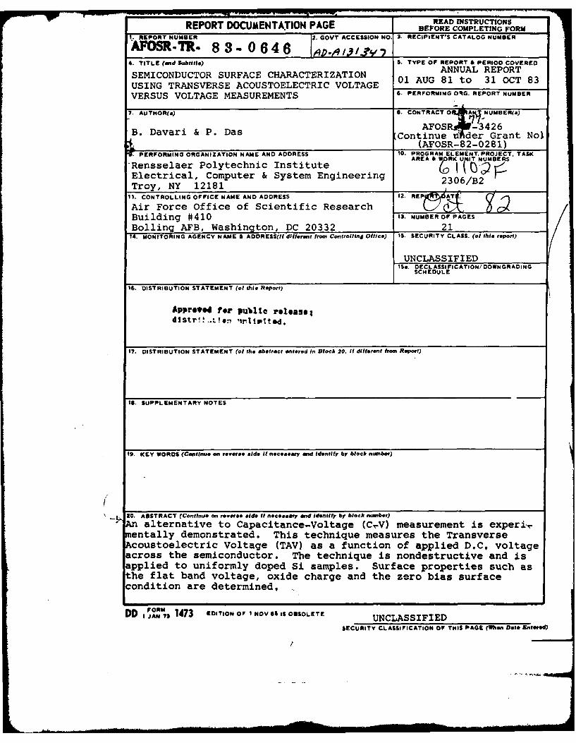
READ INSTRUCTIONSREPORT DOCUMENTATION PAGE BEFORE COMPLETING FORM
I.. REPORT NUMBER 2. GOVT ACCESSION NO. 3. RECIPIENT'S CATALOG NUMBER
AFOSR -. 8 3- 0 6 4 6 -__ __ __ __
4. TITLE (and Subtitle) S. TYPE OF REPORT & PERIOD COVERED
SEMICONDUCTOR SURFACE CHARACTERIZATION ANNUAL REPORT
USING TRANSVERSE ACOUSTOELECTRIC VOLTAGE 01 AUG 81 to 31 OCT 83
VERSUS VOLTAGE MEASUREMENTS 6. PERFORMING ORG. REPORT NUMBER
7. AUTHOR(q) A. CONTRACT 0 API NUMBER(s)
AFOSR -3426B. Davari & P. Das Continue ti der Grant No)(AFOSR-82-0281)
S. PERFORMING ORGANIZATION NAME AND ADDRESS 10. PROGRAM ELEMENT. PROJECT, TASKAREA • WOKUITNMERS
Rensselaer Polytechnic Institute A I BERS
Electrical, Computer & System Engineering 2306/B2
Troy, NY 1218111. CONTROLLING OFFICE NAME AND ADDRESS 12. REPr A,
Air Force Office of Scientific ResearchBuilding #410 13. NUMBER OF PAGES
Bolling AFB, Washington, DC 20332 214. MONITORING AGENCY NAME & ADDRESS(II different from Controlling Office) IS. SECURITY CLASS. (of this report)
UNCLASSIFIEDI5a. DECLASSI FICATION/ DOWNGRADING
SCHEDULE
IS. DISTRIBUTION STATEMENT (of this Report)
Appreted for public release-dlstr!.,. .!o- -Irlipited.
17. DISTRIBUTION STATEMENT (of the abstract mitered In Block 20, It different from Report)
IS. SUPPLEMENTARY NOTES
19. KEY WORDS (Continue on reverse side If neceseary and identify by block number)
20. ABSTRACT (Continue an reverse side If neceseery and identify by block number)
An alternative to Capacitance-Voltage (CrV) measurement is experi-mentally demonstrated. This technique measures the TransverseAcoustoelectric Voltage (TAV) as a function of applied D.C, voltageacross the semiconductor. The technique is nondestructive and isapplied to uniformly doped Si samples. Surface properties such asthe flat band voltage, oxide charge and the zero bias surfacecondition are determined,
DD FORM 1473 EDITION OF I NOV 65 IS OBSOLETE UNCLASSIFIEDSECURITY CLASSIFICATION OF THIS PAGE (len Date Enteted)

P,.An annual interim report is being accepterc as'the Final repor:for AFOSR-77-3426. The technical effort is being continued for oneyear under AFOSR-82-0281. The Final report for this continuationwill contain more overall detail and should be considered as thefinal report for the entire technical effort.
SECURITY CL ASSIVICATION OFP AOE(ften Data Ente)

ABSTRACT
A surface acoustic wave (SAW) device has been developed under
AFOSR Grant No. 77-3426 for use in the nondestructive determination of the
electronic properties of semiconductors. The properties that can be
determined by this technique include the bulk and surface conductivity,
the location in the energy gap of traps, surface states, and interface
states, trap emission and absorption times and storage times in the
depletion layer. This characterization of the semiconductor could be per-
formed at progressive stages of device fabrication thereby improving yield
by identifying faulty processing steps. Preliminary investigations have
been conducted on silicon, ion-implanted silicon, gallium arsenide, indium
arsenide, gallium phosphide and cadmium sulfide. These are well documented
by 20 papers and 14 meeting presentations as listed in the report. The
technique uses surface acoustic waves on a piezoelectric substrate. The
electric field associated with the SAW interacts with free carriers of a
semiconductor placed near the piezoelectric surface. The interaction gen-
erates detectable currents in the semiconductor and attenuates the SAW.
By observing these effects while varying external parameters such as tem-
perature, applied acoustic power, SAW frequency, semiconductor surface
irradiation and bias voltage, the desired information is obtained.
This report discusses the progress made in the last year.
AIR FORCE OFFrCE OF SCIIFC .NOTICE OF TMANS, ITTAL TO DTIC
This techn1 ). Im~ vs been rev ipw-d m,approved for 1ubt- release IAWA2 19-1,2.Distribution is ualimited.
MATMHW J. *ERgahie. "eehoala InformatIon DIyIg Ion

1. INTRODUCTION
The research being carried out under this grant is directed toward
the development of a technique for nondestructive determination of electrical
properties of semiconductors using surface acoustic waves.
Recent developments in the field of semiconductor devices demand highly
reliable material processing techniques. This, in turn, requires increased
sophistication in monitoring the properties of the semiconductor during
processing. For example, the diminishing size and increasing packing
density necessary for silicon VLSI circuits places great importance on
detection of impurities and defects in order to maintain high yield. As
a second example, consider the high speed GaAs devices which are approach-
ing the production stage. The high electron mobility in GaAs offers a sig-
nificant improvement in operational speed for digital signal processing
with anticipated clock rates of 10 GEz or more. Since GaAs is a direct
gap semiconductor, laser diodes can be fabricated on it opening the way to
single chip integration of signal processing and light source for optical
transmission systems. But before these devices can be reliably produced
with high yield, several material and processing obstacles must be over-
come. Some of these problems may not be best solved by the conventional
techniques employed for silicon.
It is projected that the use of the surface acoustic wave (SAW) tech-
nique can provide the energy location, concentration, capture and emission
rates, and spatial distribution of energy levels within the bandgap of
various semiconductors. Investigations have been performed on silicon,
gallium arsenide, gallium phosphide, indium arsenide and cadmium sulfide.
Because of the importance of GaAs, special emphasis is being given to
anodically oxidized GaAs. The SAW technique can also be effective in
[.
characterizing ion implanted semiconductors. Measurements can be performed
which will detect the presence of the ion implanted layer near the semicon-
ductor surface and its effective dose, lifetime, and conductivity. The
effectiveness of annealing also can be monitored nondestructively.
Semiconductor testing using surface acoustic waves has the unique
advantage of being contactless; there is no need to form a junction or apply
a metal to the surface. It is possible to test the same sample after each
processing step without disturbing the electrical or physical properties of
the sample.
Significant progress has been made in the development of this non-
destructive semiconductor evaluation technique using SAW in the last few
years. In the last reporting year significant results have been obtained
in the general area of contactless C-V measurements using SAW-semiconductor
interaction. This is discussed in papers nos. 18 and 19 listed in the next
section. As the papers 18, 19 and 20 are not yet published, they are
included in this report.
LIST OF PUBLICATIONS RESULTING FROM THIS AFOSR GRANT
1. P. Das, R. T. Webster, H. Estrada-Vazquez and W. C. Wang, "ContactlessSemiconductor Surface Characterization Using Surface Acoustic Waves",Surface Science 86, pp. 848-857, 1979.
2. R. T. Webster, H. Estrada-Vazquez, P. Das and R. Bharat, "Study of theSurface Properties of Thermally Oxidized Silicon Using Surface AcousticWave Attenuation", Solid State Electronics, Vol. 22, pp. 541-548, 1979.
3. P. Das, H. Estrada-Vazquez and R. Webster, "Transverse AcoustoelectricVoltage (TAV) Spectroscopy of High Resistivity GaAs", J. Appl. Phys.,Vol. 50, pp. 4942-4950, 1979.
4. R. Bharat, P. Das, R. T. Webster and H. Estrada-Vazquez, "ContactlessMeasurement of Carrier Generation Rate in Semiconductors", Proceedingsof the Topical Conference on Characterization Techniques for Semicon-ductor Materials and Science, pp. 93-105, 1978.

5. F. N. Mohammed Ayub and P. Das, "Spectroscopy of InAs Using SAW Gen-erated Transverse Acoustoelectric Voltage", J. Appl. Phys., Vol. 51,pp. 433-436, 1980.
6. P. Das, "Transverse Acoustoelectric Voltage (TAV) Spectroscopy ofGallium Phosphide, Indium Arsenide and Cadmium Sulphide-Nickel Chloride",J. Vac. Sc. and Tech., Vol. 16, pp. 1379-1382, 1979.
7. P. Das, M. K. Roy, R. T. Webster and K. Varahramyan, "NondestructiveEvaluation of Si Wafers Using SAW", 1979 Ultrasonics Symposium Proceed-ings, IEEE Publication No. 79 CH 1482-9, pp. 278-283, 1979.
8. K. Varahra.yan, R. T. Webster and P. Das, "Contactless Monitoring ofImpurity Activation in Ion-Implanted Silicon by Surface Acoustic WaveTechniques", J. Appl. Physics, Vol. 51, pp. 1234-1237, 1980.
9. P. Das, H. Gilboa, K. Varahramyan and R. T. Webster, "NondestructiveEvaluation of Semiconductor Surfaces Using the Surface Acoustic WaveConvolver", Proceedings of the 14th Electrical Electronics InsulationConference, IEEE Publication No. 79 CH 1510-7-El, pp. 284-289, 1979.
10. P. Das, R. T. Webster and B. Davari, "SAW Characterization of Photo-Voltaic Solar Cell", Electrochemical Society Extended Abstracts, Vol. 79-1,Spring Meeting, Boston, Ml%, May 6-11, 1979.
11. B. Davari and P. Das, "The Study of the Effect of Growth Parameters onthe Electrical Properties of the GaAs Oxide Layer Grown by Anodic Oxida-tion", Electrochemical Scoiety Extended Abstracts, Vol. 81-2, FallMeeting, Denver, CO, October 11-16, 1981.
12. P. Das, S. N. Chakravarti and K. N. Bhat, "Characteristics of GaAs-AnodicOxide Metal-Oxide-Semiconductor Solar Cells", J. Applied Phys., 52(3),1605-1607, 1981.
13. S. N. Chakravarti, P. Das, R. T. Webster and K. N. Bhat, "CW Argon LaserAnnealing of Anodic Oxide", J. Appl. Phys., 52(2), 1132-1133, 1981.
*14. B. Davari and P. Das, "A Study of the High Resistivity GaAs Surface andthe GaAs/oxide-Interface Using Two Beam Transverse Acousto-electricVoltage Speetroscopy", J. Appl. Phys. 3(5), May 1982, pp. 3668-3672.
*15. K. Varahramyan and P. Das, "Electrical Surface Properties of Semi-insul-ating and Ion-implanted GaAs Revealed by Thermo-optical Acousto-electricVoltage Method", Solid State Electronics, Vol. 25, No. 6, pp. 517-524, 1982.
*16. K. Varahramyan and P. Das, "Nondestructive Evaluation of GaAs by AEVMeasurements", 1981 Ultrasonics Symposium Proceedings, IEEE CatalogNo. 81-CH-1689-9, pp. 755-760, 1981.
*17. B. Davari and P. Des, "Quenching and Enhancement of the Exciton andSubbandgap Absorption in GaAs:CR Using the Two-beam Tranverse Acousto-electric Voltage Spectroscopy", Applied Physics Letters, 49(9) pp. 807-809,1982.
**18. B. Davari, P. Das and R. Bharat, "Semiconductor Surface Character-
ization Using Transverse Acoustoelectric Voltage Versus VoltageMeasurements", J. Appl. Physics, Jan. 1983, to be published.
**19. B. Davari and P. Des, "Profiling the Implanted Region in Si, UsingNondestructive Transverse Acoustoelectric Voltage vs. Voltage Tech-nique", Proceedings of the 1982 Ultrasonics Symposium, to be pub-lished.
**20. M. Tabib-Azar, B. Davari and P. Des, "Study of the Effect of AnodicOxidation on High Resistivity GaAs Surface States Using Two BeamAcoustoelectric Voltage Spectroscopy", to be published.
*Previously listed as to be published
**New papers in the last reporting period.
LIST OF PRESENTATIONS IN MEETING RESULTING FROM THIS AFOSR GRANT
1. P. Das, R. T. Webster, H. Estrada-Vazquez and W. C. Wang, "ContactlessSemiconductor Characterization using Surface Acoustic Waves", presentedat the International Conference on Solid Films and Surfaces, Tokyo,Japan, July 5-8, 1978.
2. P. Das, H. Estrada-Vazquez and R. T. Webster, "GaAs Surface SpectroscopyUsing Surface Acoustic Waves", American Physical Society March meeting,Washington, May 21-26, 1978.
3. R. Bharat, P. Das, R. T. Webster and H. Estrada-Vazquez, "ContactlessMeasurement of Carrier Generation Rate in Semiconductors", presentedat the 153rd Meeting of the Electrochemical Society, Seattle, Washington,May 21-26, 1978.
4. P. Das and R. T. Webster, "Transverse Acoustoelectric Voltage (TAV)Spectroscopy of Gallium Phosphide and Indium Arsenide", presented atthe American Physical Society Meeting, March 19-23, 1979, Chicago,Illinois.
5. R. Bharat and P. Das, "Nondestructive Monitoring of Impurity Activationin Ion-implanted Silicon by Surface Acoustic Waves", presented at theElectrochemical Society Meeting, May 6-11, 1979, Boston, Massachusetts.
6. P. Das, M. K. Roy, R. T. Webster and K. Varahramyan, "NondestructiveEvaluation of Si Wafers Using SAW", presented at the UltrasonicsSymposium, New Orleans, Sept. 26-28, 1979.
7. P. Das, H. Gilboa, K. Varahramyan and R. T. Webster, "NondestructiveEvaluation of Semiconductor Surfaces Using the Surface Acoustic WaveConvolver", presented at the 14th Electrical/Electronics InsulationConference, Boston, MA, October 8-11, 1979.

8. P. Das, "Transverse Acoustoelectric Voltage (TAV) Spectroscopy ofGallium Phosphide, Indium Arsenide and Cadmium Sulphide-Nickel Chloride",presented at the Conference on Physics of Compound Semiconductor inter-faces, Monterrey, California, Jan. 30-Feb. 2, 1979.
9. K. Varahramyan and P. Das, "Study of Electrical Activation in Ion-Implanted GaAs", presented at the American Physical Society Meeting,March 16-20, 1981.
10. B. Davari and P. Das, "The Effect of Growth Parameters on the Prop-erties of the GaAs Oxide Layer, Grown by Anodic Oxidation", presentedat the Electrochemical Society Meeting, Denver, Colorado, October 11-16,1981.
11. K. Varahramyan and P. Das, "Nondestructive Evaluation of GaAs by AEVMeasurements" presented at the IEEE Ultrasonics Symposium, Chicago,Illinois, October 14-16, 1981.
12. B. Davari and P. Das, "Evaluation of GaAs Interface States Using TwoBeam TAV Spectroscopy, presented at the APS March Meeting, Dallas, TX,March 8-12, 1982.
13. B. Davari and P. Das, "Profiling the Implanted Region in Si UsingNondestructive Transverse Acoustoelectric Voltage Versus VoltageTechnique", presented at the IEEE Ultrasonics Symposium, San Diego, CA,October 27-29, 1982.
14. M. Tabib-Azar, B. Davari and P. Das, "Study of the Effect of AnodicOxidation on High Resistivity GaAs Surface States Using Two BeamAcousto-Electric Voltage Spectroscopy", to be presented at the NewYork Meeting of APS, 24-27, Jan. 1983.

DA E
FILMED
tow
83
DTIC