RENICE X5 1.8 PATA ZIF SSD Data Sheet -...
20
1 Renice Technology Co., Limited 2013 Renice Technology Co., Limited 2013-12-25 RENICE X5 1.8” PATA ZIF SSD Data Sheet
Transcript of RENICE X5 1.8 PATA ZIF SSD Data Sheet -...

1 Renice Technology Co., Limited
2013
Renice Technology Co., Limited
2013-12-25
RENICE X5 1.8” PATA ZIF SSD Data Sheet

2 Renice Technology Co., Limited
CATALOGUE
1. Introduction ............................................................................. 3
1.1 Product Overview ........................................................................................... 3
1.2 Feature ........................................................................................................... 3
1.3 Functional Description .................................................................................... 4
2. Functional Block Diagram ...................................................... 5
3. Product Specifications ........................................................... 6
3.1 Physical Specifications ................................................................................... 6
3.2 Host Interface ................................................................................................. 6
3.3 FPC Description (unit: mm) ............................................................................ 7
4. Interface Description .............................................................. 8
4.1 Pin Assignment .............................................................................................. 8
4.2 Pin Description ............................................................................................... 8
5. Electric Specifications ............................................................ 9
5.1 Power Specification ........................................................................................ 9
5.2 Power Supply Voltage .................................................................................... 9
5.3 SSD Power Consumption (typical) ................................................................. 9
6. Reliability Specification .........................................................10
6.1 Wear-leveling ............................................................................................... 10
6.2 Endurance .................................................................................................... 10
6.3 H/W ECC and EDC for NAND Flash ............................................................ 10
6.4 MTBF ........................................................................................................... 10
7 Software Interface ................................................................... 11
7.1 Command Set .............................................................................................. 11
7.2 SMART Feature Set ..................................................................................... 12
7.2.1SMART Data Structure ........................................................................ 13
7.2.2 SMART Attributes ............................................................................... 14
7.3 Identify Device ............................................................................................. 14
8. Buy Information .....................................................................19
9. Product Part Number Naming Rule ......................................20

3 Renice Technology Co., Limited
1. Introduction
1.1 Product Overview
RENICE X5 Series 1.8” PATA ZIF SSD offers ultra high performance and extreme low power
consumption. It supports DMA mode up to UDMA 7, and is equipped with powerful Error
Correction Coding (ECC) to support NAND Flash with more stability. Meanwhile, advanced
technology to transfer data to the host via a high efficiency DMA engine and utilizes the internal
memory buffer in a sufficient way significantly improve X5’s performance. Generally, based on
optimized wear leveling, bad block management and flash management technologies, X5 ZIF
SSD delivers extraordinary performance in data read/write speed and keeps data more reliable for
industrial PATA interface applications.
1.2 Feature
● Performance:
Read: 117MB/s Write: 110MB/s (@128GB MLC)
● Form factor: 1.8-inch (71.0mm x 54.0mm x 5.2mm) L×W×H
● Interface standard: 40Pin PATA ZIF
● Density: 8GB, 16GB, 32GB, 64GB, 128GB, 256GB
● Input voltage: 3.3V (±5%)
● Commercial operating temperature range from 0℃ to +70℃
Industrial operating temperature range from -40℃ to +85℃
● Flash management algorithm: static and dynamic wear-leveling, bad block management
algorithm.
● Supports dynamic power management and SMART (Self-Monitoring, Analysis and Reporting
Technology).
● SSD controller core internal detectors for power fail protection.
● Hardware BCH ECC capable of correcting errors up to 72-bit/1KB
● Write endurance: >8 years @ 100GB write/day ( 32GB SLC SSD)
● Read endurance: unlimited
● Data retention: JESD47 compliant
● MTBF: 3,000,000 Hours

4 Renice Technology Co., Limited
1.3 Functional Description
Host Interface
Compliant with ATA-8 specifications, RENICE X5 1.8” ZIF SSD’s PATA interface supports data
transfer modes PIO 0 to 6, Multiword DMA modes 0 to 4, and Ultra DMA modes up to UMDA 7.
Also, X5 supports the PCMCIA UDMA mode, which is supported by new generation of Digital
Single Lens Reflex (DSLR) cameras. X5 can be operated at 5V or 3.3V power supply with output
voltage automatically adjusted. With built-in voltage regulator, only 1 single power supply is
required for the core logic and flash.
Flash Interface and Data Transfer
In addition to support of quad channel access, the flash interface enables two-way or four-way
interleaving for a multi-bank NAND flash connection to obtain optimal performance. RENICE X5
can connect up to 16 NAND devices (4 chip-enable pins per channel) and be used in high
capacity flash disk drives.
RENICE X5 uses a superior DMA technology to transfer data between the host and NAND flash
interface. The DMA technology transfers data at a very high rate in both directions (read and write)
and by doing so, effectively decreases microprocessor loading.
ECC
With multi-mode correction capability up to 72 bits/1K, the powerful Error Correction Coding (ECC)
engine supports almost all kinds of NAND Flash. The hardware ECC engine executes parity
generation and error detection/correction features, and enhances decoding throughput and data
reliability.
SMART Command
Renice X5 1.8 ZIF SSD provides SMART command support that allows users to read spare and
bad block information. Users can thus evaluate drive health at run time and receive an early
warning before the flash drive lifespan ends.

5 Renice Technology Co., Limited
2. Functional Block Diagram
Figure 1: Block Diagram

6 Renice Technology Co., Limited
3. Product Specifications
3.1 Physical Specifications
Form factor 1.8 inch
Dimensions(mm)
Length 71.00±0.40
Width 54.00±0.20
Height 5.20±0.15
Weight <40g
Connector 40pin PATA ZIF FFC connector
3.2 Host Interface
− Compliant with ATA/ATAPI-8
− Supports PIO Mode 0 - 6
− Supports Multiword DMA Mode 0 - 4
− Supports Ultra DMA Mode 0 - 7
− Supports PCMCIA Extended Memory Mode (cycle time: 250, 120, 100, 80 ns)
− Supports PCMCIA Ultra DMA Mode 0 - 7

7 Renice Technology Co., Limited
3.3 FPC Description (unit: mm)

8 Renice Technology Co., Limited
4. Interface Description
4.1 Pin Assignment
4.2 Pin Description
Pin No Pin Name Pin No Pin Name Pin No Pin Name Pin No Pin Name
1 RSV1 11 DD4 21 GND2 31 DA1
2 RSV2 12 DD11 22 DMARQ 32 PDIAG
3 RESET 13 DD3 23 GND3 33 DA0
4 GND1 14 DD12 24 DIOW 34 DA2
5 DD7 15 DD2 25 DIOR 35 CS0
6 DD8 16 DD13 26 GND4 36 CS1
7 DD6 17 DD1 27 IORDY 37 DASP
8 DD9 18 DD14 28 GND5 38 3.3V1
9 DD5 19 DD0 29 DMACK 39 3.3V2
10 DD10 20 DD15 30 INTRQ 40 RSV3
9 Renice Technology Co., Limited
5. Electric Specifications
5.1 Power Specification
Operating voltage: 3.3V (±5%)
5.2 Power Supply Voltage
1.8V for Core, 3.3V for NAND,
5.3 SSD Power Consumption (typical)
Operation (Read/Write) – 1.65W @256GB MLC
Idle – 0.3W
Standby – 0.3W
Sleep (Partial/Slumber) – 0.2W/0.06W
10 Renice Technology Co., Limited
6. Reliability Specification
Item Features
Temperature Operating Commercial:0~+70℃
Industrial:-40~+85℃
Humidity 5-95%
Vibration 20G(7-2000HZ)
Shock 2,000G(@0.3ms half sine wave)
6.1 Wear-leveling
Renice X5 SSD support both static and dynamic wear-leveling. These two algorithms
guarantee all type of flash memory at same level of erase cycles to improve lifetime
limitation of NAND based storage.
6.2 Endurance
Write endurance: >8 years @ 100GB write/ day (30GB)
Read endurance: unlimited
6.3 H/W ECC and EDC for NAND Flash
Hardware BCH ECC capable of correcting errors up to 72-bit/1KB
6.4 MTBF
MTBF(Mean Time between Failures) of Renice X5 1.8” ZIF SSD:>3,000,000 hours
Data retention: JESD47 compliant

11 Renice Technology Co., Limited
7 Software Interface
7.1 Command Set
Command Set Command Command Code Protocol
General Feature Set
Execute Drive Diagnostic 90h Device diagnostic
Flush Cache E7h Non-data
Identify Device ECh PIO data-in
Read DMA C8h DMA
Read Multiple C4h PIO data-in
Read Sector(s) 20h or 21h PIO data-in
Read Verify Sector(s) 40h or 41h Non-data
Set Feature EFh Non-data
Set Multiple Mode C6h Non-data
Write DMA CAh DMA
Write Multiple C5h PIO data-out
Write Sector(s) 30h or 31h PIO data-out
NOP 00h Non-data
Read Buffer E4h PIO data-in
Write Buffer E8h PIO data-out
Set Feature EFh Non-data
Power Management
Feature Set
Check Power Mode E5h or 98h Non-data
Idle E3h or 97h Non-data
Idle Immediate E1h or 95h Non-data
Sleep E6h or 99h Non-data
Standby E2h or 96h Non-data
Standby Immediate E0h or 94h Non-data
Security Mode
Feature Set
Security Set Password F1h PIO data-out
Security Unlock F2h PIO data-out
Security Erase Prepare F3h Non-data
Security Erase Unit F4h PIO data-out
Security Freeze Lock F5h Non-data
Security Disable Password F6h PIO data-out
SMART Feature Set
SMART Disable Operations B0h Non-data
SMART Enable/Disable
Autosave B0h Non-data
SMART Enable Operations B0h Non-data
SMART Return Status B0h Non-data

12 Renice Technology Co., Limited
SMART Feature Set
SMART Execute Off-Line
Immediate B0h Non-data
SMART Read Data B0h PIO data-in
SMART Read Threshold B0h PIO data-in
SMART Save Attribute Value B0h Non-data
Host Protected Area
Feature Set
Read Native Max Address F8h Non-data
Set Max Address F9h Non-data
Set Max Set Password F9h PIO data-out
Set Max Lock F9h Non-data
Set Max Freeze Lock F9h Non-data
Set Max Unlock F9h PIO data-out
48-bit Address
Feature Set
Read Sector Ext 24h PIO data-in
Read DMA Ext 25h DMA
Read Multiple Ext 29h PIO data-In
Write Sector Ext 34h PIO data-out
Write DMA Ext 35h DMA
Write Multiple Ext 39h PIO data-out
Write DMA FUA Ext 3Dh DMA
Read Verify Sector Ext 42h Non-data
Write Multiple FUA Ext CEh PIO data-out
Flush Cache Ext EAh Non-data
Others
Format Track 50h PIO data-out
Initialize Drive Parameters 91h Non-data
Recalibrate 1Xh Non-data
Seek 7Xh Non-data
Wear Level F5h Non-data
Write Verify 3Ch PIO data-out
7.2 SMART Feature Set
Renice X5 1.8 ZIF SSD supports the SMART (Self-Monitoring, Analysis and Reporting Technology) command set and defines some vendor-specific data to report spare/bad block numbers in each memory management unit.
Value Command Value Command
D0h Read Data D5h Reserved
D1h Read Attribute Threshold D6h Reserved
D2h Enable/Disable Autosave D8h Enable SMART Operations
D3h Save Attribute Values D9h Disable SMART Operations
D4h Execute OFF-LINE Immediate DAh Return Status

13 Renice Technology Co., Limited
If the reserved size is below the threshold, the status can be read from the Cylinder Register using the Return Status command (DAh).
7.2.1SMART Data Structure
The following 512 bytes make up the device SMART data structure. Users can obtain the data using the “Read Data” command (D0h).
Byte F / V Description
0 - 1 X Revision code
2 - 361 X Vendor specific (see 4.2.2)
362 V Off-line data collection status
363 X Self-test execution status byte
364 - 365 V Total time in seconds to complete off-line data collection activity
366 X Vendor specific
367 F Off-line data collection capability
368 - 369 F SMART capability
370 F
Error logging capability
• 7-1 Reserved
• 0-1 = Device error logging supported
371 X Vendor specific
372 F Short self-test routine recommended polling time (in minutes)
373 F Extended self-test routine recommended polling time (in minutes)
374 F Conveyance self-test routine recommended polling time (in minutes)
375 - 385 R Reserved
386 - 395 F Firmware Version/Date Code
396 - 399 R Reserved
400 - 406 F Chips Information
407 - 511 R Reserved
Notes:
1. F = content (byte) is fixed and does not change.
2. V = content (byte) is variable and may change depending on the state of the device or
the commands executed by the device.
3. X = content (byte) is vendor specific and may be fixed or variable.
4. R = content (byte) is reserved and shall be zero.

14 Renice Technology Co., Limited
7.2.2 SMART Attributes
The following table defines the vendor specific data in byte 2 to 361 of the 512-byte SMART data.
Attribute
ID (hex) Raw Attribute Value Attribute Name
01 LSB MSB 00 00 00 00 Read error rate
05 LSB MSB 00 00 00 00 Reallocated sector count
0C LSB MSB 00 00 00 00 Power cycle count
A1 LSB MSB 00 00 00 00 Number of valid spare block
A2 LSB MSB 00 00 00 00 Number of child pair
A3 LSB MSB 00 00 00 00 Number of initial invalid block
A4 LSB MSB 00 00 Number of total erase count
A5 LSB MSB 00 00 Maximum erase count
A6 LSB MSB 00 00 Minimum erase count
A7 LSB MSB 00 00 Average erase count
C0 LSB MSB 00 00 Power-off retract count
C7 LSB MSB 00 00 00 00 UDMA CRC error count
F1 LSB MSB Total LBAs written (each write unit = 32MB)
F7 LSB MSB Total LBAs read (each read unit = 32MB)
7.3 Identify Device
The Identify Device command enables the host to receive parameter information from the Renice X5. This command has the same protocol as the Read Sector(s) command. The parameter words in the buffer have the arrangement and meanings defined in the following.
ID Table Information in PCMCIA Mode
Word Address
Default
Value
Total
Bytes Data Field Type Information
0 848Ah 2 General configuration - signature for the Compact Flash Storage
Card
1 XXXXh 2 Default number of cylinders
2 0000h 2 Reserved
3 00XXh 2 Default number of heads
4 0000h 2 Obsolete
5 0240h 2 Obsolete
6 XXXXh 2 Default number of sectors per track
7-8 XXXXh 4 Number of sectors per card (Word 7 = MSW, Word 8 = LSW)
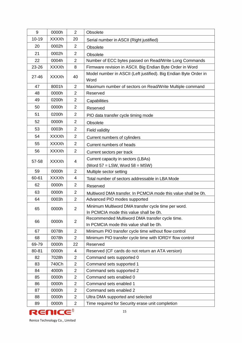
15 Renice Technology Co., Limited
9 0000h 2 Obsolete
10-19 XXXXh 20 Serial number in ASCII (Right justified)
20 0002h 2 Obsolete
21 0002h 2 Obsolete
22 0004h 2 Number of ECC bytes passed on Read/Write Long Commands
23-26 XXXXh 8 Firmware revision in ASCII. Big Endian Byte Order in Word
27-46 XXXXh 40 Model number in ASCII (Left justified). Big Endian Byte Order in
Word
47 8001h 2 Maximum number of sectors on Read/Write Multiple command
48 0000h 2 Reserved
49 0200h 2 Capabilities
50 0000h 2 Reserved
51 0200h 2 PIO data transfer cycle timing mode
52 0000h 2 Obsolete
53 0003h 2 Field validity
54 XXXXh 2 Current numbers of cylinders
55 XXXXh 2 Current numbers of heads
56 XXXXh 2 Current sectors per track
57-58 XXXXh 4 Current capacity in sectors (LBAs)
(Word 57 = LSW, Word 58 = MSW)
59 0000h 2 Multiple sector setting
60-61 XXXXh 4 Total number of sectors addressable in LBA Mode
62 0000h 2 Reserved
63 0000h 2 Multiword DMA transfer. In PCMCIA mode this value shall be 0h.
64 0003h 2 Advanced PIO modes supported
65 0000h 2 Minimum Multiword DMA transfer cycle time per word.
ln PCMCIA mode this value shall be 0h.
66 0000h 2 Recommended Multiword DMA transfer cycle time.
In PCMCIA mode this value shall be 0h.
67 0078h 2 Minimum PIO transfer cycle time without flow control
68 0078h 2 Minimum PIO transfer cycle time with lORDY flow control
69-79 0000h 22 Reserved
80-81 0000h 4 Reserved (CF cards do not return an ATA version)
82 7028h 2 Command sets supported 0
83 740Ch 2 Command sets supported 1
84 4000h 2 Command sets supported 2
85 0000h 2 Command sets enabled 0
86 0000h 2 Command sets enabled 1
87 0000h 2 Command sets enabled 2
88 0000h 2 Ultra DMA supported and selected
89 0000h 2 Time required for Security erase unit completion

16 Renice Technology Co., Limited
90 0000h 2 Time required for Enhanced security erase unit completion
91 0000h 2 Current Advanced power management value
92 0000h 2 Reserved
93-99 0000h 14 Reserved
100-103 XXXXh 8 Maximum user LBA for the 48-bit Address feature set
104-127 0000h 48 Reserved
128 0000h 2 Security status
129-159 0000h 62 Vendor unique bytes
160 81F4h 2 Power requirement description
161 0000h 2 Reserved
162 0000h 2 Key management schemes supported
163 0000h 2 CF Advanced True lDE Timing Mode Capability and Setting
164 8FDBh 2 CF Advanced PCMCIA I/O and Memory Timing Mode Capability
and Setting
165-166 0000h 4 Reserved
167 6002h 2 CFA Revision and Enhanced Features Support
168-175 0000h 16 Reserved
176-255 0000h 160 Reserved
ID Table Information in PATA Mode
Word Address
Default
Value
Total
Bytes Data Field Type Information
0 044Ah 2 General configuration
1 XXXXh 2 Default number of cylinders
2 0000h 2 Reserved
3 00XXh 2 Default number of heads
4 0000h 2 Obsolete
5 0240h 2 Obsolete
6 XXXXh 2 Default number of sectors per track
7-8 XXXXh 4 Number of sectors per card (Word 7 = MSW, Word 8 = LSW)
9 0000h 2 Obsolete
10-19 XXXXh 20 Serial number in ASCII (Right justified)
20 0002h 2 Obsolete
21 0002h 2 Obsolete
22 0004h 2 Obsolete
23-26 XXXXh 8 Firmware revision in ASCII. Big Endian Byte Order in Word
27-46 XXXXh 40 Model number in ASCII (Left justified). Big Endian Byte Order in
Word
47 8001h 2 Maximum number of sectors on Read/Write Multiple command
48 0000h 2 Reserved
49 0F00h 2 Capabilities

17 Renice Technology Co., Limited
50 4000h 2 Capabilities
51 0200h 2 PIO data transfer cycle timing mode
52 0000h 2 Obsolete
53 0007h 2 Field validity
54 XXXXh 2 Current numbers of cylinders
55 XXXXh 2 Current numbers of heads
56 XXXXh 2 Current sectors per track
57-58 XXXXh 4 Current capacity in sectors (LBAs)
(Word 57 = LSW, Word 58 = MSW)
59 0000h 2 Multiple sector setting
60-61 XXXXh 4 Total number of sectors addressable in LBA Mode
62 0000h 2 Reserved
63 0007h 2 Multiword DMA transfer. In PCMCIA mode this value shall be 0h.
64 0003h 2 Advanced PIO modes supported
65 0078h 2 Minimum Multiword DMA transfer cycle time per word.
ln PCMCIA mode this value shall be 0h.
66 0078h 2 Recommended Multiword DMA transfer cycle time.
In PCMCIA mode this value shall be 0h.
67 0078h 2 Minimum PIO transfer cycle time without flow control
68 0078h 2 Minimum PIO transfer cycle time with lORDY flow control
69-79 0000h 22 Reserved
80 03FCh 2 Major version number (ATA8-ACS2)
81 0000h 2 Minor version number
82 7028h 2 Command sets supported 0
83 7500h 2 Command sets supported 1
84 4000h 2 Command sets supported 2
85 0000h 2 Command sets enabled 0
86 0000h 2 Command sets enabled 1
87 0000h 2 Command sets enabled 2
88 007Fh 2 Ultra DMA mode supported and selected
89 0000h 2 Time required for Security erase unit completion
90 0000h 2 Time required for Enhanced security erase unit completion
91 0000h 2 Current Advanced power management value
92 0000h 2 Master Password revision code
93
604Fh
6F00h
603Fh
2
. Hardware reset result (Master)
. Hardware reset result (Slave)
. Hardware reset result (Master w/ slave present)
94-99 0000h 12 Reserved
100-103 XXXXh 8 Maximum user LBA for the 48-bit Address feature set
104-127 0000h 48 Reserved
128 0000h 2 Security status

18 Renice Technology Co., Limited
129-159 0000h 62 Vendor unique bytes
160 0000h 2 Power requirement description
161 0000h 2 Reserved
162 0000h 2 Key management schemes supported
163 0000h 2 CF Advanced True lDE Timing Mode Capability and Setting
164 0000h 2
. CF Advanced PCMCIA I/O and Memory Timing Mode Capability
and Setting
. 80 ns cycle in memory and I/O mode
165-175 0000h 22 Reserved
176-255 0000h 160 Reserved
19 Renice Technology Co., Limited
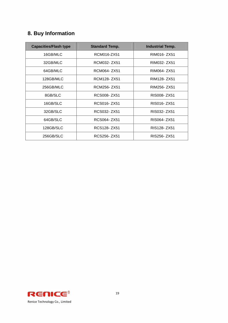
8. Buy Information
Capacities/Flash type Standard Temp. Industrial Temp.
16GB/MLC RCM016-ZX51 RIM016- ZX51
32GB/MLC RCM032- ZX51 RIM032- ZX51
64GB/MLC RCM064- ZX51 RIM064- ZX51
128GB/MLC RCM128- ZX51 RIM128- ZX51
256GB/MLC RCM256- ZX51 RIM256- ZX51
8GB/SLC RCS008- ZX51 RIS008- ZX51
16GB/SLC RCS016- ZX51 RIS016- ZX51
32GB/SLC RCS032- ZX51 RIS032- ZX51
64GB/SLC RCS064- ZX51 RIS064- ZX51
128GB/SLC RCS128- ZX51 RIS128- ZX51
256GB/SLC RCS256- ZX51 RIS256- ZX51

20 Renice Technology Co., Limited
9. Product Part Number Naming Rule