Renesas Synergy™ Software Package (SSP) v1.1.0 … · RFC 793 Transmission Control Protocol (TCP)...
78
R01DS0272EU0111 Rev.1.11 Page 1 of 77 Jun 1, 2016 Datasheet Renesas Synergy™ Software Package (SSP) SSP Version 1.1.0 1. Description The Renesas Synergy TM Software Package (SSP), the heart of the Renesas Synergy TM Platform, is a complete integrated software package that was created using industry best practices and tested to commercial standards. It is composed of a real- time operating system (RTOS), middleware, communication stacks, function libraries, a rich application framework, and low-level drivers. The major components of the SSP include Express Logic’s X-Ware™. X-Ware includes the premier ThreadX ® RTOS plus middleware and stacks including NetX™ IPv4 and NetX Duo™ IPv4/IPv6 compliant TCP/IP stacks respectively, USBX™ USB Host/Device protocol stack, FileX ® MS-DOS compatible file system, and GUIX™ graphics runtime library. These are bundled in the Renesas SSP with additional libraries, a rich Application Framework, plus Hardware Abstraction Layer (HAL) drivers and Board Support Packages (BSP) that are completely optimized for use with Renesas Synergy Microcontrollers (MCU) and developed according to the IEC/ISO/IEEE-12207 Software Life Cycle Process standard while using the MISRA C:2012 coding guidelines. The SSP is supported and maintained by Renesas on a continuous basis, and Renesas warrants the SSP to operate as per the Performance section of this datasheet. Figure 1 Renesas Synergy™ Software Package R01DS0272EU0111 Rev.1.11 June 1, 2016
Transcript of Renesas Synergy™ Software Package (SSP) v1.1.0 … · RFC 793 Transmission Control Protocol (TCP)...

R01DS0272EU0111 Rev.1.11 Page 1 of 77 Jun 1, 2016
Datasheet
Renesas Synergy™ Software Package (SSP)
SSP Version 1.1.0
1. Description
The Renesas SynergyTM Software Package (SSP), the heart of the Renesas SynergyTM Platform, is a complete integrated
software package that was created using industry best practices and tested to commercial standards. It is composed of a real-
time operating system (RTOS), middleware, communication stacks, function libraries, a rich application framework, and
low-level drivers.
The major components of the SSP include Express Logic’s X-Ware™. X-Ware includes the premier ThreadX® RTOS plus
middleware and stacks including NetX™ IPv4 and NetX Duo™ IPv4/IPv6 compliant TCP/IP stacks respectively, USBX™
USB Host/Device protocol stack, FileX® MS-DOS compatible file system, and GUIX™ graphics runtime library. These are
bundled in the Renesas SSP with additional libraries, a rich Application Framework, plus Hardware Abstraction Layer
(HAL) drivers and Board Support Packages (BSP) that are completely optimized for use with Renesas Synergy
Microcontrollers (MCU) and developed according to the IEC/ISO/IEEE-12207 Software Life Cycle Process standard while
using the MISRA C:2012 coding guidelines. The SSP is supported and maintained by Renesas on a continuous basis, and
Renesas warrants the SSP to operate as per the Performance section of this datasheet.
Figure 1 Renesas Synergy™ Software Package
R01DS0272EU0111
Rev.1.11
June 1, 2016
Renesas Synergy™ Software Package (SSP) Datasheet
R01DS0272EU0111 Rev.1.11 Page 2 of 77 June 1, 2016
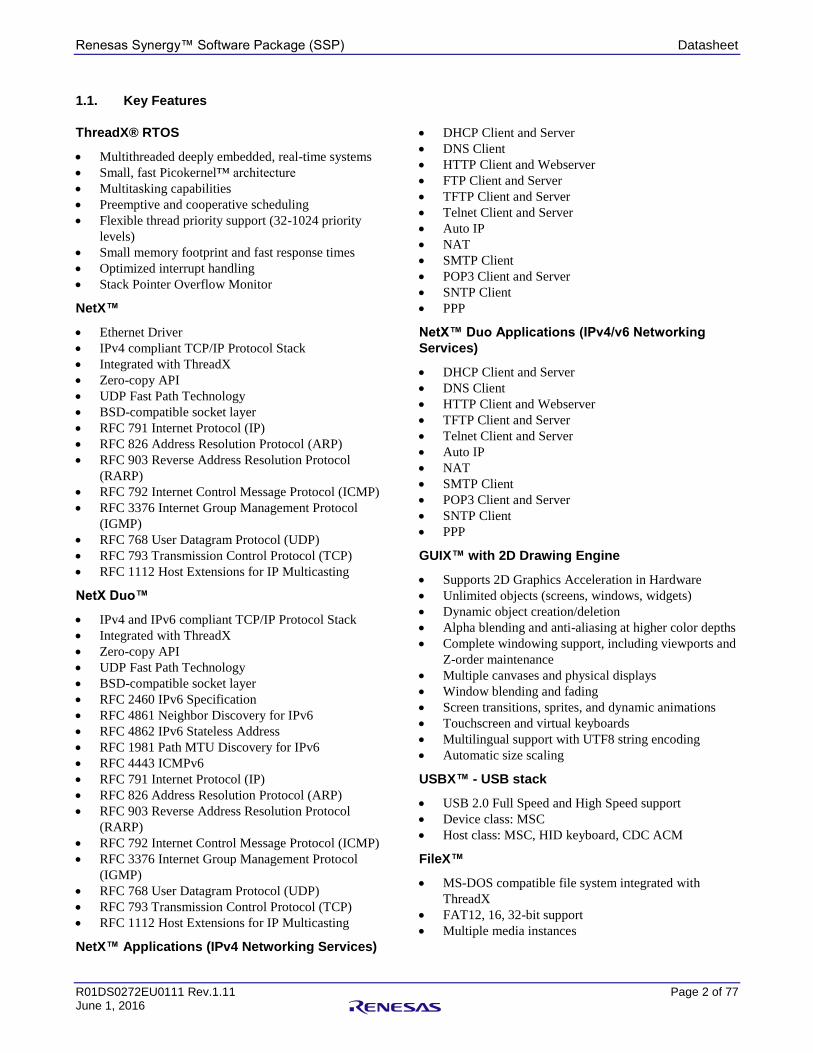
1.1. Key Features
ThreadX® RTOS
Multithreaded deeply embedded, real-time systems
Small, fast Picokernel™ architecture
Multitasking capabilities
Preemptive and cooperative scheduling
Flexible thread priority support (32-1024 priority
levels)
Small memory footprint and fast response times
Optimized interrupt handling
Stack Pointer Overflow Monitor
NetX™
Ethernet Driver
IPv4 compliant TCP/IP Protocol Stack
Integrated with ThreadX
Zero-copy API
UDP Fast Path Technology
BSD-compatible socket layer
RFC 791 Internet Protocol (IP)
RFC 826 Address Resolution Protocol (ARP)
RFC 903 Reverse Address Resolution Protocol
(RARP)
RFC 792 Internet Control Message Protocol (ICMP)
RFC 3376 Internet Group Management Protocol
(IGMP)
RFC 768 User Datagram Protocol (UDP)
RFC 793 Transmission Control Protocol (TCP)
RFC 1112 Host Extensions for IP Multicasting
NetX Duo™
IPv4 and IPv6 compliant TCP/IP Protocol Stack
Integrated with ThreadX
Zero-copy API
UDP Fast Path Technology
BSD-compatible socket layer
RFC 2460 IPv6 Specification
RFC 4861 Neighbor Discovery for IPv6
RFC 4862 IPv6 Stateless Address
RFC 1981 Path MTU Discovery for IPv6
RFC 4443 ICMPv6
RFC 791 Internet Protocol (IP)
RFC 826 Address Resolution Protocol (ARP)
RFC 903 Reverse Address Resolution Protocol
(RARP)
RFC 792 Internet Control Message Protocol (ICMP)
RFC 3376 Internet Group Management Protocol
(IGMP)
RFC 768 User Datagram Protocol (UDP)
RFC 793 Transmission Control Protocol (TCP)
RFC 1112 Host Extensions for IP Multicasting
NetX™ Applications (IPv4 Networking Services)
DHCP Client and Server
DNS Client
HTTP Client and Webserver
FTP Client and Server
TFTP Client and Server
Telnet Client and Server
Auto IP
NAT
SMTP Client
POP3 Client and Server
SNTP Client
PPP
NetX™ Duo Applications (IPv4/v6 Networking
Services)
DHCP Client and Server
DNS Client
HTTP Client and Webserver
TFTP Client and Server
Telnet Client and Server
Auto IP
NAT
SMTP Client
POP3 Client and Server
SNTP Client
PPP
GUIX™ with 2D Drawing Engine
Supports 2D Graphics Acceleration in Hardware
Unlimited objects (screens, windows, widgets)
Dynamic object creation/deletion
Alpha blending and anti-aliasing at higher color depths
Complete windowing support, including viewports and
Z-order maintenance
Multiple canvases and physical displays
Window blending and fading
Screen transitions, sprites, and dynamic animations
Touchscreen and virtual keyboards
Multilingual support with UTF8 string encoding
Automatic size scaling
USBX™ - USB stack
USB 2.0 Full Speed and High Speed support
Device class: MSC
Host class: MSC, HID keyboard, CDC ACM
FileX™
MS-DOS compatible file system integrated with
ThreadX
FAT12, 16, 32-bit support
Multiple media instances

Renesas Synergy™ Software Package (SSP) Datasheet
R01DS0272EU0111 Rev.1.11 Page 3 of 77 June 1, 2016
Memory support
Flash programming support via JTAG
Code and Data Flash drivers
External memory bus support
Human Machine Interface (HMI)
Graphics LCD controller driver
Segment LCD controller driver
Application Framework
Periodic Sampling ADC framework
Audio Playback framework
Audio Playback HW DAC framework
Audio Playback HW I2S framework
Capacitive Touch Sensing Unit framework
Capacitive Touch Sensing Unit Button framework
Capacitive Touch Sensing Unit Slider framework
Console framework
External Interrupt framework
I2C framework
Inter-Thread Messaging framework
JPEG Decode framework
Power Mode Profile framework
Synergy FileX Interface framework
Synergy GUIX Interface framework
Synergy NetX Communication framework
Synergy USBX Communication framework
Thread Monitor framework
Touch Panel I2C framework
UART framework
SPI Framework
Block Media Interface for SD Multi Media Card
Security Cryptographic Library
True RNG (TRNG)
SHA1, SHA224/SHA256
AES 128, 192, and 256-bits
3DES, 192-bit key
ARC4
RSA up to 2048-bit keys
DLP, DSA up to 2048-bit keys
CMSIS DSP Library
Basic math functions
Fast math functions
Complex math functions
Filters
Convolution
Matrix functions
Transforms
Motor control functions
Statistical functions
Support functions
Interpolation functions
Hardware Abstract Layer (HAL) Driver Modules
Clock Generation Circuit (CGC)
Capacitive Touch Sensing Unit (CTSU)
Digital to Analog converter (DAC)
Asynchronous General Purpose Timer (AGT)
Cyclic Redundancy Check calculator (CRC)
Clock Frequency Accuracy Measurement (CAC)
I2IC (RIIC)
Serial Peripheral Interface (SPI)
Quad SPI (QSPI)
Real Time clock (RTC)
Segment LCD (SLCD)
Serial Communication Interface UART (SCI_UART)
Serial Communication Interface I2C (SCI_I2C)
Serial Communication Interface SPI (SCI_SPI)
JPEG Codec
Flash Memory-High Performance (FLASH_HP)
Flash Memory-Low Power (FLASH_LP)
Data Transfer Controller (DTC)
SD Multi Media Card (SDMMC)
Data Operation Circuit (DOC)
Direct Memory Access Controller (DMAC)
Interrupt Controller Unit (ICU)
Event Link Controller (ELC)
General Purpose Timer (GPT)
General Purpose I/O Port (GPIO / IOPORT)
Keyboard Interrupt Interface (KINT)
Graphics LCD Controller (GLCD)
Watchdog Timer (WDT)
Independent Watchdog Timer (IWDT)
Analog to Digital Converter (ADC) (12-bit, 14-bit)
Factory Microcontroller Information (FMI)
Low Power Mode (LPM)
Controller Area Network Interface (CAN)
Serial Sound Interface (SSI)
Parallel Data Capture Unit (PDC)
Low Voltage Detection (LVD)
General PWM Timer with Input Capture
(GPT_INPUT_CAPTURE )
System and Power Management
Clock Frequency Accuracy Measurement Circuit
(CAC)
Low Power Modes driver
Power Profiles
RTC driver with calendar support
Event Link Controller (ELC)
DMA Controller (DMAC)
Data Transfer Controller (DTC)
Clock Generation and Management
GPIO
Unique ID
Stack Pointer Overflow Monitor

Renesas Synergy™ Software Package (SSP) Datasheet
R01DS0272EU0111 Rev.1.11 Page 4 of 77 June 1, 2016
Messaging Configurator
GPIO and Key Interrupts
GPIO module
Key Interrupts module
Board Support Package (BSP)
Supports S3, S7 and S1 series MCUs
Supports PE-HMI1, DK-S7G2, DK-S3A7, DK-S124
and SK-S7G2 Kits
Creation of custom BSPs using e2 studio
System initialization and configuration during startup
Software and hardware access control
Register Write Protection
1.2. Introduction
This SSP datasheet includes functional descriptions and specifies performance data for the major software modules that are
included in the Synergy Software Package (SSP).
Information prior to Section 15 of this datasheet provides a functional summary overview of each SSP software module,
including the memory footprint of each module for code (Flash memory) and data (SRAM). For a full description and
details of each SSP software module, please refer to the SSP User’s Manual.
Information in Section 15 in this datasheet includes SSP performance measurements of SSP software modules that may
include direct performance of individual software modules and in some cases the combined performance of several software
modules in higher system-level test scenarios.
The estimated memory requirements in this document specify the estimated memory consumption for each module. The
requirements are as follows:
Compiler: GCC 4.9 (Option: -O2)
Compiler: IAR 7.2 Embedded Workbench for Renesas SynergyOption: -Oh)
The memory usage for the modules includes:
Flash Memory Usage = .text + .data
SRAM Memory Usage = .data + .bss +.noinit
All performance tests in this document are included in section SSP System Performance – Warranted and Non-Warranted
and were conducted and measured on specific Synergy hardware systems, typically a Synergy Development Kit. This
section also specifies the test environment for each performance test that includes:
SSP version.
Renesas Synergy hardware (Development Kit).
When the Synergy hardware is specific, it also identifies which Synergy MCU is used, the operating frequency,
and the MCU configuration settings.
Toolchain version (including complier optimization levels).
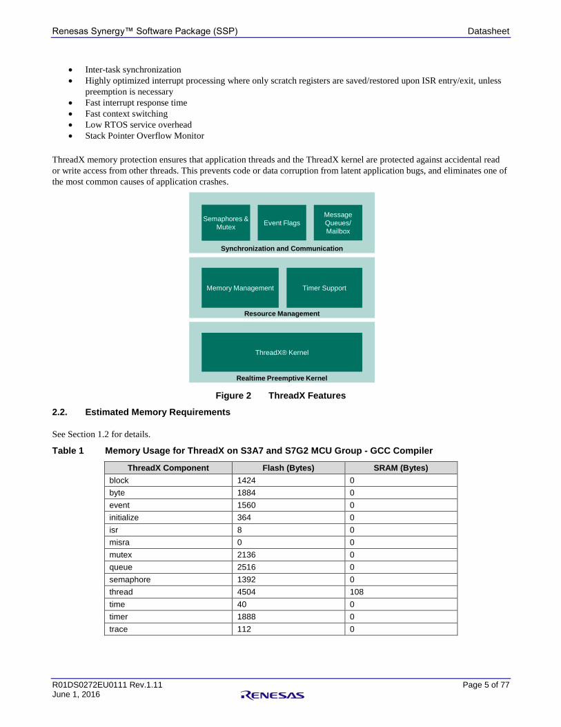
2. ThreadX® RTOS
2.1. Component Introduction
At the core of Renesas Synergy Software Package (SSP) is the industry-leading Express Logic, Inc. ThreadX RTOS. It is
optimized for MCUs in the Renesas Synergy family and tightly integrated with the SPP. ThreadX includes a completely
optimized, high-performance real-time kernel designed specifically for real-time embedded systems running on
microcontrollers, providing fast, sub-microsecond context switching and small, 2-KB memory footprint (Flash Memory).
The key features of ThreadX include:
Picokernel design where services are not layered
Preemptive and preemption-threshold scheduling
Event-chaining
Renesas Synergy™ Software Package (SSP) Datasheet
R01DS0272EU0111 Rev.1.11 Page 5 of 77 June 1, 2016
Inter-task synchronization
Highly optimized interrupt processing where only scratch registers are saved/restored upon ISR entry/exit, unless
preemption is necessary
Fast interrupt response time
Fast context switching
Low RTOS service overhead
Stack Pointer Overflow Monitor
ThreadX memory protection ensures that application threads and the ThreadX kernel are protected against accidental read
or write access from other threads. This prevents code or data corruption from latent application bugs, and eliminates one of
the most common causes of application crashes.
Figure 2 ThreadX Features
2.2. Estimated Memory Requirements
See Section 1.2 for details.
Table 1 Memory Usage for ThreadX on S3A7 and S7G2 MCU Group - GCC Compiler
ThreadX Component Flash (Bytes) SRAM (Bytes)
block 1424 0
byte 1884 0
event 1560 0
initialize 364 0
isr 8 0
misra 0 0
mutex 2136 0
queue 2516 0
semaphore 1392 0
thread 4504 108
time 40 0
timer 1888 0
trace 112 0
Realtime Preemptive Kernel
Synchronization and Communication
Resource Management
Memory Management Timer Support
Semaphores &
Mutex
Message
Queues/
Mailbox
Event Flags
ThreadX® Kernel
Renesas Synergy™ Software Package (SSP) Datasheet
R01DS0272EU0111 Rev.1.11 Page 6 of 77 June 1, 2016
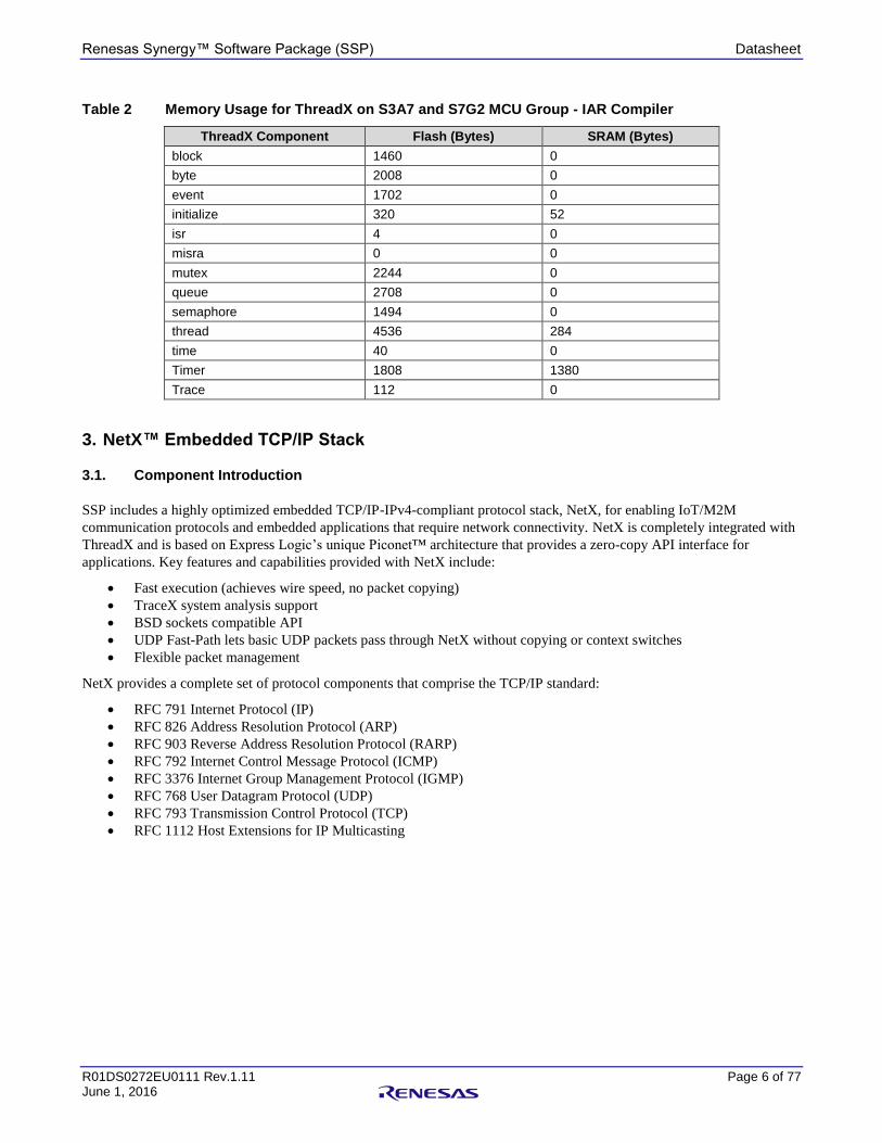
Table 2 Memory Usage for ThreadX on S3A7 and S7G2 MCU Group - IAR Compiler
ThreadX Component Flash (Bytes) SRAM (Bytes)
block 1460 0
byte 2008 0
event 1702 0
initialize 320 52
isr 4 0
misra 0 0
mutex 2244 0
queue 2708 0
semaphore 1494 0
thread 4536 284
time 40 0
Timer 1808 1380
Trace 112 0
3. NetX™ Embedded TCP/IP Stack
3.1. Component Introduction
SSP includes a highly optimized embedded TCP/IP-IPv4-compliant protocol stack, NetX, for enabling IoT/M2M
communication protocols and embedded applications that require network connectivity. NetX is completely integrated with
ThreadX and is based on Express Logic’s unique Piconet™ architecture that provides a zero-copy API interface for
applications. Key features and capabilities provided with NetX include:
Fast execution (achieves wire speed, no packet copying)
TraceX system analysis support
BSD sockets compatible API
UDP Fast-Path lets basic UDP packets pass through NetX without copying or context switches
Flexible packet management
NetX provides a complete set of protocol components that comprise the TCP/IP standard:
RFC 791 Internet Protocol (IP)
RFC 826 Address Resolution Protocol (ARP)
RFC 903 Reverse Address Resolution Protocol (RARP)
RFC 792 Internet Control Message Protocol (ICMP)
RFC 3376 Internet Group Management Protocol (IGMP)
RFC 768 User Datagram Protocol (UDP)
RFC 793 Transmission Control Protocol (TCP)
RFC 1112 Host Extensions for IP Multicasting
Renesas Synergy™ Software Package (SSP) Datasheet
R01DS0272EU0111 Rev.1.11 Page 7 of 77 June 1, 2016
Figure 3 IPv4/6 TCP/IP Stack
3.2. Estimated Memory Requirements
Estimated memory requirements for this section will be provided in future updates of this document.
4. NetX Duo™ Dual IPv4/IPv6 Stack
4.1. Component Introduction
For applications requiring IPv6 support, SSP includes Express Logic’s NetX Duo; a dual IPv4 and IPv6 compliant TCP/IP
protocol stack. NetX Duo is completely integrated with ThreadX RTOS and includes all features and capabilities available
with NetX, which further extends the capabilities of SSP-based devices to auto-configure their interface addresses through
the Stateless Address Auto configuration protocol. Devices can also use layered structures to enable devices to process IPv6
headers more efficiently. NetX Duo applications are individually selectable for each project providing flexibility to the
system designer to incorporate only the applications necessary for the target application.
NetX Duo implements the following protocols:
All IPv4 protocols available in NetX
Zero-copy API
UDP Fast Path Technology
BSD-compatible socket layer
RFC 2460 IPv6 Specification
RFC 4861 Neighbor Discovery for IPv6
RFC 4862 IPv6 Stateless Address Auto configuration
RFC 1981 Path MTU Discovery for IPv6
RFC 4443 ICMPv6
RFC 791 Internet Protocol (IP)
RFC 826 Address Resolution Protocol (ARP)
RFC 903 Reverse Address Resolution Protocol (RARP)
RFC 792 Internet Control Message Protocol (ICMP)
Ethernet
MAC Controller
NetX™/NetX™ Duo
Network Driver
IPv4/v6ICMPv4/v6 IGMP
ARP RARP
IPSec
TCP UDP
NetX™ Application Bundle
SSP
Synergy MCU

Renesas Synergy™ Software Package (SSP) Datasheet
R01DS0272EU0111 Rev.1.11 Page 8 of 77 June 1, 2016
RFC 3376 Internet Group Management Protocol (IGMP)
RFC 768 User Datagram Protocol (UDP)
RFC 793 Transmission Control Protocol (TCP)
RFC 1112 Host Extensions for IP Multicasting
NetX Duo has been accredited by the IPv6 forum with Phase-II IPv6-Ready Logo certification.
4.2. Estimated Memory Requirements
Estimated memory requirements for this section will be provided in future updates of this document.
5. NetXTM Applications Bundle
5.1. Component Introduction
Included with SSP are additional application layer protocols that are frequently used in networking devices:
Auto IP
o RFC 3927 Dynamic Configuration of IPv4 Link-Local Addresses
Dynamic Host Configuration Protocol for Servers (DHCP Server) and Client (DHCP Client)
o RFC 2131 Dynamic Host Configuration Protocol
o RFC 2132 DHCP Options and BOOTP Vendor Extensions
Domain Name System (DNS Client)
o RFC 1034 Domain Names – Concepts and Facilities
o RFC 1035 Domain names – Implementation and Specification
o RFC 1480 The US Domain
o RFC 2782 A DNS RR for specifying the location of services (DNS SRV)
HTTP Client and Webserver
o RFC 1945 Hypertext Transfer Protocol/1.0
o RFC 2616 Hypertext Transfer Protocol/1.1
o RFC 2581 TCP Congestion Control
o RFC 1122 Requirements for Internet Hosts - Communication Layers
RFC 959 FILE TRANSFER PROTOCOL (FTP) Client and Server
TFTP Client and Server
o RFC 1350 The TFTP Protocol (Revision 2)
Telnet Client and Server
o RFC 854 Telnet Protocol Specification
RFC 1939 Post Office Protocol - Version 3 (POP3)
RFC 1661 The Point-to-Point Protocol (PPP)
o RFC 1332 The PPP Internet Protocol Control Protocol (IPCP) o RFC1334 PPP Authentication Protocols o RFC1994 PPP Challenge Handshake Authentication Protocol (CHAP)
Simple Mail Transfer Protocol (SMTP)
o RFC 2821 Simple Mail Transfer Protocol (SMTP)
o RFC 2554 SMTP Service Extension for Authentication
RFC4330 Simple Network Time Protocol (SNTP) Version 4 for IPv4, IPv6 and OSI
These implementations of core networking protocols are thread-safe, compliant with respective RFCs/standards, and have
been optimized for memory footprint and CPU utilization. Networking applications are individually selectable for each
project providing flexibility to system designer to incorporate only applications necessary for the target application.
Renesas Synergy™ Software Package (SSP) Datasheet
R01DS0272EU0111 Rev.1.11 Page 9 of 77 June 1, 2016
5.2. Estimated Memory Requirements
Estimated memory requirements for this section will be provided in future updates of this document.
6. NetXTM Duo Applications Bundle
6.1. Component Introduction
Included with SSP are additional application layer protocols that are frequently used in networking devices:
Auto IP
o RFC 3927 Dynamic Configuration of IPv4 Link-Local Addresses
Dynamic Host Configuration Protocol for Servers (DHCP Server) and Client (DHCP Client)
o RFC 2131 Dynamic Host Configuration Protocol
o RFC 2132 DHCP Options and BOOTP Vendor Extensions
Domain Name System (DNS Client)
o RFC 1034 Domain Names – Concepts and Facilities
o RFC 1035 Domain names – Implementation and Specification
o RFC 1480 The US Domain
o RFC 2782 A DNS RR for specifying the location of services (DNS SRV)
HTTP Client and Webserver
o RFC 1945 Hypertext Transfer Protocol/1.0
o RFC 2616 Hypertext Transfer Protocol/1.1
o RFC 2581 TCP Congestion Control
o RFC 1122 Requirements for Internet Hosts - Communication Layers
RFC 959 FILE TRANSFER PROTOCOL (FTP) Client and Server
TFTP Client and Server
o RFC 1350 The TFTP Protocol (Revision 2)
Telnet Client and Server
o RFC 854 Telnet Protocol Specification
RFC 1939 Post Office Protocol - Version 3 (POP3)
RFC 1661 The Point-to-Point Protocol (PPP)
o RFC 1332 The PPP Internet Protocol Control Protocol (IPCP) o RFC1334 PPP Authentication Protocols o RFC1994 PPP Challenge Handshake Authentication Protocol (CHAP)
Simple Mail Transfer Protocol (SMTP)
o RFC 2821 Simple Mail Transfer Protocol (SMTP)
o RFC 2554 SMTP Service Extension for Authentication
RFC4330 Simple Network Time Protocol (SNTP) Version 4 for IPv4, IPv6 and OSI
These implementations of core networking protocols are thread-safe, compliant with respective RFCs/standards, and have
been optimized for memory footprint and CPU utilization. Networking applications are individually selectable for each
project providing flexibility to the system designer to incorporate only applications necessary for the target application.
6.2. Estimated Memory Requirements
Estimated memory requirements for this section will be provided in future updates of this document.
Renesas Synergy™ Software Package (SSP) Datasheet
R01DS0272EU0111 Rev.1.11 Page 10 of 77 June 1, 2016
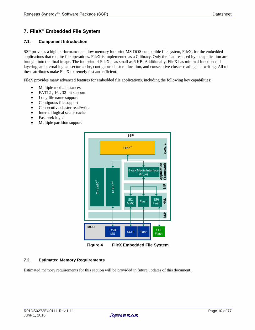
7. FileX® Embedded File System
7.1. Component Introduction
SSP provides a high performance and low memory footprint MS-DOS compatible file system, FileX, for the embedded
applications that require file operations. FileX is implemented as a C library. Only the features used by the application are
brought into the final image. The footprint of FileX is as small as 6 KB. Additionally, FileX has minimal function call
layering, an internal logical sector cache, contiguous cluster allocation, and consecutive cluster reading and writing. All of
these attributes make FileX extremely fast and efficient.
FileX provides many advanced features for embedded file applications, including the following key capabilities:
Multiple media instances
FAT12-, 16-, 32-bit support
Long file name support
Contiguous file support
Consecutive cluster read/write
Internal logical sector cache
Fast seek logic
Multiple partition support
Figure 4 FileX Embedded File System
7.2. Estimated Memory Requirements
Estimated memory requirements for this section will be provided in future updates of this document.
USB
MSSDHI Flash
SPI
Flash
HA
LSD/
MMCFlash
SPI
Flash
Ap
pli
cati
on
Fra
mew
ork
Block Media Interface
(fx_io)
X-W
are
FileX®
US
BX
™
Thre
adX
®
S/I
FB
SP
SSP
MCU
Renesas Synergy™ Software Package (SSP) Datasheet
R01DS0272EU0111 Rev.1.11 Page 11 of 77 June 1, 2016
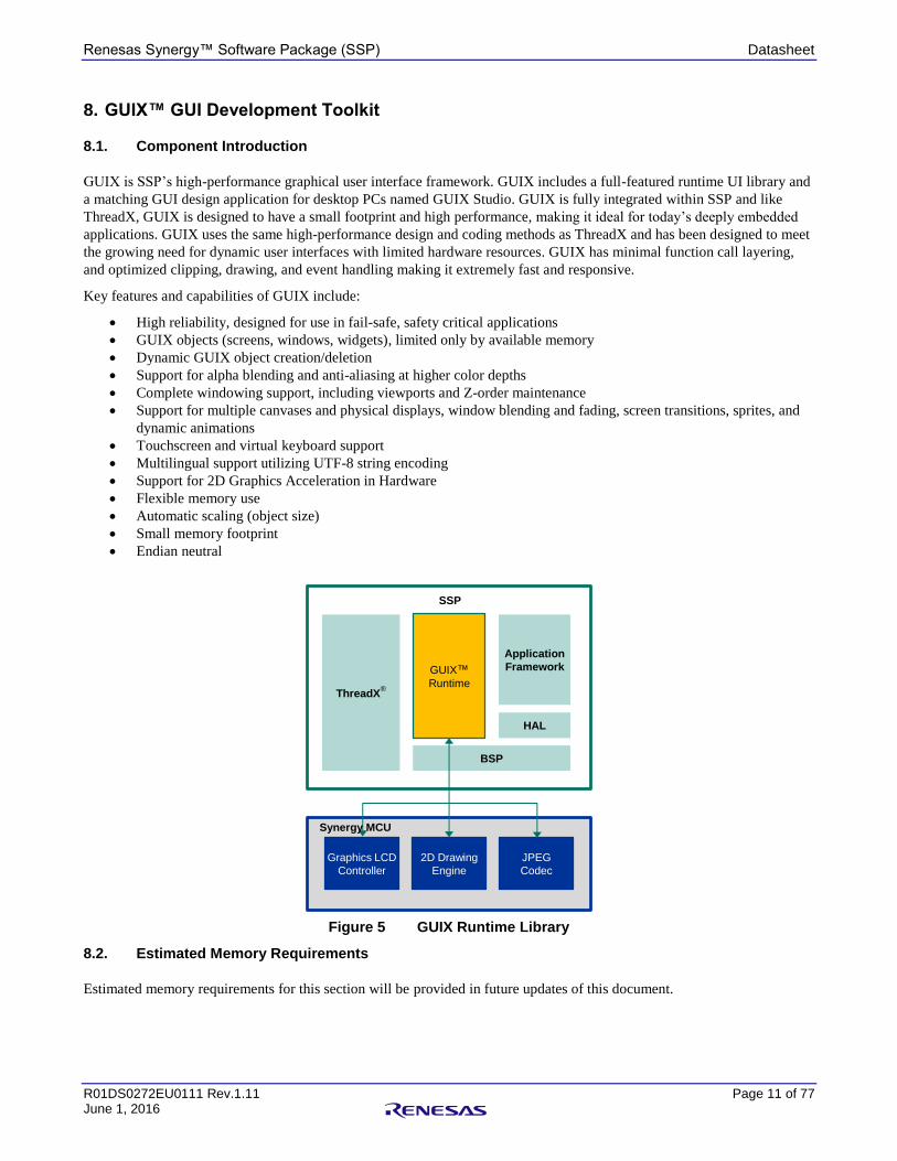
8. GUIX™ GUI Development Toolkit
8.1. Component Introduction
GUIX is SSP’s high-performance graphical user interface framework. GUIX includes a full-featured runtime UI library and
a matching GUI design application for desktop PCs named GUIX Studio. GUIX is fully integrated within SSP and like
ThreadX, GUIX is designed to have a small footprint and high performance, making it ideal for today’s deeply embedded
applications. GUIX uses the same high-performance design and coding methods as ThreadX and has been designed to meet
the growing need for dynamic user interfaces with limited hardware resources. GUIX has minimal function call layering,
and optimized clipping, drawing, and event handling making it extremely fast and responsive.
Key features and capabilities of GUIX include:
High reliability, designed for use in fail-safe, safety critical applications
GUIX objects (screens, windows, widgets), limited only by available memory
Dynamic GUIX object creation/deletion
Support for alpha blending and anti-aliasing at higher color depths
Complete windowing support, including viewports and Z-order maintenance
Support for multiple canvases and physical displays, window blending and fading, screen transitions, sprites, and
dynamic animations
Touchscreen and virtual keyboard support
Multilingual support utilizing UTF-8 string encoding
Support for 2D Graphics Acceleration in Hardware
Flexible memory use
Automatic scaling (object size)
Small memory footprint
Endian neutral
Figure 5 GUIX Runtime Library
8.2. Estimated Memory Requirements
Estimated memory requirements for this section will be provided in future updates of this document.
BSP
ThreadX®
GUIX™Runtime
Application
Framework
HAL
Graphics LCD
Controller
2D Drawing
Engine
JPEG
Codec
SSP
Synergy MCU
Renesas Synergy™ Software Package (SSP) Datasheet
R01DS0272EU0111 Rev.1.11 Page 12 of 77 June 1, 2016
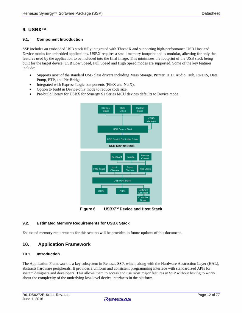
9. USBX™
9.1. Component Introduction
SSP includes an embedded USB stack fully integrated with ThreadX and supporting high-performance USB Host and
Device modes for embedded applications. USBX requires a small memory footprint and is modular, allowing for only the
features used by the application to be included into the final image. This minimizes the footprint of the USB stack being
built for the target device. USB Low Speed, Full Speed and High Speed modes are supported. Some of the key features
include:
Supports most of the standard USB class drivers including Mass Storage, Printer, HID, Audio, Hub, RNDIS, Data
Pump, PTP, and PictBridge.
Integrated with Express Logic components (FileX and NetX).
Option to build in Device-only mode to reduce code size.
Pre-build library for USBX for Synergy S1 Series MCU devices defaults to Device mode.
Figure 6 USBXTM Device and Host Stack
9.2. Estimated Memory Requirements for USBX Stack
Estimated memory requirements for this section will be provided in future updates of this document.
10. Application Framework
10.1. Introduction
The Application Framework is a key subsystem in Renesas SSP, which, along with the Hardware Abstraction Layer (HAL),
abstracts hardware peripherals. It provides a uniform and consistent programming interface with standardized APIs for
system designers and developers. This allows them to access and use most major features in SSP without having to worry
about the complexity of the underlying low-level device interfaces in the platform.
USB Device Controller Driver
VBUS
Manager
USB Device Stack
Storage
Class
CDC
Class
Custom
Class
Controller
Driver
Software
ScheduleEHCIOHCI
USB Host Stack
HUB ClassIsoch
Classes
Async
ClassesHID Class
Remote
ControlMouseKeyboard
USB Device Stack

Renesas Synergy™ Software Package (SSP) Datasheet
R01DS0272EU0111 Rev.1.11 Page 13 of 77 June 1, 2016
The Application Framework is tightly integrated with ThreadX, provides thread-safe APIs for accessing shared resources,
and manages access conflicts by providing mutual exclusion and synchronization services amongst application tasks.
The Application Framework in SSP links the RTOS with HAL and provides high-level, C-callable interfaces for commonly
used platform system services.
Figure 7 Application Framework
10.2. Audio Playback Framework
10.2.1. Component Introduction
The Audio Playback Framework in SSP provides standardized, C-callable, high-level APIs for playback of audio content.
The framework handles the integration and synchronization of multiple HAL peripherals like timers, DMA, and DAC to
facilitate audio playback. The Audio Playback Framework APIs are thread-safe and abstract underlying MCU hardware
features; for example, timers, Sampling Rate Convertor, and DACs. The Audio Playback Framework supports 16-bit mono
uncompressed (linear) PCM samples and lets developers plug in custom components. The framework supports single
instantiation.
Playback control features provided with Audio Framework:
Open audio device for audio playback.
Close audio device opened for audio playback.
Start audio playback.
Stop audio playback.
Pause audio playback. Resume audio playback.
Set software volume control.
Audio Playback Framework supports following output peripherals:
DAC
PWM
Audio Playback Framework features:
Application Program
Application Framework
Audio
Console
JPEG
Touch Panel
External IRQ
Messaging
BSP
HAL
ThreadX®
X-Ware™
SSP
Synergy
MCU
SPI
IIC
UART
Thread Monitor
Power Profile
Others

Renesas Synergy™ Software Package (SSP) Datasheet
R01DS0272EU0111 Rev.1.11 Page 14 of 77 June 1, 2016
Plays long buffers by splitting the data into smaller manageable blocks.
Repeat/loop playback of supplied audio data until ThreadX timeout.
Can request next data using callback after last buffer playback begins.
Scaling to playback signed 16-bit PCM samples through unsigned 12-bit DAC.
Basic mixing of multiple streams.
The Audio Playback Framework does not support reading files in a file system and decoding audio. These
functions are performed outside of the Audio Playback Framework.
Figure 8 Audio Playback Framework
10.2.2. Estimated Memory Requirements
See Section 1.2 for details.
Table 3 Memory Usage for Audio Playback Framework - GCC Compiler
sf_audio_playback Flash (Bytes) SRAM (Bytes)
S7G2 MCU Group 3,095 0
S3A7 MCU Group 3,095 0
S124 MCU Group 3,247 0
Table 4 Memory Usage for Audio Playback Framework - IAR Compiler
sf_audio_playback Flash (Bytes) SRAM (Bytes)
S7G2 MCU Group 3,140 0
S3A7 MCU Group 3,140 0
S124 MCU Group 3,288 0
10.3. Inter-Thread Messaging Framework
10.3.1. Component Introduction
The Inter-Thread Messaging Framework in SSP provides easy to use high-level APIs for inter-thread communication and
synchronization. The Inter-Thread Messaging Framework implements a lightweight, event-driven message-passing
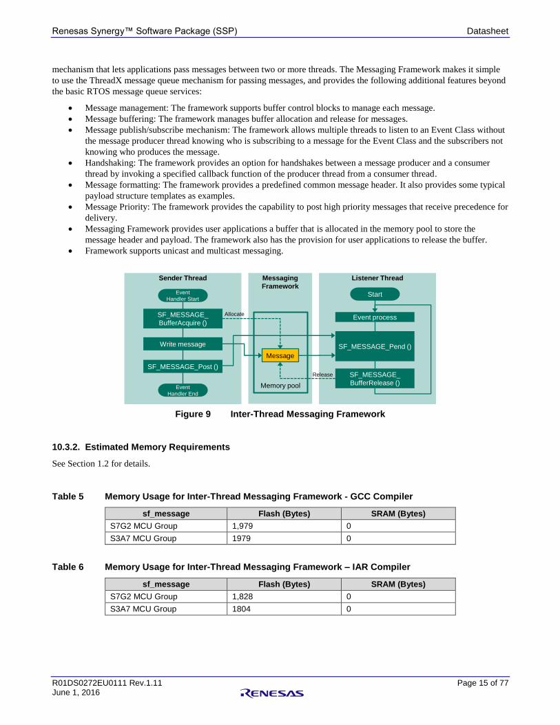
Renesas Synergy™ Software Package (SSP) Datasheet
R01DS0272EU0111 Rev.1.11 Page 15 of 77 June 1, 2016
mechanism that lets applications pass messages between two or more threads. The Messaging Framework makes it simple
to use the ThreadX message queue mechanism for passing messages, and provides the following additional features beyond
the basic RTOS message queue services:
Message management: The framework supports buffer control blocks to manage each message.
Message buffering: The framework manages buffer allocation and release for messages.
Message publish/subscribe mechanism: The framework allows multiple threads to listen to an Event Class without
the message producer thread knowing who is subscribing to a message for the Event Class and the subscribers not
knowing who produces the message.
Handshaking: The framework provides an option for handshakes between a message producer and a consumer
thread by invoking a specified callback function of the producer thread from a consumer thread.
Message formatting: The framework provides a predefined common message header. It also provides some typical
payload structure templates as examples.
Message Priority: The framework provides the capability to post high priority messages that receive precedence for
delivery.
Messaging Framework provides user applications a buffer that is allocated in the memory pool to store the
message header and payload. The framework also has the provision for user applications to release the buffer.
Framework supports unicast and multicast messaging.
Figure 9 Inter-Thread Messaging Framework
10.3.2. Estimated Memory Requirements
See Section 1.2 for details.
Table 5 Memory Usage for Inter-Thread Messaging Framework - GCC Compiler
sf_message Flash (Bytes) SRAM (Bytes)
S7G2 MCU Group 1,979 0
S3A7 MCU Group 1979 0
Table 6 Memory Usage for Inter-Thread Messaging Framework – IAR Compiler
sf_message Flash (Bytes) SRAM (Bytes)
S7G2 MCU Group 1,828 0
S3A7 MCU Group 1804 0
Listener ThreadSender Thread Messaging
Framework
Memory pool
SF_MESSAGE_Pend ()
SF_MESSAGE_
BufferRelease ()
Message
StartEvent
Handler Start
SF_MESSAGE_
BufferAcquire ()
Write message
SF_MESSAGE_Post ()
Event
Handler End
Event processAllocate
Release

Renesas Synergy™ Software Package (SSP) Datasheet
R01DS0272EU0111 Rev.1.11 Page 16 of 77 June 1, 2016
10.4. I2C Framework
10.4.1. Component Introduction
The I2C Framework in SSP abstracts the software interface for the I2C driver. It provides a simple, high-level, C-callable
API for seamless and thread-safe access of the I2C interface from multiple application threads.
The I2C framework is ThreadX aware and handles the integration and synchronization of multiple I2C peripherals on an I2C
bus. The I2C Framework enables the user to create one or more I2C buses and connect multiple I2C peripherals to the buses.
The I2C Framework makes use of low-level I2C driver modules and SCI common driver modules to communicate with I2C
peripherals. The I2C Framework provides Mutual Exclusion and Synchronization services to manage simultaneous multiple
access requests. Internally the framework uses ThreadX objects like mutex bus locking/unlocking for blocking, and
synchronization techniques like event flags for completion of transactions. The I2C Framework supports the handling of
restart condition and provides common interface for both SCI I2C and RIIC peripherals.
The framework blocks access to a specific channel while in use with mutex.
The framework driver handles callback to notify application of events.
The framework maintains a counter that tracks how many devices are currently on the bus.
The framework also provides timeout parameter to the write/read API functions.
The framework provides lock options to lock a bus for a device and provides an unlock API to unlock the locked
bus by device.
The framework supports all channels available with the device.
Framework supports opening of multiple devices on the same bus.
Figure 10 I2C Framework
Renesas Synergy™ Software Package (SSP) Datasheet
R01DS0272EU0111 Rev.1.11 Page 17 of 77 June 1, 2016
10.4.2. Estimated Memory Requirements
See Section 1.2 for details.
Table 7 Memory Use for I2C Framework – GCC Compiler
sf_i2c Flash (Bytes) SRAM (Bytes)
S7G2 MCU Group 1,453 0
S3A7 MCU Group 1,453 0
S124 MCU Group 1,457 0
Table 8 Memory Use for I2C Framework – IAR Compiler
sf_i2c Flash (Bytes) SRAM (Bytes)
S7G2 MCU Group 1,340 0
S3A7 MCU Group 1,340 0
S124 MCU Group 1,348
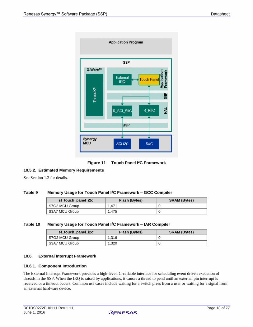
10.5. Touch Panel I2C Framework
10.5.1. Component Introduction
The Touch Panel I2C Framework in SSP provides a high-level, C-callable programmable interface for interfacing with
external touch screen controllers. Internally the Touch Panel I2C Framework uses I2C to interface with the touch screen
controller. The Touch Panel I2C Framework API provides seamless and thread-safe software interface for touch screens
from SSP.
The Touch Panel I2C Framework is commonly used for capturing touch input for GUI applications. It produces touch data
messages with position information (X and Y coordinates) and event type information which are posted to event queue(s)
using the Messaging Framework. The touch panel framework also creates a thread to poll the touch driver and post touch
data to the Messaging Framework.
The Touch Panel I2C Framework sequentially processes UI input events in the order they are received from the I2C
interface. The framework supports receiving input events from multiple touch screens. Internally the framework uses mutex
for synchronization between multiple application threads. The framework uses external interrupt interface for
synchronization.
The API has provisions for:
Specifying the display resolution.
Limiting the rate of touch messages published for positioning information.
Interrupt driven I2C touch controller chips.
Configuring minimum period between touch messages for repeat events (hold/move).
A calibrate function for ADC interface calibration.
An option to start and stop touch processing. When stopped the Framework terminates all underlying low level
drivers used by the touch panel framework. Additionally the framework provides a reset function for runtime reset.
The touch panel framework supports touch controllers available on all Renesas Product Examples and Development Kits.
Renesas Synergy™ Software Package (SSP) Datasheet
R01DS0272EU0111 Rev.1.11 Page 18 of 77 June 1, 2016
Figure 11 Touch Panel I2C Framework
10.5.2. Estimated Memory Requirements
See Section 1.2 for details.
Table 9 Memory Usage for Touch Panel I2C Framework – GCC Compiler
sf_touch_panel_i2c Flash (Bytes) SRAM (Bytes)
S7G2 MCU Group 1,471 0
S3A7 MCU Group 1,475 0
Table 10 Memory Usage for Touch Panel I2C Framework – IAR Compiler
sf_touch_panel_i2c Flash (Bytes) SRAM (Bytes)
S7G2 MCU Group 1,316 0
S3A7 MCU Group 1,320 0
10.6. External Interrupt Framework
10.6.1. Component Introduction
The External Interrupt Framework provides a high-level, C-callable interface for scheduling event driven execution of
threads in the SSP. When the IRQ is raised by applications, it causes a thread to pend until an external pin interrupt is
received or a timeout occurs. Common use cases include waiting for a switch press from a user or waiting for a signal from
an external hardware device.

Renesas Synergy™ Software Package (SSP) Datasheet
R01DS0272EU0111 Rev.1.11 Page 19 of 77 June 1, 2016
The interrupt framework is ThreadX aware and provides generic external interrupt handling capability. The APIs for
Interrupt Framework are thread-safe and internally the framework uses ThreadX objects like mutex for blocking, and
synchronization techniques like semaphores for interrupt handling by multiple application threads. Some of the key features
include:
Supports unique pending IRQ requests for multiple threads.
Supports IRQ requests for up to 16 hardware channels.
Provides programmable timeout for wait function through the APIs.
Thread can be suspended while waiting for external IRQ request.
Provides provision to specify timeouts.
Configures the driver to block access to specific low level external IRQ when it is being accessed using mutex.
Provides API which waits for an external IRQ to be triggered.
Makes use of lower level HAL driver for interfacing to the external IRQ hardware.
Figure 12 External Interrupt Framework
10.6.2. Estimated Memory Requirements
See Section 1.2 for details.
Renesas Synergy™ Software Package (SSP) Datasheet
R01DS0272EU0111 Rev.1.11 Page 20 of 77 June 1, 2016
Table 11 Memory Usage for External Interrupt Framework – GCC Compiler
sf_external_irq Flash (Bytes) SRAM (Bytes)
S7G2 MCU Group 744 0
S3A7 MCU Group 744 0
S124 MCU Group 748 0
Table 12 Memory Usage for External Interrupt Framework – IAR Compiler
sf_external_irq Flash (Bytes) SRAM (Bytes)
S7G2 MCU Group 624 0
S3A7 MCU Group 624 0
S124 MCU Group 644 0
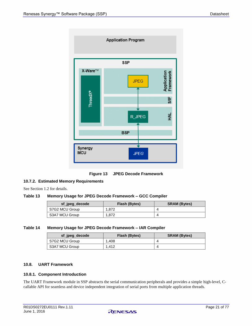
10.7. JPEG Decode Framework
10.7.1. Component Introduction
The JPEG Decode Framework module in SSP abstracts the on-chip JPEG codec and provides a simple high-level, C-
callable API for seamless and device independent integration of JPEG decoder application threads. The JPEG codec allows
for high-speed compression of raw images and decoding of JPEG images. The codec conforms to the JPEG baseline
compression and decompression standard, JPEG Part 2, ISO-IEC 10918-2.
The JPEG Decode Framework is ThreadX aware and provides primary JPEG decoder functionality. The JPEG APIs are
thread-safe and internally the framework uses ThreadX objects like mutex for blocking, and synchronization techniques,
like event flags for completion of JPEG data decompression by multiple application threads.
The JPEG Decode Framework APIs handles the decode tasks by taking application specific encoded data in an input buffer
and allocating an output buffer pointer to store the decoded image frame. Alternatively, the API can handle streaming
encoded data into JPEG decoder module. This feature allows an application to read encoded JPEG image from a file or
from network without buffering the entire image. The framework allows the application to specify the number of image
lines to decode so that the application can decode the image on the fly without buffering the entire frame.
Renesas Synergy™ Software Package (SSP) Datasheet
R01DS0272EU0111 Rev.1.11 Page 21 of 77 June 1, 2016
Figure 13 JPEG Decode Framework
10.7.2. Estimated Memory Requirements
See Section 1.2 for details.
Table 13 Memory Usage for JPEG Decode Framework – GCC Compiler
sf_jpeg_decode Flash (Bytes) SRAM (Bytes)
S7G2 MCU Group 1,872 4
S3A7 MCU Group 1,872 4
Table 14 Memory Usage for JPEG Decode Framework – IAR Compiler
sf_jpeg_decode Flash (Bytes) SRAM (Bytes)
S7G2 MCU Group 1,408 4
S3A7 MCU Group 1,412 4
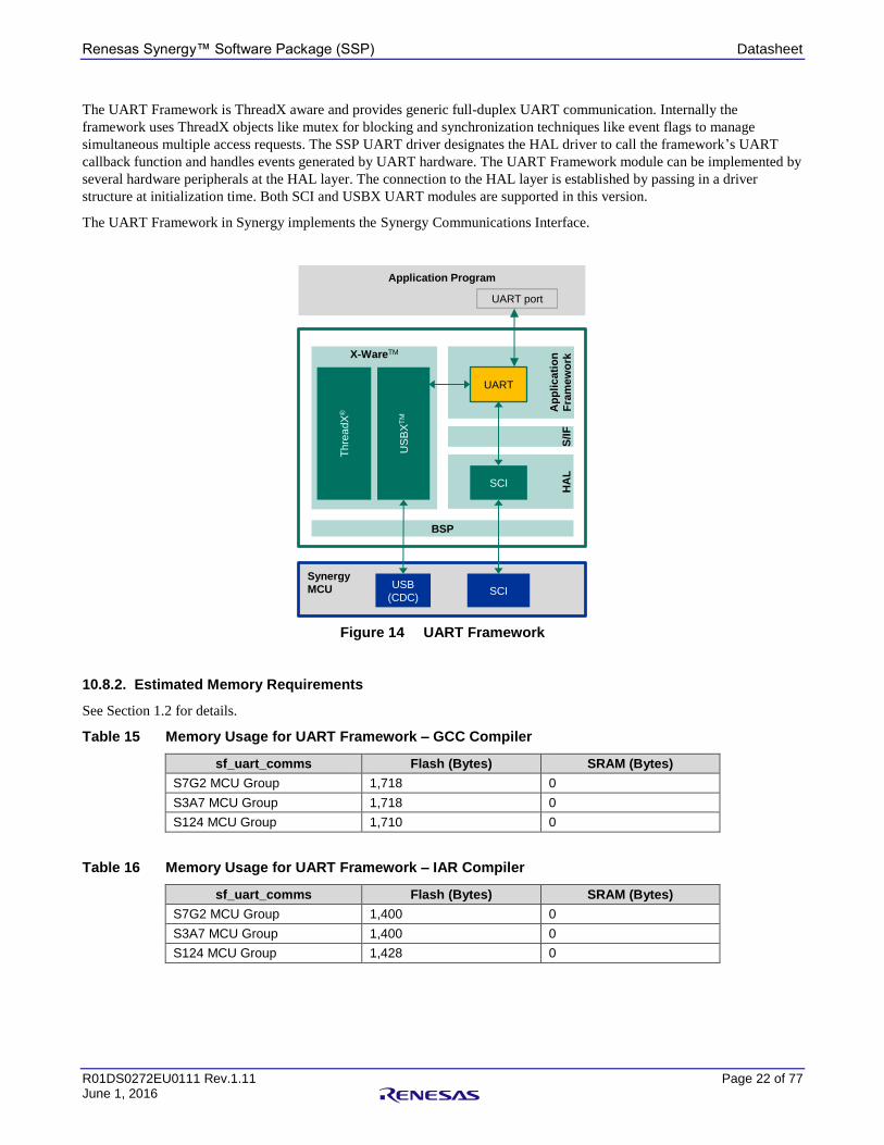
10.8. UART Framework
10.8.1. Component Introduction
The UART Framework module in SSP abstracts the serial communication peripherals and provides a simple high-level, C-
callable API for seamless and device independent integration of serial ports from multiple application threads.
Renesas Synergy™ Software Package (SSP) Datasheet
R01DS0272EU0111 Rev.1.11 Page 22 of 77 June 1, 2016
The UART Framework is ThreadX aware and provides generic full-duplex UART communication. Internally the
framework uses ThreadX objects like mutex for blocking and synchronization techniques like event flags to manage
simultaneous multiple access requests. The SSP UART driver designates the HAL driver to call the framework’s UART
callback function and handles events generated by UART hardware. The UART Framework module can be implemented by
several hardware peripherals at the HAL layer. The connection to the HAL layer is established by passing in a driver
structure at initialization time. Both SCI and USBX UART modules are supported in this version.
The UART Framework in Synergy implements the Synergy Communications Interface.
Figure 14 UART Framework
10.8.2. Estimated Memory Requirements
See Section 1.2 for details.
Table 15 Memory Usage for UART Framework – GCC Compiler
sf_uart_comms Flash (Bytes) SRAM (Bytes)
S7G2 MCU Group 1,718 0
S3A7 MCU Group 1,718 0
S124 MCU Group 1,710 0
Table 16 Memory Usage for UART Framework – IAR Compiler
sf_uart_comms Flash (Bytes) SRAM (Bytes)
S7G2 MCU Group 1,400 0
S3A7 MCU Group 1,400 0
S124 MCU Group 1,428 0
Application Program
UART port
HA
L
SCI
Ap
pli
ca
tio
n
Fra
mew
ork
UART
BSP
X-WareTM
US
BX
TM
Thre
adX
®
S/I
F
SCIUSB
(CDC)
Synergy
MCU

Renesas Synergy™ Software Package (SSP) Datasheet
R01DS0272EU0111 Rev.1.11 Page 23 of 77 June 1, 2016
10.9. Console Framework
10.9.1. Component Introduction
The Console Framework module in SSP provides easy to use high-level, C-callable APIs for implementing a CLI
(command line interface). The framework defines command names and callback function for each command, and uses the
Communications Framework to receive commands and input strings, parse the content, and invoke the relevant command
handler routine.
The Console Framework can handle inputs from other serial interfaces as well; for example, USB CDC. The parser within
the framework provides support for nested menus, standard commands to return to the root menu (“~”) and to back out to
the previous menu (“..”). It also supports arrow key input, backspace, and delete keys.
The Console Framework supports hierarchical menus and parsing of input command based on predefined command list.
The framework provides notification when a command is selected and provides an error code if the command isn't found.
The Console Framework supports:
Input without parsing
Numerical input
Echo option to echo input to transmitter
Backspace and arrow key navigation
UART driver and other serial drivers
Figure 15 Console Framework
10.9.2. Estimated Memory Requirements
See Section 1.2 for details.
Table 17 Memory Usage for Console Framework – GCC Compiler
sf_console Flash (Bytes) SRAM (Bytes)
S7G2 MCU Group 2,480 5
S3A7 MCU Group 2,480 5
S124 MCU Group 2,476 5
Application Program
Callback for Command
Start
SF_CONSOLE_Prompt ()
SF_CONSOLE_Open ()
Console Framework
Start
Read UART
Parse
command

Renesas Synergy™ Software Package (SSP) Datasheet
R01DS0272EU0111 Rev.1.11 Page 24 of 77 June 1, 2016
Table 18 Memory Usage for Console Framework – IAR Compiler
sf_console Flash (Bytes) SRAM (Bytes)
S7G2 MCU Group 2,336 8
S3A7 MCU Group 2,336 8
S124 MCU Group 2,364 8
10.10. Thread Monitor Framework
10.10.1. Component Introduction
The Thread Monitor Framework monitors RTOS threads using a Watchdog Timer (WDT). The Thread Monitor forces a
watchdog reset of the microcontroller when any of the monitored threads misbehave.
The Thread Monitor operates as follows:
A thread registers a counter variable with the Thread Monitor Framework along with minimum and maximum expected
values for this counter variable. The thread which is monitored increments the counter variable while it runs. At a period of
half the watchdog timeout period, the Thread Monitor checks the counter variables of registered threads. If any fall outside
of the minimum and maximum values, the Watchdog Timer is allowed to reset the microcontroller.
If the counter variables fall within their expected range, the Watchdog Timer is refreshed and the counter values are cleared
to zero. In profiling mode, the minimum and maximum counter values for registered threads can be determined. In profiling
mode, the (WDT) is always refreshed and therefore does not reset the device. The framework supports both the Watchdog
Timer and the Independent Watchdog Timer (IWDT) HAL modules.
Figure 16 Thread Monitor Timing Chart

Renesas Synergy™ Software Package (SSP) Datasheet
R01DS0272EU0111 Rev.1.11 Page 25 of 77 June 1, 2016
Figure 17 Thread Monitor Flow Chart
10.10.2. Estimated Memory Requirements
See Section 1.2 for details.
Table 19 Memory Usage for Thread Monitor Framework – GCC Compiler
sf_thread_monitor Flash (Bytes) SRAM (Bytes)
S7G2 MCU Group 1,415 0
S3A7 MCU Group 1,415 0
S124 MCU Group 1,491 0
Table 20 Memory Usage for Thread Monitor Framework – IAR Compiler
sf_thread_monitor Flash (Bytes) SRAM (Bytes)
S7G2 MCU Group 1,328 0
S3A7 MCU Group 1,328 0
S124 MCU Group 1,324 0
Renesas Synergy™ Software Package (SSP) Datasheet
R01DS0272EU0111 Rev.1.11 Page 26 of 77 June 1, 2016
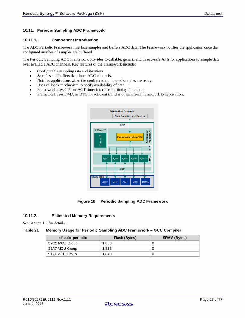
10.11. Periodic Sampling ADC Framework
10.11.1. Component Introduction
The ADC Periodic Framework Interface samples and buffers ADC data. The Framework notifies the application once the
configured number of samples are buffered.
The Periodic Sampling ADC Framework provides C-callable, generic and thread-safe APIs for applications to sample data
over available ADC channels. Key features of the Framework include:
Configurable sampling rate and iterations.
Samples and buffers data from ADC channels.
Notifies applications when the configured number of samples are ready.
Uses callback mechanism to notify availability of data.
Framework uses GPT or AGT timer interface for timing functions.
Framework uses DMA or DTC for efficient transfer of data from framework to application.
Figure 18 Periodic Sampling ADC Framework
10.11.2. Estimated Memory Requirements
See Section 1.2 for details.
Table 21 Memory Usage for Periodic Sampling ADC Framework – GCC Compiler
sf_adc_periodic Flash (Bytes) SRAM (Bytes)
S7G2 MCU Group 1,856 0
S3A7 MCU Group 1,856 0
S124 MCU Group 1,840 0

Renesas Synergy™ Software Package (SSP) Datasheet
R01DS0272EU0111 Rev.1.11 Page 27 of 77 June 1, 2016
Table 22 Memory Usage for Periodic Sampling ADC Framework – IAR Compiler
sf_adc_periodic Flash (Bytes) SRAM (Bytes)
S7G2 MCU Group 1,432 0
S3A7 MCU Group 1,432 0
S124 MCU Group 1,472 0
10.12. Audio Playback HW DAC Framework
10.12.1. Component Introduction
The Audio Playback HW DAC Framework handles the integration and synchronization of multiple HAL peripherals like
timers, DMA, and DAC to facilitate audio playback. This light-eight framework provides basic audio playback
functionality and can be used for short tones or chirps. For advanced audio applications, this framework is typically used
with the Audio Playback Framework.
Audio Playback HW DAC Framework features include:
Plays a single buffer of pre-scaled 12 bit unsigned PCM audio samples.
Provides information about the required data type (12 bit unsigned).
Provides callback mechanism to notify application when buffer has finished playing.
Configures the audio hardware based on application settings.
Play long buffers by splitting the data into manageable chunks.
Repeat playback until ThreadX timeout (for repeated audio like sine wave tones or looped background music).
Request next data using callback after last buffer playback begins.
Software volume control.
Pause and resume functions.
Scaling to move signed 16-bit PCM data into range of the unsigned 12-bit DAC.
Basic mixing for multiple streams.
The framework supports playing back of multiple streams on a single hardware port.
Figure 19 Audio Playback HW DAC Framework

Renesas Synergy™ Software Package (SSP) Datasheet
R01DS0272EU0111 Rev.1.11 Page 28 of 77 June 1, 2016
10.12.2. Estimated Memory Requirements
See Section 1.2 for details.
Table 23 Memory Usage for Audio Playback HW DAC Framework – GCC Compiler
sf_audio_playback_hw_dac Flash (Bytes) SRAM (Bytes)
S7G2 MCU Group 1,411 28
S3A7 MCU Group 1,411 28
S124 MCU Group 1,491 28
Table 24 Memory Usage for Audio Playback HW DAC Framework – IAR Compiler
sf_audio_playback_hw_dac Flash (Bytes) SRAM (Bytes)
S7G2 MCU Group 1,076 28
S3A7 MCU Group 1,076 28
S124 MCU Group 1,100 28
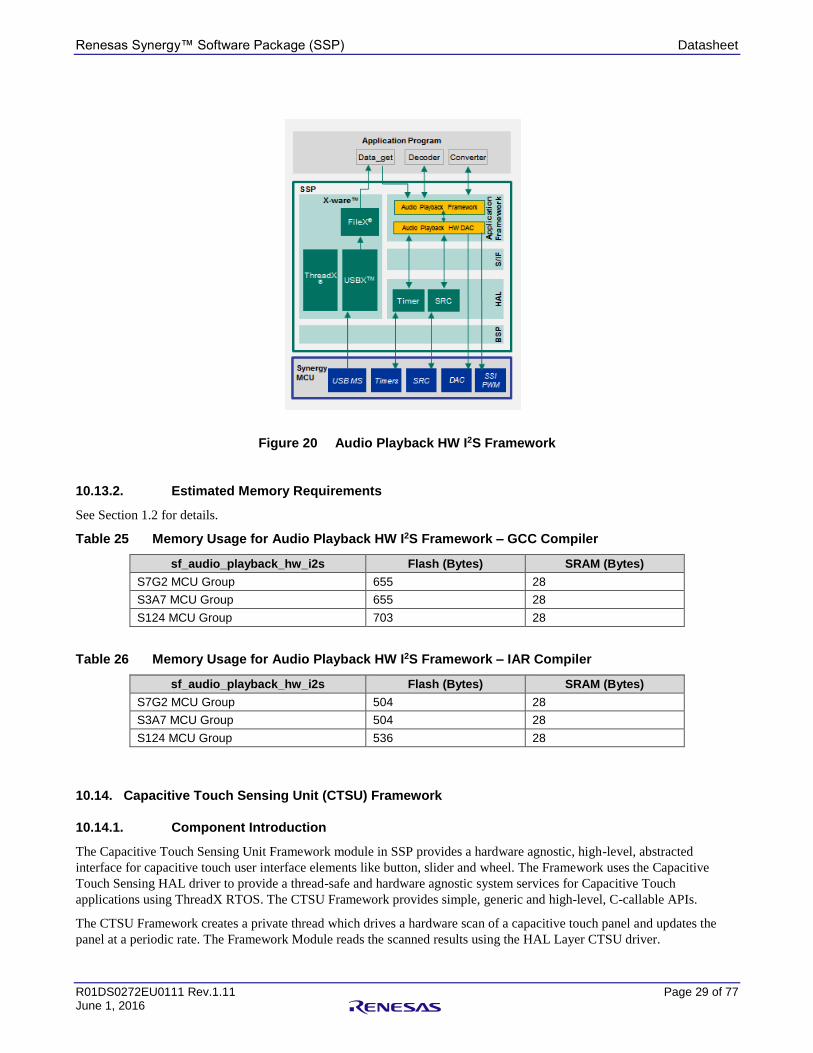
10.13. Audio Playback HW I2S Framework
10.13.1. Component Introduction
The Audio Playback HW I2S Framework handles the integration and synchronization of multiple HAL peripherals like
timers, DMA, and I2S to facilitate audio playback. This light-eight framework provides basic audio playback functionality
and can be used for short tones or chirps. For advanced audio applications, this framework is typically used with the Audio
Playback Framework.
Audio Playback HW I2S Framework features include:
Plays a single buffer of pre-scaled 12 bit unsigned PCM audio samples.
Provides information about the required data type (12 bit unsigned).
Provides callback mechanism to notify application when buffer has finished playing.
Configures the audio hardware based on application settings
Play long buffers by splitting the data into manageable chunks.
Repeat playback until ThreadX timeout (for repeated audio like sine wave tones or looped background music).
Request next data using callback after last buffer playback begins.
Software volume control.
Pause and resume functions.
Scaling to move signed 16-bit PCM data into range of the unsigned 12-bit DAC.
Basic mixing for multiple streams.
The framework supports playing back of multiple streams on a single hardware port.
Renesas Synergy™ Software Package (SSP) Datasheet
R01DS0272EU0111 Rev.1.11 Page 29 of 77 June 1, 2016
Figure 20 Audio Playback HW I2S Framework
10.13.2. Estimated Memory Requirements
See Section 1.2 for details.
Table 25 Memory Usage for Audio Playback HW I2S Framework – GCC Compiler
sf_audio_playback_hw_i2s Flash (Bytes) SRAM (Bytes)
S7G2 MCU Group 655 28
S3A7 MCU Group 655 28
S124 MCU Group 703 28
Table 26 Memory Usage for Audio Playback HW I2S Framework – IAR Compiler
sf_audio_playback_hw_i2s Flash (Bytes) SRAM (Bytes)
S7G2 MCU Group 504 28
S3A7 MCU Group 504 28
S124 MCU Group 536 28
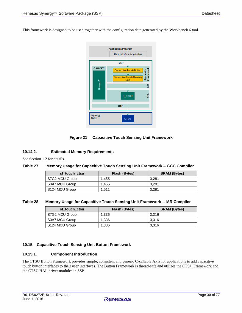
10.14. Capacitive Touch Sensing Unit (CTSU) Framework
10.14.1. Component Introduction
The Capacitive Touch Sensing Unit Framework module in SSP provides a hardware agnostic, high-level, abstracted
interface for capacitive touch user interface elements like button, slider and wheel. The Framework uses the Capacitive
Touch Sensing HAL driver to provide a thread-safe and hardware agnostic system services for Capacitive Touch
applications using ThreadX RTOS. The CTSU Framework provides simple, generic and high-level, C-callable APIs.
The CTSU Framework creates a private thread which drives a hardware scan of a capacitive touch panel and updates the
panel at a periodic rate. The Framework Module reads the scanned results using the HAL Layer CTSU driver.
Renesas Synergy™ Software Package (SSP) Datasheet
R01DS0272EU0111 Rev.1.11 Page 30 of 77 June 1, 2016
This framework is designed to be used together with the configuration data generated by the Workbench 6 tool.
Figure 21 Capacitive Touch Sensing Unit Framework
10.14.2. Estimated Memory Requirements
See Section 1.2 for details.
Table 27 Memory Usage for Capacitive Touch Sensing Unit Framework – GCC Compiler
sf_touch_ctsu Flash (Bytes) SRAM (Bytes)
S7G2 MCU Group 1,455 3,281
S3A7 MCU Group 1,455 3,281
S124 MCU Group 1,511 3,281
Table 28 Memory Usage for Capacitive Touch Sensing Unit Framework – IAR Compiler
sf_touch_ctsu Flash (Bytes) SRAM (Bytes)
S7G2 MCU Group 1,336 3,316
S3A7 MCU Group 1,336 3,316
S124 MCU Group 1,336 3,316
10.15. Capacitive Touch Sensing Unit Button Framework
10.15.1. Component Introduction
The CTSU Button Framework provides simple, consistent and generic C-callable APIs for applications to add capacitive
touch button interfaces to their user interfaces. The Button Framework is thread-safe and utilizes the CTSU Framework and
the CTSU HAL driver modules in SSP.

Renesas Synergy™ Software Package (SSP) Datasheet
R01DS0272EU0111 Rev.1.11 Page 31 of 77 June 1, 2016
The CTSU Button Framework interprets the data received from the CTSU Framework for all buttons that are present in the
system. It also initializes the CTSU Framework layer and registers a callback with the CTSU Framework layer which will
be called each time processed data is available. The CTSU Button Framework then uses this processed data to perform de-
bouncing and determine which of the configured events (Press, Release, Long Touch, etc.) has occurred for each button and
calls the callback for each button in the order in which they are present in the button configuration table.
CTSU Button Framework supports the following gestures for the button interface:
Pressed State
Released State
Long Touch
Short Touch
Multi Touch
Button is stuck in pressed state
The framework is designed to be used together with configuration data generated by the Workbench 6 tool.
10.15.2. Estimated Memory Requirements
See Section 1.2 for details.
Table 29 Memory Usage for Capacitive Touch Sensing Unit Button Framework – GCC Compiler
sf_touch_ctsu_button Flash (Bytes) SRAM (Bytes)
S7G2 MCU Group 2,425 0
S3A7 MCU Group 2,425 0
S124 MCU Group 2,309 0
Table 30 Memory Usage for Capacitive Touch Sensing Unit Button Framework – IAR Compiler
sf_touch_ctsu_button Flash (Bytes) SRAM (Bytes)
S7G2 MCU Group 1,784 436
S3A7 MCU Group 1,788 0
S124 MCU Group 1,888 436
10.16. Capacitive Touch Sensing Unit Slider Framework
10.16.1. Component Introduction
The CTSU Slider Framework provides simple, consistent and generic C-callable APIs for applications to add capacitive
touch slider and wheel interfaces to their user interfaces. The Slider Framework is thread-safe and utilizes the CTSU
Framework and the CTSU HAL driver modules in SSP.
The CTSU Slider Framework interprets the data received from CTSU Framework for all slider configurations initialized by
the system. The Slider Framework uses this data to determine if a touch or release occurred and, if so, where it occurred. If
there’s a state change, the Framework calls the callback for each slider, in the order in which they are present in the slider
configuration table, with the event and the position. The slider framework executes the callback at the update rate between
the touch and release events. Applications can use these callbacks to track the position along the slider.
The slider also supports multi-touch detection, where the user application gets a callback with a multi-touch event if any
widgets other than the slider are touched at the same time as the slider. This feature can be optionally disabled at build-time.
The framework is designed to be used together with configuration data generated by the Workbench 6 tool.

Renesas Synergy™ Software Package (SSP) Datasheet
R01DS0272EU0111 Rev.1.11 Page 32 of 77 June 1, 2016
Figure 22 Capacitive Touch Sensing Unit Slider Framework
10.16.2. Estimated Memory Requirements
See Section 1.2 for details.
Table 31 Memory Usage for Capacitive Touch Sensing Unit Slider Framework – GCC Compiler
sf_touch_ctsu_slider Flash (Bytes) SRAM (Bytes)
S7G2 MCU Group 3,473 0
S3A7 MCU Group 3,473 0
S124 MCU Group 3,613 0
Table 32 Memory Usage for Capacitive Touch Sensing Unit Slider Framework – IAR Compiler
sf_touch_ctsu_slider Flash (Bytes) SRAM (Bytes)
S7G2 MCU Group 2,604 140
S3A7 MCU Group 2,604 276
S124 MCU Group 2,836 140
10.17. Serial Peripheral Interface (SPI) Framework
10.17.1. Component Introduction
The SPI Framework module in SSP handles the integration and synchronization of multiple SPI peripherals on an SPI bus.
The SPI Framework provides simple, high-level, C-callable APIs for SPI interfaces that can be used to create one or more
SPI buses and connect multiple peripherals to the SPI bus.
The SPI Framework driver complies with the layered driver architecture of the SSP. It uses either the SCI in SPI mode
together with the SCI common lower-level driver modules or the RSPI lower-level driver module to communicate with the
SPI peripherals on the Synergy microcontroller.

Renesas Synergy™ Software Package (SSP) Datasheet
R01DS0272EU0111 Rev.1.11 Page 33 of 77 June 1, 2016
The SPI Framework is ThreadX aware and provides common framework for SPI interfaces. The Framework integrates with
existing SPI driver interfaces like SCI SPI and supports:
Single bus or multiple buses
Connecting multiple slave devices to a single bus
Bus locking for a device for a given amount of time
Operating without a manual chip select control
Configuring of bus, device and low level drivers through ISDE
Figure 23 Serial Peripheral Interface (SPI) Framework
10.17.2. Estimated Memory Requirements
See Section 1.2 for details.
Table 33 Memory Usage for Serial Peripheral Interface (SPI) Framework – GCC Compiler
sf_spi Flash (Bytes) SRAM (Bytes)
S7G2 MCU Group 1,907 0
S3A7 MCU Group 1,907 0
S124 MCU Group 1,875 0

Renesas Synergy™ Software Package (SSP) Datasheet
R01DS0272EU0111 Rev.1.11 Page 34 of 77 June 1, 2016
Table 34 Memory Usage for Serial Peripheral Interface (SPI) Framework – IAR Compiler
sf_spi Flash (Bytes) SRAM (Bytes)
S7G2 MCU Group 1,596 0
S3A7 MCU Group 1,596 0
S124 MCU Group 1,596 0
10.18. Power Mode Profile Framework
10.18.1. Component Introduction
The Power Profiles framework provides pre-configured power states for the MCU to be placed in lower power Software
Standby mode. The Framework provides high-level, C-callable APIs which can be used to configure the MCU power state
and place it in lower power Software Standby mode. Power profiles can be used with ThreadX RTOS applications and
RTOS-independent HAL level applications
The module can be configured at run-time in one of three operating modes:
Run
RTC
External Interrupt
These modes determine which clocks and peripherals are disabled during Software Standby mode, as well as what the
output pin states are prior to and after exiting Software Standby mode.
The Interface uses the RTC, LPM, IOPORT and CGC peripherals on the Synergy microcontroller hardware and provides an
easy-to-use software interface to access the low power operating modes.
Supported Power Profiles:
Software Standby
Wakeup
Figure 24 Power Mode Profile Framework

Renesas Synergy™ Software Package (SSP) Datasheet
R01DS0272EU0111 Rev.1.11 Page 35 of 77 June 1, 2016
10.18.2. Estimated Memory Requirements
See Section 1.2 for details.
Table 35 Memory Usage for Power Mode Profile Framework – GCC Compiler
sf_power_profiles Flash (Bytes) SRAM (Bytes)
S7G2 MCU Group 862 8
S3A7 MCU Group 874 8
S124 MCU Group 910 8
Table 36 Memory Usage for Power Mode Profile Framework – IAR Compiler
sf_power_profiles Flash (Bytes) SRAM (Bytes)
S7G2 MCU Group 764 8
S3A7 MCU Group 780 8
S124 MCU Group 792 8
10.19. Synergy FileX Interface Framework
10.19.1. Component Introduction
Synergy FileX Interface Framework provides an adaptation layer for integrating block media device drivers with FileX. The
framework provides I/O calls for FileX to access Synergy Media drivers through the Block Media Interface and adaptation
layers.
Figure 25 Synergy FileX Interface Framework
10.19.2. Estimated Memory Requirements
See Section 1.2 for details.
Renesas Synergy™ Software Package (SSP) Datasheet
R01DS0272EU0111 Rev.1.11 Page 36 of 77 June 1, 2016
Table 37 Memory Usage for Synergy FileX Interface Framework – GCC Compiler
sf_el_fx Flash (Bytes) SRAM (Bytes)
S7G2 MCU Group 376 0
S3A7 MCU Group 376 0
Table 38 Memory Usage for Synergy FileX Interface Framework – IAR Compiler
sf_el_fx Flash (Bytes) SRAM (Bytes)
S7G2 MCU Group 354 0
S3A7 MCU Group 354 0
10.20. Synergy GUIX Interface Framework
10.20.1. Component Introduction
The GUIX Framework module ties Synergy graphics device drivers to GUIX though the GUIX Display Drivers interface.
The module uses ThreadX service calls for mutual exclusion of device access and for timing synchronization between
rendering and displaying operation of image data for graphics.
The module uses RTOS aware device drivers for 2DG and JPEG modules and the Display HAL device driver (typically the
GLCDC module). The figure below shows the components for a Synergy graphics solution and the flow of graphics data.
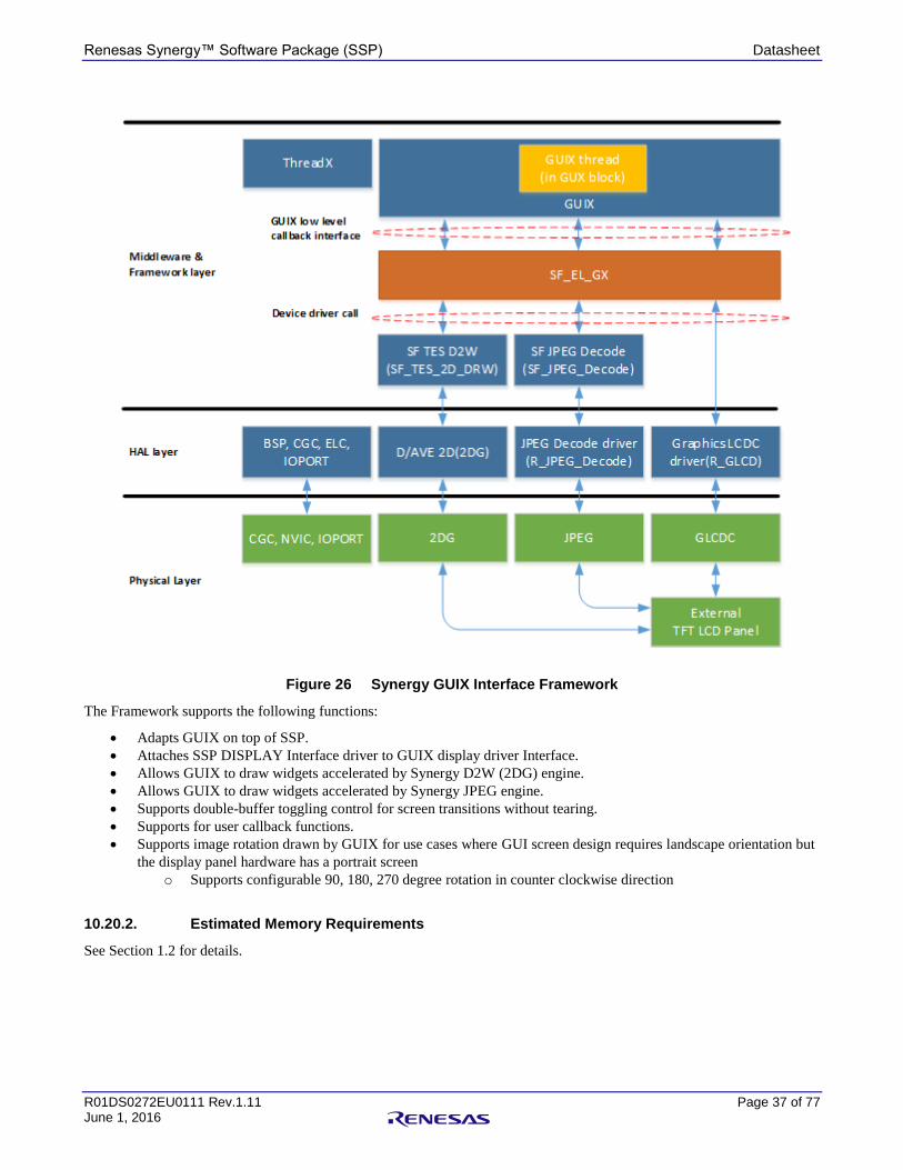
Renesas Synergy™ Software Package (SSP) Datasheet
R01DS0272EU0111 Rev.1.11 Page 37 of 77 June 1, 2016
Figure 26 Synergy GUIX Interface Framework
The Framework supports the following functions:
Adapts GUIX on top of SSP.
Attaches SSP DISPLAY Interface driver to GUIX display driver Interface.
Allows GUIX to draw widgets accelerated by Synergy D2W (2DG) engine.
Allows GUIX to draw widgets accelerated by Synergy JPEG engine.
Supports double-buffer toggling control for screen transitions without tearing.
Supports for user callback functions.
Supports image rotation drawn by GUIX for use cases where GUI screen design requires landscape orientation but
the display panel hardware has a portrait screen
o Supports configurable 90, 180, 270 degree rotation in counter clockwise direction
10.20.2. Estimated Memory Requirements
See Section 1.2 for details.
Renesas Synergy™ Software Package (SSP) Datasheet
R01DS0272EU0111 Rev.1.11 Page 38 of 77 June 1, 2016
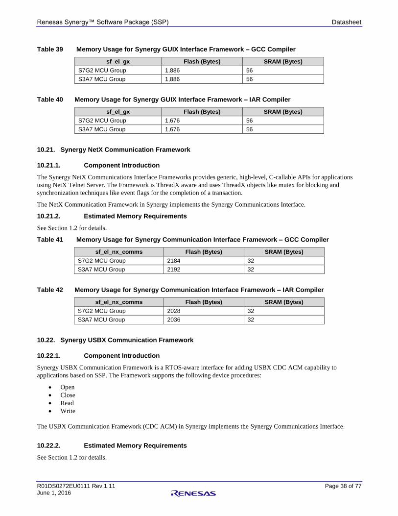
Table 39 Memory Usage for Synergy GUIX Interface Framework – GCC Compiler
sf_el_gx Flash (Bytes) SRAM (Bytes)
S7G2 MCU Group 1,886 56
S3A7 MCU Group 1,886 56
Table 40 Memory Usage for Synergy GUIX Interface Framework – IAR Compiler
sf_el_gx Flash (Bytes) SRAM (Bytes)
S7G2 MCU Group 1,676 56
S3A7 MCU Group 1,676 56
10.21. Synergy NetX Communication Framework
10.21.1. Component Introduction
The Synergy NetX Communications Interface Frameworks provides generic, high-level, C-callable APIs for applications
using NetX Telnet Server. The Framework is ThreadX aware and uses ThreadX objects like mutex for blocking and
synchronization techniques like event flags for the completion of a transaction.
The NetX Communication Framework in Synergy implements the Synergy Communications Interface.
10.21.2. Estimated Memory Requirements
See Section 1.2 for details.
Table 41 Memory Usage for Synergy Communication Interface Framework – GCC Compiler
sf_el_nx_comms Flash (Bytes) SRAM (Bytes)
S7G2 MCU Group 2184 32
S3A7 MCU Group 2192 32
Table 42 Memory Usage for Synergy Communication Interface Framework – IAR Compiler
sf_el_nx_comms Flash (Bytes) SRAM (Bytes)
S7G2 MCU Group 2028 32
S3A7 MCU Group 2036 32
10.22. Synergy USBX Communication Framework
10.22.1. Component Introduction
Synergy USBX Communication Framework is a RTOS-aware interface for adding USBX CDC ACM capability to
applications based on SSP. The Framework supports the following device procedures:
Open
Close
Read
Write
The USBX Communication Framework (CDC ACM) in Synergy implements the Synergy Communications Interface.
10.22.2. Estimated Memory Requirements
See Section 1.2 for details.

Renesas Synergy™ Software Package (SSP) Datasheet
R01DS0272EU0111 Rev.1.11 Page 39 of 77 June 1, 2016
Table 43 Memory Usage for Synergy USBX Communication Framework – GCC Compiler
sf_el_ux_comms Flash (Bytes) SRAM (Bytes)
S7G2 MCU Group 1,470 277
S3A7 MCU Group 1,470 277
S124 MCU Group 1,506 277
Table 44 Memory Usage for Synergy USBX Communication Framework – IAR Compiler
sf_el_ux_comms Flash (Bytes) SRAM (Bytes)
S7G2 MCU Group 1,288 284
S3A7 MCU Group 1,288 284
S124 MCU Group 1,328 284
10.23. Block Media Interface for SD Multi Media Card
10.23.1. Component Introduction
The Framework Block Media Interface is an abstract interface using function pointers instead of direct function calls.
Functions are called between FileX and the Synergy block media drivers, such as SDMMC and SPI Flash. The interface
remains the same for any media driver so that all media drivers appear functionally identical at file I/O layer and can be
interchanged with one another without changing code.
Device adaptation drivers, such as r_block_media_sdmmc, are accessed through the Block Media Interface and provide
device specific code needed to perform media I/O operations. Configuration and control structures passed through block
media function calls are generally device specific as well.
Figure 27 Block Media Interface for SD Multi Media Card
10.23.2. Estimated Memory Requirements
See Section 1.2 for details.

Renesas Synergy™ Software Package (SSP) Datasheet
R01DS0272EU0111 Rev.1.11 Page 40 of 77 June 1, 2016
Table 45 Memory Usage for Block Media Interface for SD Multi Media Card – GCC Compiler
sf_block_media_sdmmc Flash (Bytes) SRAM (Bytes)
S7G2 MCU Group 383 0
S3A7 MCU Group 383 0
Table 46 Memory Usage for Block Media Interface for SD Multi Media Card – IAR Compiler
sf_block_media_sdmmc Flash (Bytes) SRAM (Bytes)
S7G2 MCU Group 388 0
S3A7 MCU Group 388 0
11. Crypto Library
11.1. Component Introduction
The Secure Crypto Engine (SCE7) is the security and encryption block on Synergy S7G2 group MCUs. It features many
security features and National Institute of Standards and Technology (NIST)-compliant, primitive cryptographic algorithms
for various applications. These features and algorithms can perform authentication and secure communication between the
microcontroller and an external communication device or network, and can encrypt confidential and sensitive data and
program for storage in the microcontroller. The security and encryption block also features high-throughput and low-power
hardware accelerators to enable authentication and to meet secure communication requirements for various applications.
The SSP Cryptographic library provides a simple C-callable API interface for these functions and capabilities available in
the SCE7.
The SCE7 incorporates a high-throughput, 128-bit true random number generator (TRNG) that can generate random
numbers with high entropy for use as seeds to deterministic random number generators (such as NIST SP800-90A DRBG).
The TRNG generates cryptographically secure random numbers. Synergy MCUs also support several cryptographic hashing
functions SHA1/SHA224/SHA256/MD5/GHASH.
Additionally, SCE7 supports several NIST-compliant symmetric encryption algorithms like Advanced Encryption Standard
(AES 128/192/256-bit), Data Encryption Standard (3DES/DES) and Alleged RC4 (ARC4). These encryption algorithms,
along with private keys, are used for secure data exchange and to securely store data and program in the MCU.
SCE7 also supports several NIST-compliant asymmetric algorithms for data exchange. The data transmitter and receiver
uses shared keys.
The SSP Cryptographic library provides high-level, C-callable APIs for the following security functions in SCE7:
True RNG (TRNG).
Generates cryptographically secure 128-bit random numbers.
Generates seeds to other, deterministic random number generators (such as the NIST SP800-90A DRBG)
Cryptographic HASH functions.
Generates hash values that provide a digital fingerprint of data.
Supports SHA1 and SHA224/SHA256.
Encryption mechanism used for symmetric-key cryptography:
Encryption/decryption key is secretly shared between transmitter and receiver.
Advanced Encryption Standard (AES).
Supports 128-bit, 192-bit, and 256-bit key lengths.
Supports various chaining modes: ECB, CBC, CTR, GCM, and XTS.
Data Encryption Standard 3DES.
Supports 192-bit key length, operates on a fixed 8-byte block of data.
Supports ECB and CBC chaining modes.
Used in legacy secure socket layer (SSL) and transport layer security (TLS) protocols.

Renesas Synergy™ Software Package (SSP) Datasheet
R01DS0272EU0111 Rev.1.11 Page 41 of 77 June 1, 2016
3DES applies DES three times to each block.
Alleged RC4 (ARC4).
Supports 2048-bit key length.
Used in TLS and wired equivalent privacy (WEP).
Throughput for 128-bit data.
Encryption mechanism used for asymmetric-key cryptography:
Public keys are exchanged between the transmitter and receiver, then the public and private keys are used to
compute the shared secret between transmitter and receiver.
Rivest, Shamir, and Adleman (RSA).
Used for public-key cryptography.
Generates two keys: public and private.
Transmitter encrypts using the public key.
Receiver decrypts using the private key.
Supports up to 2048-bit key length.
Used in digital verification for authentication, signature generation and verification, encryption/decryption for key
exchange and wrapping, and other security functions.
11.2. Estimated Memory Requirements
See Section 1.2 for details.
Estimated memory requirements for this section will be provided in future updates of this document.
12. CMSIS DSP Library
12.1. Component Introduction
The ARM Cortex® Microcontroller Software Interface Standard DSP hardware block (CMSIS-DSP) in the Cortex®-M4
processor core-based Synergy family of MCUs provides a suite of common signal processing functions.
The CMSIS-DSP library is a hardware abstraction layer included in SSP for Synergy MCUs that includes a collection of
over 60 completely optimized signal processing functions commonly used in digital signal control applications. The library
supports key arithmetic formats such as fixed-point/fractional (Q7, Q15, Q31) and single precision floating-point (32-bit)
arithmetic for DSP operations. The combination of high-efficiency signal processing functions in SSP with the low-power,
low-cost, and high-performance benefits of Synergy MCUs having underlying SIMD architecture and FPU provide a
compelling solution for diverse applications in IoT/M2M markets.
The CMSIS-DSP library covers operations under the following major categories:
Basic math functions
Fast math functions
Complex math functions
Filters
Convolution
Matrix functions
Transforms
Motor control functions
Statistical functions
Support functions
Interpolation functions

Renesas Synergy™ Software Package (SSP) Datasheet
R01DS0272EU0111 Rev.1.11 Page 42 of 77 June 1, 2016
13. Hardware Abstraction Layer (HAL) Modules
13.1. Introduction
HAL modules in SSP are device-independent drivers for peripherals available on Synergy MCUs. The HAL modules
provide abstracted and well-defined interfaces. The underlying functionality of these interfaces can be implemented by
multiple device drivers. The HAL drivers use system services like timers and provide generic, high-level, C-callable
interfaces which are functional but device independent. The Application Framework in SSP uses the HAL drivers for
interfacing with the low-level device-specific drivers. HAL drivers can also be used by application programs to interface
directly with the respective peripheral, bypassing the SSP Framework. However these modules are RTOS independent (not
ThreadX aware) and are not thread-safe.
Figure 28 Hardware Abstraction Layer
13.2. SD Multi Media Card (SDMMC)
13.2.1. Component Introduction
The SDMMC driver module is a used access SD and a MMC memory device, including eMMC, on Synergy MCUs. The
driver implements the SD/MMC bus protocol for read, write, and control of SD cards and eMMC embedded devices
through the SDHI (SD Host Interface) peripheral. The SDMMC module can be used for standalone a SD card, eMMC,
media driver, or it can be used with FileX, or any other compatible file system. The SDMMC module can also be used as a
standalone SDIO card driver.
Specifications and Features supported by module:
Multiple channels of SD/MMC Host Interface SDHI.
SDSC (SD Standard Capacity), SDHC (SD High Capacity) and eMMC (embedded) modes.
1, 4 or 8 bit (eMMC only) data bus.
The Block Media Driver supports the SDMMC peripheral on the Synergy microcontroller hardware.
The SDMMC module implements the SDMMC interface in SSP.
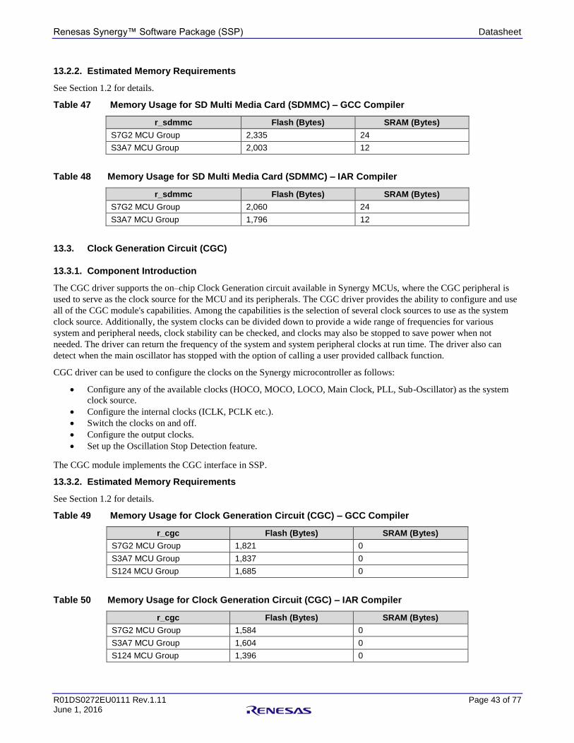
Renesas Synergy™ Software Package (SSP) Datasheet
R01DS0272EU0111 Rev.1.11 Page 43 of 77 June 1, 2016
13.2.2. Estimated Memory Requirements
See Section 1.2 for details.
Table 47 Memory Usage for SD Multi Media Card (SDMMC) – GCC Compiler
r_sdmmc Flash (Bytes) SRAM (Bytes)
S7G2 MCU Group 2,335 24
S3A7 MCU Group 2,003 12
Table 48 Memory Usage for SD Multi Media Card (SDMMC) – IAR Compiler
r_sdmmc Flash (Bytes) SRAM (Bytes)
S7G2 MCU Group 2,060 24
S3A7 MCU Group 1,796 12
13.3. Clock Generation Circuit (CGC)
13.3.1. Component Introduction
The CGC driver supports the on–chip Clock Generation circuit available in Synergy MCUs, where the CGC peripheral is
used to serve as the clock source for the MCU and its peripherals. The CGC driver provides the ability to configure and use
all of the CGC module's capabilities. Among the capabilities is the selection of several clock sources to use as the system
clock source. Additionally, the system clocks can be divided down to provide a wide range of frequencies for various
system and peripheral needs, clock stability can be checked, and clocks may also be stopped to save power when not
needed. The driver can return the frequency of the system and system peripheral clocks at run time. The driver also can
detect when the main oscillator has stopped with the option of calling a user provided callback function.
CGC driver can be used to configure the clocks on the Synergy microcontroller as follows:
Configure any of the available clocks (HOCO, MOCO, LOCO, Main Clock, PLL, Sub-Oscillator) as the system
clock source.
Configure the internal clocks (ICLK, PCLK etc.).
Switch the clocks on and off.
Configure the output clocks.
Set up the Oscillation Stop Detection feature.
The CGC module implements the CGC interface in SSP.
13.3.2. Estimated Memory Requirements
See Section 1.2 for details.
Table 49 Memory Usage for Clock Generation Circuit (CGC) – GCC Compiler
r_cgc Flash (Bytes) SRAM (Bytes)
S7G2 MCU Group 1,821 0
S3A7 MCU Group 1,837 0
S124 MCU Group 1,685 0
Table 50 Memory Usage for Clock Generation Circuit (CGC) – IAR Compiler
r_cgc Flash (Bytes) SRAM (Bytes)
S7G2 MCU Group 1,584 0
S3A7 MCU Group 1,604 0
S124 MCU Group 1,396 0

Renesas Synergy™ Software Package (SSP) Datasheet
R01DS0272EU0111 Rev.1.11 Page 44 of 77 June 1, 2016
13.4. Capacitive Touch Sensing Unit (CTSU)
13.4.1. Component Introduction
The Capacitive Touch Sensing Unit (CTSU) driver supports the CTSU peripheral on the Synergy Microcontrollers. The
CTSU driver provides the functionality necessary to open, close, run and control the CTSU peripheral depending upon the
configuration passed as arguments. The CTSU HAL driver is used to initialize the CTSU peripheral to detect a change in
capacitance on any of the configured (and enabled) channels, perform requisite filtering, and generate a variety of data that
can be used by higher level framework layers like buttons, wheels, and sliders. To support the different types of data
required by these layers, the implementation provides a function that allows upper level layers to read different types of
processed data based on their need. The driver will scan the configured channels, move data using the DTC, perform
filtering, drift compensation, auto-tuning and notify the user via a callback once each iteration is completed and new
processing data is available. These callbacks can be used by upper layers to read the data.
This module has been designed to be used together with the Workbench 6 tool which generates the required structures for
initialization and operation. The driver also allows the user to provide their own filtering and auto-tuning algorithms and
integrate it into the process. The driver can only support one configuration at a time, but the user can reopen the driver with
multiple channel configurations as required by the application.
The CTSU driver allows the user to configure the CTSU channels for all the supported operation modes including Mutual
and Self Capacitance.
The CTSU driver implements the CTSU interface in SSP.
13.4.2. Estimated Memory Requirements
See Section 1.2 for details.
Table 51 Memory Usage for Capacitive Touch Sensing Unit (CTSU) – GCC Compiler
r_ctsu Flash (Bytes) SRAM (Bytes)
S7G2 MCU Group 13,276 916
S3A7 MCU Group 13,512 916
S124 MCU Group 13,400 916
Table 52 Memory Usage for Capacitive Touch Sensing Unit (CTSU) – IAR Compiler
r_ctsu Flash (Bytes) SRAM (Bytes)
S7G2 MCU Group 11,908 1,220
S3A7 MCU Group 12,040 1,220
S124 MCU Group 12,388 1,220
13.5. Digital to Analog convertor (DAC)
13.5.1. Component Introduction
The DAC module in SSP supports the 12-bit D/A converter in Synergy MCUs. This driver configures the dual-channel 12-
bit D/A Converter (DAC12) to output one of 4096 voltage levels between the positive and negative reference voltages.
Key features supported by module include:
Set left-justified or right-justified 12-bit value format for 16-bit input data registers.
Enable or disable output amplifiers.
Select external or internal reference voltages.
Operate in synchronous anti-interference mode with Analog-to-Digital Converter (ADC) Module.
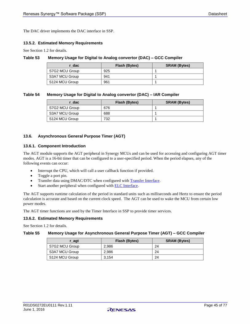
Renesas Synergy™ Software Package (SSP) Datasheet
R01DS0272EU0111 Rev.1.11 Page 45 of 77 June 1, 2016
The DAC driver implements the DAC interface in SSP.
13.5.2. Estimated Memory Requirements
See Section 1.2 for details.
Table 53 Memory Usage for Digital to Analog convertor (DAC) – GCC Compiler
r_dac Flash (Bytes) SRAM (Bytes)
S7G2 MCU Group 925 1
S3A7 MCU Group 941 1
S124 MCU Group 961 1
Table 54 Memory Usage for Digital to Analog convertor (DAC) – IAR Compiler
r_dac Flash (Bytes) SRAM (Bytes)
S7G2 MCU Group 676 1
S3A7 MCU Group 688 1
S124 MCU Group 732 1
13.6. Asynchronous General Purpose Timer (AGT)
13.6.1. Component Introduction
The AGT module supports the AGT peripheral in Synergy MCUs and can be used for accessing and configuring AGT timer
modes. AGT is a 16-bit timer that can be configured to a user-specified period. When the period elapses, any of the
following events can occur:
Interrupt the CPU, which will call a user callback function if provided.
Toggle a port pin.
Transfer data using DMAC/DTC when configured with Transfer Interface.
Start another peripheral when configured with ELC Interface.
The AGT supports runtime calculation of the period in standard units such as milliseconds and Hertz to ensure the period
calculation is accurate and based on the current clock speed. The AGT can be used to wake the MCU from certain low
power modes.
The AGT timer functions are used by the Timer Interface in SSP to provide timer services.
13.6.2. Estimated Memory Requirements
See Section 1.2 for details.
Table 55 Memory Usage for Asynchronous General Purpose Timer (AGT) – GCC Compiler
r_agt Flash (Bytes) SRAM (Bytes)
S7G2 MCU Group 2,986 24
S3A7 MCU Group 2,986 24
S124 MCU Group 3,154 24

Renesas Synergy™ Software Package (SSP) Datasheet
R01DS0272EU0111 Rev.1.11 Page 46 of 77 June 1, 2016
Table 56 Memory Usage for Asynchronous General Purpose Timer (AGT) – IAR Compiler
r_agt Flash (Bytes) SRAM (Bytes)
S7G2 MCU Group 2,552 32
S3A7 MCU Group 2,552 32
S124 MCU Group 2,682 32
13.7. Cyclic Redundancy Check calculator (CRC)
13.7.1. Component Introduction
The CRC HAL driver supports the CRC hardware block in Synergy MCUs that can be used to calculate 8, 16, and 32 bit
CRC values on a block of data in memory or a stream of data over a serial port using various types of industry standard
polynomials. CRC calculations can be performed by sending data to the block using the CPU or by snooping on read or
write activity on one of 10 SCI channels.
The CRC module supports the following functions:
Calculate a CRC on a block of data in memory.
Calculate a CRC on a stream of data being transmitted or received over a serial port.
Specify the number of the serial port and the direction of data to perform the calculation on.
The CRC driver implements the CRC interface in SSP.
13.7.2. Estimated Memory Requirements
See Section 1.2 for details.
Table 57 Memory Usage for Cyclic Redundancy Check calculator (CRC) – GCC Compiler
r_crc Flash (Bytes) SRAM (Bytes)
S7G2 MCU Group 817 0
S3A7 MCU Group 817 0
S124 MCU Group 913 0
Table 58 Memory Usage for Cyclic Redundancy Check calculator (CRC) – IAR Compiler
r_crc Flash (Bytes) SRAM (Bytes)
S7G2 MCU Group 552 0
S3A7 MCU Group 552 0
S124 MCU Group 624 0
13.8. Clock Frequency Accuracy Measurement (CAC)
13.8.1. Component Introduction
The CAC (Clock Accuracy Circuit) driver supports the clock frequency measurement circuit capable of monitoring the
clock frequency based on a reference signal input. The reference signal may be an externally supplied clock source, or one
of several available internal clock sources. An interrupt request may optionally be generated by a completed measurement, a
detected frequency error, or a counter overflow. A digital filter is available for an externally supplied reference clock, and
dividers are available for both internally supplied measurement and reference clocks. Edge detection options for the
reference clock are configurable as rising, falling or both edges.
The frequency of the following clocks can be measured:
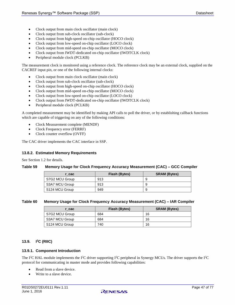
Renesas Synergy™ Software Package (SSP) Datasheet
R01DS0272EU0111 Rev.1.11 Page 47 of 77 June 1, 2016
Clock output from main clock oscillator (main clock)
Clock output from sub-clock oscillator (sub-clock)
Clock output from high-speed on-chip oscillator (HOCO clock)
Clock output from low-speed on-chip oscillator (LOCO clock)
Clock output from mid-speed on-chip oscillator (MOCO clock)
Clock output from IWDT-dedicated on-chip oscillator (IWDTCLK clock)
Peripheral module clock (PCLKB)
The measurement clock is monitored using a reference clock. The reference clock may be an external clock, supplied on the
CACREF input pin, or one of the following internal clocks:
Clock output from main clock oscillator (main clock)
Clock output from sub-clock oscillator (sub-clock)
Clock output from high-speed on-chip oscillator (HOCO clock)
Clock output from mid-speed on-chip oscillator (MOCO clock)
Clock output from low-speed on-chip oscillator (LOCO clock)
Clock output from IWDT-dedicated on-chip oscillator (IWDTCLK clock)
Peripheral module clock (PCLKB)
A completed measurement may be identified by making API calls to poll the driver, or by establishing callback functions
which are capable of triggering on any of the following conditions:
Clock Measurement complete (MENDF)
Clock Frequency error (FERRF)
Clock counter overflow (OVFF)
The CAC driver implements the CAC interface in SSP.
13.8.2. Estimated Memory Requirements
See Section 1.2 for details.
Table 59 Memory Usage for Clock Frequency Accuracy Measurement (CAC) – GCC Compiler
r_cac Flash (Bytes) SRAM (Bytes)
S7G2 MCU Group 913 9
S3A7 MCU Group 913 9
S124 MCU Group 949 9
Table 60 Memory Usage for Clock Frequency Accuracy Measurement (CAC) – IAR Compiler
r_cac Flash (Bytes) SRAM (Bytes)
S7G2 MCU Group 684 16
S3A7 MCU Group 684 16
S124 MCU Group 740 16
13.9. I2C (RIIC)
13.9.1. Component Introduction
The I2C HAL module implements the I2C driver supporting I2C peripheral in Synergy MCUs. The driver supports the I2C
protocol for communicating in master mode and provides following capabilities:
Read from a slave device.
Write to a slave device.

Renesas Synergy™ Software Package (SSP) Datasheet
R01DS0272EU0111 Rev.1.11 Page 48 of 77 June 1, 2016
Reset the I2C peripheral.
Interrupt driven transmit/receive processing.
Callback function support which can return an event code.
Supports I2C Fast-mode with bit rates of up to 400 kHz.
Supports Fast-mode plus with 1 MHz bit rates.
The callback functions will be called with the following events:
Transfer aborted
Transmit complete
Receive complete
The callback structure provides the number of bytes that were sent or received.
SCI_I2C and I2C HAL drivers implements the I2C interface in SSP.
13.9.2. Estimated Memory Requirements
See Section 1.2 for details.
Table 61 Memory Usage for I2C (RIIC) – GCC Compiler
r_riic Flash (Bytes) SRAM (Bytes)
S7G2 MCU Group 8,569 132
S3A7 MCU Group 8,569 132
S124 MCU Group 7,008 131
Table 62 Memory Usage for I2C (RIIC) – IAR Compiler
r_riic Flash (Bytes) SRAM (Bytes)
S7G2 MCU Group 3,864 136
S3A7 MCU Group 3,864 136
S124 MCU Group 3,780 136
13.10. Serial Peripheral Interface (RSPI)
13.10.1. Component Introduction
The SPI HAL driver supports the SPI interface in Synergy MCUs and implements the SPI protocol.
The SPI driver configures SPI peripheral in master mode and supports the following functions:
Initialize the driver.
Serial Communication through SPI operation.
Supports 8, 16 and 32 bit data transfers.
Supports GPIO pins configured as chip selects.
The Interface also provides support for callbacks. The callback functions are called with the following events:
Transfer aborted
Transfer complete
Mode fault
Error events
The SPI HAL Interface is implemented by the SCI_SPI and SPI HAL driver modules in SSP.
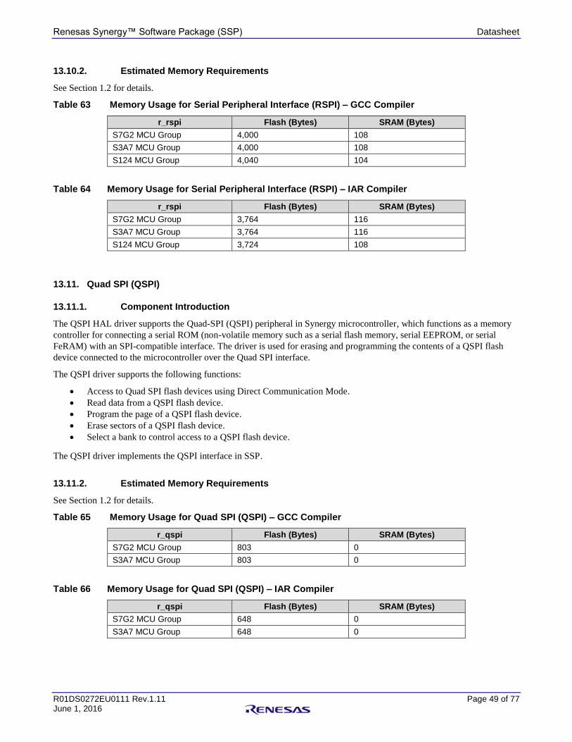
Renesas Synergy™ Software Package (SSP) Datasheet
R01DS0272EU0111 Rev.1.11 Page 49 of 77 June 1, 2016
13.10.2. Estimated Memory Requirements
See Section 1.2 for details.
Table 63 Memory Usage for Serial Peripheral Interface (RSPI) – GCC Compiler
r_rspi Flash (Bytes) SRAM (Bytes)
S7G2 MCU Group 4,000 108
S3A7 MCU Group 4,000 108
S124 MCU Group 4,040 104
Table 64 Memory Usage for Serial Peripheral Interface (RSPI) – IAR Compiler
r_rspi Flash (Bytes) SRAM (Bytes)
S7G2 MCU Group 3,764 116
S3A7 MCU Group 3,764 116
S124 MCU Group 3,724 108
13.11. Quad SPI (QSPI)
13.11.1. Component Introduction
The QSPI HAL driver supports the Quad-SPI (QSPI) peripheral in Synergy microcontroller, which functions as a memory
controller for connecting a serial ROM (non-volatile memory such as a serial flash memory, serial EEPROM, or serial
FeRAM) with an SPI-compatible interface. The driver is used for erasing and programming the contents of a QSPI flash
device connected to the microcontroller over the Quad SPI interface.
The QSPI driver supports the following functions:
Access to Quad SPI flash devices using Direct Communication Mode.
Read data from a QSPI flash device.
Program the page of a QSPI flash device.
Erase sectors of a QSPI flash device.
Select a bank to control access to a QSPI flash device.
The QSPI driver implements the QSPI interface in SSP.
13.11.2. Estimated Memory Requirements
See Section 1.2 for details.
Table 65 Memory Usage for Quad SPI (QSPI) – GCC Compiler
r_qspi Flash (Bytes) SRAM (Bytes)
S7G2 MCU Group 803 0
S3A7 MCU Group 803 0
Table 66 Memory Usage for Quad SPI (QSPI) – IAR Compiler
r_qspi Flash (Bytes) SRAM (Bytes)
S7G2 MCU Group 648 0
S3A7 MCU Group 648 0

Renesas Synergy™ Software Package (SSP) Datasheet
R01DS0272EU0111 Rev.1.11 Page 50 of 77 June 1, 2016
13.12. Realtime clock (RTC)
13.12.1. Component Introduction
The RTC HAL driver controls the Realtime Clock. The driver supports the RTC peripheral available on the Synergy
microcontroller hardware.
The RTC driver supports the following functions of the Realtime Clock:
RTC peripheral configuration
Clock and calendar functions
Alarm, periodic, and carry interrupts
Time capture function
Event linkage to other peripherals
The RTC driver implements the RTC interface in SSP.
13.12.2. Estimated Memory Requirements
See Section 1.2 for details.
Table 67 Memory Usage for Realtime clock (RTC) – GCC Compiler
r_rtc Flash (Bytes) SRAM (Bytes)
S7G2 MCU Group 2,669 20
S3A7 MCU Group 2,669 20
S124 MCU Group 2,849 20
Table 68 Memory Usage for Realtime clock (RTC) – IAR Compiler
r_rtc Flash (Bytes) SRAM (Bytes)
S7G2 MCU Group 2,084 20
S3A7 MCU Group 2,084 20
S124 MCU Group 2,284 20
13.13. Segment LCD (SLCDC)
13.13.1. Component Introduction
The Segment LCD HAL driver controls the Segment LCD Display. The driver supports the SLCD peripheral available on
the Synergy microcontroller hardware.
The driver uses the Segment LCD controller (SLCDC) to display data on a Segment LCD. The driver initializes the LCD
for displaying data and configures the drive voltage generator, the display waveform, number of time slices, and the bias
methods to drive the LCD. This module provides functions to display data to a specified set of segments, to update existing
segment data, to enable and disable display, to set the display area, and to adjust the contrast.
Module supports selecting the following features:
Internal voltage boosting for the LCD driver voltage generator: Select the capacitor split method or the external
resistance division.
Display bias: Select the 1/2 bias method, 1/3 bias method, or 1/4 bias method.
Time slice of the display: Select static, 2-time slice, 3-time slice, 4-time slice, or 8-time slice.
Display waveform: Select waveform A or waveform B.
Display data area: Select A-pattern, B-pattern, or blinking. You can switch the display data area.
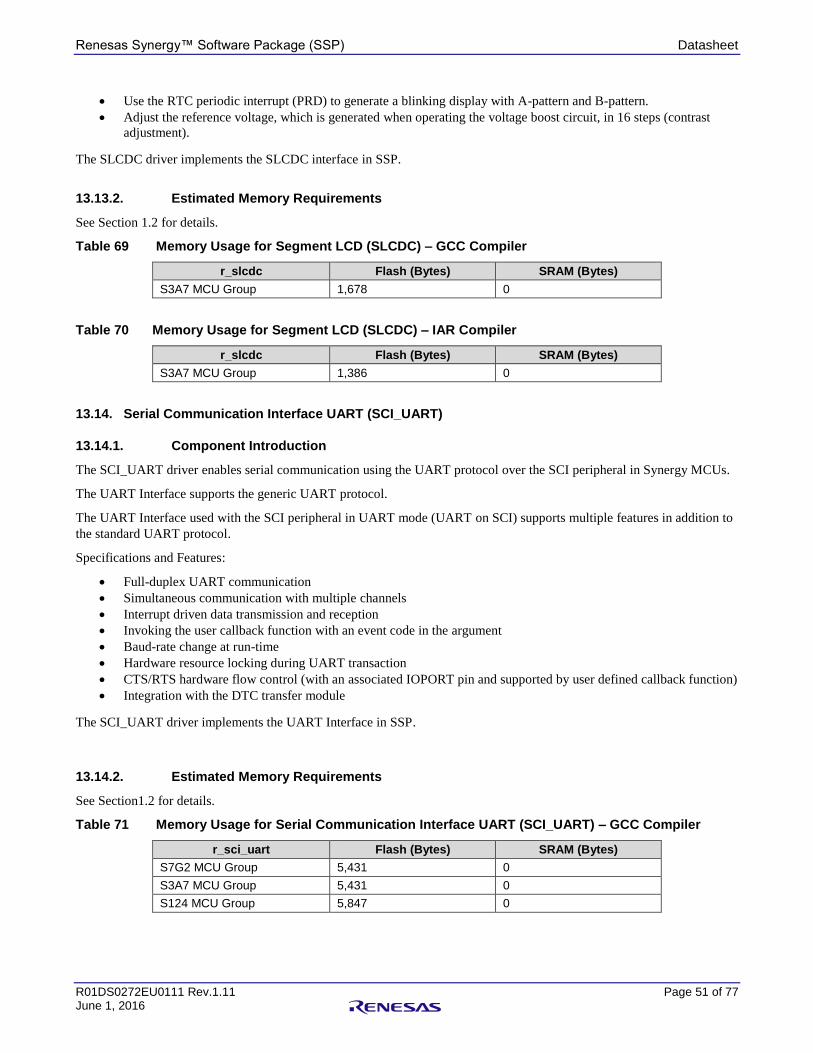
Renesas Synergy™ Software Package (SSP) Datasheet
R01DS0272EU0111 Rev.1.11 Page 51 of 77 June 1, 2016
Use the RTC periodic interrupt (PRD) to generate a blinking display with A-pattern and B-pattern.
Adjust the reference voltage, which is generated when operating the voltage boost circuit, in 16 steps (contrast
adjustment).
The SLCDC driver implements the SLCDC interface in SSP.
13.13.2. Estimated Memory Requirements
See Section 1.2 for details.
Table 69 Memory Usage for Segment LCD (SLCDC) – GCC Compiler
r_slcdc Flash (Bytes) SRAM (Bytes)
S3A7 MCU Group 1,678 0
Table 70 Memory Usage for Segment LCD (SLCDC) – IAR Compiler
r_slcdc Flash (Bytes) SRAM (Bytes)
S3A7 MCU Group 1,386 0
13.14. Serial Communication Interface UART (SCI_UART)
13.14.1. Component Introduction
The SCI_UART driver enables serial communication using the UART protocol over the SCI peripheral in Synergy MCUs.
The UART Interface supports the generic UART protocol.
The UART Interface used with the SCI peripheral in UART mode (UART on SCI) supports multiple features in addition to
the standard UART protocol.
Specifications and Features:
Full-duplex UART communication
Simultaneous communication with multiple channels
Interrupt driven data transmission and reception
Invoking the user callback function with an event code in the argument
Baud-rate change at run-time
Hardware resource locking during UART transaction
CTS/RTS hardware flow control (with an associated IOPORT pin and supported by user defined callback function)
Integration with the DTC transfer module
The SCI_UART driver implements the UART Interface in SSP.
13.14.2. Estimated Memory Requirements
See Section1.2 for details.
Table 71 Memory Usage for Serial Communication Interface UART (SCI_UART) – GCC Compiler
r_sci_uart Flash (Bytes) SRAM (Bytes)
S7G2 MCU Group 5,431 0
S3A7 MCU Group 5,431 0
S124 MCU Group 5,847 0

Renesas Synergy™ Software Package (SSP) Datasheet
R01DS0272EU0111 Rev.1.11 Page 52 of 77 June 1, 2016
Table 72 Memory Usage for Serial Communication Interface UART (SCI_UART) – IAR Compiler
r_sci_uart Flash (Bytes) SRAM (Bytes)
S7G2 MCU Group 4,176 40
S3A7 MCU Group 4,176 40
S124 MCU Group 4,768 24
13.15. Serial Communication Interface I2C (SCI_I2C)
13.15.1. Component Introduction
The SCI_I2C driver supports the SCI peripheral in Synergy MCUs. The driver supports the I2C protocol for communicating
in master mode and provides following capabilities:
Read from a slave device.
Write to a slave device.
Reset the I2C peripheral.
Interrupt driven transmit/receive processing.
Callback function support which can return an event code.
Supports I2C Fast-mode with bit rates of up to 400 kHz.
The callback functions will be called with the following events:
Transfer aborted
Transmit complete
Receive complete
The callback structure provides the number of bytes that were sent or received.
The I2C on SCI driver implements the I2C interface in SSP.
13.15.2. Estimated Memory Requirements
See Section 1.2 for details.
Table 73 Memory Usage for Serial Communication Interface I2C (SCI_I2C) – GCC Compiler
r_sci_i2c Flash (Bytes) SRAM (Bytes)
S7G2 MCU Group 4,133 400
S3A7 MCU Group 3,853 400
S124 MCU Group 3,773 400
Table 74 Memory Usage for Serial Communication Interface I2C (SCI_I2C) – IAR Compiler
r_sci_i2c Flash (Bytes) SRAM (Bytes)
S7G2 MCU Group 2,868 400
S3A7 MCU Group 2,924 400
S124 MCU Group 3,032 400

Renesas Synergy™ Software Package (SSP) Datasheet
R01DS0272EU0111 Rev.1.11 Page 53 of 77 June 1, 2016
13.16. Serial Communication Interface SPI (SCI_SPI)
13.16.1. Component Introduction
SCI_SPI HAL driver module supports SPI serial communication using the microcontroller's SCI peripheral. The module
implements the SPI Interface. The SPI Interface configures SPI communication in master mode. The Interface allows:
Initializing the driver
Serial Communication through SPI operation
The Interface also provides support for callbacks. The callback functions are called with the following events:
Transfer aborted
Transfer complete
Mode fault
Error events
Selecting a SPI Module
SCI_SPI module support 8-bit data transfer and GPIO pins configured as chip selects. The module uses DTC for data
transfer.
The SPI HAL Interface is implemented by the SCI_SPI HAL driver modules in SSP.
13.16.2. Estimated Memory Requirements
See Section 1.2 for details.
Table 75 Memory Usage for Serial Communication Interface SPI (SCI_SPI) – GCC Compiler
r_sci_spi Flash (Bytes) SRAM (Bytes)
S7G2 MCU Group 5,671 440
S3A7 MCU Group 5,015 440
S124 MCU Group 4,079 440
Table 76 Memory Usage for Serial Communication Interface SPI (SCI_SPI) – IAR Compiler
r_sci_spi Flash (Bytes) SRAM (Bytes)
S7G2 MCU Group 3,096 480
S3A7 MCU Group 2,952 480
S124 MCU Group 3184 464
13.17. JPEG Codec (JPEG Codec)
13.17.1. Component Introduction
The on-chip JPEG engine performs high-speed image data compression and decoding of JPEG image data. The JPEG
Decoder conforms to the JPEG baseline decompression standard, JPEG Part 2, ISO-IEC10918-2. The JPEG Codec HAL
driver module supports the JPEG hardware peripheral in Synergy MCUs.
Specifications and Features:
Supports JPEG decompression for applications to convert a JPEG image into bitmap data suitable for display
frame buffer.
Supports polling mode that allows an application to wait for JPEG decoder to complete.
Supports Interrupt mode with user-supplied callback functions.

Renesas Synergy™ Software Package (SSP) Datasheet
R01DS0272EU0111 Rev.1.11 Page 54 of 77 June 1, 2016
Provides interfaces for applications to specify parameters such as:
o Horizontal and vertical subsample values
o Horizontal stride
o Decoded pixel format
o Input and output data format
o Color space.
Obtains the size of image prior to the decoding step.
Supports putting encoded data in an input buffer and an output buffer to store the decoded image frame.
Streams encoded data input into JPEG Decoder module. This feature allows an application to read encoded JPEG
image from a file or from network while decoding it, without the necessity to buffer the entire image.
Supports streaming coded data into JPEG Decoder module. This feature allows an application to read coded JPEG
image from a file or from network without buffering the entire image
Configures the number of image lines to decode. This feature enables the application to process the decoded image
on the fly without buffering the entire frame.
Supports the input decoded formats YCbCr444, YCbCr422, YCbCr420, YCbCr411.
Supports the output decoded formats ARGB8888 and RGB565.
Returns error when JPEG image’s size height and width do not match the specified input values.
The JPEG Codec HAL module implements the JPEG Decode interface in SSP.
13.17.2. Estimated Memory Requirements
See Section 1.2 for details.
Table 77 Memory Usage for JPEG Codec (JPEG Codec) – GCC Compiler
r_jpeg_decode Flash (Bytes) SRAM (Bytes)
S7G2 MCU Group 2,637 4
Table 78 Memory Usage for JPEG Codec (JPEG Codec) – IAR Compiler
r_jpeg_decode Flash (Bytes) SRAM (Bytes)
S7G2 MCU Group 2,304 4
13.18. Flash Memory-High Performance (FLASH_HP)
13.18.1. Component Introduction
The Flash memory module supports the following features:
The S7 Series microcontrollers support up to 4 MB high-speed Code flash for user applications and 64 KB of high-
speed Data Flash for storing data. The Flash Memory-High Performance HAL driver supports the High
Performance Flash memory block on S7 Series MCU and enables an application to read, write and erase both the
Data and ROM flash areas that reside within the MCU. The amount of flash memory available varies across MCU
parts, but the functionality available through the module is listed below: Blocking erasing, reading, writing and
blank checking of ROM flash.
Both blocking and non-blocking erasing, reading, writing and blank checking of Data and Code flash.
Callback functions for completion of non-blocking data flash operations.
Access window (write protection) for Rom flash allowing only specified areas of code flash to be erased or written.
Swap area for boot block swapping which allows safe re-writing of the startup program without first erasing it.
The driver makes the process of programming and erasing on-chip flash areas easy. The module can be used to perform
blocking erase and program operations for both code and data flash, with BGO operation available for data flash operations
only. When a code flash operation is on-going, you cannot access that code flash area. If there’s an attempt to access the
code flash area while a code Flash operation is in progress, the flash control unit will transition into an error state.
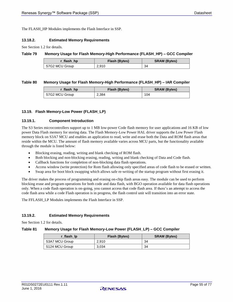
Renesas Synergy™ Software Package (SSP) Datasheet
R01DS0272EU0111 Rev.1.11 Page 55 of 77 June 1, 2016
The FLASH_HP Modules implements the Flash Interface in SSP.
13.18.2. Estimated Memory Requirements
See Section 1.2 for details.
Table 79 Memory Usage for Flash Memory-High Performance (FLASH_HP) – GCC Compiler
r_flash_hp Flash (Bytes) SRAM (Bytes)
S7G2 MCU Group 2,910 34
Table 80 Memory Usage for Flash Memory-High Performance (FLASH_HP) – IAR Compiler
r_flash_hp Flash (Bytes) SRAM (Bytes)
S7G2 MCU Group 2,384 104
13.19. Flash Memory-Low Power (FLASH_LP)
13.19.1. Component Introduction
The S3 Series microcontrollers support up to 1 MB low-power Code flash memory for user applications and 16 KB of low
power Data Flash memory for storing data. The Flash Memory-Low Power HAL driver supports the Low Power Flash
memory block on S3A7 MCU and enables an application to read, write and erase both the Data and ROM flash areas that
reside within the MCU. The amount of flash memory available varies across MCU parts, but the functionality available
through the module is listed below:
Blocking erasing, reading, writing and blank checking of ROM flash.
Both blocking and non-blocking erasing, reading, writing and blank checking of Data and Code flash.
Callback functions for completion of non-blocking data flash operations.
Access window (write protection) for Rom flash allowing only specified areas of code flash to be erased or written.
Swap area for boot block swapping which allows safe re-writing of the startup program without first erasing it.
The driver makes the process of programming and erasing on-chip flash areas easy. The module can be used to perform
blocking erase and program operations for both code and data flash, with BGO operation available for data flash operations
only. When a code flash operation is on-going, you cannot access that code flash area. If there’s an attempt to access the
code flash area while a code Flash operation is in progress, the flash control unit will transition into an error state.
The FFLASH_LP Modules implements the Flash Interface in SSP.
13.19.2. Estimated Memory Requirements
See Section 1.2 for details.
Table 81 Memory Usage for Flash Memory-Low Power (FLASH_LP) – GCC Compiler
r_flash_lp Flash (Bytes) SRAM (Bytes)
S3A7 MCU Group 2,910 34
S124 MCU Group 3,034 34
Renesas Synergy™ Software Package (SSP) Datasheet
R01DS0272EU0111 Rev.1.11 Page 56 of 77 June 1, 2016
Table 82 Memory Usage for Flash Memory-Low Power (FLASH_LP) – IAR Compiler
r_flash_lp Flash (Bytes) SRAM (Bytes)
S3A7 MCU Group 2,364 104
S124 MCU Group 2,464 104
13.20. Data Transfer Controller (DTC)
13.20.1. Component Introduction
Data Transfer Controller (DTC) driver supports the DTC peripheral that is used to transfer data between memory and
peripherals, or between two peripherals without CPU intervention (background data transfer). The DTC driver moves data
from a user specified source to a user specified destination when an interrupt or event occurs. The DTC module uses a RAM
based vector table, with slots for every interrupt in the system. When the DTC transfer completes, the activation source
interrupt is called. The activation source interrupt must be enabled to use the DTC. The activation source interrupt is
generally muted by the DTC until the transfer completes, unless TRANSFER_IRQ_EACH is specified in the configuration.
The DTC also allows chained transfers, meaning that more than one transfer can occur after a single activation source
interrupt. This feature is supported by the driver but must be configured outside the e2 studio IDE.
The Data Transfer Controller allows data transfers to occur in place of or in addition to any interrupt. It does not support
data transfers using software start.
The DTC module supports following transfer modes:
Normal Mode - A single transfer is triggered each time an activation source event occurs. A single transfer is 1
byte, 2 bytes, or 4 bytes depending on the selected settings. Total length (size) of data to be transferred is
configurable.
Repeat Mode – In addition to the length (size) of data block that needs to be transferred, Repeat Mode provides
additional provision for specifying number of time transfer should be repeated with the same length of data. In this
mode if the repeat area is set to source, the same source location is used for each transfer iteration. Alternatively, if
the repeat area is set to destination, the same destination location is used for each transfer iteration.
Block Mode – The block mode transfer operates similar to the Repeat mode, but is triggered by a source event, the
entire transfer length is transferred each time an activation source event occurs. For example, if a transfer is
configured in block mode with timer as the activation source, a 2 byte size, and a 12 byte length, 24 bytes are
transferred each time the activation source event occurs. Similar to Block Mode if the repeat area is set to source,
the source register is reloaded with its initial value when the transfer restarts.
Address Mode – The Address mode transfer operates similar to the Normal Mode, but after each transfer the
source pointer and destination pointer is incremented by the length of transfer
Chained Transfer Mode - Chained transfers are only supported by DTC, in this mode successive transfers are
linked by creating an array of Transfer Info structures and setting the mode
TRANSFER_CHAIN_MODE_ENABLED for all transfers except the last transfer. The module is configured to
point to the base of the first structure in the array to indicate the first transfer source and destination location.
The HAL Transfer Interface is a generic interface for Transfer applications and is implemented by two data transfer
modules in SSP, DMAC and DTC.
13.20.2. Estimated Memory Requirements
See Section 1.2 for details.

Renesas Synergy™ Software Package (SSP) Datasheet
R01DS0272EU0111 Rev.1.11 Page 57 of 77 June 1, 2016
Table 83 Memory Usage for Data Transfer Controller (DTC) – GCC Compiler
r_dtc Flash (Bytes) SRAM (Bytes)
S7G2 MCU Group 1,930 33
S3A7 MCU Group 1,930 33
S124 MCU Group 1,942 33
Table 84 Memory Usage for Data Transfer Controller (DTC) – IAR Compiler
r_dtc Flash (Bytes) SRAM (Bytes)
S7G2 MCU Group 1,566 38
S3A7 MCU Group 1,566 38
S124 MCU Group 1,586 38
13.21. Data Operation Circuit (DOC)
13.21.1. Component Introduction
The Data Operation Circuit (DOC) peripheral performs a 16-bit addition, subtraction, and comparison without CPU
intervention. The DOC driver provided with SSP supports the DOC peripheral available on the Synergy microcontroller
hardware and controls the peripheral according to user configuration.
The driver can detect the following events:
A mismatch or match between data values
Overflow of an addition operation
Underflow of a subtraction operation
When the configured event occurs and a callback is available (with interrupts enabled), the driver invokes the callback with
the supplied arguments, which in-turn indicates the occurrence of the event to application. If interrupts are not enabled, the
API supports checking the DOC status to poll the status of the comparison, addition or subtraction operation.
The DOC driver implements the DOC interface in SSP.
13.21.2. Estimated Memory Requirements
See Section 1.2 for details.
Table 85 Memory Usage for Data Operation Circuit (DOC) – GCC Compiler
r_doc Flash (Bytes) SRAM (Bytes)
S7G2 MCU Group 796 4
S3A7 MCU Group 796 4
S124 MCU Group 828 4
Table 86 Memory Usage for Data Operation Circuit (DOC) – IAR Compiler
r_doc Flash (Bytes) SRAM (Bytes)
S7G2 MCU Group 596 4
S3A7 MCU Group 596 4
S124 MCU Group 632 4

Renesas Synergy™ Software Package (SSP) Datasheet
R01DS0272EU0111 Rev.1.11 Page 58 of 77 June 1, 2016
13.22. Direct Memory Access Controller (DMAC)
13.22.1. Component Introduction
The Direct Memory Access Controller (DMAC) driver supports the DMAC peripheral that is used to transfer data between
memory and peripherals, or between two peripherals without CPU intervention (background data transfer). The DMAC
driver moves data from a user specified source to a user specified destination when an interrupt or event occurs. The DMAC
module uses DMAC peripheral registers, so the number of transfers in the system is limited to number of available DMAC
channels on the device. The activation source does not have to be enabled to use the DMAC. When the DMAC transfer
completes, a DMAC interrupt is called. If the activation source interrupt is enabled, it fires at the same time the transfer is
triggered. If the DMAC interrupt is enabled, it fires after all transfers are complete. The DMAC does not support chained
transfers.
The DMAC module supports following transfer modes:
Normal Mode – A single transfer is triggered each time an activation source event occurs. A single transfer is 1
byte, 2 bytes, or 4 bytes depending on the selected settings. Total length (size) of data to be transferred is
configurable.
Repeat Mode – In addition to the length (size) of data block that needs to be transferred, Repeat Mode provides
additional provision for specifying number of time transfer should be repeated with the same length of data. In this
mode if the repeat area is set to source, the same source location is used for each transfer iteration. Alternatively, if
the repeat area is set to destination, the same destination location is used for each transfer iteration.
Block Mode – The block mode transfer operates similar to the Repeat mode, but is triggered by a source event, the
entire transfer length is transferred each time an activation source event occurs. For example, if a transfer is
configured in block mode with timer as the activation source, a 2 byte size, and a 12 byte length, 24 bytes are
transferred each time the activation source event occurs. Similar to Block Mode if the repeat area is set to source,
the source register is reloaded with its initial value when the transfer restarts.
Address Mode – The Address mode transfer operates similar to the Normal Mode, but after each transfer the
source pointer and destination pointer is incremented by the length of transfer.
The HAL Transfer Interface is a generic interface for Transfer applications and is implemented by two data transfer
modules in SSP, DMAC and DTC.
13.22.2. Estimated Memory Requirements
See Section 1.2 for details.
Table 87 Memory Usage for Direct Memory Access Controller (DMAC) – GCC Compiler
r_dmac Flash (Bytes) SRAM (Bytes)
S7G2 MCU Group 2,205 64
S3A7 MCU Group 2,057 32
Table 88 Memory Usage for Direct Memory Access Controller (DMAC) – IAR Compiler
r_dmac Flash (Bytes) SRAM (Bytes)
S7G2 MCU Group 1,948 72
S3A7 MCU Group 1,812 36

Renesas Synergy™ Software Package (SSP) Datasheet
R01DS0272EU0111 Rev.1.11 Page 59 of 77 June 1, 2016
13.23. Interrupt Controller Unit (ICU)
13.23.1. Component Introduction
The External IRQ HAL driver supports the Interrupt Controller Unit (ICU) on Synergy Microcontroller hardware for
external pin interrupts used by push-button devices and other applications using external interrupts.
The external IRQ HAL driver supports external inputs, for example, input from pins or capacitive touch buttons. When an
input trigger is detected, a user provided callback function will be called. The driver configures the external IRQ inputs in
the ICU (Interrupt Controller Unit). The driver supports the following features of the external IRQ inputs:
Enabling and disabling generation of an interrupt
Calling of a callback when the IRQ event occurs
Enabling and disabling IRQ noise filter
The ICU driver module implements the External IRQ interface in SSP.
13.23.2. Estimated Memory Requirements
See Section 1.2 for details.
Table 89 Memory Usage for Interrupt Controller Unit (ICU) – GCC Compiler
r_icu Flash (Bytes) SRAM (Bytes)
S7G2 MCU Group 1,285 64
S3A7 MCU Group 1,285 64
S124 MCU Group 1,165 64
Table 90 Memory Usage for Interrupt Controller Unit (ICU) – IAR Compiler
r_icu Flash (Bytes) SRAM (Bytes)
S7G2 MCU Group 1,012 80
S3A7 MCU Group 1,012 80
S124 MCU Group 960 80
13.24. Event Link Controller (ELC)
13.24.1. Component Introduction
The Event Link Controller (ELC) peripheral enables direct interaction between different peripherals without CPU
intervention.
The ELC module supports the following functions:
Create an event link between two blocks.
Break that event link between two blocks.
Generate one of two software events which interrupt the CPU.
ELC driver module implements the ELC interface in SSP.
13.24.2. Estimated Memory Requirements
See Section 1.2 for details.

Renesas Synergy™ Software Package (SSP) Datasheet
R01DS0272EU0111 Rev.1.11 Page 60 of 77 June 1, 2016
Table 91 Memory Usage for Event Link Controller (ELC) – GCC Compiler
r_elc Flash (Bytes) SRAM (Bytes)
S7G2 MCU Group 321 0
S3A7 MCU Group 321 0
S124 MCU Group 357 0
Table 92 Memory Usage for Event Link Controller (ELC) – IAR Compiler
r_elc Flash (Bytes) SRAM (Bytes)
S7G2 MCU Group 284 0
S3A7 MCU Group 284 0
S124 MCU Group 292 0
13.25. General Purpose Timer (GPT)
13.25.1. Component Introduction
The GPT driver module supports the GPT peripheral in Synergy Microcontroller. The driver configures a 32 bit timer to a
user specified period, when the period elapses, the GPT module can call a user callback and toggle a port pin.
The GPT driver provides standard timer functionality including periodic mode, one-shot mode, and free-running timer
mode. After each timer cycle (overflow or underflow), an interrupt can be triggered. The driver configures a timer to a user
specified period. When the period elapses, any of the following user configured events can be triggered:
Interrupt the CPU, which will call a user callback function if provided.
Toggle a port pin.
Transfer data using DMAC/DTC if configured with Transfer Interface.
Start another peripheral if configured with ELC Interface.
The driver also provides an output compare extension to output the timer signal to the GTIOC pin.
The HAL Timer Interface in SSP is a generic interface for timer applications and is implemented by the AGT and GPT
driver modules.
13.25.2. Estimated Memory Requirements
See Section 1.2 for details.
Table 93 Memory Usage for General Purpose Timer (GPT) – GCC Compiler
r_gpt Flash (Bytes) SRAM (Bytes)
S7G2 MCU Group 321 0
S3A7 MCU Group 321 0
S124 MCU Group 357 0
Table 94 Memory Usage for General Purpose Timer (GPT) – IAR Compiler
r_gpt Flash (Bytes) SRAM (Bytes)
S7G2 MCU Group 284 0
S3A7 MCU Group 284 0
S124 MCU Group 292 0
Renesas Synergy™ Software Package (SSP) Datasheet
R01DS0272EU0111 Rev.1.11 Page 61 of 77 June 1, 2016
13.26. General Purpose I/O Port (GPIO / IOPORT)
13.26.1. Component Introduction
The IOPORT module supports the I/O Ports peripheral available on the Synergy microcontroller hardware. The driver
configures one or more I/O pins. The direction of the pin or pins can be configured along with following options:
Pull-up
NMOS/PMOS
Drive strength
Event edge trigger (falling, rising or both)
Whether the pin is to be used as an IRQ pin
Whether the pin is to be used as an analog pin
Whether the pin is to be used as a peripheral pin and which peripheral
The driver supports the following features:
Change direction of one or more pins on a port.
Write to one or more pins on a port.
Read from one or more pins on a port.
Set event output data.
Read event input data.
The IOPORT HAL drivers provide ability to access the I/O Ports of a device at both bit and port level. Port and pin
direction can be changed. In addition a number of configuration APIs are provided to change the functionality of individual
pins.
The IOPRT driver implements the IOPORT interface in SSP.
13.26.2. Estimated Memory Requirements
See Section 1.2 for details.
Table 95 Memory Usage for General Purpose I/O Port (GPIO / IOPORT) – GCC Compiler
r_ioport Flash (Bytes) SRAM (Bytes)
S7G2 MCU Group 1,015 0
S3A7 MCU Group 963 0
S124 MCU Group 935 0
Table 96 Memory Usage for General Purpose I/O Port (GPIO / IOPORT) – IAR Compiler
r_ioport Flash (Bytes) SRAM (Bytes)
S7G2 MCU Group 764 0
S3A7 MCU Group 736 0
S124 MCU Group 700 0
13.27. Keyboard Interrupt Interface (KINT)
13.27.1. Component Introduction
The Keyboard interrupt interface supports the Key Interrupt Function peripheral available on the Synergy microcontroller
hardware. The Key input driver can be used for one to eight channels or in a matrix format. This module implements the
Key Matrix Interface in SSP.
Renesas Synergy™ Software Package (SSP) Datasheet
R01DS0272EU0111 Rev.1.11 Page 62 of 77 June 1, 2016
The Key Interrupt (KINT) driver detects rising or falling edges on any of the KINT channels. When such an event is
detected on any of the configured pins, the module generates an interrupt. The interrupt then calls the user callback that
specifies the channel(s) on which the edge was detected via a bitmask. Even though detection of an edge on any one channel
generates the interrupt, the callback returns a bit-mask of all the pins that were triggered at that time if any other pins also
detected an edge. Thus an interrupt is not necessarily generated for edge detection on each pin if an edge was detected on
another pin also before the callback was called. If a new edge is detected after the callback was called, then the interrupt is
triggered again resulting in a new callback.
This module can be used to implement a matrix keypad with edges on any two channels indicating the actual key that was
pressed. Alternatively, the module can be used as a single input to detect an edge on an input pin.
13.27.2. Estimated Memory Requirements
See Section 1.2 for details.
Table 97 Memory Usage for Keyboard Interrupt Interface (KINT) – GCC Compiler
r_kint Flash (Bytes) SRAM (Bytes)
S7G2 MCU Group 797 9
S3A7 MCU Group 797 9
S124 MCU Group 817 9
Table 98 Memory Usage for Keyboard Interrupt Interface (KINT) – IAR Compiler
r_kint Flash (Bytes) SRAM (Bytes)
S7G2 MCU Group 592 12
S3A7 MCU Group 592 12
S124 MCU Group 628 12
13.28. Graphics LCD Controller (GLCD)
13.28.1. Component Introduction
The microcontroller features a highly configurable, integrated Graphics LCD Controller that can be used to drive a variety
of color TFT LCD screens. The GLCD controller reads image data from system memory, displays it on an LCD panel
connected to GLCD interface, and frees up the CPU for other processing tasks.
GLCD controller provides standard display functionality:
Signal timing configuration for LCD panels with RGB interface.
Dot clock source selection (internal or external) and frequency divider.
Blending of multiple graphics layers on the background screen.
Color correction (brightness/configuration/gamma correction).
Interrupts and callback function.
GLCD controller supports following features:
Supports LCD panels with RGB interface (up to 24bits) and sync signals (HSYNC, VSYNC and Data Enable)
Supports various color formats for input graphics planes (RGB888, ARGB888, RGB565, ARGB1555,
ARGB4444, CLUT8, CLUT4, CLUT1).
Supports CLUT (Color Look-Up Table) usage for input graphics planes with 512 words (32bits/word).
Supports various color formats for output (RGB888, RGB666, RGB565, Serial RGB).
Can input two graphics planes on top of the background plane and blend them on the screen.
Generates a dot clock to the panel. The clock source is selectable from internal or external (LCD_EXTCLK).
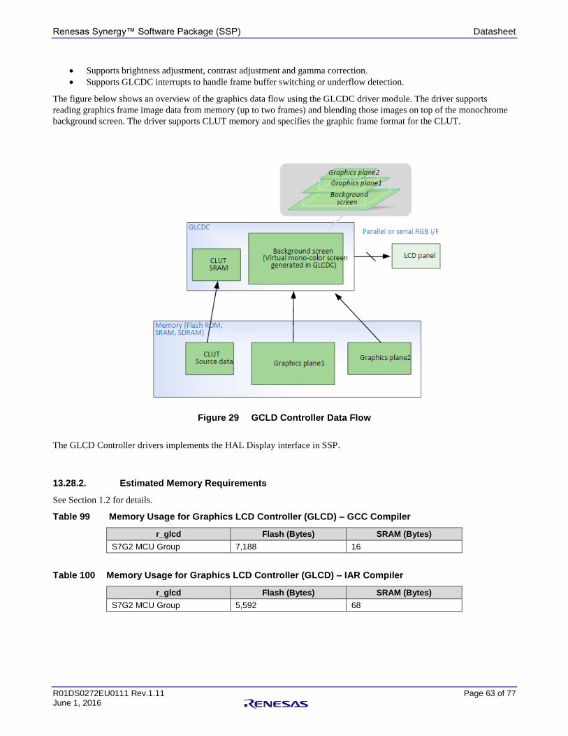
Renesas Synergy™ Software Package (SSP) Datasheet
R01DS0272EU0111 Rev.1.11 Page 63 of 77 June 1, 2016
Supports brightness adjustment, contrast adjustment and gamma correction.
Supports GLCDC interrupts to handle frame buffer switching or underflow detection.
The figure below shows an overview of the graphics data flow using the GLCDC driver module. The driver supports
reading graphics frame image data from memory (up to two frames) and blending those images on top of the monochrome
background screen. The driver supports CLUT memory and specifies the graphic frame format for the CLUT.
Figure 29 GCLD Controller Data Flow
The GLCD Controller drivers implements the HAL Display interface in SSP.
13.28.2. Estimated Memory Requirements
See Section 1.2 for details.
Table 99 Memory Usage for Graphics LCD Controller (GLCD) – GCC Compiler
r_glcd Flash (Bytes) SRAM (Bytes)
S7G2 MCU Group 7,188 16
Table 100 Memory Usage for Graphics LCD Controller (GLCD) – IAR Compiler
r_glcd Flash (Bytes) SRAM (Bytes)
S7G2 MCU Group 5,592 68

Renesas Synergy™ Software Package (SSP) Datasheet
R01DS0272EU0111 Rev.1.11 Page 64 of 77 June 1, 2016
13.29. Watchdog Timer (WDT)
13.29.1. Component Introduction
WDT driver in SSP supports the WDT peripheral on Synergy MCUs. This driver configures the Watchdog Timer (WDT)
Interface and when the WDT underflows or is refreshed outside of the permitted refresh window, one of the following
events will occur based on the configuration:
Resetting of the device
Generation of an NMI
WDT driver provides the ability to configure the operation of WDT (when used in register start mode), refresh the
watchdog, read the timer value and read and clear status flags.
The WDT and IWDT drivers implements the WDT HAL interface in SSP.
13.29.2. Estimated Memory Requirements
See Section 1.2 for details.
Table 101 Memory Usage for Watchdog Timer (WDT) – GCC Compiler
r_wdt Flash (Bytes) SRAM (Bytes)
S7G2 MCU Group 951 4
S3A7 MCU Group 951 4
S124 MCU Group 971 4
Table 102 Memory Usage for Watchdog Timer (WDT) – IAR Compiler
r_wdt Flash (Bytes) SRAM (Bytes)
S7G2 MCU Group 740 4
S3A7 MCU Group 740 4
S124 MCU Group 764 4
13.30. Independent Watchdog Timer (IWDT)
13.30.1. Component Introduction
The Independent Watchdog Timer (IWDT) peripheral in Synergy MCUs consists of a 14-bit down counter that must be
serviced periodically to prevent counter underflow. The IWDT driver supports the IWDT peripheral on Synergy MCUs.
This driver configures the Watchdog Timer (WDT) Interface and when the WDT underflows or is refreshed outside of the
permitted refresh window, one of the following events will occur based on the configuration:
Resetting of the device
Generation of an NMI
The IWDT driver provides ability to refresh the independent watchdog, read the timer value and read and clear status flags.
When used in NMI output mode the callback to be called by the NMI ISR can be registered.
The WDT and IWDT drivers implements the WDT HAL interface in SSP.
13.30.2. Estimated Memory Requirements
See Section 1.2 for details.
Renesas Synergy™ Software Package (SSP) Datasheet
R01DS0272EU0111 Rev.1.11 Page 65 of 77 June 1, 2016
Table 103 Memory Usage for Independent Watchdog Timer (IWDT) – GCC Compiler
r_iwdt Flash (Bytes) SRAM (Bytes)
S7G2 MCU Group 844 4
S3A7 MCU Group 844 4
S124 MCU Group 872 4
Table 104 Memory Usage for Independent Watchdog Timer (IWDT) – IAR Compiler
r_iwdt Flash (Bytes) SRAM (Bytes)
S7G2 MCU Group 648 4
S3A7 MCU Group 648 4
S124 MCU Group 668 4
13.31. Analog to Digital Converter (ADC)
13.31.1. Component Introduction
The HAL driver supports ADC12 and ADC14 peripherals available on the Synergy microcontroller hardware.
The ADC driver controls the ADC on a Synergy microcontroller according to the user configuration, it can access both
ADC units on the MCU and configure them for single scan, continuous scan, and group scan modes. When a scan is
complete and a callback is available (with interrupts enabled), the driver invokes the callback function.
If interrupts are not enabled, the driver checks the scan status to poll if the scan is complete and provides a function to read
the converted ADC result.
The ADC driver also supports reading the data from the on-chip temperature sensor and using it for comparison.
Group Mode Operation
The driver also supports group mode operation. In this mode, channels can be assigned to one of two groups: group-A or
group-B. A trigger is assigned for each group to start the scan. In group mode, only hardware triggers can be used, as
opposed to normal mode, where software triggers or an external trigger can be used.
The ADC Driver implements the ADC HAL interface in SSP.
13.31.2. Estimated Memory Requirements
See Section 1.2 for details.
Table 105 Memory Usage for Analog to Digital Converter (ADC) – GCC Compiler
r_adc Flash (Bytes) SRAM (Bytes)
S7G2 MCU Group 1,505 40
S3A7 MCU Group 1,181 40
S124 MCU Group 1,217 40
Table 106 Memory Usage for Analog to Digital Converter (ADC) – IAR Compiler
r_adc Flash (Bytes) SRAM (Bytes)
S7G2 MCU Group 1,264 40
S3A7 MCU Group 976 40
S124 MCU Group 1,080 40
Renesas Synergy™ Software Package (SSP) Datasheet
R01DS0272EU0111 Rev.1.11 Page 66 of 77 June 1, 2016
13.32. Factory Microcontroller Information (FMI)
13.32.1. Component Introduction
The FMI driver reads the FMIFRT (Factory MCU Information Flash Root Table) on a Synergy microcontroller for the
address of the start of the table in flash. It sets the caller’s pointer the Product Information record from the table.
The FMI Driver implements the FMI HAL interface in SSP.
13.32.2. Estimated Memory Requirements
See Section 1.2 for details.
Table 107 Memory Usage for Factory Microcontroller Information (FMI) – GCC Compiler
r_fmi Flash (Bytes) SRAM (Bytes)
S7G2 MCU Group 121 0
S3A7 MCU Group 121 0
Table 108 Memory Usage for Factory Microcontroller Information (FMI) – IAR Compiler
r_fmi Flash (Bytes) SRAM (Bytes)
S7G2 MCU Group 104 0
S3A7 MCU Group 104 0
13.33. Low Power Mode (LPM)
13.33.1. Component Introduction
The LPM driver provides access and configuration of the MCU operating power control modes using the Low Power Mode
hardware peripheral.
The LPM driver supports following operating power control modes:
Low-voltage mode
Low-speed mode
Middle-speed mode
High-speed mode
Subosc-speed mode
The LPM driver supports the following low power modes:
Deep Software Standby mode
Software Standby mode
Sleep mode
Snooze mode
The LPM driver supports reducing power consumption when in deep stand-by mode via internal power supply control and
resetting the states of IO ports. The LPM driver supports disabling and enabling of the MCUs other hardware peripherals.
Additional functionality supported: Enable/disable of hardware peripheral for additional power reduction.
The LPM Driver implements the LPM HAL interface in SSP.
13.33.2. Estimated Memory Requirements
See Section 1.2 for details.

Renesas Synergy™ Software Package (SSP) Datasheet
R01DS0272EU0111 Rev.1.11 Page 67 of 77 June 1, 2016
Table 109 Memory Usage for Low Power Mode – GCC Compiler
r_lpm Flash (Bytes) SRAM (Bytes)
S7G2 MCU Group 1,605 0
S3A7 MCU Group 1,109 0
S124 MCU Group 1,113 0
Table 110 Memory Usage for Low Power Mode – IAR Compiler
r_lpm Flash (Bytes) SRAM (Bytes)
S7G2 MCU Group 1,168 0
S3A7 MCU Group 836 0
S124 MCU Group 832 0
13.34. Controller Area Network (CAN)
13.34.1. Component Introduction
The CAN driver supports the CAN peripherals available on the Synergy microcontroller hardware. The API provides open,
close, read, write, control and information functions. The driver allows for bit timing configuration as defined in the CAN
specification and can be configured for up to 32 transmit or receive mailboxes with standard or extended ID frames.
Receive mailboxes can be configured to capture either Data or Remote CAN Frames. A user callback function can be
defined, causing the driver to invoke the callback when transmit, receive or error interrupts are received. The callback
provides the argument to indicate the channel, mailbox and the event.
The CAN Driver implements the CAN HAL interface in SSP.
13.34.2. Estimated Memory Requirements
See Section 1.2 for details.
Table 111 Memory Usage for Controller Area Network – GCC Compiler
r_can Flash (Bytes) SRAM (Bytes)
S7G2 MCU Group 1,509 56
S3A7 MCU Group 1,441 28
S124 MCU Group 1,477 28
Table 112 Memory Usage for Controller Area Network – IAR Compiler
r_can Flash (Bytes) SRAM (Bytes)
S7G2 MCU Group 1,568 56
S3A7 MCU Group 1,500 28
S124 MCU Group 1,552 28
Renesas Synergy™ Software Package (SSP) Datasheet
R01DS0272EU0111 Rev.1.11 Page 68 of 77 June 1, 2016
13.35. Serial Sound Interface (SSI)
13.35.1. Component Introduction
The SSI driver supports the SSI peripheral in I2S master mode on the Synergy microcontroller hardware. The driver
provides a generic API for serial audio communication using the I2S serial communication protocol. The driver is typically
used to send and receive uncompressed audio in master mode.
The I2S Driver used with the SSI peripheral in I2S master mode supports the following features in addition to the standard
I2S protocol:
Full-duplex I2S communication (SSI channel 0 only)
Interrupt driven data transmission and reception
Integration with the DTC transfer module
The SSI driver implements the I2S HAL interface in SSP.
13.35.2. Estimated Memory Requirements
See Section 1.2 for details.
Table 113 Memory Usage for Serial Sound Interface – GCC Compiler
r_ssi Flash (Bytes) SRAM (Bytes)
S7G2 MCU Group 4,053 8
S3A7 MCU Group 4,053 8
Table 114 Memory Usage for Serial Sound Interface – IAR Compiler
r_ssi Flash (Bytes) SRAM (Bytes)
S7G2 MCU Group 4,260 8
S3A7 MCU Group 4,260 8
13.36. Parallel Data Capture Unit (PDC)
13.36.1. Component Introduction
The PDC (Parallel Data Capture Unit) driver can be used for capturing image data from a camera module. The PDC driver
supports the PDC peripheral available on the Synergy microcontroller hardware.
PDC starts a capture from a connected and configured camera. When a capture is complete and a callback is available (with
interrupts enabled), the driver invokes the callback with the argument which provides a pointer to the buffer where the
captured image is stored. The event causing the callback is also provided.
The PDC driver implements the PDC interface in SSP.
13.36.2. Estimated Memory Requirements
See Section 1.2 for details.

Renesas Synergy™ Software Package (SSP) Datasheet
R01DS0272EU0111 Rev.1.11 Page 69 of 77 June 1, 2016
Table 115 Memory Usage for Parallel Data Capture – GCC Compiler
r_pdc Flash (Bytes) SRAM (Bytes)
S7G2 MCU Group 1,788 4
Table 116 Memory Usage for Parallel Data Capture – IAR Compiler
r_pdc Flash (Bytes) SRAM (Bytes)
S7G2 MCU Group 1,536 4
13.37. Low Voltage Detection (LVD)
13.37.1. Component Introduction
The LVD (Low Voltage Detection) driver provides access to the configuration of the Low Power Modes hardware
peripheral in Synergy Microcontrollers.
The LVD driver supports configuration of the LVD monitors of the Synergy MCUs. The LVD driver provides
configuration structures that provide all the information needed to fully configure a single LVD monitor. One instance of
the LVD driver is needed per instance of LVD monitor with the exception of the LVD0 monitor. The LVD0 monitor is not
configurable at runtime and must be configured at compile time via the OFS1 register.
The LVD1 and LVD2 monitors are both configurable at runtime and are configured by this driver. The open function allows
the user to configure and enable an LVD monitor with a single function call. The close function disables the LVD monitor.
The statusGet function returns the current status of the LVD monitor. The statusGet function should be used if the driver is
in polling mode, without the LVD monitor interrupt enabled. The monitor status consists of two flags, the first flag is a
latched flag called crossing_detected, which indicates whether or not the voltage being monitored has crossed the voltage
threshold. In polling mode, this flag must be cleared via a call to statusClear. The flag does not need to be cleared explicitly
if the LVD interrupt is in use, it will be cleared in the LVD interrupt by the driver code after the user callback function is
called. The other flag, current_state, is the instantaneous status of the monitored voltage with respect to the voltage
threshold. This flag is not latched and will change as the monitored voltage changes.
The LVD driver implements the Low Voltage Detection Interface in SSP.
13.37.2. Estimated Memory Requirements
See Section 1.2 for details.
Table 117 Memory Usage for Low Voltage Detection – GCC Compiler
r_lvd Flash (Bytes) SRAM (Bytes)
S7G2 MCU Group 1,590 40
S3A7 MCU Group 1,534 40
S124 MCU Group 1,542 40
Table 118 Memory Usage for Low Voltage Detection – IAR Compiler
r_lvd Flash (Bytes) SRAM (Bytes)
S7G2 MCU Group 1,320 40
S3A7 MCU Group 1,260 40
S124 MCU Group 1,260 40

Renesas Synergy™ Software Package (SSP) Datasheet
R01DS0272EU0111 Rev.1.11 Page 70 of 77 June 1, 2016
13.38. General PWM Timer with Input Capture (GPT_INPUT_CAPTURE)
13.38.1. Component Introduction
The GPT Input Capture driver supports the in General PWM Timer (GPT) with Input Capture in Synergy Microcontrollers.
The Input Capture Driver configures a timer to measure pulse widths. When a measurement is captured or the counter
overflows, a callback is called from a CPU interrupt with the measurement data.
The GPT Input Capture driver implements the Input Capture Driver Interface in SSP.
13.38.2. Estimated Memory Requirements
See Section 1.2 for details.
Table 119 Memory Usage for GPT Input Capture – GCC Compiler
r_gpt_input_capture Flash (Bytes) SRAM (Bytes)
S7G2 MCU Group 2,847 56
S3A7 MCU Group 2,447 56
S124 MCU Group 2,259 56
Table 120 Memory Usage for GPT Input Capture – IAR Compiler
r_gpt_input_capture Flash (Bytes) SRAM (Bytes)
S7G2 MCU Group 1,536 56
S3A7 MCU Group 1,512 56
S124 MCU Group 1,668 56
14. Board Support Package (BSP)
14.1. Component Introduction
The SSP includes BSPs for DK-S7G2, PE-HMI1, DK-S3A7, DK-S124 and SK-S7G2 kits. The BSP is responsible for
getting the MCU from reset to the user’s application (the main() function). Before reaching the user’s application, the
BSP sets up the stacks, heap, clocks, interrupts, and C runtime environment. The BSP also configures and sets up the port
I/O pins and performs any board specific initializations. The key features of the BSPs provided with SSP are:
Support for designated kits
Creation of custom BSPs using e2 studio
System initialization and configuration during startup
Software and hardware locking/unlocking
Register protection
CMSIS compliant
Standardized definitions for processor peripherals
Standardized access functions to access processor features
Standardized function names for system exception handlers
Standardized functions for system initialization.
Standardized software variables for clock speed information

Renesas Synergy™ Software Package (SSP) Datasheet
R01DS0272EU0111 Rev.1.11 Page 71 of 77 June 1, 2016
Figure 30 Board Support Package
14.1.1. Estimated Memory Requirements
See Section 1.2 for details.
Table 121 Memory Usage for Board Support Package – GCC Compiler
BSP Flash (Bytes) SRAM (Bytes)
DK-S7G2 11,269 754
DK-S3A7 10,789 745
DK-S124 7,893 143
Table 122 Memory Usage for Board Support Package – IAR Compiler
BSP Flash (Bytes) SRAM (Bytes)
DK-S7G2 10,380 793
DK-S3A7 9,982 785
DK-S124 7,118 173
15. SSP System Performance – Warranted and Non-Warranted
This section describes the SSP system performance measurements and the environment in which they were measured for
the SSP running on specified Synergy hardware, typically a Synergy Development Kit. There are two portions to some of
the stated benchmarking and performance test results sections:
Measured results that are warranted by Renesas under the SSP warranty policy.
Measured results that are NOT covered by the SSP warranty policy but are typical characterizations. These results
are useful indicators of performance to help you plan your system design.
Individual benchmarking and performance characterization depends on the version and configuration of the test
environment. For each individual test, the test environment is be specified.
Application Program
BSP
HAL
Application
Framework
X-WareTM
USBXTM Th
rea
dX
®NetXTM
FileX®
GUIXTM
Shared I/F
SSP
Synergy
MCU
Renesas Synergy™ Software Package (SSP) Datasheet
R01DS0272EU0111 Rev.1.11 Page 72 of 77 June 1, 2016
For SSP warranty claims, the claimant must identify which particular test (by particular section number within this
performance portion of the datasheet). The claimant must reproduce the suspected errant SSP behavior while operating
within the specified environment that is described for the particular test. If the errant SSP behavior is reproduced within the
specified environment, a SSP warranty claim can be made by contacting your local Renesas sales representative or affiliate
to process your claim. The claimant must hold a valid SSP Development/Production license to make a SSP warranty claim.
Once the claim has been processed by Renesas, the claimant will be notified of the resolution status of the warranty claim
within seven days of receipt.
NOTE: Renesas warranties these performance characteristics to within +/- 5% of reported scores or specifications.
The specified test environment, per individual test, will include but may be not limited to these elements:
SSP release version upon which the test software was built
Test software release version
Compiler version and optimization settings used to build the test software
Development environment tool version and configuration used to build the test software
Hardware kit type – typically a Synergy Development Kit with exact kit version number, on which the test
software was executed
o The kit, by default, also indicates the Synergy MCU type with CPU core type and clock speed
Other configurations that may vary from one test to another depending on the test
o Memory access such as
CPU instruction execution out of on-chip Flash memory or SRAM, external XIP Flash memory
or SDRAM, etc.
Source of data - USB-flash drive for file system, SD card, QSPI Flash memory, etc.
Individual benchmark and performance tests selected for SSP datasheet testing include those that represent real-world use
cases for embedded MCU applications as well as industry-standard benchmark tests. Some of the benchmark test software
used in SSP testing is widely available as open source, or it is easily licensed.
15.1. MCU-level Performance Metrics
15.1.1. Test Environments
Table 123 Test Environments for Performance Metrics
Test Environment Part Number and Revision/Version
DK-S7G2 Development Kit YSDKS7G2S30WS2 kit, v3.0 PCB, ARM® Cortex®-M4 CPU operating
frequency 240 MHz
Synergy Software Package SSP v.1.1.0
Test software https://www.eembc.org/coremark/register.php, EEMBC Version 1.0
e2 studio ISDE tool ISDE 5.0.0.043 with SSP 1.1.0+build.3
Compilers
GCC Compiler 4.9.3 20150529 (release)
GCC Compiler Optimization -O3, no debug
IAR C/C++ Compiler 7040005
IAR Compiler Optimization High speed, no size constraints

Renesas Synergy™ Software Package (SSP) Datasheet
R01DS0272EU0111 Rev.1.11 Page 73 of 77 June 1, 2016
Test Environment Part Number and Revision/Version
DK-S3A7 Development Kit YSDKS3A7E20, V2.0 PCB, ARM® Cortex®-M4 CPU operating
frequency 48 MHz
Synergy Software Package SSP v.1.1.0
Test software https://www.eembc.org/coremark/register.php, EEMBC Version 1.0
e2 studio ISDE tool ISDE 5.0.0.043 with SSP 1.1.0+build.3
Compilers
GCC Compiler 4.9.3 20150529 (release)
GCC Compiler Optimization -O3 no debug
IAR C/C++ Compiler 7040005
IAR Compiler Optimization High speed, no size constraints
Test Environment Part Number and Revision/Version
DK-S124 Development Kit YSDKS124S20, V2.0 PCB, ARM® Cortex®-M0+ CPU operating
frequency 32 MHz
Synergy Software Package SSP v.1.1.0
Test software https://www.eembc.org/coremark/register.php, EEMBC Version 1.0
e2 studio ISDE tool ISDE 5.0.0.043 with SSP 1.1.0+build.3
Compilers
GCC Compiler 4.9.3 20150529 (release)
GCC Compiler Optimization -O3 no debug
IAR C/C++ Compiler 7040005
IAR Compiler Optimization High speed, no size constraints
15.1.2. Metrics Covered by SSP Warranty
15.1.2.1 EEMBC CoreMark®
A general purpose, run-time test of CPU core and memory sub-system performance that reflects typical embedded MCU
application requirements. EEMBC CoreMark is targeted to replace Dhrystone MIPS and is widely used in the embedded
MCU industry.
Table 124 Warranted Test Results for MCU-level Performance – Larger is better
CPU Toolchain Clock Iterations Time(sec) Coremarks
DK-S7G2
GCC 240Mhz 10000 21.93 456
GCC 200Mhz 10000 26.32 380
GCC 160Mhz 10000 29.39 340
GCC 80Mhz 6000 34.59 173
IAR 240Mhz 10000 14.79 676
IAR 200Mhz 10000 17.75 563
IAR 160Mhz 10000 19.18 521
IAR 80Mhz 6000 22.61 265
DK-S3A7
GCC 48Mhz 10000 96.34 104
GCC 24Mhz 10000 187.31 53
IAR 48Mhz 10000 63.66 157
IAR 24Mhz 10000 124.18 81
DK-S124
GCC 32Mhz 10000 199.17 50
IAR 32Mhz 10000 125.99 79

Renesas Synergy™ Software Package (SSP) Datasheet
R01DS0272EU0111 Rev.1.11 Page 74 of 77 June 1, 2016
15.2. Operating System Performance Metrics
15.2.1. Metrics Covered by SSP Warranty
15.2.1.1 Thread-Metric Benchmarks
Express Logic’s Thread-Metric is a free-source benchmark suite for measuring RTOS performance, in particular the speed
with which an RTOS completes services for an application. This test is applicable to real-word embedded MCU system
applications using a Synergy family MCU with elements from Synergy Platform. Thread-Metric has a number of kernels
that are used for testing. The scores for each kernel is a composite value which indicate performance of the system with
higher score the indicating better performance. The Thread-Metric test suite consists of 8 distinct RTOS tests that are
designed to highlight commonly used aspects of an RTOS. The test measures the total number of RTOS events that can be
processed during a specific timer interval. A 30 second time interval is recommended and was used in our testing.
Basic Processing Test
This is the baseline test consisting of a single thread. This should execute the same on every operating system. Test values
from testing with different RTOS products should be scaled relative to the difference between the values of this test.
Cooperative Scheduling Test
This test consists of 5 threads created at the same priority that voluntarily releases control to each other in a round-robin
fashion. Each thread will increment its run counter and then relinquish to the next thread. At the end of the test the
counters will be verified to make sure they are valid (should all be within 1 of the same value). If valid, the numbers will be
summed and presented as the result of the cooperative scheduling test.
Preemptive Scheduling Performance: The Preemptive context switching test is much more complex, and reflects a real-
time computing system that has to deal with different thread priorities. It measures the time the RTOS takes to change the
execution context from one thread to a higher-priority thread, which preempts the executing thread. The steps are:
1. Five threads are created that each have a unique priority.
2. The threads run until preempted by a higher-priority thread.
3. All threads except the lowest-priority thread are in a suspended state.
4. The lowest-priority thread resumes the next highest-priority thread, and so on until the highest-priority thread
executes.
5. Each thread increments its run count and then suspends.
6. Once processing returns to the lowest-priority thread, it increments its run counter and again resumes the next
highest-priority thread, starting the process over again.
Interrupt Processing Test
This test consists of a single thread. The thread will cause an interrupt (typically implemented as a trap), which will result in
a call to the interrupt handler. The interrupt handler will increment a counter and then post to a semaphore. After the
interrupt handler completes, processing returns to the test thread that initiated the interrupt. The thread then retrieves the
semaphore set by the interrupt handler, increments a counter and then generates another interrupt.
Interrupt Preemption Processing Test
This test is similar to the previous interrupt test. The big difference is the interrupt handler in this test resumes a higher
priority thread, which causes thread preemption.
Message Processing: This test consists of a thread sending a 16 byte message to a queue and retrieving the same 16 byte
message from the queue. After the send/receive sequence is complete, the thread increments its run counter.
Synchronization Processing Test
This test consists of a thread getting a semaphore and then immediately releasing it. After the get/put cycle completes, the
thread will increment its run counter.
Memory Kernel Performance: The Thread-Metric memory kernel test is a memory allocation and deallocation test, and
measures the time it takes the RTOS to allocate a fixed-size block of memory for a thread. This test is designed to test
memory allocation of 128-byte blocks.

Renesas Synergy™ Software Package (SSP) Datasheet
R01DS0272EU0111 Rev.1.11 Page 75 of 77 June 1, 2016
Table 125 Warranted Results for Operating System Performance
Unit Iterations During a 30-second period. Higher value means better
performance.
Test Name Board GCC (O3) IAR (High Speed with no size
constraints)
Basic processing S7G2-DK v3.0
240 MHz
439244 530201
Cooperative scheduling 35188454 30714823
Interrupt preemption processing 12161341 12202467
Interrupt processing 41616178 44169254
Memory allocation 48976742 47056172
Message processing 27887378 29236915
Preemptive scheduling 15719523 15105745
Synchronization processing 53330363 58533011
Basic processing S3A7-DK v2.0
48 MHz
108103 137006
Cooperative scheduling 8777882 7404473
Interrupt preemption processing 2974450 2789951
Interrupt processing 10585896 10743714
Memory allocation 11997244 11800347
Message processing 6604077 7051399
Preemptive scheduling 3869934 3602105
Synchronization processing 13842933 13087628
Basic processing S124-DK v1.0
24 MHz 46832 61050
Cooperative scheduling 3492884 3197920
Interrupt preemption processing 1315446 1242607
Interrupt processing 4643123 4497960
Memory allocation 5493767 5140473
Message processing 2834284 2853931
Preemptive scheduling 1721221 1616711
Synchronization processing 6151139 5898746
15.3. Networking Performance Metrics
15.3.1. Metrics Covered by SSP Warranty
15.3.1.1 iPerf Benchmark
The industry standard iPerf benchmark suite, an open-source benchmark suite that runs on a Linux or Windows host was
used for network performance testing of the SSP’s NetX TCP/IP networking stack. Specific focus is on TCP performance
and measured network throughput as the key performance indicator. iPerf and instructions can be found here:
http://sourceforge.net/projects/iperf/asdf. For this test, iPerf 2.0.2.7 was used.

Renesas Synergy™ Software Package (SSP) Datasheet
R01DS0272EU0111 Rev.1.11 Page 76 of 77 June 1, 2016
Table 126 Warranted Results for Networking Performance – iPerf
Test Results:
Test Case GCC:
Compiler options: -O2
IAR:
High speed, no size constraints
TCP Transmit Test: Throughput (Mbps): 35 37
TCP Receive Test: Throughput (Mbps): 93 93
UDP Transmit Test: Throughput (Mbps): 93 93
UDP Receive Test: Throughput (Mbps): 81 80
15.4. File System Performance Metrics
15.4.1. Metrics Covered by SSP Warranty
15.4.1.1 PostMark Benchmark
PostMark is the benchmark used in the NetApp Technical Report TR-3022, "PostMark: A New File System Benchmark".
The paper fully explains how to use this tool. PostMark measures performance simulating performance in the small-file
regime used by Internet software, especially Electronic mail, Netnews, and web-based commerce doing File Create, Read,
Write, Append, Close. At its essence, PostMark is a benchmark designed to simulate the behavior of mail servers.
PostMark consists of three phases. In the first phase a pool of files are created. In the next phase four types of transactions
are executed: files are created, deleted, read, and appended to. In the last phase, all files in the pool are deleted. We selected
a configuration that specified a maximum of 200 files and 500 transactions. Each transaction consists of either a read or
append operation, and a create or delete operation, so the workload consisted of creating 200 files, executing a sequence of
transactions, and deleting the files that remained after the transaction sequence. The exact sequence of operations is
specified by a pseudo-random number generator.
The metric for this test is the number of seconds required to execute this workload. The split-out of the file Create, Read,
Append, and then Delete functions, PostMark was taken “out of the box” and combined into a single workload.
Table 127 Warranted Results for File System Performance
Test Results: DK-S7G2
Test Case GCC –O2 IAR –OH Speed
Time: 44.81 seconds 44.91 seconds
Renesas Synergy™ Software Package (SSP) Datasheet
R01DS0272EU0111 Rev.1.11 Page 77 of 77 June 1, 2016
Revision History Renesas SynergyTM Software Package (SSP) Datasheet
Rev. Date
Description
Page Summary
0.8 October
2015
All Initial release for SSP v1.0.0 beta.
0.81 October
2015
64-66 Copyright statement and Technical Document Disclaimer added.
All Minor editorial updates. Page print size corrected.
0.90 December
2015
All Module descriptions improved or added.
1.00 January
2016
All Editorial updates. Performance data added.
1.01 February
2016
All Changes for SSP release 1.1.0-alpha. All performance data changed to TBD.
New modules added.
1.10 May 2016 All Changes for SSP release 1.1.0.
1.11 June 2016 All Added performance data for SSP modules.

Notice
1. Descriptions of circuits, software and other related information in this document are provided only to illustrate the operation of semiconductor products and application examples. You are fully responsible for
the incorporation of these circuits, software, and information in the design of your equipment. Renesas Electronics assumes no responsibility for any losses incurred by you or third parties arising from the use
of these circuits, software, or information.
2. Renesas Electronics has used reasonable care in preparing the information included in this document, but Renesas Electronics does not warrant that such information is error free. Renesas Electronics
assumes no liability whatsoever for any damages incurred by you resulting from errors in or omissions from the information included herein.
3. Renesas Electronics does not assume any liability for infringement of patents, copyrights, or other intellectual property rights of third parties by or arising from the use of Renesas Electronics products or
technical information described in this document. No license, express, implied or otherwise, is granted hereby under any patents, copyrights or other intellectual property rights of Renesas Electronics or
others.
4. You should not alter, modify, copy, or otherwise misappropriate any Renesas Electronics product, whether in whole or in part. Renesas Electronics assumes no responsibility for any losses incurred by you or
third parties arising from such alteration, modification, copy or otherwise misappropriation of Renesas Electronics product.
5. Renesas Electronics products are classified according to the following two quality grades: "Standard" and "High Quality". The recommended applications for each Renesas Electronics product depends on
the product's quality grade, as indicated below.
"Standard": Computers; office equipment; communications equipment; test and measurement equipment; audio and visual equipment; home electronic appliances; machine tools; personal electronic
equipment; and industrial robots etc.
"High Quality": Transportation equipment (automobiles, trains, ships, etc.); traffic control systems; anti-disaster systems; anti-crime systems; and safety equipment etc.
Renesas Electronics products are neither intended nor authorized for use in products or systems that may pose a direct threat to human life or bodily injury (artificial life support devices or systems, surgical
implantations etc.), or may cause serious property damages (nuclear reactor control systems, military equipment etc.). You must check the quality grade of each Renesas Electronics product before using it
in a particular application. You may not use any Renesas Electronics product for any application for which it is not intended. Renesas Electronics shall not be in any way liable for any damages or losses
incurred by you or third parties arising from the use of any Renesas Electronics product for which the product is not intended by Renesas Electronics.
6. You should use the Renesas Electronics products described in this document within the range specified by Renesas Electronics, especially with respect to the maximum rating, operating supply voltage
range, movement power voltage range, heat radiation characteristics, installation and other product characteristics. Renesas Electronics shall have no liability for malfunctions or damages arising out of the
use of Renesas Electronics products beyond such specified ranges.
7. Although Renesas Electronics endeavors to improve the quality and reliability of its products, semiconductor products have specific characteristics such as the occurrence of failure at a certain rate and
malfunctions under certain use conditions. Further, Renesas Electronics products are not subject to radiation resistance design. Please be sure to implement safety measures to guard them against the
possibility of physical injury, and injury or damage caused by fire in the event of the failure of a Renesas Electronics product, such as safety design for hardware and software including but not limited to
redundancy, fire control and malfunction prevention, appropriate treatment for aging degradation or any other appropriate measures. Because the evaluation of microcomputer software alone is very difficult,
please evaluate the safety of the final products or systems manufactured by you.
8. Please contact a Renesas Electronics sales office for details as to environmental matters such as the environmental compatibility of each Renesas Electronics product. Please use Renesas Electronics
products in compliance with all applicable laws and regulations that regulate the inclusion or use of controlled substances, including without limitation, the EU RoHS Directive. Renesas Electronics assumes
no liability for damages or losses occurring as a result of your noncompliance with applicable laws and regulations.
9. Renesas Electronics products and technology may not be used for or incorporated into any products or systems whose manufacture, use, or sale is prohibited under any applicable domestic or foreign laws or
regulations. You should not use Renesas Electronics products or technology described in this document for any purpose relating to military applications or use by the military, including but not limited to the
development of weapons of mass destruction. When exporting the Renesas Electronics products or technology described in this document, you should comply with the applicable export control laws and
regulations and follow the procedures required by such laws and regulations.
10. It is the responsibility of the buyer or distributor of Renesas Electronics products, who distributes, disposes of, or otherwise places the product with a third party, to notify such third party in advance of the
contents and conditions set forth in this document, Renesas Electronics assumes no responsibility for any losses incurred by you or third parties as a result of unauthorized use of Renesas Electronics
products.
11. This document may not be reproduced or duplicated in any form, in whole or in part, without prior written consent of Renesas Electronics.
12. Please contact a Renesas Electronics sales office if you have any questions regarding the information contained in this document or Renesas Electronics products, or if you have any other inquiries.
(Note 1) "Renesas Electronics" as used in this document means Renesas Electronics Corporation and also includes its majority-owned subsidiaries.
(Note 2) "Renesas Electronics product(s)" means any product developed or manufactured by or for Renesas Electronics.
http://www.renesas.com
Refer to "http://www.renesas.com/" for the latest and detailed information.
Renesas Electronics America Inc.2801 Scott Boulevard Santa Clara, CA 95050-2549, U.S.A.Tel: +1-408-588-6000, Fax: +1-408-588-6130
Renesas Electronics Canada Limited9251 Yonge Street, Suite 8309 Richmond Hill, Ontario Canada L4C 9T3Tel: +1-905-237-2004
Renesas Electronics Europe LimitedDukes Meadow, Millboard Road, Bourne End, Buckinghamshire, SL8 5FH, U.KTel: +44-1628-585-100, Fax: +44-1628-585-900
Renesas Electronics Europe GmbH
Arcadiastrasse 10, 40472 Düsseldorf, GermanyTel: +49-211-6503-0, Fax: +49-211-6503-1327
Renesas Electronics (China) Co., Ltd.Room 1709, Quantum Plaza, No.27 ZhiChunLu Haidian District, Beijing 100191, P.R.ChinaTel: +86-10-8235-1155, Fax: +86-10-8235-7679
Renesas Electronics (Shanghai) Co., Ltd.Unit 301, Tower A, Central Towers, 555 Langao Road, Putuo District, Shanghai, P. R. China 200333Tel: +86-21-2226-0888, Fax: +86-21-2226-0999
Renesas Electronics Hong Kong LimitedUnit 1601-1611, 16/F., Tower 2, Grand Century Place, 193 Prince Edward Road West, Mongkok, Kowloon, Hong KongTel: +852-2265-6688, Fax: +852 2886-9022
Renesas Electronics Taiwan Co., Ltd.13F, No. 363, Fu Shing North Road, Taipei 10543, TaiwanTel: +886-2-8175-9600, Fax: +886 2-8175-9670
Renesas Electronics Singapore Pte. Ltd.80 Bendemeer Road, Unit #06-02 Hyflux Innovation Centre, Singapore 339949Tel: +65-6213-0200, Fax: +65-6213-0300
Renesas Electronics Malaysia Sdn.Bhd.Unit 1207, Block B, Menara Amcorp, Amcorp Trade Centre, No. 18, Jln Persiaran Barat, 46050 Petaling Jaya, Selangor Darul Ehsan, MalaysiaTel: +60-3-7955-9390, Fax: +60-3-7955-9510
Renesas Electronics India Pvt. Ltd.No.777C, 100 Feet Road, HALII Stage, Indiranagar, Bangalore, IndiaTel: +91-80-67208700, Fax: +91-80-67208777
Renesas Electronics Korea Co., Ltd.12F., 234 Teheran-ro, Gangnam-Gu, Seoul, 135-080, KoreaTel: +82-2-558-3737, Fax: +82-2-558-5141
SALES OFFICES
© 2016 Renesas Electronics Corporation. All rights reserved.
Colophon 5.0