Reliability Failure of Electronic Materials Devices
715
-
Upload
ashutoshsachan -
Category
Documents
-
view
1.034 -
download
185
description
reliability failure of electronic material
Transcript of Reliability Failure of Electronic Materials Devices
Reliability and Failure of Electronic
Materials and Devices

This Page Intentionally Left Blank
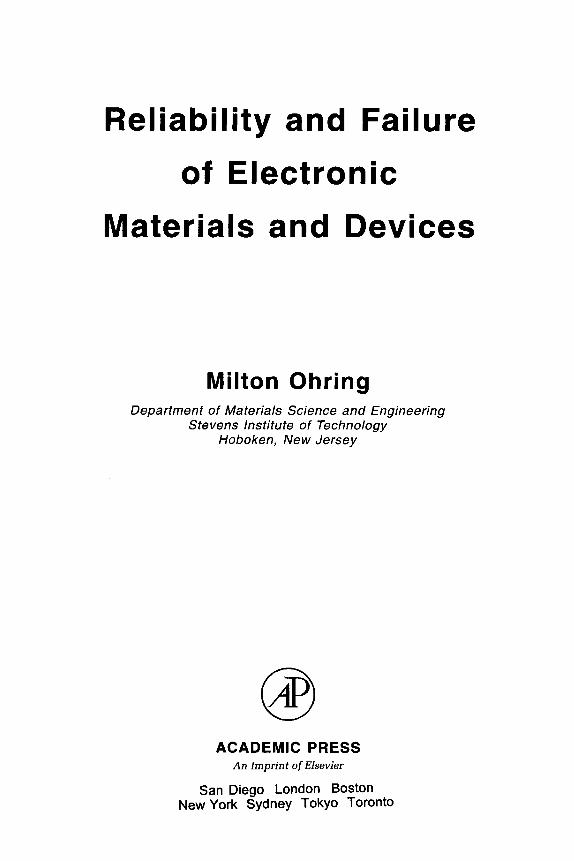
Reliability and Failure
of Electronic
Materials and Devices
Milton Ohring Department of Materials Science and Engineering
Stevens Institute of Tectinology Hoboken, New Jersey
ACADEMIC PRESS An Imprint of Elsevier
San Diego London Boston New York Sydney Tokyo Toronto
This book is printed on acid-free paper. ( ^
Copyright © 1998 by Academic Press.
All rights reserved. No part of this publication may be reproduced or transmitted in any form or by any means, electronic or mechanical, including photocopy, recording, or any information storage and retrieval system, without permission in writing from the publisher.
Permissions may be sought directly from Elsevier's Science and Technology Rights Department in Oxford, UK. Phone: (44) 1865 843830, Fax: (44) 1865 853333, e-mail: [email protected]. You may also complete your request on-line via the Elsevier homepage: http://www.elsevier.com by selecting "CXistomer Support" and then "Obtaining Permissions".
The cover image is an artist's rendition of an electrostatic spark discharge event that lasts less than one billionth of a second. This miniature lightning bolt from a charged object can easily damage a semiconductor device. The photo is courtesy of Wayne Tan, Advanced Micro Devices.
ACADEMIC PRESS An Imprint of Elsevier 525 B Street, Suite 1900, San Diego, CA 92101-4495, USA 1300 Boylston Street, Chestnut Hill, MA 02167, USA http://www.apnet.com
United Kingdom Edition published by ACADEMIC PRESS LIMITED An Imprint of Elsevier
24-28 Oval Road, Londcm NWl 7DX http://www.hbuk.co.uk/ap
Library of Congress Cataloging-in-Publication Data
Ohring, Milton, 1936-Reliability and failure of electronic materials and devices / Milton Ohring.
p. cm. Includes bibUographical references. ISBN-13: 978-0-12-524985-0 ISBN-10: 0-12-524985-3 1. Electronic apparatus and appHances—Reliability. 2. System failures (Engineering) I. Tide.
TK7870.23.037 1998 621.381—dc21 98-16084
CIP
ISBN-13: 978-0-12-524985-0 ISBN-10: 0-12-524985-3 Printed in the United States of America
06 MV 9 8 7 6 5 4 3

He whose works exceed his wisdom, his wisdom will endure. Ethics of the Fathers
In honor of my father, Max, ... a very reUable dad.

This Page Intentionally Left Blank
Contents
Acknowledgments xvii
Preface xix
Chapter 1 An Overview of Electronic Devices and Their Reliability 1 1.1 Electronic Products 1
1.1.1 Historical Perspective 1 1.1.2 Solid-state Devices 4 1.1.3 Integrated Circuits 4 1.1.4 Yield of Electronic Products. . 9
1.2 Reliability, Other " . . . ilities," and Definitions 13 1.2.1 Reliability 13 1.2.2 A Brief History of Reliability 14 1.2.3 MIL-HDBK-217 15 1.2.4 Long-Term Nonoperating Reliability 16 1.2.5 Availability, Maintainability, and Survivability 17
1.3 Failure Physics 17 1.3.1 Failure Modes and Mechanisms;
Reliable and Failed States 17 1.3.2 Conditions for Change 18 1.3.3 Atom Movements and Driving Forces 20 1.3.4 Failure Times and the Acceleration Factor 24 1.3.5 Load-Strength Interference 25 1.3.6 Semiconductor Device Degradation and Failure 27 1.3.7 Failure Frequency 28 1.3.8 The Bathtub Curve and Failure 29
1.4 Summary and Perspective 31 Exercises 32 References 35
VII
viii Contents
Chapter 2
Electronic Devices: How They Operate and Are Fabricated . . . 37 2.1 Introduction 37 2.2 Electronic Materials 38
2.2.1 Introduction 38 2.2.2 Semiconductors 39 2.2.3 Conductors 49 2.2.4 Insulators 52
2.3 Diodes 53 2.3.1 The p-n Junction 53 2.3.2 Contacts 55 2.3.3 Deviations from Ideal Junction Behavior 57
2.4 Bipolar Transistors 59 2.4.1 Transistors in General 59 2.4.2 Bipolar Junction Transistors 59
2.5 Field Effect Transistors 62 2.5.1 Introduction 62 2.5.2 The MOS Capacitor 63 2.5.3 MOS Field Effect Transistor 66 2.5.4 CMOS Devices 69 2.5.5 MOSFET Instabilities and Malfunction 70 2.5.6 Bipolar versus CMOS 71 2.5.7 Junction Field Effect Transistor (JFET) 72
2.6 Memories 74 2.6.1 Types of Memories 74 2.6.2 Memories Are Made of This! 76 2.6.3 Reliability Problems in Memories 77
2.7 GaAs Devices 79 2.7.1 Why Compound Semiconductor Devices? 79 2.7.2 Microwave Applications 80 2.7.3 The GaAs MESFET 81 2.7.4 High Electron Mobility Transistor (HEMT) 82 2.7.5 GaAs Integrated Circuits .82
2.8 Electro-optical Devices 84 2.8.1 Introduction 84 2.8.2 Solar Cells 84 2.8.3 PIN and Avalanche Photodiodes 85 2.8.4 Light Emitting Diodes (LEDs) 86 2.8.5 Semiconductor Lasers 87
2.9 Processing—The Chip Level 91 2.9.1 Introduction 91 2.9.2 Silicon Crystal Growth (1) 92
Contents ix
2.9.3 Epitaxy (2) 93 2.9.4 Ion Implantation (3) 94 2.9.5 Gate Oxide (4) 95 2.9.6 Polysilicon (5) 95 2.9.7 Deposited and Etched Dielectric Films (6,7,12) 95 2.9.8 Metallization (8-11) 96 2.9.9 Plasma Etching 99
2.9.10 Lithography 99 Exercises 100 References 102
Chapter 3 Defects, Contaminants and Yield 105 3.1 Scope 105 3.2 Defects in Crystalline Solids and Semiconductors 107
3.2.1 General Considerations 107 3.2.2 Point Defects 108 3.2.3 Dislocations 115 3.2.4 Grain Boundaries 122 3.2.5 Dislocation Defects in DRAMs—A Case Study 123
3.3 Processing Defects 125 3.3.1 Scope 125 3.3.2 Stress and Defects 127 3.3.3 Step Coverage 137
3.4 Contamination 141 3.4.1 Introduction 141 3.4.2 Process-Induced Contamination 142 3.4.3 Introduction to Particle Science 147 3.4.4 Combating Contamination 152
3.5 Yield 155 3.5.1 Definitions and Scope 155 3.5.2 Statistical Basis for Yield 157 3.5.3 Yield Modeling 159 3.5.4 Comparison with Experience 160 3.5.5 Yield and Reliability—What Is the Link? 162 3.5.6 Conclusion 168 Exercises 168 References 171
Chapter 4 The Mathematics of Failure and Reliability .175 4.1 Introduction 175
X Contents
4.2 Statistics and Definitions 177 4.2.1 Normal Distribution Function 177 4.2.2 "Six Sigma" 180 4.2.3 Accuracy and Precision 182 4.2.4 Failure Rates 182
4.3 All About Exponential, Lognormal and Weibull Distributions 184 4.3.1 Exponential Distribution Function 184 4.3.2 Lognormal Distribution 189 4.3.3 Weibull Distribution 193 4.3.4 Lognormal versus Weibull 196 4.3.5 Plotting Probability Functions as Straight Lines 196 4.3.6 Freak Behavior 199
4.4 System ReUability 202 4.4.1 Introduction 202 4.4.2 Redundancy in a Two-Laser System 205 4.4.3 How MIL-HDBK-217 Treats System Reliability 206
4.5 On the Physical Significance of Failure Distribution Functions 208
4.5.1 Introduction 208 4.5.2 The Weakest Link 208 4.5.3 The Weibull Distribution: Is There a Weak Link
to the Avrami Equation? 209 4.5.4 Physics of the Lognormal Distribution 211 4.5.5 Acceleration Factor 212 4.5.6 The Arrhenius Model 214 4.5.7 The Eyring Model 215 4.5.8 Is Arrhenius Erroneous? 218 4.5.9 The Bathtub Curve Revisited 219
4.6 Prediction Confidence and Assessing Risk 222 4.6.1 Introduction 222 4.6.2 Confidence Limits 222 4.6.3 Risky Reliability Modeling 224 4.6.4 Freak Failures 227 4.6.5 Minimizing Freak Failures 228
4.7 A Skeptical and Irreverent Summary 229 Exercises 231 References 235
Chapter 5 Mass Transport-Induced Failure 237 5.1 Introduction 237
Contents xi
5.2 Diffusion and Atom Movements in Solids 238 5.2.1 Mathematics of Diffusion 238 5.2.2 Diffusion Coefficients and Microstructure 240
5.3 Binary Diffusion and Compound Formation 242 5.3.1 Interdiffusion and the Phase Diagram 242 5.3.2 Compound Formation 244 5.3.3 The Kirkendall Effect 245 5.3.4 The Purple Plague 246
5.4 Reactions at Metal-Semiconductor Contacts 248 5.4.1 Introduction to Contacts 248 5.4.2 Al-Si Contacts 248 5.4.3 Metal Silicide Contacts to Silicon 252 5.4.4 Contacts to GaAs Devices 253
5.5 Electromigration Physics and Damage Models 259 5.5.1 Introduction 259 5.5.2 Physical Description of Electromigration 262 5.5.3 Temperature Distribution in Powered Conductors 264 5.5.4 Role of Stress 266 5.5.5 Structural Models for Electromigration Damage 267
5.6 Electromigration in Practice 273 5.6.1 Manifestations of Electromigration Damage 273 5.6.2 Electromigration in Interconnects: Current
and Temperature Dependence 276 5.6.3 Effect of Conductor Geometry and Grain Structure
on Electromigration 279 5.6.4 Electromigration Lifetime Distributions 281 5.6.5 Electromigration Testing 281 5.6.6 Combating Electromigration 283
5.7 Stress Voiding 284 5.7.1 Introduction 284 5.7.2 Origin of Stress in Metallizations 285 5.7.3 Vacancies, Stresses, Voids, and Failure 288 5.7.4 Role of Creep in Stress Voiding Failure 291 5.7.5 Stress Voiding at Vias 292
5.8 Failure of Incandescent Lamps 293 Exercises 296 References 300
Chapter 6 Electronic Charge-Induced Damage 303 6.1 Introduction 303
xii Contents
6.2 Aspects of Conduction in Insulators 304 6.2.1 Current-Voltage Relationships 304 6.2.2 Leakage Current 307 6.2.3 Si02—^Electrons, Holes, Ions, and Traps 308
6.3 Dielectric Breakdown 310 6.3.1 Introduction 310 6.3.2 A Brief History of Dielectric Breakdown Theories 311 6.3.3 Current Dielectric Breakdown Theories 312 6.3.4 Dielectric-Breakdown Testing: Ramp Voltage 316 6.3.5 Dielectric-Breakdown Testing: Constant Voltage 320 6.3.6 Ramp-Voltage and Constant-Voltage Tests:
Is There a Connection? 321 6.3.7 Electric-Field and Temperature-Acceleration
Factors 324 6.3.8 Plasma Charging Damage to Gate Oxides 325 6.3.9 Analogy between Dielectric and Mechanical
Breakdown of Solids 326 6.3.10 Discharges and Water Trees 328
6.4 Hot-Carrier Effects 330 6.4.1 Introduction 330 6.4.2 Hot Carriers 330 6.4.3 Hot Carrier Characteristics in MOSFET Devices 331 6.4.4 Models for Hot-Carrier Degradation 331 6.4.5 Hot-Carrier Damage in Other Devices 338 6.4.6 Combating Hot-Carrier Damage 338
6.5 Electrical Overstress and Electrostatic Discharge 339 6.5.1 Introduction 339 6.5.2 ESD Models 341 6.5.3 Thermal Analysis of ESD Failures 344 6.5.4 ESD Failure Mechanisms 347 6.5.5 Latent Failures 349 6.5.6 Guarding Against ESD 351 6.5.7 Some Common Myths About ESD 351 Exercises 352 References 355
Chapter 7 Environmental Damage to Electronic Products 359 7.1 Introduction 359 7.2 Atmospheric Contamination and Moisture 360
7.2.1 Sources of Airborne Contamination 360 7.2.2 Moisture Damage 363
Contents xiii
7.3 Corrosion of Metals 366 7.3.1 Introduction 366 7.3.2 Pourbaix Diagrams 367 7.3.3 Corrosion Rates 370 7.3.4 Damage Manifestations 370
7.4 Corrosion in Electronics 373 7.4.1 Overview 373 7.4.2 Accelerated Corrosion Testing 375 7.4.3 Corrosion of Specific Metals 376 7.4.4 Modeling Corrosion Damage 382
7.5 Metal Migration 385 7.5.1 Introduction 385 7.5.2 Metal Migration on Porous Substrates 386 7.5.3 Metal Migration on Ceramic Substrates 388 7.5.4 Mobile Ion Contamination in CMOS Circuits 390
7.6 Radiation Damage to Electronic Materials and Devices 391 7.6.1 A Historical Footnote 391 7.6.2 Some Definitions 391 7.6.3 Radiation Environments 392 7.6.4 Interaction of Radiation with Matter 393 7.6.5 Device Degradation Due to Ionizing Radiation 395 7.6.6 Soft Errors 398 7.6.7 Radiation Hardening of Devices 404 Exercises 405 References 408
Chapter 8 Packaging Materials, Processes, and Stresses 411 8.1 Introduction 411 8.2 IC Chip-Packaging Processes and Effects 415
8.2.1 Scope 415 8.2.2 First-Level Electrical Interconnection 418 8.2.3 Chip Encapsulation 428
8.3 Solders and Their Reactions 435 8.3.1 Introduction 435 8.3.2 Solder Properties 438 8.3.3 Metal-Solder Reactions 438
8.4 Second-Level Packaging Technologies 447 8.4.1 Introduction 447 8.4.2 Through Hole and Surface Mounting 447 8.4.3 Ball Grid Arrays 449 8.4.4 Reflow and Wave Soldering Processes 449 8.4.5 Defects in Solder Joints 451
xiv Contents
8.5 Thermal Stresses in Package Structures 452 8.5.1 Introduction 452 8.5.2 Chips Bonded to Substrates 454 8.5.3 Thermal Stress in Other Structures 460 Exercises 467 References 471
Chapter 9 Degradation of Contacts and Package
Interconnections 475 9.1 Introduction 475 9.2 The Nature of Contacts 476
9.2.1 Scope 476 9.2.2 Constriction Resistance 477 9.2.3 Heating Effects 479 9.2.4 Mass Transport Effects at Contacts 479 9.2.5 Contact Force 481
9.3 Degradation of Contacts and Connectors 482 9.3.1 Introduction 482 9.3.2 Mechanics of Spring Contacts 482 9.3.3 Normal Force Reduction in Contact Springs 486 9.3.4 Tribology 488 9.3.5 Fretting Wear Phenomena 489 9.3.6 Modeling Fretting Corrosion Damage 491
9.4 Creep and Fatigue of Solder 492 9.4.1 Introduction 492 9.4.2 Creep—An Overview 493 9.4.3 Constitutive Equations of Creep 494 9.4.4 Solder Creep 495 9.4.5 Fatigue—An Overview 498 9.4.6 Isothermal Fatigue of Solder 504
9.5 Reliability and Failure of Solder Joints 507 9.5.1 Introduction to Thermal Cycling Effects 507 9.5.2 Thermal-Stress Cycling of Surface-Mount
Solder Joints 512 9.5.3 Acceleration Factor for Solder Fatigue 516 9.5.4 Fracture of Solder Joints 517
9.6 Dynamic Loading Effects in Electronic Equipment 526 9.6.1 Introduction 526 9.6.2 Vibration of Electronic Equipment 527 Exercises 531 References 535

Contents xv
Chapter 10 Degradation and Failure of Electro-optical
Materials and Devices 539 10.1 Introduction 539 10.2 Failure and Reliability of Lasers and Light-Emitting Diodes 540
10.2.1 A Bit of History 540 10.2.2 Reliability Testing of Lasers and LEDs 541 10.2.3 Microscopic Mechanisms of Laser Damage 547 10.2.4 Electrostatic Discharge Damage to Lasers 554 10.2.5 Contact and Bonding ReHability 556
10.3 Thermal Degradation of Lasers and Optical Components 559 10.3.1 Introduction 559 10.3.2 Thermal Analysis of Heating 560 10.3.3 Laser-Induced Damage to Optical Coatings 561 10.3.4 Thermal Damage to Lasers 562
10.4 ReHability of Optical Fibers .568 10.4.1 Introduction 568 10.4.2 Optical Fiber Strength 571 10.4.3 Static Fatigue—Crack Growth and Fracture 574 10.4.4 Environmental Degradation of Optical Fiber 578
Exercises 582 References 585
Chapter 11
Characterization and Failure Analysis of Materials and Devices 587
11.1 Overview of Testing and Failure Analysis 587 11.1.1 Scope 587 11.1.2 Characterization Tools and Methods 591
11.2 Nondestructive Examination and Decapsulation 592 11.2.1 Radiography 592 11.2.2 Scanning Acoustic Microscopy 594 11.2.3 Analysis of FIND Particles 598 11.2.4 Decapsulation 599
11.3 Structural Characterization 603 11.3.1 Optical Microscopy 603 11.3.2 Electron Microscopy 604 11.3.3 Transmission Electron Microscopy 611 11.3.4 Focused Ion Beams 612
xvi Contents
11.4 Chemical Characterization 615 11.4.1 Introduction 615 11.4.2 Making Use of Core-Electron Transitions 615 11.4.3 Chemical Analysis by Means of Ions 619
11.5 Examining Devices Under Electrical Stress 621 11.5.1 Introduction 621 11.5.2 Emission Microscopy 621 11.5.3 Voltage Contrast Techniques 625 11.5.4 Thermography 630 11.5.5 Trends in Failure Analysis 635
Exercises 635 References 638
Chapter 12 Future Directions and Reliability Issues 641 12.1 Introduction 641 12.2 Integrated Circuit Technology Trends 642
12.2.1 Introduction 642 12.2.2 IC Chip Trends 642 12.2.3 Contamination Trends 648 12.2.4 Lithography 650 12.2.5 Packaging 651
12.3 Scaling 654 12.3.1 Introduction 654 12.3.2 Implications of Device ScaUng 656
12.4 Fundamental Limits 658 12.4.1 Introduction 658 12.4.2 Physical Limits 659 12.4.3 Material Limits 660 12.4.4 Device Limits 660
12.5 Improving Reliabihty 662 12.5.1 Reliabihty Growth 663 12.5.2 Failure Prediction: Stressor-Susceptibility
Interactions 664 12.5.3 Building In Reliabihty 665
Exercises 669 References 671
Appendix 673 Index 675
Acknowledgments
The idea for this book germinated in the classroom of Bell Laboratories, both at AT&T and Lucent Technologies, where I taught and organized several courses on reliability and failure of electronics over the past decade. Distilling the essence of the vast scattered information on this subject, first for course purposes and then into the text and figures that have emerged between these covers, would not have been possible without the resources of Bell Labs and the generous assistance of some very special people. Of these, two of my dear friends, Lucian (Lou) Kasprzak and Frank Nash, must be acknowledged first. Lou, an early observer of transistor hot-electron effects at IBM, is a member of the board of directors of the IEEE International Reliability Physics Symposia, while Frank, an expert in laser reliability at Bell Labs, wrote the incisive book. Estimating Device Reliability: Assessment of Credibility, Kluwer, (1993). Both stimulated my thinking on the direction of the book and helped me to acquire the research literature that was indispensable to its writing. Importantly, they dispelled some of my naivete about reliability, and helped me to fashion a cred-ible philosophy of the subject, something acquired only after lengthy grappling with the issues.
Students enrolled in courses for which books are simultaneously being writ-ten often leave their imprint on them. This is true of several of the students in the Stevens Institute-Bell Laboratories on-premises graduate program. There-fore, I want to thank both Gary Steiner and Jeff Murdock for critiquing various versions of the text. Gary additionally reviewed the exercises and enhanced the quality of several figures; Jeff assured me that the text was "Murdock-proof."
xvii
xviii Acknowledgments
Other students who tangibly contributed to the book are Ken Jola, Jim Bitetto, Ron Ernst, and Jim Reinhart.
Ephraim Suhir, Walter Brown, Matt Marcus, Alan English, King Tai, Sho Nakahara, George Chu, Reggie Farrow, Clyde Bethea and Dave Barr, all of Bell Laboratories, and Bob Rosenberg of IBM deserve thanks for their encourage-ment, helpful discussions, and publications. Despite their efforts I am solely responsible for any residual errors and holes in my understanding of the subject.
I am also grateful to the ever-helpful Nick Ciampa of Bell Laboratories for his technical assistance during the preparation of this book and generosity over the years. For help at important times I wish to acknowledge Pat Downes and Krisda Siangchaew. Lastly, thanks are owed to Zvi Ruder for supporting this project at Academic Press, and to Linda Hamilton and Julie Champagne for successfully guiding it through the process of publication.
My dear wife, Ahrona, has once again survived the birth of a book in the fam-ily, this time during a joyous period when our three grandchildren, Jake, Max, and Geffen, were bom. She and they were unfailing sources of inspiration.
M. Ohring
Preface
Reliability is an important attribute of all engineering endeavors that conjures up notions of dependability, trustworthiness, and confidence. It spells out a pre-scription for competitiveness in manufacturing because the lack of reliability means service failures that often result in inconvenience, personal injury, and financial loss. More pointedly, our survival in a high-tech future increasingly hinges on products based on microelectronics and optoelectronics where relia-bility and related manufacturing concerns of defects, quality, and yield are of critical interest. Despite their unquestioned importance these subjects are largely ignored in engineering curricula. Industry compensates for this educational neglect through on-the-job training. In the process, scientists and engineers of all backgrounds are recast into reliability "specialists" with many different attitudes toward reliability problems, and varied skills in solving them. The reliability practitioner must additionally be a detective, a statistician, and a judge capable of distinguishing between often conflicting data and strongly held opinions. This book attempts to systematically weave together those strands that compose the fabric of the training and practice of reliability engineers.
The multifaceted issues surrounding the reliability and failure of electronic materials and devices lie at the confluence of a large number of disciplinary streams that include materials science, physics, electrical engineering, chemistry, and mechanical engineering, as well as probability and statistics. I have tried to integrate the derivative subject matter of these disciplines in a coherent order and in the right proportions to usefully serve the following audiences:
• advanced undergraduate and first year graduate engineering and science stu-dents who are being introduced to the field,
xix
XX Preface
• reliability professionals and technicians who may find it a useful reference and guide to the literature on the subject, and
• technical personnel undergoing a career change.
While the emphasis of the book is on silicon microelectronics technology, reli-ability issues in compound semiconductor and electro-optical devices, optical fibers, and associated components are also addressed. The book starts with an introductory chapter that briefly defines the subject of semiconductor reliability, its concerns and historical evolution. Chapter 2 introduces electronic materials and devices, the way they are processed, how they are expected to behave, and the way they sometimes malfunction. The important subjects of intrinsic and manu-facturing defects, contamination, and product yield are the focus of Chapter 3.
Without Chapter 4 on the mathematics of reliability it is doubtful that the book title could include the word reliability. Historically, reliability has been inextrica-bly intertwined with statistics and probability theory. Even today a large segment of the reliability literature bears a strong hereditary relationship to these mathe-matical and philosophical antecedents. Nevertheless, "Hie failure of devices occurs due to natural laws of change, not to the finger of fate landing at random on one of group of devices and commanding/a/f (R.G. Stewart, IEEE Transac-tions on Reliability, R-15, No. 3, 95 (1966)). In a less charitable vein, R.A. Evans has pointed out that probability and statistical inference help us "quantify our ignorance" of failure mechanisms. Uncovering truth should be the objective instead. That is why the primary focus of the book and most of its contents deal with the physics of failure as refracted through the lenses of physical and materi-als science. With this understanding our treatment of reliability mathematics is largely limited to the elementary statistical handling of failure data and the simple implications that flow from such analyses. Nevertheless, reliability mathematics permeates the book since failure data are normally presented in these terms.
The midsection of the book spanning Chapters 5 through 10 is devoted to a treatment of the specific ways materials and devices degrade and fail both on the chip and packaging levels. Failure mechanisms discussed and modeled include those due to mass and electron transport, environmental and corrosion degrada-tion, mechanical stress, and optical as well as nuclear radiation damage. Most failures occurring within interconnections, dielectrics and insulation, contacts, semiconductor junctions, solders, and packaging materials can be sorted into one of these categories. Grouping according to operative failure mechanism, rather than specific device, material, or circuit element, underscores the fundamental generic approach taken.
Important practical concerns regarding characterizing electronic materials and devices in the laboratory, in order to expose defects and elucidate failure mech-

Preface xxi
anisms, is the subject of Chapter 11. Finally, the last chapter speculates about the future through a discussion of device-shrinkage trends and limits, and their reli-ability implications.
Due to continual and rapid advances in semiconductor technology the shelf life of any particular product is very short, thus raising the question of how to convey information that may be quickly outdated. Because concepts are more powerful than facts, I have tried to stress fundamentals and a physical approach that may have applicability to new generations of devices. Within this approach the dilenmia arose whether to emphasize breadth or depth of subject matter. Breadth is a sensible direction for an audience having varied academic back-grounds desirous of a comprehensive but qualitative treatment; on the other hand, depth is necessary to enable practitioners to confront specific challenges within the evolving electronics industries. As a compromise I have attempted to present a balanced treatment incorporating both attributes and sincerely hope neither audience will be disappointed by the outcome. Nevertheless, space limi-tations often preclude development of a given subject from its most elementary foundations.
I assume readers of this book are familiar with introductory aspects of elec-tronic materials and possess a cultural knowledge of such subjects as modem physics, thermodynamics, mass transport, solid mechanics, and statistics. If not, the tutorial treatment of subject matter hopefully will ease your understanding of these subjects. Questions and problems have been included at the end of each chapter in an attempt to create a true textbook.
If this book contributes to popularizing this neglected subject and facilitates the assimilation of willing as well as unconvinced converts into the field of reli-ability, it will have succeeded in its purpose.

This Page Intentionally Left Blank
Chapter 1
An Overview of Electronic Devices and Their Reliability
1-1 ELECTRONIC PRODUCTS
1.1.1 Historical Perspective
Never in human existence have scientific and technological advances transformed our lives more profoundly, and in so short a time, as during what may be broadly termed the age of Electricity and Electronics.* In contrast to the millennia-long metal ages of antiquity, this age is only little more than a century old. Instead of showing signs of abatement, there is every evidence that its pace of progress is accelerating. In both a practical and theoretical sense, a case can be made for dat-ing the origin of this age to the eighth decade of the nineteenth century (1). The legacy of tinkering with voltaic cells, electromagnets, and heating elements cul-minated in the inventions of the telephone in 1876 by Alexander Graham Bell, and the incandescent light bulb three years later by Thomas Alva Edison. Despite the fact that James Clerk Maxwell published his monumental work Treatise on Elec-tricity and Magnetism in 1873, the inventors probably did not know of its exis-tence. With little in the way of "science" to guide them, innovation came from
*By Electricity I mean those advances capitalizing on electromagnetics and electromechanics, e.g., generators and motors. In contrast, electronics relates to the broad range of devices, e.g., vacuum tubes and transistors, that function by controlling the flow of electrical charges in a vacuum, gas, solid, liquid, or plasma.
1
2 An Overview of Electronic Devices and Their Reliability
wonderfully creative and persistent individuals who incrementally improved devices to the point of useful and reliable function. This was the case with the tele-phone and incandescent lamp, perhaps the two products that had the greatest influ-ence in launching the widespread use of electricity. After darkness was illumi-nated and communication over distance demonstrated, the pressing need for electric generators and systems to distribute electricity was apparent. Once this infrastructure was in place, other inventions and products capitalizing on electro-magnetic-mechanical phenomena quickly followed.
Irrespective of the particular invention, however, materials played a critical role. At first conducting metals and insulating nonmetals were the only materials required. Although a reasonable number of metals and insulators were poten-tially available, few were produced in quantity or had the requisite properties. The incandescent lamp is a case in point (2, 3). In the forty years prior to 1879 some twenty inventors tried assorted filaments (e.g., carbon, platinum, iridium) in various atmospheres (e.g., vacuum, air, nitrogen, hydrocarbon). Frustrating trials with carbon spirals and filaments composed of carbonized fiber, tar, lamp-black, paper, fish line, cotton, and assorted woods paved the way to Edison's crowning achievement. His patent revealed that the filament that worked was carbonized cardboard bent in the shape of a horseshoe. Despite the fact that an industry based on incandescent lamps grew rapidly, the filaments were brittle and hard to handle. The glass envelopes darkened rapidly with time, and the bulbs were short-lived. Salvation occurred around 1910 when the Coolidge process (4) for making fine tungsten filament wire, was developed. Well beyond a century after the original Edison patent, filaments continue to be improved and lamp life extended.
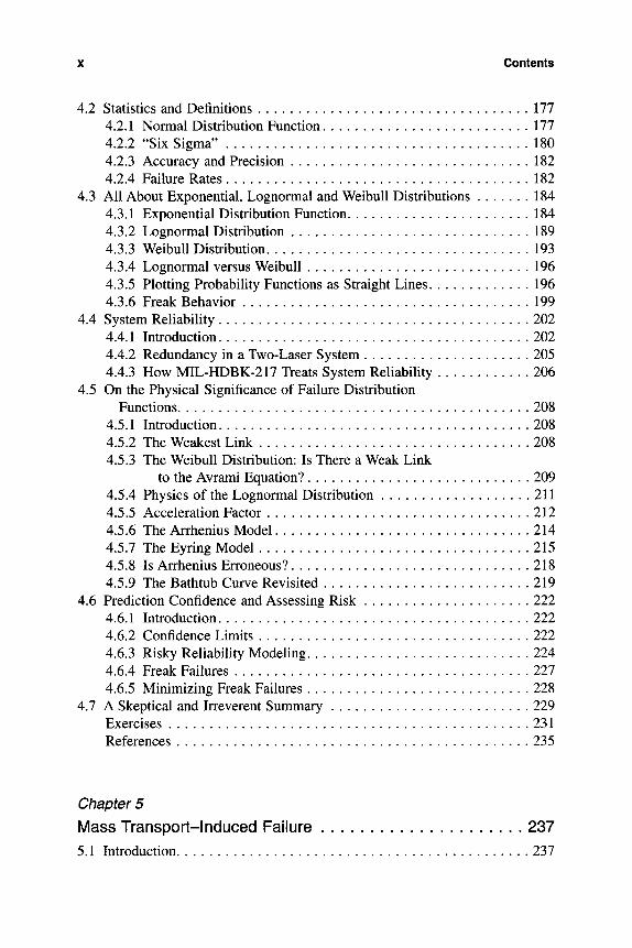
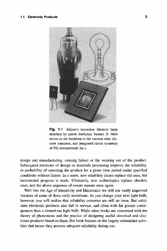
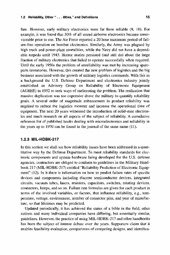
With the ability to generate electromagnetic waves around the turn of the cen-tury, the era of vacuum electronics was bom. The invention of vacuum tubes enabled electric waves to be generated, transmitted, detected, and amplified, making wireless communication possible. In particular, the three-electrode vac-uum tube invented by Lee de Forest in 1906 became the foundation of electron-ics for the first half of the twentieth century (5). Throughout the second half of the twentieth century, electronics has been transformed both by the transistor, which was invented in 1947, and integrated circuits (IC), which appeared a decade later. The juxtaposition of these milestone devices in Fig. 1-1 demon-strates how far we have come in so short a time.
A pattern can be discerned in the development of not only electrical devices and equipment, but all types of products. First, the genius of invention envisions a practical use for a particular physical phenomenon. The design and analysis of the components and devices are then executed, and finally, the materials and manufacturing processes are selected. Usage invariably exposes defects in
1.1 Electronic Products
Fig. 1-1 Edison's horseshoe filament lamp sketched by patent draftsman Samuel D. Mott serves as the backdrop to the vacuum tube, dis-crete transistor, and integrated circuit (courtesy of FSI International, Inc.).
design and manufacturing, causing failure or the vacating out of the product. Subsequent iterations of design or materials processing improve the reliability, or probability of operating the product for a given time period under specified conditions without failure. In a sense, new reliability issues replace old ones, but incremental progress is made. Ultimately, new technologies replace obsolete ones, and the above sequence of events repeats once again.
Well into the Age of Electricity and Electronics we still use vastly improved versions of some of those early inventions. As you change your next light bulb, however, you will realize that reliability concerns are still an issue. But solid-state electronic products also fail in service, and often with far greater conse-quences than a burned-out light bulb. While other books are concerned with the theory of phenomena and the practice of designing useful electrical and elec-tronic products based on them, this book focuses on the largely unheralded activ-ities that insure they possess adequate reliability during use.
4 An Overview of Electronic Devices and Tlieir Reliability
1.1.2 Solid-state Devices
The scientific flowering of solid-state device electronics has been due to the syner-gism between the quantum theory of matter and classical electromagnetic theory. As a result, our scientific understanding of the behavior of electronic, magnetic, and optical materials has dramatically increased. In ways that continue undiminished to the present day, exploitation of these solid-state devices, particularly semiconduc-tors, has revolutionized virtually every activity of mankind, e.g., manufacturing, communications, the practice of medicine, transportation, and entertainment (6).
Before focusing on electronics it is worth noting parallel developments in the field of photonics. The latter has been defined as "the technology for generating, amplifying, detecting, guiding, modulating, or modifying by nonlinear effects, optical radiation, and applying it from energy generation to conmiunication and information processing" (7). Building on the theoretical base laid by Maxwell, Planck and Einstein, opto-electronics (or electro-optics) applications include lasers, fiber optics, integrated optics, acousto-optics, nonlinear optics, and opti-cal data storage. Destined to merit a historical age of its own, photonics is pro-jected to dominate applications, as fundamental physical limits to electronic function are reached.
As already noted, two major revolutions in electronics occurred during the time from the late 1940s to the 1970s. In the first, transistors replaced vacuum tubes. These new solid-state devices, which consumed tens of milliwatts and operated at a few volts, eliminated the need for several watts of filament heater power and hundreds of volts on the tube anode. The second advance, the invention of the integrated circuit (IC) in 1958, ushered in multidevice chips to replace discrete solid-state diodes and transistors. Early solid-state devices were not appreciably more reliable than their vacuum tube predecessors, but power and weight savings were impressive. While discrete devices were advantageously deployed in a wide variety of traditional electronics applications, information processing required far greater densities of transistors. This need was satisfied by ICs.
1.1.3 Integrated Circuits
1.1.3.1 Applications Starting in the early 1960s the IC market was based primarily on bipolar transistors. Since the mid 1970s, however, ICs composed of metal-oxide-silicon (MOS) field effect transistors prevailed because they pos-sessed the advantages of device miniaturization, high yield, and low power dis-sipation. (Both bipolar and MOS transistors will be discussed in Chapter 2.) Then in successive waves, IC generations based on these transistors arose, flow-ered, and were superseded by small scale integration (SSI), medium scale inte-gration (MSI), large scale integration (LSI), and very large scale integration
1.1 Electronic Products 5
(VLSI). The latter, consisting of more than 10^ devices per chip, is giving way to ultra large scale integration (ULSI). In the early 1970s, sales of ICs reached $1 billion; in the year 2000, digital MOS ICs are projected to dominate a market worth about $100 billion; likewise, the broader market for electronic equipment is expected to climb at a rate in excess of 10% a year to a trillion dollars.
Integrated circuits are pervasive in computers, consumer goods, and conmiu-nications, where the total demand for each is roughly the same. Worldwide IC revenues are currently 32%, 30%, and 27% in these three sectors, respectively, with an additional 9% accounted for by industry and 2% by the military (7). The role of the computer industry and defense electronics as driving forces for IC production has been well documented. Less appreciated is the generally equal and at times even more powerful stimulus provided by consumer electronics in fostering the IC revolution.
Consumer products are those purchased by the individual or a family unit. Calculators, wristwatches, computers, cordless phones, answering machines, TVs, VCRs, audio systems, smoke detectors, and automobiles are examples that contain ICs. The automobile is an interesting case in point. There are presently more than 25 microprocessor IC chips in cars to control engine igni-tion timing, gas-air mixtures, idle speed, and emissions, as well as chassis sus-pension, antiskid brakes, and four-wheel steering. Furthermore, more recent trends will make vehicles intelligent through special application-specific ICs (ASICs) that provide computerized navigation and guidance assistance on high-ways, stereo vision, and electronic map displays. Advances in one sector of applications ripple through others. Thus TV phones and conferencing, multi-media computers, and digital high-definition television will no doubt permeate the consumer marketplace.
The Bell Labs News issue of February 7, 1997, marking the 50-year anniver-sary of the invention of the transistor, roughly estimates that "there are some 200 million billion transistors in the world today—about 40 million for every woman, man, and child." In the U.S. alone more than 200 ICs are used per household. The transistor count is rapidly swelling as the standard of living rises in China and India. With some five billion humans on earth there is much room for continued expansion of IC consumption in Third World countries. What is remarkable is how inexpensive the fruits of this technology have become. In the 1950s, the cost of a transistor dropped from $45 to $2. Today's transistors cost less than a hundred-thousandth of a cent each!
1.1.3.2 Trends Meeting the needs of burgeoning markets for digital elec-tronic products has necessitated a corresponding growth in the number of tran-sistors and complexity of the integrated circuits that house them. To gain a
6 An Overview of Electronic Devices and Tlieir Reliability
perspective of IC chip progress made in the 37 years from their inception to 1994, the time span analyzed, consider the following measures of advance (8):
1. Minimum feature size (F) has decreased by a factor of 50. 2. Die area (D^) has increased by a factor of approximately 170. 3. Packing efficiency (PE), defined as the number of transistors per minimum
feature area, has multiplied by over 100.
The composite number of transistors per chip A is the product of these three terms, orN= F'^ xD^x PE. Substitution indicates a staggering increase by a fac-tor of close to 5 X 10 , a number that may be compared to Moore's Law. In the mid 1970s, Gordon Moore, a founder of Intel, observed an annual doubling of the tran-sistor count rate, which held true for about 15 years until about 1990, and a reduc-tion in the rate of increase to 1.5 per year since then. By the end of the twentieth century a staggering one billion devices per chip may be anticipated. Moore prob-ably overstated the progress made, which is, nevertheless, extraordinarily impres-sive. In view of the fact that the price of chips has not changed appreciably, while their reliability has considerably improved over this time, these phenomenal advances are unprecedented in technological history.
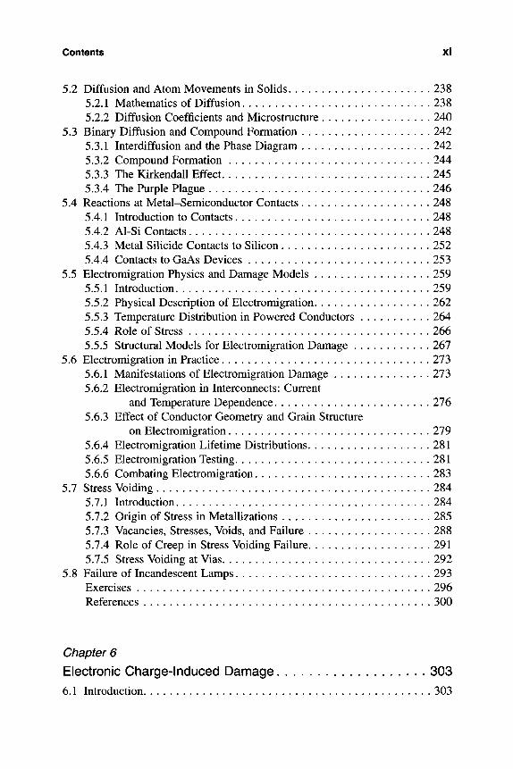
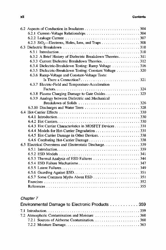
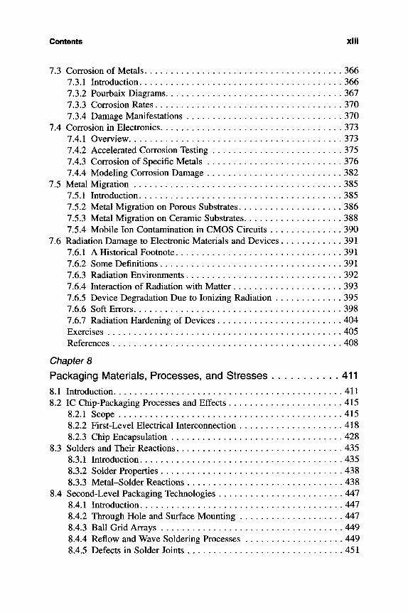
Both microprocessor and memory chips are the indispensable drivers of com-puter technology. Microprocessor ICs perform the numerous logic functions in circuits, while memory chips essentially store the information generated. The families of microprocessors fall into two categories—CISC (complex instruc-tion set computer) and RISC (reduced instruction set computer). Whereas CISC is well adapted to handle a diverse range of tasks, RISC reduces the number of instructions in favor of improved efficiency. Because of its ability to operate at high speed with low power consumption, most portable telecommunications equipment now employs RISC technology. Trends showing rapidly increasing transistor numbers in IC chips are presented in Fig. 1-2. When coupled with the far slower growth in chip size over the years (Fig. 1-3) one can begin to appre-ciate the huge growth in device density and the magnitude of feature shrinkage required to make it possible. Increasing the transistor count improves micro-processor performance as gauged by the number of instructions executed per second. Measured in MIPS (million instructions per second). Fig. 1-4 reveals a hundredfold increase in performance every 10 years.
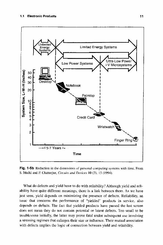
It is instructive to quantitatively sketch the time evolution of high-tech con-sumer electronics in terms of product size. In the past decade, for example, the overall volume of mobile communications and personal computers has been reduced by an order of magnitude or more, as shown in Figs. l-5a and l-5b; cor-responding weight savings have also been realized. It has been estimated that if a 1997 model digital cell phone contained vacuum tubes instead of transistors, it
1.1 Electronic Products
1G
100M 4
1K
* -i
• • • > •*•
Fj^entiumjJ?!;* 80686? ' Jff- ^ I
^-- Mitsubishi ^Gate Array
"80486 T T "
80786?
LSI Logic -"p----56k/^0386: : : : : '^ateArray••l";-;;-
168020 • T - " I -t t •• • r*""'
f^::!Vf 68000 SEqEElE^^^^
—•» - -t ^/%ES8085: |f^080 ;;r;;;-j;;;;;;;[;; . . . , ._ ,_
i I r : Ji^ = Microprocessor/Logic •[ .X.-....i... 400.4
\—i f i A = Memory (DRAM) j
n — I — r — 1 — I — I — r I — P -
70 72 74 76 78 80 82 84 86 88 90 92 94 96 98 Year
Fig. 1-2 Plot of the time-dependent increase in number of transistors on micro-processor and memory integrated circuit chips. Source: ICE Corp. 1993 Status.
would be larger than the Washington Monument! This volume reduction is pos-sible because of the increasing power of integrated circuits.
The source of these advances has been our ability to shrink the dimensions of critical device features. As a dramatic example of this, consider the width of alu-minum interconnections in the high-device-density IC chips shown in Fig. 1-6. The indicated dimensions have shrunk over the years from several microns to 0.35 |im presently. By 2010, conductor line widths of 0.07 |im are projected. More will be said about shrinkage of other device features throughout the book, and trends will be summarized in Chapter 12.
Each increase in packing density introduces a variety of new quality and reli-ability issues associated with specific devices, and more importantly. With the
An Overview of Electronic Devices and Their Reliabiilty
2,000
• T — 1 1 1 1 1 1 1 1 1 r
70 72 74 76 78 80 82 84 86 88 90 92 94 96 98 Year
Fig. 1-3 Plot of the time-dependent increase in chip area of microprocessor and memory integrated circuit chips. Source: ICE Corp. 1993 Status.
rapidly increasing number of contacts, interconnections, and solder joints. Reduced dimensions have made circuits increasingly sensitive to more subtle defects that had not previously threatened chip reliability. Confounding physical intuition, IC chip reliability as measured by the number of circuit failures has, in fact, dramatically increased over the last two decades. As revealed by Fig. 1-7, the number of failures in FITs (1 failure in 10^ hours of service = 1 FIT) has been reduced by a factor of 10 in this same period of time. Shown are the long-term failure rates as well as those that occur shortly after use conmiences, i.e., infant mortality (see Section 1.3.8). These remarkable reliability trends will probably continue in response to both customer needs and stiff competition, which have aggressively forced manufacturing to reduce the number of defects.
1.1 Electronic Products
MIPS
1000
100
10
68000 ^.
1980
68020
1985 1990 1995
Fig. 1-4 Microprocessor performance measured in MIPS. The 68000 series IC chips are trademarks of Motorola Inc. R3000 and R4000 are trademarks of MIPS Computer Systems Inc. Power 601 and Power 602 are trademarks of IBM. The 386, 486, and Pentium are trademarks of Intel Corp. SPARC is a registered trademark of SPARC International Inc. From I. Akitake and Y. Asano, Hitachi Review 44 (6), 299 (1995).
1.1.4 Yield of Electronic Products
Before we can derive the benefits of electronic products, they must first be man-ufactured in satisfactory numbers. Ideally, one might naively hope that after carefully processing a wafer containing a large number of integrated circuits, all would function properly when tested. In reality, however, the number of good, or functional, circuits may range from close to zero for a new technology to almost 100% for a mature technology where the "bugs" have been worked out. The very important term yield refers to the fraction of successful products that sur-vive final screening and meet specifications relative to the total number that started out to be processed or manufactured. Yield is essentially the bottom-line concern of manufacturing technology. In general, yields are never 100% because of some combination of problems associated with circuit design, processing, and random defects. The first may simply be due to errors in circuit design, while the others usually result from lack of process control and contamination. Specific examples of each will be deferred until Chapter 3.
10 An Overview of Electronic Devices and Their Reliability
4200 ml/4.1 kg
Miniaturization
Fig. 1-5a Reduction in the volume of wireless communications systems with time. From Y. Hishida and M. Kazama, Hitachi Review 42, 95 (1993).
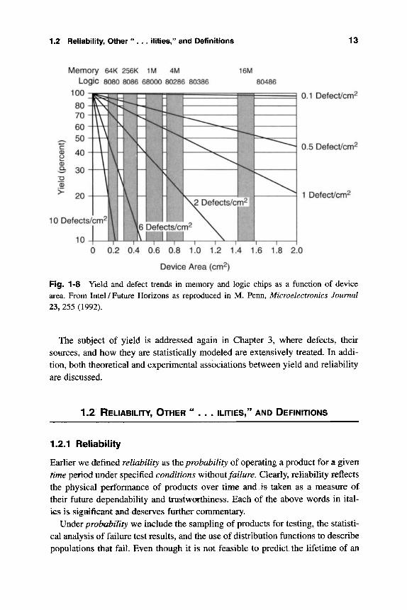
An excellent way to appreciate the broader factors that influence yield is through study of Fig. 1-8. The first important conclusion that can be drawn is that yield drops as the chip area increases. Secondly, for chips of a given area the highest yields occur for those that have the fewest defects. Here we note that every new generation of memory and logic chips invariably means an increase in device area. In DRAM memory chips, for example, increasing the capacity to 64 megabit (64Mb) implies a die size of roughly 2.6 cm^. This means that many fewer defects per unit area can be tolerated if the same yield level is to be achieved in successive generations of product. Simultaneously, the defect that signifies outright die rejection if present, the so-called "killer defect," becomes smaller and smaller in size because device features have shrunk in size. What aggravates the problem considerably is that process complexity increases as the device count rises. Whereas 1 Mb DRAMs require over 300 process steps, more than 500 steps are necessary for 64 Mb DRAM production. The chance of incor-porating defects is thus proportionately raised.
1.1 Electronic Products 11
0) N
(Ji E
Limited Energy Systems
Low Power Systems
10 9 8 7 6 5 4
Ultra-Low Power i-V Microsystems
Notebook
"^v Palmtop
V
Credit Card
Wristwatch c h ^
=lingC^^ JL
Finger Ring^ —L
-\ 5-7 Years I-
Time
Fig. 1-5b Reduction in the dimensions of personal computing systems with time. From S. Malhi and P. Chatterjee, Circuits and Devices 10 (3), 13 (1994).
What do defects and yield have to do with reliability? Although yield and reli-ability have quite different meanings, there is a link between them. As we have just seen, yield depends on minimizing the presence of defects. Reliability, an issue that concerns the performance of "yielded" products in service, also depends on defects. The fact that yielded products have passed the last screen does not mean they do not contain potential or latent defects. Too small to be troublesome initially, the latter may prove fatal under subsequent use involving a stressing regimen that enlarges their size or influence. Their mutual association with defects implies the logic of connection between yield and reliability.
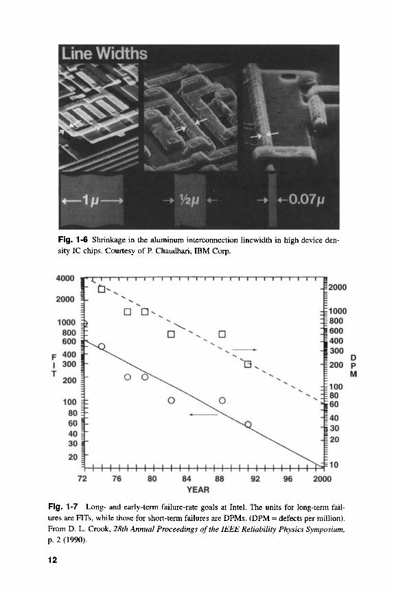
Fig. 1-6 Shrinkage in the aluminum interconnection linewidth in high device den-sity IC chips. Courtesy of P. Chaudhari, IBM Corp.
4000
Fig. 1-7 Long- and early-term failure-rate goals at Intel. The units for long-term fail-ures are FITs, while those for short-term failures are DPMs. (DPM = defects per milHon). From D. L. Crook, 28th Annual Proceedings of the IEEE Reliability Physics Symposium, p. 2 (1990).
12
1.2 Reliabilify, Other " . . . ilities," and Definitions 13
Memory 64K 2S6K 1M 4M Logic 8G80 8086 68000 80286 80386
100 80
16M 80486
0.1 Dafect/cm2
0.5 Defect/cm^
1 Defect/cm^ I 1 i \ I I 11 I Defects/cm^ I I
10 Defects/cm2
10 0 0.2 0.4 0.6 0.8 1.0 1.2 1.4 1.6 1.8 2.0
Device Area (cm^)
Fig. 1-8 Yield and defect trends in memory and logic chips as a function of device area. From Intel/Future Horizons as reproduced in M. F&nny Microelectronics Journal 23, 255 (1992).
The subject of yield is addressed again in Chapter 3, where defects, their sources, and how they are statistically modeled are extensively treated. In addi-tion, both theoretical and experimental associations between yield and reliability are discussed.
1.2 RELiABiLm^ O T H E R ILITIES," AND DEFINIT IONS
1.2.1 Reliability
Earlier we defined reliability as the probability of operating a product for a given time period under specified conditions without failure. Clearly, reliability reflects the physical performance of products over time and is taken as a measure of their future dependability and trustworthiness. Each of the above words in ital-ics is significant and deserves furthjer commentary.
Under probability we include the sampling of products for testing, the statisti-cal analysis of failure test results, and the use of distribution functions to describe populations that fail. Even though it is not feasible to predict the lifetime of an
14 An Overview of Electronic Devices and Their Reliabiiity
individual electronic component, an average lifetime can be estimated based on treating large populations of components probabilistically. Interestingly, projec-tions of future behavior can often be made without specific reference to the under-lying physical mechanism of degradation.
The time dependence of reliability is implied by the definition, and therefore the time variable appears in all of the failure distribution functions that will be subsequently defined. Acceptable times for reliable operation are often quoted in decades for communications equipment; for guided missiles, however, only min-utes are of interest. The time dependence of degradation of some measurable quantity such as voltage, current, strength, or light emission is often the cardinal concern, and examples of how such changes are modeled are presented through-out the book.
Specification of the product testing or operating conditions is essential in pre-dicting reliability. For example elevating the temperature is the universal way to accelerate failure. It therefore makes a big difference whether the test tempera-ture is 25°C, -25°C, or 125°C. Similarly, other specifications might be the level of voltage, humidity, etc., during testing or use.
Lastly, the question of what is meant by failure must be addressed. Does it mean actual fracture or breakage of a component? Or does it mean some degree of performance degradation? If so, by how much? Does it mean that a specification is not being met, and if so, whose specification? Despite these uncertainties it is generally accepted that product failure occurs when the required function is not being performed. A key quantitative measure of relia-bility is the failure rate. This is the rate at which a device or component can be expected to fail under known use conditions. More will be said about failure rates in Chapter 4, but clearly such information is important to both manufac-turers and purchasers of electronic products. With it, engineers can often pre-dict the reliability that can be expected from systems during operation. Failure rates in semiconductor devices are generally determined by device design, the number of in-line process control inspections used, their levels of rejection, and the extent of postprocess screening.
1.2.2 A Brief History of Reliability
Now that various aspects of reliability have been defined, it is instructive to briefly trace their history with regard to the electronics industry. In few applica-tions are the implications of wnreliability of electronic (as well as mechanical) equipment as critical as they are for military operations. While World War I reflected the importance of chemistry. World War II and all subsequent wars clearly capitalized on advances in electronics to control the machinery of war-
1.2 Reliability, Other " . . . ilitles," and Definitions 15
fare. However, early military electronics were far from reliable (9, 10). For example, it was found that 50% of all stored airborne electronics became unser-viceable prior to use. The Air Force reported a 20 hour maximum period of fail-ure-free operation on bomber electronics. Similarly, the Army was plagued by high truck and power-plant mortalities, while the Navy did not have a depend-able torpedo until 1943. Horror stories persisted (and still do) about the large fraction of military electronics that failed to operate successfully when required. Until the early 1950s the problem of unreliability was met by increasing spare-parts inventories. However, this created the new problem of logistics and the big business associated with the growth of military logistics commands. With this as a background the U.S. Defense Department and electronics industry jointly established an Advisory Group on Reliability of Electronic Equipment (AGREE) in 1952 to seek ways of meliorating the problem. The realization that massive duplication was too expensive drove the military to quantify reliability goals. A several order of magnitude enhancement in product reliability was required to reduce the logistics monster and increase the operational time of equipment. The next 20 years witnessed the introduction of solid-state electron-ics and much research on all aspects of the subject of reliability. A cumulative reference list of published books dealing with microelectronics and reliability in the years up to 1970 can be found in the journal of the same name (11).
1.2.3 MIL-HDBK-217
In this section we shall see how reliability issues have been addressed in a quan-titative way by the Defense Department. To meet reliability standards for elec-tronic components and system hardware being developed for the U.S. defense agencies, contractors are obliged to conform to guidelines in the Military Hand-book 217 (MIL-HDBK-217) entitled "ReHability Prediction of Electronic Equip-ment" (12). In it there is information on how to predict failure rates of specific devices and components including discrete semiconductor devices, integrated circuits, vacuum tubes, lasers, resistors, capacitors, switches, rotating devices, connectors, lamps, and so on. Failure rate formulas are given for each product in terms of the involved variables, or factors, that influence reliability, e.g., tem-perature, voltage, environment, number of connector pins, and year of manufac-ture, so that lifetimes may be predicted.
Updated periodically, it has achieved the status of a bible in the field; other nations and many individual companies have differing, but essentially similar, guidelines. However, the practice of using MIL-HDBK-217 and other handbooks has been the subject of intense debate over the years. Supporters claim that it enables feasibility evaluation, comparisons of competing designs, and identifica-
16 An Overview of Electronic Devices and Their Relialiility
tion of potential reliability problems. Detractors, and they are probably in the majority and certainly more vociferous, maintain that MIL-HDBK-217 reliability predictions do not compare well with field experience and generally serve to sti-fle good engineering judgment. Encyclopedic in its coverage of practical reliabil-ity concerns, examples of its use coupled with a discussion of its validity will be deferred to Chapter 4. Further information on this handbook can be obtained by contacting the Rome Laboratory RL/ERSR, Griffiss Air Force Base, NY 13441.
1.2.4 Long-Term Nonoperating Reliability
We can all appreciate that electrical products might suffer reliability problems as a result of service. But what are we to make of products that are stored in a non-operating condition for long periods of time, and then fail when turned on. Equipment that is not in direct use is either in a state of dormancy or storage. Dormancy is defined as the state in which equipment is connected and in an operational mode but not operating. According to this definition, dormancy rates for domestic appliances, professional and industrial equipment, and transporta-tion vehicles may be well over 90%. On the other hand, equipment that is totally inactivated is said to be in storage; such products may have to be unpacked, set up, and connected to power supplies to become operational. The consequences of nonfunctioning electrical equipment can be severe in the case of warning sys-tems that fail to protect against fire, nuclear radiation, burglary, etc. when called into service unexpectedly. Military success on the battlefield can hang in the bal-ance because of such failure to function.
The above are all examples of nonoperating reliability, the subject of a recent book by Pecht and Pecht (13). These authors contend that what are usually understood to be relatively benign dormant and storage environments for elec-tronics may, in fact, be quite stressful. Frequent handling, relocating and trans-port of equipment, and kitting (packing products in kits) as well as unkitting are sources of impact loading, vibration, and generally harmful stresses. An entirely quiescent environment, involving no handling at all, has even proven deleterious to some products. The materials within the latter are often not in chemical or mechanical equilibrium after processing, and residual stresses may be present. Like a compressed spring that naturally tends to uncoil, the material approaches equilibrium through atomic diffusion or mechanical relaxation processes. Bat-tery corrosion due to current leakage is a prime example of this kind of degra-dation. Less common examples include failure of presoldered components and open circuiting of integrated circuits (IC), both while being stored on the shelf prior to final assembly into electronic products. The former is due to the lack of solderability, presumably because of oxidation, during aging on the shelf. In the
1.3 Failure Physics 17
latter case, the vexing phenomenon of stress voiding results in slit-like crack for-mation in the aluminum grains of interconnections, causing ICs to fail. This effect, attributed to internal stress relief, is aggravated when current is passed through the chip. Stress voiding will be discussed more fully in Chapter 5.
With few exceptions the environments electronic products are exposed to in operational, dormant, and storage modes are not very different. The primary dif-ference is accelerated damage due to the influence of applied electric fields, the currents that flow, and the temperature rise produced. Several authors have pro-posed a correlation between the operating and nonoperating reliabilities of elec-tronics. A multiplicative factor ''FC' defining the ratio of these respective failure rates has been suggested. Values o f^ ranging anywhere from 10 to 100 have been reported. Such numbers appear to be little more than guesswork and have limited value. A more intelligent approach would be to extrapolate accelerated test results to conditions prevailing during dormancy and storage.
t.2.5 Availability, Maintainability, and Survivabitity
Important terms related to reliability but having different meanings are avail-ability, maintainability, and survivability. The first two refer to cases where there is the possibility of repairing a failed component. Availability is a measure of the degree to which repaired components will operate when called upon to perform. Maintainability refers to the maintenance process associated with retaining or restoring a component or system to a specified operating condition. In situations where repair of failures is not an option (e.g., in a missile), an appropriate mea-sure of reliability is survivability. Here, performance under stated conditions for a specified time period without failure is required. Normally these concepts are applied to the reliability of systems.
1.3 FAILURE PHYSICS
1.3.1 Failure Modes and Mechanisms; Reliable and Failed States
We now turn our attention to the subject of actual physical failure (or failure physics) of electronic devices and components, a concern that will occupy much of the book. At the outset there is a distinction between failure mode and failure mechanism that should be appreciated, although both terms have been used interchangeably in the literature. A failure mode is the recognizable elec-trical symptom by which failure is observed. Thus a short or open circuit, an
18 An Overview of Electronic Devices and Their Reliability
electrically open device input, and increased current are all modes of electrical failure. Each mode could, in principle, be caused by one or more different fail-ure mechanisms, however. The latter are the specific microscopic physical, chemical, metallurgical, environmental phenomena or processes that cause device degradation or malfunction. For example, open circuiting of an inter-connect could occur because of corrosion or because of too much current flow. High electric-field dielectric breakdown in insulators is another example of a failure mechanism.
Components function reliably as long as each of their response parameters, i.e., resistance, voltage, current gain, capacitance, have values that remain within specified design limits. Each of the response parameters in turn depends on other variables, e.g., temperature, humidity, semiconductor doping level, that define a multidimensional space consisting of reliable states and failed states. Failure consists of a transition from reliable to failed states (14). Irrespective of the specific mechanism, failure virtually always begins through a time-dependent movement of atoms, ions, or electronic charge from benign sites in the device or component to harmful sites. If these atoms or electrons accumulate in sufficient numbers at harmful sites, damage ensues. The chal-lenge is to understand the nature of the driving forces that compel matter or charge to move and to predict how long it will take to create a critical amount of damage. In a nutshell, this is what the modeling of failure mecha-nisms ideally attempts to do. A substantial portion of the latter part of the book is devoted to developing this thought process in assorted applications. Interestingly, there are relatively few categories of driving forces that are operative. Important examples include concentration gradients to spur atomic diffusion or foster chemical reactions, electric fields to propel charge, and applied or residual stress to promote bulk plastic-deformation effects. And, as we shall see, elevated temperatures invariably hasten each of these processes. In fact, the single most universally influential variable that accelerates damage and reduces reliability is temperature. Other variables such as humidity, stress, and radiation also accelerate damage in certain devices.
1.3.2 Conditions for Change
Much can be learned about the way materials degrade and fail by studying chemical reactions. As a result of reaction the original functional materials are replaced by new, unintended ones that impair function. Thermodynamics teaches that reactions naturally proceed when energy is reduced. Thus in the transition from reliable to failed behavior, the energies of reliable states exceed those of the failed states; furthermore, the process must proceed at an appreciable rate.
1.3 Failure Physics 19
Similarly, in chemical systems two conditions are necessary in order for a reac-tion to readily proceed at constant temperature and pressure:
1. First there is a thermodynamic requirement that the energy of the system be minimized. For this purpose the Gibbs free energy (G) is universally employed as a measure of the chemical energy associated with atoms or molecules. In order for a reaction to occur among chemical species the change in free energy (AG) must be minimized. Therefore, AG = Gf - Gi must be negative (AG < 0), where Gf is the free energy of the final (e.g., failed) states or products and Gi the free energy of the initial (e.g., rehable) states or reactants. When AG attains the most negative value possible, all of the substances present are in a state of ther-modynamic equilibrium. For chemical reactions thermodynamic data are often tabulated as AG, or in terms of its constituent factors, /SH (the enthalpy change), and A^ (the entropy change). These contributions are related by
AG = AH- TAS. (1-1)
Example 1-1 Consider the problem of selecting a contact material for a device made of the high-temperature superconductor YBa2Cu307. In addition to the usual attributes of low contact resistance, adhesion, matching of thermal expansion, etc., the contact must be chemically stable. Silver and aluminum are potential contact candidates. Which metal contact is likely to be more stable?
Answer We first make the assumption that AG ~ AH in Eq. 1-1 when TA " is small. This is generally true in the present case. Therefore, the criterion for pos-sible chemical reaction is that AH < 0. The reactions between Ag or Al and com-mon oxides of YBCO superconductors are given below. Using published enthalpies at 298K for the involved chemical species, the following AH29S val-ues are calculated for potential reactions between the contact metals and assorted superconductor oxides. In doing so we recall from elementary thermochemistry that the net enthalpy change is the sum of the enthalpies of the products minus the sum of enthalpies for the reactants, i.e., A//298(reaction) = E A//298 (products) - E AH29S (reactants).
Reaction
CU2O
(-40 kcal/mol)
Y2O3
(-450 kcaymol)
BaO
(-133 kcal/mol)
+
+
+
+
+
2Ag =
2(0)
8Ag =
8(0)
3Ag =
3(0)
= Ag20
(-7.3 kcal/mol)
= 3Ag20
3(-7.3 kcal/mol)
= Ag20
(-7.3 kcal/mol)
+
+
+
2Cu
2(0)
2AgY
2(-23.87 kcal/mol)
AgBa
(-20.05 kcal/mol)
Enthalpy
A//298 = +32.7 kcal
A7/298 = +380 kcal
A^298 = +106 kcal
20 An Overview of Electronic Devices and Their Reliability
f (-400 kcal/mol) AH298 = -109 kcal
CU20 +
(-40 kcal/mol)
Y2O3 +
(-450 kcaymol)
BaO +
(-133 kcal jmol)
fA. =
f(0) 2A1 =
2(0)
f A. =
f(0)
A1CU2
(-16.1 kcaymol)
AI2O3
(-400 kcal/mol)
]-Al203
^( -400 kcal/mol)
+
+
+
JAI2O3
y ( - 4 0 0
2Y
2(0)
Ba
(0)
AH298 = +50 kcal
A//298 = - 0 3 kcal
The positive enthalpy values for Ag mean that this metal is less reactive than Al and therefore likely to be a more stable contact.
2. The second requirement is a practical one that involves kinetics. Once the reaction is thermodynamically possible, it must proceed at an appreciable rate. Otherwise, there will be little actual chemical change and degradation. The rate at which chemical reactions occur is proportional to the Maxwell-Boltzmann factor (also known as the Boltzmann or Arrhenius factor) according to
Rate = A exp - ( " ^ T - ) ; A = constant (1-2)
where AG* is the activation free energy (in the usual units of J/mol or cal/mol), r i s the absolute temperature, and R is the gas constant (= 8.314J/mol-K or 1.987 cal/mol-K). Because of its ubiquitous presence whenever degradation is ther-mally accelerated, Eq. 1-2 is easily one of the most important equations in this book and one worth remembering.
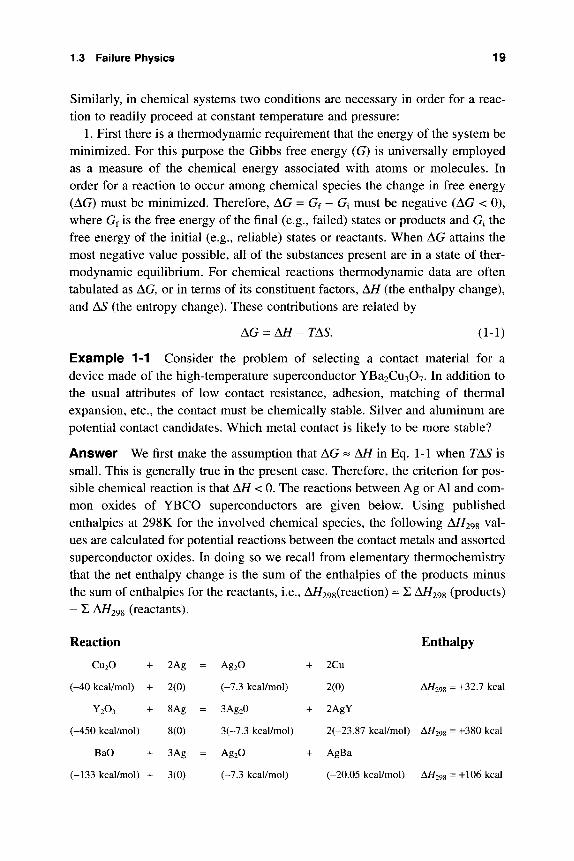
Note that AG* does not equal AG, and in fact has a very different interpreta-tion, as shown in Fig. l-9a. The energy barrier that atoms or molecules must sur-mount to squeeze by neighbors, or push them apart, so that reaction can occur is essentially AG*; its magnitude hinges on the particular path between initial (unstable) and final (stable) states. If a catalyst is present, AG* may be effec-tively reduced. In contrast, AG is the fixed energy difference between the final and initial states, irrespective of path.
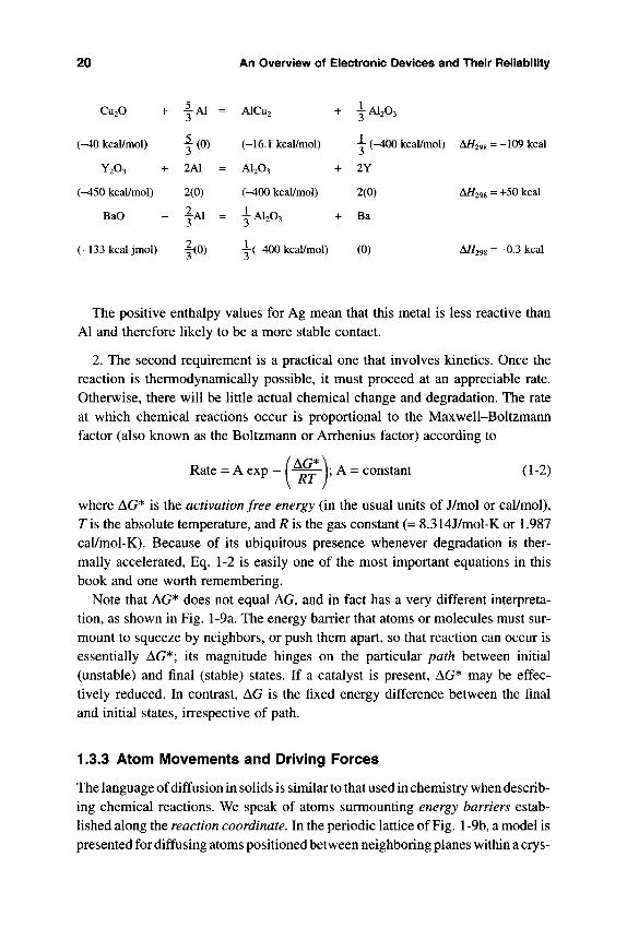
1.3.3 Atom Movements and Driving Forces
The language of diffusion in solids is similar to that used in chemistry when describ-ing chemical reactions. We speak of atoms surmounting energy barriers estab-lished along the reaction coordinate. In the periodic lattice of Fig. l-9b, a model is presented for diffusing atoms positioned between neighboring planes within a cry s-
1.3 Failure Physics 21
(a) FREE ENERGY
DISTANCE-
(C) FREE ENERGY. APPLIED FIELD
DISTANCE
Fig. 1-9a,C Potential energy of atoms in a periodic lattice: (a) in the absence of a force, (c) in the presence of a force (field). The energy barrier for reaction is AG*.
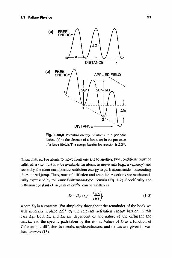
talline matrix. For atoms to move from one site to another, two conditions must be fulfilled; a site must first be available for atoms to move into (e.g., a vacancy) and secondly, the atom must possess sufficient energy to push atoms aside in executing the required jump. Thus, rates of diffusion and chemical reactions are mathemati-cally expressed by the same Boltzmann-type formula (Eq. 1-2). Specifically, the diffusion constant D, in units of cm^/s, can be written as
D = / ^ o e x p - ( ^ ^ , (1-3)
where DQ is a constant. For simplicity throughout the remainder of the book we will generally replace AG* by the relevant activation energy barrier, in this case ED. Both DQ and E^ are dependent on the nature of the diffusant and matrix, and the specific path taken by the atoms. Values of D as a function of T for atomic diffusion in metals, semiconductors, and oxides are given in var-ious sources (15).
22 An Overview of Electronic Devices and Their Reliability
ooo ooo ooo OoO oqp OOT)
vacancy
-e- a - . -
Fig. 1 -9b Model of a diffusing atom jumping between neighboring plane sites into a vacancy. From reference 15.
Now we consider the transport of atoms in systems where generalized driving forces exist. If a driving force or bias did not exist in the case of diffusion, atoms would migrate with equal probability in opposite directions and there would be no net displacement. When driving forces (or fields) exist over atomic dimen-sions a, the periodic array of lattice energy barriers assumes a tilt, or bias, as shown in Fig. l-9c. Now, atoms in site 2 have a lower energy by an amount AG than those in site 1, a distance a away. In addition, the energy barrier to atomic motion from 1 to 2 is lower than that from 2 to 1. In fact, the slope of G with distance, or the free energy gradient, is caused by and is physically equal to the applied driving force (F). This force effectively acts over distance a/2, so that F = 2AG/a with units of force/mol (or force/atom). Since atoms vibrate in place with frequency v (=10^^ s~ ) awaiting a successful jump, the rate at which atoms move to the right is given by
ri2 = V exp (AG*-AG)
RT (s-\ (l-4a)
1.3 Failure Physics 23
while in the latter case,
21 = ^ ^^P (AG* + AG)
RT (s-'y (l-4b)
The net rate, or difference of individual rates, is the quantity of significance, and it is given by
^net = ^12 - ^21 = V CXp AG* RT
2 sinh AG RT
(1-5)
It is instructive to consider the case where AG* > AG If additionally, AG is small compared to RT, sinh AG/RT ^ AG/RT. After substituting AG = Fa/2 and noting that the atomic velocity w = a Tnet, Eq. 1-5 becomes
DF RT'
(1-6)
where D is associated with a\ exp [- AG'^/RT] (or a\ exp [-Eo/RT]. This important formula is known as the Nernst-Einstein equation and is valid
in describing both chemical and physical change induced through diffusional motion of atoms. It is to the dynamics of microscopic chemical systems what Newton's law relating force to acceleration is to macroscopic mechanical sys-tems. Later we will model degradation phenomena like electromigration, mechanical creep, and compound growth using this equation. When the driving force is large, however, the higher powers of sinh AG/RT cannot be neglected. Atomic velocities or rates of reaction may then vary as the hyperbolic sine or some power p of the driving force, i.e., F^. Alternatively, it is common to absorb AG, or the driving forces, into AG*, so that in effect a reduced activation energy is operative. As a result, hybrid expressions of the general form
= KF^ exp (AG*-aF)
RT (1-7)
{K = constant) are sometimes used in modeling high field damage or phenomena (e.g., dielectric breakdown, high electric-field conduction in insulators). The mean time to failure (MTTF) is usually assumed to be proportional to the recip-rocal of the degradation reaction velocity, i.e., MTTF ~ v~\
It is common to have more than one operative driving force acting in concert with temperature to speed reactions. Note that temperature is not a true driving force, even though terms like "temperature stressing" are frequently used; true driving forces like temperature gradients establish a system bias. Electric fields, electric currents, mechanical stress, and humidity gradients are examples of forces that have served to hasten failure of components and devices. Empirical formulas
24 An Overview of Electronic Devices and Their Reliabiiity
combining products of forces and modified Boltzmann factors (e.g. , . . . F * F /^ . . . , . , . exp [- (AG* - aFi - bFj... )/RT might, for example, be used to account for dielectric breakdown at a given electric field (F ) and humidity level (Fj),
Whether small or large driving forces are operative is dependent on the phys-ical process in question. Small energy changes, corresponding to bond shifting, or breaking and reforming in a single material, are involved in diffusion, grain growth, and dislocation motion. This contrasts with chemical reactions, for example, where high-energy primary bonds break in reactants and re-form in products.
1.3.4 Failure Times and the Acceleration Factor
At the outset it is important to distinguish among the various times that are asso-ciated with failure. Imagine a number (n) of products that fail in service after successively longer times ti, t2, tj, 4, 5, . . . f„. The mean time to failure is sim-ply defined as
n
This time, however, differs from the median time to failure ( 59), which is defined to occur when 50% have failed; thus half of the failures happen prior to /50 and the remaining half after t^Q. Lastly, there is the mean time between fail-ures, or MTBF, defined as
MTBF = ^^' ~ ' + ( 3 - 2) + • • • + {K - f„_i) j_g^ n
In this book we shall usually use MTTF to describe or model physical failure times. On the other hand, /50 will mostly arise in the statistical or mathematical analysis of failure distributions.
In the reliability literature there is a widely used term known as the accelera-tion factor (AF) that is based on explicit formulas for failure rate, failure time, or the Nemst-Einstein equation in its various versions and modifications. AF is defined as the ratio of a degradation rate at an elevated temperature T2 relative to that at a lower base temperature Ti, or conversely, as the ratio of times to fail-ure at Ti and T2. Through application of Eq. 1-2, the acceleration factor is easily calculated in the temperature range between Ti and T2:
MTTF(T2) exp[AG*/RT2] ^ [\ R J \Ti Ti)]
1.3 Failure Physics 25
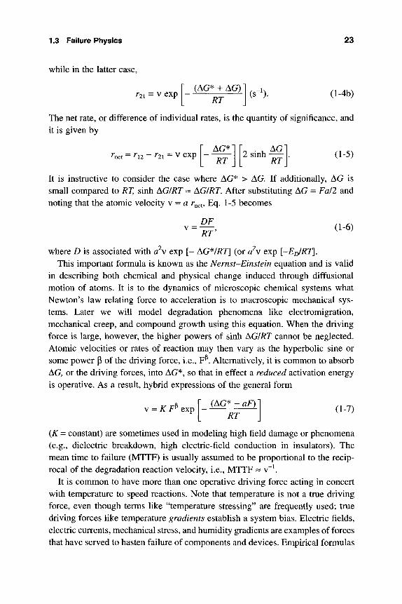
Thus if the failure time is known at T2, then it can also be calculated at Ti. Addi-tionally, these Arrhenius expressions can be used to determine the activation energy if AF is known. In the days before computers, a manual Arrhenius slide-rule calculator for AF was devised and is shown in Fig. 1-10. With it relation-ships among the ratio of reaction rates, the two involved temperatures, and the activation energy are readily displayed.
When one driving force having magnitudes Fj and F2 is operative at the two temperatures, we may tacitly assume that degradation reaction rates proceed with the velocity given by Eq. 1-6. With such an assumption the acceleration factor is given by
AF = MTTFcro
(ri/Fi) exp
{T2IF2) exp
RTi\
RT2\
7\F2
T2F1 exp R [T,
J_ T2
(1-11)
We shall return to acceleration factors in Section 4.5.5.
1.3.5 Load-Strength Interference
An instructive way to close this section on reliability physics is to consider the concept of load-strength interference (16). Every product has a collection of individual strengths (Si) or stress levels of resistance to corresponding loads (L ) applied in service. Note that in the context of this discussion the loads are more
T.hT,hTH.i.i.'i.i.Li,l.i.i.l l i l i l i i I I I § § ? s o ^
i l i i i j l i i | i lmiljd, ij | i l i i i i l l l i i l i l i l i l i l i l i l i l i l [ 4 I|f|l|l|l|l|llll|ftlp|llll|fl'll|'l1l'
I I I i l l 11 I I I 1 ? i J I I i im'l I T ITITITLI
^ « ' «NHO» » « ' 0., o j 0.3 0.4 o j ..0 I S J J 4 s «
l i t n i i M Ill I II I I I ' l ' l ' l lM|W'milh| l | l | l | | t? . / , . - . ' J J 4 5 10 » I ARRHENIUS CALCULATOR I " ' J 4 5 K) SO 100 »» W* W K 1 ARRHENIUS CALCULATOR [
ij.l.hlllllll.l.l.lj J
l l l l l l l l l l l l l l l 1 1 I I I ^ SOIOO » • 10«IO« K- I
ACCiUIATION MCTOt l l t / l l ) •
^ R H E N I U S CALCULATOR is AM AID IN COMrUTme THE EFFECT OF TEMFEftATUHE ON THE RATE OF CttEIIICAl FKOCESSES. THE A C C E L E R A T I O N F A C T O R iS JUST THE RATIO { R a / R t ) OF THE REACTION RATES AT
TWO TEMPERATURES, T j AND T ] . THE " A C T I V A T I O N E N E R G Y " Q IS A MEASURE OF THE SEMSITIVITY OF
RATE TO TEMFERATURE. TWO Q S M I E S ARE FROVIOEO, SINCE TWO SYSTEMS OF UNITS FOR Q ARC COMMONIY USEO.
EXAMPLE: etVEN T, = 150'C, T2 » 25«C, FIND (Ra/R i ) 1. SET THE SHOE SO THAT 1 5 0 * C ON THE HIGHER TENFERATURE SCALE COINCIDES WITH 2 S ' ' C ON THE LOWER
TEMPERATURE SCALE.
2. READ ( A T / T ) T 2 l AT ARROW ( X ) . RESET THE SLIDE SO THE SAME VALUE IS INDiaTEO RY ( g )
S.REAO ( R ? / R j ) OPPOSITE A KNOWN VALUE OF Q ; OR, READ Q OPPOSITE A KNOWN VALUE OF { R j / R l )
IF SOTH Q ANO ( R l / R t ) ARE KNOWN, REVERSE THE PROCEDURE TO DETERMINE T | OR T j .
0«ti«n*d by A.T. ENOUSH
Fig. 1-10 Arrhenius calculator slide rule designed by A. English, AT&T Bell Lab-oratories.

26 An Overview of Electronic Devices and Their Reiiability
correctly applied stresses. Thus a ceramic has an ultimate tensile strength beyond which it fractures, a critical electric field level that causes breakdown, a specific resistance to thermal-shock loading, and so on. As long as the mechani-cal and electrical service loads challenge, but do not exceed, the respective strengths, the ceramic is safe. But, should any one of its strengths be exceeded by the corresponding load, the ceramic undergoes catastrophic failure by that particular mechanism.
These ideas are illustrated in Fig. 1-1 la, where the particular set of load and strength variables have discrete values. In this case the strength exceeds the load, and there is no failure. It is more realistic to assume that the strength of materials is statistically distributed, as shown in Fig. 1-1 lb and indicated on the vertical axis. For example, a given ceramic has a probability of failing over a wide distribution of tensile strength levels, while in metals that distribution is extremely narrow. Simi-larly, the applied loads are often not constant but distributed over a range of values. Since the magnitude of the statistically lowest strength level is significantly higher than the largest applied load by a large margin, failure is again impossible. With time, however, the strength of materials may wane due to degradation (e.g., thermal
X I-o z LU DC I -
< O
(a)
Fig. 1-11 (a) Discrete set of load and strength values. There is no failure because the strength exceeds the load, (b) Both strengths and loads are statistically distributed. With time at constant load, decreasing strength causes increasing overlap, or interference, and eventual failure.
1.3 Failure Physics 27
softening due to creep, corrosion), but the applied stress distribution still remains unchanged. Conditions for marginal behavior followed by failure may then arise because service load levels overlap or interfere with the strengths of the weaker members. This subject will be addressed again in Section 12.5.2.
1.3.6 Semiconductor Device Degradation and Failure
The mechanisms for semiconductor failure can be grouped into three main cate-gories (17):
1. Chip level or intrinsic failures 2. Packaging or extrinsic failures 3. Electrical stress (in-circuit) failures
Intrinsic failure mechanisms originate from the silicon chip or die and the pro-cessing done in the "front end" of manufacturing. Potential defects and sources for failure exist in each material used and in every process step that alters com-position and device features. Defect sources can reside in the silicon wafer sub-strate itself, dielectrics like Si02 and other insulating films (silicon nitride, phos-phorous, and boron-containing oxide glasses), the metallizations that include aluminum-base alloy film interconnections between devices and components, and the semiconductor contacts composed of assorted metal alloys and com-pounds (Al, Al-Si, various metal silicides, Ti-W, TiN, etc.). Design errors plus the combination of lithography (patterning) and processing defects, the ubiqui-tous presence of contamination, and the intrinsic limitations of material proper-ties all sow the seeds for eventual chip-level failures. Temperature, voltage, cur-rent, etc., stressing during use, combined with environmental influences such as humidity and radiation, then accelerate the transition from reliable to failed states. Mass-transport induced failure mechanisms on the chip include interdif-fusion that results in unwanted compounds, precipitates or void formation at contacts, electromigration or a current-induced migration of atoms in intercon-nections, and corrosion at unprotected contacts. Examples of deleterious charge transport effects include dielectric breakdown, penetration of Si02 by so-called "hot electrons" that originate in the underlying silicon, and "soft errors" in logic or memory caused by ionizing radiation. Chapters 5, 6, 7, and 10 address such failures in greater detail.
Extrinsic failures are identified with the interconnection and packaging of chips in the "back end" of manufacturing. Potential failures now arise in the steps associ-ated with ensuring that integrated circuit contact pads are electrically connected to external power sources and signal processing circuits. Problems arise in attaching dies to metal frames and wires to contact pads, encapsulating chips into packages.
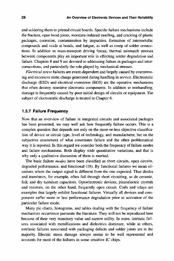
28 An Overview of Electronic Devices and Their Reiiability
and soldering them to printed circuit boards. Specific failure mechanisms include die fracture, open bond joints, moisture-induced swelling, and cracking of plastic packages, corrosion, contamination by impurities, formation of intermetallic compounds and voids at bonds, and fatigue, as well as creep of solder connec-tions. In addition to mass-transport driving forces, thermal mismatch stresses between components play an important role in effecting solder degradation and failure. Chapters 8 and 9 are devoted to addressing failure in packages and inter-connections, and particularly the role played by mechanical stresses.
Electrical stress failures are event-dependent and largely caused by overstress-ing and excessive static charge generated during handling in service. Electrostatic discharge (BSD) and electrical overstress (EOS) are the operative mechanisms that often destroy sensitive electronic components. In addition to mishandling, damage is frequently caused by poor initial design of circuits or equipment. The subject of electrostatic discharge is treated in Chapter 6.
1.3.7 Failure Frequency
Now that an overview of failure in integrated circuits and associated packages has been presented, we may well ask how frequently failure occurs. This is a complex question that depends not only on the more-or-less objective classifica-tion of device or circuit type, level of technology, and manufacturer, but on the subjective assessment of what constitutes failure and the often problematical way it is reported. In this regard we consider both the frequency of failure modes and failure mechanisms. Both display wide quantitative variations, and that is why only a qualitative discussion of them is merited.
The basic failure modes have been classified as short circuits, open circuits, degraded performance, and functional (18). By functional failures we mean sit-uations where the output signal is different from the one expected. Thus diodes and transistors, for example, often fail through short circuiting, as do ceramic, foil, and dry tantalum capacitors. Optoelectronic devices, piezoelectric crystals and resistors, on the other hand, frequently open circuit. Coils and relays are examples that largely exhibit functional failures. Virtually all devices and com-ponents suffer more or less performance degradation prior to activation of the particular failure mode.
Many pie charts, histograms, and tables dealing with the frequency of failure mechanism occurrence permeate the literature. They will not be reproduced here because of their very transitory value and narrow utility. In some, intrinsic fail-ures associated with metallizations and dielectrics dominate, while in others, extrinsic failures associated with packaging defects and solder joints are in the majority. Electric stress damage always seems to be well represented and accounts for most of the failures in some sensitive IC chips.
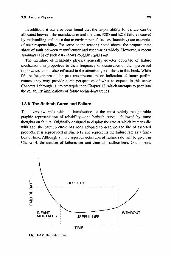
1.3 Failure Physics 29
In addition, it has also been found that the responsibihty for failure can be allocated between the manufacturer and the user. ESD and EOS failures caused by mishsuidling and those due to environmental factors (humidity) are examples of user responsibility. For some of the reasons noted above, the proportionate share of fault between manufacturer and user varies widely. However, a recent sunmiary (18) of such data shows roughly equal fault.
The literature of reliability physics generally devotes coverage of failure mechanisms in proportion to their frequency of occurrence or their perceived importance; this is also reflected in the attention given them in this book. While failure frequencies of the past and present are no indication of future perfor-mance, they may provide some perspective of what to expect. In this sense Chapters 1 through 11 are prerequisite to Chapter 12, which attempts to peer into the reliability implications of future technology trends.
1.3.8 The Bathtub Curve and Failure
This overview ends with an introduction to the most widely recognizable graphic representation of reliability—the bathtub curve—followed by some thoughts on failure. Originally designed to display the rate at which humans die with age, the bathtub curve has been adopted to describe the life of assorted products. It is reproduced in Fig. 1-12 and represents the failure rate as a func-tion of time. Although a more rigorous definition of failure rate will be given in Chapter 4, the number of failures per unit time will suffice here. Components
INFANT MORTALITY
WEAROUT
TIME
Fig. 1-12 Bathtub curve.
30 An Overview of Electronic Devices and Tlieir Reiiabiiity
and devices usually live through one or more stages of this curve. During early life the failure rate is high, since the weak products containing gross or macro-scopic manufacturing defects do not survive. This short-time portion of the curve is therefore known as the early failure, or more commonly as the infant mortality, region. Eliminating this region of the curve is effected by the widely employed practice of screening out obviously defective components, as well as weak ones with a high potential for failure. In such screening processes, prod-ucts must survive the ordeal of bum-in (e.g., stressing at high temperature, appli-cation of electrical overstress, temperature cycling) prior to shipment.
In contrast to the declining failure rate of infant mortality, the next region is characterized by a roughly constant failure rate. Since random failures occur that are not intrinsic to devices but rather to external circumstances (e.g., lightning, floods) during the indicated time span, this region normally corresponds to the working life of the components. Lastly, the failure rate increases in the last stages of life due to wearout. More subtle, microscopic defects grow over time, curtail-ing life in these latter stages. The reader will well appreciate that many mechani-cal components and biological systems seem to track similar life histories.
Approaches to achieving high reliability differ significantly in the infant mor-tality and wearout stages. In the former, the sources, or root causes, of defects must be exposed, followed by action to eliminate them. If defects cannot be eliminated at the source, then screening by bum-in is conducted. Wearout failure is combated by developing robust technologies with improved circuit and device designs that employ damage-resistant materials. Nowadays, integrated circuit chips rarely wear out; rather, new technology usually forces them into retire-ment. In Section 4.5.9 the bathtub curve will be revisited to capitalize on the sta-tistical functions introduced there.
Perhaps the three most important words raised about failure are when, how, and why\ in one form or other, the remainder of the book is largely devoted to addressing them. The connections between these terms are neatly depicted in the triangular representation of Fig. 1-13 (19). At the triangle's base we essentially have the divisions of the bathtub curve we have just considered. Corresponding failures can be gradual, the way soles on shoes wear, or sudden and catastrophic, such as when light-bulb filaments bum out. Failures can be random, say due to electrostatic discharge, or preordained, where some intemal mechanism causes the product to fail deterministically at a set rate from the moment of birth. Pre-ordained failures are thus time dependent. These descriptors may be directly related, as indicated by the solid lines, or show the absence of a connection in the case of a dashed line. Thus, wearout failures may be gradual or sudden, but not random. Infant failures display all characteristics, and this makes it difficult to deal with them.
1.4 Summary and Perspective 31
% \ HOW
MIDLIFE WEAR-OUT
PREMATURE
WHEN
Fig. 1-13 Depiction of connections between the when, why, and how of failures. From reference 19. Solid lines denote a connection, and dashed lines indicate the absence of a connection.
1.4 SUIVII\1ARY AND PERSPECTIVE
As its title suggests, this chapter has provided a brief overview of the reliability of electronic materials and devices. These important concerns are intimately tied to the performance of present electronic products as well as to the creation of improved successors. Repeated cycles of manufacture, field use, failure, product redesign, manufacture . . . . have characterized the Age of Electricity and Elec-tronics since its inception, and will probably be coterminous with its demise, if that ever occurs. Issues of defects, product yield, reliability, and degradation are important considerations in these cycles. In this chapter a broad footprint of these and related topics treated in the book has been broadly sketched.
Appreciation of the causal connections between the types electronic products and the way they fail requires an understanding of the nature of the materials they are composed of. Recommended texts on materials science and engineering (15, 20-22) will assist the reader to acquire this background. Next, the behavior of spe-cific devices (Chapter 2) and how they were processed with particular reference
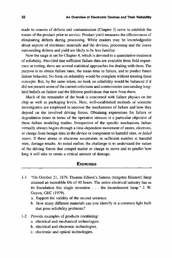
32 An Overview of Electronic Devices and Their Reliabiiity
made to sources of defects and contamination (Chapter 3) serve to establish the nature of the product prior to service. Product yield measures the effectiveness of eliminating defects during processing. While readers may be knowledgeable about aspects of electronic materials and the devices, processing and the issues surrounding defects and yield are likely to be less familiar.
Now the stage is set for Chapter 4, which is devoted to a quantitative treatment of reliability. Provided that sufficient failure data are available from field experi-ence or testing, there are several statistical approaches for dealing with them. The purpose is to obtain failure rates, the mean time to failure, and to predict future failure behavior. No book on reliability would be complete without treating these concepts. But, by the same token, no book on reliability would be balanced if it did not present some of the current criticisms and controversies surrounding long-held beliefs on failure and the lifetime predictions that stem from them.
Much of the remainder of the book is concerned with failure physics on the chip as well as packaging levels. Here, well-established methods of scientific investigation are employed to uncover the mechanisms of failure and how they depend on the involved driving forces. Obtaining expressions for failure or degradation times in terms of the operative stresses is a particular objective of these failure modeling studies. Irrespective of the specific mechanism, failure virtually always begins through a time-dependent movement of atoms, electrons, or charge from benign sites in the device or component to harmful sites, or failed states. If these atoms or electrons accumulate in sufficient number at harmful sites, damage results. As noted earlier, the challenge is to understand the nature of the driving forces that compel matter or charge to move and to predict how long it will take to create a critical amount of damage.
EXERCISES
1-1 "On October 21, 1879, Thomas Edison's famous (tungsten filament) lamp attained an incredible life of 40 hours. The entire electrical industry has as its foundation this single invention . . . the incandescent lamp." J. W. Guyon, GEC (1979). a. Support the validity of the second sentence. b. How many different materials can you identify in a common light bulb
that pose reliability problems?
1-2 Provide examples of products combining: a. electrical and mechanical technologies. b. electrical and electronic technologies. c. electronic and optical technologies.
1.4 Summary and Perspective 33
1-3 The law of personal computing systems scaling suggests that the logarithm of the sum of the length (L) plus width (W) plus height (H) varies lineariy with time. If L+W-^His halved every six years, sketch the variation for the following computers: desktop, notebook, palmtop, credit card, wrist watch, and finger ring. When can finger ring computers be expected?
1-4 The number of transistors used per person in the U.S. has grown from about 5 to 4 x 10^ during the years 1955-1997. Sketch this growth in usage on a graph using appropriate axes. If the trend continues, estimate the number of transistors each person will be using in 2010.
1-5 The growth in the number of devices per chip (N) appears to obey a law of the form dN/dt« kiV (k = constant), i.e., growth proportional to how many devices are instantaneously present. Chemical reactions and radioactive decay also suggest similar trends. Discuss physical reasons for the expo-nential rise or exponential decay.
1-6 Write an equation that approximates the decrease in size of mobile phones. In what year can we expect to see the Dick Tracy comics become reality by incorporating telephones into wristwatches? Assume that the watch dimensions are 3.5 cm x 3.5 cm x 1 cm.
1-7 The implications of unreliability in the medical profession are at least as severe as they are in aerospace technology. Comment on possible differ-ences and similarities in the reliability issues faced by each.
1-8 By considering Figures 1-2 and 1-3, calculate the density (nuinber per unit area) of devices as a function of time. Is the rate of growth in device den-sity higher in microprocessor or memory chips?
1-9 Comment on the thermodynamic stability of silicon, aluminum, and silicon dioxide that are often either in contact with or located within a few nanometers of each other on integrated circuit chips.
1-10 Contrast the shape of the bathtub curve for human death rates with age in 1900 with that at the end of the twentieth century. What are the reasons for the difference?
1-11 The energy barrier that must be surmounted to convert "reliable" states to "failed" states located a distance a apart is E^_f. Furthermore, the energies of the reliable and failed states are Ej. and Ef, respectively. a. Represent these states and the energy that separates them graphically. b. Write an expression for the rate of production of failed states as a func-
tion of temperature.
34 An Overview of Electronic Devices and Their Reliability
c. Suppose that a driving force acts to produce failed states. Write an expression for the net rate of failed-state production. Represent the action of the driving force graphically.
1-12 For a particular failure mechanism two expressions for the mean time to failure have been suggested, namely,
MTTF = AF"" exp E RT
and MTTF = B exp E-aF RT
where F is the
driving force. If A, B, E, n, and a are positive constants independent of temperature and force. a. Write expressions for the acceleration factor in each case when the tem-
perature is raised from Ti to T2 at constant F. b. Write expressions for the acceleration factor in each case when the
force is increased from Fj to F2 at constant T. c. Which of the two formulas for MTTF gives a higher value of AF for
temperature acceleration? d. Which formula gives a higher value of AF for field acceleration?
1-13 It has been claimed that an acceleration factor of two governs chemical reaction rates when the temperature is raised by 10°C. What activation energy is required for this to happen at room temperature?
1-14 Contrast the applicability of Newton's laws and the Nemst-Einstein equa-tion to the motion of atoms in solids.
1-15 Suppose the strength {S) of a material has a Gaussian-like spread about mean value SQ such the distribution of S values is given by
ms-s^) 2 -^
exp -
larly given by exp •
. The applied load (L), or stress distribution, is simi-
8(L - L^f where LQ is the mean load. Failure will
occur when the strength and load overlap such that a common value of 0.04 is reached in each distribution. a. What are the values of L and S that would cause failure? b. Calculate the ratio LQ/SQ at failure.
1-16 Initially, the extent of strength-load overlap in a material occurs at a distribution value of 0.001. During service the applied load remains constant, but the mean strength of the material declines exponentially as 5o(0 = 5*0 exp \-kt\ where /: is a constant. If the load and strength dis-
1.4 References 35
tributions are described by Gaussians as in Exercise 1-15, and failure occurs when the value for each is 0.04, calculate the failure time in terms of LQ, SQ and k.
REFERENCES
1. J. A. Fleming, Fifty Years of Electricity—The Memories of an Electrical Engineer, The Wireless Press, London (1921).
2. R. Friedel, P. Israel, and B. S. Fein, Edison's Electric Light, Rutgers Uni-versity Press, New Brunswick (1986).
3. M. Josephson, Edison, McGraw Hill, New York (1959). 4. C. L. Briant and B. R Bewlay, MRS Bulletin XX(8), 67 (1995). 5. S. Okamura, ed.. History of Vacuum Tubes, lOS Press, Amsterdam (1994). 6. A. J. DeMaria, IEEE Circuits and Devices 7(3), 36 (1991). 7. E. A. Sack, Proc. IEEE 82, 465 (1994). 8. J. D. Meindl, Proc. IEEE 83, 619 (1995). 9. R. M. Alexander, Tutorial Notes, IEEE International Reliability Physics
Symposium 4A (1984). 10. J. Vaccaro, Proc. IEEE 61, 169 (1974). 11. G. W. A. Dummer, Microelectronics and Reliability 9, 359 (1970). 12. Military Handbook (MIL-HDBK-217F) Reliability Prediction of Electronic
Equipment, Department of Defense (1991). 13. M. Pecht and J. Pecht, Long-Term Non-Operating Reliability of Electronic
Products, CRC Press, Boca Raton (1995). 14. A. V. Ferris-Prabhu, Tutorial Notes, IEEE International Reliability Physics
Symposium 3.1 (1984). 15. M. Ohring, Engineering Materials Science, Academic Press, San Diego
(1995). 16. P. D. T. O'Connor, Practical Reliability Engineering, 2nd ed., Wiley, Chich-
ester (1985). 17. E. A. Amerasekera and D.S. Campbell, Failure Mechanisms in Semiconduc-
tor Devices, Wiley, Chichester (1987). 18. F. Jensen, Electronic Component Reliability, Fundamentals, Modeling,
Evaluation and Assurance, Wiley, Chichester (1995). 19. F. R. Nash, W.B. Joyce, R.L. Hartman, E.I. Gordon and R.W. Dixon, AT&T
Technical Journal 64, No. 3, 671(1985).
36 An Overview of Electronic Devices and Tlieir Reiiabllity
20. C. Newey and G. Weaver, Materials in Action Series—Materials Principles and Practice, Butterworths, London (1990).
21. M. F. Ashby and D. R. H. Jones, Engineering Materials 1—An Introduction to Their Properties and Applications, Pergamon Press, Oxford (1980).
22. C. R. M. Grovenor, Microelectronic Materials, Adam Hilger, Bristol (1989).
Chapter 2
Electronic Devices: How They Operate and Are Fabricated
2.1 INTRODUCTION
Books on reliability ideally stress issues Mated to eomponent and device fail-ure within the context of how they are intended to function. Because it is often not necessary to know about the latter to address the former, these two bodies of knowledge and expertise often remain separate concerns. This is especially so because most failures involve materials other than the semicon-ductors, e.g., metallizations, insulation, and packaging materials. Nevertheless, it is fair to say that malfunction^ failure, and reliability can be more intelli-gently confronted through some knowledge of device behavior and fabrication methods employed. For example, awareness of device current-voltage charac-teristics is certainly helpful in diagnosing failure modes in some instances. Similarly, an appreciation of the processing steps involved in device manu-facture may suggest ways to avoid future failures. In this spirit, the chapter is primarily devoted to elevating the consciousness and sensitivity of readers to electronic devices and their uses, characteristics, and instabilities. Many aspects of the degradation and reliability of specific devices will be intro-duced here in a qualitative way. We shall return to these same issues in later chapters, where degradation and the physics of failure will be analytically modeled at a deeper level.
37
38 Electronic Devices: How They Operate and Are Fabricated
A broad tutorial survey of electronic materials initiates the chapter, which then goes on to treat the operation of diodes, transistors, and optical devices. For the most part, the silicon and compound semiconductor devices introduced are those that have been used most broadly in practice. Instead of mathematical rigor in describing device behavior, equations will be used sparingly and introduced with-out derivation. Qualitative and intuitive meanings will be emphasized. In doing so it is hoped that the language and terminology used to describe devices will make references to them more understandable later in the book as well as in the relia-bility literature. Following this, several of the processing steps involved in device manufacture are introduced. Defects and processing problems, the probable sources of a number of reliability concerns, are discussed in the next chapter.
Electrical engineers will probably choose to skip much of this chapter because of its admittedly shallow coverage; however, the latter part dealing with pro-cessing may cover new ground. Conversely, the nomenclature and qualitative descriptions of electronic materials and devices may prove instructive to those trained in other disciplines. In either case, several excellent books have been written on the physics of solid state electronic devices (1-5) and on processing technology (6-10) that all readers can profit from; I certainly have.
2.2 ELECTRONIC MATERIALS
2.2.1 Introduction
At the outset it is important to realize that a very large number of materials have been employed at one time or another in experimental and commercial elec-tronic devices and equipment. They form the sum and substance of active devices and passive components, the packages that enclose them, the substrates and boards on which they are mounted, and the solder and wires that join and connect them. All commercial electronic materials and devices have typically survived a rigorous selection ordeal whose hurdles included:
1. meeting stringent electrical specifications and requirements, 2. developing reproducible processing and achieving high yields in manufac-
turing, 3. extensive testing to assure reliable operation.
We are concerned with the properties of these surviving materials and devices and their fates during subsequent use. The survivors, however, are typically but a fraction of the total number of potential candidates that were initially consid-
2.2 Electronic Materials 39
ered. One only has to recall Edison's experimentation with lamp filament mate-rials to appreciate what is involved.
A list of the materials employed in commercial electronic devices is entered in Tables 2-1 and 2-2. Although incomplete, the list includes most of the materi-als addressed in this book. These materials can be conveniently classified into three categories, namely, conductors, semiconductors, and insulators. Each cat-egory is distinguished both by the magnitude of the electrical resistivity as indi-cated in Fig. 2-1 and by the sign of the temperature coefficient of resistivity. By conductors we mean metals with resistivities ranging from 10"^ to perhaps 10"^ ohm-cm. Semiconductor resistivities depend very strongly on doping level and span a typical range from 10"^ to 10^ ohm-cm. However, extremely heavily doped Si has metallic resistivities, while semi-insulating GaAs has a resistivity of -10^ ohm-cm. Insulator resistivities are the highest of all and can reach val-ues m excess of 10 ^ ohm -cm. In electronic applications, insulators are repre-sented by oxides, e.g., Si02 in IC chips, AI2O3 substrates on which devices are mounted, and polymers, e.g., IC encapsulants and printed circuit boards.
Physically, metals can be distinguished from all other classes of materials because they become poorer conductors as the temperature is raised, implying a positive temperature coefficient of resistivity. Conversely, semiconductors and insulators become better conductors as they become hotter. Even here there are rare exceptions to the rule over small temperature excursions.
2.2.2 Semiconductors
2.2.2.1 Structure Semiconductors and the devices based on them are a pri-mary focus of the book. Some, but certainly by no means all, of the reasons for device failure and reliability problems can be attributed to malfunction of semi-conductors. The special attributes of semiconductors derive from both their physical and electronic structures. In Fig. 2-2 the crystal structures of both Si and GaAs, the two most important semiconductors used in electronics, are depicted. Silicon has a diamond-cubic structure that is derived from the face-centered cubic lattice but with a two-atom motif per lattice point; this means that there are eight atoms per unit cell. On the other hand, in GaAs the Ga and As atoms alternate as shown within the basic diamond cubic lattice.
In cubic structures there are three important crystallographic planes and direc-tions. The (100) planes are the cube faces and the [100] directions are the cube edges. Planes passing through diagonally opposite cube edges have (110) indices, while (111) planes pass through 3 diagonally opposite cube comers. The [110] directions are those between the cube center to the midpoint of each of the 12 cube edges; similarly, [111] directions radiate from the cube center to each of
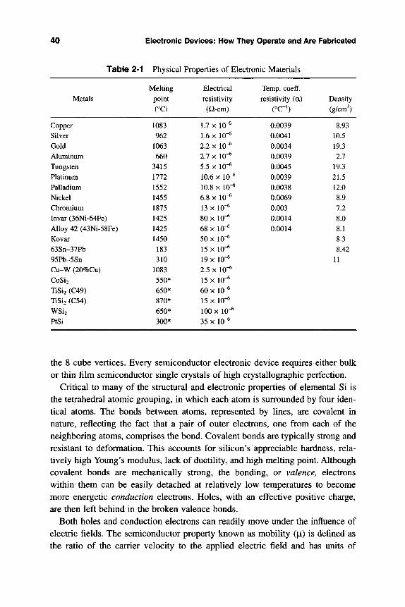
40 Electronic Devices: How They Operate and Are Fabricated
Table 2-1 Physical Properties of Electronic Materials
Metals
Copper Silver Gold Aluminum Tungsten Platinum Palladium Nickel Chromium Invar (36Ni-64Fe) Alloy 42 (43Ni-58Fe) Kovar 63Sn-37Pb 95Pb-5Sn Cu-W (20%Cu)
CoSij TiSi2 (C49) TiSiz (C54) WSi2 PtSi
Melting point
CQ
1083 962
1063 660
3415 1772 1552 1455 1875 1425 1425 1450
183 310
1083 550* 650* 870* 650* 300*
Electrical resistivity
(Q-cm)
1.7 X 10"^ 1.6 X 10"^ 2.2 X 10^ 2.7 X 10"^ 5.5 X 10"^ 10.6 X 10"^ 10.8 X 10"^ 6.8 X 10"^ 13 X 10"^ 80 X 10"^ 68 X 10"^ 50 X 10"^ 15 X 10"^ 19 X 10"^ 2.5 X 10"^ 15 X 10-^ 60 X 10-^ 15 X 10"^ 100 X10^ 35 X 10"^
Temp, coeff. resistivity (a)
CC-')
0.0039 0.0041 0.0034 0.0039 0.0045 0.0039 0.0038 0.0069 0.003 0.0014 0.0014
Density
(g/cm')
8.93 10.5 19.3 2.7
19.3 21.5 12.0 8.9 7.2 8.0 8.1 8.3 8.42
11
the 8 cube vertices. Every semiconductor electronic device requires either bulk or thin film semiconductor single crystals of high crystallographic perfection.
Critical to many of the structural and electronic properties of elemental Si is the tetrahedral atomic grouping, in which each atom is surrounded by four iden-tical atoms. The bonds between atoms, represented by lines, are covalent in nature, reflecting the fact that a pair of outer electrons, one from each of the neighboring atoms, comprises the bond. Covalent bonds are typically strong and resistant to deformation. This accounts for silicon's appreciable hardness, rela-tively high Young's modulus, lack of ductility, and high melting point. Although covalent bonds are mechanically strong, the bonding, or valence, electrons within them can be easily detached at relatively low temperatures to become more energetic conduction electrons. Holes, with an effective positive charge, are then left behind in the broken valence bonds.
Both holes and conduction electrons can readily move under the influence of electric fields. The semiconductor property known as mobility (|i) is defined as the ratio of the carrier velocity to the applied electric field and has units of
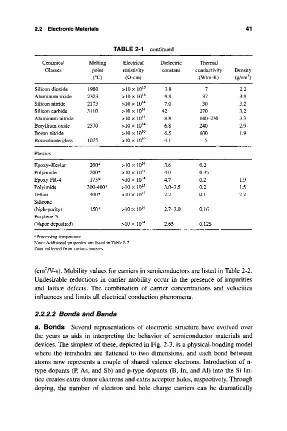
2.2 Electronic Materials 41
TABLE 2-1 eontinued
Ceramics/ Glasses
Silicon dioxide Aluminum oxide Silicon nitride Silicon carbide Aluminum nitride Beryllium oxide Boron nitride Borosilicate glass
Melting point (^C)
1980 2323 2173 3110
2570
1075
Electrical resistivity
(Q-cm)
>10 X 10 ^ >10 X 10^ >10 X 10^^ >10 X 10^^ >10 X 10 ^ >10 X 10^^ >10x 10^^ >10 X 10^^
Dielectric constant
3.8 9.9 7.0
42 8.8 6.8 6.5 4.1
Thermal conductivity
(W/m-K)
7 37 30
270 140-230 240 600
5
Density (g/cm')
2.2 3.9 3.2 3.2 3.3 2.9 1.9
Plastics
Epoxy-Kevlar Polyimide Epoxy FR-4 Polyimide Teflon Silicone (high-purity) Parylene N (Vapor deposited)
200* 200* 175*
300-400* 400*
150*
>10 X 10^^ >10x 10^^ >10x 10^^ >10 X 10 ^ >10 X 10^^
>10 X 10^^
>10 X 10^^
3.6 4.0 4,7 3.0-3.5 2.2
2.7-3.0
2.65
0.2 0.35 0.2 0.2 0.1
0.16
0.12S
1.9 1.5 2.2
•Processing temperature Note: Additional properties are listed in Table 8-2. Data collected from various sources.
(cm A^-s). Mobility values for carriers in semiconductors are listed in Table 2-2. Undesirable reductions in carrier mobility occur in the presence of impurities and lattice defects. The combination of carrier concentrations and velocities influences and limits all electrical conduction phenomena.
2.2.2.2 Bonds and Bands
a. Bonds Several representations of electronic structure have evolved over the years as aids in interpreting the behavior of semiconductor materials and devices. The simplest of these, depicted in Fig. 2-3, is a physical-bonding model where the tetrahedra are flattened to two dimensions, and each bond between atoms now represents a couple of shared valence electrons. Introduction of n-type dopants (P, As, and Sb) and p-type dopants (B, In, and Al) into the Si lat-tice creates extra donor electrons and extra acceptor holes, respectively. Through doping, the number of electron and hole charge carriers can be dramatically
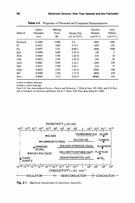
42 Electronic Devices: How They Operate and Are Fabricated
Material
Diamond Si Ge ZnS ZnSe CdS AlAs GaP GaAs InP InAs
Table 2-2 Properties of Elemental and Compound
Lattice Parameter
(nm)
0.3560 0.5431 0.5657 0.5409 0.5669 0.5832 0.5661 0.5451 0.5653 0.5869 0.6068
Melting Point
(K)
-4300 1685 1231 3200 1790 1750 1870 1750 1510 1338 1215
Energy Gap (eV at 25°C)
5.4 1.121 0.68 1 3.54 D 2.58 D 2.42 D 2.161 2.261 1.43 D 1.27 D 0.36 D
Semiconductors
Electron Mobility (cmW-s)
1800 1450 3600
120 530 340
1200 110
8500 4600
30000
Hole Mobility (cm^A -s)
1400 450
1900 5
28 50
420 75
400 150 460
I refers to indirect band gap. D refers to direct band gap. From S.M. Sze, Semiconductor Devices—Physics and Technology, J. Wiley & Sons. NY (1985), and B. R. Pam-plin in Handbook of Chemistry and Physics, Ed. R. C. Weast, CRC Press, Boca Raton FL (1980).
RESISTIVITY p (a -cm)
10^8 10^6 10^4 10^2 1010 108 106 10^ 102 1 10-2 lO"^ 10"^ 10-8 I ' I '—r~^—r^—r^—r^
GERMANIUM (Ge) SILVER I ' I ' I " \ r
• GLASS
•ALUMINUM NITRIDE SILICON (Si)
^ DIAMOND (PURE)
•EPOXY,POLYMIDE
1 FUSED QUARTZ
COPPER
GALLIUM ARSENIDE (GaAs) ALUMINUM
GALLIUM PHOSPHIDE (GaP) PLATINUM
INDIUM PHOSPHIDE (InP) •TiSio
I I I L_^ L_L. I I I L I • I I • I _L I I 10-18 10-16 10-14 10-12 10-10 10-8 10-8 10-4 10-2 1 102 10^ 10^ ^0^
CONDUCTIVITY a (H-cm)-''
INSULATOR 4 SEMICONDUCTOR - k CONDUCTOR -
Fig. 2-1 Electrical resistivities of electronic materials.
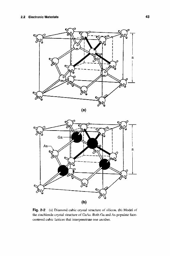
2.2 Electronic Materials 43
Fig. 2-2 (a) Diamond cubic crystal structure of silicon, (b) Model of the zincblende crystal structure of GaAs. Both Ga and As populate face-centered cubic lattices that interpenetrate one another.
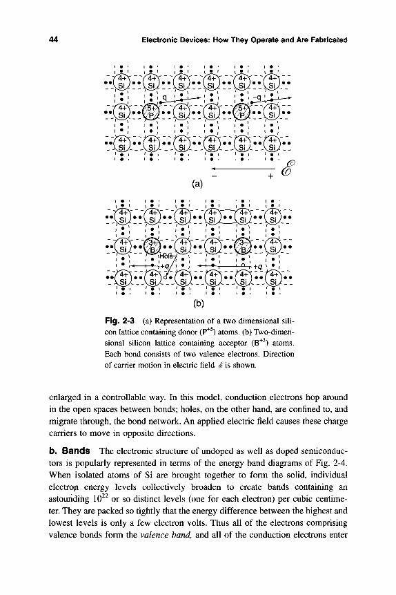
44 Electronic Devices: i-iow They Operate and Are Fabricated
® 4-K\ /4+\ f4+\ SI/. _ \S\J- - -vSu
4+N
(f
^4+N
(a)
• ' I • ' I • ' I •
' T l ' * ! I * ! I * ! I * ! I * !
"IS "Hole-
!!VsiJ!!\
. \ S t l . A S i / . . -\3>J- - -VSL/- - - V S L / - -
(b)
Fig. 2-3 (a) Representation of a two dimensional sili-con lattice containing donor (P" ) atoms, (b) Two-dimen-sional silicon lattice containing acceptor (B" ) atoms. Each bond consists of two valence electrons. Direction of carrier motion in electric field (f is shown.
enlarged in a controllable way. In this model, conduction electrons hop around in the open spaces between bonds; holes, on the other hand, are confined to, and migrate through, the bond network. An applied electric field causes these charge carriers to move in opposite directions.
b. Bands The electronic structure of undoped as well as doped semiconduc-tors is popularly represented in terms of the energy band diagrams of Fig. 2-4. When isolated atoms of Si are brought together to form the solid, individual electroji energy levels collectively broaden to create bands containing an astounding 10^^ or so distinct levels (one for each electron) per cubic centime-ter. They are packed so tightly that the energy difference between the highest and lowest levels is only a few electron volts. Thus all of the electrons comprising valence bonds form the valence band, and all of the conduction electrons enter
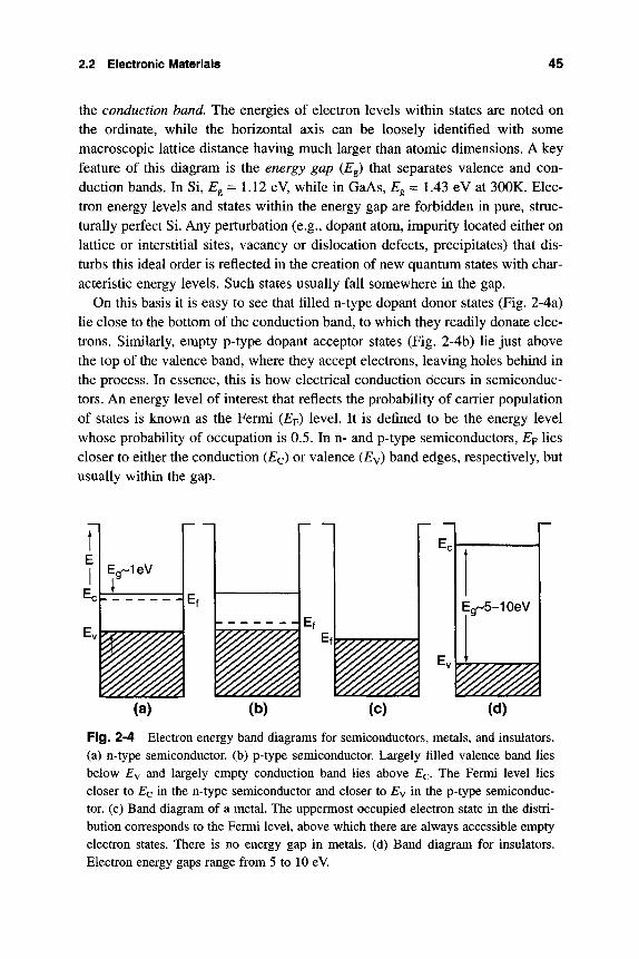
2.2 Electronic Materials 45
the conduction band. The energies of electron levels within states are noted on the ordinate, while the horizontal axis can be loosely identified with some macroscopic lattice distance having much larger than atomic dimensions. A key feature of this diagram is the energy gap (Eg) that separates valence and con-duction bands. In Si, £g = 1.12 eV, while in GaAs, Eg = 1.43 eV at 300K. Elec-tron energy levels and states within the energy gap are forbidden in pure, struc-turally perfect Si. Any perturbation (e.g., dopant atom, impurity located either on lattice or interstitial sites, vacancy or dislocation defects, precipitates) that dis-turbs this ideal order is reflected in the creation of new quantum states with char-acteristic energy levels. Such states usually fall somewhere in the gap.
On this basis it is easy to see that filled n-type dopant donor states (Fig. 2-4a) he close to the bottom of the conduction band, to which they readily donate elec-trons. Similarly, empty p-type dopant acceptor states (Fig. 2-4b) lie just above the top of the valence band, where they accept electrons, leaving holes behind in the process. In essence, this is how electrical conduction occurs in semiconduc-tors. An energy level of interest that reflects the probability of carrier population of states is known as the Fermi (Ep) level. It is defined to be the energy level whose probability of occupation is 0.5. In n- and p-type semiconductors, Ep lies closer to either the conduction (EQ) or valence (Ey) band edges, respectively, but usually within the gap.
Fig. 2-4 Electron energy band diagrams for semiconductors, metals, and insulators, (a) n-type semiconductor, (b) p-type semiconductor. Largely filled valence band lies below Ey and largely empty conduction band lies above EQ. The Fermi level lies closer to EQ in the n-type semiconductor and closer to Ey in the p-type semiconduc-tor, (c) Band diagram of a metal. The uppermost occupied electron state in the distri-bution corresponds to the Fermi level, above which there are always accessible empty electron states. There is no energy gap in metals, (d) Band diagram for insulators. Electron energy gaps range from 5 to 10 eV.
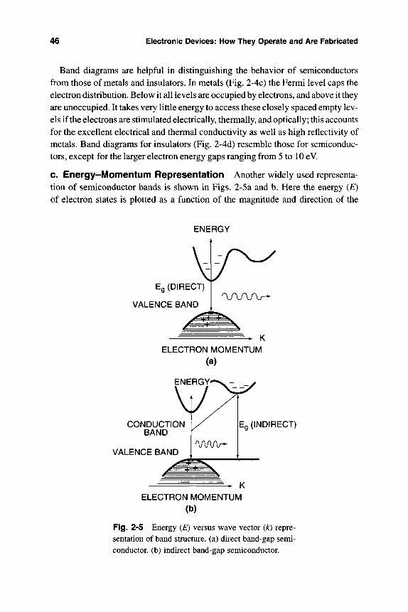
46 Electronic Devices: How Tliey Operate and Are Fabricated
Band diagrams are helpful in distinguishing the behavior of semiconductors from those of metals and insulators. In metals (Fig. 2-4c) the Fermi level caps the electron distribution. Below it all levels are occupied by electrons, and above it they are unoccupied. It takes very little energy to access these closely spaced empty lev-els if the electrons are stimulated electrically, thermally, and optically; this accounts for the excellent electrical and thermal conductivity as well as high reflectivity of metals. Band diagrams for insulators (Fig. 2-4d) resemble those for semiconduc-tors, except for the larger electron energy gaps ranging from 5 to 10 eV.
c. Energy-Momentum Representation Another widely used representa-tion of semiconductor bands is shown in Figs. 2-5a and b. Here the energy (E) of electron states is plotted as a function of the magnitude and direction of the
ENERGY
Eg (DIRECT)
VALENCE BAND O A A A / -
K ELECTRON MOMENTUM
(a)
ENERGY'
CONDUCTION BAND
Eg (INDIRECT)
VALENCE BAND
ELECTRON MOMENTUM (b)
Fig. 2-5 Energy (E) versus wave vector (k) repre-sentation of band structure, (a) direct band-gap semi-conductor, (b) indirect band-gap semiconductor.
2.2 Electronic Materials 47
electron momentum, or equivalently, versus wave vector (k). The resultant parabola-like E vs k curve is important because it provides a useful way to dis-tinguish between Si or Ge on the one hand, and GaAs as well as similar com-pound semiconductors on the other (1). While the former are known as indirect band-gap semiconductors, the latter are direct band-gap semiconductors. Only direct-gap semiconductors are useful in optical devices like light-emitting diodes (LED) or lasers. Photons of the band-gap energy are emitted when electrons descend from the bottom of the conduction band to recombine with holes at the top of the valence band. The transition between the two involved states must conserve electron momentum. Similarly, when a photon whose energy is equal to or greater than the gap energy is absorbed, momentum conservation governs the electron ascent between the corresponding valence and conduction band states. In direct band-gap materials like GaAs and InP these electron descents and ascents are vertical, conserving momentum; but in Si and other indirect semiconductors the transitions are "slanted" and involve momentum changes that effectively excite lattice vibrations which heat the solid. These wasteful processes dramatically reduce the probability that photons will either be emitted or absorbed during respective electron-hole recombination or generation.
2.2.2.3 Compound Semiconductors The important III-V compound semiconductors are derived from atomic combinations arising from columns III A (e.g., Al, Ga, In) and V A (e.g., N, P, As) of the periodic table. Other II-VI compound semiconductors are composed of elements from columns II B (Zn, Cd, Hg) and VIA (S, Se, Te). A sunmiary of the electrical properties of elemen-tal and compound semiconductors is reproduced in Table 2-2, where lattice para-meters, energy gaps, and mobilities are indicated for the more widely used mate-rials. Ternary (3 atom) and quaternary (4 atom) semiconductors are also widely used in electro-optical applications. For example, AlGaAs ternaries are derived from AlAs and GaAs mixtures. Similarly, InGaAs and GalnAsP devices used in optical communications can be understood as combinations of binary com-pounds, e.g., GaAs and InAs, and GaAs and InP. In many instances the resultant ternary energy gap and lattice parameter values are simply weighted averages derived from the constituent binaries. Thus by alloying GaAs and GaP, families of light-emitting diodes with compositions GaAsj.^P^ become available, pro-vided that the ternary semiconductor alloys are still direct-gap materials. For x = 0.4, interpolation yields an energy gap of ~ 1.9 eV, which from Eq. 2-1 below corresponds to the red portion of the spectrum.
When films of Al ^Gai. ^As deposited on GaAs substrates, or InGaAs deposited on InP, are involved, it is essential that the film be epitaxial. This means that film and substrate must be "lattice matched" or have as nearly identical lattice para-
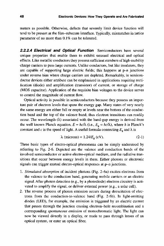
48 Electronic Devices: How They Operate and Are Fabricated
meters as possible. Otherwise, defects that severely limit device function will tend to be present at the film-substrate interface. Typically, mismatches in lattice parameter of no more than 0.1% can be tolerated.
2.2,2.4 Electrical and Optical Function Semiconductors have several unique properties that enable them to exhibit unusual electrical and optical effects. Like metallic conductors they possess sufficient numbers of high-mobility charge carriers to pass large currents. Unlike conductors, but like insulators, they are capable of supporting large electric fields; this happens at p-n junctions under reverse bias where charge carriers are depleted. Remarkably, in semicon-ductor devices either attribute can be emphasized in applications requiring recti-fication (diode) and amplification (transistor) of current, or storage of charge (MOS capacitor). Application of the requisite bias voltages to the device serves to control the magnitude of current flow.
Optical activity is possible in semiconductors because they possess an impor-tant pair of electron levels that spans the energy gap. Many states of very nearly the same energy are either full or empty at levels near the bottom of the conduc-tion band and the top of the valence band; thus electron transitions can readily occur. The wavelength QC) associated with the band-gap energy is derived from the well known Planck equation, E = hc/X (i.e., £g = hc/X), where h is Planck's constant and c is the speed of light. A useful formula connecting Eg and X is
X (microns) = 1.24/£g (eV). (2-1)
Three basic types of electro-optical phenomena can be simply understood by referring to Fig. 2-6. Depicted are the valence and conduction bands of the involved semiconductor or active electro-optical medium, and the radiative tran-sitions that occur between energy levels in them. Either photons or electronic signals can trigger mutual electro-optical responses at p-n junctions.
1. Stimulated absorption of incident photons (Fig. 2-6a) excites electrons from the valence to the conduction band, generating mobile carriers or an electric signal. After photon detection (e.g., by a photodiode) electron circuitry is acti-vated to amplify the signal, or deliver external power (e.g., a solar cell).
2. The reverse process of photon emission occurs during deexcitation of elec-trons from the conduction-to-valence band (Fig. 2-6b). In light-emitting diodes (LED), for example, the emission is triggered by an electric current that passes through the junction causing electron-hole recombination and a corresponding spontaneous emission of monochromatic light. The light can now be viewed directly in a display, or made to pass through lenses of an optical system, or enter an optical fiber.
2.2 Electronic Materials 49
EPITAXIAL LAYERS
I I p-lnP • InGaAsP I n-lnP
I I 1 I
ENERGY E L E C T R O N ^ ' (CURRENT)
n f I CONDUCTION I / I £ _ J BAND him^^\
h v > E ,
~ \ mm hv
hv
_^i_'"-L^i_ _^i_
hv
HOLE
THICKNESS
IPHOTODIODE I
STIMULATED ABSORPTION
(a)
I LIGHT-EMITTING D I O D J I
SPONTANEOUS EMISSION
(b)
LASER
STIMULATED EMISSION
(C)
Fig. 2-6 Basic electron transitions between valence and conduction bands in semiconduc-tors shown within the context of junction devices, (a) Stimulated absorption, (b) Spontaneous emission, (c) Stimulated emission.
3. The last case (Fig. 2-6c) combines features of the previous two. Through absorption of light (pumping), electrons ascend from the valence band to an excited state, causing a normally unnatural, inverted population of electron levels. Incident photons that impinge on such excited atoms may now induce stimulated emission of photons from them. These photons have the same energy and phase as those that excited them in the first place. If instead of allowing the light to exit the medium it is made to reflect back and forth in phase, while impinging on other atoms in excited states, the light intensity is amplified. This is the basis of laser action.
Just how the electro-optical effects are capitalized upon in actual devices is addressed later in the chapter.
2.2.3 Conductors
Conductors are used in circuits to speed the transmission of electronic signals from where they are generated to where they are processed, e.g., detected, ampli-fied, stored, or displayed, without distortion or any loss of information. In solid-state circuits this means that conductors must first make low-resistance contact
50 Electronic Devices: How They Operate and Are Fabricated
to various n and p doped regions, and gate electrodes of devices, and then be connected to other active devices and passive components via a network of inter-connections. The latter are found in great profusion on the IC chip itself as well as at the (packaging) interface between the chip and the outside world. Degra-dation of both contacts and interconnections may alter the fidelity of the intended signal by changing its amplitude, time constant, sign, and shape; fre-quently, open circuiting is the final manifestation of conductor degradation.
Properties required of conductors include high electrical conductivity (to min-imize both Joule heating and RC time constants), chemical stability (absence of corrosion), ability to be easily processed into required shapes with desired dimensions, compatibility with other device processing and fabrication steps, and lastly, resistance to loss of dimensional and physical integrity due to stress or the passage of large current densities (electromigration). Because the conduc-tivity requirement is often the critical one, conductors are limited to metals. These materials have face-centered and body-centered cubic crystal structures for the most part. Unlike semiconductors, in all practical applications metals are poly crystalline. Relevant properties of metals are given in Table 2-1.
Of the 80 or so metallic elements only a few (e.g., Al, Cu, Au, Ag ) have seen extensive use in commercial electronic devices and systems. On IC chips, inter-connections are basically limited to Al and Al alloy (Al-Cu, Al-Cu-Si) metal-lizations at any given level, and to W/TiN via combinations to connect levels. But, when contacts to semiconductors and external connectors are considered, a much richer assortment of metals, alloys (Ti-W, PdSi, Sn-Pb solder), and inter-metallic compounds (TiSi2) is utilized. Metal contacts and interconnections at several levels within ICs are schematically indicated in Fig. 2-7 together with typical sites and types of degradation.
Metals are good conductors of electricity because they contain huge numbers of free or conduction electrons; i.e., Cu has 1 and Al has 3 per atom, so we are dealing with -lO^^per cm^. Their band structures are complex, but importantly, metals possess either overlapping valence and conduction bands or an unfilled conduction band. Further, the absence of energy gaps means that electrons never face any appreciable barrier in accessing the numerous, closely spaced, empty higher energy states under the stimulus of an applied electric field or incident photon. Two simple relationships govern the resistivity, p, of metals:
PXotal = PT + Pi + Pd (2-2)
and
p = P o ( l + a A r ) . (2-3)
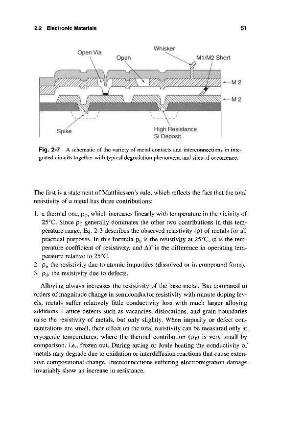
2.2 Electronic Materials 51
Open Via Whisker
M1/M2 Short
-M2
M2
High Resistance Si Deposit
Fig. 2-7 A schematic of the variety of metal contacts and interconnections in inte-grated circuits together with typical degradation phenomena and sites of occurrence.
The first is a statement of Matthiessen's rule, which reflects the fact that the total resistivity of a metal has three contributions:
1. a thermal one, pT, which increases linearly with temperature in the vicinity of 25°C. Since px generally dominates the other two contributions in this tem-perature range, Eq. 2-3 describes the observed resistivity (p) of metals for all practical purposes. In this formula po is the resistivity at 25°C, a is the tem-perature coefficient of resistivity, and AT is the difference in operating tem-perature relative to 25°C.
2. pi, the resistivity due to atomic impurities (dissolved or in compound form). 3. pd, the resistivity due to defects.
Alloying always increases the resistivity of the base metal. But compared to orders of magnitude change in semiconductor resistivity with minute doping lev-els, metals suffer relatively little conductivity loss with much larger alloying additions. Lattice defects such as vacancies, dislocations, and grain boundaries raise the resistivity of metals, but only slightly. When impurity or defect con-centrations are small, their effect on the total resistivity can be measured only at cryogenic temperatures, where the thermal contribution (px) is very small by comparison, i.e., frozen out. During arcing or Joule heating the conductivity of metals may degrade due to oxidation or interdiffusion reactions that cause exten-sive compositional change. Interconnections suffering electromigration damage invariably show an increase in resistance.
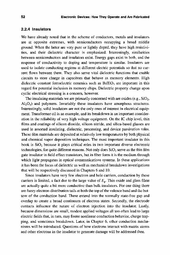
52 Electronic Devices: How They Operate and Are Fabricated
2.2.4 Insulators
We have already noted that in the scheme of conductors, metals and insulators are at opposite extremes, with semiconductors occupying a broad middle ground. When the latter are very pure or lightly doped, they have high resistivi-ties, and their dielectric character is emphasized. Interestingly, similarities between semiconductors and insulators exist. Energy gaps exist in both, and the response of conductivity to doping and temperature is similar. Insulators are used to isolate conducting regions at different electric potentials so that no cur-rent flows between them. They also serve vital dielectric functions that enable circuits to store charge in capacitors that behave as memory elements. High dielectric constant ferroelectric ceramics such as BaTiOa are important in this regard for potential inclusion in memory chips. Dielectric property change upon cyclic electrical stressing is a concern, however.
The insulating materials we are primarily concerned with are oxides (e.g., Si02, AI2O3) and polymers. Invariably these insulators have amorphous structures. Interestingly, solid insulators are not the only ones of interest in electrical equip-ment. Transformer oil is an example, and its breakdown is an important consider-ation in the reliability of very high voltage equipment. On the IC chip level, thin films and coatings of silicon dioxide, silicon nitride, and silica-based glasses are used in assorted insulating, dielectric, processing, and device passivation roles. These film materials are deposited at relatively low temperatures by both physical and chemical vapor deposition techniques. The most important insulator in this book is Si02 because it plays critical roles in two important diverse electronic technologies, for quite different reasons. Not only does Si02 serve as the thin film gate insulator in field effect transistors, but in fiber form it is the medium through which light propagates in optical communications systems. In these applications it has been the focus of dielectric as well as mechanical breakdown investigations that will be respectively discussed in Chapters 6 and 10.
Since insulators have very few electron and hole carriers, conduction by these carriers is limited, a fact due to the large value of E^. Thin oxide and glass films are actually quite a bit more conductive than bulk insulators. For one thing there are fuzzy electron-distribution tails at both the top of the valence band and the bot-tom of the conduction band. These extend into the normally state-free gap and overlap to create a broad continuum of electron states. Secondly, the electrode contacts influence the nature of electron injection into the insulator. Lastly, because dimensions are small, modest applied voltages all too often lead to large electric fields that, in turn, may foster nonlinear conduction behavior, charge trap-ping, and sometimes breakdown. Later, in Chapter 6, other conduction mecha-nisms will be introduced. Questions of how electrons interact with matrix atoms and other electrons in the insulator to generate damage will be addressed then.
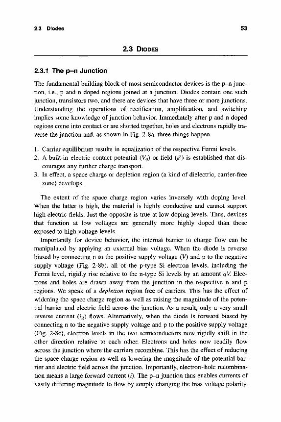
2.3 Diodes 53
2.3 DIODES
2.3.1 The p-n Junction
The fundamental building block of most semiconductor devices is the p-n junc-tion, i.e., p and n doped regions joined at a junction. Diodes contain one such junction, transistors two, and there are devices that have three or more junctions. Understanding the operations of rectification, amplification, and switching implies some knowledge of junction behavior. Immediately after p and n doped regions come into contact or are shorted together, holes and electrons rapidly tra-verse the junction and, as shown in Fig. 2-8a, three things happen.
1. Carrier equilibrium results in equalization of the respective Fermi levels. 2. A built-in electric contact potential (VQ) or field ((f) is established that dis-
courages any further charge transport. 3. In effect, a space charge or depletion region (a kind of dielectric, carrier-free
zone) develops.
The extent of the space charge region varies inversely with doping level. When the latter is high, the material is highly conductive and cannot support high electric fields. Just the opposite is true at low doping levels. Thus, devices that function at low voltages are generally more highly doped than those exposed to high voltage levels.
Importantly for device behavior, the internal barrier to charge flow can be manipulated by applying an external bias voltage. When the diode is reverse biased by connecting n to the positive supply voltage (V) and p to the negative supply voltage (Fig. 2-8b), all of the p-type Si electron levels, including the Fermi level, rigidly rise relative to the n-type Si levels by an amount qV Elec-trons and holes are drawn away from the junction in the respective n and p regions. We speak of a depletion region free of carriers. This has the effect of widening the space charge region as well as raising the magnitude of the poten-tial barrier and electric field across the junction. As a result, only a very small reverse current (/R) flows. Alternatively, when the diode is forward biased by connecting n to the negative supply voltage and p to the positive supply voltage (Fig. 2-8c), electron levels in the two semiconductors now rigidly shift in the other direction relative to each other. Electrons and holes now readily flow across the junction where the carriers recombine. This has the effect of reducing the space charge region as well as lowering the magnitude of the potential bar-rier and electric field across the junction. Importantly, electron-hole recombina-tion means a large forward current (/). The p-n junction thus enables currents of vastly differing magnitude to flow by simply changing the bias voltage polarity.
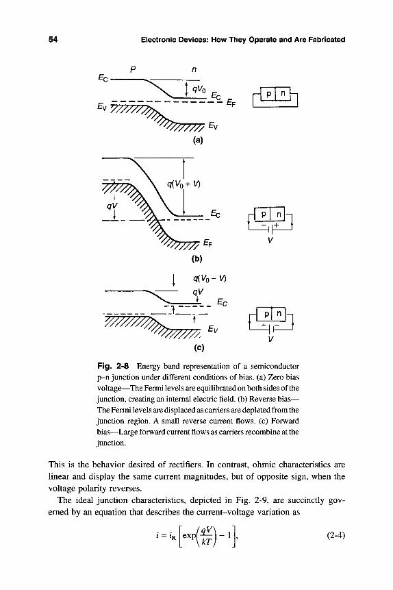
54 Electronic Devices: IHow Tliey Operate and Are Fabricated
t QVO
^777777, [ 1 ^ ^
V777^^^ (a)
nh
(c)
f l / Q^a
Fig. 2-8 Energy band representation of a semiconductor p-n junction under different conditions of bias, (a) Zero bias voltage—The Fermi levels are equilibrated on both sides of the junction, creating an internal electric field, (b) Reverse bias— The Fermi levels are displaced as carriers are depleted from the junction region. A small reverse current flows, (c) Forward bias—Large forward current flows as carriers recombine at the junction.
This is the behavior desired of rectifiers. In contrast, ohmic characteristics are linear and display the same current magnitudes, but of opposite sign, when the voltage polarity reverses.
The ideal junction characteristics, depicted in Fig. 2-9, are succinctly gov-erned by an equation that describes the current-voltage variation as
1 = 1^ expi ^ \ _ i kT
(2-4)
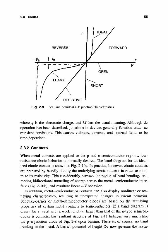
2.3 Diodes 55
RESISTIVE
Fig. 2-9 Ideal and nonideal /-V junction characteristics.
where q is the electronic charge, and kT has the usual meaning. Although dc operation has been described, junctions in devices generally function under ac transient conditions. This causes voltages, currents, and internal fields to be time-dependent.
2.3.2 Contacts
When metal contacts are applied to the p and n semiconductor regions, low-resistance ohmic behavior is normally desired. The band diagram for an ideal-ized ohmic contact is shown in Fig. 2-lOa. In practice, however, ohmic contacts are prepared by heavily doping the underlying semiconductor in order to mini-mize its resistivity. This considerably narrows the region of band bending, pro-moting bidirectional tunneling of charge across the metal-semiconductor inter-face (Fig. 2-10b), and resultant linear /-V behavior.
In addition, metal-semiconductor contacts can also display nonlinear or rec-tifying characteristics, resulting in unexpected changes in circuit behavior. Schottky-barrier or metal-semiconductor diodes are based on the rectifying properties of certain metal contacts to semiconductors. If a band diagram is drawn for a metal with a work function larger than that of the n-type semicon-ductor it contacts; the resultant structure of Fig. 2-11 behaves very much like the p-n junction diode of Fig. 2-8 upon biasing. There is, of course, no band bending in the metal. A barrier potential of height OB now governs the asym-
56 Electronic Devices: How They Operate and Are Fabricated
q^s
\ _
y///////////M
(a)
t I
V////////////A - • & -Ec
(b)
Fig. 2-10 (a) Band diagram representation for an idealized ohmic contact between a metal and semiconductor, (b) Band diagram for an ohmic contact illustrating tunneling. OM and Os are respective work functions.
metric transport of charge across the junction. Despite the fact that the i-V characteristics appear identical, Schottky-barrier and p-n diodes differ in one significant way. Under forward bias, majority electrons injected over the barrier are hotter than normal electrons in the metal. Their excess energy is very rapidly quenched, and such thermalized electrons cannot flow back into the semiconductor upon reverse bias because they face a large energy barrier in that direction. The short recovery time of 10" ^ seconds makes Schottky diodes capable of very fast switching in microwave circuits.
Applications normally require either ohmic or Schottky behavior; interest-ingly, certain compound-semiconductor field-effect transistors contain both
2.3 Diodes 57
t
W//////////A
q^s
Fig. 2-11 Band diagram for idealized Schottky-barrier contact between a metal and semiconductor.
ohmic and Schottky contacts (Sect. 2.7.4). Irrespective of whether they are ohmic or rectifying, solid-state reactions between Al contacts and silicon as well as assorted metals (e.g., Au, Ti) and GaAs have been troublesome sources of degradation and failure in devices. These reliability problems are exacerbated when high current densities flow through contacts.
2.3.3 Deviations from Ideal Junction Behavior
There are a number ways that actual junction behavior differs from the ideal.
2,3.3.1 Characteristics. Rather than by Eq. 2-4, diode i-V characteristics
are more nearly described by / = /R [exp n kT
-1] , where n, the ideality factor.
varies between 1 and 2. In addition, the contact potential due to work function dif-ferences between the involved semiconductors makes the i-V forward character-istics appear to be more squarish. Thus, very little forward current flows until a critical voltage somewhat below E^ is applied, after which the current rises very steeply.
Several effects serve to weaken rectifying behavior, resulting in the deviations from good i-V characteristics displayed in Fig. 2-9. Ohmic losses in diodes are manifested by passage of less current at high forward bias levels. Carrier genera-tion outside of the junction region means higher reverse currents. These effects cause the diode to be more resistive and display linear /-V behavior as a limiting
58 Electronic Devices: How Tliey Operate and Are Fabricated
case. In poorly made diodes the reverse current may sometimes have a surface component that leaks around the junction. Charged contaminants and semicon-ductor surface states foster electrical leakage paths. The proportions of bulk and surface currents depend on the electrical character of the junction at the point where the bulk meets the surface. Passivating Si diodes with Si02 layers mini-mizes such leakage. In good diodes the reverse current remains very small and then sharply increases at the point of breakdown, a subject discussed in the next section. Such characteristics are "hard," distinguishing them from the "softer" i-V behavior exhibited by junctions possessing weak spots where localized break-downs cause excessive leakage current.
Finally, there are the characteristics of the open diode that passes no current irrespective of voltage, and the shorted diode through which large currents flow at zero voltage.
2.3.3.2 Breakdown Diode breakdown is much less alarming than it sounds and does not necessarily mean damage. When the applied reverse voltage is increased beyond certain limits (Fig. 2-9) diodes undergo breakdown. Depend-ing on doping level, electric fields in the junction ranging from 200 to 1000 kV/cm can develop in Si. Under such conditions minority carriers that produce the usual reverse or leakage current are accelerated to kinetic energies high enough for them to ionize matrix atoms upon collisional impact. In the case of a single incident electron, two electrons (the original one and the impacted valence electron) will now reside in the conduction band after collision. Each can impact-ionize lattice atoms repeatedly, and with sufficient electron multiplica-tion, avalanche breakdown may occur. The reverse current rises to a value lim-ited only by the external resistance of the circuit. In this state it may operate sat-isfactorily as a reverse-biased diode. However, if the reverse current is excessive, the junction can overheat, causing the diode to bum out. Zener diodes capitalize on operation in the breakdown state and are used as voltage references in rectifier and control circuits.
2.3.3.3 Punch-through Although the term sounds as ominous as break-down, punch-through is not necessarily threatening to continued diode function. Punch-through occurs when lightly doped regions are also physically thin. Upon reverse biasing, the depletion region widens and may extend directly to the ohmic contact, thus shorting out the diode or transistor. Provided that the current flow is limited by the circuit resistance and no overheating occurs, the diode will recover its former properties when the reverse voltage is reduced. As we shall see later, punch-through also occurs in transistors.
2.4 Bipolar Transistors 59
2.4 BIPOLAR TRANSISTORS
2.4.1 Transistors in General
Transistors are the most important solid state devices. Because they are also the most numerous, device reliability and failure issues tend to be overwhelmingly focused on them. Since transistors contain two p-n junctions, have three con-tacts or terminals, are complex geometrically, and frequently require the action of perpendicular electrical fields, their behavior is more difficult to understand than that of diodes. To complicate matters further there are two fundamentally different types; in the bipolar junction transistor (BJT) current is amplified, while in the field effect transistor (FET) a voltage controls a current. The former rely on the participation of both types of carriers, hence the descriptor "bipolar." In contrast, only one carrier plays a prominent role in FETs. Transistors perform the basic electrical functions of amplification and switching in both discrete and IC configurations involving low as well as large power applications.
With regard to function it is helpful to distinguish between linear and on-off digital logic circuits. Linear circuits typically operate with low input voltage lev-els of perhaps ~l|iV or so (e.g., audio equipment) and outputs having small deviations about a quiescent operating dc level. Digital circuits are constrained to operate at fixed voltage levels (e.g., 0 or 5 V) and are impervious to noise lev-els that would present difficulty in linear circuitry. The latter are much less tol-erant of variations in electrical component characteristics than is the case for digital circuits. With change in operating temperature, linear circuits may drift in and out of specifications, whereas digital circuits will either function properly or abruptly fail. Both BJTs and FETs are used in linear and digital circuits; com-puter logic and memory circuits are primarily composed of FETs, however, and these therefore dominate the transistor market.
2.4.2 Bipolar Junction Transistors
2,4.2.1 Operation It is conmion to start discussions of BJTs with the p-n-p type shown in Fig. 2-12 because the direction of majority carrier (hole) motion coin-cides with that of the current flow. There is also an n-p-n version of this device that is easier to fabricate. Since the electron mobility in Si (jig = 1450 cmW-s) is some three times higher than for holes, these faster n-p-n devices are preferred in most applications. By reversing the doping type, bias voltages, and current direction, the treatment applies to n-p-n devices as well. These three-terminal devices con-tain two junctions separating three semiconducting regions, i.e., the emitter, base, and collector. In the case under discussion these are doped p, n, and p, respec-
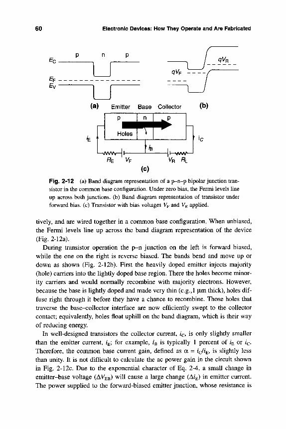
60 Electronic Devices: How They Operate and Are Fabricated
Esj
I QVB
qVp
(a)
'E •
Emitter Base Collector
P ^ ^ ^ ^ P ^
Holes 1 ^ 1
''B 1, r VWv
(b)
'c
RE Vp VR f?L
(c) Fig. 2-12 (a) Band diagram representation of a p-n-p bipolar junction tran-sistor in the common base configuration. Under zero bias, the Fermi levels Une up across both junctions, (b) Band diagram representation of transistor under forward bias, (c) Transistor with bias voltages Vp and VR applied.
tively, and are wired together in a common base configuration. When unbiased, the Fermi levels line up across the band diagram representation of the device (Fig. 2-12a).
During transistor operation the p-n junction on the left is forward biased, while the one on the right is reverse biased. The bands bend and move up or down as shown (Fig. 2-12b). First the heavily doped emitter injects majority (hole) carriers into the lightly doped base region. There the holes become minor-ity carriers and would normally recombine with majority electrons. However, because the base is lightly doped and made very thin (e.g.,1 |Lim thick), holes dif-fuse right through it before they have a chance to recombine. Those holes that traverse the base-collector interface are now efficiently swept to the collector contact; equivalently, holes float uphill on the band diagram, which is their way of reducing energy.
In well-designed transistors the collector current, ic, is only slightly smaller than the emitter current, i^; for example, i^ is typically 1 percent of i^ or /c-Therefore, the common base current gain, defined as a = ic/iE^ is slightly less than unity. It is not difficult to calculate the ac power gain in the circuit shown in Fig. 2-12c. Due to the exponential character of Eq. 2-4, a small change in emitter-base voltage (AVEB) will cause a large change (A/g) in emitter current. The power supplied to the forward-biased emitter junction, whose resistance is
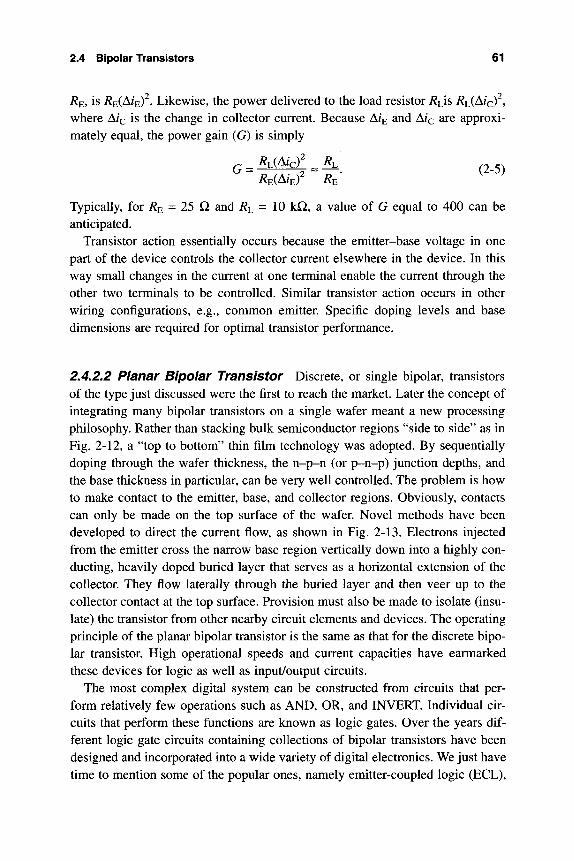
2.4 Bipolar Transistors 61
/?E, is /?E(A^E)^- Likewise, the power delivered to the load resistor Ri}s Ri^(Aicf, where AIQ is the change in collector current. Because A/g and A/c are approxi-mately equal, the power gain (G) is simply
^^M^^K (2-5)
Typically, for R^ = 25 Q. and Rj^ = 10 kQ, a value of G equal to 400 can be anticipated.
Transistor action essentially occurs because the emitter-base voltage in one part of the device controls the collector current elsewhere in the device. In this way small changes in the current at one terminal enable the current through the other two terminals to be controlled. Similar transistor action occurs in other wiring configurations, e.g., common emitter. Specific doping levels and base dimensions are required for optimal transistor performance.
2.4.2.2 Planar Bipolar Transistor Discrete, or single bipolar, transistors of the type just discussed were the first to reach the market. Later the concept of integrating many bipolar transistors on a single wafer meant a new processing philosophy. Rather than stacking bulk semiconductor regions "side to side" as in Fig. 2-12, a "top to bottom" thin film technology was adopted. By sequentially doping through the wafer thickness, the n-p-n (or p-n-p) junction depths, and the base thickness in particular, can be very well controlled. The problem is how to make contact to the emitter, base, and collector regions. Obviously, contacts can only be made on the top surface of the wafer. Novel methods have been developed to direct the current flow, as shown in Fig. 2-13. Electrons injected from the emitter cross the narrow base region vertically down into a highly con-ducting, heavily doped buried layer that serves as a horizontal extension of the collector. They flow laterally through the buried layer and then veer up to the collector contact at the top surface. Provision must also be made to isolate (insu-late) the transistor from other nearby circuit elements and devices. The operating principle of the planar bipolar transistor is the same as that for the discrete bipo-lar transistor. High operational speeds and current capacities have earmarked these devices for logic as well as input/output circuits.
The most complex digital system can be constructed from circuits that per-form relatively few operations such as AND, OR, and INVERT. Individual cir-cuits that perform these functions are known as logic gates. Over the years dif-ferent logic gate circuits containing collections of bipolar transistors have been designed and incorporated into a wide variety of digital electronics. We just have time to mention some of the popular ones, namely emitter-coupled logic (ECL),
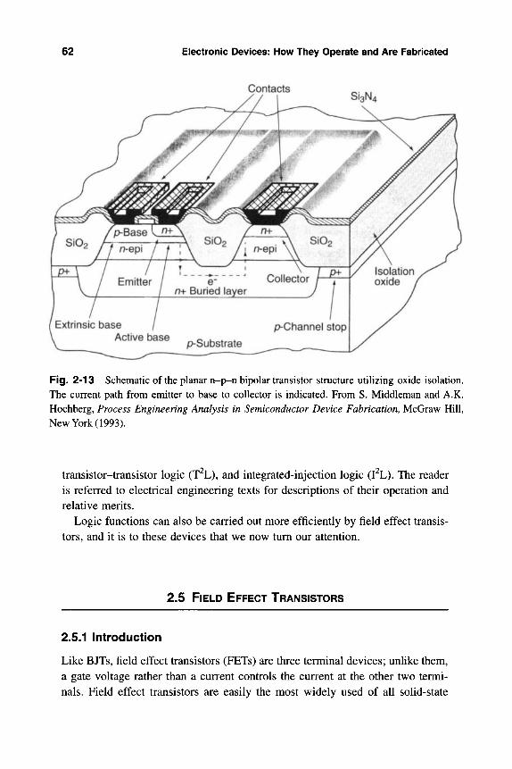
62 Electronic Devices: How They Operate and Are Fabricated
Contacts
Fig. 2-13 Schematic of the planar n-p-n bipolar transistor structure utilizing oxide isolation. The current path from emitter to base to collector is indicated. From S. Middleman and A.K. Hochberg, Process Engineering Analysis in Semiconductor Device Fabrication, McGraw Hill, New York (1993).
transistor-transistor logic (T^L), and integrated-injection logic (I^L). The reader is referred to electrical engineering texts for descriptions of their operation and relative merits.
Logic functions can also be carried out more efficiently by field effect transis-tors, and it is to these devices that we now turn our attention.
2.5 FIELD EFFECT TRANSISTORS
2.5.1 Introduction
Like BJTs, field effect transistors (FETs) are three terminal devices; unlike them, a gate voltage rather than a current controls the current at the other two termi-nals. Field effect transistors are easily the most widely used of all solid-state
2.5 Field Effect Transistors 63
devices. They currently dominate computer logic as well as memory integrated circuit chips and are projected to widen this dominance. At the outset, two dis-tinct types of field effect transistor must be distinguished. The first and most important is the metal oxide semiconductor (MOS) type, where the metal (M) gate electrode is separated from the semiconductor (S) by a thin insulator film (i.e., Si02). Voltage applied to the gate controls the current flow between under-lying semiconductor regions by either creating or eliminating a conducting chan-nel. Junction field effect transistors (JFET) are the second type, and they func-tion by applying a gate voltage to vary the depletion width of a reverse-biased p-n junction.
2.5.2 The MOS Capacitor
Knowing how the MOS capacitor structure responds to applied voltage is pre-requisite to understanding MOS field effect transistor (MOSFET) behavior. This capacitor structure, which is the essential building block of silicon MOSFETs as well as charge coupled devices, actually consists of two capacitors in series. The first has a fixed value of capacitance determined by the thin Si02 film sand-wiched between planar metal (or other conductor, e.g., polysilicon or silicide) and semiconductor electrodes. Underlying this is the capacitance associated with Si, which varies depending on the extent of charge depletion in the semiconduc-tor. Now consider the "ideal" MOS structure for p-type Si, shown in Fig. 2-14a. With no gate voltage or bias applied, Fermi level equilibration leaves all bands horizontal, or flat; this condition arises because the work functions of the metal and semiconductor are the same, and there is no oxide charge. When a negative gate voltage (-VG) is applied to the metal, the energy of all of its conduction electrons is raised uniformly by an amount qV relative to Si. Holes are attracted to the Si/Si02 interface, making Si there appear to be even more p-type than originally. This causes band bending at the interface (Fig. 2-14b), which graphi-cally describes a state known as accumulation. The high interfacial hole density effectively serves to make the Si a positively conducting capacitor plate. For high -VG values, the MOS capacitance (Co), which depends inversely on Si02 thickness, is large and solely due to the oxide.
As the polarity of VG is reversed, the overall capacitance decreases. The rea-son is that holes are repelled from the Si/Si02 interface. In this depletion regime Si acts like a dielectric with a capacitance governed by the width of the deple-tion region (Fig. 2-14c). The two series capacitors have a lower overall capaci-tance than that of either the semiconductor or oxide alone. Now the bands bend the other way; the slope of the oxide conduction band edge or electric field reverses sign, and near the interface the semiconductor acquires an n-like char-
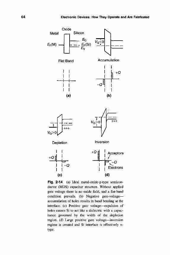
64 Electronic Devices: How They Operate and Are Fabricated
Oxide Metal .—. Silicon N
EF(M)
Flat Band N
Accumulation
I I
+0
-Q i
(a) (b)
Inversion
+Q -tr
-Q
(c)
+Q Acceptors
Electrons
(d)
Fig. 2-14 (a) Ideal metal-oxide-p-type semicon-ductor (MOS) capacitor structure. Without applied gate voltage there is no oxide field, and a flat-band condition prevails, (b) Negative gate-voltage— accumulation of holes results in band bending at the interface, (c) Positive gate voltage—expulsion of holes causes Si to act like a dielectric with a capac-itance governed by the width of the depletion region, (d) Large positive gate voltage—inversion regime is created and Si interface is effectively n-type.
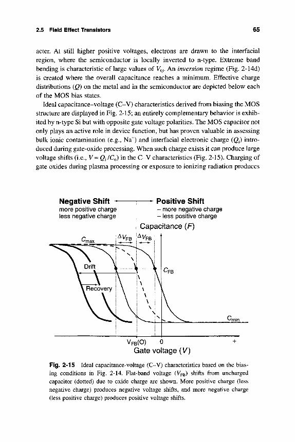
2.5 Field Effect Transistors 65
acter. At still higher positive voltages, electrons are drawn to the interfacial region, where the semiconductor is locally inverted to n-type. Extreme band bending is characteristic of large values of VG- An inversion regime (Fig. 2-14d) is created where the overall capacitance reaches a minimum. Effective charge distributions (Q) on the metal and in the semiconductor are depicted below each of the MOS bias states.
Ideal capacitance-voltage (C-V) characteristics derived from biasing the MOS structure are displayed in Fig. 2-15; an entirely complementary behavior is exhib-ited by n-type Si but with opposite gate voltage polarities. The MOS capacitor not only plays an active role in device function, but has proven valuable in assessing bulk ionic contamination (e.g., Na" ) and interfacial electronic charge (Qi) intro-duced during gate-oxide processing. When such charge exists it can produce large voltage shifts (i.e., V=Qi /Co) in the C-V characteristics (Fig. 2-15). Charging of gate oxides during plasma processing or exposure to ionizing radiation produces
Negative Shift -^ more positive charge less negative charge
Positive Shift - more negative charge - less positive charge
Capacitance (F) i^VpB 'M
VFB(O) 0 +
Gate voltage {V)
Fig. 2-15 Ideal capacitance-voltage (C-V) characteristics based on the bias-ing conditions in Fig. 2-14. Flat-band voltage (VFB) shifts from uncharged capacitor (dotted) due to oxide charge are shown. More positive charge (less negative charge) produces negative voltage shifts, and more negative charge (less positive charge) produces positive voltage shifts.
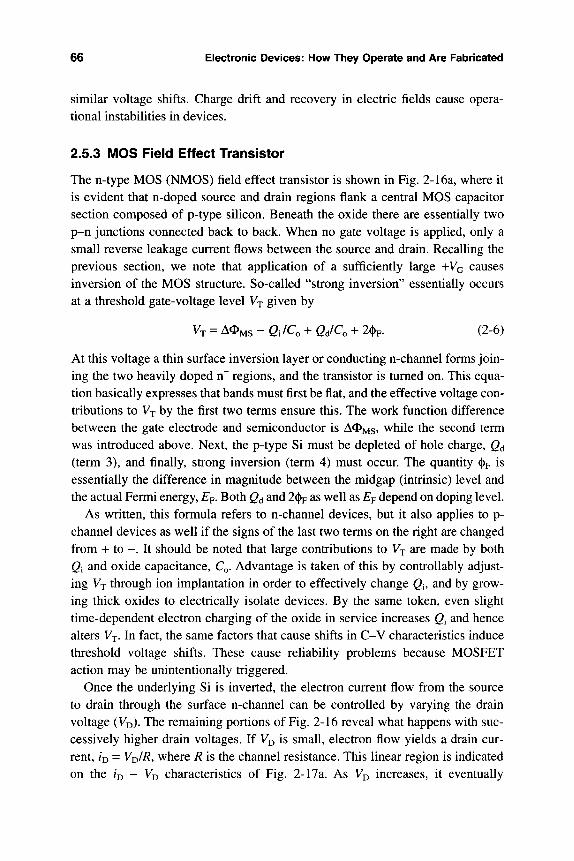
66 Electronic Devices: How They Operate and Are Fabricated
similar voltage shifts. Charge drift and recovery in electric fields cause opera-tional instabilities in devices.
2.5.3 MOS Field Effect Transistor
The n-type MOS (NMOS) field effect transistor is shown in Fig. 2-16a, where it is evident that n-doped source and drain regions flank a central MOS capacitor section composed of p-type silicon. Beneath the oxide there are essentially two p-n junctions connected back to back. When no gate voltage is applied, only a small reverse leakage current flows between the source and drain. Recalling the previous section, we note that application of a sufficiently large H-VG causes inversion of the MOS structure. So-called "strong inversion" essentially occurs at a threshold gate-voltage level Vj given by
Vj = AOMS - a /Co + Gd/Co + 2^p. (2-6)
At this voltage a thin surface inversion layer or conducting n-channel forms join-ing the two heavily doped n" regions, and the transistor is turned on. This equa-tion basically expresses that bands must first be flat, and the effective voltage con-tributions to Vj by the first two terms ensure this. The work function difference between the gate electrode and semiconductor is AOMS» while the second term was introduced above. Next, the p-type Si must be depleted of hole charge, Qd (term 3), and finally, strong inversion (term 4) must occur. The quantity (J)F is essentially the difference in magnitude between the midgap (intrinsic) level and the actual Fermi energy, Ep. Both gd ^^^ '^^F as well as Ep depend on doping level.
As written, this formula refers to n-channel devices, but it also applies to p-channel devices as well if the signs of the last two terms on the right are changed from -H to - . It should be noted that large contributions to Vj are made by both Qi and oxide capacitance, Q . Advantage is taken of this by controllably adjust-ing VT through ion implantation in order to effectively change Qi, and by grow-ing thick oxides to electrically isolate devices. By the same token, even slight time-dependent electron charging of the oxide in service increases Q^ and hence alters VT- In fact, the same factors that cause shifts in C-V characteristics induce threshold voltage shifts. These cause reliability problems because MOSFET action may be unintentionally triggered.
Once the underlying Si is inverted, the electron current flow from the source to drain through the surface n-channel can be controlled by varying the drain voltage (VD)- The remaining portions of Fig. 2-16 reveal what happens with suc-cessively higher drain voltages. If V^ is small, electron flow yields a drain cur-rent, /D = Vj)/R, where R is the channel resistance. This linear region is indicated on the ij) - V^ characteristics of Fig. 2-17a. As VD increases, it eventually
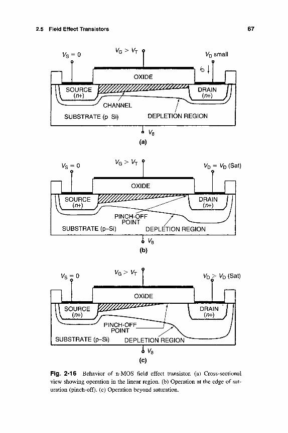
2.5 Field Effect Transistors 67
Us = 0 VQ>VT
I VQ small
OXIDE io\
SOURCE ^ ^ ^ ^ ^ ^ ^ DRAIN 711 "7
CHANNEL
SUBSTRATE (p-Si) DEPLETION REGION
A Va
(a)
V/Q > VT ? VD = VD (Sat)
Q
^s = 0 VD > VD (Sat) o
POINT
SUBSTRATE (p-SI) DEPLETION REGION^
TVo (c)
Fig. 2-16 Behavior of n-MOS field effect transistor, (a) Cross-sectional view showing operation in the linear region, (b) Operation at the edge of sat-uration (pinch-off), (c) Operation beyond saturation.
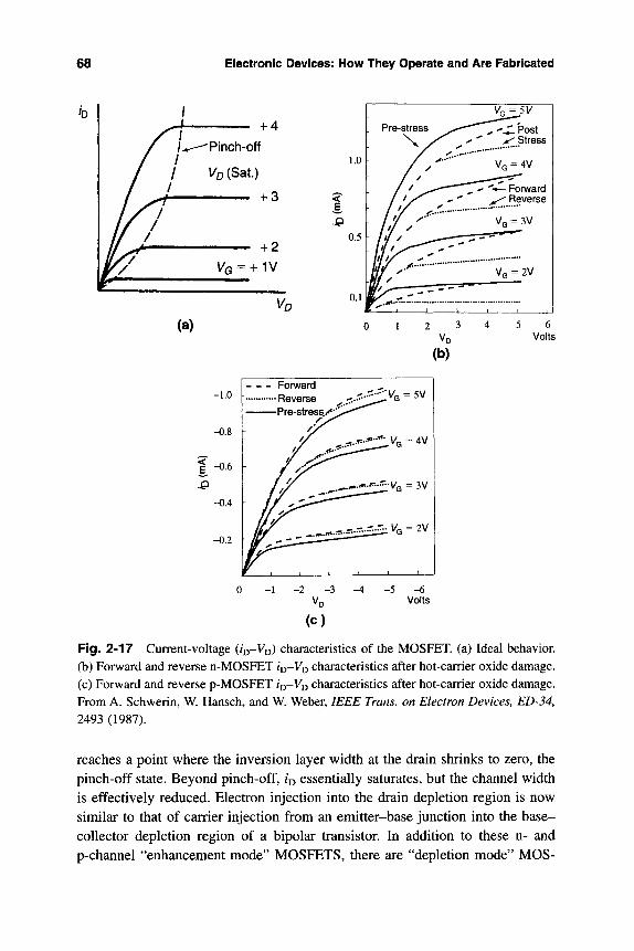
68 Electronic Devices: How They Operate and Are Fabricated
1.0
0.5
0.1
y ^ y
Pre-stress ^ " ^ ^ ^ *post \ ^ y^ • ^ ^ Stress
/ ^ ^ • • " " " VQ = 4V
/ / ^ — • ^^^'V-Forward / f / ^ ^ ^ ^ Reverse
W, "'"' VG = 2V
mt^^ * » ' * ' *
r-';" ;• T" r : , 0 1 3 4 5 6
Volts
(b)
Forward Reverse Pre-stress./*'^
. .--•:i' G = 5v
Fig. 2-17 Current-voltage (/D-V^D) characteristics of the MOSFET. (a) Ideal behavior. (b) Forward and reverse n-MOSFET /D-VD characteristics after hot-carrier oxide damage. (c) Forward and reverse p-MOSFET /Q-VD characteristics after hot-carrier oxide damage. From A. Schwerin, W. Hansch, and W. Weber, IEEE Trans, on Electron Devices, ED-34, 2493 (1987).
reaches a point where the inversion layer width at the drain shrinks to zero, the pinch-off state. Beyond pinch-off, i^ essentially saturates, but the channel width is effectively reduced. Electron injection into the drain depletion region is now similar to that of carrier injection from an emitter-base junction into the base-collector depletion region of a bipolar transistor. In addition to these n- and p-channel "enhancement mode" MOSFETS, there are "depletion mode" MOS-
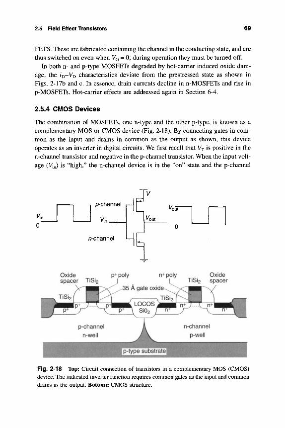
2.5 Field Effect Transistors 69
FETS. These are fabricated containing the channel in the conducting state, and are thus switched on even when VQ = 0; during operation they must be turned off.
In both n- and p-type MOSFETs degraded by hot-carrier induced oxide dam-age, the IU-VD characteristics deviate from the prestressed state as shown in Figs. 2-17b and c. In essence, drain currents decline in n-MOSFETs and rise in p-MOSFETs. Hot-carrier effects are addressed again in Section 6-4.
2.5.4 CMOS Devices
The combination of MOSFETs, one n-type and the other p-type, is known as a complementary MOS or CMOS device (Fig. 2-18). By connecting gates in com-mon as the input and drains in common as the output as shown, this device operates as an inverter in digital circuits. We first recall that VT is positive in the n-channel transistor and negative in the p-channel transistor. When the input volt-age (^in) is "high," the n-channel device is in the "on" state and the p-channel
p-channel
n-channel
out
^ouT
0
Oxide spacer TiSi2
p+ poly n+ poly
5 A gate oxide TiSi
Oxide spacer
p-type substrate
n-channel p-well
Fig. 2-18 Top: Circuit connection of transistors in a complementary MOS (CMOS) device. The indicated inverter function requires common gates as the input and common drains as the output. Bottom: CMOS structure.
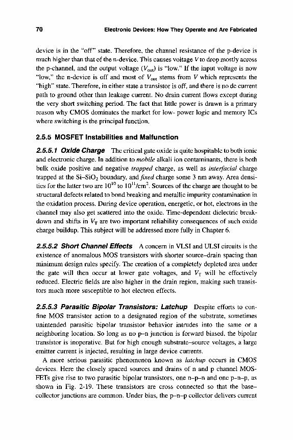
70 Electronic Devices: How They Operate and Are Fabricated
device is in the "off" state. Therefore, the channel resistance of the p-device is much higher than that of the n-device. This causes voltage V to drop mostly across the p-channel, and the output voltage (Vout) is "low." If the input voltage is now "low," the n-device is off and most of Vout stems from V which represents the "high" state. Therefore, in either state a transistor is off, and there is no dc current path to ground other than leakage current. No drain current flows except during the very short switching period. The fact that little power is drawn is a primary reason why CMOS dominates the market for low- power logic and memory ICs where switching is the principal function.
2.5.5 MOSFET Instabilities and Malfunction
2.5.5.1 Oxide Charge The critical gate oxide is quite hospitable to both ionic and electronic charge. In addition to mobile alkali ion contaminants, there is both bulk oxide positive and negative trapped charge, as well as interfacial charge trapped at the Si-Si02 boundary, dind fixed charge some 3 nm away. Area densi-ties for the latter two are 10^^ to lO^Vcm . Sources of the charge are thought to be structural defects related to bond breaking and metallic impurity contamination in the oxidation process. During device operation, energetic, or hot, electrons in the channel may also get scattered into the oxide. Time-dependent dielectric break-down and shifts in Vj are two important reliability consequences of such oxide charge buildup. This subject will be addressed more fully in Chapter 6.
2.5.5.2 Short Channel Effects A concern in VLSI and ULSI circuits is the existence of anomalous MOS transistors with shorter source-drain spacing than minimum design rules specify. The creation of a completely depleted area under the gate will then occur at lower gate voltages, and VT will be effectively reduced. Electric fields are also higher in the drain region, making such transis-tors much more susceptible to hot electron effects.
2.5.5.3 Parasitic Bipolar Transistors: Latchup Despite efforts to con-fine MOS transistor action to a designated region of the substrate, sometimes unintended parasitic bipolar transistor behavior intrudes into the same or a neighboring location. So long as no p-n junction is forward biased, the bipolar transistor is inoperative. But for high enough substrate-source voltages, a large emitter current is injected, resulting in large device currents.
A more serious parasitic phenomenon known as latchup occurs in CMOS devices. Here the closely spaced sources and drains of n and p channel MOS-FETs give rise to two parasitic bipolar transistors, one n-p-n and one p-n-p, as shown in Fig. 2-19. These transistors are cross connected so that the base-collector junctions are common. Under bias, the p-n-p collector delivers current
2.5 Field Effect Transistors 71
' DD
Fig. 2-19 Latchup arising in CMOS devices due the creation of closely spaced and coupled n-p-n and p-n-p parasitic bipolar transistors.
to the n-p-n base, and the n-p-n collector delivers power to the p-n-p base. If the gains of these transistors are high, both are driven into saturation, and the power supply voltages become connected through a low resistance path. In essence, a device known as a thyristor, which contains p-n-p-n doped regions, is effectively created. Carriers generated in unwanted regions by leakage cur-rents, substrate current, or even photon irradiation can trigger latchup. When this happens, short-circuit currents rapidly overheat the IC chip, destroying it. Better design of transistor isolation is effective in combating latchup.
2.5.6 Bipolar versus CMOS
Now that the two major transistor technologies have been introduced, it is peda-gogically worthwhile to compare the characteristics and attributes of each type of device (11).
a. Size. Using the same lithography tools, the footprint of bipolar transistors is typically 20-40 percent larger than the corresponding MOS transistor. A key advantage of CMOS technology is the smaller device area, which translates to a higher packing density.
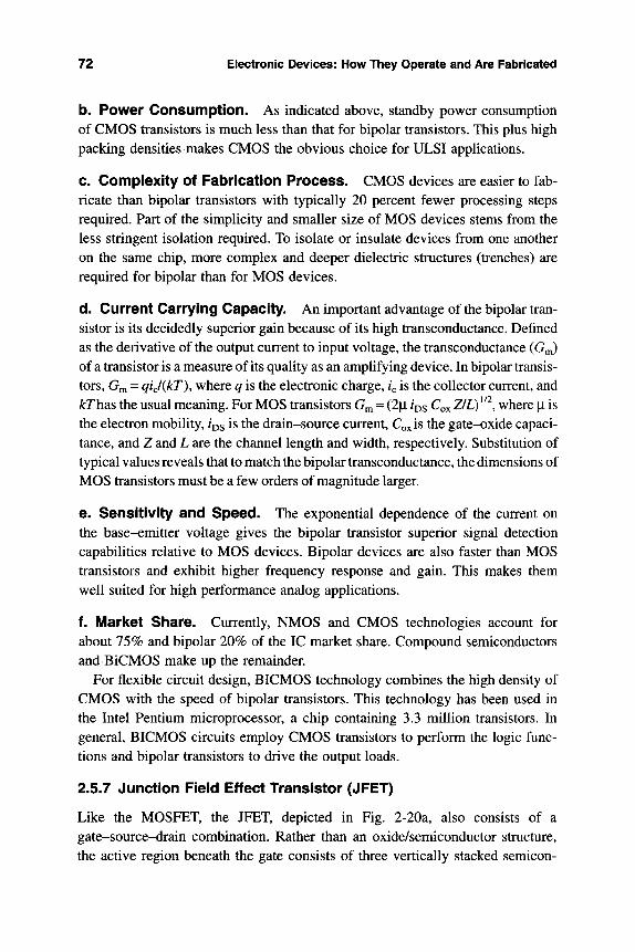
72 Electronic Devices: How They Operate and Are Fabricated
b. Power Consumption. As indicated above, standby power consumption of CMOS transistors is much less than that for bipolar transistors. This plus high packing densities makes CMOS the obvious choice for ULSI applications.
c. Complexity of Fabrication Process. CMOS devices are easier to fab-ricate than bipolar transistors with typically 20 percent fewer processing steps required. Part of the simplicity and smaller size of MOS devices stems from the less stringent isolation required. To isolate or insulate devices from one another on the same chip, more complex and deeper dielectric structures (trenches) are required for bipolar than for MOS devices.
d. Current Carrying Capacity. An important advantage of the bipolar tran-sistor is its decidedly superior gain because of its high transconductance. Defined as the derivative of the output current to input voltage, the transconductance (Gm) of a transistor is a measure of its quality as an amplifying device. In bipolar transis-tors, Gm = qiJikT), where q is the electronic charge, i^ is the collector current, and kThsiS the usual meaning. For MOS transistors G^ = (2|i /DS QX ZILf'^, where |i is the electron mobility, /QS is the drain-source current, Qxis the gate-oxide capaci-tance, and Z and L are the channel length and width, respectively. Substitution of typical values reveals that to match the bipolar transconductance, the dimensions of MOS transistors must be a few orders of magnitude larger.
e. Sensitivity and Speed. The exponential dependence of the current on the base-emitter voltage gives the bipolar transistor superior signal detection capabilities relative to MOS devices. Bipolar devices are also faster than MOS transistors and exhibit higher frequency response and gain. This makes them well suited for high performance analog applications.
f. lUarlcet SKiare. Currently, NMOS and CMOS technologies account for about 75% and bipolar 20% of the IC market share. Compound semiconductors andBiCMOS make up the remainder.
For flexible circuit design, BICMOS technology combines the high density of CMOS with the speed of bipolar transistors. This technology has been used in the Intel Pentium microprocessor, a chip containing 3.3 million transistors. In general, BICMOS circuits employ CMOS transistors to perform the logic func-tions and bipolar transistors to drive the output loads.
2.5.7 Junction Field Effect Transistor (JFET)
Like the MOSFET, the JFET, depicted in Fig. 2-20a, also consists of a gate-source-drain combination. Rather than an oxide/semiconductor structure, the active region beneath the gate consists of three vertically stacked semicon-
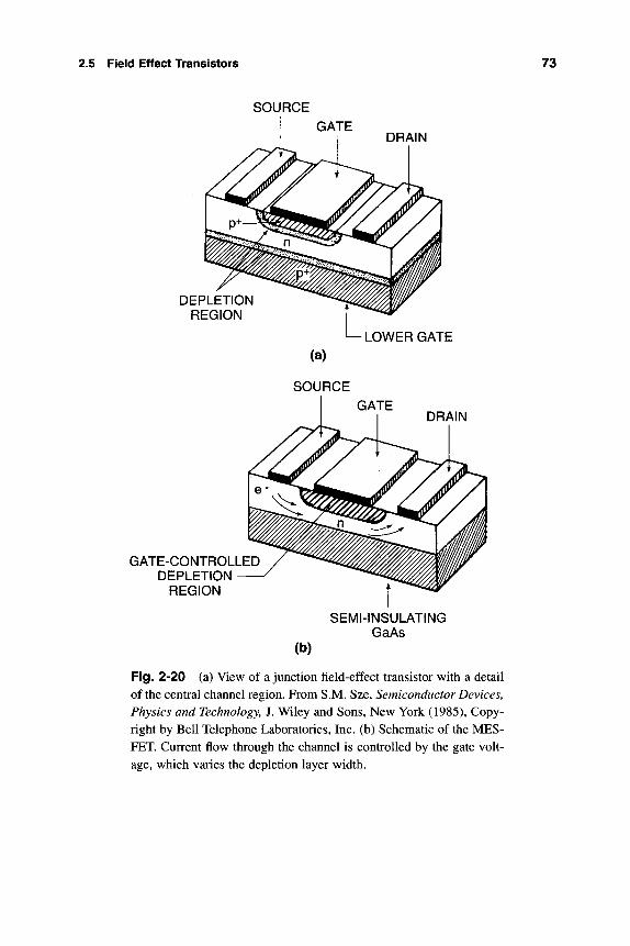
2.5 Field Effect Transistors 73
SOURCE
DRAIN
DEPLETION REGION
GATE-CONTROLLED DEPLETION
REGION
SEMI-INSULATING GaAs
(b)
Fig. 2-20 (a) View of a junction field-effect transistor with a detail of the central channel region. From S.M. Sze, Semiconductor Devices, Physics and Technology, J. Wiley and Sons, New York (1985), Copy-right by Bell Telephone Laboratories, Inc. (b) Schematic of the MES-FET. Current flow through the channel is controlled by the gate volt-age, which varies the depletion layer width.
74 Electronic Devices: How They Operate and Are Fabricated
ductor layers. In operation the upper and lower gates (the top and bottom heav-ily doped p-layers) are connected together, while the the lightly doped n-channel in between has the drain voltage (VD) applied across it. Both p-n junctions are slightly reverse biased initially, so that depletion layers extend into the channel. As +VD is applied, a channel current (I'D) flows whose magnitude is simply given by Ohm's law, or VD divided by the channel resistance. At larger values of Vj^, the voltage drop (i.e., bias) that progressively rises from source to drain increases both /D and the depletion width in concert. Finally, the two depletion regions merge at the drain, and the channel pinches. At that point the current sat-urates just as it does in MOSFETs and the /D-^D characteristics resemble those displayed in Fig. 2-17a.
Similar devices known as MESFETs are widely used in high-frequency circuits. Fabricated in III-V compound semiconductors, they are discussed in Sect. 2.7.3.
2.6 MEMORIES
2.6.1 Types of Memories
Together with logic chips, memory chips are critical for computer circuit appli-cations. Memories are circuits that enable the storage of digital information, or data, in terms of bits (binary digits). They now account for close to 40% of the integrated circuit market and can stand alone on a single IC chip or be embed-ded within a larger IC. A road map through the broad variety of memories used, and the categories they belong to, is shown in Fig. 2-21. Memories that lose their data when the supply voltage is removed are said to be volatile, while those that retain data under such conditions are nonvolatile. Another subdivision reveals that there are three kinds of memory—serial memory, random access memory (RAM), and read only memory (ROM). Volatile memories include serial, static (SRAM), and dynamic (DRAM) types. Three-quarters of the total memory mar-ket, including both volatile and nonvolatile, is dominated by DRAMs. In serial memories, data enters and leaves in the same sequence, so the "first in" is the "first out." Charge coupled devices (CCD) described later are used in such mem-ories for video applications.
Random access memories, which come in SRAM and DRAM varieties, are arranged in a matrix array and require both read-write data and address inputs and data outputs. Data can either be written or read directly in a random way, unlike memory locations on magnetic tape, which must be lined up with the read-write head. Storage of data occurs within memory cells. In SRAMs these cells contain
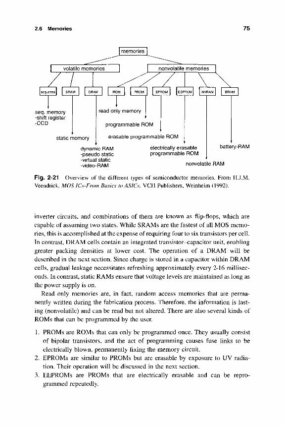
2.6 Memories 75
seq. memory -shift register -CCD
static memory
read only memory
programmable ROM
erasable programmable ROM
dynamic RAM -pseudo static -virtual static -video-RAM
electrically erasable programmable ROM
battery-RAM
nonvolatile RAM
Fig. 2-21 Overview of the different types of semiconductor memories. From HJ.M. Veendrick, MOS ICs-From Basics to ASICs, VCH Publishers, Weinheim (1992).
inverter circuits, and combinations of them are known as flip-flops, which are capable of assuming two states. While SRAMs are the fastest of all MOS memo-ries, this is accomplished at the expense of requiring four to six transistors per cell. In contrast, DRAM cells contain an integrated transistor-capacitor unit, enabling greater packing densities at lower cost. The operation of a DRAM will be described in the next section. Since charge is stored in a capacitor within DRAM cells, gradual leakage necessitates refreshing approximately every 2-16 millisec-onds. In contrast, static RAMs ensure that voltage levels are maintained as long as the power supply is on.
Read only memories are, in fact, random access memories that are perma-nently written during the fabrication process. Therefore, the information is last-ing (nonvolatile) and can be read but not altered. There are also several kinds of ROMs that can be programmed by the user.
1. PROMs are ROMs that can only be programmed once. They usually consist of bipolar transistors, and the act of programming causes fuse links to be electrically blown, permanently fixing the memory circuit.
2. EPROMs are similar to PROMs but are erasable by exposure to UV radia-tion. Their operation will be discussed in the next section.
3. EEPROMs are PROMs that are electrically erasable and can be repro-grammed repeatedly.
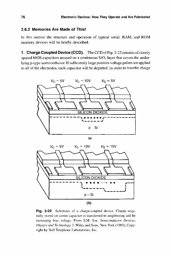
76 Electronic Devices: How They Operate and Are Fabricated
2.6.2 Memories Are Made of This!
In this section the structure and operation of typical serial, RAM, and ROM
memory devices will be briefly described.
1. Charge Coupled Device (CCD). The CCD of Fig. 2-22 consists of closely spaced MOS capacitors arrayed on a continuous Si02 layer that covers the under-
lying p-type semiconductor. If sufficiently large positive voltage pulses are applied
to all of the electrodes, each capacitor will be depleted. In order to transfer charge
Vr. = 5V Va = 10V Vc. = 5V
VQ = 5V VQ = 10V Va = 15V
Fig. 2-22 Schematic of a charge-coupled device. Charge origi-nally stored on center capacitor is transferred to neighboring cell by increasing bias voltage. From S.M. Sze, Semiconductor Devices, Physics and Technology, J. Wiley and Sons, New York (1985), Copy-right by Bell Telephone Laboratories, Inc.
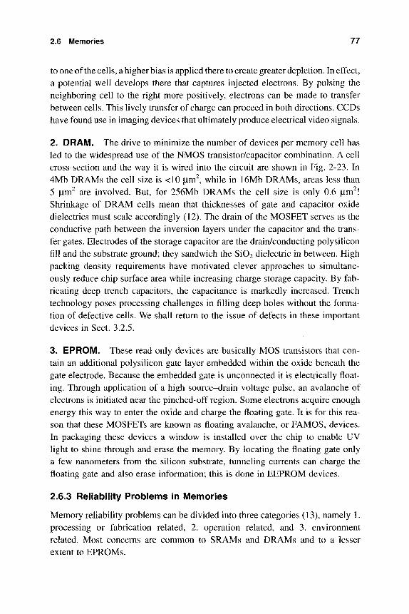
2.6 Memories 77
to one of the cells, a higher bias is applied there to create greater depletion. In effect, a potential well develops there that captures injected electrons. By pulsing the neighboring cell to the right more positively, electrons can be made to transfer between cells. This lively transfer of charge can proceed in both directions. CCDs have found use in imaging devices that ultimately produce electrical video signals.
2. DRAM. The drive to minimize the number of devices per memory cell has led to the widespread use of the NMOS transistor/capacitor combination. A cell cross-section and the way it is wired into the circuit are shown in Fig. 2-23. In 4Mb DRAMs the cell size is <10 |im^, while in 16Mb DRAMs, areas less than 5 |im^ are involved. But, for 256Mb DRAMs the cell size is only 0.6 jiim ! Shrinkage of DRAM cells mean that thicknesses of gate and capacitor oxide dielectrics must scale accordingly (12). The drain of the MOSFET serves as the conductive path between the inversion layers under the capacitor and the trans-fer gates. Electrodes of the storage capacitor are the drain/conducting poly silicon fill and the substrate ground; they sandwich the Si02 dielectric in between. High packing density requirements have motivated clever approaches to simultane-ously reduce chip surface area while increasing charge storage capacity. By fab-ricating deep trench capacitors, the capacitance is markedly increased. Trench technology poses processing challenges in filling deep holes without the forma-tion of defective cells. We shall return to the issue of defects in these important devices in Sect. 3.2.5.
3. EPROM. These read only devices are basically MOS transistors that con-tain an additional poly silicon gate layer embedded within the oxide beneath the gate electrode. Because the embedded gate is unconnected it is electrically float-ing. Through application of a high source-drain voltage pulse, an avalanche of electrons is initiated near the pinched-off region. Some electrons acquire enough energy this way to enter the oxide and charge the floating gate. It is for this rea-son that these MOSFETs are known as floating avalanche, or FAMOS, devices. In packaging these devices a window is installed over the chip to enable UV light to shine through and erase the memory. By locating the floating gate only a few nanometers from the silicon substrate, tunneling currents can charge the floating gate and also erase information; this is done in EEPROM devices.
2.6.3 Reliability Problems in Memories
Memory reliability problems can be divided into three categories (13), namely 1. processing or fabrication related, 2. operation related, and 3. environment related. Most concerns are common to SRAMs and DRAMs and to a lesser extent to EPROMs.
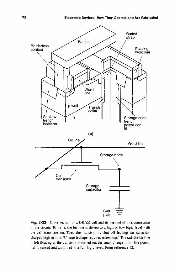
78 Electronic Devices: How They Operate and Are Fabricated
Buried strap
Borderless contact Passing
word line
Shallow-trench isolation
\ Storage node trench
icon polysili(
(a)
Word line
Storage capacitor
Cell _ plate ^
Fig. 2-23 Cross-section of a DRAM cell and its method of interconnection in the circuit. To write, the bit line is driven to a high or low logic level with the cell transistor on. Then the transistor is shut off leaving the capacitor charged high or low. (Charge leakage requires refreshing.) To read, the bit line is left floating as the transistor is turned on; the small change in bit-line poten-tial is sensed and amplified to a full logic level. From reference 12.
2.7 GaAs Devices 79
Processing difficulties include control of the conductor linewidth and semi-conductor doping levels, defects due to contamination, stress, and process-induced radiation. Yields are adversely impacted, and poor performance and degradation often show up in the infant mortality population. Adding redundant columns or rows of devices that can be programmed to substitute for failing memory cells is one of the strategies adopted to combat failed devices.
Operational reliability problems stem from the nonuniform scaling of device features to achieve high packing densities. Reduction in transistor gate lengths without corresponding changes in operating voltages has resulted in higher drain electric fields. These promote time-dependent changes in dielectric properties and threshold voltage shifts.
Environmental damage is largely related to packaging issues. On the chip level, nuclear radiation in the form of gamma rays and alpha particles, which may originate in the packaging materials (e.g., Pb-Sn solder), impinge on mem-ory cells and ionize atoms, causing local soft errors. Chapter 7 addresses such reliability issues.
2.7 G A A S DEVICES
2.7.1 Why Compound Semiconductor Devices?
Hailed as the electronic materials of the future, advances in silicon technology have perpetually consigned compound semiconductors to a second-place status. Nevertheless, there are electronic functions that are performed inefficiently or not at all by Si devices; this is the reason for our interest in III-V materials, specifically GaAs, InP, and ternary and quaternary alloys based on these materi-als. A comparison with Si indicates several important reasons for their use in devices.
1. The speed (frequency) of devices made from compound semiconductors exceeds that for Si devices simply because electron mobilities are higher. For example. Table 2-2 reveals that |Lie(GaAs) is some six times that for |ie(Si). This shortens electron transit times and enhances high-frequency operation. Very high speed microwave devices and integrated circuits require these attributes of GaAs devices.
2. The larger band gap in GaAs relative to Si means that it can withstand higher working temperatures, an attractive property in small geometry power
80 Electronic Devices: How They Operate and Are Fabricated
devices used in microwave applications. Low power devices that operate at room temperature have correspondingly low thermal generation of carriers and leakage currents, hence low noise.
3. Direct band-gap transitions in compound semiconductors make optical emis-sion and absorption processes more efficient than in Si (Sect. 2.2.2.4). This has enabled the production of efficient lasers, light emitting diodes, and pho-todetectors.
4. Optical devices can often be made to operate at specific wavelengths within a broad spectral domain. In Si, only the wavelength corresponding to the band-gap energy is easily accessible. By alloying compound semiconductors, ternary and quaternary alloys emerge with energy gaps controllably tuned to a desired operating wavelength. Optical communications technology capital-izes on this to create high-performance light sources and detectors that oper-ate at wavelengths where minimum optical losses occur.
5. A desirable attribute of GaAs is its ability to be produced in semi-insulating form with resistivities of -10^ ^-cm. Such insulating single crystals make excellent substrates for GaAs microwave devices and integrated circuits.
Advantages seldom come without drawbacks. In GaAs we are dealing with a brittle, expensive material that is not easy to process and fabricate into devices. On the other hand. Si is mechanically robust and cheap, and signifi-cantly easier to process than GaAs. Silicon can also be protected and passi-vated by an easily grown, high-quahty Si02 film, something that cannot be done in GaAs.
The subsequent discussion reflects the division of compound semiconductor devices according to microwave and opto-electronic applications. General tutor-ial reviews of the operation, reliability, and failure of compound semiconductor devices can be found in references 14, 15, and 16.
2.7.2 Microwave Applications
Microwave frequencies range between 10^ Hz (1 GHz) to 1000 GHz with respective wavelengths of 30 to 0.03 cm. Within this spectral domain are a number of communication systems applications that are important in both the mihtary and civilian sectors. Military applications include ground and airborne radar, electronic warfare including guided weapons, and satellite communica-tions; civilian applications include microwave radar (for police, small boats, intruder alarms, and door openers), direct broadcast satellites (12 GHz) and mobile (1-3 GHz band) as well as cellular (~1 GHz) communications. To make
2.7 GaAs Devices 81
these systems function, devices that generate, detect, and ampUfy microwave signals are required. Since the Hmit for silicon devices is -1.5 GHz, GaAs devices are preferred above this frequency. Microwave circuits are sometimes difficult to design because conductors such as stray solder act like antennas at these frequencies.
2.7.3 The GaAs MESFET
By replacing the upper p-n junction of a JFET (Fig. 2-20a) by a reverse-biased Schottky barrier, the MESFET emerges. The first part of the acronym for this device, which is deposited on a semi-insulating GaAs substrate, stands for (Schottky) metal (contact) epitaxial (compound) semiconductor. In the MES-FET, schematically depicted in Fig. 2-20b, source-gate-drain electrodes com-bine to control current flow through a lightly n-doped single crystal (epitaxial) film of GaAs that serves as the channel. Sandwiching the channel are the metal contacts above and the semi-insulating GaAs substrate below. Device behavior and characteristics parallel those of the Si JFET. But GaAs MESFETS differ from their lower-frequency Si cousins because the channels are thinner (~ 0.1 jxm) and gate lengths shorter (< 1 jim). For channels of length L , the device cutoff frequency is given by vj{2 K L^), where v^ is the electron saturation velocity (~2 X 10 cm/s in GaAs). Thus for a 1 |im channel length, ~ 35 GHZ opera-tion is possible.
In addition to the low-power, small-signal MESFETs used in receiver front ends and digital integrated circuits, there are power MESFET devices that oper-ate at higher voltages. These devices contain an interdigitated, or comb-like, array of contacts that encompasses a larger area with a deep active channel. The contrast in geometries and operating conditions is reflected in different failure mechanisms for low-signal relative to high-power devices.
In contrast to the Schottky gate contact, source and drain contacts in these transistors must be ohmic (e.g., Au-Ge). Accelerated high-temperature testing of these devices has revealed failures due to the degradation of the metal employed in these contacts. "Gate sinking," a common failure mechanism involving metal interdiffusion into the GaAs, is discussed further in Chapter 5. Decrease in drain current at zero gate bias, reduction in pinch-off voltage, and degradation of channel properties (e.g., increase in drain to source lesistance) ar? some of the reliability problems associated with GaAs transistors. Improvements in gate met-allizations over the past two decades have extended device lifetimes from thou-sands of hours employing Al to millions of hours with TiPtAu.
82 Electronic Devices: How They Operate and Are Fabricated
2.7.4 High Electron Mobility Transistor (HEMT)
These quantum devices operate much like MOSFETs and exhibit gains and speeds that are among the highest for any transistors (17, 18). A common figure of merit for FETs is the transconductance, and it can be increased by reducing the channel resistance through heavy doping. But this strategy degrades electron mobility because of carrier scattering by the ionized impurities. In HEMTs, the dual desiderata of high carrier concentrations and mobilities are simultaneously achieved. This is basically accomplished at the interface between n-doped AlGaAs and undoped GaAs, as indicated in Fig. 2-24a. Electrons in the conduc-tion band of the doped AlGaAs (larger energy band gap) spill over into the GaAs (smaller energy band gap), where they are now trapped in a quantum-mechanical well that is free of ionized donor scatterers. As a result of band bending at the junction, the electrons in the well are essentially confined to a thin sheet. For this reason we speak of a two-dimensional electron gas, i.e., 2-DEG. An electric field applied normal to the page will result in enhanced carrier transport in the well channel. The effect of this so-called modulation doping is magnified at low tem-peratures because thermal scattering by vibrating lattice atoms is minimized. Incorporated within the structure of the GaAs-base HEMT shown in Fig. 2-24b is such a quantum well. Today, HEMTs also known as MODFETs have been fabri-cated with gate-lengths of approximately 0.25 |xm in InP-base semiconductors. These devices demonstrably outperform GaAs MESFETs with respect to gain and low noise. Short gate-length GaAs and InGaAs MODFETs have frequency responses above 100 GHz with switching delays of ~5 picoseconds (15).
Sinking of Schottky gates and degradation of ohmic source and drain contacts are major failure mechanisms in both MESFETs and HEMTs. Electromigration, surface oxidation of GaAs, burnout, diffusion of dopants from channels, and intermetallic phase formation in Al-Au metallizations (14) are additional degra-dation mechanisms.
2.7.5 GaAs Integrated Circuits
Many of the same reasons for the integration of discreet Si devices have driven the development of both analog and digital memory and logic GaAs ICs. Except for microwave applications, these products have lagged behind their Si counterparts. In addition, there have been imperatives to fabricate monoHthic microwave (and millimeter wave) integrated circuits, or MMICs. But microwave circuits are not simply large collections of FETs; in fact, some MMICs do not contain FETs at all! In some MMICs the number of passive circuit elements (resistors, inductors, diodes, transmission lines, interdigitated and overlay capacitors) may outnumber the FETs by a factor of ten to one (19). Recently, an extensive evaluation of
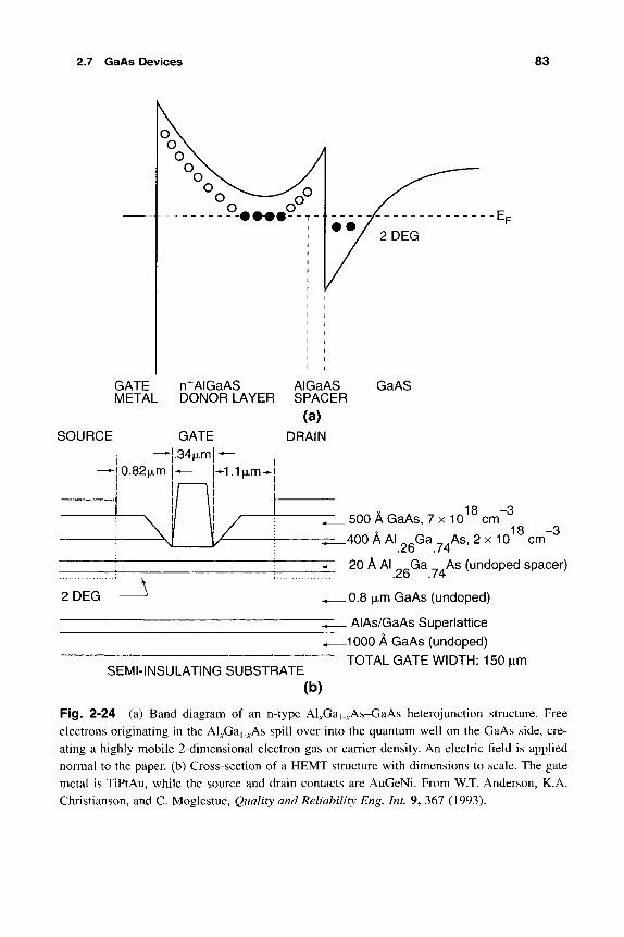
2.7 GaAs Devices 83
GATE METAL
SOURCE
i — j 0.82|jLm
1
1
n+AIGaAS DONOR LAYER
GATE | . 3 V m | ^ . 1 ^ H.1^xm-i
i n ! L If \i 1
AIGaAS SPACER
(a) DRAIN
^ \i 1/ i --^—
9 npn -
GaAS
SEMI-INSULATING SUBSTRATE
18 —3 . 500 A GaAs, 7 x 1 0 cm
_400 A Al Ga As, 2 x 1 0 ^ ^ cm~^
- 20 A Al ^^Ga _ . As (undoped spacer) .26 .74
0.8 |xm GaAs (undoped)
_ AlAs/GaAs Superlattice -1000 A GaAs (undoped) TOTAL GATE WIDTH: 150 ^m
(b)
Fig. 2-24 (a) Band diagram of an n-type Al ^Gai. ^As-GaAs heterojunction structure. Free electrons originating in the Al^Gai.^As spill over into the quantum well on the GaAs side, cre-ating a highly mobile 2-dimensional electron gas or carrier density. An electric field is applied normal to the paper, (b) Cross-section of a HEMT structure with dimensions to scale. The gate metal is TiPtAu, while the source and drain contacts are AuGeNi. From W.T. Anderson, K.A. Christianson, and C. Moglestue, Quality and Reliability Eng. Int. 9, 367 (1993).
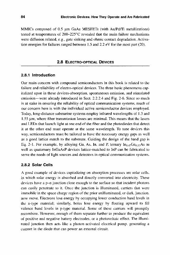
84 Electronic Devices: How Tliey Operate and Are Fabricated
MMICs composed of 0.5 |Lim GaAs MESFETs (with Au/Pd/Ti metallizations) tested at temperatures of 200-225°C revealed that the main failure mechanisms were diffusion related, e.g., gate sinking and ohmic contact degradation. Activa-tion energies for failures ranged between 1.5 and 2.2 eV for the most part (20).
2.8 ELECTRO-OPTICAL DEVICES
2.8.1 Introduction
Our main concern with compound semiconductors in this book is related to the failure and reliability of electro-optical devices. The three basic phenomena cap-italized upon in these devices-absorption, spontaneous emission, and stimulated emission—were already introduced in Sect. 2.2.2.4 and Fig. 2-6. Since so much is at stake in ensuring the reliability of optical communication systems, much of our concern here is with the individual active semiconductor devices employed. Today, long-distance submarine systems employ infrared wavelengths of 1.3 and 1.55 |im, where fiber transmission losses are minimal. This means that the lasers and LEDs that launch light at one end of the fiber and the photodiodes that detect it at the other end must operate at the same wavelength. To tune devices this way, semiconductors must be tailored to have the necessary energy gaps as well as a good lattice match to the substrate. Guiding the design of the band gap is Eq. 2-1. For example, by alloying Ga, As, In, and P, ternary IUQ 47Gao.53As as well as quaternary InGaAsP devices lattice-matched to InP can be fabricated to serve the needs of light sources and detectors in optical communication systems.
2.8.2 Solar Cells
A good example of devices capitalizing on absorption processes are solar cells, in which solar energy is absorbed and directly converted into electricity. These devices have a p-n junction close enough to the surface so that incident photons can easily penetrate to it. Once the junction is illuminated, carriers that were immobile in the space charge region of the prior unilluminated, or dark, junction, now move. Electrons lose energy by occupying lower conduction band levels in the n-type material; similarly, holes lose energy by floating upward to fill valence band levels in p-type material. Some of these carriers will promptly recombine. However, enough of them separate further to produce the equivalent of positive and negative battery electrodes, or a photovoltaic effect. The illumi-nated junction then acts like a photon-activated electrical pump, generating a current in the diode that can power an external circuit.
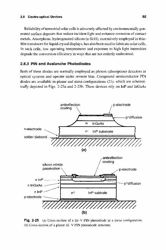
2.8 Electro-optical Devices 85
Reliability of terrestrial solar cells is adversely affected by environmentally gen-erated surface deposits that reduce incident light and enhance corrosion of contact metals. Amorphous, hydrogenated silicon (a-Si:H), extensively employed in thin-film transistors for liquid crystal displays, has also been used to fabricate solar cells. In such cells, low operating temperatures and exposure to high light intensities degrade the conversion efficiency in ways that are not entirely understood.
2.8.3 PIN and Avalanche Photodiodes
Both of these diodes are normally employed as photon (absorption) detectors in optical systems and operate under reverse bias. Compound semiconductor PIN diodes are available in planar and mesa configurations (21), which are schemat-ically depicted in Figs. 2-25a and 2-25b. These devices rely on InP and InGaAs
antireflection coating
n-electrode
solder diebond
p-electrode
— p+diffusion
n InGaAs
n+ InP substrate
y///////////////////////A (a)
silicon nitride passivation \
antireflection coating
n InP
n InGaAs
n InP p-eiectrode
-l^fc» ^tB^/^f(fn\ ji
n+ InP subtrate
p-electrode
p+diffusion
^ ^ ^ ^ ^ ^ ^ (b)
Fig. 2-25 (a) Cross-section of a III-V PIN photodiode in a mesa configuration, (b) Cross-section of a planar III-V PIN photodiode structure.
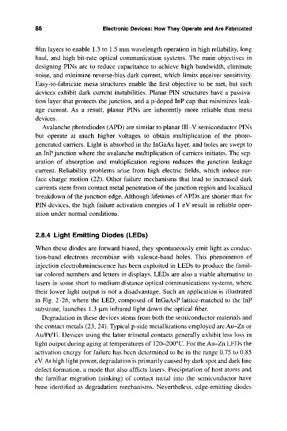
86 Electronic Devices: How They Operate and Are Fabricated
film layers to enable 1.3 to 1.5 mm wavelength operation in high reliability, long haul, and high bit-rate optical communication systems. The main objectives in designing PINs are to reduce capacitance to achieve high bandwidth, eliminate noise, and minimize reverse-bias dark current, which limits receiver sensitivity. Easy-to-fabricate mesa structures enable the first objective to be met, but such devices exhibit dark current instabilities. Planar PIN structures have a passiva-tion layer that protects the junction, and a p-doped InP cap that minimizes leak-age current. As a result, planar PINs are inherently more reliable than mesa devices.
Avalanche photodiodes (APD) are similar to planar III-V semiconductor PINs but operate at much higher voltages to obtain multiplication of the photo-generated carriers. Light is absorbed in the InGaAs layer, and holes are swept to an InP junction where the avalanche multiplication of carriers initiates. The sep-aration of absorption and multiplication regions reduces the junction leakage current. Reliability problems arise from high electric fields, which induce sur-face charge motion (22). Other failure mechanisms that lead to increased dark currents stem from contact metal penetration of the junction region and localized breakdown of the junction edge. Although lifetimes of APDs are shorter than for PIN devices, the high failure activation energies of 1 eV result in reliable oper-ation under normal conditions.
2.8.4 Light Emitting Diodes (LEDs)
When these diodes are forward biased, they spontaneously emit light as conduc-tion-band electrons recombine with valence-band holes. This phenomenon of injection electroluminescence has been exploited in LEDs to produce the famil-iar colored numbers and letters in displays. LEDs are also a viable alternative to lasers in some short to medium distance optical communications systems, where their lower light output is not a disadvantage. Such an application is illustrated in Fig. 2-26, where the LED, composed of InGaAsP lattice-matched to the InP substrate, launches 1.3 |Lim infrared light down the optical fiber.
Degradation in these devices stems from both the semiconductor materials and the contact metals (23, 24). Typical p-side metallizations employed are Au-Zn or Au/Pt/Ti. Devices using the latter trimetal contacts generally exhibit less loss in light output during aging at temperatures of 120-200°C. For the Au-Zn LEDs the activation energy for failure has been determined to be in the range 0.75 to 0.85 eV. At high light power, degradation is primarily caused by dark spot and dark line defect formation, a mode that also afflicts lasers. Precipitation of host atoms and the familiar migration (sinking) of contact metal into the semiconductor have been identified as degradation mechanisms. Nevertheless, edge-emitting diodes
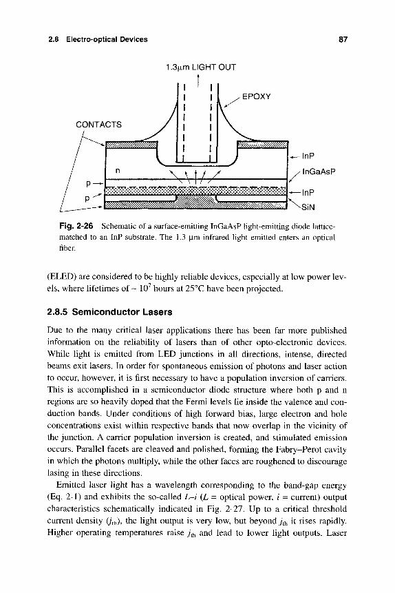
2.8 Electro-optical Devices 87
1.3fxm LIGHT OUT
EPOXY
CONTACTS
Fig. 2-26 Schematic of a surface-emitting InGaAsP light-emitting diode lattice-matched to an InP substrate. The 1.3 jim infrared light emitted enters an optical fiber.
(ELED) are considered to be highly reliable devices, especially at low power lev-els, where lifetimes of ~ 10^ hours at 25°C have been projected.
2.8.5 Semiconductor Lasers
Due to the many critical laser applications there has been far more published information on the reliability of lasers than of other opto-electronic devices. While light is emitted from LED junctions in all directions, intense, directed beams exit lasers. In order for spontaneous emission of photons and laser action to occur, however, it is first necessary to have a population inversion of carriers. This is accomplished in a semiconductor diode structure where both p and n regions are so heavily doped that the Fermi levels lie inside the valence and con-duction bands. Under conditions of high forward bias, large electron and hole concentrations exist within respective bands that now overlap in the vicinity of the junction. A carrier population inversion is created, and stimulated emission occurs. Parallel facets are cleaved and polished, forming the Fabry-Perot cavity in which the photons multiply, while the other faces are roughened to discourage lasing in these directions.
Emitted laser light has a wavelength corresponding to the band-gap energy (Eq. 2-1) and exhibits the so-called L-i (L = optical power, / = current) output characteristics schematically indicated in Fig. 2-27. Up to a critical threshold current density (/th), the light output is very low, but beyond jth it rises rapidly. Higher operating temperatures raise y'th and lead to lower light outputs. Laser
88 Electronic Devices: How They Operate and Are Fabricated
LIGHT OUTPUT
(L)
DRIVE CURRENT (/)
Fig. 2-27 Assorted laser light output current characteristics depicted schematically. From reference 25.
diodes displaying the kinked and nonlinear characteristics shown in Fig. 2-27 are considered to be faulty (25). Peaked kinks are often, but not always, indicative of internal defects and damage, while internal reflections frequently, but not always, cause the second type of kink characteristics. Kinks are also associated with higher-order modes of laser emission and changes in 7th-
The simplest of all laser structures, the homojunction configuration, contains the same semiconductor material, e.g., GaAs, on both sides of the junction. Good only as a pedagogical tool, such lasers require enormous threshold current densi-ties (-50 kA/cm^ at 300K and ~5 kA/cm^ at 77K) to initiate lasing. The severe reliability problems implied by Joule heating thus rule out continuous homojunc-tion laser operation at room temperature. Furthermore, carriers can wander from the active region and recombine, resulting in a broadened emission. Output light stems from a considerably narrower active region in double-heterojunction lasers. First, the carriers are confined by the two heterojunction GaAs and Alj,Gai_j,As barriers. Second, light is confined to the active region by virtue of the higher index of refraction of GaAs relative to AlGaAs. Both effects lower the lasing threshold an order of magnitude, while narrow stripe contacts (20 jim wide) reduce y'th fur-ther, to the point where reliable continuous operation can occur at room tempera-ture. The evolution of these GaAs-based lasers, designed to operate in the range 0.8-0.9 |im, is depicted in Fig. 2-28.
Popular laser geometries for optical communication systems are shown in Fig. 2-29 and employ InGaAsP semiconductor materials (25). Known as BH or buried-heterojunction lasers, the light generated in the buried active regions is
2.8 Electro-optical Devices 89
METAL CONTACT
p-GaAs
n-GaAs
CONTACT-
p-AlxGa-|.xAs
p-GaAs
n-AlxGai.xAs
METAL
OXIDE
p+-GaAs
p-AlxGa-j.xAs
p-GaAs
n-AlxGa-j.xAs GaAs
SUBSTRATE
(a)
(c)
Fig. 2-28 Evolution of GaAs-based lasers, designed to operate in the range 0.8-0.9 jim. From S.M. Sze, Semiconductor Devices, Physics and Technology, J. Wiley and Sons, New York (1985), Copy-right by Bell Telephone Laboratories, Inc.
strongly guided in these devices. Other features include low threshold currents and high quantum efficiencies. Instead of using only the reflective facets for con-trolling light output, an extended diffraction grating is incorporated in so-called distributed feedback (DFB) lasers for this purpose. In this way a single laser wavelength from the multipeaked laser output can be selected and amplified.
A number of failure modes commonly observed in lasers include damage to facets, dark line and dark spot defect formation, aging effects, electrostatic
90 Electronic Devices: How Tliey Operate and Are Fabricated
p-lnGaAsP n-lnP
p-lnP
Contact
InGaAsP Active Region
Si02 Insulator
p-lnGaAs p-lnP n-lnP p-lnP
n-lnP
p+-lnGaAsl
InGaAsP Active Region
M Shifted 1st Order Grating
InGaAsP Active Region
n-lnGaAsP Guiding Region
Fig. 2-29 Popular laser geometries for optical communi-cation systems. Top: Etched mesa buried heterostructure (EMBH). Middle: Channeled substrate buried heterostruc-ture (CSBH). Bottom: Double channel planar buried het-erostructure distributed-feedback. From reference 25.
discharge, and current-confinement problems. The latter are manifested as a drop in laser efficiency because current leaks or is shunted away from the active region. Poor design, processing, and power surges are often the cause of current-confinement problems, to which some laser structures are more prone than oth-ers. Interestingly, InGaAsP lasers have a higher immunity to laser degradation effects than AlGaAs/GaAs-type lasers.
2.9 Processing-—The Chip Level 91
Detailed mechanisms for the failure of lasers and other electro-optical devices and components will be presented in Chapter 10.
2.9 PROCESSING—THE CHIP LEVEL
2.9.1 Introduction
It is much easier to draw schematics of devices and IC circuit diagrams on paper or with the aid of computers than to realize them in physical terms. The produc-tion of devices requires different electrical materials to be shaped or patterned and creatively merged to form the active devices and passive components that must then be interconnected, insulated, and finally packaged. These issues and demands are at the core of a very broad interdisciplinary manufacturing technol-ogy that designs, fabricates, and packages solid-state devices and circuits.
Much of the glamour associated with semiconductor manufacturing occurs on the Si chip level, and that is what we shall address here. To appreciate what is involved, consider the state-of-the-art CMOS technology employed in the fabrica-tion of advanced microprocessor chips. At the base of the stunning image of Fig. 2-30, beneath the skeleton of the exposed interconnects, contacts, and first aluminum wire level, are the CMOS transistors. These MOSFETs have effective channel lengths of 0.25 |im and gate-oxide thicknesses of 7.7 nm (26).
Fig. 2-30 Scanning electron microscope image of the local interconnect and first-level aluminum wires in an SRAM cell. From reference 26.
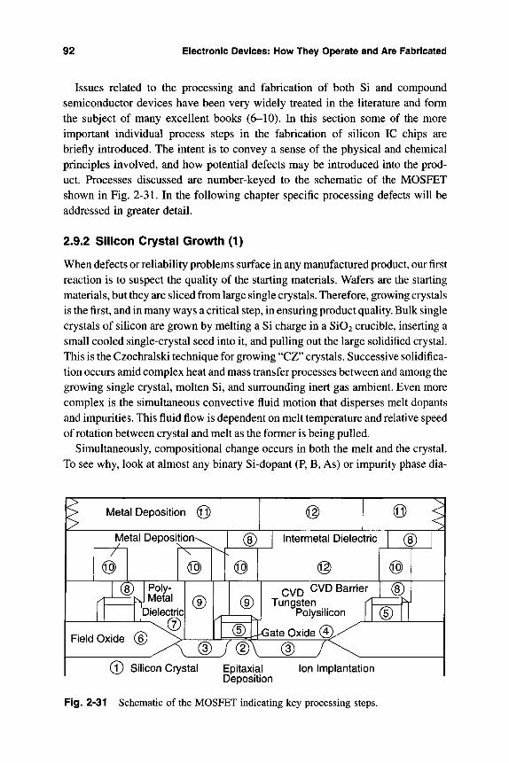
92 Electronic Devices: How They Operate and Are Fabricated
Issues related to the processing and fabrication of both Si and compound semiconductor devices have been very widely treated in the literature and form the subject of many excellent books (6-10). In this section some of the more important individual process steps in the fabrication of silicon IC chips are briefly introduced. The intent is to convey a sense of the physical and chemical principles involved, and how potential defects may be introduced into the prod-uct. Processes discussed are number-keyed to the schematic of the MOSFET shown in Fig. 2-31. In the following chapter specific processing defects will be addressed in greater detail.
2.9.2 Silicon Crystal Growth (1)
When defects or reliability problems surface in any manufactured product, our first reaction is to suspect the quality of the starting materials. Wafers are the starting materials, but they are sliced from large single crystals. Therefore, growing crystals is the first, and in many ways a critical step, in ensuring product quality. Bulk single crystals of silicon are grown by melting a Si charge in a Si02 crucible, inserting a small cooled single-crystal seed into it, and pulling out the large solidified crystal. This is the Czochralski technique for growing "CZ" crystals. Successive solidifica-tion occurs amid complex heat and mass transfer processes between and among the growing single crystal, molten Si, and surrounding inert gas ambient. Even more complex is the simultaneous convective fluid motion that disperses melt dopants and impurities. This fluid flow is dependent on melt temperature and relative speed of rotation between crystal and melt as the former is being pulled.
Simultaneously, compositional change occurs in both the melt and the crystal. To see why, look at almost any binary Si-dopant (P, B, As) or impurity phase dia-
Metal Deposition @ ® Metal Deposition-
"7^ Intermetal Dielectric ®
® QYQ CVD Barrier I (§)
Tungsten Polysilicon
iir®v IXoaXe Oxide @
(T) Silicon Crystal Epitaxial Ion Implantation Deposition
Fig. 2-31 Schematic of the MOSFET indicating key processing steps.
2.9 Processing—The Chip Levei 93
gram. Note that the liquidus and soHdus phase boundary lines drop for small solute additions. Equilibrium at the crystal-melt growth interface implies that the solid is always purer than the liquid. Since the effect is cumulative during direc-tional solidification, axial gradients in composition are predicted (27). Grown crystals not only exhibit varying concentration profiles of intentionally added dopants, but contain unwanted elements like oxygen. But it is the transition metal impurities that are viewed with particular alarm; they cause the most severe prob-lems, and great efforts are made to eliminate them or neutralize their influence. In addition, defect swirl patterns are not infrequently observed on planes sliced per-pendicular to the crystal axis. Furthermore, surface striations that are several microns wide and alternately dopant rich and dopant poor sometimes decorate the length of bulk Si and compound semiconductor single crystals. Both features apparently stem from temperature fluctuations at the growth interface and com-plex convective flow patterns that cause a periodic partitioning of solute. From the standpoint of the MOSFET, variations in dopant level across the plane of a wafer must be minimized to ensure uniform device processing and chip performance.
Following growth, the crystals are shaped round by grinding and then sawed and polished to produce wafers. Presently, integrated circuit production lines process 15 to 20 cm diameter Si wafers, but huge 30 cm diameter wafers are expected to become the world standard shortly after the turn of the twenty-first century.
2.9.3 Epitaxy (2)
This important term refers to the ordered crystallographic registry of a single crys-tal film deposit on an underlying crystalline substrate template. If film and sub-strate are the same (Si on Si) we speak of homoepitaxy. In electro-optical devices they are different (InGaAsP on InP), and heteroepitaxy is the appropriate term. The yield of early thin-film bipolar transistors fabricated within homoepitaxially deposited Si was dramatically improved relative to those produced within the original, or uncoated. Si wafers. Chemical vapor deposition (CVD) or some vari-ant of it is used to deposit epitaxial semiconductor films on wafer substrates. The process typically entails reaction of a chlorinated silane, e.g., SiCl4, and H2 at tem-peratures of ~1100°C and a pressure of ~1 atm. Epitaxial processing in CMOS technology helps assure device isolation and minimizes junction leakage currents.
Critical to insuring single crystal formation is a combination of a low film nucleation rate and a high film growth rate. If many nuclei form on the substrate, a worthless polycrystalline film deposits. A low gas supersaturation and deposi-tion rate will create few nuclei. On the other hand, high substrate temperatures enhance diffusion rates and facilitate atomic incorporation into lattice sites. This promotes the early lateral extension of the single crystal film, and growth per-fection as it thickens. Epitaxial Si films are purer and frequently more defect-free
94 Electronic Devices: How They Operate and Are Fabricated
than the substrate wafer; furthermore, they can be doped independently of it. Nevertheless, they do contain the assorted point, line, and surface defects noted later in Fig. 3-15 that occasionally cause device malfunction.
2.9.4 Ion Implantation (3)
For high-performance devices with shallow junction depths, ion implantation, rather than diffusion, is the preferred method of doping. Unlike diffusion, where the surface dopant concentration is higher than in the crystal interior, the reverse is true in ion implantation. The subsurface wafer penetration of dopant ions is due to energies of -50-200 keV acquired when they are accelerated in the high electric field of the implanter. Possessing energies thousands of times larger than the binding energy of lattice atoms, the dopant ions wreak havoc as they are embedded into Si. At first a lightning-like ion current excites the atomic elec-trons and ionizes atoms, absorbing energy in the process. When the dopants lose enough energy, they slow sufficiently and then begin to violently collide with Si nuclei, knocking many off their lattice sites. Each dopant ion executes a differ-ent odyssey and comes to rest at a different distance from the wafer surface. Spa-tially, dopant concentrations are statistically distributed as a Gaussian function both normal to the surface and transverse to it. The depth of the peak and spread of the Gaussian depends on the dopant and the nature of the matrix it passes through, e.g.. Si, Si02, SiN, photoresist. Ion beam damage to the silicon matrix creates disordered and even amorphous regions. These must be repaired by rapid thermal annealing at ~900°C, where atoms can diffuse sufficiently to restore lat-tice crystallinity and full electrical activity to the dopants.
In modem IC chips some 15 to 20 or more ion implantation steps are carried out to dope large volumes (tubs), small regions (sources and drains), and to adjust the threshold voltage of field effect transistors. This latter operation, which controllably alters the interface charge (Q^ in Eq. 2-6) at the Si-Si02 boundary, is quite critical and requires precise ion doses and spatial distributions. Tailoring dopant profiles by ion implantation has additionally enabled mini-mization of hot-electron damage and latchup effects, as well as gettering of heavy metal (Fe) contaminants. In the latter two cases, high-energy implants are required to drive dopants deep beneath the surface layer of devices.
Ion implanters are one of the most complex pieces of microelectronics pro-cessing equipment; they are also potential and actual sources of contamination and defects. Ideally, a chemically pure, monoenergetic beam is desired. In a practical sense one may imagine defects arising from variations in ion beam energy, depth, lateral spatial distribution and ion dose, as well as from the pres-ence of chemical contaminants. Examples are given in Chapter 3.

2.9 Processing—The Chip Levei 95
All of the processes to this point have been concerned with the underlying Si. Above the Si surface are assorted grown and deposited dielectric and conducting films that we now consider.
2.9.5 Gate Oxide (4)
Today's ULSI technology is due in large part to the excellent properties of ther-mally grown gate oxides. This critical Si02 film, the smallest fabricated dimen-sion in MOS devices, has been the focus of much study and reliability testing. Currently, less than 10 nm thick, it is made by controllably oxidizing silicon wafers in dry O2. The simple reaction. Si + O2 ^ Si02, at temperatures between 900 and 1100°€, produces a dense amorphous film. Thick oxide growth has tra-ditionally been modeled by linear kinetics at short time (i.e., d^ ~ t) and by par-abolic kinetics at long time, i.e., d^ ~ t^'^, where d^ is the oxide thickness and t is the time. These formulas may not hold for the very thin oxides now grown.
Growth in the presence of N2O is a recent advance that has improved the qual-ity of gate oxides. Nitrided oxides are apparently more resistant to (charge) trap generation and to plasma-induced charging, give rise to smaller electric-field-induced leakage cuia-ents, and are generally longer lived than conventional oxides (28, 29). Oxide charging during operation, and the associated reliability problems of breakdown and hot electron degradation are topics discussed in Chapter 6.
2.9.6 Polysilicon (5)
The gate oxide is contacted by a polysilicon electrode. Long ago, polysilicon replaced the much more unreliable aluminum electrodes that caused early dielec-tric breakdown in underlying oxides. Polysilicon films are deposited in low-pressure CVD reactors through the reduction of silane by hydrogen. Below ~590''C amorphous films form, while above ~610°C polycrystalline films deposit. This narrow temperature range defines a useful processing window. At higher temperatures, gas phase reactions result in rough, loosely adhering deposits and silane depletion that causes poor film uniformity. Impracticably low deposition rates occur at lower temperatures.
2.9.7 Deposited and Etched Dielectric Films (6,7,12)
Since all devices and interconnections support voltages and carry current while sitting on a conducting Si wafer, strategically placed dielectrics are needed to isolate them electrically. Aside from the critical (grown) gate oxide, an assort-ment of other insulator films are deposited. They include Si02, silicon nitride, and phospho- and boro-silicate glasses produced by CVD methods, often with the assistance of a plasma discharge. The dielectric films must then be etched to
96 Electronic Devices: How Tliey Operate and Are Fabricated
expose windows to semiconductor contacts or to confine subsequently deposited metal films and vias (see next section). After microelectronic chips are fabricated they are usually encapsulated by a silicon nitride film, an effective barrier that prevents moisture and alkali ion (Na" ) penetration. All of the above dielectrics are amorphous in structure and of the order of 1 |Lim thick. Typical reactions with precursor gases (on the left) and product films (on the right) include:
for Si02, Si (OC2H5)4 (TEOS) -^ SiOz + byproducts at 700°C
for silicon nitride, 8NH3 + 3Si2Cl2H2 -> 2Si3 N4 + 6HC1 + I2H2 at ~ 750°C
SiH4 + NH3 -> SiNH + 3H2 at 300°C
for phosphosilicate glass,
SiH4 + 4PH3 + 6O2 -> Si02 - 2P2O5 + 8H2 at 450°C
In general, dielectric film deposition steps are carried out at successively lower temperatures so as not to alter the prior processed and doped materials.
The composition, structure, and properties of such CVD films vary widely with deposition conditions. Silicon nitride is an example. At very high tempera-tures dense, crystalline Si3N4 forms, but at lower temperatures considerable hydrogen is incorporated, particularly during plasma assisted deposition. Differ-ences in dielectric strength, internal stress, and resistance to permeation of water and ionic impurities occur, but generally not to the point of compromising relia-bility. High phosphorous or arsenic glass compositions also corrode aluminum lines when moisture is present. More significant are the problems associated with surface coverage by dielectric films and maintaining a planar terrain for subsequent metal depositions. Incomplete filling of deep trenches and regions between metal lines can lead to structural voids and occasional short circuiting.
Maintaining a planar topography is extremely important if subsequent lithog-raphy patterning errors and defects in deposited structures are to be avoided. The relatively new technique of chemical-mechanical polishing (CMP) has enabled the production of planar interfaces between successive metal and intermetal dielectric levels.
2.9.8 Metallization (8-11)
There is a need to contact and interconnect all of the doped semiconductor elec-trodes, i.e., source, drain, and gate, to other components and devices on the chip. Assorted metal and alloy conductors are employed for contact structures includ-ing Al and Al-Si, PtSi, Ti-W, Pd2Si, TiSi2. Interconnections, on the other hand, are invariably composed of Al thin-film alloys with dilute Cu or Cu-Si additions. In high-density ICs, efficient packing of devices on the chip real estate requires
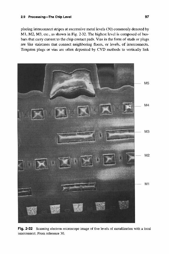
2.9 Processing—The Chip Level 97
placing interconnect stripes at successive metal levels (30) commonly denoted by Ml, M2, M3, etc., as shown in Fig. 2-32. The highest level is composed of bus-bars that carry current to the chip contact pads. Vias in the form of studs or plugs are like staircases that connect neighboring floors, or levels, of interconnects. Tungsten plugs or vias are often deposited by CVD methods to vertically link
M5
M4
M3
M2
M1
Fig. 2-32 Scanning electron microscope image of five levels of metallization with a local interconnect. From reference 30.
98 Electronic Devices: How They Operate and Are Fabricated
adjacent interconnect levels. As shown in Fig. 2-31, these vias are surrounded by TiN barrier films that prevent mobile ions from reaching sensitive junctions and reactive gases from etching exposed oxides. The above metals possess the best collective basket of desirable properties, including 1. high electrical conductivity; 2. low contact resistance to Si; 3. little tendency to chemically react with or inter-diffuse in Si; 4. resistance to corrosion and environmental degradation; 5. electro-migration resistance; 6. ease of deposition; 7. compatibility with other materials and steps in the fabrication process.
The physical vapor deposition (PVD) techniques of evaporation and sputter-ing are the means employed to deposit metal films. Sequential atom-by-atom deposition results in film nucleation and subsequent growth. Unlike epitaxial deposition, both methods yield polycrystalline films typically having submicron grain sizes, due in part to substrates that are often amorphous (e.g., Si02).
Evaporation is the simpler of these metallization methods and involves heat-ing of the source metal until it evaporates at appreciable rates. The process is carried out in high vacuum while wafer substrates, carefully positioned relative to the evaporation source, are rotated to yield uniform metal coverage. In sput-tering, the metal or alloy to be deposited is fashioned into a cathode plate elec-trode and generally placed parallel to the wafers (anode) within a chamber con-taining inert sputtering gas. At low pressures less than ~5 mTorr, and potential differences of a few kilovolts dc, a glow discharge is sustained between elec-trodes. Within the discharge, energetic positive gas ions bombard the target, dis-lodging atoms that then deposit on the wafers as a film. In magnetron sputtering, magnets placed behind the cathode confine electrons to hop around the target and create a richer plasma that increases film deposition rates.
The two metallization processes compete in many applications, and not only in semiconductor technology, but other industries as well. Issues that must be considered in selecting the best one for a particular application include 1. adhe-sion to the substrate; 2. film stress; 3. stoichiometry of alloys films; 4. uniform coverage of the topography; and 5. electrical damage to substrate oxides. Sput-tering is preferred in most semiconductor applications because stoichiometry of alloys is maintained and step coverage is usually superior. However, evaporated Al films appear to be more resistant to electromigration damage.
Many reliability problems are associated with contact and interconnection metallizations. They include changes in contact resistance due to interdiffusion reactions between Al and Si, electromigration-induced degradation of contacts and interconnections, and general corrosion damage. Contacts between Si and Al, two indispensible elements in microelectronics, are particularly troublesome. This results from mutual atomic interdiffusion (Section 5.4.2) and is remedied through alloying (e.g., Al-l%Si) or the use of diffusion barriers (e.g., metal sili-
2.9 Processing—The Chip Level 99
cides, TiW). These must be imposed between the silicon and Al interconnec-tions to prevent reaction. Other problems stem from stress. When surrounded on all sides by oxide, as interconnects are in the various metallization levels, tensile stresses develop in the metal. The reason, as we shall see in the next chapter, is due to the larger thermal expansion coefficient of Al relative to Si02. These thermal stresses are sometimes sufficiently large to generate voids that open interconnects.
2.9.9 Plasma Etching
Plasma processes are widely employed in the fabrication of semiconductor devices. Examples include plasma-enhanced CVD, photoresist removal, and the etching of polysilicon, dielectric, and metal thin films. Within the plasma a very reactive environment consisting of high energy electrons, ions, and precursor gas free radicals is created by applied voltages of a few kV. This combination of ener-getic reactants speeds up otherwise sluggish vapor deposition or material removal (etching) reactions, and effectively makes them proceed at lower temperatures. In our MOSFET, the need to etch contacts and vias in Si02 is met by radio-frequency (RF) plasmas employing process gases containing fluorine, carbon, and oxygen. Minimum dimensions, high aspect ratio features, and selectivity of the etch are necessary attributes of the etching process. The last attribute requires that neigh-boring polysilicon, metal, or silicides be immune to etching attack.
Damage to materials during plasma etching includes the buildup of charge and dielectric wearout due to bond breaking and charge trapping.
2.9.10 Lithography
Perhaps the most critical process in microelectronics is lithography, a technology that embodies a collection of critical steps. Lithography involves the use of expo-sure tools, masks, resist materials, and etching processes to enable such blanket-area processing steps as film deposition, etching, diffusion, and ion implantation to effectively occur only in preselected areas of a wafer surface. While there are obvious parallels to photography, instead of producing flat images on paper, a three-dimensional relief topography is created in materials like Si, Si02, silicon nitride, aluminum, and photoresist. After a mask (reticle) is generated with the desired geometric features, lithographic patterning involves spinning a photore-sist film on the wafer surface. As the name implies, photoresists are sensitive to photons and resistant to chemical attack by liquid or gaseous etchants. Some are also sensitive to electrons and X-rays. In general, they consist of specially com-pounded polymers and display two broad types of behavior. When exposed to light, the cross-linked polymer chains of positive resists undergo scission, or cut-
100 Electronic Devices: How They Operate and Are Fabricated
ting, rendering them more soluble in a developer, while unexposed areas resist chemical attack. Under the same stimulus, negative resist molecules polymerize, while unexposed regions are soluble and dissolve in the developer.
If, for example, it is desired to dope silicon, a blanket film of Si02 is first deposited and then covered with a photoresist layer. After exposure and devel-opment, the unprotected Si02 film is removed by etching, and the photoresist is stripped away. This leaves the bare Si surface geometrically patterned by the remaining Si02 film mask. Now the exposed Si regions may be ion implanted. Similar steps must be repeated at many different depths, or levels, on the wafer as actual integrated circuits unfold. Alignment of successive levels, e.g., contact metal over a contact hole, is absolutely critical so that correct registry is main-tained simultaneously over millions of device features on large wafers. The mag-nitude of the problem can be appreciated when it is understood that 10 to 20 lith-ography levels are required in advanced IC chips.
Poor product yields have often been associated with lithography defects. These arise predominantly from mask pattern defects that are discussed in Sect. 3.4.2.4. Metallization patterns defined after etching may then, for example, con-tain either missing or added metal, which results in open or shorted conductors, respectively. Mask defects can be more readily tolerated by the expedient of employing 5x or lOx reduction stepper tools that project the patterns onto pho-toresists. The Ix systems do not offer this opportunity and therefore require more defect-free masks.
EXERCISES
2-1 What are some differences between materials used for electrically and mechanically functional applications?
2-2 Metals are the best conductors of electricity and heat, reflect light most efficiently, and are the most malleable of materials. Explain these attributes of metals in terms of their electronic and atomic structure.
2-3 Copper wiring in a telephone switching station was exposed to a fire. After the fire the electrical resistivity of the wiring was measured. Some wiring was observed to have a lower resistivity, while other wiring exhibited an increase in resistivity. a. Describe a scenario that would result in a resistivity decrease. b. Describe a scenario that would result in a resistivity increase.
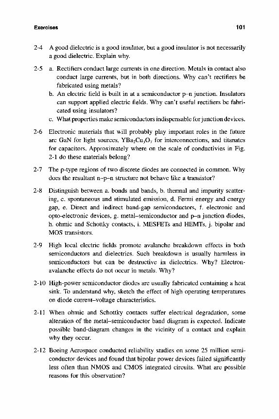
Exercises 101
2-4 A good dielectric is a good insulator, but a good insulator is not necessarily a good dielectric. Explain why.
2-5 a. Rectifiers conduct large currents in one direction. Metals in contact also conduct large currents, but in both directions. Why can't rectifiers be fabricated using metals?
b. An electric field is built in at a semiconductor p-n junction. Insulators can support applied electric fields. Why can't useful rectifiers be fabri-cated using insulators?
c. What properties make semiconductors indispensable for junction devices.
2-6 Electronic materials that will probably play important roles in the future are GaN for light sources, YBa2Cu307 for interconnections, and titanates for capacitors. Approximately where on the scale of conductivies in Fig. 2-1 do these materials belong?
2-7 The p-type regions of two discrete diodes are connected in common. Why does the resultant n-p-n structure not behave like a transistor?
2-8 Distinguish between a. bonds and bands, b. thermal and impurity scatter-ing, c. spontaneous and stimulated emission, d. Fermi energy and energy gap, e. Direct and indirect band-gap semiconductors, f. electronic and opto-electronic devices, g. metal-semiconductor and p-n junction diodes, h. ohmic and Schottky contacts, i. MESFETs and HEMTs, j . bipolar and MOS transistors.
2-9 High local electric fields promote avalanche breakdown effects in both semiconductors and dielectrics. Such breakdown is usually harmless in semiconductors but can be destructive in dielectrics. Why? Electron-avalanche effects do not occur in metals. Why?
2-10 High-power semiconductor diodes are usually fabricated containing a heat sink. To understand why, sketch the effect of high operating temperatures on diode current-voltage characteristics.
2-11 When ohmic and Schottky contacts suffer electrical degradation, some alteration of the metal-semiconductor band diagram is expected. Indicate possible band-diagram changes in the vicinity of a contact and explain why they occur.
2-12 Boeing Aerospace conducted reliability studies on some 25 million semi-conductor devices and found that bipolar power devices failed significantly less often than NMOS and CMOS integrated circuits. What are possible reasons for this observation?
102 Electronic Devices: How They Operate and Are Fabricated
2-13 In a real, or nonideal, MOS capacitor structure, the work functions of the metal and semiconductor differ. Sketch the band structures of an unbiased metal-Si02-p-type Si capacitor if ^u > ^si-b. Illustrate depletion, accumulation and inversion for this structure. c. Sketch the band structures for depletion, accumulation, and inversion in
an ideal metal-Si02-n-type Si capacitor structure.
2-14 One strategy to minimize the probability of latchup in CMOS devices is to fabricate them within a silicon film grown epitaxially on an insulator (SOI). Illustrate how SOI structures suppress latchup.
2-15 Distinguish between the functions of a. Microprocessor and memory chips, b. DRAMs and SRAMs, c. Charge-coupled devices and DRAMs, 4. Gate capacitor and trench capacitor.
2-16 When zero bias is apphed in the HEMT structure, the conduction band edge in the GaAs Ues below the Fermi level, implying a large density of the 2-D electron gas. a. What do you expect to happen when the gate is biased negatively? b. Draw band diagrams for both zero and negative bias.
2-17 When compared to silicon device technology, compound-semiconductor laser production involves may fewer steps and generally more art. If this is so, what are the reliability implications of such products?
2-18 Some polymers degrade upon exposure to radiation due to bond breaking. Covalent bond energies for some important atomic pairings are: Bond pair Energy (kJ /mol) Bond pair Energy (kJ /mol) C-C 340 C-H 420 C-C 620 C-Cl 330 What portion of the electromagnetic spectrum would be expected to cause radiation-damage effects in each bond type?
2-19 Damage to opto-electronic devices and materials often stems from recom-bination of electron-hole pairs without photon emission (nonradiative recombination) and from self-absorption of the involved radiation. Explain how each phenomenon could cause degradation.
REFERENCES
1. S. M. Sze, Semiconductor Devices—Physics and Technology, Wiley, New York (1985).

References 103
2. B. G. Streetman, Solid State Electronic Devices, 4th ed.. Prentice Hall, Engelwood Cliffs, NJ (1995).
3. J. M. Mayer and S. S. Lau, Electronic Materials Science—For Integrated Circuits in Si and GaAs, Macmillan, New York (1990).
4. A. Bar-Lev, Semiconductors and Electronic Devices, 3rd ed.. Prentice Hall, Engelwood Cliffs, NJ (1993).
5. T. M. Fredericksen, Intuitive IC Electronics, 2nd ed. McGraw Hill, New York (1989).
6. S. M. Sze, ed. VLSI Technology, 2nd ed., McGraw Hill, New York (1988). 7. S. Middleman and A.K. Hochberg, Process Engineering Analysis in Semi-
conductor Device Fabrication, McGraw Hill, New York (1993). 8. W. S. Ruska, Microelectronic Processing, McGraw Hill, New York (1987). 9. G. E. Anner, Planar Processing Primer, Van Nostrand Reinhold, New York
(1990). 10. R. C. Jaeger, Introduction to Microelectronic Fabrication, volume V, Addi-
son-Wesley, Menlo Park, CA (1988). 11. A. A. Iranmanesh and B. Bastani, IEEE Circuits and Devices 8 (3), 14
(1992) 12. E. Adler et. al., IBM / . Res. and DeveL 39 (1/2), 167 (1995). 13. H. E. Mass, G. Groeseneken, H. Labon, and J. Witters, Microelectronics
Journal 20, 9 (1989). 14. W. T. Anderson, Tutorial Notes, IEEE International Reliability Physics Sym-
posium, l.l (1992). 15. W. J. Roesch, Tutorial Notes, IEEE International Reliability Physics Sym-
posium, 1.1 (1988). 16. A. Christou, Tutorial Notes, IEEE International Reliability Physics Sympo-
sium, 3.1 (1986). 17. H. Morkoc, IEEE Circuits and Devices 7, 15 (1991). 18. F. Magistrali, C. Tedesco, E. Zanoni, and C. Canali, in Reliability of Gallium
Arsenide MMICs, ed. by A. Christou, Wiley, Chichester (1992). 19. K. Wilson, GEC J, Res, 4, 126 (1986). 20. A. Bensoussan, P. Coval, W. J. Roesch, and T. Rubalcava, 32nd Annual Pro-
ceedings of the IEEE Reliability Physics Symposium, p. 434 (1994). 21. C. R Skrimshire, J. R. Farr, D. F. Sloan, M. J. Robertson, R A. Rutland, J. C.
D. Stokoe, and R. R. Sutherland, lEE Proceedings, 137, PtJ, No 1, 74 (1990). 22. S. P. Sim, Semiconductor Device Reliability, ed. by A. Christou and B. A.
Unger, Kluwer, Amsterdam (1990). 23. M. Fukuda, IEEE J. Lightwave TechnoL 6, 1488 (1988) 24. M. Fukuda, Reliability and Degradation of Semiconductor Lasers and
LEDs, Artech, Boston (1991).
104 Electronic Devices: How Tliey Operate and Are Fabricated
25. J. Spencer and R. Koelbl, Tutorial Notes, IEEE International Reliability Physics Symposium, 1.1 (1989).
26. R. W. Mann, L. A. Clevinger, R D. Agnello, and F. R. White, IBM J. Res, and Develop. 39, 403 (1995).
27. W. Zulehner in Semiconductor Silicon, ed. G. Harbeke and M. J. Schulz, R2, Springer Veriag, Berlin (1989).
28. A. B. Joshi, R. Mann, L. Chung, M. Bhat, H. T. Cho, B. W. Min, and D. L. Kwong, 33rd Annual Proceedings of the IEEE Reliability Physics Sympo-sium, p. 156 (1995).
29. C. Felsch and E. Rosenbaum, 33rd Annual Proceedings of the IEEE Relia-bility Physics Symposium, p. 142 (1995).
30. J. G. Ryan, R. M. Geffken, N. R. Poulin and J. R. Paraszczak, IBM J, Res. and Develop. 39, 371 (1995).
31. J. A. Reynolds, Solid State Tech. 37, No 12, 63 (1994).
Chapter 3
Defects, Contaminants and Yield
3.1 SCOPE
There are defects and DEFECTS, and there are K I L L E R D E F E C T S ! ! From the relatively innocuous to those that immediately disqualify an IC chip, this chapter is largely concerned with the nature of defects, their generation dur-ing processing, strategies used to minimize their influence, and how they adversely influence product yield. The harmful effects of crystallographic defects is strongly dependent on the nature of the material they inhabit. For example, metals are usually far more tolerant of point defects, dislocations, and grain boundaries (GB) than are semiconductors. Whereas semiconductors must be free of dislocations and GBs, metallizations contain these in relatively large densities with little ill effect. And, since the matrices of most ceramics used in microelectronics are already amorphous or fine-grained, these same crystallo-graphic defects usually affect properties only marginally.
At the next level there are DEFECTS that represent gross deviations in the structural and chemical integrity of the material over macroscopic dimensions. They include voids, precipitates, missing structural features because of litho-graphic errors, deformed or even cracked structures due to stress, and particulate contaminants. Such defects may or may not cause devices or ICs to immediately fail inspection, and might or might not be a source of reliability problems.
105
106 Defects, Contaminants and Yield
KILLER DEFECTS, however, immediately cause rejection of the prod-uct. It does not take a very large defect to become a killer defect if it is strategically located, such as at a semiconductor junction or on a lithography mask. The most troubling aspect is that as circuit features continue to get ever smaller, killer defect sizes shrink in concert. As a rough guide, the "1/3 rule" (1) suggests that the killer defect size scales as one-third the minimum feature size.
The general problem of defects can be put into perspective by considering DRAM chips, the primary driver of microelectronics technology. On the basis of the 1/3 rule, the killer defect size is estimated to be -0.14 |im in 4Mb DRAMs (1989), ~0.11 |im in 64Mb DRAMs (1994), and only 0.06 |im for 256Mb DRAMs (2000). About 500 distinct processing steps are now required to pro-duce advanced DRAM chips. Among these are over 20 lithographic steps, which must be carried out in a manner such that production yields of chips passing final inspection are high. At every step in the process there are obstacles that have the potential to cause defective products.
Concern over processing defects is perhaps the chief technical preoccupation of manufacturing industries. Survival in the marketplace often hinges on identi-fying defects and developing and implementing strategies to eliminate them. Defects are intrinsic to processing, and a process devoid of defects does not yet exist.
In what must be regarded as one of the more important chapters in the book, aspects of integrated-circuit manufacturing are explored again with particular emphasis placed on processing defects and their consequences. Defects not only influence production costs directly, but reliability concerns more indirectly; those that go undetected in qualified products are like seeds that can sprout under certain circumstances to yield a bitter reliability harvest.
This chapter starts by introducing crystallographic defects and their role in Si and GaAs. Subsequent topics continue the treatment of chip-level process-ing introduced at the end of Chapter 2, paying particular attention to cata-loging processing defects. Specific examples are incorporated explaining the role of stress and highlighting the deleterious role of ubiquitous contaminants. Lastly, the integrated statistical effect of defects on process and product yield is modeled.
While it is impossible to carry out manufacturing processes without incorpo-rating defects, the latter are for the most part removed by inspection, or by screening. And those that pass into the product are often "cosmetic" and more benign in service than the impression sometimes conveyed by this chapter. With this caveat we start with a discussion of defects in crystalline solids and semi-conductors.

3.2 Defects in Crystalline Solids and Semiconductors 107
3.2 DEFECTS IN CRYSTALLINE SOUDS AND SEMICONDUCTORS
3.2.1 General Considerations
All crystalline materials contain intrinsic (lattice) defects such as vacancies, dis-locations, and grain boundaries (GBs). These defects are defined with examples in Table 3-1. For the uninitiated it appears tempting to attribute failures and reli-ability problems in electronic materials to the role of such defects, and at one level such an assumption has validity. In practice, however, the evidence leading from microscopic defects to macroscopic failures is usually very tenuous, and few of the latter can unambiguously be attributed to the former. Complicating matters further are the processing defects, introduced during various steps of the manufacturing sequence. These are grosser in scale than lattice defects and strongly influence yield and malfunction of devices. Returning to lattice defects, the rationale for studying them is to intelligently assess their potential and actual roles as root causes of failures, even though it may be difficult to draw causal relationships.
Table 3-1 Imperfections in Condensed Matter
Classification Definition Examples
Vibrating atom Temporary, small displacement from ideal position
Electronic charge Charge carrier excited from ground-state bond-ing configuration
Chemical impurity Foreign atom of differing size, valence, elec-tronegativity, and/or structure relative to host atoms/structure
Point lattice Missing host atom. Extra host atom. Atom defect occupying wrong lattice site
Nonbridging bond One-dimensional Row of atoms at edge of extra half-plane of defect atoms Two-dimensional Boundary separating an error in stacking defect sequence of atomic planes, boundary between
two crystals of different relative orientation Three-dimensional Macroscopic region of different density, chem-defect ical content, coordination; etc., from host
Zero point, thermal
Electron (-), Hole (+), exciton Substitutional, interstitial
Lattice vacancy, self-interstitial, antisite defect (compounds) (noncrystalline materials) Dislocation (edge and screw) Stacking fault, grain boundary
Void, free volume for glasses, disorder, defect cluster, precipitate
From L. C. Kimerling and J. R. Patel, VLSI Science, Microstructure Science, vol. 12, ed. N. Einspruch, Acade-mic Press, Boston (1985).
108 Defects, Contaminants and Yield
3.2.2 Point Defects
The vacancy or absence of an atom at a lattice site is the most basic defect. Vacancies occur in all classes of solids. In common, the fraction or concentration of vacant lattice sites (Cy) is given by the familiar Boltzmann expression
exp - kr (3-1)
where Ef is the energy required to form a vacancy, i.e., remove an atom from the bulk and place it on the surface. This equation, predicted from thermodynamic considerations, has been experimentally verified in all classes of solids. One of the most damaging effects vacancies exhibit is the formation of voids, usually at an interface between differing materials. Such damage is generally attributed to the condensation of very large numbers of vacancies.
The chief difference between point defects in metals and semiconductors is that the latter are generally electrically active. Charge activity arises from the four dangling severed covalent bonds surrounding the vacancy in the diamond cubic lattice of Fig. 3-1. In contrast, the very mobile free electrons rapidly smooth any charge singularities associated with vacancies in metals.
An initially uncharged vacancy V in a Si lattice can act as an acceptor by acquiring an electron so that it becomes \r. Similarly, it can acquire a positive
Fig. 3-1 Schematic of diamond-cubic lattice and broken bonds around a vacancy (V).
3.2 Defects in Crystalline Solids and Semiconductors 109
charge by combining with a hole and become V . One can also envision neutral vacancies acquiring more than a single net charge, so that V ", V^~, V^'^, V"*", etc. species can exist. Concentrations of such vacancies depend on carrier concentra-tions because vacancy-charge interactions can be viewed from the standpoint of chemical equilibrium, e.g., [V~]/(n[y°] = K. Here we note that n and p are elec-tron and hole concentrations, and that K is the equilibrium constant.
There are an assortment of other defects associated with impurity atoms (Au, FCi, Mo, Ni) or impurity-impurity pairs (Fe—B) that are electrically active in Si. The subscript i denotes an atom occupying an interstitial site. Similar impurity -atom defects have been identified in GaAs (e.g., Fe, Cu) and InP (e.g., Zn). Just as with traditional dopants, these defects have energy levels within the forbidden gap and can act as donors or acceptors. A difference is the much deeper (ioniza-tion) energies in the gap relative to standard dopants. To study such low-defect concentrations (i.e., 10^^-1 O ' /cm ) use has been made of deep level transient spectroscopy, or DLTS. This technique relies on excitation of charge emission from defects located within the capacitance region of a p-n junction and detec-tion of the resulting current decay to equilibrium (2). Significantly, DLTS has been installed in the manufacturing environment to monitor trace contamination during deposition of epitaxial films.
Other semiconductor defects include vacancy-interstitial pairs or Frenkel defects and antisite defects, which occur in 11-Vl and Ul-V compounds. These are characterized, for example, by a Ga atom on an As site within the As sublat-tice, and similarly misplaced As atoms on the Ga sublattice.
3.2.2.1 Effect on Diffusion Point defects play a role in elevated tempera-ture doping, sintering of metal-semiconductor contacts, postannealing of ion implants, and epitaxial deposition. All involve diffusion of atoms, and such processes are complicated in semiconductors. During doping, for example, con-centration-dependent diffusion effects arise that can be attributed to pair interac-tions between charged as well as uncharged vacancies and dopants or impurities. To illustrate the complexity involved, an expression for the extrinsic (impurity) diffusion coefficient (Dgx) is (3)
Dex = A' ' + A"" (P^nO + A " (n/n{) 4- A^" (n/nd^ + A^" (n Ind^. (3-2)
Thus Ax depends on the doping concentration levels that yield n or p, as well as the carrier concentration (^i) in dopant-free or intrinsic Si. In order of appear-ance in Eq. 3-2, the various D^ terms represent the intrinsic diffusivity of impu-rity interaction with . . . neutral point defects, a singly-charged donor point defect, a singly-charged acceptor point defect, a doubly-charged acceptor point defect, and a triply-charged acceptor point defect. Since n and p directly reflect
110 Defects, Contaminants and Yield
the doping concentration (C), this complex expression suggests that D^^ depends nonhnearly on C such that D^^ - C", with a = 1,2,3. . • • Therefore, doping profiles are far more complex than those identified with a linear diffusion theory, where D is independent of concentration (see Sect.5.2).
Examples of anomalous dopant-diffusion effects and profiles are shown in Figs. 3-2a and b. It is evident that the concentration profiles of arsenic, boron, and phosphorous deviate from the well-known complementary error function (erfc) solution that characterizes linear diffusion (Eq. 5-3) from a constant sur-
8
1.0
1.0
0.01
new
r^
-
h
Y h r
r*
L P P
(a) 1-0.87y-0.45y2 (As)
' v S : - - ^ ^ r f - ^ r ^ ^ ^ ^ ^ (b) 1 - y2/3 (B)
\ x \ / V \ A
/ \ V\ / N A \ / \ • \ \
(c)erfcy \ \ \ \ \\
^ 11 \ 11 1
ARSENIC O 1050°C, 1/2hr \ | A 1200°C, 2/3hr \ '
\ BORON • 1050°C, Ihr \
X 870X, 16hr \
\l 1 1 1 1 1
0.2 0.4 0.6 (a)
0.8 1.0 y/v.
Fig. 3-2a Normalized diffusion profiles for arsenic and boron in silicon. The erfc solution is compared with actual profiles corresponding to concen-tration-dependent D values. Note that C^ is the surface concentration and yly^ is related to xlx^ where x-^ is the junction depth.
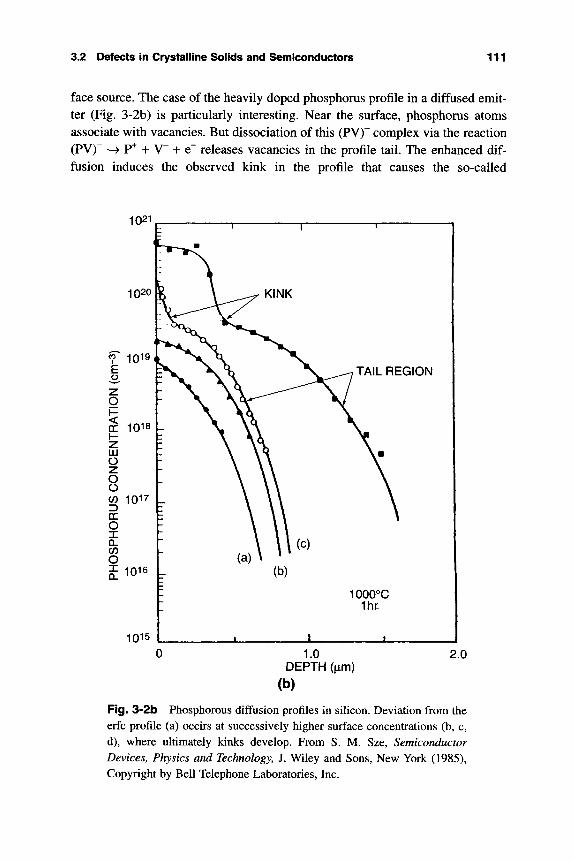
3.2 Defects in Crystalline Solids and Semiconductors 111
face source. The case of the heavily doped phosphorus profile in a diffused emit-ter (Fig. 3-2b) is particularly interesting. Near the surface, phosphorus atoms associate with vacancies. But dissociation of this (PV)~ complex via the reaction (PV)" —> P" + V~ + e~ releases vacancies in the profile tail. The enhanced dif-fusion induces the observed kink in the profile that causes the so-called
1021
TAIL REGION
1015
1000°C Ihr-
X 1.0
DEPTH (jim) (b)
2.0
Fig. 3-2b Phosphorous diffusion profiles in silicon. Deviation from the erfc profile (a) occirs at successively higher surface concentrations (b, c, d), where ultimately kinks develop. From S. M. Sze, Semiconductor Devices, Physics and Technology, J. Wiley and Sons, New York (1985), Copyright by Bell Telephone Laboratories, Inc.
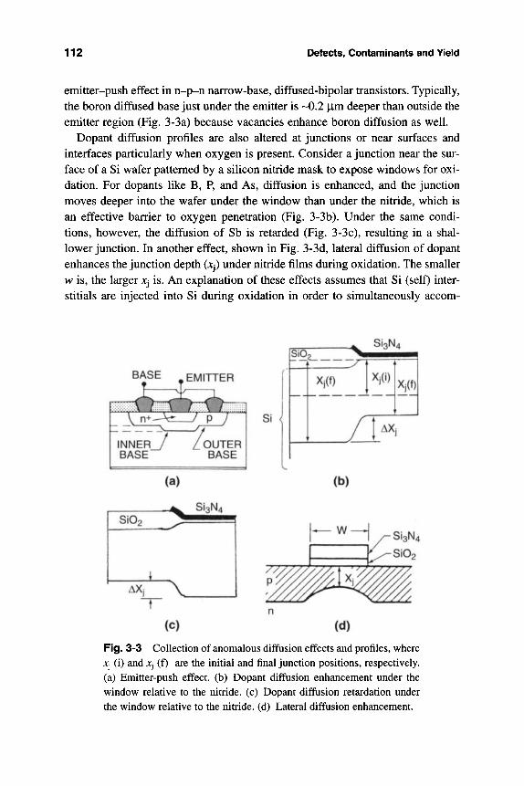
112 Defects, Contaminants and Yield
emitter-push effect in n-p-n narrow-base, diffused-bipolar transistors. Typically, the boron diffused base just under the emitter is -0.2 |im deeper than outside the emitter region (Fig. 3-3a) because vacancies enhance boron diffusion as well.
Dopant diffusion profiles are also altered at junctions or near surfaces and interfaces particularly when oxygen is present. Consider a junction near the sur-face of a Si wafer patterned by a silicon nitride mask to expose windows for oxi-dation. For dopants like B, P, and As, diffusion is enhanced, and the junction moves deeper into the wafer under the window than under the nitride, which is an effective barrier to oxygen penetration (Fig. 3-3b). Under the same condi-tions, however, the diffusion of Sb is retarded (Fig. 3-3c), resulting in a shal-lower junction. In another effect, shown in Fig. 3-3d, lateral diffusion of dopant enhances the junction depth (jCj) under nitride films during oxidation. The smaller w is, the larger jCj is. An explanation of these effects assumes that Si (self) inter-stitials are injected into Si during oxidation in order to simultaneously accom-
BASE .EMITTER
SiO • "
'
2 3! J^
m
/
Si3N4
Xj(i)
' i
1 AX *
Xj(f)
'
j
Fig. 3-3 Collection of anomalous diffusion effects and profiles, where JCj (i) and Xj (f) are the initial and final junction positions, respectively, (a) Emitter-push effect, (b) Dopant diffusion enhancement under the window relative to the nitride, (c) Dopant diffusion retardation under the window relative to the nitride, (d) Lateral diffusion enhancement.
3.2 Defects in Crystalline Solids and Semiconductors 113
modate the volume expansion stemming from oxide formation and reduce the interfacial stress that is generated. Semiconductor point defects include intersti-tials, and like vacancies, they may occur in nonequilibrium concentrations. Dopants (B and P) that prefer to use interstitials to facilitate mass transport show oxidation-enhanced diffusion, while the opposite is true for Sb, which diffuses via a vacancy mechanism.
Calling these enhancements and retardations of dopant concentration process-ing defects is perhaps too strong an attribution. Even though they alter intended device behavior, their effects can be designed against in most cases.
3.2.2.2 Oxygen in Crystalline Silicon It was the fate of sihcon, alu-minum, and oxygen, the most abundant elements on earth, to be brought together in the minutest of amounts to make integrated circuits possible. While these elements play unambiguously beneficial roles in semiconductor, conductor, and insulator functions, the presence of oxygen within silicon is like a "two-edged sword" (4) as far as device behavior is concerned. Oxygen enters CZ grown crystals because the melt continually erodes and dissolves the Si02 cru-cible wall during crystal pulling. A snapshot of the way defects enter the pulled crystal is schematically conveyed in Fig. 3-4. Point defects present in solid solu-tion at the highest temperatures promote the nucleation and growth of disloca-tion defects and oxide precipitates as the crystal cools. Within crystalline Si, oxygen reveals its many-faceted behavior depending on temperature. When dis-solved, oxygen occupies an interstitial site and is electrically inactive. Upon heating silicon to various temperature ranges, the changes that occur are sum-marized in Table 3-2. When oxygen-induced defects are retained in wafers at room temperature, they can be a source of considerable concern.
3.2.2.3 Gettering Treatments that remove process-induced contaminants from the active regions of the Si wafer, where devices are being fabricated, are known as gettering (5). Metal contaminants are the particular targets of gettering processes because they, in combination with precipitates at dislocations and stacking faults, cause excessive leakage currents and low junction-breakdown voltages. There are two types of gettering:
a. Extrinsic (or external). In this case gettering is achieved by deliberately introducing trapping sites in the back side of the Si wafer. Through surface dam-age produced by mechanical abrasion, ion implantation or laser beam heating and cooling, dislocations are generated. At high temperatures (~1000°C) these defects attract harmful metals such as Cu, Fe, Ni, and Cr, which diffuse to them from the active device regions. The kinetics of gettering depend on the rates of impurity release from the associated state, diffusion to, and capture by the getter site.
114 Defects, Contaminants and Yield
400°C
700°C
800°C
900°C
1000°C
1100°C
Interstitial oxygen forms donor complex
Homogeneous nucleation of oxide
Growth of oxide precipitates
Nucleation of oxide precipitates on stacking faults and dislocation loops
Condensation of interstitials to form stacking faults and dislocation loops
Oxygen, carbon and interstitials dissolved in solution
o SI
DISLOC LOOP
0.0 0*0
STACKING FAULtj
^ " f l f l t l " ^ ^
Fig. 3-4 Defect interactions and precipitation reactions in CZ grown silicon single crystals as a function of temperature.
b. Intrinsic (or internal). Intrinsic gettering is employed to remove both harmful oxygen and metallic elements through heat treatment alone. First, wafers should ideally contain an oxygen concentration of about 8.5 x 10 ^ cm~ . After an elevated temperature solution heat treatment the wafers are cooled, and oxygen precipitates from solid solution in the form of Si02 particles. These plas-tically compress the lattice, locally generating dislocations and stacking faults that tie up impurities in the manner described above for extrinsic gettering. In bipolar and CMOS technologies, which require higher process temperatures and a larger number of processing steps compared to conventional NMOS technol-ogy, attention must be paid to the problem of wafer warpage during thermal treatments (6).
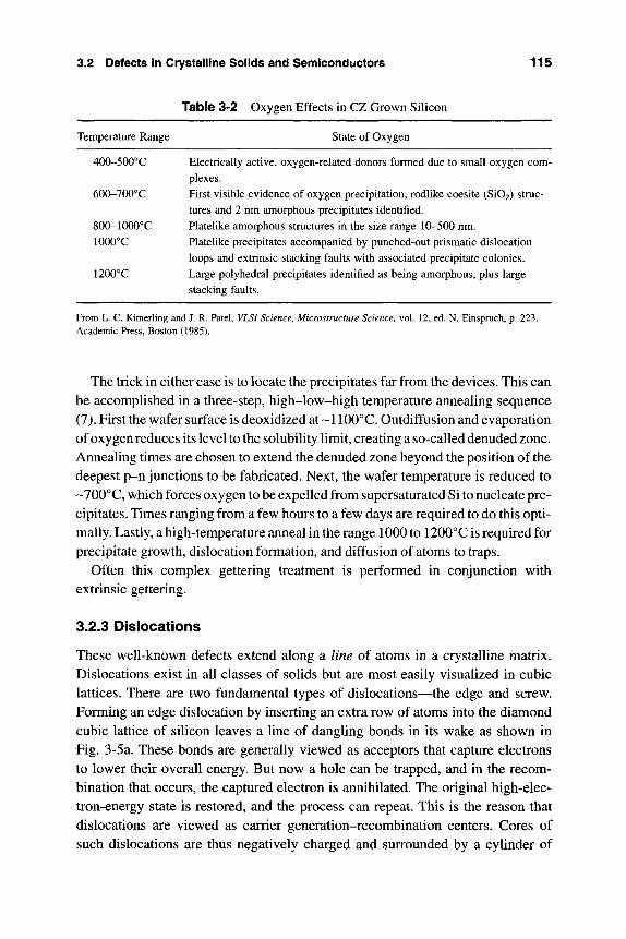
3.2 Defects in Crystalline Solids and Semiconductors 115
Table 3-2 Oxygen Effects in CZ Grown Silicon
Temperature Range State of Oxygen
400-500°C Electrically active, oxygen-related donors formed due to small oxygen com-plexes.
600-700°C First visible evidence of oxygen precipitation, rodlike coesite (Si02) struc-tures and 2 nm amorphous precipitates identified.
800-1000°C Platelike amorphous structures in the size range 10-500 nm. 1000°C Platelike precipitates accompanied by punched-out prismatic dislocation
loops and extrinsic stacking faults with associated precipitate colonies. 1200°C Large polyhedral precipitates identified as being amorphous, plus large
stacking faults.
From L. C. Kimerling and J. R. Patel, VLSI Science, Microstructure Science, vol. 12, ed. N. Einspruch, p. 223, Academic Press, Boston (1985).
The trick in either case is to locate the precipitates far from the devices. This can be accomplished in a three-step, high-low-high temperature annealing sequence (7). First the wafer surface is deoxidized at ~1100°C. Outdiffusion and evaporation of oxygen reduces its level to the solubility limit, creating a so-called denuded zone. Annealing times are chosen to extend the denuded zone beyond the position of the deepest p-n junctions to be fabricated. Next, the wafer temperature is reduced to ~700°C, which forces oxygen to be expelled from supersaturated Si to nucleate pre-cipitates. Times ranging from a few hours to a few days are required to do this opti-mally. Lastly, a high-temperature anneal in the range 1000 to 1200°C is required for precipitate growth, dislocation formation, and diffusion of atoms to traps.
Often this complex gettering treatment is performed in conjunction with extrinsic gettering.
3.2.3 Dislocations
These well-known defects extend along a line of atoms in a crystalline matrix. Dislocations exist in all classes of solids but are most easily visualized in cubic lattices. There are two fundamental types of dislocations—the edge and screw. Forming an edge dislocation by inserting an extra row of atoms into the diamond cubic lattice of silicon leaves a line of dangling bonds in its wake as shown in Fig. 3-5a. These bonds are generally viewed as acceptors that capture electrons to lower their overall energy. But now a hole can be trapped, and in the recom-bination that occurs, the captured electron is annihilated. The original high-elec-tron-energy state is restored, and the process can repeat. This is the reason that dislocations are viewed as carrier generation-recombination centers. Gores of such dislocations are thus negatively charged and surrounded by a cylinder of
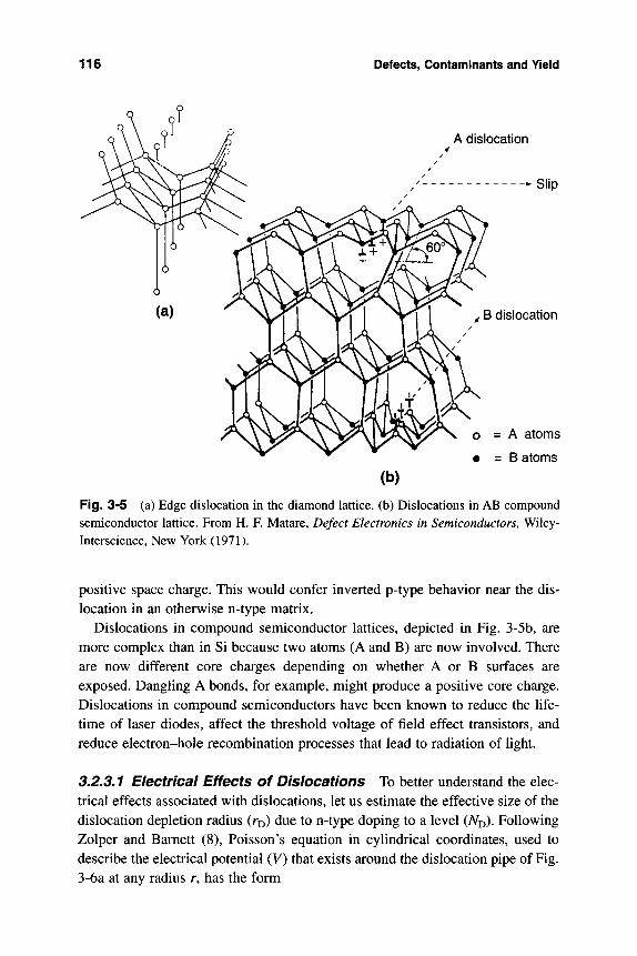
116 Defects, Contaminants and Yield
A dislocation
Slip
B dislocation
o = A atoms
• = B atoms
(b)
Fig. 3-5 (a) Edge dislocation in the diamond lattice, (b) Dislocations in AB compound semiconductor lattice. From H. F. Matare, Defect Electronics in Semiconductors, Wiley-Interscience, New York (1971).
positive space charge. This would confer inverted p-type behavior near the dis-location in an otherwise n-type matrix.
Dislocations in compound semiconductor lattices, depicted in Fig. 3-5b, are more complex than in Si because two atoms (A and B) are now involved. There are now different core charges depending on whether A or B surfaces are exposed. Dangling A bonds, for example, might produce a positive core charge. Dislocations in compound semiconductors have been known to reduce the life-time of laser diodes, affect the threshold voltage of field effect transistors, and reduce electron-hole recombination processes that lead to radiation of light.
3.2.3.1 Electrical Effects of Dislocations To better understand the elec-trical effects associated with dislocations, let us estimate the effective size of the dislocation depletion radius (r^) due to n-type doping to a level (A^D)- Following Zolper and Bamett (8), Poisson's equation in cylindrical coordinates, used to describe the electrical potential (V) that exists around the dislocation pipe of Fig. 3-6a at any radius r, has the form
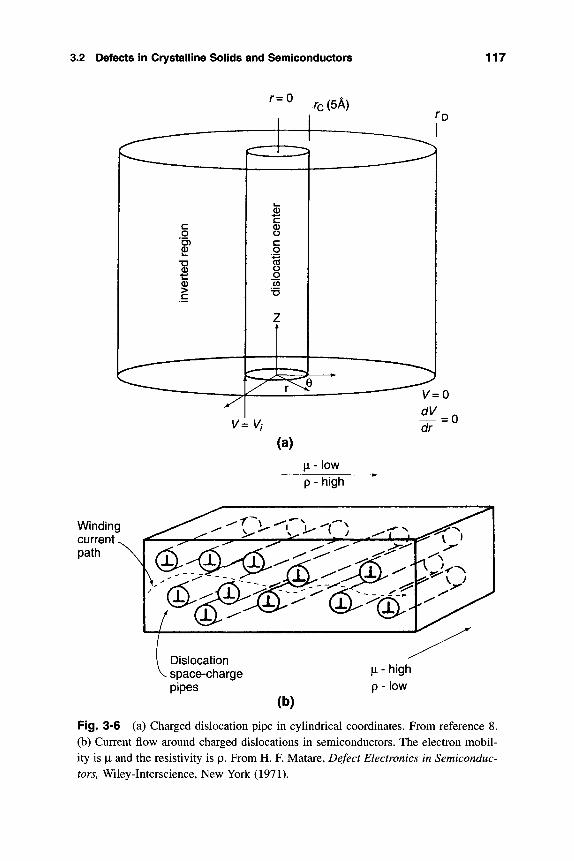
3.2 Defects in Crystalline Solids and Semiconductors 117
r=0
c g
>
0 +-C o o c o
GO T3
rc(5A)
^ ' ^ ^ ^ ^ ^
\ / = \ / ,
(a) |x- low
p - high
Winding current path
Dislocation . space-charge pipes
(b)
|Li - high p - low
Fig. 3-6 (a) Charged dislocation pipe in cylindrical coordinates. From reference 8. (b) Current flow around charged dislocations in semiconductors. The electron mobil-ity is \i and the resistivity is p. From H. F. Matare, Defect Electronics in Semiconduc-tors, Wiley-Interscience, New York (1971).
118 Defects, Contaminants and Yield
T^' (3-3)
Here p is the charge density, e is the electronic charge, while e and EQ are the dielectric constant and permittivity of free space, respectively. As boundary con-ditions, it is assumed that V (ro) = 0, and dV(rxy)ldr - 0. Upon double integration and substitution of these boundary conditions,
^ . . . . - . .'4-lnrir (3-4)
Finally, at the dislocation core radius (r^), typically 0.5 nm, a potential V^ exists that causes inversion. Assuming Vi at r^ (i.e., Vir^) = Vi) we can then solve for TD at any doping level by trial-and-error methods. Calculation shows that if Vi= IV, and A D = 2x10^^ cm~ , then ro = 44 nm. Physically, the dislocation core traps electrons and in the process is surrounded by a positively charged space-charge region.
The implications of charged dislocations on current flow are depicted in Fig. 3-6b. Tortuous current paths result in increased carrier scattering and reduced mobility. Anisotropy develops such that carrier mobility and conductivity normal to dislocation lines are both reduced relative to their behavior parallel to them. Dislocations have also long been identified as charge recombination centers that degrade the minority carrier diffusion length and lifetime. Table 3-3 indicates the extent to which dislocations degrade the efficiency of silicon ribbon solar cells. Perhaps more significant than the effect of dislocations on carrier motion is their ability to interact with assorted local impurities and point defects. When metal-lic impurities segregate at dislocations, problems due to excessive leakage cur-rents and shorting of junctions arise. We have already noted such interactions in the practice of gettering metallic impurities by intentionally introducing disloca-tions.
Table 3-3 Correlation Between Dislocation Density and Solar Cell Characteristics
Dislocation Density (cm"^) Minority Carrier Diffusion Length (|im) Cell Efficiency %
Region At twins Bulk 2 X 10^ -10^ 12 9.5 3 X 10^ -10^ 19 10.0 {None observed} 135 14.3 {None observed} 156 14.9
After S. Mahajan, Progress in Materials Science 33, 1 (1989).
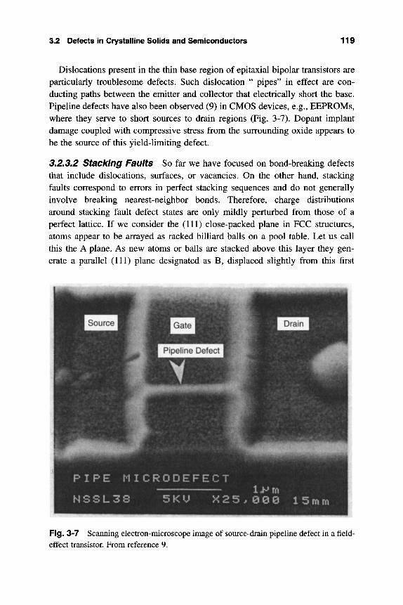
3.2 Defects in Crystalline Solids and Semiconductors 119
Dislocations present in the thin base region of epitaxial bipolar transistors are particularly troublesome defects. Such dislocation " pipes" in effect are con-ducting paths between the emitter and collector that electrically short the base. Pipeline defects have also been observed (9) in CMOS devices, e.g., EEPROMs, where they serve to short sources to drain regions (Fig. 3-7). Dopant implant damage coupled with compressive stress from the surrounding oxide appears to be the source of this yield-limiting defect.
3.2.3.2 StQCking Faults So far we have focused on bond-breaking defects that include dislocations, surfaces, or vacancies. On the other hand, stacking faults correspond to errors in perfect stacking sequences and do not generally involve breaking nearest-neighbor bonds. Therefore, charge distributions around stacking fault defect states are only mildly perturbed from those of a perfect lattice. If we consider the (111) close-packed plane in FCC structures, atoms appear to be arrayed as racked billiard balls on a pool table. Let us call this the A plane. As new atoms or balls are stacked above this layer they gen-erate a parallel (111) plane designated as B, displaced slightly from this first
Fig. 3-7 ScanniTig electron-microscope image of source-drain pipeline defect in a field-effect transistor. From reference 9.
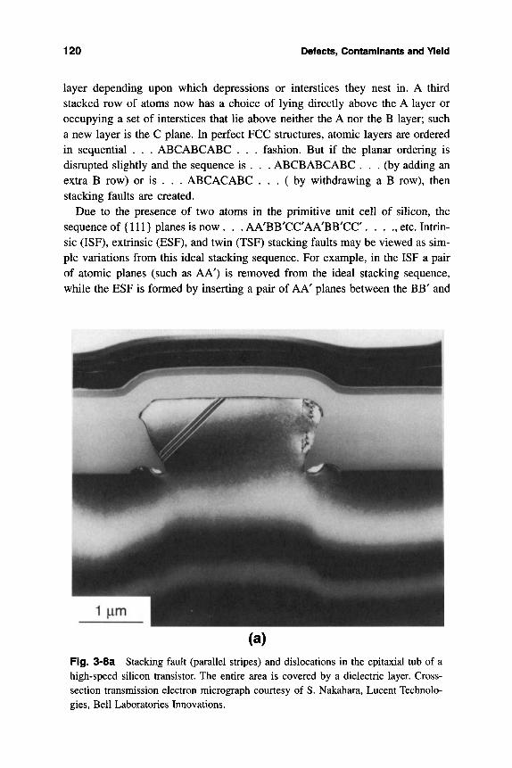
120 Defects, Contaminants and Yield
layer depending upon which depressions or interstices they nest in. A third stacked row of atoms now has a choice of lying directly above the A layer or occupying a set of interstices that lie above neither the A nor the B layer; such a new layer is the C plane. In perfect FCC structures, atomic layers are ordered in sequential . . . ABCABCABC . . . fashion. But if the planar ordering is disrupted slightly and the sequence is . . . ABCBABCABC . . . (by adding an extra B row) or is . . . ABCACABC . . . ( by withdrawing a B row), then stacking faults are created.
Due to the presence of two atoms in the primitive unit cell of silicon, the sequenceof{ 111} planes is now. . . AA'BB'CC'AA'BB'CC . . . ., etc. Intrin-sic (ISF), extrinsic (ESF), and twin (TSF) stacking faults may be viewed as sim-ple variations from this ideal stacking sequence. For example, in the ISF a pair of atomic planes (such as AA') is removed from the ideal stacking sequence, while the ESF is formed by inserting a pair of AA' planes between the BB' and
Fig. 3-8a Stacking fault (parallel stripes) and dislocations in the epitaxial tub of a high-speed silicon transistor. The entire area is covered by a dielectric layer. Cross-section transmission electron micrograph courtesy of S. Nakahara, Lucent Technolo-gies, Bell Laboratories Innovations.
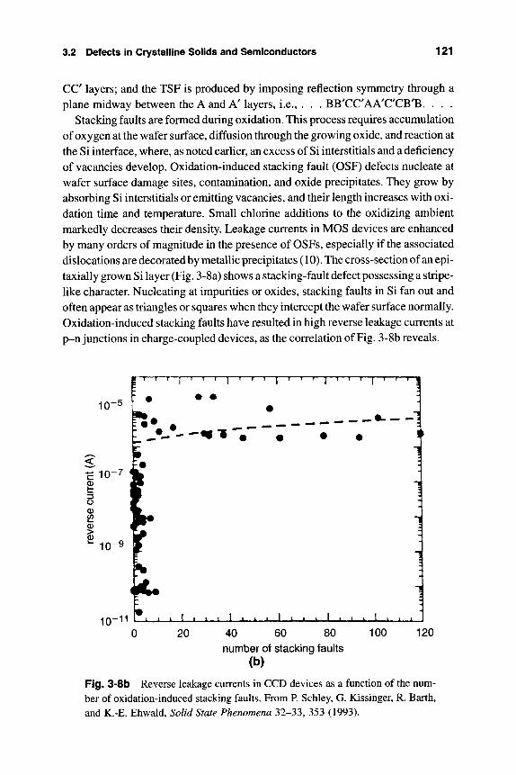
3.2 Defects in Crystalline Solids and Semiconductors 121
CC layers; and the TSF is produced by imposing reflection symmetry through a plane midway between the A and A' layers, i.e., . . . BB'CC'AA'C'CB'B. . . .
Stacking faults are formed during oxidation. This process requires accumulation of oxygen at the wafer surface, diffusion through the growing oxide, and reaction at the Si interface, where, as noted earlier, an excess of Si interstitials and a deficiency of vacancies develop. Oxidation-induced stacking fault (OSF) defects nucleate at wafer surface damage sites, contamination, and oxide precipitates. They grow by absorbing Si interstitials or emitting vacancies, and their length increases with oxi-dation time and temperature. Small chlorine additions to the oxidizing ambient markedly decreases their density. Leakage currents in MOS devices are enhanced by many orders of magnitude in the presence of OSFs, especially if the associated dislocations are decorated by metallic precipitates (10). The cross-section of an epi-taxially grown Si layer (Fig. 3-8a) shows a stacking-fault defect possessing a stripe-like character. Nucleating at impurities or oxides, stacking faults in Si fan out and often appear as triangles or squares when they intercept the wafer surface normally. Oxidation-induced stacking faults have resulted in high reverse leakage currents at p-n junctions in charge-coupled devices, as the correlation of Fig. 3-8b reveals.
0 20 40 60 80 100 120 number of stacking faults
(b)
Fig. 3-8b Reverse leakage currents in CCD devices as a function of the num-ber of oxidation-induced stacking faults. From P. Schley, G. Kissinger, R. Earth, and K.-E. Ehwald, Solid State Phenomena 32-33, 353 (1993).
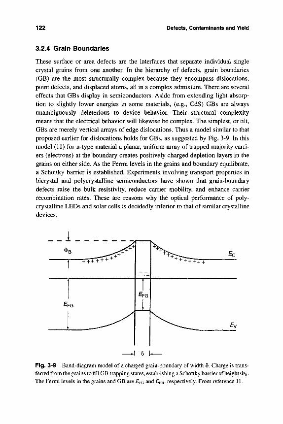
122 Defects, Contaminants and Yield
3.2.4 Grain Boundaries
These surface or area defects are the interfaces that separate individual single crystal grains from one another. In the hierarchy of defects, grain boundaries (GB) are the most structurally complex because they encompass dislocations, point defects, and displaced atoms, all in a complex admixture. There are several effects that GBs display in semiconductors. Aside from extending light absorp-tion to slightly lower energies in some materials, (e.g., CdS) GBs are always unambiguously deleterious to device behavior. Their structural complexity means that the electrical behavior will likewise be complex. The simplest, or tilt, GBs are merely vertical arrays of edge dislocations. Thus a model similar to that proposed earlier for dislocations holds for GBs, as suggested by Fig. 3-9. In this model (11) for n-type material a planar, uniform array of trapped majority carri-ers (electrons) at the boundary creates positively charged depletion layers in the grains on either side. As the Fermi levels in the grains and boundary equilibrate, a Schottky barrier is established. Experiments involving transport properties in bicrystal and polycrystalline semiconductors have shown that grain-boundary defects raise the bulk resistivity, reduce carrier mobility, and enhance carrier recombination rates. These are reasons why the optical performance of poly-crystalline LEDs and solar cells is decidedly inferior to that of similar crystalline devices.
^ B
1"
E
'
- - ^ "T++++^
1
t I
N*^TT- ^c + I+T+-++ -
^v
1 8 k-
Fig. 3-9 Band-diagram model of a charged grain-boundary of width 6. Charge is trans-ferred from the grains to fill GB trapping states, establishing a Schottky barrier of height OB. The Fermi levels in the grains and GB are £ FG and Ep^, respectively. From reference 11.
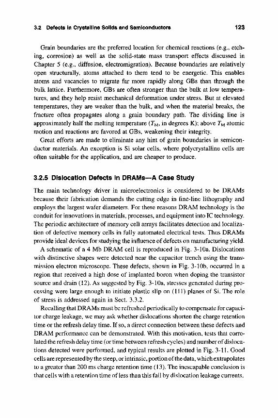
3.2 Defects in Crystalline Solids and Semiconductors 123
Grain boundaries are the preferred location for chemical reactions (e.g., etch-ing, corrosion) as well as the solid-state mass transport effects discussed in Chapter 5 (e.g., diffusion, electromigration). Because boundaries are relatively open structurally, atoms attached to them tend to be energetic. This enables atoms and vacancies to migrate far more rapidly along GBs than through the bulk lattice. Furthermore, GBs are often stronger than the bulk at low tempera-tures, and they help resist mechanical deformation under stress. But at elevated temperatures, they are weaker than the bulk, and when the material breaks, the fracture often propagates along a grain boundary path. The dividing line is approximately half the melting temperature (Tu, in degrees K); above TM atomic motion and reactions are favored at GBs, weakening their integrity.
Great efforts are made to eliminate any hint of grain boundaries in semicon-ductor materials. An exception is Si solar cells, where polycrystalline cells are often suitable for the application, and are cheaper to produce.
3.2.5 Dislocation Defects In DRAMs—A Case Study
The main technology driver in microelectronics is considered to be DRAMs because their fabrication demands the cutting edge in JSne-line lithography and employs the largest wafer diameters. For these reasons DRAM technology is the conduit for innovations in materials, processes, and equipment into IC technology. The periodic architecture of memory cell arrays facilitates detection and localiza-tion of defective memory cells in fully automated electrical tests. Thus DRAMs provide ideal devices for studying the influence of defects on manufacturing yield.
A schematic of a 4 Mb DRAM cell is reproduced in Fig. 3-10a. Dislocations with distinctive shapes were detected near the capacitor trench using the trans-mission electron microscope. These defects, shown in Fig. 3-lOb, occurred in a region that received a high dose of implanted boron when doping the transistor source and drain (12). As suggested by Fig. 3-lOa, stresses generated during pro-cessing were large enough to initiate plastic slip on (111) planes of Si, The role of stress is addressed again in Sect. 3.3.2.
Recalling that DRAMs must be refreshed periodically to compensate for capaci-tor charge leakage, we may ask whether dislocations shorten the charge retention time or the refresh delay time. If so, a direct connection between these defects and DRAM performance can be demonstrated. With this motivation, tests that corre-lated the refresh delay time (or time between refresh cycles) and number of disloca-tions detected were performed, and typical results are plotted in Fig. 3-11. Good cells are represented by the steep, or intrinsic, portion of the data, which extrapolates to a greater than 200 ms charge retention time (13). The inescapable conclusion is that cells with a retention time of less than this fail by dislocation leakage currents.
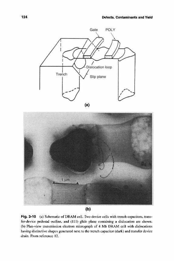
124 Defects, Contaminants and Yield
Gate POLY
(b)
Fig. 3-10 (a) Schematic of DRAM cell. Two device cells with trench capacitors, trans-fer-device pedestal outline, and (111) glide plane containing a dislocation are shown, (b) Plan-view transmission electron micrograph of 4 Mb DRAM cell with dislocations having distinctive shapes generated next to the trench capacitor (dark) and transfer device drain. From reference 12.
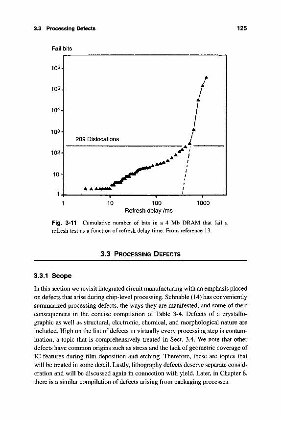
3.3 Processing Defects 125
Fail bits
106-
105,
104.
103-
102-
10-
1 .
209 Dislocations
1
J 1 1
f
/ /
/
1 "' '*
10 100 Refresh delay /ms
1000
Fig. 3-11 Cumulative number of bits in a 4 Mb DRAM that fail a refresh test as a function of refresh delay time. From reference 13.
3.3 PROCESSING DEFECTS
3.3.1 Scope
In this section we revisit integrated circuit manufacturing with an emphasis placed on defects that arise during chip-level processing. Schnable (14) has conveniently summarized processing defects, the ways they are manifested, and some of their consequences in the concise compilation of Table 3-4. Defects of a crystallo-graphic as well as structural, electronic, chemical, and morphological nature are included. High on the list of defects in virtually every processing step is contam-ination, a topic that is comprehensively treated in Sect. 3.4. We note that other defects have common origins such as stress and the lack of geometric coverage of IC features during film deposition and etching. Therefore, these are topics that will be treated in some detail. Lastly, lithography defects deserve separate consid-eration and will be discussed again in connection with yield. Later, in Chapter 8, there is a similar compilation of defects arising from packaging processes.

126 Defects, Contaminants and Yield
Table 3-4 Defects Associated with Microelectronics Manufacturing Processes
at the Chip Level
1. Epitaxy Defects Contamination; Excessive lateral autodoping; Excessive vertical autodop-ing; Film too thick or too thin; Haze; Heavy metal contamination; Hillocks; Inadequate resistivity uniformity; Inadequate thickness uniformity; Low minority carrier hfetime; Poor crystallographic quality; Pattern shift; Resistivity too high; Roughness; Scratches; Stacking Faults.
2. Oxidation Defects Alkali ion contamination; Dopant penetration through oxide mask; Excessive dopant pile-up; Fixed oxide charge incorrect; Heavy metal contamination; Inadequate radiation hardness; Interface state density too high; Localized oxide thinning; Oxidation-induced stacking faults; Oxide too thick or too thin; Oxide trapped charge too high; Particulate contami-nation; Shp in substrate; Slow trapping instability; Thickness nonuniform; White ring (Kool effect).
3. Fhotoreslst Patterning Defects Alkali ion contamination; Bridging; Inadequate planariza-tion; Inadequate resist adhesion; Inadequate resist etch resistance; Inadequate resolution; Inade-quate step coverage; Incorrect edge contour; Incorrect linewidth; Intrusions; Misalignment; Missing images; Mousebites; Neckdowns; Notching; Opaque spots; Overexposure; Particulate contamina-tion; Pattern discontinuities; Pattern distortion; Pinholes; Poor resist etch resistance; Poor resist thickness uniformity; Protrusions; Resist too thick or too thin; Rough edges; Rounding; Scratches; Scunmiing; Spacing violations; Underexposure.
4. Diffusion Alkali contamination; Bandgap narrowing; Boron penetration through oxide; Crys-tallographic damage; Diffusion pipes; Dislocations; Dopant precipitation; Emitter push; Heavy metal contamination; Inadequate uniformity; Laterally enhanced diffusion; Liquid-phase penetra-tion of oxide mask; Popcorn noise; Sheet resistivity too high; Sheet resistivity too low; Slip; Junc-tions too deep or too shallow.
5. Ion Implantation Charge buildup; Contaminants in implant beam; Inadequate dose unifor-mity; Incorrect depth; Incorrect dopant species; Incorrect dose; Incorrect implant angle; Metallic contamination; Neutral species in implant beam; Overheating; Particulate contamination; Penetra-tion into underlying device; Semiconductor lattice damage.
t 6. Thermal'Treatment Alkali ion contamination; Carbon contaminatioil; Heavy metal contami-nation; Incorrect ambient; Incorrect cooling or heating rate; Incorrect temperature; Incorrect time; Particulate contamination; Slip; Thermal pitting.
7. Cleaning Alkali ion contamination; Excessive etching; Heavy; metal contaminationv Incom-plete contaminant removal; Particulate contamination; Pitting; Radiation damage; Scratches; Sili-con crystallographic damage.
8. Wet Chemical Etching Alkali ion contamination; Corrosive residue; Freckles (unetched precipitates); Heavy metal contamination; Insoluble residue; Local cell etching; Loss of resist adhesion; Nonuniform etching; Overetching; Particulate contamination; Photomask erosion; Photo-voltage effects; Pitting; Poor etch ratio; Poor wetting; Staining; Undercutting; Underetching; Wrong etch rate.
3.3 Processing Defects 127
Table 3-4 continued
9. Plasma Etching Charge buildup; Corrosive residues; Excessive etching of substrate; Exces-sive loading effects; Excessive resist erosion; Excessive variation in induction time; Freckles (unetched precipitates); Grass; Hydrogen donor effects in Si; Inadequate etch ratios; Incorrect edge angle; Insufficient amount of etching; Ionic contamination; Low selectivity; Metallic contamina-tion; Nonuniform etching; Overetching; Poor etching uniformity; Radiation damage; Radiation damage to Si02; Residue in etched openings; Residue on sidewalls; Silicon crystal damage; Stringers; Undercutting; Underetchin^.
10i Cliemicaf Vapor Deposition Devitrification; Etch rate too high; Excessive compressive stress; Excessive hydrogen content; Excessive tensile stress; Excessively hydroscopic; Insufficient conformality; Localized etch rate at step too high; Nonuniform thickness; Not stoichiometric; Too thick or too thin; Wrong composition.
11. Metallization Black gold; Contains voids; Ductility too low; Excessive native oxide in con-tacts; Excessive oxide content in metal; Excessive oxygen in initially deposited region; Excessive roughness; High sheet resistivity; Hillocks; In-process radiation damage; Low resistivity ratio; Microcracks; Poor adhesion; Poor step coverage; Poor thickness uniformity; Susceptible to corro-sion; Susceptible to electromigration; Too thick or thin; Wrong alloy composition.
From G.L. Schnable in Microelectronics Manufacturing Diagnostics Handbook, ed. A. H. Landsberg, Van Nos-trand Reinhold, New York (1993).
3.3.2 Stress and Defects
Stress in IC chips is not viewed as a defect per se, because it is an intrinsic conse-quence of processing dissimilar materials in contact. Nevertheless, stress has an important influence in generating or exacerbating many Table 3-4 defects such as hillocks, stacking faults, slip, internal stress, microcracking, and corrosion. In process steps involving film growth (oxidation) or film deposition (CVD, metal-lization), internal stresses develop in the bilayer film-substrate structurei
Internal stresses arise in various manufacturing operations. When a homoge-neous metal strip is reduced slightly by rolling, the surface fibers are extended more than the interior bulk. The latter resists the fiber extension and places the surfacein compression, while the interior is stressed in tension. This residual stress distribu-tion is locked into the metal but can be released like a jack-in-the-box. Simply machining a thin surface layer from the rolled metal surface will upset the mechan-ical equilibrium and cause the remaining material to bow. Residual stresses also arise in castings, heat-treated glass, and machined and ground materials.
A more pertinent example of residual stress occurs in silicon wafers whose back sides are thinned by grinding prior to dicing (15). Thinner wafers facilitate dicing, dissipate h ^ ^ better, and inake for thinner packages. Unfortunately, grinding
128 Defects, Contaminants and Yield
induces stresses that cause wafers to warp and more easily break during the dic-ing process. Furthermore, warped dies are more difficult to electrically contact and mount in the package. All in all, yield can suffer appreciably due to warped wafers. This underscores the importance of understanding and controlling stress.
3.3.2.1 Internal Stress We all know that stresses and strains will develop throughout a body when forces are applied to it. Under elastic loading condi-tions, the stresses and strains disappear upon unloading. But materials that are plastically deformed or heated may sometimes contain residual stresses even when the plastic load or heat is removed. Furthermore, what are we to make of processed wafers that are internally stressed even though no mechanical forces were ever applied to them? Such situations arise all too frequently in thin films attached to substrates, and in these cases internal or residual stresses are said to exist. Internal stresses have important implications in influencing product yield as well as subsequent reliability. There are two main sources of internal stress, and each will be discussed in turn.
3.3.2.2 Extrinsic Residual Stress These stresses, commonly called ther-mal stresses, originate from the thermal expansion or contraction of materials when they are mechanically constrained. To see how thermal stress can develop in a homogeneous body, consider a rod of length LQ clamped at both ends. If its temperature is raised from T^ to T, the rod would tend to expand in length by an amount equal to a (T - T^) L^, where a is the coefficient of thermal expansion (CTE) defined by a = AL/L^iT - T^) (fT^). But the rod is constrained and is, therefore, effectively shortened in compression. The compressive strain is sim-ply ^ = A LJLo = -a(T- To) Lo/Lo or - a (T - To). By Hooke's law a stress a develops that is given by Ee, where E is the modulus of elasticity. Therefore, combining terms (neglecting signs) yields
c = Ea(T-To). (3-5)
Processing of IC chips generally involves bi- and multilayers of different mate-rials, and a number of failure and reliability problems discussed in this book can be attributed to internal or residual stresses in such structures. Even the outwardly homogeneous ground silicon wafer discussed above is an effective bilayer con-sisting of a thin stressed surface layer and the contiguous bulk with a stress of opposite sign. Internal stresses invariably develop in film/substrate combinations because of thermal mismatch between the film and substrate at the film formation and use temperatures. To see why, we assume that the film is stress free at the ele-vated deposition temperature T, and that oCf > a^. As the film cools to room tem-perature To, it contracts more than the substrate, as shown in Fig. 3-12a. Regard-

3.3 Processing Defects 129
less of the resultant stress distribution that prevails, the structure must be in mechanical equilibrium. This requires that both the net force (F) and bending moment (M) vanish on every film/substrate free body cross section. Thus
F = jodA = 0 (3-6)
and
M = jay dA = 0, (3-7)
where A is the sectional area and y is the moment arm. Compatibility demands that both the film and substrate have the same length. A compromise is struck, and the film stretches while the substrate contracts by an equal amount to keep the overall length identical in each.
However, the combination is still not in mechanical equilibrium because there is still an unbalanced end moment. To compensate, the film/substrate pair elasti-cally bends as shown if not restrained from moving. Thus, films containing inter-nal tensile stresses bend the substrate concave upward. In an entirely analogous fashion, compressive stresses develop in films that tend to thermally contract less than the substrate. Internal compressive film stresses, therefore, now bow the substrate convex downward (Fig. 3-12b). These results are perfectly general
FILM m SUBSTRATE SUBSTRATE
FILM UNDER RESIDUAL FILM UNDER RESIDUAL TENSILE STRESS COMPRESSIVE STRESS
(a) (b)
Fig. 3-12 (a) Development of residual tensile stress in a film when oCf > ttg. (b) Development of residual compressive stress in a film when oCf < a^. From reference 16.
130 Defects, Contaminants and Yield
regardless of the specific mechanisms that cause films to stretch or shrink rela-tive to substrates. Sometimes, the tensile stresses are sufficiently large to cause film fracture. Similarly, excessively high compressive stresses can cause film wrinkling and local loss of adhesion to the substrate. Examples of both effects are shown in Fig. 3-13.
The magnitude of the thermal stress developed in the film is given by (16)
a = 1 - Vf [otf-aj(r-ro). (3-8)
where Vf is the Poisson ratio of the film. Stresses of lower magnitude and opposite sign develop in the substrate. It should be noted that across a film/substrate couple the strains are continuous, but there is no such restriction on the stresses. Because the elastic moduli of film and substrate differ, there is a stress discontinuity at the interface. Since two or more materials bonded to each other are involved in many
Fig. 3-13 Stresses in thin films that lead to fracture, (a) Image of tensile cracks in a chromium film electrodeposited on a nickel substrate that was subsequently pulled in tension.
3.3 Processing Defects 131
(b)
Fig. 3-13 (b) Optical micrograph of crazes in a tungsten thin film sputtered on a silicon substrate. Isotropic, compressive residual stresses with magnitudes of -1 to 3 GPa led to worm-like, wavy, and straight crack traces. Width of straight cracks is ~ 60|j.m. Courtesy of I.C, Noyan, IBM Corp,
applications, Eq. 3-8 is an important formula that is frequently quoted in the relia-bility literature. The right-hand side of this equation appears as a factor in virtually every thermal stress formula developed in connection with packaging and thermal cycling of IC chips during processing and use (see Chapter 8).
3,3.2,3 Intrinsic Residual Stress In addition to thermally induced stresses, there are intrinsic sources of stress that are operative at any given tem-perature. In films these stresses stem from growth processes, i.e., during epitaxy and structural evolution. Tensile stresses usually arise in metal and silicide films from densification phenomena arising from coalescence of nuclei, recrystalliza-tion, and grain growth. In each case the film shrinks relative to the substrate. On the other hand, hydration and ion implantation lead to compressive stress because they expand the film relative to the substrate.
132 Defects, Contaminants and Yield
There are complex reasons for the development of intrinsic residual strains, but in epitaxial films they include differences in lattice constant or lattice misfit between film and substrate. In producing high-quality epitaxial films of com-pound semiconductors it is critical that the lattice constants of the film (flf) and substrate (a^) be as closely matched as possible. Lattice mismatch or misfit ( / ) is defined as
/ = (3-9)
which is the negative of the elastic strain, e^, required to make the film register perfectly or epitaxially with the substrate. What happens during epitaxy is schematically indicated in Fig. 3-14. When/is zero there is perfect homoepitaxy and no strain or stress. For small values of/, straining of interfacial film-substrate atomic bonds is not sufficient to nucleate dislocations, and the interface is defect-free. However, for larger misfits the only way to reduce accumulated bond strain-energy is to generate undesirable misfit dislocations at the interface. For devices not to display degraded electrical behavior, misfit values less than 0.001 are pre-
HOMOEPITAXY HETEROEPITAXY-
FILM/SUBSTRATE
FILM
SUBSTRATE
MATCHED STRAINED RELAXED
Fig. 3-14 Schematic illustration of lattice matched, strained and relaxed heteroepi-taxial structures.
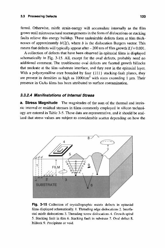
3.3 Processing Defects 133
ferred. Otherwise, misfit strain-energy will accumulate internally as the film grows until microstructural rearrangements in the form of dislocations or stacking faults relieve this energy buildup. These undesirable defects form at film thick-nesses of approximately bl{2f), where b is the dislocation Burgers vector. This means that defects will typically appear after ~ 200 nm of film growth if/= 0.001.
A collection of defects that have been observed in epitaxial films is displayed schematically in Fig. 3-15. All, except for the oval defects, probably need no additional comment. The troublesome oval defects are faceted growth hillocks that nucleate at the film-substrate interface, and they nest in the epitaxial layer. With a polycrystalline core bounded by four {111} stacking-fault planes, they are present in densities as high as 1000/cm^ with sizes exceeding 1 \\m. Their presence in GaAs films has been attributed to surface contamination.
3.3.2A Manifestations of Internai Stress
a. Stress Magnitude The magnitudes of the sum of the thermal and intrin-sic internal or residual stresses in films commonly employed in silicon technol-ogy are entered in Table 3-5. These data are representative, and it should be real-ized that stress values are subject to considerable scatter depending on how the
Fig. 3-15 Collection of crystallographic matrix defects in epitaxial films displayed schematically. 1. Threading edge dislocations 2. Interfa-cial misfit dislocations 3. Threading screw dislocations 4. Growth spiral 5. Stacking fault in film 6. Stacking fault in substrate 7. Oval defect 8. Hillock 9. Precipitate or void.
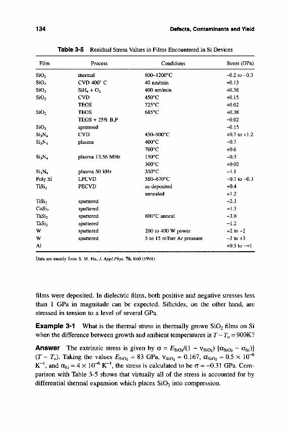
134 Defects, Contaminants and Yield
Table 3-5 Residual Stress Values in Films Encountered in Si Devices
Film
Si02 Si02 Si02 Si02
Si02
Si02 Si3N4 Si3N4
Si3N4
Si3N4 Poly Si
TiSi2
TiSi2 CoSi2 TaSi2 TaSi2 W W Al
Process
thermal CVD 400° C
SiH4 + 02 CVD TEOS TEOS TEOS + 25% B,P sputtered CVD plasma
plasma 13.56 MHz
plasma 50 kHz LPCVD PECVD
sputtered sputtered sputtered sputtered sputtered sputtered
Conditions
900-1200*'C 40 nm/min 400 nm/min 450°C 725°C 685°C
450-900**C 400°C / 700°C 150*'C 300°C 3 5 0 ^ 560-670°C as-deposited annealed
SOO' C anneal
200 to 400 W power 5 to 15 mTorr Ar pressure
Stress (GPa)
^2 to -0.3 +0.13 +0.38 +0.15 +0.02 +0.38
— 0 . 0 2 -0.15 +0.7 to+1.2 -0.7 +0.6 -0.3 +0.02 -1.1 -0.1 to-0.3 +0.4 +1.2 +2.3 +1.3 +3.0 +1.2 +2 to -2 -3 to +3 +0.5 to ~+l
Data are mostly from S. M. Hu, J. ApplPhys. 70, R60 (1991)
films were deposited. In dielectric films, both positive and negative stresses less than 1 GPa in magnitude can be expected. Silicides, on the other hand, are stressed in tension to a level of several GPa.
Example 3-1 What is the thermal stress in thermally grown Si02 films on Si when the difference between growth and ambient temperatures is 7 - T , = 900K?
Answer The extrinsic stress is given by a = £"8102/(1 ~ 3102) [0 5102 ~ ^si)] {T - To). Taking the values £5102 = 83 GPa, Vsioz = 0.167, asi02 = 0-5 x 10"^ K~\ and asi = 4 x 10"^ K"\ the stress is calculated to be a = -0.31 GPa. Com-parison with Table 3-5 shows that virtually all of the stress is accounted for by differential thermal expansion which places Si02 into compression.
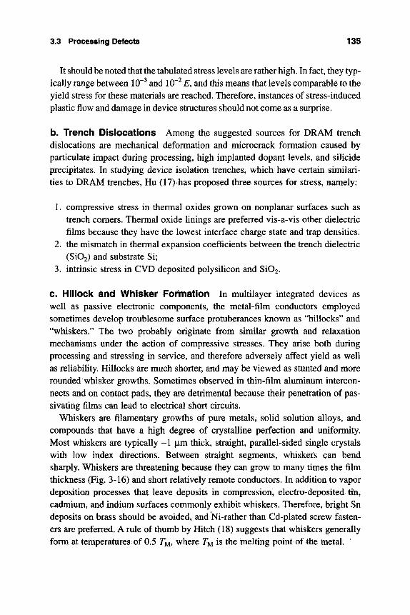
3.3 Processing Defects 135
It should be noted that the tabulated stress levels are rather high. In fact, they typ-ically range between 10" and 10" E, and this means that levels comparable to the yield stress for these materials are reached. Therefore, instances of stress-induced plastic flow and damage in device structures should not come as a surprise.
b. Trench Dislocations Among the suggested sources for DRAM trench dislocations are mechanical deformation and microcrack formation caused by particulate impact during processing, high implanted dopant levels, and silicide precipitates. M studying device isolation trenches, which have certain.similari-ties to DRAM trenches, Hu (17)rhas proposed three sources for stress, namely:
1. compressive stress in thermal oxides grown on nonplanar surfaces such as trench comers. Thermal oxide linings are preferred vis-a-vis other dielectric films because they have the lowest interface charge state and trap densities.
2. the mismatch in thermal expansion coefficients between the trench dielectric (Si02) and substrate Si;
3. intrinsic stress in CVD deposited poly silicon and Si02.
C. Hiiiocic and Wlliiker Formation In multilayer integrated devices as well as passive electronic components, the metal-film conductors employed sometimes develop troublesome surface protuberances known as "hillocks" and "whiskers." The two probably originate from similar growth and relaxation mechanisms under the action of compressive stresses. They arise both during processing and stressing in service, and therefore adversely affect yield as well as reliability. Hillocks are much shorter, and may be viewed as stunted and more rounded whisker growths. Sometimes observed in thin-film aluminum intercon-nects and on contact pads, they are detrimental because their penetration of pas-sivating films can lead to electrical short circuits.
Whiskers are filamentary growths of pure metals, solid solution alloys, and compounds that have a high degree of crystalline perfection and uniformity. Most whiskers are typically ~1 |im thick, straight, parallel-sided single crystals with low index directions. Between straight segments, whiskers can bend sharply. Whiskers are threatening because they can grow to many times the film thickness (Fig. 3-16) and short relatively remote conductors. In addition to vapor deposition processes that leave deposits in compression, electro-deposited tin, cadmium, and indium surfaces commonly exhibit whiskers. Therefore, bright Sn deposits on brass should be avoided, and Ni-rather than Cd-plated screw fasten-ers are preferred. A rule of thumb by Hitch (18) suggests that whiskers generally form at temperatures of 0.5 !7M, where 7^ is the melting point of the metal.
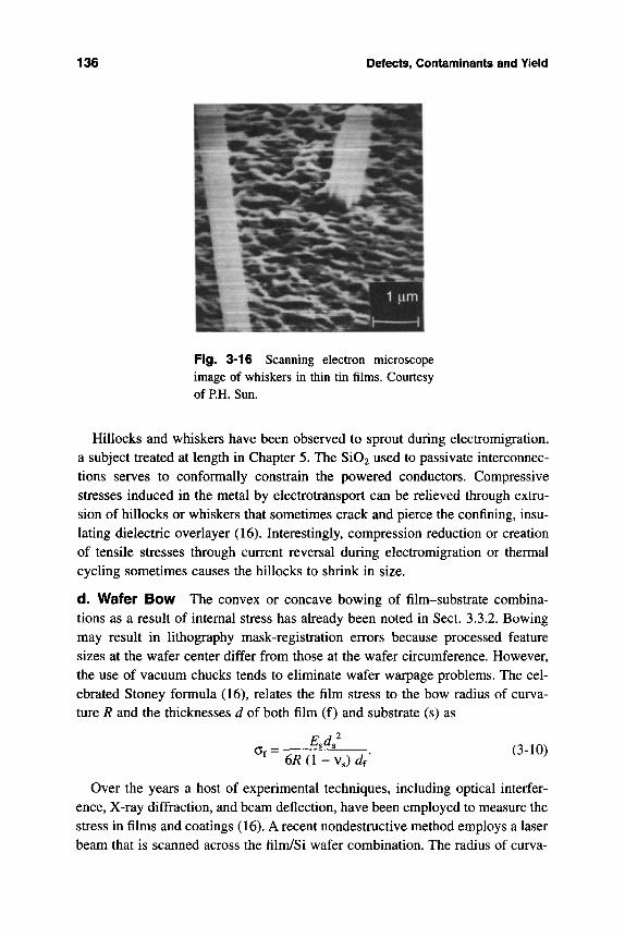
136 Defects, Contaminants and Yield
Fig. 3-16 Scanning electron microscope image of whiskers in thin tin films. Courtesy of P.H. Sun.
Hillocks and whiskers have been observed to sprout during electromigration, a subject treated at length in Chapter 5. The Si02 used to passivate interconnec-tions serves to conformally constrain the powered conductors. Compressive stresses induced in the metal by electrotransport can be relieved through extru-sion of hillocks or whiskers that sometimes crack and pierce the confining, insu-lating dielectric overlayer (16). Interestingly, compression reduction or creation of tensile stresses through current reversal during electromigration or thermal cycling sometimes causes the hillocks to shrink in size.
d. Wafer Bow The convex or concave bowing of film-substrate combina-tions as a result of internal stress has already been noted in Sect. 3.3.2. Bowing may result in lithography mask-registration errors because processed feature sizes at the wafer center differ from those at the wafer circumference. However, the use of vacuum chucks tends to eliminate wafer warpage problems. The cel-ebrated Stoney formula (16), relates the film stress to the bow radius of curva-ture R and the thicknesses d of both film (f) and substrate (s) as
Over the years a host of experimental techniques, including optical interfer-ence, X-ray diffraction, and beam deflection, have been employed to measure the stress in films and coatings (16). A recent nondestructive method employs a laser beam that is scanned across the film/Si wafer combination. The radius of curva-
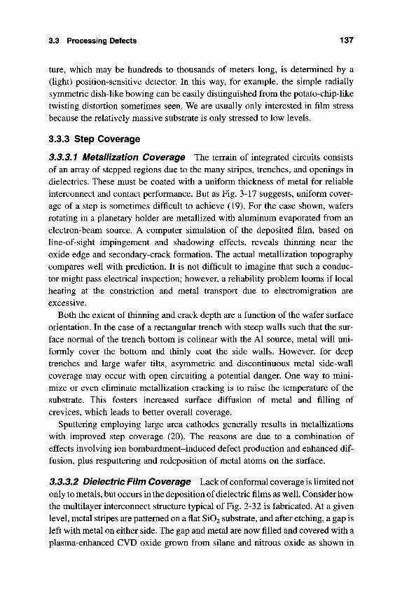
3.3 Processing Defects 137
ture, which may be hundreds to thousands of meters long, is determined by a (Hght) position-sensitive detector. In this way, for example, the simple radially symmetric dish-like bowing can be easily distinguished from the potato-chip-like twisting distortion sometimes seen. We are usually only interested in film stress because the relatively massive substrate is only stressed to low levels.
3.3.3 Step Coverage
3.3.3.1 Metallization Coverage The terrain of integrated circuits consists of an array of stepped regions due to the many stripes, trenches, and openings in dielectrics. These must be coated with a uniform thickness of metal for reliable interconnect and contact performance. But as Fig. 3-17 suggests, uniform cover-age of a step is sometimes difficult to achieve (19). For the case shown, wafers rotating in a planetary holder are metallized with aluminum evaporated from an electron-beam source. A computer simulation of the deposited film, based on line-of-sight impingement and shadowing effects, reveals thinning near the oxide edge and secondary-crack formation. The actual metallization topography compares well with prediction. It is not difficult to imagine that such a conduc-tor might pass electrical inspection; however, a reliability problem looms if local heating at the constriction and metal transport due to electromigration are excessive.
Both the extent of thinning and crack depth are a function of the wafer surface orientation. In the case of a rectangular trench with steep walls such that the sur-face normal of the trench bottom is colinear with the Al source, metal will uni-formly cover the bottom and thinly coat the side walls. However, for deep trenches and large wafer tilts, asymmetric and discontinuous metal side-wall coverage may occur with open circuiting a potential danger. One way to mini-mize or even eliminate metallization cracking is to raise the temperature of the substrate. This fosters increased surface diffusion of metal and filling of crevices, which leads to better overall coverage.
Sputtering employing large area cathodes generally results in metallizations with improved step coverage (20). The reasons are due to a combination of effects involving ion bombardment-induced defect production and enhanced dif-fusion, plus resputtering and redeposition of metal atoms on the surface.
3.3.3.2 Dielectric Film Coverage Lack of conformal coverage is limited not only to metals, but occurs in the deposition of dielectric films as well. Consider how the multilayer interconnect structure typical of Fig. 2-32 is fabricated. At a given level, metal stripes are patterned on a flat Si02 substrate, and after etching, a gap is left with metal on either side. The gap and metal are now filled and covered with a plasma-enhanced CVD oxide grown from silane and nitrous oxide as shown in
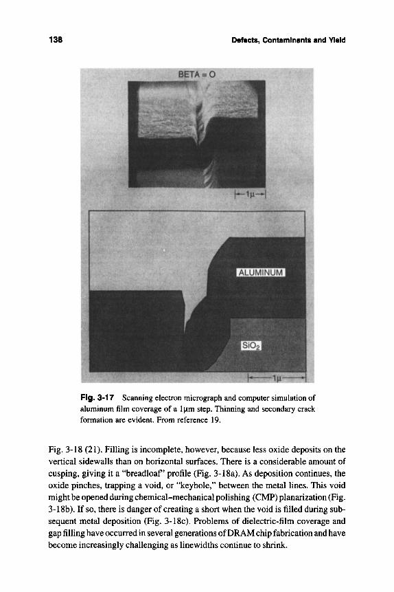
138 Defects, Contaminants and Yield
Fig. 3-17 Scanning electron micrograph and computer simulation of aluminum film coverage of a Ifxm step. Thinning and secondary crack formation are evident. From reference 19.
Fig. 3-18 (21). Filling is incomplete, however, because less oxide deposits on the vertical sidewalls than on horizontal surfaces. There is a considerable amount of cusping, giving it a "breadloaf' profile (Fig. 3-18a). As deposition continues, the oxide pinches, trapping a void, or "keyhole," between the metal lines. This void might be opened during chemical-mechanical polishing (CMP) planarization (Fig. 3-18b). If so, there is danger of creating a short when the void is filled during sub-sequent metal deposition (Fig. 3-18c). Problems of dielectric-film coverage and gap filling have occurred in several generations of DRAM chip fabrication and have become increasingly challenging as linewidths continue to shrink.
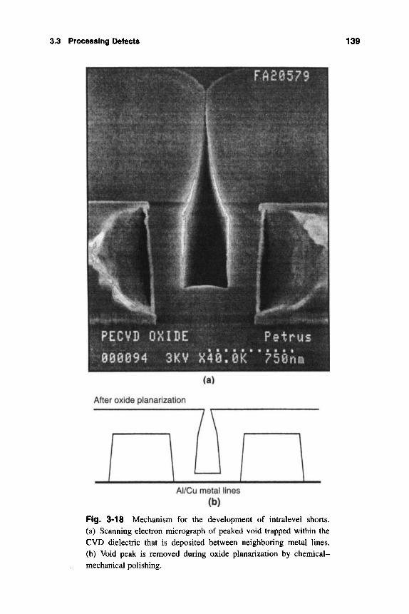
3.3 Processing Defects 139
After oxide planarization
Al/Cu metal lines (b)
Fig. 3-18 Mechanism for the development of intralevel shorts. (a) Scanning electron micrograph of peaked void trapped within the CVD dielectric that is deposited between neighboring metal lines. (b) Void peak is removed during oxide planarization by chemical-mechanical polishing.
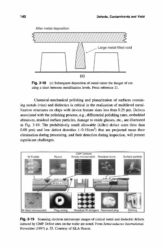
140 Defects, Contaminants and Yield
After metal deposition
Large metal-filled void
Fig. 3-18 (c) Subsequent deposition of metal raises the danger of cre-ating a short between metallization levels. From reference 21.
Chemical-mechanical polishing and planarization of surfaces contain-ing metals (vias) and dielectics is critical in the realization of multilevel metal-lization structures on chips with device feature sizes less than 0.25 jLim. Defects associated with the polishing process, e.g., differential polishing rates, embedded abrasives, residual surface particles, damage to oxide glasses, etc., are illustrated in Fig. 3-19. The prohibitively small allowable (killer) defect sizes (less than 0.08 |Lim) and low defect densities (~0.15/cm^) that are projected mean their elimination during processing, and their detection during inspection, will present significant challenges.
W Puddle Ripout CMP Defects
Empty microscratch Residual slurry Surface particle
|W-filled microscratch Plug coring Residual W stringers Recessed plug Dishing
Fig. 3-19 Scanning electron microscope images of critical metal and dielectric defects induced by CMP. Defect sites on the wafer are noted. From Semiconductor International, November (1997) p. 55. Courtesy of KLA-Tencor.
3.4 Contamination 141
3.4 CONTAiyilNATION
3.4.1 Introduction
High on the hst of defects in virtually every processing step entered in Ta-ble 3-4 is contamination. By this we usually mean foreign atoms, molecules, and particles that are chemically and physically different from the desired materials they inhabit. Contaminants can be gaseous, liquid, or solid in nature and can contaminate gaseous, liquid, and solid matrices. For example, gaseous matrices are contaminated by other gases, liquid droplets, and solid aerosol particles. Liq-uid matrices are contaminated by dissolved gas bubbles, droplets, and solid col-loid particles, and solid matrices by adsorbed gaseous and liquid surface films as well as particulates. Furthermore, contaminants can be ionic or nonionic, organic or inorganic.
Defects are manifested primarily in the form of particulate contaminants. For example, particulates have been estimated to be responsible for 75% or more of the loss in yield of volume manufactured VLSI chips (22). In view of this, it is not surprising that billions of dollars are spent annually by microelectronic chip manufacturers to combat contamination problems (23). A significant proportion of current articles and advertising in trade magazines like Solid State Technology and Semiconductor International is devoted to contamination and defect detec-tion or elimination issues. This reflects the magnitude and compelling nature of the problem. The sources of contamination in processing, the nature of particu-late contaminants, and the steps and strategies adopted to eliminate or minimize their influence are all addressed in this section.
Contamination of electronic products stems from essentially four sources: peo-ple, clean rooms, equipment, and processes. The impact of these on chip yield will be our primary focus of attention. Exposure to the environment also contaminates electrical products and sometimes leads to reliability problems. Environmental contamination used to adversely affect chip yields, but its impact has declined over the years through the widespread use of clean rooms. Nevertheless, package pro-cessing, which is not always done in clean rooms, is more susceptible to atmos-pheric contamination. Gone are the days when workers contaminated wafers with the cosmetics they wore, the dandruff they shed, or the salt they transported on their shoes during snowy mornings. Over the years the contaminant size has roughly reflected the finest features being processed. But the smaller the particle size, the more numerous and diverse their sources. Concurrently, circuit shrinkage has sig-nificantly reduced the size of contaminant particles that can be tolerated.
In the past, the distribution of contaminant sources was roughly evenly divided. Recent trends, however, show that people and clean rooms are less important con-tributors to contamination problems than equipment and processes. Nowadays,
142 Defects, Contaminants and Yield
contamination sources are quite subtle. Examples include airborne molecules, process gases (containing O2, N2, H2 O, etc., at -0.1-10 ppm levels), liquids (e.g., etching and cleaning solutions, even deionized water), as well as process cham-bers, tools, robots, and hardware (e.g., desorbed matter, wear particles). For exam-ple, in a variety of VLSI process tools involving vacuum hardware, baseline par-ticle levels are constant to a first approjcimation (24). However, this is punctuated by short bursts where particle counts may rise several fold above background as a result of opening or closing load-locks or transferring wafers. No tool, chemical, or rinsing solution is above suspicion. With this realization we now consider some examples of process-generated contaminants and their roles in fostering damage and yield loss. In contrast, environmental sources of contamination, e.g., corro-dents, and their effect on long-term reliability will be treated in Chapter 7.
3.4.2 Process-Induced Contamination
Many processes have proven to be culprits in generating contaminants ranging in size from the atomic to the particulate level. We shall also broaden our defin-ition to include charging of surfaces as a type of "contamination," in order to present the damage introduced during plasma etching.
It is instructive to view process contamination as a kind of "food chain," illus-trated in Fig. 3-20, that first involves generation and transport of particles, and then deposition on the wafer Implementing control measures to either eradicate their generation or transport, means that particles will not deposit.
Several processes known to generate contamination are briefly treated in turn.
3.4.2.1 Chemical Vapor Deposition It is believed that perhaps as much as 25% of all particle-induced yield loss is derived from low pressure CVD (LPCVD) processing (25). Among the films produced by LPCVD are silicon nitride, polysilicon, and (TEOS) Si02. Thin-film deposits naturally build up on the tubes of these hot-wall reactors during deposition. Film stress, along with the turbulence of loading wafers, causes shedding of these particulate deposits onto the wafer. Rubbing of quartzware in furnaces and oxidation and flaking of heaters are additional contamination sources.
Aside from impurities in the precursor gases, CVD processes can also gener-ate particulates from the gas-phase environment. The basic gas-to-solid film reaction is designed to occur at wafer substrates. However, when the supersatu-ration of reactants is too high, nucleation of the solid product may occur homo-geneously in the gas phase. In the form of "snow," the vapor-borne particulates settle on the substrate and are incorporated into the growing film. Generation of dislocations and stacking faults, regions of poor adhesion, and roughened film topographies are some of the adverse effects produced.
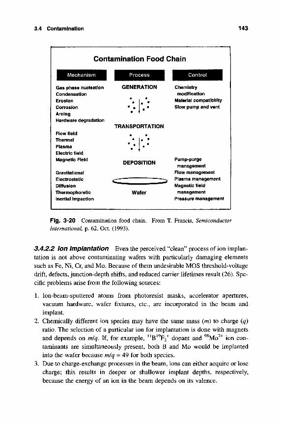
3.4 Contamination 143
Contamination Food Chain
Mechan ism
Gas piiase nucleation Condensation Erosion Corrosion Arcing hfardware degradation
Flow field Tiiermal Plasma Electric field Magnetic Field
Gravitational Electrostatic Diffusion Thermophoretic Inertial impaction
Process
GENERATION
• •
TRANSPORTATION
<=
•
• • •
• • • • •
DEPOSITION
Wafer
H Control
Chemistry modification
Material compatibility Slow pump and vent
Pump-purge management
Flow management ^ Plasma management
Magnetic field management
Pressure management
Fig. 3-20 Contamination food chain. International, p. 62, Oct. (1993).
From T. Francis, Semiconductor
3.4.2.2 Ion Implantation Even the perceived "clean" process of ion implan-tation is not above contaminating wafers with particularly damaging elements such as Fe, Mi, Gr, and Mo. Because of them undesirable MOS threshold-voltage drift, defects, junction-depth shifts, and reduced carrier lifetimes result (26). Spe-cific problems arise from the following sources:
1. lon-beam-sputtered atoms from photoresist masks, accelerator apertures, vacuum hardware, wafer fixtures, etc., are incorporated in the beam and implant.
2. Chemically different ion species may have the same mass (m) to charge (q) ratio. The selection of a particular ion for implantation is done with magnets and depends on m/q. If, for example, ^ B^ F2' dopant and ^ Mo " ion con-taminants are simultaneously present, both B and Mo would be implanted into the wafer because m/q = 49 for both species.
3. Due to charge-exchange processes in the beam, ions can either acquire or lose charge; this results in deeper or shallower implant depths, respectively, because the energy of an ion in the beam depends on its valence.
144 Defects, Contaminants and Yield
4. Cross contamination is common when implanters are called on to provide high fluences or fluxes for several different dopants. Thus, faster-diffusing boron and phosphorous dopants that contaminate arsenic and antimony implants displace junction depths. For example, a 0.01% contaminant level can cause a junction depth shift of 5%.
3.4.2.3 Plasma Processing During various film deposition and etching processes, devices are often directly exposed to an rf plasma discharge ambient of reactive ions, which are further accelerated by the wafer self-bias voltage. Enhanced and guided by the metallization or polysilicon patterns that act as "antennas," the result of these ion collisions is charging of the surface. Particu-larly large antenna surface areas may ultimately cause sufficient charge injection to degrade dielectric properties.
Damage to materials during plasma etching has been classified into two broad categories (27, 28):
1. Particle Current-Flow-Induced Damage. The buildup of charge produced by the plasma and the current driven by electric and magnetic fields are sources of this damage. Current flow through the dielectric produces wearout damage due to bond breaking and charge trapping.
2. Plasma Exposure Damage. This category of damage is a side effect of parti-cle or photon impingement on the surface. Residue layers, impurity perme-ation of the surface, and film adhesion damage due to photons or chemical attack are all examples of damage due to plasma exposure.
Particularly sensitive to plasma damage are gate oxides that have been shown to charge up, exhibit altered C-V curves (Sect. 2.5.2), and suffer earlier break-downs as a result. Fortunately, plasma damage effects often occur during overetching and not during the main etching (29). The subject of plasma damage to gate oxides is treated again in Sect. 6.3.8.
3.4.2.4 Lithography Just one glance at the defective mask in Fig. 3-21 reveals how patterned features on an IC chip can be severely damaged through incorporation of the indicated imperfections. Particulate contamination in the lithographic process is a chief contributor to such mask defects. Lithography defects of differing severity have been classified and include killers, unreliable, hard, soft, and repairable (30). Examples of these lethal defects are conductor opens and shorts through insulators between neighboring conductors. Unreliable defects do not cause immediate failures but may lead to long-term reliability problems. Pinholes and mouse bites that remove a small fraction of a patterned line are examples. Other unreliable defects include image density variations.
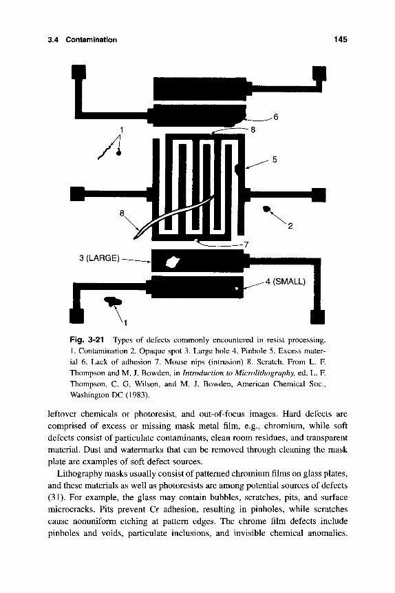
3.4 Contamination 145
Fig. 3-21 Types of defects commonly encountered in resist processing. 1. Contamination 2. Opaque spot 3. Large hole 4. Pinhole 5. Excess mater-ial 6. Lack of adhesion 7. Mouse nips (intrusion) 8. Scratch. From L. F. Thompson and M. J. Bowden, in Introduction to Microlithography, ed. L. F. Thompson, C. G. Wilson, and M. J. Bowden, American Chemical Soc, Washington DC (1983).
leftover chemicals or photoresist, and out-of-focus images. Hard defects are comprised of excess or missing mask metal film, e.g., chromium, while soft defects consist of particulate contaminants, clean room residues, and transparent material. Dust and watermarks that can be removed through cleaning the mask plate are examples of soft defect sources.
Lithography masks usually consist of patterned chromium films on glass plates, and these materials as well as photoresists are among potential sources of defects (31). For example, the glass may contain bubbles, scratches, pits, and surface microcracks. Pits prevent Cr adhesion, resulting in pinholes, while scratches cause nonuniform etching at pattern edges. The chrome film defects include pinholes and voids, particulate inclusions, and invisible chemical anomalies.
146 Defects, Contaminants and Yield
Chromium oxides, nitrides, and carbides are examples of the latter, and collec-tively they cause erratic local etching and undesired patterns.
Photoresists and the assorted chemical solutions used in lithography are also sources of contamination. They undergo extensive filtration to minimize the presence of particle and metal (e.g., Na, K) contamination.
3,4.2,5 MetBl Contamination Since the early days of Si device technology metallic contaminants have limited yield and been a reliability risk as well. In this regard, Kolbesen (12) has estimated that the iron present in a pinhead, if spread uniformly across the entire annual production of the world's leading wafer manu-facturer, would contaminate the wafers with a lethal dose of 10 ^ Fe atoms per cm . The gate oxide is particularly vulnerable to Fe, which lowers the dielectric breakdown voltage. In reducing the oxide thickness from 20 nm to 10 nm, corre-sponding to a translation from 1 |xm to 0.5 |xm linewidth technology, the Fe con-centration had to be lowered from 10* Fe atoms per cm^ to 10 ^ Fe atoms per cm , or a factor of 100 (32). The sources of metal contamination in production lines have been traced to virtually all tools, including furnaces and epitaxial reactors, ion implanters, plasma and reactive ion etching equipment, wet cleaning and etch-ing chemicals, and wafer handlers and equipment. A combination of harmful properties listed below causes metals to play a detrimental role in devices.
1. Transition metals such as Cu, Ni, Fe, and Cr are fast diffusers in Si. All have diffusivities exceeding 10" cm /s at temperatures of 1000°C. In particular, Cu, which is currently under consideration for use in metallizations, has a D value exceeding 10" cm /s even at 500°C, and an activation energy of less than 1 eV. This compares with D values of ~10~ ^ cm /s at 1000°C, and acti-vation energies of 3-4 eV for the common silicon dopants, i.e., B, P, and As.
2. Metals have a low solubility in Si (in the part per million and below range) with a steep temperature dependence. Trace impurities may dissolve in wafers at elevated processing temperatures but be supersaturated when cooled to room temperature. Their rejection from solution leads to precipita-tion of silicides, e.g., FeSi2 and NiSi2, at lattice defect nucleation sites.
3. Many transition metals are effective minority carrier recombination and gen-eration centers because they form levels within the Si band gap. In addition, these metals react with acceptor impurities,
4. Metal precipitates serve as nuclei for the generation of extended defects such as dislocations and oxygen-induced stacking faults in the Si substrate and gate oxide.
5. Metal decoration of existing defects makes them far more conducting. Dislo-cations and stacking faults so affected have caused excessive leakage currents in p-n junctions and retention time failures in DRAMs.
3.4 Contamination 147
A chronic metal contaminant of interest in microelectronics is sodium. In ionic form it inhabits the various oxides and glasses of the IC chip. Sodium is now largely eliminated from gate oxides, where it causes threshold voltage insta-bilities in MOSFET operation at surface densities above 1 x 10^%m^. Presently, Na concentrations ranging from 10 '' to 10^ atoms/cm^ are found above the met-alUzation levels, and are primarily introduced via photoresists (33).
3.4.3 Introduction to Particle Science
To develop strategies for reducing particulate contamination levels in microelec-tronics, it is important to understand the nature of particles, the way they are transported, and their mechanisms of adhesion to surfaces and wafers in partic-ular (34). The most important attribute of a particle is its size, because properties such as particle velocity, adhesion force, and ability to scatter light depend on it. There are vast differences in the behavior of large-scale objects compared to the submicron-sized particles that are our present concern. For example, the latter will adhere quite strongly to the ceiling of a chamber, but a 1 mm particle will immediately drop because gravitational forces far exceed the very weak adhe-sion forces. In microelectronic processing, drag, gravitational, and diffusional forces spread contamination by driving particles to wafer surfaces where various forces of adhesion (e.g., van der Waals, electrostatic, capillary) cause them to stick. Overcoming the influence of particle adhesion forces is a way to combat contamination. For these reasons, each of the forces will be briefly discussed in turn.
3.4.3. f Drag As particles move through a fluid (gas or liquid) they are opposed by frictional drag forces. For a small spherical particle of diameter d, moving slowly with velocity v, the drag force is given by Stokes's law, or
Frf = 37tr| ^ v/Ce. (3-11)
Here r| is the coefficient of viscosity, and Q is the Cunningham slip correction factor. For air at 1 atm and 20°C, Q = 1 4- 0.16/d, with j? given in |im units. Thus, for particles smaller than 0.5 |im in size, Q becomes significant. Equation 3-11 is well satisfied when the Reynolds number for gas flow, defined by d vpf/r| (Pf = fluid density), is less than 1; this is generally a good assumption for micro-electronic processing.
3.4.3.2 Gravity Of all the forces that act on aerosol particles, gravity is espe-cially important because it acts all the time. The gravitational force is given by
F, = -iPp-pdg, (3-12)
148 Defects, Contaminants and Yield
where pp is the particle density and g is the gravitational constant. By equating Fd and Fg, the terminal velocity with which particles fall by gravity is given by
d^ (PD - Pf) Ccg v = \^ . (3-13)
18 Ti
Gravity always enhances the rate of particle impingement on the surface of a wafer. The deposition flux, which is the product of the particle concentration and velocity, will be small if v is small. Importantly, particle impingement rates fall off as the square of the particle size.
3.4.3.3 Diffusion The constant buffeting and bombardment by fluid mole-cules causes small particles to execute Brownian diffusive motion. Such random motion becomes important when the particle is less than 1 |im in size. Diffusion distances are given by the familiar formula, x^ = ADt, (see Eq. 5-6), where D is the diffusion coefficient and t is the time. Theory shows that D is given by D = Q kTK^TV^d), where kT has the usual meaning. Clearly, smaller particles are expected to travel further. We are often concerned with the rate of particle impingement on wafers as a result of diffusion through the surrounding gas phase. Because small particles readily adhere to surfaces, their concentration (Q is lower there than in the bulk gas. This gradient (dC/dx) establishes a diffusive flux (J) of particles toward the surface given by D dCldx. Assuming that the wafer is immersed in an ambient where the particle concentration is Q , the rate of particle impingement (number per unit area per unit time) due to diffusion is given by
J - C . ^ , (3-14)
a result that can be obtained from Eq. 5-4 by differentiating. The number of par-ticles N(t) that accumulate in time is simply the integral of this, or
where Q is the particle concentration far from the surface. A comparison of the particle densities that settle on a surface by diffusion relative to gravity is shown in Fig. 3-22. Whereas gravitational settling dominates for large particle diame-ters, diffusional impingement controls when the particle size is small. It is important to note that Brownian motion distances are the same order of magni-tude as the thin boundary layer thickness of gas flowing by surfaces. Thus diffu-sion enables particles to penetrate this stagnant layer, reach the surface, and col-lect there. The expected particle flux is also indicated in Fig. 3-22. Due to the low concentration of large particles, there is a decline in impingement flux at these particle sizes.
3.4 Contamination 149
10
0.001 t-
"T 1 I I I I M I - I 1—\ I I I M I 1 1—r
/ / 'A
0.1 1 Particle Diameter, |im
Fig. 3-22 Number of particles collected per square centimeter of hori-zontal surface by diffusion (solid line) and gravity (dashed line), as a func-tion of particle size. Particle density = Ig/cm , Particle concentration = 1/cm , Temperature = 20°C. From reference 34.
3.4.3.4 Electrostatic Forces Initially uncharged particles often acquire charge through interaction with ionic species and gas molecules that become charged by ionizing radiation. The probability (Pg) that n electronic charges (both positive and negative) are associated with particles is governed by their size (d) according to a Maxwell-Boltzmann-type expression
P = const (d klf' exp
2 2
dkT (3-16)
Thus, very small particles will be uncharged. For particles larger than 0.1 |im, the average n increases with d as n = 2.37 (t/ m) ^ (35). Charged particles will interact with one another according to Coulomb's law.
3.4.3.5 Particle Adhesion Particles adhere to surfaces through van der Waals, electrostatic, and capillary forces as well as chemical (hydrophobic/ hydrophilic) interactions. Soluble contaminants are effectively removed by
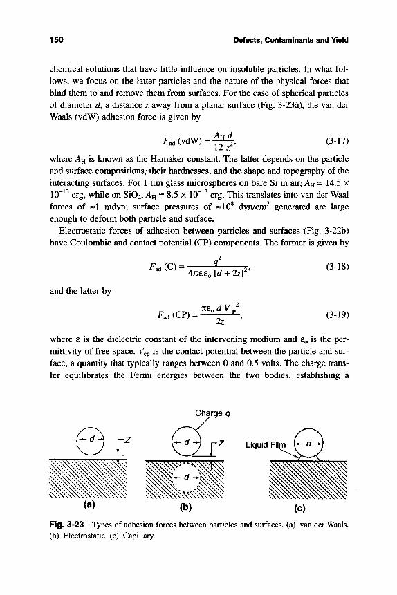
150 Defeats, Cohtaminanls and Yield
chemical solutions that have little influence on insoluble particles. In what fol-lows, we focus on the latter particles and the nature of the physical forces that bind them to and remove them from surfaces. Fdir the case of spherical particles of diameter d, a distance z away from a planar surface (Fig. 3-23^), the van der Waals (vdW) adhesion force is given by
Fac,(vdW) = ^ , (3-17)
where AH is known as the Hamaker constant. The latter depends on the particle and surface compositions, their hardnesses, and the shape and topography of the interacting surfaces. For 1 m glass microspheres on bare Si in air; AH =14.5 x 10"^^ erg, while on Si02, AH = 8.5 x 10" ^ erg. This translates into van der Waal forces of «1 mdyn; surface pressures of «10^ dyn/cm^ generated are large enough to defbtm both particle and surface.
Electrostatic forces of adhesion between particles and surfaces (Fig. 3-22b) have Coulombic and contact potential (CP) components. The former is given by
F^iC) = 47ceeo [d^lzf
and the latter by
TOO d VcD^
2z
(348)
(3-19)
where e is the dielectric constant of the intervening medium and EQ is the per-mittivity of free space. Vcp is the contact potential between the particle and sur-face, a quantity that typically ranges between 0 and 0.5 volts. The charge trans-fer equilibrates the Fermi energies between the two bodies, estabhshing a
Charge q
Liquid
Fig. 3-23 Types of adhesion forces between particles and surfaces, (a) van der Waals. (b) Electrostatic, (c) Capillary.
3.4 Contamination 151
capacitor-like double layer at the interface. Generally for small particles, adhe-sion forces due contact potential exceed those due to electrostatic attraction. For a 1 ^m particle, with z = 4 x 10"^ cm and Vcp = 0.5 V, F d (cp) « 1 tndyn. This force is roughly comparable to that for van der Waals interactions.
In humid environments adhesion between particles and the surface is pro-moted by the intervening water film that develops between them because of cap-illary attraction (Fig. 3-23c). A capillary force (Fc) of amount
F^ = 2ndy (3-20)
can be expected, where y is the surface tension of water (72 dyn/cm). For a 1 |im particle, Fc = 4.5 x 10"^ dyn, a force that is larger than others considered above.
3.4.3.6 GleBtfing Particle removal from wafer surfaces means establishing external forces that exceed the forces of adhesion. These external forces can be divided into three categories (35): vibratory or mechanical action, hydrodynamic or aerodynamic drag, and wet or dry chemical action. Specific wafer-cleaning techniques include scrubbing, high-pressure gas or liquid jets, wet chemical methods, and ultrasonic, ultraviolet or ozone cleans.
Scrubbing. In this mechanical technique a brush rotates across the surface, removing inorganic particles and organic films. Like a car hydroplaning on a wet highway, the hydrophilic (water attracting) brush bristles are separated from the wafer surface by the thin layer of scrubbing solution. Scrubbing effectively removes large particles (> Ijiim) from hydrophobic (water repelling) wafer sur-faces. But scrubbing is unsuitable for submicron particle removal, especially from patterned wafers, and may even cause damage.
Pressurized fluid jets. This method of cleaning will remove small particles from patterned wafers. As the fluid moves past particles with velocity v, it drags them with a force given by Eq. 3-11. Higher velocities and viscosity coefficients are more effective in cleaning. As a consequence, the drag force is considerably higher with fluid than with gas jets. Troublesome static charge buildup on wafers and the possibility of mechanical damage are disadvantages.
Ultrasonics. High-intensity sound waves at frequencies above 20 kHz are employed in this technique. They produce mechanical pressure fluctuations that result in the formation of cavitation bubbles. During the pressure cycle, the bub-bles alternately expand and collapse. At the collapsing bubble interface, suffi-cient energy is released locally at particles to overcome the force of adhesion and loosen them. While small particles are efficiently removed, it is difficult to control cavitation without causing possible wafer damage.
152 Defects, Contaminants and Yield
Wet chemical cleaning. This widely used wafer decontamination method effectively removes metal ions and soluble impurities, but is not good for parti-cle removal. Because assorted acids and bases are used, rinsing and drying steps are required. In addition, particulate contamination is often present in chemical solutions.
Ultraviolet or ozone. Dry processing and contactless removal of organic contamination are advantages of this cleaning technique. However, this method is not proven for particle removal.
3.4.4 Combating Contamination
3.4.4.1 Particle Detection The first step in developing a plan for contami-nation control is to be able to confidently detect and analyze particle size and chemistry of samples. For this purpose instruments have been developed to mea-sure particles in gases and liquids as well as on solid surfaces (wafers). Instru-ment capabilities include sensitivity (e.g., how small a particle can be detected), selectivity (e.g., ability to not mistakenly respond to something other than what is sought), rate of sampling and dynamic range, or the ratio of the highest to low-est level (e.g., particle size, concentration). Needless to say, high sensitivity, selectivity, rate of sampling, and dynamic range are essential.
In general, optical scattering techniques are employed for particle size and distribution measurements. Larger particles and those of higher refractive index than the surrounding media tend to scatter more light than smaller and lower refractive index particles. (However, this is not always true.) Rayleigh (dipole) scattering dominates when the particles are much smaller than the wavelength of light used, and yields a signal proportional to the square of the particle volume. Geometrical optics prevail when the particles are much larger than the wave-length, and scattering then occurs by reflection and refraction. Between these size-range extremes there is Mie scattering. Particle sizes of less than 100 nm can be detected by available instruments, which typically employ computerized image analysis or holography techniques. This equipment and questions of what to sample for, where to sample, how many samples to take, how to interpret a count of zero, and how to analyze data are discussed by Cooper (23).
3.4.4.2 Clean Rooms The use of clean rooms has traditionally been the chief strategy in combating contamination and particle-induced defects. Moni-toring particulate contamination and controlling processing variables, through feedback and feedforward of defect information, help establish high yields for process steps carried out in the clean room. Air whose temperature and humid-ity are tightly controlled enters clean rooms through efficient particulate air fil-
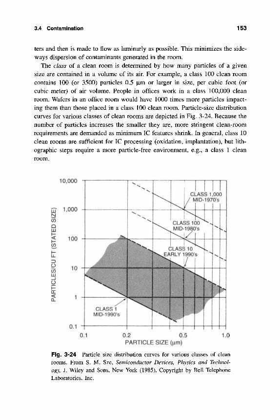
3.4 Contamination 153
ters and then is made to flow as laminarly as possible. This minimizes the side-ways dispersion of contaminants generated in the room.
The class of a clean room is determined by how many particles of a given size are contained in a volume of its air. For example, a class 100 clean room contains 100 (or 3500) particles 0.5 |Lim or larger in size, per cubic foot (or cubic meter) of air volume. People in offices work in a class 100,000 clean room. Wafers in an office room would have 1000 times more particles impact-ing them than those placed in a class 100 clean room. Particle-size distribution curves for various classes of clean rooms are depicted in Fig. 3-24. Because the number of particles increases the smaller they are, more stringent clean-room requirements are demanded as minimum IC features shrink. In general, class 10 clean rooms are sufficient for IC processing (oxidation, implantation), but lith-ographic steps require a more particle-free environment, e.g., a class 1 clean room.
10,000
UA 1,000 N CO Q UJ
!^ H
t O CO LU _ l
o H DC < a.
100
0.2 0.5 PARTICLE SIZE ( im)
1.0
Fig. 3-24 Particle size distribution curves for various classes of clean rooms. From S. M. Sze, Semiconductor Devices, Physics and Technol-ogy, J. Wiley and Sons, New York (1985), Copyright by Bell Telephone Laboratories, Inc.
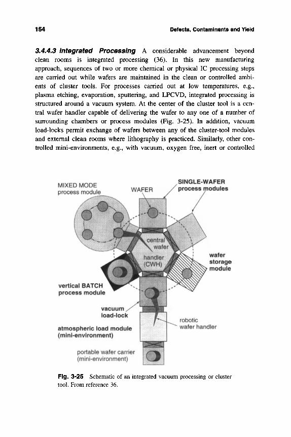
154 Defects, Contaminants and Yield
3,4.4.3 Integrated Processing A considerable advancement beyond clean rooms is integrated processing (36). In this new manufacturing approach, sequences of two or more chemical or physical IC processing steps are carried out while wafers are maintained in the clean or controlled ambi-ents of cluster tools. For processes carried out at low temperatures, e.g., plasma etching, evaporation, sputtering, and LPCVD, integrated processing is structured around a vacuum system. At the center of the cluster tool is a cen-tral wafer handler capable of delivering the wafer to any one of a number of surrounding chambers or process modules (Fig. 3-25). In addition, vacuum load-locks permit exchange of wafers between any of the cluster-tool modules and external clean rooms where lithography is practiced. Similarly, other con-trolled mini-environments, e.g., with vacuum, oxygen free, inert or controlled
MIXED MODE process module
SINGLE-WAFER process modules
vertical BATCH process module
atmospheric load module (mini-environment)
portable wafer carrier (mini-environment)
wafer storage module
robotic wafer handler
Fig. 3-25 Schematic of an integrated vacuum processing or cluster tool. From reference 36.
3.5 Yield 155
gas ambients enable cleaning, CVD deposition of dielectric films, reactive ion etching, rapid thermal annealing, and oxidation to be carried out. The greatly enhanced cleanliness results in lower contamination levels of particulates and reactive impurities. In effect, processing in cluster tools occurs in a class 0.1 clean room.
3.5 YIELD
3.5.1 Definitions and Scope
Yield is generally defined as the ratio of the number of good products produced to the total number of units started in any manufacturing operation (37). The denominator of this ratio is the sum of the good products and those that had the potential of being good but for some reason were rejected. It should be clear that yield affects the cost of semiconductor products and our ability to predict their price in advance. Yield and cost are the crucial issues that determine the eco-nomic success or failure of semiconductor processing and manufacturing indus-tries. The expected inverse correlation between yield and processing defects is depicted in Fig. 3-26. Despite wide swings in the monthly tracking of product yield, the trend is inexorably upward as learning occurs. It has been suggested that there are links between defects and reliability as well. Thus logic would dic-tate that yield and reliability are related despite the fact that the latter presum-ably refers solely to the performance of good, or yielded, products.
Product yields are generally less than 100% for the following reasons;
1. Circuit design problems. This may simply be due to errors in circuit design. The celebrated discovery in 1994 of omitted circuits within the 3 million transistor Pentium microprocessor chip is an example. Although the manufactur-ing yield of this chip was certainly satisfactory initially, the subsequent recall and substitution had the same economic impact as drastically reduced yield. Other problems arise from alteration of circuit parameters beyond acceptable limits due to processing difficulties, which are then not accommodated in the design. New device behavior or circuit characteristics, unforeseen by the designer, sometimes surface to the detriment of yield. Some circuits are rela-tively tolerant to variations in circuit parameters, while others are very sensitive. In such cases an interactive effort between the designer (who identifies sensitive parameters) and process engineer (who optimizes the value and range of these
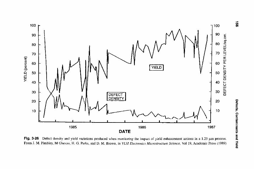
100
90
80
70 h c
a
a n 2 60
v
9 50 w
40
30
20
10
I- - 100
- 90 g c! 0-
80 5 W >
70 5 CT W
60 a
50 $
40 i-
30
20
10
-
-
-
c
Y
- W n -
-
-
-
t I I I I I I -
1985 1986 1987 DATE
Fig. 3-26 Defect density and yield variations produced when monitoring the impact of yield enhancement actions in a 1.25 pm process. From J. M. Pimbley, M Ghezzo, H. G. Parks, and D. M. Brown, in VLSZ Electronics Microstructure Science, Vol 19, Academic Press (1989)
P) a n
3.5 Yield 157
parameters) is required for redesign and tuning of one or more process steps. Circuit design problems are well beyond the scope of this book and will not be discussed further.
2. Processing defects. Processing is frequently accompanied by inadver-tent changes in the dimensions and composition of device features and compo-nents that adversely affect yield. Examples of such processing defects and their impUcations were discussed at length throughout this chapter.
3. Random point defects. Even though processing parameters are well within design specifications, the yield may still be below 100%. The reason is usually attributed to point defects or particles of macroscopic dimensions that settle on the wafer or obstruct the proper execution of a given processing step. Dust particles on a lithography mask is an example of the latter. These and other random defects can be killers. Often, however, a less-than-killer defect survives screening and becomes the nucleus for eventual failure in service.
For any series of IC manufacturing steps, the overall, or cumulative, yield (Y) is the product of the wafer process yield (Y^), the wafer test yield (Yi), and the module test yield (Fm), such that
F = ( y j x ( F t ) x ( F J . (3-21)
Rejects occur at each stage where yield is evaluated, i.e., during individual pro-cessing steps including epitaxy, oxidation, metallization, metal removal, electrical testing of scribed and diced fabricated chips, and final testing of packaged and assembled modules. Therefore, F^, Ft, and F^ are each similarly defined by the above generic yield definition. Because of the many hurdles that must be sur-mounted during these rigorous evaluation procedures it is remarkable that the quality and reliability of semiconductor electronics is excellent. However, there is always room for improvement, and this section is dedicated to that end.
3.5.2 Statistical Basis for Yield
A functional definition of yield is the probability of producing chips having no fatal defects that would cause immediate rejection. Yield prediction, therefore, requires calculating the probability of finding a particular state (a chip with no defects) out of all possible states (chips with 0, 1, 2 or more defects) when the events or defects are statistically distributed over all states according to some distribution function (38).
It is instructive to start by introducing the statistics of the binomial distribu-tion, which can be physically described by the tossing of coins that have two outcomes—heads or tails. This subject is discussed in virtual every text on
158 Defects, Contaminants and Yield
statistics and probability. If the probability of getting a head in one trial toss isp and the probability of getting a tail is q, then it is evident that p + q = 1. (In an unbiased coin p = q = \)' The same holds for A tosses, where the probability of obtaining at least one head or at least one tail is unity, or (p + q)^ = 1. Expan-sion yields
an equation known as the binomial distribution. Extending the result to A coins each flipped once or one coin flipped A times, the probability (P) that n heads will be obtained in A tosses is
A ' Pin; N, p) = ;'' p"" (1 - pf-\ (3-23)
In a simple example, consider 3 coins that are tossed once. What is the proba-bility of getting exactly 2 heads? There are 8 possible outcomes (hhh), (hht), (hth), (htt), (ttt), (tth), (tht), and (thh), and of these 3 have two heads. Thus the probability we seek is | . This answer also results from direct substitution of N = 3,n = 2,p = im which case P = 3!/(2! 1!) x ({f ({Y = | .
With no loss in generality let us consider Eq. 3-23 under conditions where N is large, i.e., N» I, N» n, and p is small; but the product Np = a is of mod-erate size. Next, the following quotient of factorials and polynomials is expanded,
^- =N(N-l)(N-2) . . .(N-[n-l]) = (N-n)\
N". N
(l-pf-n = c^p{(N-n)ln(l-p)}=cxp{-iN-n)(p-^ip^ + ip' + . . .)}
= exp {-Np (I +YP -\-JP^ -\-. . ,)} = exp [-Np] or exp [-a].
Upon substitution in Eq. 3-23,
P(n; N,p) = exp [-a]. (3-24)
This result is the Poisson approximation to the binomial distribution. What does all of this have to do with yield? Suppose now that a number of
events (defects) occur randomly in adjacent, nonoverlapping domains, and that
3.5 Yield 159
these events are independent of events in other areas. The probability of a chip containing n defects is then given by Eq. 3-24. Thus the probability of a chip containing zero defects, a quantity previously defined as the yield, is given by
p (0, Np) = P (0, a) = 7 = exp [-a]. (3-25)
Furthermore, suppose the domain is the chip of area A, and a is the average number of events or fatal defects per chip. If the defect density or number of defects per unit area is D, then a = DA, and
y=exp[-DA]. (3-26)
This important equation expresses the probability of a chip having no defects provided that the defect density is constant. The strong exponential decrease in yield with increase in A and D should be appreciated. As a consequence of enlarging the die area from 1 cm^ to 1.5 cm^ the yield will drop by a factor equal to exp [- (1.5 - 1.0)D], assuming the same D; for example, the respective fac-tors are 0.78 and 0.61 when D = 0.5 and 1 defect/cm^. Imperatives to lower D when increasing the wafer size are thus evident. The fundamental relationship expressed in Eq. 3-26 is the basis for yield modeling, a subject treated next.
3.5.3 Yield Modeling
Instead of being constant, assume now that the defect density varies according to the function/(Z>). Then the probability that a chip will have n defects is given by the Poisson equation, i.e.,
'{n,DA)=l •'n ni
When n = 0 the yield is calculated as
Y= I j{D) exp [-DA] dD. (3-28)
This integral, proposed by Murphy (39), plays an important role in yield model-ing. Depending on the form of the function fiP), different yields are obtained when evaluating the integral. Among the many defect-density functions sug-gested over the years, the following have been found useful:
1. Constant D. In the case where D is a constant (i.e.. Do), we require that/(D) = 0 everywhere except for D = Do- Mathematically,/(D) = 5 (D - Do), and / behaves like a delta function (5). Substitution into Eq. 3-28 and integration yields our expected formula
160 Defects, Contaminants and Yield
7=exp[ -DoA] . (3-29)
2. Triangular. This approximation to a Gaussian distribution has the form/(D) = DID^^ for Do > D > 0, and/(D) = \ID^ (2 - DID^) for 2D^>D> D^. When D > 2Do,/(D) = 0. Substitution into Eq. 3-28 and integration yields
_ ( l - e x p [ - D o A ] )
3. Exponential. In this case J{D) = 1/Do exp [- D/DQ], and substitution into Eq. 3-28 yields
y=( l+DoA)-^ (3-31)
after integration.
Graphic representations of these as well as Gaussian and gamma distribution functions of D are shown in Fig. 3-27. The shape of these functions depends on the value of a, the standard deviation normalized with respect to DQ. In the case of the ganmia function, when a = 1 we have the simple exponential function. Plots of normalized yield behaviors for the three-parameter gamma distribution as a function of the defect density-area product are displayed in Fig. 3-28. For values of a different from zero, yields are always greater than that given by Eq. 3-29.
The reader should not be lulled into thinking that just because mathematical equations for yield exist, f(D) can actually be predicted. In fact, quite the oppo-site is true. Presently, there is no way to determine J{D) directly. Instead, it is inferred from actual production yields by curve fitting. Once obtained, /(D) can be said not to be wrong if calculated yields derived from it match the production experience. Nevertheless, there is no reason to assume that /(D) derived for product A will apply to product B, or even product A in another time frame and environment.
3.5.4 Comparison with Experience
Yields generally improve over time as learning occurs. For new products the ini-tial yield may be close to zero. But, by establishing yield targets, monitoring actual performance, prioritizing yield detractors, implementing action, and then iterating improvement cycles of successively shorter duration, yields rise slowly at first, then more rapidly, until product yields level off at ~ 90% or more. Simul-taneously, defect densities are observed to fall in concert.
Among other findings concerning yield are the following:
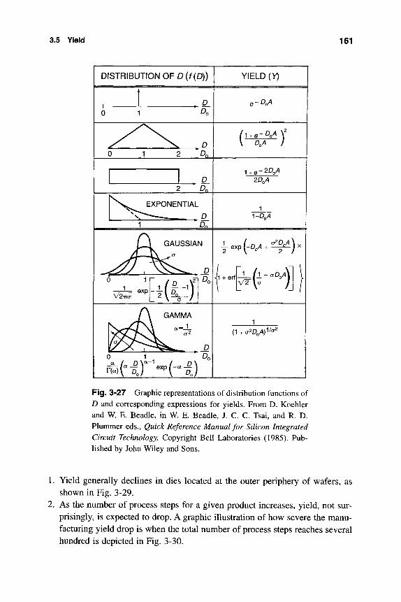
3.5 Yield 161
DISTRIBUTION OF D {f(D)) YIELD (V)
-D^A
V D,A J
2D^A Dn
GAUSSIAN
1 + erf
GAMMA
(1 +(T^D^A)^^^^
M'iTM-i) Fig, 3-27 Graphic representations of distribution functions of D and corresponding expressions for yields. From D. Koehler and W. E. Beadle, in W. E. Beadle, J. C. C. Tsai, and R. D. Plummer eds.. Quick Reference Manual for Silicon Integrated Circuit Technology, Copyright Bell Laboratories (1985). Pub-lished by John Wiley and Sons.
1. Yield generally declines in dies located at the outer periphery of wafers, as shown in Fig, 3-29.
2. As the number of process steps for a given product increases, yield, not sur-prisingly, is expected to drop. A graphic illustration of how severe the manu-facturing yield drop is when the total number of process steps reaches several hundred is depicted in Fig. 3-30.
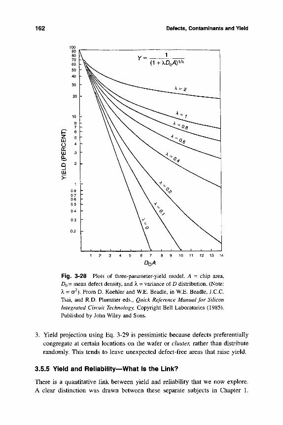
162 Defects, Contaminants and Yield
11 12 13 14
DQA
Fig. 3-28 Plots of three-parameter-yield model. A = chip area, Do = mean defect density, and X = variance of D distribution. (Note: X = a^). From D. Koehler and W.E. Beadle, in W.E. Beadle, J.C.C. Tsai, and R.D. Plummer eds.. Quick Reference Manual for Silicon Integrated Circuit Technology, Copyright Bell Laboratories (1985). Published by John Wiley and Sons.
3. Yield projection using Eq. 3-29 is pessimistic because defects preferentially congregate at certain locations on the wafer or cluster, rather than distribute randomly. This tends to leave unexpected defect-free areas that raise yield.
3.5.5 Yield and Reliability—What Is the Link?
There is a quantitative link between yield and reliability that we now explore. A clear distinction was drawn between these separate subjects in Chapter 1.
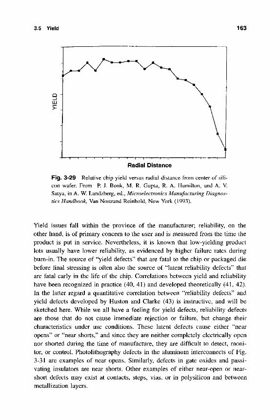
3.5 Yield 163
Radial Distance
Fig. 3-29 Relative chip yield versus radial distance from center of sili-con wafer. From P. J. Bonk, M. R. Gupta, R. A. Hamilton, and A. V. Satya, in A. W. Landzberg, ed.. Microelectronics Manufacturing Diagnos-tics Handbook, Van Nostrand Reinhold, New York (1993).
Yield issues fall within the province of the manufacturer; reliability, on the other hand, is of primary concern to the user and is measured from the time the product is put in service. Nevertheless, it is known that low-yielding product lots usually have lower reliability, as evidenced by higher failure rates during bum-in. The source of "yield defects" that are fatal to the chip or packaged die before final stressing is often also the source of "latent reliability defects" that are fatal early in the life of the chip. Correlations between yield and reliability have been recognized in practice (40, 41) and developed theoretically (41, 42). In the latter regard a quantitative correlation between "reliability defects" and yield defects developed by Huston and Clarke (43) is instructive, and will be sketched here. While we all have a feeling for yield defects, reliability defects are those that do not cause immediate rejection or failure, but change their characteristics under use conditions. These latent defects cause either "near opens" or "near shorts," and since they are neither completely electrically open nor shorted during the time of manufacture, they are difficult to detect, moni-tor, or control. Photolithography defects in the aluminum interconnects of Fig. 3-31 are examples of near opens. Similarly, defects in gate oxides and passi-vating insulators are near shorts. Other examples of either near-open or near-short defects may exist at contacts, steps, vias, or in polysilicon and between metallization layers.
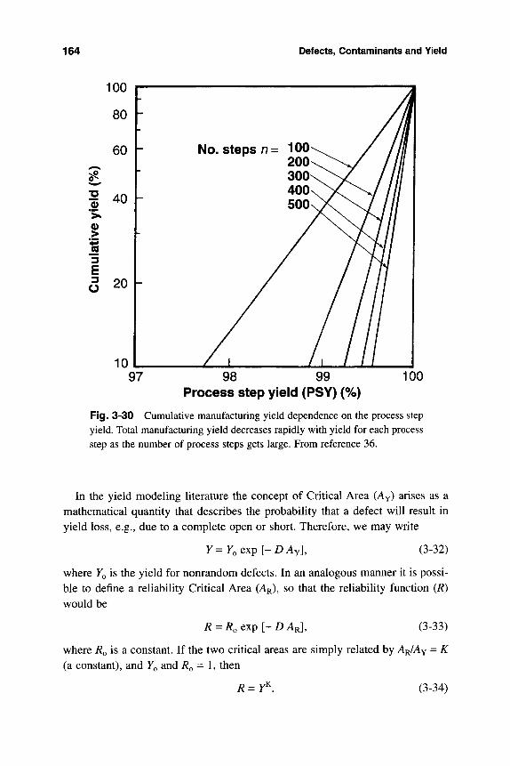
164 Defects, Contaminants and Yield
100
80
60 h
> 0) > HM
(0 3 E 3
o
40
20
10
r [- No. 1-
r~
U
steps n =
-J
100^ / / / I 2 0 0 ^ ^ / / / / / 3 0 0 \ \ / / / / / 4 0 0 \ N < \ / / / / 5 0 0 N X \ 7 / / /
U / / / 97 98 99
Process step yield (PSY) (%) 100
Fig. 3-30 Cumulative manufacturing yield dependence on the process step yield. Total manufacturing yield decreases rapidly with yield for each process step as the number of process steps gets large. From reference 36.
In the yield modeling literature the concept of Critical Area (Ay) arises as a mathematical quantity that describes the probability that a defect will result in yield loss, e.g., due to a complete open or short. Therefore, we may write
Y=Y,CXP[-DAYI (3-32)
where Y^ is the yield for nonrandom defects. In an analogous manner it is possi-ble to define a reliability Critical Area (AR), SO that the reliability function (R) would be
R = R,cxp[-DAj,l (3-33)
where R^ is a constant. If the two critical areas are simply related by A^/Ay = K (a constant), and Y^ and RQ=\, then
/? = y^ (3-34)
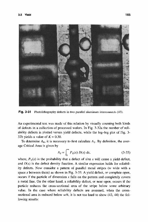
3.5 Yield 165
Fig. 3-31 Photolithography defects in two parallel aluminum interconnects (43).
An experimental test was made of this relation by visually counting both kinds of defects in a collection of processed wafers. In Fig. 3-32a the number of reli-ability defects is plotted versus yield defects, while the log-log plot of Fig. 3-32b yields a value ofK= 0.30.
To determine AR, it is necessary to first calculate Ay. By definition, the aver-age Critical Area is given by
' = [ PY(X) D(X) dx, ^
(3-35)
where, PY(X) is the probability that a defect of size x will cause a yield defect, and D(x) is the defect density function. A similar expression holds for reliabil-ity defects. Now consider a pattern of parallel metal stripes (w wide with a space s between them) as shown in Fig. 3-33. A yield defect, or complete open, occurs if the particle of dimension x falls on the pattern and completely covers a metal line. On the other hand, a reliability defect, or near open, occurs if the particle reduces the cross-sectional area of the stripe below some arbitrary value. In the case where reliability defects are assumed, when the cross-sectional area is reduced below w/4, it is not too hard to show (43, 44) the fol-lowing results:
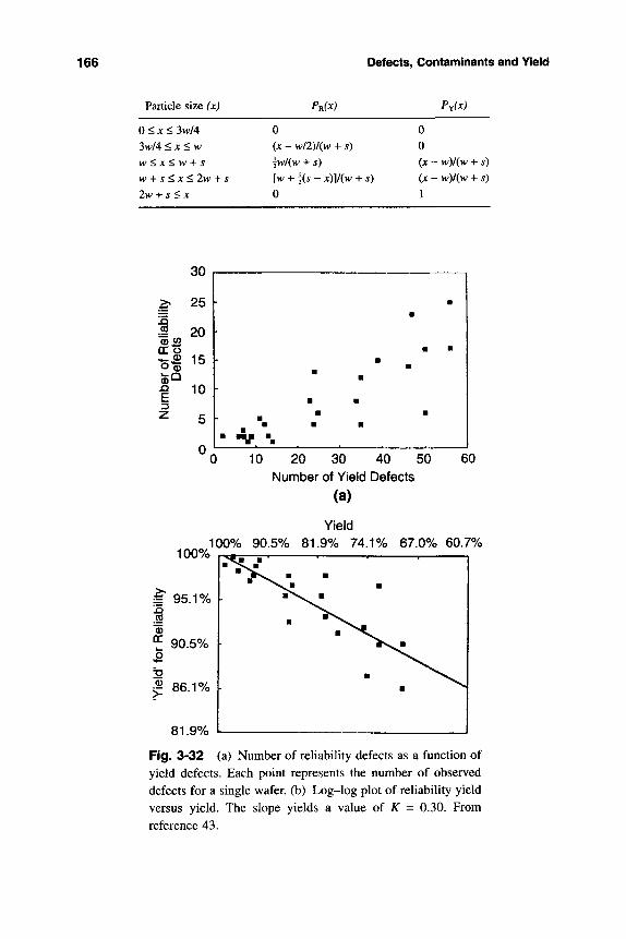
166 Defects, Contaminants and Yield
Particle size (x)
0 < jc < 3w/4 3w/4 < JC < w w <x<w + s w + s<x<2w + s 2w + s<x
PRM
0 (jc - w/2)/(w + s) {w/(w + s) [w + j(s - x)]/{w + 0
s)
PY(X)
0 0 (x - w)l{w + s) {x - w)l{w + s)
1
^ 25 !5 .^ 20 OCo • S - 15
1 10
2 5
-
• •
• • • •
•
• •
•
•
•
•
•
•
•
•
•
•
100%
10 20 30 40 50 60 Number of Yield Defects
(a)
Yield 100% 90.5% 81.9% 74.1% 67.0% 60.7%
-^ 86.1%
81.9%
Fig. 3-32 (a) Number of reliability defects as a function of yield defects. Each point represents the number of observed defects for a single wafer, (b) Log-log plot of reliability yield versus yield. The slope yields a value of A' = 0.30. From reference 43.
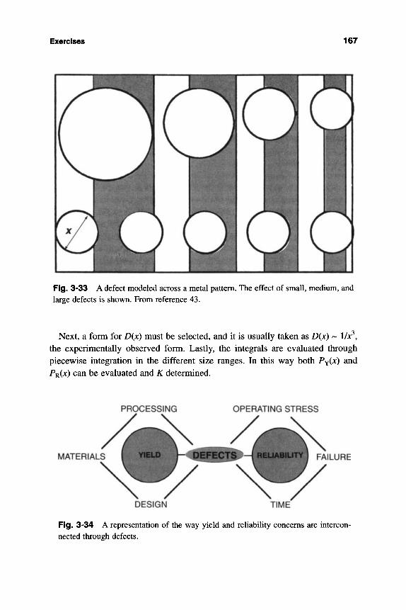
Exercises 167
Fig. 3-33 A defect modeled across a metal pattern. The effect of small, medium, and large defects is shown. From reference 43.
Next, a form for D(x) must be selected, and it is usually taken as D(x) -- l/x , the experimentally observed form. Lastly, the integrals are evaluated through piecewise integration in the different size ranges. In this way both PyW ^^^ PR(X) can be evaluated and K determined.
PROCESSING OPERATING STRESS
MATERIALS FAILURE
DESIGN TIME
Fig. 3-34 A representation of the way yield and reliability concerns are intercon-nected through defects.
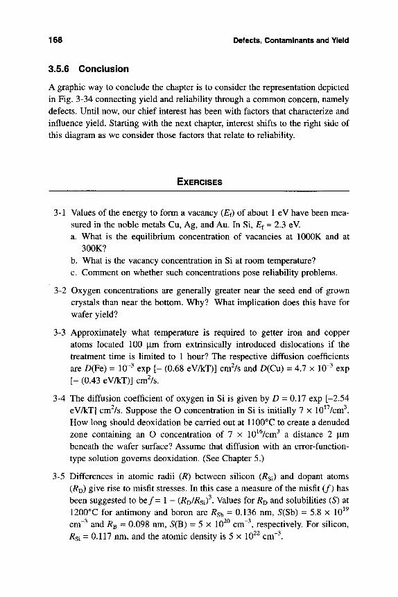
168 Defects, Contaminants and Yield
3.5.6 Conclusion
A graphic way to conclude the chapter is to consider the representation depicted in Fig. 3-34 connecting yield and reliability through a common concern, namely defects. Until now, our chief interest has been with factors that characterize and influence yield. Starting with the next chapter, interest shifts to the right side of this diagram as we consider those factors that relate to reliability.
EXERCISES
3-1 Values of the energy to form a vacancy (Ef) of about 1 eV have been mea-sured in the noble metals Cu, Ag, and Au. In Si, Ef ~ 2.3 eV. a. What is the equilibrium concentration of vacancies at lOOOK and at
300K? b. What is the vacancy concentration in Si at room temperature? c. Comment on whether such concentrations pose reliability problems.
3-2 Oxygen concentrations are generally greater near the seed end of grown crystals than near the bottom. Why? What implication does this have for wafer yield?
3-3 Approximately what temperature is required to getter iron and copper atoms located 100 |im from extrinsically introduced dislocations if the treatment time is limited to 1 hour? The respective diffusion coefficients are Z)(Fe) = 10"^ exp [- (0.68 eV/kT)] cm^/s and D(Cu) = 4.7 x 10"^ exp [- (0.43 eV/kT)] cm^/s.
3-4 The diffusion coefficient of oxygen in Si is given by Z) = 0.17 exp [-2.54 eV/kT] cm^/s. Suppose the O concentration in Si is initially 7 x 10^ /cm . How long should deoxidation be carried out at 1100°C to create a denuded zone containing an O concentration of 7 x 10^ /cm^ a distance 2 |a,m beneath the wafer surface? Assume that diffusion with an error-function-type solution governs deoxidation. (See Chapter 5.)
3-5 Differences in atomic radii (R) between silicon (/?si) and dopant atoms (Rjy) give rise to misfit stresses. In this case a measure of the misfit (/) has been suggested to b e / = 1 - (Rj^/Rsif. Values for J?D and solubilities (S) at 1200°C for antimony and boron are /?sb = 0.136 nm, 5(Sb) = 5.8 x 10^ cm~^ and R^ = 0.098 nm, 5(B) = 5 x 10^^ cm~ , respectively. For silicon, Rsi = 0.117 nm, and the atomic density is 5 x 10^^ cm~ .
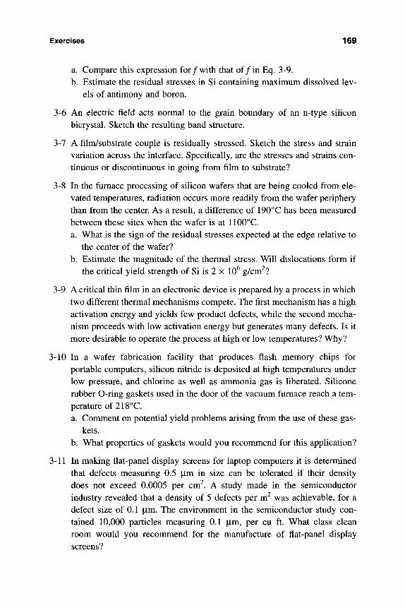
Exercises 169
a. Compare this expression for/with that of / in Eq. 3-9. b. Estimate the residual stresses in Si containing maximum dissolved lev-
els of antimony and boron.
3-6 An electric field acts normal to the grain boundary of an n-type silicon bicrystal. Sketch the resulting band structure.
3-7 A film/substrate couple is residually stressed. Sketch the stress and strain variation across the interface. Specifically, are the stresses and strains con-tinuous or discontinuous in going from film to substrate?
3-8 In the furnace processing of silicon wafers that are being cooled from ele-vated temperatures, radiation occurs more readily from the wafer periphery than from the center. As a result, a difference of 190°C has been measured between these sites when the wafer is at 1100°C. a. What is the sign of the residual stresses expected at the edge relative to
the center of the wafer? b. Estimate the magnitude of the thermal stress. Will dislocations form if
the critical yield strength of Si is 2 x 10^ g/cm^?
3-9 A critical thin film in an electronic device is prepared by a process in which two different thermal mechanisms compete. The first mechanism has a high activation energy and yields few product defects, while the second mecha-nism proceeds with low activation energy but generates many defects. Is it more desirable to operate the process at high or low temperatures? Why?
3-10 In a wafer fabrication facility that produces flash memory chips for portable computers, silicon nitride is deposited at high temperatures under low pressure, and chlorine as well as anmionia gas is liberated. Silicone rubber 0-ring gaskets used in the door of the vacuum furnace reach a tem-perature of 218 ° C. a. Comment on potential yield problems arising from the use of these gas-
kets. b. What properties of gaskets would you recommend for this application?
3-11 In making flat-panel display screens for laptop computers it is determined that defects measuring 0.5 |im in size can be tolerated if their density does not exceed 0.0005 per cm^. A study made in the semiconductor industry revealed that a density of 5 defects per m^ was achievable, for a defect size of 0.1 |Lim. The environment in the semiconductor study con-tained 10,000 particles measuring 0.1 |im, per cu ft. What class clean room would you recommend for the manufacture of flat-panel display screens?
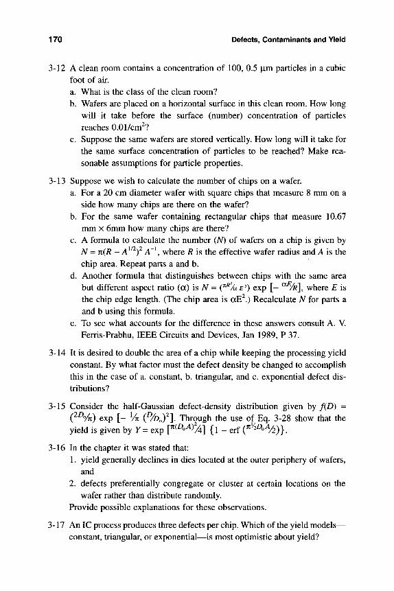
170 Defects, Contaminants and Yield
3-12 A clean room contains a concentration of 100, 0.5 |Lim particles in a cubic foot of air. a. What is the class of the clean room? b. Wafers are placed on a horizontal surface in this clean room. How long
will it take before the surface (number) concentration of particles reaches 0.01/cm^?
c. Suppose the same wafers are stored vertically. How long will it take for the same surface concentration of particles to be reached? Make rea-sonable assumptions for particle properties.
3-13 Suppose we wish to calculate the number of chips on a wafer. a. For a 20 cm diameter wafer with square chips that measure 8 mm on a
side how many chips are there on the wafer? b. For the same wafer containing rectangular chips that measure 10.67
mm X 6mm how many chips are there? c. A formula to calculate the number (AO of wafers on a chip is given by
A = n{R - A}'^i^ A~\ where R is the effective wafer radius and A is the chip area. Repeat parts a and b.
d. Another formula that distinguishes between chips with the same area but different aspect ratio (a) is A = i^^\ E^) exp [- ^R], where E is the chip edge length. (The chip area is aE^.) Recalculate A for parts a and b using this formula.
e. To see what accounts for the difference in these answers consult A. V. Ferris-Prabhu, IEEE Circuits and Devices, Jan 1989, P 37.
3-14 It is desired to double the area of a chip while keeping the processing yield constant. By what factor must the defect density be changed to accomplish this in the case of a. constant, b. triangular, and c. exponential defect dis-tributions?
3-15 Consider the half-Gaussian defect-density distribution given by f(D) = C^yn) exp [- VK ( % O ) ^ ] . Through the use of Eq. 3-28 show that the yield is given by y = exp [ < oA) / ] {j _ erf (^'^^oA/^^j
3-16 In the chapter it was stated that: 1. yield generally declines in dies located at the outer periphery of wafers,
and 2. defects preferentially congregate or cluster at certain locations on the
wafer rather than distribute randomly. Provide possible explanations for these observations.
3-17 An IC process produces three defects per chip. Which of the yield models— constant, triangular, or exponential—is most optimistic about yield?
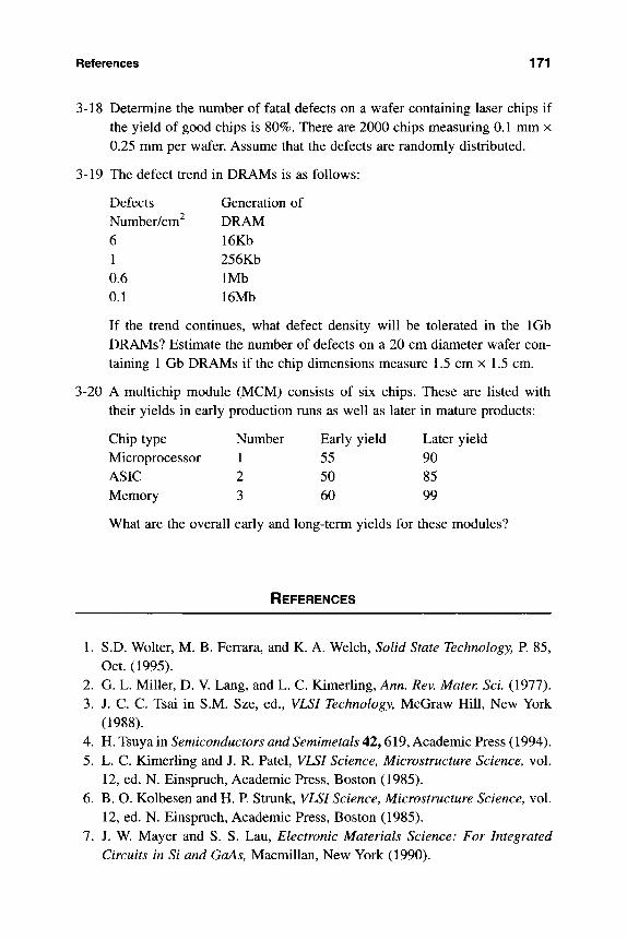
References 171
3-18 Determine the number of fatal defects on a wafer containing laser chips if the yield of good chips is 80%. There are 2000 chips measuring 0.1 mm x 0.25 mm per wafer. Assume that the defects are randomly distributed.
3-19 The defect trend in DRAMs is as follows:
Defects Number/cm^ 6 1 0.6 0.1
Generation of DRAM 16Kb 256Kb 1Mb 16Mb
If the trend continues, what defect density will be tolerated in the 1Gb DRAMs? Estimate the number of defects on a 20 cm diameter wafer con-taining 1 Gb DRAMs if the chip dimensions measure 1.5 cm x 1.5 cm.
3-20 A multichip module (MCM) consists of six chips. These are listed with their yields in early production runs as well as later in mature products:
Chip type Microprocessor ASIC Memory
Number 1 2 3
Early yield 55 50 60
Later yield 90 85 99
What are the overall early and long-term yields for these modules?
REFERENCES
1. S.D. Wolter, M. B. Ferrara, and K. A. Welch, Solid State Technology, R 85, Oct. (1995).
2. G. L. Miller, D. V. Lang, and L. C. Kimerling, Ann, Rev. Mater. Sci. (1977). 3. J. C. C. Tsai in S.M. Sze, ed., VLSI Technology, McGraw Hill, New York
(1988). 4. H. Tsuya in Semiconductors and Semimetals 42,619, Academic Press (1994). 5. L. C. Kimerling and J. R. Patel, VLSI Science, Microstructure Science, vol.
12, ed. N. Einspruch, Academic Press, Boston (1985). 6. B. O. Kolbesen and H. P. Strunk, VLSI Science, Microstructure Science, vol.
12, ed. N. Einspruch, Academic Press, Boston (1985). 7. J. W. Mayer and S. S. Lau, Electronic Materials Science: For Integrated
Circuits in Si and GaAs, Macmillan, New York (1990).

172 Defects, Contaminants and Yield
8. J. C. Zolper and A. M. Bamett, IEEE Trans. Elec. Dev. 37, 478 (1990). 9. S-H. Soh, J. Lari, S. Hunt, T. Davies, M. Kuo, U. Kim, M. Cheung, and E.
Lucero, 33rd Annual Proceedings of the IEEE Reliability Physics Sympo-sium, p. 244 (1995).
10. G. J. Declerck in Microelectronic Materials and Processing, ed. by R.A. Levy, Kluwer Academic Publ., Dordrecht (1989).
11. C.H. Seager, Ann. Rev. Mater Sci 15, 271 (1985). 12. P. M. Fahey, S. R. Mader, S. R. Stiffler, R. L. Mohler, J. D. Mis, and J. A.
Slinkman, IBM J. Res. and Develop. 36, 158 (1992). 13. B. O. Kolbesen, Crucial Issues in Semiconductor Materials and Processing
Technologies, ed. S. Coffa and J. M. Poate, Kluwer (1992). 14. G. L. Schnable in Microelectronics Manufacturing Diagnostics Handbook,
ed. A. H. Landsberg, Van Nostrand Reinhold, New York (1993). 15. I. Blech and D. Dang, Solid State Tech. 37 (8), 74 (1994). 16. M. Ohring, The Materials Science of Thin Films, Academic Press, Boston
(1992). 17. S. M. Hu, J. Appl. Phys. 70, R53 (1991). 18. T. T. Hitch, Circuit World 16 (2), (1990). 19. I. A. Blech, D. B. Fraser, and S. E. Hasko, J. Vac. ScL and Tech. 15.13 (1978). 20. W. D. Westwood, in Microelectronic Materials and Processes, esd. R. Levy,
Kluwer, Dordrecht (1989). 21. D. R. Cote, S. V. Nguyen, W. J. Cote, S. L. Pennington, A. K. Stamper, and
D. V. Podlesnik, IBM. J. Res. and Develop. 39, 437 (1995). 22. T. Hattori, Solid State Tech. 33, 7, S-1 (1990). 23. D. W. Cooper in Microelectronics Manufacturing Diagnostics Handbook,
ed. A. H. Landsberg, Van Nostrand Reinhold, New York (1993). 24. P Borden, IEEE Trans. Semiconductor Manuf 3 (4) 189 (1990). 25. P. Burggraaf, Semiconductor International 18 (5) 69 (1995). 26. F. A. Stevie, R. G. Wilson, D. S. Simons, M. I. Current, and P C. Zalm, /.
Vac. Sci. Technol, B 12 (4), 2263 (1994). 27. S. J. Fonash, C. R. Viswanathan, and Y. D. Chan, Solid State Tech, 37 (7),
99 (1994). 28. H. Shin and C. Hu, IEEE Trans. Semiconductor Manuf. 6, 96 (1993). 29. Y. Uraoka, K. Eriguchi, T. Tamaki and K. Tsuji, IEEE Trans. Semiconductor
Manuf 7, 293 (1994). 30. S. N. Gupta, A. K. Bagchi, and N. N. Kundu, Microelectronics Journal. 16
(1), 22 (1985). 31. S. Wolf and R. N. Tauber, Silicon Processing for the VLSI Era, Lattice
Press, Sunset Beach, CA (1986).
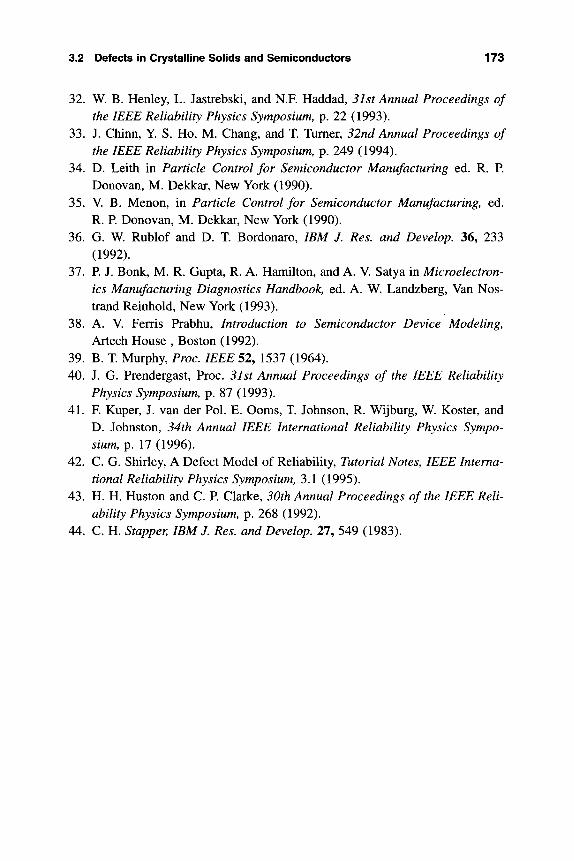
3.2 Defects in Crystalline Solids and Semiconductors 173
32. W. B. Henley, L. Jastrebski, and N.F. Haddad, 31st Annual Proceedings of the IEEE Reliability Physics Symposium, p. 22 (1993).
33. J. Chinn, Y. S. Ho, M. Chang, and T. Turner, 32nd Annual Proceedings of the IEEE Reliability Physics Symposium, p. 249 (1994).
34. D. Leith in Particle Control for Semiconductor Manufacturing ed. R. P. Donovan, M. Dekkar, New York (1990).
35. V. B. Menon, in Particle Control for Semiconductor Manufacturing, ed. R. R Donovan, M. Dekkar, New York (1990).
36. G. W. Rublof and D. T. Bordonaro, IBM J. Res. and Develop. 36, 233 (1992).
37. R J. Bonk, M. R. Gupta, R. A. Hamilton, and A. V. Satya in Microelectron-ics Manufacturing Diagnostics Handbook, ed. A. W. Landzberg, Van Nos-trand Reinhold, New York (1993).
38. A. V. Ferris Prabhu, Introduction to Semiconductor Device Modeling, Artech House , Boston (1992).
39. B. T. Murphy, Proc. IEEE 52, 1537 (1964). 40. J. G. Prendergast, Proc. 31st Annual Proceedings of the IEEE Reliability
Physics Symposium, p. 87 (1993). 41. F. Kuper, J. van der Pol. E. Ooms, T. Johnson, R. Wijburg, W. Koster, and
D. Johnston, 34th Annual IEEE International Reliability Physics Sympo-sium, p. 17 (1996).
42. C. G. Shirley, A Defect Model of Reliability, Tutorial Notes, IEEE Interna-tional Reliability Physics Symposium, 3.1 (1995).
43. H. H. Huston and C. P. Clarke, 30th Annual Proceedings of the IEEE Reli-ability Physics Symposium, p. 268 (1992).
44. C. H. Stapper, IBM J. Res. and Develop. 27, 549 (1983).

This Page Intentionally Left Blank
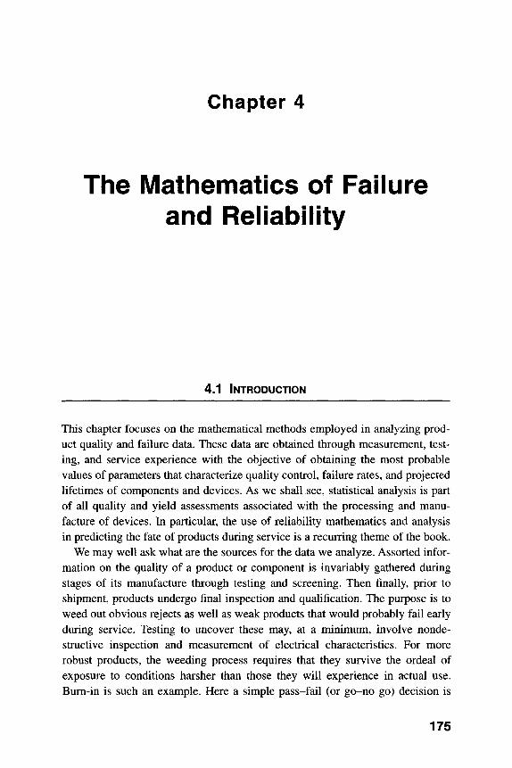
Chapter 4
The Mathematics of Failure and Reliability
4.1 INTRODUCTION
This chapter focuses on the mathematical methods employed in analyzing prod-uct quality and failure data. These data are obtained through measurement, test-ing, and service experience with the objective of obtaining the most probable values of parameters that characterize quality control, failure rates, and projected lifetimes of components and devices. As we shall see, statistical analysis is part of all quality and yield assessments associated with the processing and manu-facture of devices. In particular, the use of reliability mathematics and analysis in predicting the fate of products during service is a recurring theme of the book.
We may well ask what are the sources for the data we analyze. Assorted infor-mation on the quality of a product or component is invariably gathered during stages of its manufacture through testing and screening. Then finally, prior to shipment, products undergo final inspection and qualification. The purpose is to weed out obvious rejects as well as weak products that would probably fail early during service. Testing to uncover these may, at a minimum, involve nonde-structive inspection and measurement of electrical ch^acteristics. For more robust products, the weeding process requires that they survive the ordeal of exposure to conditions harsher than those they will experience in actual use. Bum-in is such an example. Here a simple pass-fail (or go-no go) decision is
175
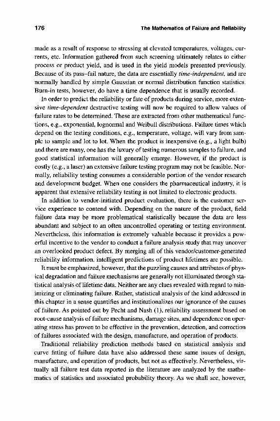
176 The Mathematics of Failure and Reliability
made as a result of response to stressing at elevated temperatures, voltages, cur-rents, etc. Information gathered from such screening ultimately relates to either process or product yield, and is used in the yield models presented previously. Because of its pass-fail nature, the data are essentially time-independent, and are normally handled by simple Gaussian or normal distribution function statistics. Bum-in tests, however, do have a time dependence that is usually recorded.
In order to predict the reliability or fate of products during service, more exten-sive time-dependent destructive testing will now be required to allow values of failure rates to be determined. These are extracted from other mathematical func-tions, e.g., exponential, lognormal and Weibull distributions. Failure times which depend on the testing conditions, e.g., temperature, voltage, will vary from sam-ple to sample and lot to lot. When the product is inexpensive (e.g., a light bulb) and there are many, one has the luxury of testing numerous samples to failure, and good statistical information will generally emerge. However, if the product is costly (e.g., a laser) an extensive failure testing program may not be feasible. Nor-mally, reliability testing consumes a considerable portion of the vendor research and development budget. When one considers the pharmaceutical industry, it is apparent that extensive reliability testing is not limited to electronic products.
In addition to vendor-initiated product evaluation, there is the customer ser-vice experience to contend with. Depending on the nature of the product, field failure data may be more problematical statistically because the data are less abundant and subject to an often uncontrolled operating or testing environment. Nevertheless, this information is extremely valuable because it provides a pow-erful incentive to the vendor to conduct a failure analysis study that may uncover an overlooked product defect. By merging all of this vendor/customer-generated reliability information, intelligent predictions of product lifetimes are possible.
It must be emphasized, however, that the puzzling causes and attributes of phys-ical degradation and failure mechanisms are generally not illuminated through sta-tistical analysis of lifetime data. Neither are any clues revealed with regard to min-imizing or eliminating failure. Rather, statistical analysis of the kind addressed in this chapter in a sense quantifies and institutionalizes our ignorance of the causes of failure. As pointed out by Pecht and Nash (1), reliability assessment based on root-cause analysis of failure mechanisms, damage sites, and dependence on oper-ating stress has proven to be effective in the prevention, detection, and correction of failures associated with the design, manufacture, and operation of products.
Traditional reliability prediction methods based on statistical analysis and curve fitting of failure data have also addressed these same issues of design, manufacture, and operation of products, but not as effectively. Nevertheless, vir-tually all failure test data reported in the literature are analyzed by the mathe-matics of statistics and associated probability theory. As we shall see, however.
4.2 Statistics and Definitions 177
there is controversy involved in doing this, and there are questions related to the credibility of the conclusions.
This chapter's discussion of statistics and probability, failure distributions, reliability estimates, and confidence of predictions is treated more extensively in the following references. They are recommended for their lucid presentations. P. A. Tobias and D. C. Tridade, Applied Reliability, Van Nostrand Reinhold, New York (1986). P. D. T. O'Connor, Practical Reliability Engineering, 2nd Ed., Wiley, Chichester (1986). F. R. Nash, Estimating Device Reliability: Assessment of Credibility, Kluwer Academic, Boston (1993). R. A. Evans, Tutorial Notes, Annual Reliability and Maintainability Sympos-ium (1994).
4.2 STATISTiCS AND DEFINITiONS
4.2.1 Normal Distribution Function
A useful skill for an engineer concerned with product reliability is to be able to convert a mass (mess?) of failure data into a form amenable to analysis without having a FIT. As an example, consider a company that makes electrical fuses for trucks that are rated at 10 amps. Fuses fail by melting when current-induced Joule heat cannot be effectively removed. Because fuses protect other circuitry from electrical overload failure, it is vital that they function within the rated value, say between 9 to 11 amps. Circuit damage or less than optimum performance may be the outcome of operating outside these current extremes. Fuses are produced in lots of tens of thousands, and it is not practical to test them all and reject those that fail. To determine if fuses operate within specifications without excessive vari-ability, a random population of fuses is chosen and tested by increasing the cur-rent until they fail or open circuit. The failure currents measured for such a popu-lation of 100 fuses are entered in Table 4-1. It is clear that although values cluster at about 10 amps, there is a spread that warrants further statistical analysis (2).
To proceed, it is convenient to first create a failure frequency distribution, as indicated in Table 4-2. For this purpose the range represented by minimum and maximum current values is arbitrarily subdivided into a number of cells (11 in this example) and the number of fuses destroyed in each current interval noted. The results are best represented in the form of a histogram, shown in Fig. 4-1, where the ordinate is the number (or percent) of failures. Since the histogram is approximately symmetric about 10 amps with only a ± 5% spread, the distribu-
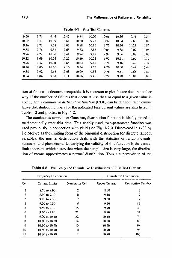
178 The Mathematics of Failure and Reliability
Table 4-1 Fuse Test Currents
9.60 10.22 9.46 9.58 9.76
10.12 9.76
10.20 9.88 8.84
9.76 10.41 9.72 9.76 9.22 9.69
10.32 10.06 9.92
10.04
9.46 10.19 9.28 9.51
10.01 10.24 10.04 10.36 9.56 9.88
10.42 9.61
10.02 9.68
10.44 10.23 9.88 9.16
10.08 10.11
9.34 10.20 9.88 9.82 9.74
10.89 10.02 9.54
10.09 10.06
10.20 9.76
10.11 8.86 9.88
10.22 9.62 9.76 9.58 9.46
10.06 10.32 9.72
10.04 9.92 9.92 9.76 9.20 9.76 9.72
10.36 10.04 10.24 9.88 9.56
10.21 9.46
10.00 9.51 9.28
9.16 9.88
10.24 10.09 10.08 9.60
10.42 10.44 9.68
10.02
9.54 10.02 10.85 10.06 10.08 10.19 9.34
10.48 9.82 9.89
tion of failures is deemed acceptable. It is common to plot failure data in another way. If the number of failures that occur at less than or equal to a given value is noted, then a cumulative distribution Junction (CDF) can be defined. Such cumu-lative distribution numbers for the indicated fuse current values are also Usted in Table 4-2 and plotted in Fig. 4-2.
The continuous normal, or Gaussian, distribution function is ideally suited to mathematically treat this data. This widely used, two-parameter function was used previously in connection with yield (see Fig. 3-26). Discovered in 1733 by De Moivre as the limiting form of the binomial distribution for discrete random variables, the normal distribution deals with the statistics of random events, numbers, and phenomena. Underlying the validity of this function is the central limit theorem, which states that when the sample size is very large, the distribu-tion of means approximates a normal distribution. Thus a superposition of the
Cell
1 2 3 4 5 6 7 8 9
10 11
Table 4-2 Frequency
Frequency Distribution
Current Limits
8.70 to 8.90 8.90 to 9.10 9.10 to 9.30 9.30 to 9.50 9.50 to 9.70 9.70 to 9.90 9.90 to 10.10
10.10 to 10.30 10.30 to 10.50 10.50 to 10.70 10.70 to 10.90
and Cumulative Distributions of Fuse Test Currents
Number in Cell
2 0 7 6
15 22 22 14 10 0 2
Cumulative Distribution
Upper Current
8.90 9.10 9.30 9.50 9.70 9.90
10.10 10.30 10.50 10.70 10.90
Cumulative Number
2 2 9
15 30 52 74 88 98 98
100
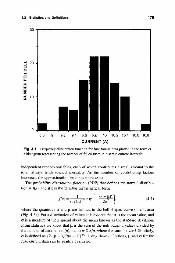
4.2 Statistics and Definitions 179
m o
lU
UJ
8.8 9 9.2 9.4 9.6 9.8 10 10.2 10.4 10.6 10.8
CURRENT (A)
Fig. 4-1 Frequency-distribution function for fuse failure data plotted in the form of a histogram representing the number of failed fuses in discrete current intervals.
independent random variables, each of which contributes a small amount to the total, always tends toward normality. As the number of contributing factors increases, the approximation becomes more exact.
The probability distribution function (PDF) that defines the normal distribu-tion is f(x), and it has the familiar mathematical form
f(x) = 1
a(27c) 172 exp 2c^ (4-1)
where the quantities a and |X are defined in the bell-shaped curve of unit area (Fig. 4-3a). For a distribution of values it is evident that |Li is the mean value, and a is a measure of their spread about the mean known as the standard deviation. From statistics we know that \i is the sum of the individual Xi values divided by the number of data points (n), i.e., |X = X Xf/n, where the sum is over /.Similarly, a is defined as {X [|i - xj^/(w - 1)}^^ . Using these definitions, |LI and a for the fuse current data can be readily evaluated.
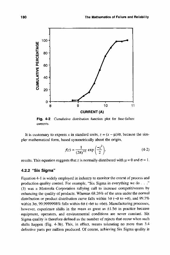
180 The Mathematics of Failure and Reliability
. 100-LU o < H g 80-O oc UJ 0- 60-UJ > H 3 40-3
s 3 ^ 20 -
f\ -u 1
^
^^ ' 1 ^^ 1 ^ 1 /
^ /
/ /
/ p
i 1 /
i M
_ /
1 • 1 • 1 • 3 9 10 1
CURRENT (A)
Fig. 4-2 Cumulative distribution function plot for fuse-failure currents.
It is customary to express x in standard units, z-{x- |Li)/a, because the sim-pler mathematical form, based symmetrically about the origin.
Az) = 1
(27C) 172" exp
-z 2
(4-2)
results. This equation suggests that z is normally distributed with |i = 0 and a = 1.
4,2,2 "Six Sigma"
Equation 4-1 is widely employed in industry to monitor the extent of process and production quality control. For example, "Six Sigma in everything we do . . ." (3) was a Motorola Corporation rallying call to increase competitiveness by enhancing the quality of products. Whereas 68.26% of the area under the normal distribution or product distribution curve falls within l a (-a to +a), and 99.7% within 3a, 99.9999998% falls within 6a (-6a to +6a). Manufacturing processes, however, experience shifts in the mean as great as ±1.5a in practice because equipment, operators, and environmental conditions are never constant. Six Sigma quality is therefore defined as the number of rejects that occur when such shifts happen (Fig. 4-3b). This, in effect, means tolerating no more than 3.4 defective parts per million produced. Of course, achieving Six Sigma quality is
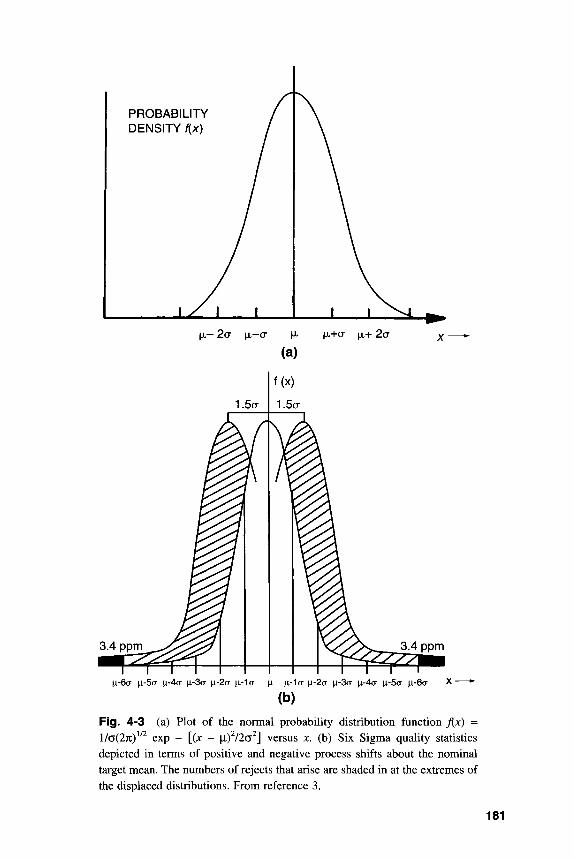
PROBABILITY DENSITY f(x)
p.-6a |j,-5a |i-4a |J,-3a |J.-2a [1-1G \i |j,-1o- p,-2a p.-3cT ^-4a p,-5(T \i-6(T
(b)
Fig. l/a(27c) ^^ exp
4-3 (a) Plot of the normal probability distribution function J{x) = [(x - \if/2o^] versus x. (b) Six Sigma quality statistics
depicted in terms of positive and negative process shifts about the nominal target mean. The numbers of rejects that arise are shaded in at the extremes of the displaced distributions. From reference 3.
181
182 The Mathematics of Failure and Reliability
easier said than done, but it remains a vital challenge for industry. Those inclined can calculate what seven sigma implies!
4.2.3 Accuracy and Precision
We have just seen that failure testing is subject to a Gaussian spread; the same is true of all property measurements and manufacturing quality control monitor-ing. With respect to measurements the most often asked questions are, How accurate are they, and with what precision are they made? The distinction between these two terms can be immediately grasped by viewing Fig. 4-4. High shooting accuracy is achieved in both Figs. 4-4a and b because the target hits are centered around the bull's-eye. Thus the mean value |X is the same in both cases and not far from the distribution center. But the precision of the shooter is better iij a than in b because all the bullet holes cluster and have a small dispersion, or spread. High precision is thus characterized by a small a; equivalently, we speak of a small random uncertainty. Poor accuracy is attained in Figs. 4-4c and d because all holes are far off the bull's-eye; here we speak of a large systematic uncertainty. Again, shooter precision is better in c because all the bullet holes cluster more tighdy. The case of Fig. 4-4d is worst of all because neither accu-racy nor precision is achieved; i.e., both a and |i are large.
Is it more desirable to have high accuracy or high precision? Good shooting instructors know that it is better first to work on attaining smaller clusters or groupings. Thus the path to becoming a sharpshooter is to be precise first. Accu-racy can then be gained by adjusting or calibrating the movable sights.
4.2.4 Failure Rates
The fuse current data treated above were essentially time independent. Reliabil-ity, however, implies time dependence of failure, with time reckoned from the instant the product is put into service. To include time (f) we first define the PDF to be/(0. Therefore, the CDF, defined by F{t), is given by the integral
F{t) = \'_^j\y)dy, ^ (4-3)
where the lower time limit is taken to be -oo instead of 0 for mathematical pur-poses, and J is a dummy variable of integration. For a given population. Fit) is the fraction that fails up to time t, and it is related to the PDF by/(0 = d F(t)ldt. A reliability, or survival, function, R{t), can then be defined to indicate the sur-viving fraction, i.e.,
R{t) = 1 - Fit). (4-4)
The failure rate (also known as ih^ hazard rate), Kit), is defined as the number of products (e.g., devices) that failed between t and t + At, per time increment At,
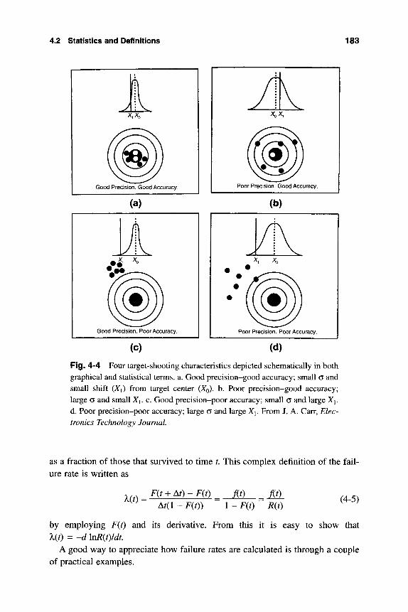
4.2 Statistics and Definitions 183
Fig. 4-4 Four target-shooting characteristics depicted schematically in both graphical and statistical terms, a. Good precision-good accuracy; small a and small shift (Xi) from target center (XQ). b. Poor precision-good accuracy; large a and small Xi. c. Good precision-poor accuracy; small o and large Xi. d. Poor precision-poor accuracy; large o and large Xj. From J. A. Carr, Elec-tronics Technology Journal.
as a fraction of those that survived to time t. This complex definition of the fail-ure rate is written as
m = F(t+M)-F(t)_ m _m At(l-F(t)) 1 - F ( 0 R(t)
(4-5)
by employing F(t) and its derivative. From this it is easy to show that Ut) = -d lnR(t)/dt.
A good way to appreciate how failure rates are calculated is through a couple of practical examples.
184 The Mathematics of Failure and Reliability
Example 4-1 Suppose that a population of 525,477 solid-state devices is burned in at elevated temperature, and the number of failed devices weeded out as a function of time is recorded in the following table. Determine the failure rates, X (t), at the indicated times.
Answer Results of the calculations are tabulated.
Time
(h)
Number Failed,/(O
Cumulative Failures, F(t)
Number of Device Hours FITS
1
2
3
4
5
6
7
8
9
10
6253
1034
617
419
502
401
297
214
206
193
6253
7287
7904
8323
8825
9226
9523
9737
9943
10136
0.0119
0.00199
0.00119
0.000810
0.000971
0.000777
0.000577
0.000415
0.000400
0.000375
525,477 X 1
519,224x2
518,190x3
517,573x4
517,154x5
516,652x6
516,252x7
515,954x8
515,740x9
515,534 X 10
1.19x10^
9.96 X 10^
3.97 X 10^
2.02 X 10^
1.94 X 10^
1.29 X 10^
8.22 X 10^
5.18 X 10^
4.44 X 10"
3.74 X 10^
Sample calculation at 5 h using Eq. 4-5: X (t) = 502/525,477 x (1 - 8323/525,477)"^ = 0.000971 h'^
Because the failure rates are very low, a new numerically larger unit, the FIT, has been defined and is widely used in the microelectronics industry. The FIT is not an acronym, but a contraction of "failure unit"; it equals the number of fail-ures in 10^ device-hours. For example, 1 FIT is 1 failure in 10^ devices after 100 hours of operation, or 1 failure in 10^ devices after 1000 hours, etc. Employing this definition, failure rates in terms of FITs were generated, and the values are displayed in the last column of the above table. After 5 hr, for example, X(t) = (502/517,154 X 5) X 10^ = 1.94 x 10^ FITs.
4.3 ALL ABOUT EXPONENTIAL, LOGNORMAL
AND WEIBULL DISTRIBUTIONS
4.3.1 Exponential Distribution Function
4.3,1,1 Mathematics We have already introduced the normal distribution function, whose PDF was given by Eq. 4-1. It was used to assess product prop-erties or quality, and no time dependence was attached to the variable of inter-est. There are three additional probability distribution functions, the exponential, lognormal, and Weibull, that can also be used like the normal distribution func-tion in evaluating quality control. But in this book they have a more vital role;
4.3 All About Exponential, Lognormal and Weibull Distributions 185
they are called upon to analyze and characterize failure and reliability data in material systems with the objective of predicting future behavior. Therefore, time and not a property relating to quality is now the variable of interest. Of these functions the most simple mathematically is the exponential distribution. The exponential probability distribution function is defined by
m = X, exp [- X, tl (4-6)
where ^o is a constant. Through simple integration (Eq. 4-2) the cumulative dis-tribution function is evaluated to be
F{t) = [ Xo exp [- X,y]dy=l- exp [- X, t]. (4-7)
Finally, the failure rate is given by
1 - F(t) [1 - (1 - exp - Xo t)]
and, importantly, is seen to be constant. Therefore, the mean time to failure (MTTF) is the reciprocal, or I/XQ. Plots of the functions f(t), F(t), and X(t) are depicted in Fig. 4-5 as a function of time (in l/X^ units).
Example 4-2 Suppose the population of devices is described by the life dis-tribution F(t) = 1 - exp [-0.000U]. a. What is the probability that a new device will fail after 1000 hr? After 5000 hr? Between these times? b. What is the failure rate at 1000 h? After 5000 h?
Answer a. By substitution, F{t) = 1 - exp [- 0.0001(1000)] = 0.095. Simi-larly, at 5000 h, F(t) = 0.39. The probability of device failure between 1000 and 5000 h is F(5000) - F(IOOO) = 0.39 - 0.095 = 0.30. b. fit) = dF(t)/dt = 0.0001 exp [-0.0001]. The failure rate is X(t) =f(t)/[l - F(t)] = 0.0001 exp [-0.000U]/exp [-O.OOOf] = 0.0001. For this distribution the failure rate is seen to be time-independent.
4.3.1.2 Constant Failure Rate Modeling Due to ease in dealing with a constant failure rate, the exponential distribution function has proven popular as the traditional basis for reliability modeling. For the reasons enumerated below, some of which are historical in nature, it is not difficult to see why the constant failure rate model has been so widely used (1).
1. The first generalized reliability models of the 1950s were based on electron vacuum tubes, and these exhibited constant failure rates.
2. Failure data acquired several decades ago were "tainted by equipment acci-dents, repair blunders, inadequate failure reporting, reporting of mixed age equipment, defective records of equipment operating times, mixed opera-
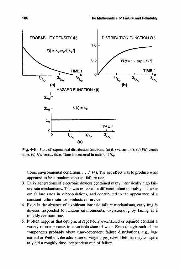
186 The Mathematics of Failure and Reliability
PROBABILITY DENSITY f{t)
f{t) = koexp[-kot]
TIMEf ! - • 0
DISTRIBUTION FUNCTION F{f)
K ^'K ^'K (a)
HAZARD FUNCTION \(t)
3Ko
0
X (0 = \o
TIMEf
"K ^IK 3/XO
(C)
Fig. 4-5 Plots of exponential distribution functions. (a)y(O versus time, (b) F(0 versus time, (c) X{t) versus time. Time is measured in units of XIX^,
tional environmental conditions . . ." (4). The net effect v as to produce what appeared to be a random constant failure rate.
3. Early generations of electronic devices contained many intrinsically high fail-ure rate mechanisms. This was reflected in different infant mortality and wear out failure rates in subpopulations, and contributed to the appearance of a constant failure rate for products in service.
4. Even in the absence of significant intrinsic failure mechanisms, early fragile devices responded to random environmental overstressing by failing at a roughly constant rate.
5. It often happens that equipment repeatedly overhauled or repaired contains a variety of components in a variable state of wear. Even though each of the components probably obeys time-dependent failure distributions, e.g., log-normal or WeibuU, the admixture of varying projected lifetimes may conspire to yield a roughly time-independent rate of failure.
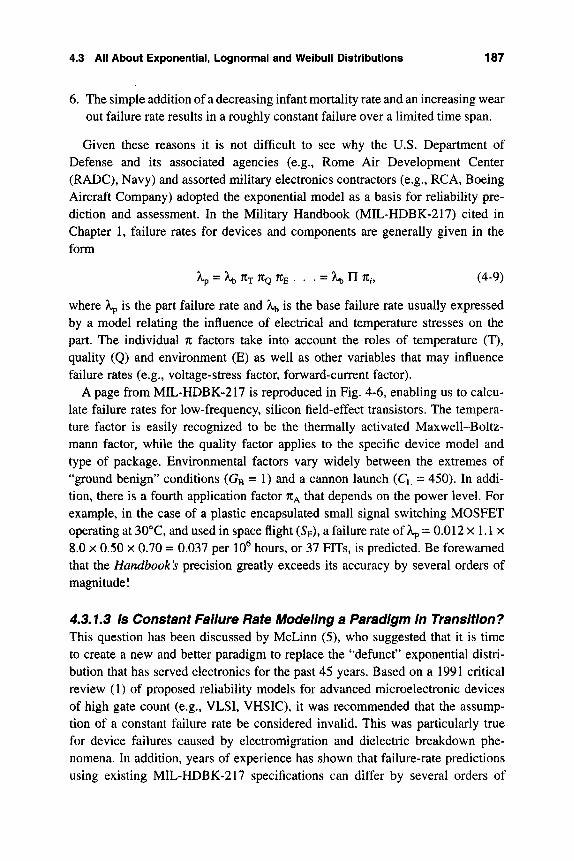
4.3 All About Exponential, Lognormal and Welbull Distributions 187
6. The simple addition of a decreasing infant mortality rate and an increasing wear out failure rate results in a roughly constant failure over a limited time span.
Given these reasons it is not difficult to see why the U.S. Department of Defense and its associated agencies (e.g., Rome Air Development Center (RADC), Navy) and assorted military electronics contractors (e.g., RCA, Boeing Aircraft Company) adopted the exponential model as a basis for reliability pre-diction and assessment. In the Military Handbook (MIL-HDBK-217) cited in Chapter 1, failure rates for devices and components are generally given in the form
5ip = A.b7CT^Q%' • .=X^nni, (4-9)
where Xp is the part failure rate and X^ is the base failure rate usually expressed by a model relating the influence of electrical and temperature stresses on the part. The individual n factors take into account the roles of temperature (T), quality (Q) and environment (E) as well as other variables that may influence failure rates (e.g., voltage-stress factor, forward-current factor).
A page from MIL-HDBK-217 is reproduced in Fig. 4-6, enabling us to calcu-late failure rates for low-frequency, silicon field-effect transistors. The tempera-ture factor is easily recognized to be the thermally activated Maxwell-Boltz-mann factor, while the quality factor applies to the specific device model and type of package. Environmental factors vary widely between the extremes of "ground benign'' conditions (GB = 1) and a cannon launch (CL = 450). In addi-tion, there is a fourth application factor n^, that depends on the power level. For example, in the case of a plastic encapsulated small signal switching MOSFET operating at 30®C, and used in space flight (Sp), a failure rate of X = 0.012 x 1.1 x 8.0 X 0.50 X 0.70 = 0.037 per 10^ hours, or 37 FITs, is predicted. Be forewarned that the Handbook's precision greatly exceeds its accuracy by several orders of magnitude!
4.3.f.3 Is Constant FailurB RatB Modeling a Paradigm In Transition? This question has been discussed by McLinn (5), who suggested that it is time to create a new and better paradigm to replace the "defuncf* exponential distri-bution that has served electronics for the past 45 years. Based on a 1991 critical review (1) of proposed reliability models for advanced microelectronic devices of high gate count (e.g., VLSI, VHSIC), it was recommended that the assump-tion of a constant failure rate be considered invalid. This was particularly true for device failures caused by electromigration and dielectric breakdown phe-nomena. In addition, years of experience has shown that failure-rate predictions using existing MIL-HDBK-217 specifications can differ by several orders of
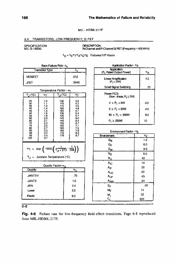
188 The Mathematics of Failure and Reliability
MIL- HDBK-217F
6.4 TRANSISTORS, LOW FREQUENCY, Si PET
SPECIFICATION MIL-S-19500
DESCRIPTION N-Channel and P-Channel Si FET (Frequency < 400 MHz)
^p = ^b' T' A' Q' E Failures/10^ Hours
Base Failure Rate -X Application Factor - TTA
MOSFET
JFET
1 ' .012
.0045
Temperature Factor - TTJ
1 Tj(°C) 25 30 35 40 45 50 55 60 65 70 75 80 85 90 95
100
n 1.0 1.1 1.2 1.4 1.5 1.6 1.8 2.0 2.1 2.3 2.5 2.7 3.0 3.2 3.4 3.7
TTj = exp / - 1 9 2 5 |
Tjro 105
1 110 115 120 125 130 135 140 145 150 155 160 165 170 175
f 1
n 1 3.9 4.2 4.5 4.8 5.1 5.4 5.7 6.0 6.4 6.7 7.1 7.5 7.9 8.3 8.7
1 \ \ T j + 273"298y^ 1
T j = Junction Temperature (°C)
Quality Factor-n-Q
1 Quality
JANTXV
JANTX
JAN
Lower
Plastic
- Q 1 .70
1.0
2.4
5.5
8.0
I Application 1 (Pp Rated Output Power)
Linear Amplification (Pr<2W)
1 Smell Signal Switching
Power FETs
(Non-linear, Pr>2W)
2 < P r < 5 W
5 < P r < 5 0 W 50 < Pr < 250W
Pr > 250W
1 1TA
1.5
.70
2.0
4.0
8.0
10
Environment Factor
1 Environment
GB
Gp
G M
Ns Nu
1 A|C A,F
Auc AuF
ARVV
1 " Mp
ML
1 CL 1
• ^ E
1 ^E 1 1.0 1
6.0
9.0
9.0
19
13
29
20
43
24
.50 1 14
32
320 1
6-8
Fig. 4-6 Failure rate for low-frequency field-effect transistors. Page 6-8 reproduced from MIL-HDBK-217F.
4.3 All About Exponential, Lognormal and Welbull Distributions 189
magnitude for the same device depending on manufacturer! Far from exhibiting a constant failure rate, it is well known that infant-mortality failures of semicon-ductor products display a decreasing failure rate with time. In addition, recent generations of semiconductor products are significantly more reliable than their predecessors and exhibit low failure rates.
To address these facts, MIL-HDBK-217 has incorporated additional terms such as the learning factor TCL, which attempts to weigh the effect of the number of years (Y) the product has been in production. One such explicit form is TCL = 0.01 exp (5.35 - 0.35Y). Inclusion of this time factor effectively results in a decreasing rather than constant hazard rate. Alternative constant failure-rate-reliability pre-diction procedures by various companies (e.g., AT&T, Bellcore, British Telecom, France Telecom, Nippon Telegraph and Telephone) have been developed. Finally, total abandonment of MIL-HDBK-217 specifications by some U.S. device man-ufacturers as well as by Japan and other Pacific Rim nations in favor of physical investigations of the root causes of failure has become increasingly popular.
In conclusion, two broad viewpoints of addressing reliability, MIL-HDBK-217 versus the physics of failure, are compared item by item in Table 4-3 to expose relative advantages and shortcomings.
4.3.2 Lognormal Distribution
Shortcomings in the exponential distribution function have prompted the use of alternative distribution functions to model reliability data. One of the most pop-ular of these is the lognormal distribution function. Mathematically, the lognor-mal is not a separate distribution, because by taking natural logarithms of all data points, the transformed data can be analyzed as a normal distribution. The lognormal PDF is given by
while the lognormal CDF has the form
Fit) = <E» a-Mn (4-11)
Here * (z) = i [1+ Erf (z/2"^)] or H 2 - Erfc (z/2"^)], since Erfc (z/2^'^) = 1 -Erf (z/2"^).
Substitution in Eq. 4-8 shows that the hazard function is given by
_ 2"^ exp[ - 1/2 o" {In (f/n)}^] ^ ' " n"^ t a Erfc [In (t/ii)/a (l/2)i'2-, • (4-1/)
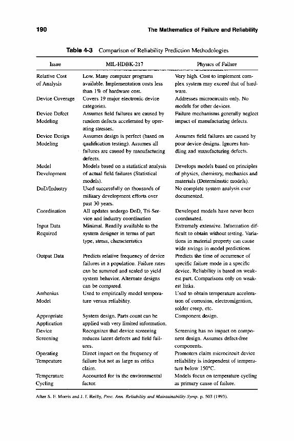
190 The Mathematics of Failure and Reliability
Table 4-3 Comparison of Reliability Prediction Methodologies
Issue MlL-HDBK-217 Physics of Failure
Relative Cost of Analysis
Device Coverage
Device Defect Modeling
Device Design Modeling
Model Development
DoD/Industry
Coordination
Input Data Required
Output Data
Low. Many computer programs available. Implementation costs less than 1% of hardware cost. Covers 19 major electronic device categories. Assumes field failures are caused by random defects accelerated by oper-ating stresses. Assumes design is perfect (based on qualification testing). Assumes all failures are caused by manufacturing defects. Models based on a statistical analysis of actual field failures (Statistical models). Used successfully on thousands of military development efforts over past 30 years. All updates undergo DoD, Tri-Ser-vice and industry coordination Minimal. Readily available to the system designer in terms of part type, stress, characteristics
Predicts relative frequency of device failures in a population. Failure rates can be summed and scaled to yield system behavior. Alternate designs can be compared.
Arrhenius Model
Appropriate Application Device Screening
Operating Tempeature
Temperature Cycling
Used to empirically model tempera-ture versus reliability.
System design. Parts count can be applied with very limited information. Recognizes that device screening reduces latent defects and field fail-ures. Direct impact on the frequency of failure but not as large as critics claim. Accounted for in the environmental factor.
Very high. Cost to implement com-plex system may exceed that of hard-ware. Addresses microcircuits only. No models for other devices. Failure mechanisms generally neglect impact of manufacturing defects.
Assumes field failures are caused by poor device designs. Ignores han-dling and manufacturing defects.
Develops models based on principles of physics, chemistry, mechanics and materials (Deterministic models). No complete system analysis ever documented.
Developed models have never been coordinated. Extremely extensive. Information dif-ficult to obtain without testing. Varia-tions in material property can cause wide swings in model predictions. Predicts the time of occurrence of specific failure mode in a specific device. Reliability is based on weak-est part. Comparisons only on weak-est hnks.
Used to obtain temperature accelera-tion of corrosion, electromigration, solder creep, etc. Component design.
Screening has no impact on compo-nent design. Assumes defect-free components. Promoters claim microcircuit device reliability is independent of tempera-ture below 150°C. Models focus on temperature cycling as primary cause of failure.
After S. F. Morris and J. f. Reilly, Proc. Ann. Reliability and Maintainability Symp. p. 503 (1993).
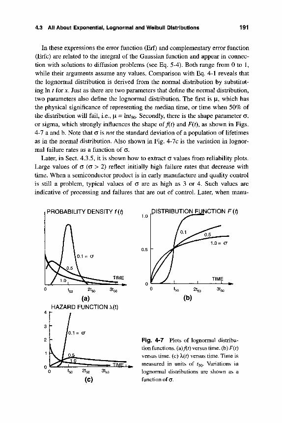
4.3 All About Exponential, Lognormal and Welbull Distributions 191
In these expressions the error function (Erf) and complementary error function (Erfc) are related to the integral of the Gaussian function and appear in connec-tion with solutions to diffusion problems (see Eq. 5-4). Both range from 0 to 1, while their arguments assume any values. Comparison with Eq. 4-1 reveals that the lognormal distribution is derived from the normal distribution by substitut-ing In t for X. Just as there are two parameters that define the normal distribution, two parameters also define the lognormal distribution. The first is |X, which has the physical significance of representing the median time, or time when 50% of the distribution will fail, i.e., |X = ln^5o. Secondly, there is the shape parameter a, or sigma, which strongly influences the shape of/(O and F{t), as shown in Figs. 4-7 a and b. Note that a is not the standard deviation of a population of lifetimes as in the normal distribution. Also shown in Fig. 4-7c is the variation in lognor-mal failure rates as a function of a.
Later, in Sect. 4.3.5, it is shown how to extract a values from reliability plots. Large values of a (a > 2) reflect initially high failure rates that decrease with time. When a semiconductor product is in early manufacture and quality control is still a problem, typical values of a are as high as 3 or 4. Such values are indicative of processing and failures that are out of control. Later, when manu-
PROBABILITY DENSITY f{f) DJSTRIBUTIOISJ FUNCTION F (ft
TIME
I50 ' ' '50
(a) HAZARD FUNCTION \(t)
Fig. 4-7 Plots of lognormal distribu-tion functions. (a)/(0 versus time, (b) F{t) versus time, (c) X{t) versus time. Time is measured in units of 50. Variations in lognormal distributions are shown as a function of a.
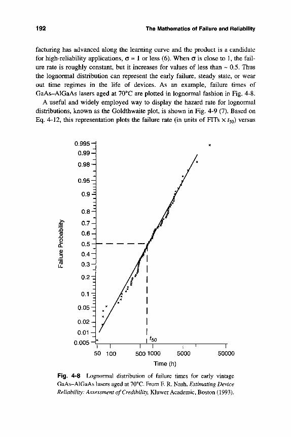
192 The Mathematics of Failure and Reliabiiity
facturing has advanced along the learning curve and the product is a candidate for high-reliability applications, a « 1 or less (6). When a is close to 1, the fail-ure rate is roughly constant, but it increases for values of less than ~ 0.5. Thus the lognormal distribution can represent the early failure, steady state, or wear out time regimes in the life of devices. As an example, failure times of GaAs-AlGaAs lasers aged at 70°C are plotted in lognormal fashion in Fig. 4-8.
A useful and widely employed way to display the hazard rate for lognormal distributions, known as the Goldthwaite plot, is shown in Fig. 4-9 (7). Based on Eq. 4-12, this representation plots the failure rate (in units of FITs x 50) versus
CO n 2 a.
CO
0.995-
0.99-
0 .98 -
0.95^
0.91
0 . 8 -
0 . 7 -
0 . 6 -
0 . 5 -
0 . 4 -
0 .3 -
0 . 2 -
0 . 1 ^
0.05":
0 .02-
0 . 0 1 -
0.005 —
X
H J
X /
X
1 r
/ X / X
/ X
/ x
/x
T"
*
ho 1
X
/ X
t/
^ r 50 100 5001000 5000
Time (h)
50000
Fig. 4-8 Lognormal distribution of failure times for early vintage GaAs-AlGaAs lasers aged at 70°C. From F. R. Nash, Estimating Device Reliability: Assessment of Credibility, Kluwer Academic, Boston (1993).
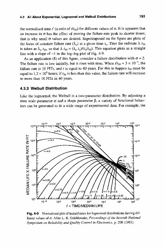
4.3 All About Exponential, Lognormal and Welbull Distributions 193
the normalized time t' (a ratio of tlt's^ for different values of a. It is apparent that an increase in a has the effect of moving the failure-rate peak to shorter times; that is why small a values are desired. Superimposed on the figure are plots of the locus of constant failure rate (A o) at a given time t^. Thus the ordinate X t^o is taken as X^ ho, so that X tso = (X^ Qlitjtso). This equation plots as a straight line with a slope of - 1 in the log-log plot of Fig. 4-9.
As an application (8) of this figure, consider a failure distribution with a = 2. The failure rate is low initially, but it rises with time. When tlt^Q ~ 3 x 10"^, the failure rate is 10 FITs, and t is equal to 40 years. For this to happen 50 must be equal to 1.2 x 10^ hours; if 50 is less than this value, the failure rate will increase to more than 10 FITs in 40 years.
4.3.3 Weibull Distribution
Like the lognormal, the Weibull is a two-parameter distribution. By adjusting a time scale parameter a and a shape parameter p, a variety of functional behav-iors can be generated to fit a wide range of experimental data. For example, the
10-10 10-10141 I I ||[ I I H[ I
10-6 10-4 10-2 100 102
I in| I iiij I ni| I I ii| I Mn I 111) I iru 014
10^0
10-10 10-8 10-6 10-4 10-2
f = TIME/MEDIAN LIFE
I Ml 1 till I i\\\l \ III i l l III I m l I III! 104
100 102
Fig. 4-9 Normalized plot of hazard rates for lognormal distributions having dif-ferent values of a. After L. R. Goldthwaite, Proceedings of the Seventh National Symposium on Reliability and Quality Control in Electronics, p. 208 (1961).
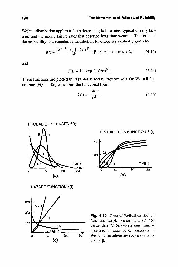
194 The Mathematics of Failure and Reliability
Weibull distribution applies to both decreasing failure rates, typical of early fail-ures, and increasing failure rates that describe long time wearout. The forms of the probability and cumulative distribution functions are explicitly given by
m = prP-^expKt /g)^]
a^ (P, a are constants > 0) (4-13)
and
F (0= l - e x p [ - ( t / a ) P ] . (4-14)
These functions are plotted in Figs. 4-10a and b, together with the Weibull fail-ure-rate (Fig. 4-lOc) which has the functional form
- . (4-15) X<0 = ^ a^
PROBABILITY DENSITY f (t)
DISTRIBUTION FUNCTION F (t)
HAZARD FUNCTION X(t)
3/a
2/a Fig. 4-10 Plots of Weibull distribution functions, (a) j{t) versus time, (b) F{t) versus time, (c) X{t) versus time. Time is measured in units of a. Variations in Weibull distributions are shown as a func-tion of p.
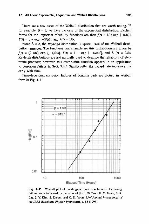
4.3 All About Exponential, Lognormal and Weibull Distributions 195
There are a few cases of the Weibull distribution that are worth noting. If, for example, (3 = 1, we have the case of the exponential distribution. Explicit forms for the important reliability functions are then J{t) = 1/a exp [-(t/a)]y F(t) = 1 - exp hO/a)], and X(0 = 1/a.
When p = 2, the Rayleigh distribution, a special case of the Weibull distri-bution, emerges. The functions that characterize this distribution are given by M = (2 t/a) exp h (t/a)l F{t) = 1 - exp [- {t/afl and X (t) = 2f/a. Rayleigh distributions are not normally used to describe the reliability of elec-tronic products; however, this distribution function appears in an application to corrosion failure in Sect. 7.4.4 Significantly, the hazard rate increases lin-early with time.
Time-dependent corrosion failures of bonding pads are plotted in Weibull form in Fig. 4-11.
§5 0.1 I
0.01
1 ! liiXil* i.59fii:lTt^"^
a = 812.1|~.~4-M- '
.tiiiti •.n4n..n j |,..l„.|.,4. J., j ^ ..|
10 100
Elapsed Time (Hours)
1000
Fig. 4-11 Weibull plot of bonding-pad coirosion failures. Increasing failure rate is indicated by the value of p = 1.59. From K. D. Hong, S. S. Lee, J. Y. Kim, S. Daniel, and C. K. Yoon, 33rd Annual Proceedings of the IEEE Reliability Physics Symposium, p. 85 (1995).
196 The Mathematics of Failure and Reliability
4.3.4 Lognormal versus Weibull
A comparative examination of Figs. 4-7 and 4-10 reveals that the PDF, CDF, and failure rates of both of these important functions can be made to approximate one another by adjusting the respective parameters. If this is the case, then what are the distinctions among these distributions? Does it make a difference which function is chosen to describe failure data? Which failure phenomena are best plotted in lognormal form and which are better described by a Weibull distribu-tion? And finally, do these functions have any physical significance? This last question, which underlies the previous three, is addressed separately in Sect. 4.5.
Which distribution to use for a given set of data is an important question in reliability modeling. Both lognormal and Weibull distributions outwardly appear to fit most sets of data equally, as illustrated in Fig. 4-12 for the case of light bulb wear-out failures (9). Closer examination, however, reveals that the Weibull distribution provides a better fit to short time failures, while the lognormal plot is better at predicting longer lifetimes. However, in this application long-time projections rather than infant-mortality failures are usually of interest; thus a lognormal characterization of bulb life is preferred.
Lognormal distributions tend to apply when gradual degradation occurs over time because of diffusion effects, corrosion processes, and chemical reactions. Early p-n-p mesa transistors, bipolar and MOS transistors, light-emitting diodes, and lasers are examples of devices whose failures have been modeled by lognormal statistics (10). On the other hand, Weibull distributions appear to be applicable in cases where the weak link, or the first of many flaws, propagates to failure. Dielectric breakdown, capacitor failures, and fracture in ceramics are typically described by Weibull distributions.
Plotting failure data that fit lognormal and Weibull distributions is facilitated with the use of special lognormal or Weibull graph paper because the desired lin-ear plots result. When predictions must be projected beyond the range of recorded failure data, the choice of the distribution function becomes important. A more advanced knowledge of statistics, probability theory, and failure physics may be required to make intelligent life projections in such cases.
4.3.5 Plotting Probability Functions as Straight Lines
Virtually every reliability study concludes with some sort of linear plot of the number of failures versus time from which reliability parameters are derived. Just what constitutes the failed population, or a quantity equivalent to or propor-tional to it, depends on the particular failure phenomenon in question. The rate of current increase is such a measure for laser failures in Fig. 4-8. Since a good linear fit of failure time data is required, the question arises of how to make non-
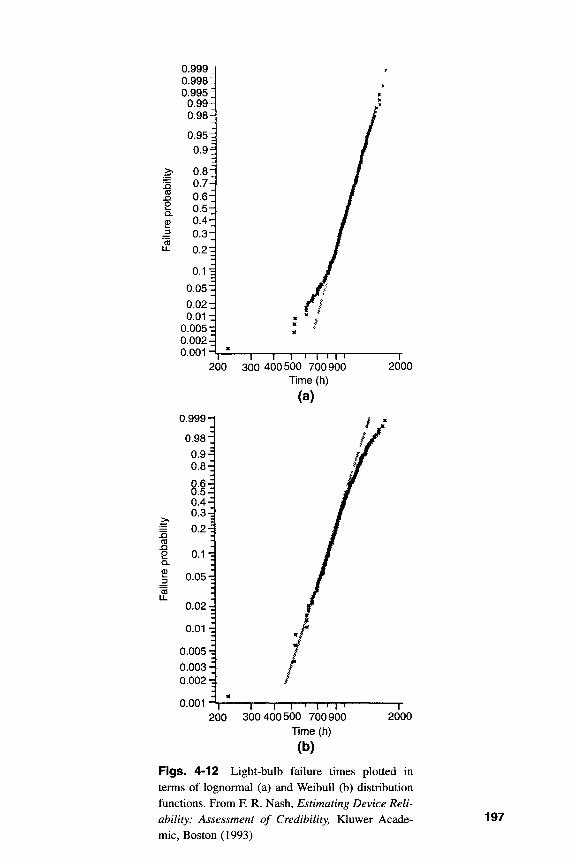
CO
2 Q.
'cO
0.9991 0.998 0.995
0.99 0.98 0.95^ 0.9
0.8^ 0.7 0.6 0.5d 0.4 0 . 3 i 0.2
0.1" 0.05" 0.02-0.01
0.005 0.002. 0.001 • 1—
200
0.999-
0.98-0.9-0.8-
0.4-0.3-
I 0.. CO JD O Q.
_g 'cO LL
0.1-
0.05-
0.02-J
0.01 d
0.0051 0.003-H 0.002 -d
0.001
— I 1—I I I I I I 300 400500 700900
Time (h)
(a)
2000
2000 1 \ — I I I I I I
200 300 400500 700900
Time (li)
(b)
Figs. 4-12 Light-bulb failure times plotted in terms of lognormal (a) and WeibuU (b) distribution functions. From F. R. Nash, Estimating Device Reli-ability: Assessment of Credibility, Kluwer Acade-mic, Boston (1993)
197
198 The Mathematics of Failure and Reliability
linear reliability functions plot as straight lines. Equivalently, how are Weibull and lognormal plot axes created so that lines emerge when plotting failure-statistics data versus time? Reliability analysis is then essentially reduced to selecting the right plotting paper or computer program that generates it.
The problem of linearizing the Weibull function is easy because no complex functions are involved. Starting with Eq. 4-14 we note that taking successive logs of both sides yields
\n[l-F(t)]=-(t/af (4-16)
and
hi{-ln [1 - F(t)]} = p In (0 - P In a. (4-17)
The simple algebraic equation of a straight line is y = mx-\-b, where y is the ordi-nate, X is the abscissa, m is equal to the slope, and b represents the intercept on the ordinate axis. In comparison with Eq. 4-17, y = ln{-ln [1 - F(0]}, x = \n (t), m = P, and ^ = - p In a. Thus Weibull paper is generated by plotting In {-In [1 - F(t)]} or log {-log [1 - F(t)]} usually expressed as cumulative percentage, versus either ln(0 or log(0, respectively. If the CDF or F(t) data that ranges from slightly above zero to slightly below 1.0 obeys Weibull statistics as a function of time, then a straight line will be obtained when plotted on this paper. It is not a difficult matter to extract p and a values using standard algebraic methods.
In the case of the lognormal function, Eq. 4-11 suggests that a straight line results if In t is plotted versus Q>~^F(t); i.e.. In r = |Li + a O"^F(0. From this plot a slope of a and an intercept equal to [i are obtained. The slope can also be esti-mated from the literal definition
In t2 - In ti ^~'F(t2) - 0-^F(/i) * c^=^-ir^ Z^U.' (4-18)
This last expression simplifies if points on the graph corresponding to F = 50%, 50% and F = 15.9%, 15.9% are selected. Letting 0"*F(/2) = 0, F(t2) = O (0), and
therefore F(t2) = 0.5; similarly ^~^F(ti) = -1.00 when F(ti) = 0 ( - l ) = 0.159. (Note Erf (-z) = -Erf (z).) Substituting these values yields the simple result a = In [ 0.5/ .159]- For example, in the case of Fig. 4-8, a = 1.1.
When failure data are abundant and there are many F values to plot, little dif-ficulty in generating straight lines is experienced. However, what if there are few failures, so that obtaining a good estimate of statistical parameters is problemat-ical? Under these circumstances F can be obtained by ranking the exact failure times. For example, if the sample size is n, then l/n is an estimate of F(t) for the first ordered failure time, 2/n for the second failure time, etc. Thus, for the ith failure, F(ti) = /M.There is, however, a recommended way to estimate a statisti-
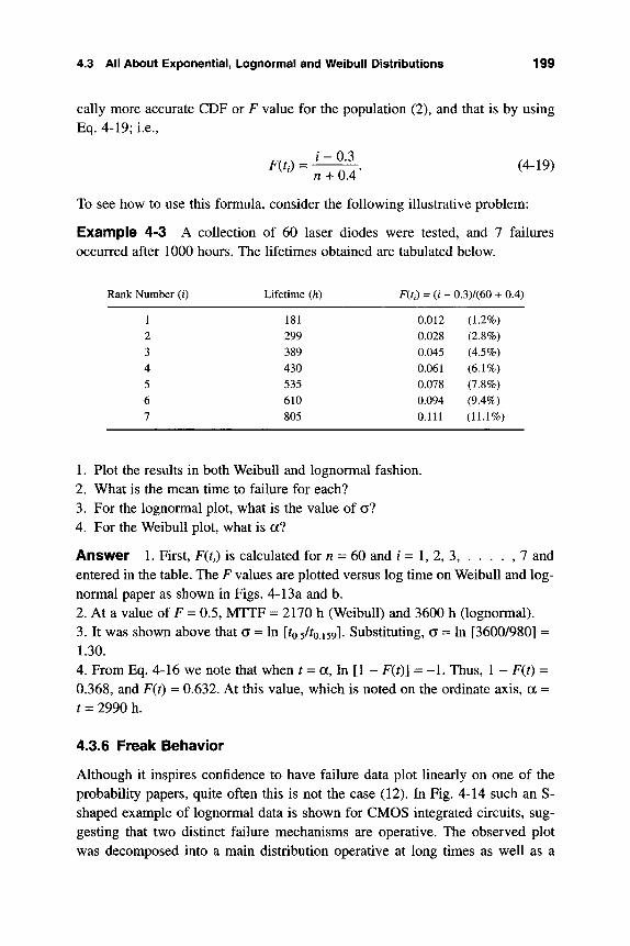
4.3 All About Exponential, Lognormal and Weibull Distributions 199
cally more accurate CDF or F value for the population (2), and that is by using Eq. 4-19; i.e.,
To see how to use this formula, consider the following illustrative problem:
Example 4-3 A collection of 60 laser diodes were tested, and 7 failures occurred after 1000 hours. The lifetimes obtained are tabulated below.
Rank Number (0
1 2 3 4 5 6 7
Lifetime (h)
181 299 389 430 535 610 805
Fitd = a -
0.012 0.028 0.045 0.061 0.078 0.094 0.111
0.3)/(60 + 0.4)
(1.2%) (2.8%) (4.5%) (6.1%) (7.8%) (9.4%) (11.1%)
1. Plot the results in both Weibull and lognormal fashion. 2. What is the mean time to failure for each? 3. For the lognormal plot, what is the value of a? 4. For the Weibull plot, what is a?
Answer 1. First, F(ti) is calculated for n = 60 and / = 1, 2, 3, . . . . , 7 and entered in the table. The F values are plotted versus log time on Weibull and log-normal paper as shown in Figs. 4-13a and b. 2. At a value of F = 0.5, MTTF = 2170 h (Weibull) and 3600 h (lognormal). 3. It was shown above that a = In [^.5/^.159]. Substituting, a = In [3600/980] = 1.30. 4. From Eq. 4-16 we note that when r = a. In [1 - F(t)] = - 1 . Thus, 1 - F(t) = 0.368, and F{t) = 0.632. At this value, which is noted on the ordinate axis, a = t = 2990 h.
4.3.6 Freak Behavior
Although it inspires confidence to have failure data plot linearly on one of the probability papers, quite often this is not the case (12). In Fig. 4-14 such an S-shaped example of lognormal data is shown for CMOS integrated circuits, sug-gesting that two distinct failure mechanisms are operative. The observed plot was decomposed into a main distribution operative at long times as well as a
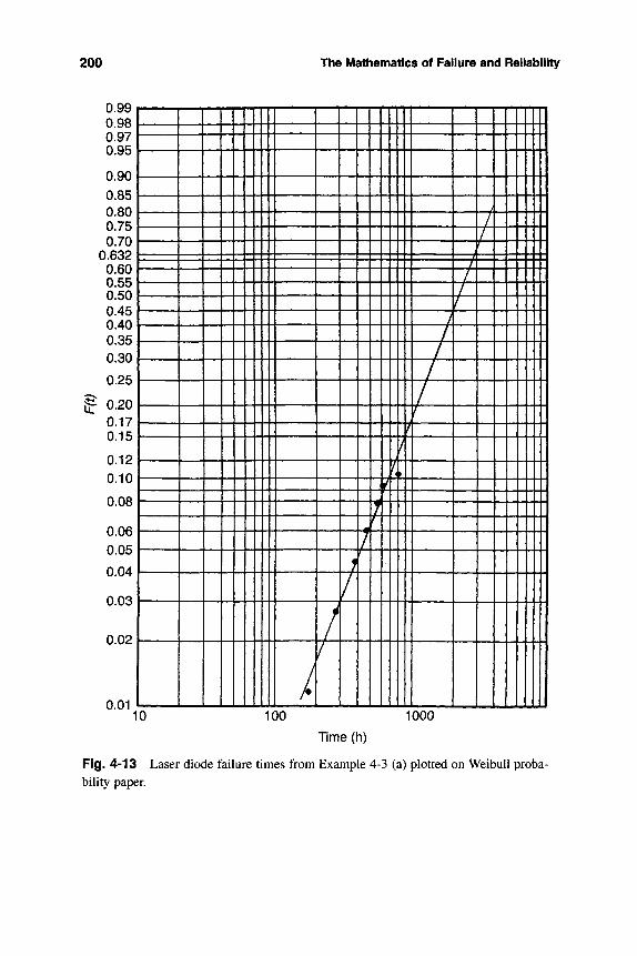
200 The Mathematics of Failure and Reliability
0.99 0.98 0.97 0.95
0.90 0.85 0.80 0.75 0.70
0.632 0.60 0.55 0.50 0.45 0.40 0.35 0.30
0.25
' 0.20 0.17 0.15
0.12 0.10
0.08
0.06 0.05 0.04
0.03
0.02
0.01 JIL
_ _ i _ i i _
IT7 m
vl J
v\\ All /
/ /
/
/ w /
m m r ^llll
A M N Y 4
/ /
10 100 1000
Time (h)
Fig. 4-13 Laser diode failure times from Example 4-3 (a) plotted on Weibull proba-bility paper.
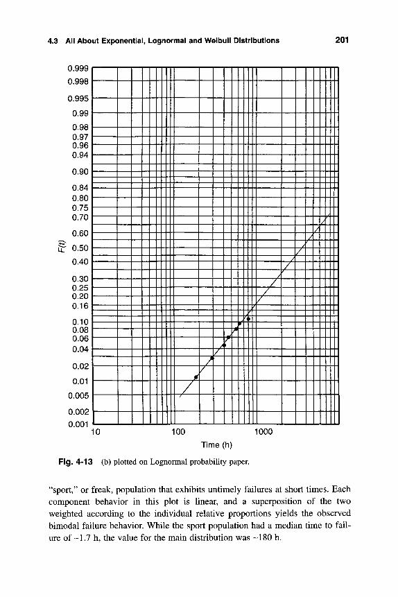
4.3 All About Exponential, Lognormal and Weibull Distributions 201
0.999
0.998
0.995
0.99
0.98 0.97 0.96 0.94
0.90
0.84 0.80 0.75 0.70
0.60
§^ 0.50
0.40
0.30 0.25 0.20 0.16
0.10 0.08 0.06 0.04
0.02
0.01
0.005
0.002
0.001 10 100 1000
Time (h)
Fig. 4-13 (b) plotted on Lognormal probability paper.
*
/ /
/ /
1 1 1 F
1
/ /
/ 1111/ 1 1 y] 1 A\ I i t
/ / ^
" ~ ~ T ~ r i — V \ 1
1 MINI M 11 III K 1
4 1 1 iiJ
"sport," or freak, population that exhibits untimely failures at short times. Each component behavior in this plot is linear, and a superposition of the two weighted according to the individual relative proportions yields the observed bimodal failure behavior. While the sport population had a median time to fail-ure of -1.7 h, the value for the main distribution was -180 h.
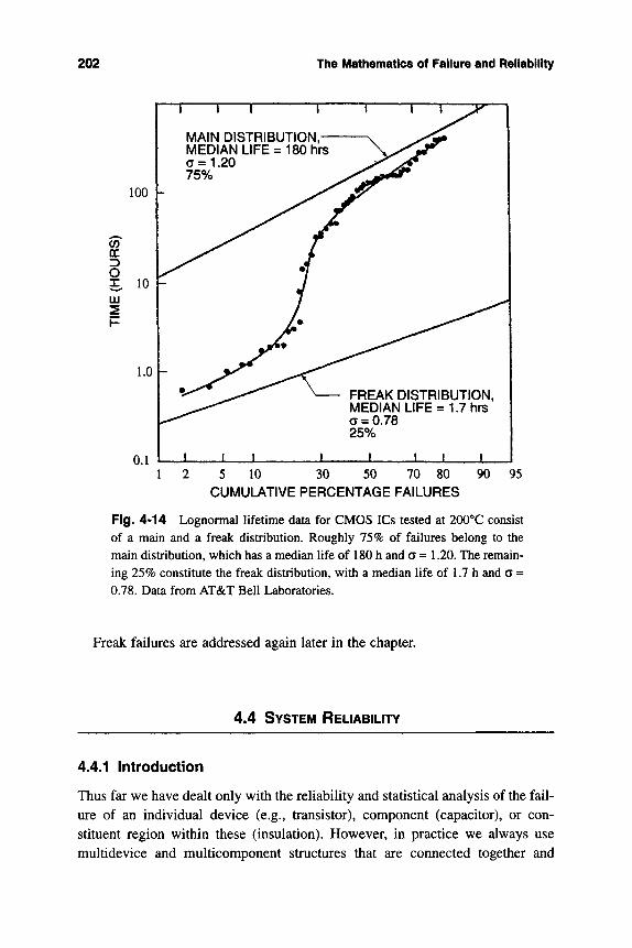
202 The Mathematics of Failure and Reliability
100
CO CL
o LU
T — r
0.1
IVIAIN DISTRIBUTION,-MEDIAN LIFE = 180 hrs a = 1.20 75%
FREAK DISTRIBUTION. MEDIAN LIFE = 1.7 hrs a = 0.78 25%
_L JL JL J - X -L I
5 10 30 50 70 80 CUMULATIVE PERCENTAGE FAILURES
90 95
Fig. 4-14 Lognormal lifetime data for CMOS ICs tested at 200'*C consist of a main and a freak distribution. Roughly 75% of failures belong to the main distribution, which has a median life of 180 h and c = 1.20. The remain-ing 25% constitute the freak distribution, with a median life of 1.7 h and a = 0.78. Data from AT&T Bell Laboratories.
Freak failures are addressed again later in the chapter.
4.4 SYSTEM RELIABILITY
4.4.1 Introduction
Thus far we have dealt only with the reliability and statistical analysis of the fail-ure of an individual device (e.g., transistor), component (capacitor), or con-stituent region within these (insulation). However, in practice we always use multidevice and multicomponent structures that are connected together and
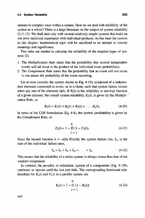
4.4 System Reliability 203
interact in complex ways within a system. How do we deal with reliability of the system as a whole? There is a large literature on the subject of system reliability (2,11,13). We shall deal only with several relatively simple systems that build on our prior statistical experience with individual products. As has been the custom in this chapter, mathematical rigor will be sacrificed in an attempt to convey meanings and significance.
Two rules are needed to calculate the reliability of the simplest types of sys-tems (2).
1. The Multiplication Rule states that the probability that several independent events will all occur is the product of the individual event probabilities.
2. The Complement Rule states that the probability that an event will not occur is one minus the probability of the event occurring.
Let us now consider the system shown in Fig. 4-15a composed of n indepen-dent elements connected in series, or in a chain, such that system failure occurs when any one of the elements fails. If R^t) is the reliability or survival function of a given element, the overall system reliability, R^it), is given by the Multipli-' cation Rule, or
RM = Ri(t) X R2(t) X R^(t) X , . . RM (4-20)
In terms of the CDF formulation (Eq. 4-4), the system unreliability is given by the Complement Rule, or
n F , ( 0 = l - n ( l - F , ( 0 ) . (4-21)
1 = 1
Since the hazard function X = -d[ln R{t)ydt, the system failure rate, X^, is the sum of the individual failure rates,
Xs = Xi + X2 + X.3'f . . . + V (4-22)
This means that the reliability of a series system is always worse than that of the weakest component.
In contrast, AQ parallel or redundant, system of n components (Fig. 4-15b) continues to operate until the last unit fails. The corresponding functional rela-tionships for R^(t) and F^(t) in a parallel system are
n RM=l-n[l^Rm (4-23)
i=l
and
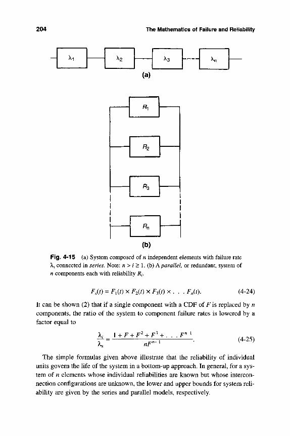
204 The Mathematics of Failure and Reliability
H 1 X2
(a)
fln
3
(b)
Fig. 4-15 (a) System composed of n independent elements with failure rate Xi connected in series. Note: « > / > 1. (b) A parallel, or redundant, system of n components each with reliability /?,.
^s(0 = F,(t) X F2(t) X F,(t) X . . . FM (4-24)
It can be shown (2) that if a single component with a CDF of F is replaced by n components, the ratio of the system to component failure rates is lowered by a factor equal to
1 + F + F^ + F^ + , .F" nF""
(4-25)
The simple formulas given above illustrate that the reliability of individual units govern the life of the system in a bottom-up approach. In general, for a sys-tem of n elements whose individual reliabilities are known but whose intercon-nection configurations are unknown, the lower and upper bounds for system reli-ability are given by the series and parallel models, respectively.
4.4 System Reliability 205
Example 4-4 Consider a 50 pin module such that the probabihty of failure upon inserting it into a mating connector is 1.8 x 10~^% per pin. What is the probability of failure of the module?
Answer In this problem the module is the system (s), and the pins (p) are the elements. If we assume that a single pin failure causes the module to fail, then by Eq. 4-21, Fs = 1 - (1 - Fp)", where n is the number of pins per module. Sub-stituting, Fp = 1.8 X 10"^ and n = 50 yields F^ = 1 - (1 - 1.8 x 10" ) ^ = 0.00090.
Therefore, the failure probability is predicted to be 0.09%, or 9 module fail-ures in 10,000 insertions.
4.4.2 Redundancy in a Two-Laser System
Transoceanic cables for optical communications systems typically contain a hundred or so repeaters stretched across the ocean floor. Their function is to boost, or regenerate, the laser light signal, which attenuates with distance of transmission. Because of the enormous expense of submarine cable repair, redundant lasers are used in repeater systems to achieve the high reliability that is so critical in this application. Redundancy, or the presence of spares that can be pressed into service should they be needed, is a common strategy used to achieve low system failure rates. In this section we consider the reli-ability of a regenerator that contains two lasers, one sparing the other, where each is assumed to fail according to lognormal statistics. Joyce and Anthony (6) considered two different models for the two-laser regenerator, and they are treated in turn:
a. Cold-Spared Assembly In the so-called "cold-spared" assembly the second laser is called into service and begins to degrade after the first laser fails. The duration of system survival depends on the first component lasting until turn-on of the second, and the probability that the second will operate to time t. A plot of the cold spared failure rate, X^ (c), is shown Fig. 4-16, and clearly resembles the Goldthwaite plot (Fig. 4-9).
As an example, let us assume the lasers have a median lifetime of 100 years and a = 1. After 10 years of system life, the abscissa of Fig. 4-16 is 10~\ in which case X, (c) (FITs) x /50 = 3 x 10^ Therefore, X, (c) = 3 x 10^/8.76 x 10^ = 0.34 FITs. With the passage of time the advantages of redundancy diminish.
b. Hot-Spared (Parallel) Assembly This assembly consists of lasers con-figured in parallel. Thus, lasers degrade concurrently, and the assembly fails if and only if both independent components fail. For this simpler case, the appro-priate lognormal distribution and hazard functions of Equations 4-11 and 12
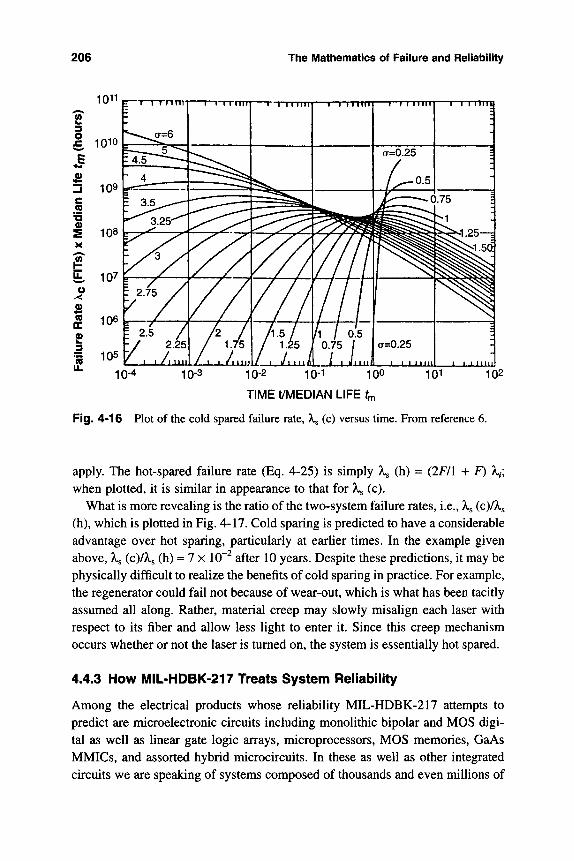
206 The Mathematics of Failure and Reliability
1011 rr
3 O
J & '3 c
(0
X
5? o
3
TIME t/MEDIAN LIFE f
Fig. 4-16 Plot of the cold spared failure rate, X^ (c) versus time. From reference 6.
apply. The hot-spared failure rate (Eq. 4-25) is simply X^ (h) = (2F/1 + F) Xf, when plotted, it is similar in appearance to that for X^ (c).
What is more revealing is the ratio of the two-system failure rates, i.e., X^ (c)/Xs (h), which is plotted in Fig. 4-17. Cold sparing is predicted to have a considerable advantage over hot sparing, particularly at earlier times. In the example given above, X^ (c)/Xs (h) = 7 x 10"^ after 10 years. Despite these predictions, it may be physically difficult to realize the benefits of cold sparing in practice. For example, the regenerator could fail not because of wear-out, which is what has been tacitly assumed all along. Rather, material creep may slowly misalign each laser with respect to its fiber and allow less light to enter it. Since this creep mechanism occurs whether or not the laser is turned on, the system is essentially hot spared.
4.4.3 How MIL-HDBK-217 Treats System Reliability
Among the electrical products whose reliability MIL-HDBK-217 attempts to predict are microelectronic circuits including monolithic bipolar and MOS digi-tal as well as linear gate logic arrays, microprocessors, MOS memories, GaAs MMICs, and assorted hybrid microcircuits. In these as well as other integrated circuits we are speaking of systems composed of thousands and even millions of
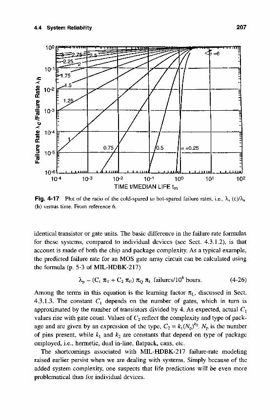
4.4 System Reliability 207
TIME t/MEDIAN LIFE tm
Fig. 4-17 Plot of the ratio of the cold-spared to hot-spared failure rates, i.e., X^ (c)/Xs (h) versus time. From reference 6.
identical transistor or gate units. The basic difference in the failure rate formulas for these systems, compared to individual devices (see Sect. 4.3.1.2), is that account is made of both the chip and package complexity. As a typical example, the predicted failure rate for an MOS gate array circuit can be calculated using the formula (p. 5-3 of MIL-HDBK-217)
Ap = (Ci TTT + C2 7CE) TIQ TCL failures/10^ hours. (4-26)
Among the terms in this equation is the learning factor TCL, discussed in Sect. 4.3.1.3. The constant Ci depends on the number of gates, which in turn is approximated by the number of transistors divided by 4. As expected, actual Ci values rise with gate count. Values of C2 reflect the complexity and type of pack-age and are given by an expression of the type, C2 = ki(Npf'^. N^ is the number of pins present, while ki and k2 are constants that depend on type of package employed, i.e., hermetic, dual in-line, flatpack, cans, etc.
The shortcomings associated with MIL-HDBK-217 failure-rate modeling raised earlier persist when we are dealing with systems. Simply because of the added system complexity, one suspects that life predictions will be even more problematical than for individual devices.
208 The Mathematics of Failure and Reliability
4.5 ON THE PHYSICAL SIGNIFICANCE
OF FAILURE DISTRIBUTION FUNCTIONS
4.5.1 Introduction
A question raised earlier inquired whether the widely used failure distributions possess any physical significance. If they do, is their mathematical form pre-dictable? Thus far they appear to be a useful guide to plotting failure time data and predicting, through projection, what lies ahead. However, they do not seem to have any link to the microscopic mechanisms that cause failure or to be rooted in physical terms. In the following sections an attempt is made to provide a physical rationale for the form of failure distribution functions. The effects of acceleration factors, the role of temperature, and how they are incorporated into the reliability functions are topics treated in the last of these sections.
4.5.2 The Weakest Link
Phenomena like the fracture of silica optical fibers (Sect. 10.4) and dielectric breakdown of insulators (Sect. 6.3) are thought to originate at a fatal flaw that grows with time. In the same way that a weak link threatens the integrity of a chain, so too defects of critical size will cause failure in electronic components. A simple derivation of the weakest link theory assumes that for the involved component of size L to survive under some condition of stressing, each of its dif-ferential elements dL must survive. In the case of the mechanical fracture of an optical fiber, L would be the length of fiber subjected to loading. If F is the prob-ability of length L breaking, then 1 - F is the probability of survival. Similarly, the survival probability of an infinitesimal link is (1 - dF) where dF is the prob-ability that length dL breaks. Thus we may equate the survival probability of length L to that of all of its constituent links, or
l - F = ( l - t / F ) ^ ^ ^ . (4-27)
Note the multiplicative nature of the survival probability, where the exponent is simply the number of differential links. By taking logs, this equation is simply recast into the form
F= 1 -expi-f-ln(l -dF) dL
(4-28)
When dF is small, expansion of In (1 - dF) yields -dF, and therefore, F = 1 -exp {(UdL(-dF)}, or
4.5 On the Physical Significance of Failure Distribution Functions 209
We expect that dF/dL will physically depend on the applied stress a. The dependence of F on L can be modeled in various ways, but it is common to assume a power law relationship, i.e., dF/dL = l/Loia/Oo)"', where L^ and m are constants. This leads to the expression
r 1 I rr \m\
(4-30)
which has the WeibuU form of Eq. 4-14 when a replaces time as the variable of interest. This equation is widely used in the reliability analysis of the strength of optical fibers and ceramic materials.
In the case of dielectric breakdown the operative stress is the electric field S, and electrode areas (A) rather than lengths are relevant. Therefore, the failure probability for dielectrics as a function of S is predicted to have the form
F=l-expI^| '-#Yl (4-31)
where n is a constant. Again it has the Weibull form in situations where S rather than time is the variable with a statistical spread. This equation will be referred to again in Chapter 6.
4.5.3 The Weibull Distribution: Is There a Weak Link to the Avrami Equation?
There is an interesting, and apparently unreported, connection between Weibull distributions and the Avrami equation of metallurgical literature fame. To see why, let us consider an initially defect-free matrix of volume VQ within a com-ponent that will eventually fail. With time, the seeds of damage, e.g., precipi-tates, voids, charged traps, continuously germinate throughout the matrix with a constant nucleation rate ^ (in units of number of nuclei/cm^ - s). If a nucleus of damage (or defect) grows as a sphere from time f = 0, then its volume is given by y = 471 rVS. Assuming that the sphere of radius r expands with constant growth velocity G, then at time t, r = Gt; therefore, the volume is V = 4n (Gtf/3. Physically, damage nucleates at different times; if the event occurs at time T, then the defect volume V is given by V = 4KG^ (t - T)^/3. The number of such damage defects formed per unit volume of undamaged matrix in time dx is Ndx. If the damage entities do not overlap, the total damaged volume V* is the sum of the defect volumes and is given by
210 The Mathematics of Failure and Reliability
3 Jo 3
The fractional volume that is damaged is d^ = FVP^, or
^=- | (G^iV/^) . (4-33)
This equation applies only to short times or small lvalues . Later, however, the defective regions impinge on one another in much the same way that circular water wavelets do when raindrop nuclei randomly strike a pond and spread out-ward. Therefore, ^ stops increasing according to Eq. 4-33 and decreases with time as impingement of damaged regions occurs. Eventually, ^levels off Equa-tion 4-34 accounts for both short- and long-time behavior:
^(t) = 1 -- exp G^Nt"^ (4-34)
At short times a Taylor expansion yields Eq. 4-33, while at long times ^ approaches 1.
This well-known relationship is the celebrated Avrami equation. It has been used for well over a half century to describe the fractional amount of solid-state diffusional transformation of a matrix from which new phases nucleate and grow. A readable derivation and simple application of this equation is given in reference 14. The most general form of the Avrami equation, valid for arbitrary defect geometries and failure processes, is conmionly written as
^(t) = 1 - exp [-^(7^ n (4-35)
and plotted in Fig. 4-18. Here K{T) is a thermally activated, temperature-depen-dent constant (K(T) = K^ exp [-E/kT]), and n is a constant typically varying between 1 and 4. In this form, constant K{T) has absorbed both time- and tem-perature-dependent nucleation and growth terms. One suspects that rapid dam-age growth follows a long period during which defects incubate; alternatively, failure nuclei can form readily, but subsequent growth of damage is sluggish. These behavioral extremes model nucleation- and growth-controlled damage regimes, respectively. The critical question of what value of .^is necessary for failure depends on the particular damage mechanism.
There are two publications on issues related to reliability that make use of an Avrami-like equation. The first deals with void nucleation and growth damage during electromigration, an important reliability problem treated at length in Chapter 5. Resulting increases in resistance (R) with time were fitted to an equation of the form exp [-K{T) f] (15). A second application, interestingly.
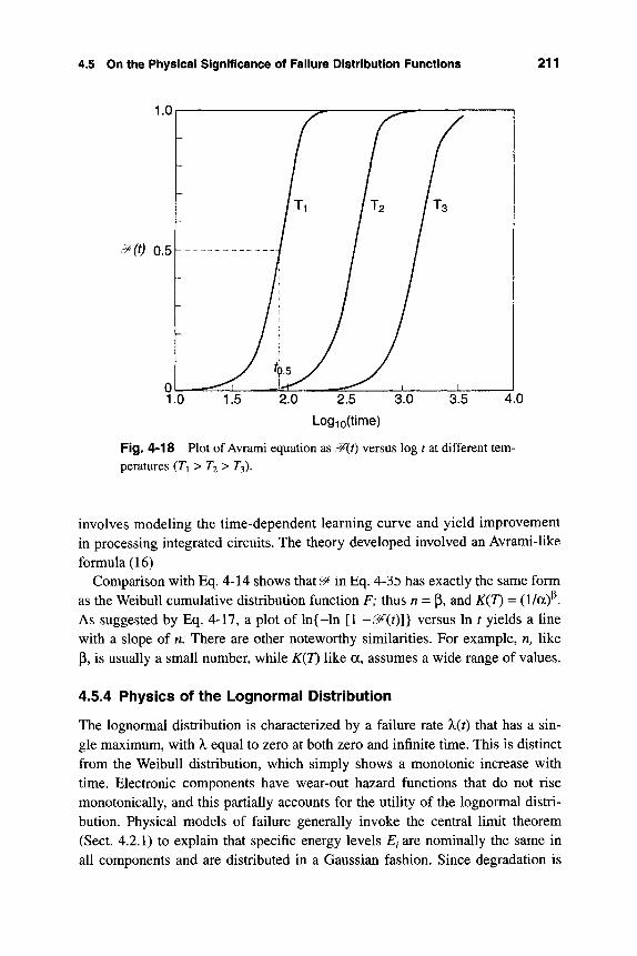
4.5 On the Physical Significance of Failure Distribution Functions 211
^(t) 0.5
2.0 2.5 3.0
Logio(time)
Fig. 4-18 Plot of Avrami equation as ^(t) versus log t at different tem-peratures (Ti > T2> T^).
involves modeling the time-dependent learning curve and yield improvement in processing integrated circuits. The theory developed involved an Avrami-like formula (16)
Comparison with Eq. 4-14 shows that^ in Hq. 4-3^ has exactly the same form as the Weibull cumulative distribution function F; thus n = p, and K(T) = (1/a)'^. As suggested by Eq. 4-17, a plot of ln{-ln [1 -^(t)]} versus In t yields a line with a slope of n. There are other noteworthy similarities. For example, n, like (J, is usually a small number, while K(T) like a, assumes a wide range of values.
4.5.4 Physics of the Lognormal Distribution
The lognormal distribution is characterized by a failure rate X(t) that has a sin-gle maximum, with X equal to zero at both zero and infinite time. This is distinct from the Weibull distribution, which simply shows a monotonic increase with time. Electronic components have wear-out hazard functions that do not rise monotonically, and this partially accounts for the utility of the lognormal distri-bution. Physical models of failure generally invoke the central limit theorem (Sect. 4.2.1) to explain that specific energy levels Ei are nominally the same in all components and are distributed in a Gaussian fashion. Since degradation is
212 The Mathematics of Failure and Reiiabiiity
directly related to the occupancy of such levels according to the Maxwell-Boltz-mann factor, exp [-Ei/kT], the logarithm yields Ei/kT, which is normally distrib-uted; hence the lognormal distribution. Service environments of electronic prod-ucts are relatively benign and vary little among populations. Since the spread in product life is primarily a function of manufacturing variability, it is possible to predict lifetimes on the basis of reliability testing.
In a specific application, Jordan (10) has discussed the aging degradation of GaP red light-emitting diodes in terms of diffusion and accumulation of point defects in the p-n junction region. Explicit expressions for the reduction of the electroluminescent efficiency were derived and had the form of the lognormal function.
There is an interesting inequivalence between the lognormal description of electronic components and the increasing hazard function for human lifetimes (6, 9). For living species, internal aging processes apparently generate species-specific biological clocks with increasing hazard functions as r—>oo. Furthermore, the presence of redundancy at many levels complicates the form of the hazard function. For example, loss of a kidney does not cause death in humans. In addi-tion, random external variables, e.g., bacteria, viruses, accidents, addiction to cig-arettes, alcohol, or drugs, become increasingly life-threatening as the recuperative powers of the body wear out. In contrast to electronic devices, the longevity of humans cannot be predicted with any accuracy through a physical examination.
4.5.5 Acceleration Factor
In recent years electronic devices and components have become very reliable, so that failure rates are now quite low when tested under ambient conditions. How-ever, in order to make more meaningful lifetime projections, many failures, or data points, are required. This can be achieved experimentally through acceler-ated testing. Since many aging mechanisms are governed by the Maxwell-Boltz-mann factor, raising the temperature of the product under test is usually the most effective way to hasten failure.
The acceleration factor (AF), an important term in the subject of reliability, was previously defined as the ratio of the degradation or failure time at the use temperature Ti relative to that at an elevated, accelerated-test temperature T2. In using AF concepts it is assumed that the mechanism of damage does not change in the process. This caveat is an important one. After all, when a hen incubates eggs at room temperature, chicks will hatch; but if the process is accelerated in boiling water, hard boiled eggs result! True acceleration simply means speeding up the action without distorting it in any way. Essentially reproducing Eq. 1-10, the acceleration factor is given by
4.5 On the Physical Significance of Failure Distribution Functions 213
R a t e ( r , ) ^ M T T F ( r O ^ Rate (Ji) MTTF (72) ^
K(J-_1- (4-36)
where the simple symbol E replaces the previously used AG* in all subsequent Arrhenius-type formulas. The activation energy (E) is normally positive, so that when T2 > Ti, AF > 0. More complex expressions for AF arise when driving forces differ at Ti and T2, as noted in Eq. 1-11. For example,
AF = exp | ( J ^ - ^ | . C ( V , - V , ) (4-37)
with C a constant, is commonly used to describe accelerated testing and bum-in under the combined influence of temperature and applied voltage V.
More generally, the question arises as to how to incorporate AF values obtained from accelerated testing under some set of stress-test conditions (s), into reliability functions that are valid under use conditions (u). In the sense used, stresses include temperature, voltage, current, and humidity, taken singly or in combination. True, or linear, acceleration factors apply when every test failure time and distribution function is multiplied by the same constant value to obtain projected results during use. Therefore, tf (u) = AF x tf (s), and the PDF transforms as
U{t) = {\IA¥)xfAtlhV). (4-38)
Similarly, formulas for the cumulative distribution and hazard functions trans-form as
F^{t) = (1/AF) X {AF X Fs (r/AF)} = FltlAF) (4-39)
and
Kit) = (l/AF) X X, (f/AF), (4-40)
respectively. Substitution shows that there is no simple relation between the haz-ard function at use relative to test conditions for the lognormal case, but explicit formulas for the other two distributions are
Exponential K = (1/AF) x X„ (4-41)
Weibull Kit) = (1/AF)P x X,(t) (4-42)
Example 4-5 Tantalum capacitors were tested at elevated temperature, and the failure times were Weibull distributed with scale parameter a = 2.5 x 10^ h and a shape parameter (3 = 0.5. If the acceleration factor is estimated to be 1 x 10" , what is the probability that the capacitors will last 1 year?
214 The Mathematics of Failure and Reliability
Answer The failure probability is given by F(t) = 1 - exp [-(-^^)'^]. In 1 year there are 8760 hours. Therefore, F(8760) = 1 - exp{-[-nn5^^fj^]'''} = 0.00187. Thus the survival probability is equal to 1 - F(8760) or 0.998.
4.5.6 The Arrhenius Model
Rooted in the very nature of atoms and molecules is their thermally activated response to increasing temperature expressed by the Maxwell-Boltzmann or Arrhenius factor (Eq. 1-2). Because of the intimate hnkage of reaction rates, fail-ure times, and acceleration factors, it is natural to incorporate the Arrhenius fac-tor into the probability functions and their derived parameters. However, this involves more than a simple substitution of exp [f (jr - jr)] for AF; whereas AF applies to only two temperatures, the Arrhenius factor is more generally applic-able to a range of temperatures.
The activation energy for degradation and damage processes at the atomic level critically affects the macroscopic mean time to failure through the for-mula
MTTF = A exp E
RT (4-43)
where A is a constant. A list of activation energies for common failure mecha-nisms in silicon devices is included in Table 4-4.
To illustrate how temperature influences failure times, consider the data of Fig. 4-19a, which are plotted in lognormal fashion. In obtaining the activation energy that characterizes these data, lifetimes are picked off the abscissa axis at the ordinate value corresponding to 50% cumulative failures. These times (/50) are defined as MTTF and are plotted in the Arrhenius manner, i.e., log MTTF versus l/T(K), as shown in Fig. 4-19b. From the equation of the resulting straight line,
log MTTF = log A + E/(2303RT) (4-44)
the slope represents £7(2.303 R). Calculation yields a value of E= 1.03 eV. Note that in this case the same activation energy would be obtained when selecting times corresponding to other percentage cumulative failures (e.g., 10%), because the lines are parallel. When this is true it means that the same failure mechanism is probably operative at different temperatures and times.
The same procedure can be followed for Weibull data consisting of a set of parallel failure-distribution lines as a function of time, when plotted at different temperatures. As noted earlier in Eq. 4-17, the slopes yield the value for p; by then reading off times to reach a given F (usually F = ) and plotting them ver-sus 1/r in the Arrhenius manner, the activation energy can be extracted.
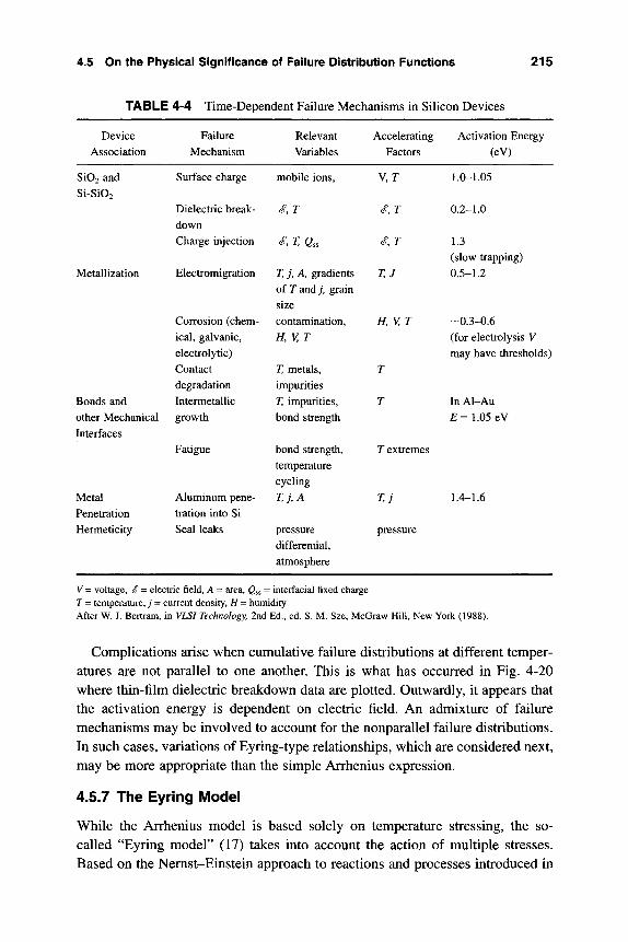
4.5 On the Physical Significance of Failure Distribution Functions 215
TABLE 4-4 Time-Dependent Failure Mechanisms in Silicon Devices
Device Association
Si02 and Si-Si02
Metallization
Bonds and other Mechanical Interfaces
Metal Penetration Hermeticity
Failure Mechanism
Surface charge
Dielectric break-down Charge injection
Electromigration
Corrosion (chem-ical, galvanic, electrolytic) Contact degradation Intermetallic growth
Fatigue
Aluminum pene-tration into Si Seal leaks
Relevant Variables
mobile ions.
S,T
^,T,Q,,
T, j , A, gradients of T and j , grain size contamination. H,V,T
T, metals. impurities T, impurities, bond strength
bond strength, temperature cycling
T.j.A
pressure differential, atmosphere
Accelerating Factors
V, r
(T, r
^, T
T,J
H,VT
T
T
T extremes
T.j
pressure
Activation Energy (eV)
1.0-1.05
0.2-1.0
1.3 (slow trapping) 0.5-1.2
-0.3-0.6 (for electrolysis V may have thresholds)
InAl-Au E= 1.05 eV
1.4-1.6
V = voltage, S' = electric field, A = area, Q^s = interfacial fixed charge T = temperature, j = current density, H = humidity After W. J. Bertram, in VLSI Technology, 2nd Ed., ed. S. M. Sze, McGraw Hill, New York (1988).
Complications arise when cumulative failure distributions at different temper-atures are not parallel to one another. This is what has occurred in Fig. 4-20 where thin-film dielectric breakdown data are plotted. Outwardly, it appears that the activation energy is dependent on electric field. An admixture of failure mechanisms may be involved to account for the nonparallel failure distributions. In such cases, variations of Eyring-type relationships, which are considered next, may be more appropriate than the simple Arrhenius expression.
4.5.7 The Eyring Model
While the Arrhenius model is based solely on temperature stressing, the so-called "Eyring model" (17) takes into account the action of multiple stresses. Based on the Nemst-Einstein approach to reactions and processes introduced in
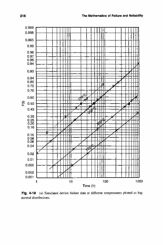
216 The Mathematics of Failure and Reiiabiiity
0.999
0.998
0.995
0.99
0.98 0.97 0.96 0.94
0.90
0.84 0.80 0.75 0.70
0.60
S 0.50
0.40
0.30 0.25 0.20 0.16
0.10 0.08 0.06 0.04
0.02
0.01
0.005
0.002 0.001
1 )
y
/ f \
y \A \/\\
\ \A A\ ^ykW r l
U \A\
\A
9-'
/^ ^
K M >
"TI :br
/ i ( ^ \W M
1 V [A cfn-^
^J( 1 U /\ \jir yicH'
A-ffl r \^\ \
\ \ (
I P Y\ \A \A YP^A' V[\ \A\\
LPK NJ
41II / "
» 1 ^ 1 1
•y Li ^ ifffr m—
iTTT ^ ^
h Itf M
bl LKl
n
M MH
1 1 iH^I 111 hfT T M r i
M KT J M r1
y 1 k
10 100 1000 Time (h)
Fig. 4-19 (a) Simulated device failure data at different temperatures plotted as log-normal distributions.
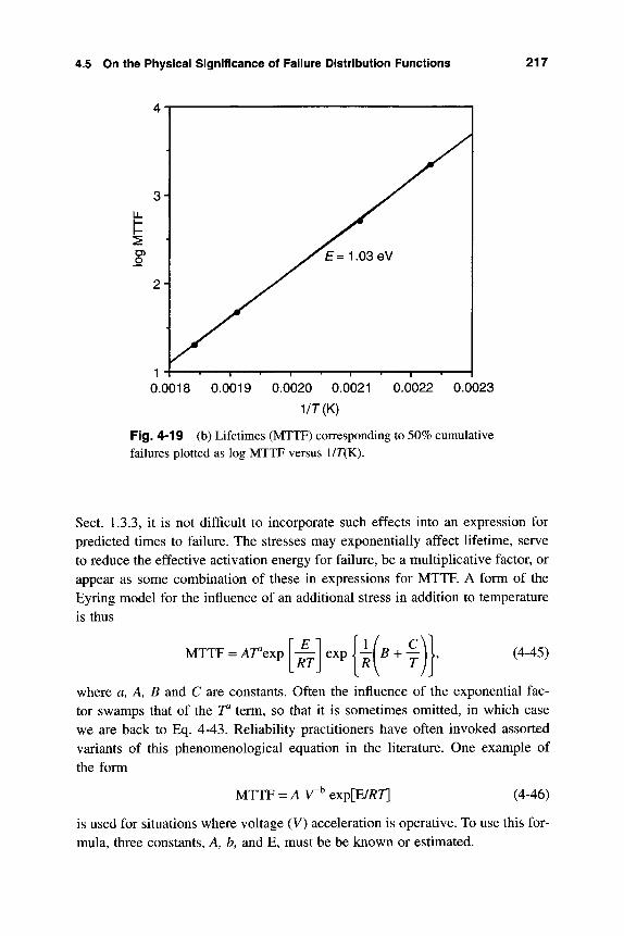
4.5 On the Physical Significance of Failure Distribution Functions 217
4-
0.0018 0.0019 0.0020 0.0021 0.0022 0.0023
1/r(K)
Fig. 4-19 (b) Lifetimes (MTTF) corresponding to 50% cumulative failures plotted as log MTTF versus l/T{K).
Sect. 1.3.3, it is not difficult to incoq)orate such effects into an expression for predicted times to failure. The stresses may exponentially affect lifetime, serve to reduce the effective activation energy for failure, be a multiplicative factor, or appear as some combination of these in expressions for MTTF. A form of the Eyring model for the influence of an additional stress in addition to temperature is thus
MTTF = Arexp RT
(4-45)
where a, A, B and C are constants. Often the influence of the exponential fac-tor swamps that of the V term, so that it is sometimes omitted, in which case we are back to Eq. 4-43. Reliability practitioners have often invoked assorted variants of this phenomenological equation in the literature. One example of the form
MTTF = A V~^ Qxp[E/RT] (4-46)
is used for situations where voltage (V) acceleration is operative. To use this for-mula, three constants, A, b, and E, must be be known or estimated.
218 The Mathematics of Failure and Reliability
400 275
Temperature (C )
200 125 65
A
7.42 MV/cm
8.42 MV/cm
9.42 MV/cm
10.42 MV/cm
11.42 MV/cm
1000/r
Fig. 4-20 Arrhenius plots of mean dielectric breakdown times ( 50) for 15nm thick Si02 films. Data points are derived from lognormal failure distributions obtained at the indicated electric fields. From J. S. Suehle, P. Chaparala, C. Messick, W. M. Miller, and K. C. Boyko, 32nd Annual Proceedings of the IEEE Reliability Physics Symposium, p. 120 (1994). Note that in Fig. 6-13 the activation energy for breakdown is essentially independent of electric field.
4.5.8 Is Arrhenius Erroneous?
Among the issues involving reliability prediction, the exact role of temperature in accelerating failure is one of the most controversial. Traditionally thought to be the prime variable influencing the failure of microelectronics through ther-mal activation of damage mechanisms, Hakim (18) raises the question, "Is Arrhenius erroneous?" This critic contends that lowering the operating temper-ature of equipment will not necessarily improve system reliability. If true, the size of cooling systems in electronic equipment could be reduced, with with no loss of reliability an added bonus. In general, temperature acceleration factors in MIL-HDBK-217 may work well for individual devices and components. But a large proportion of electronic systems failures today are not caused by parts failures but by other events within the system such as electromagnetic interfer-
4.5 On the Physical Significance of Failure Distribution Functions 219
ence, timing problems, electrostatic discharge, and mishandling (19). This again raises questions as to the utility of MIL-HDBK-217.
Pecht et al. (20) have addressed the role of temperature, with an emphasis on those integrated circuit failure mechanisms operative in the range -55°C to 125°C. They suggest that most mechanisms have not quantitatively distin-guished the roles of steady-state temperature, temperature transients, rate of tem-perature rise or drop, and temperature gradients. This assessment is probably correct simply because the admixture of these effects with those of the simulta-neously operative nonthermal stresses, all within the complex geometry and environment of devices, makes failure modeling practically intractable. A conse-quence of this is the wide variability of activation energies reported in Table 4-4. Questions related to whether failures at elevated temperatures are the same as those at use temperatures, and whether mechanisms and activation energies change, have already been raised; they will be addressed again in Sect. 4.6.3.
Blanks (21) in a similar vein has questioned the validity of the Arrhenius rela-tion when nonconstant failure rates prevail. He suggests that the temperature-dependent rate of equipment failure is less than that predicted by the Arrhenius acceleration factor when the hazard rate decreases with time. This implies that failure lifetimes would be underestimated in the case of common lognormal fail-ure distributions. Conversely, when the hazard rate increases with time, the Arrhenius acceleration factor would overestimate equipment failure rates.
The Arrhenius truth of increased atom movements and reaction rates with ris-ing temperature is not being challenged in these collective criticisms. Our igno-rance lies in how to unambiguously isolate and characterize individual damage mechanisms when an admixture or distribution of activation energies may exist. Nevertheless, blaming steady-state temperatures for failures and blindly invok-ing Arrhenius acceleration factors probably shifts emphasis away from design and manufacturing deficiencies in many cases.
4.5.9 The Bathtub Curve Revisited
In Sect. 1.3.8 the famous bathtub curve, so named for its shape, was introduced as a way to plot failure rates over product life cycles. The early failure, or "infant mortality," regime has, for understandable reasons, been the subject of consider-able scrutiny for many years. During short times the weak or marginally func-tional members of the population fail according to a decreasing failure rate. In a model developed at AT&T (22) based on life testing under simulated field condi-tions, the bathtub curve is plotted as the hazard function, or failure rate (in FITs) versus time, as shown in Fig. 4-2la. Early failures are modeled by a Weibull haz-ard function of the form \{t) = X(0) r ( i " P), where 1-p < 1, and X(0) is

220 The Mathematics of Failure and Reliabiiity
lOOOCK)
Ui F U. **—' 1 V . (0
X
10000
1000
100
10 H
^ Exponential Lognormal I Lognon
1 / 1Year I /
^ I I I \ I r * 10 102 103 104 105 106 107
Operating Time (Hours) (a)
Operating Time (b)
Fig. 4-21 (a) Bathtub curve plotted as the hazard function or rate (in FITs) versus log time. The failure rates are typical but do not correspond to any particular device, (b) Roller coaster X(t), which starts high initially, falls to a local minimum (a valley), and then rises up and over a hump finally to merge with flatter portions. From reference 25.
4.5 On the Physical Significance of Faiiure Distribution Functions 221
basically the initial failure rate. On the log ^ - log ^ plot the resulting declining failure rate line is defined by an —20 FIT data point after a period of 10" h, a time somewhat longer than 1 year.
The temperature dependence of infant failures is important because of thermal bum-in screening. Assorted bipolar, MOS, and electro-optical device families have surprisingly exhibited a common low activation energy ranging from 0.25 to 0.4 eV despite the fact that many different failure mechanisms are involved (23). Following elevated temperature stressing, hazard rates at service tempera-tures can be estimated by calculating the appropriate acceleration factor and sub-stituting it into Eq. 4-40. Failures on the left-hand edge of the bathtub curve reflect workmanship defects that include faulty design, omitted inspections, and mishandling. Particulates and contamination during the processing of IC chips are also leading causes of early failures.
Beyond the infant mortality regime is the long, roughly flat portion known as the intrinsic failure period. Failures occur randomly in this region, and the fail-ure rate is approximately constant. Mathematically, the constant hazard rate of the exponential distribution is admirably suited to model such random failures. Most of the useful life of a component is spent here, so that much reliability test-ing is conducted to determine values of X in this region.
Finally, there is the wearout failure regime. Here components degrade at an accelerated pace, so the failure rate increases in this region. This is the regime where lognormal and Weibull statistics enjoy a dominant role. A manufacturing goal for high-reliability components is to extend the life of components prior to the onset of wearout. Remarkable strides have been made in this direction. It should be noted that while experimental failure data for some devices and com-ponents may reflect the entire shape of the bathtub curve, this is not true of the mathematical distribution functions. These distributions fit only one or, at most, two regions of the curve reasonably well.
What has been said thus far about the bathtub curve is the traditional wisdom. For more than a decade this view has been disputed in criticism to the effect that "the bathtub does not hold water any more" (24) and "the roller coaster curve is in" (25) Very low infant mortality failure rates of devices nowadays is the basis for the former observation, while the latter characterization is due to the some-times-observed short time hump in the hazard rate. Thus X(t), which starts high initially, falls to a local minimum (a valley) and then rises up and over a hump to finally merge with flatter portions of the curve, as suggested in Fig. 4-2lb. As far back as 1968, Peck (26) attributed the humps to what he called "freak" fail-ures and suggested that they could be eliminated by stress screening such as bum-in. Later, Peck (27) discerned a considerable lengthening of the infant mor-tality region for integrated circuits to times approaching 100,000 hours. After
222 The Mathematics of Failure and Reiiability
that, the hazard rate apparently meets the main failure distribution. At this stage it becomes an academic question; devices do not actually fail but become obso-lete due to design changes and introduction of new technology.
4.6 PREDICTION CONFIDENCE AND ASSESSING RISK
4.6.1 Introduction
Thus far we have been been blessed with a generous amount of failure data to enable us to readily perform statistical analyses of the kind discussed in this chap-ter. Indeed, much of the electronics reliability physics literature is devoted to accel-erated testing that generates such data in abundance. In practice, however, there are many important situations where there are very few, if any, failures. Military sys-tems, nuclear reactors, airport traffic control systems, undersea communication links, and surgical electronic equipment spring to mind as examples where cata-strophe may result from a single failure. In such cases, how are statistical predic-tions of failure made, and how confident can we be of reliability estimates? What do we do when zero failures are seen in laboratory failure-testing experiments? Questions involving statistically insignificant numbers of failures, and the risks involved in drawing conclusions from them, are addressed in this section (28).
4.6.2 Confidence Limits
The degree of confidence we have in the estimates of [i, a, a, |i, X, or any other statistical quantity mentioned in this chapter is dependent on the number of sam-ples tested and quantity of data, as well as on the error of the statistic under con-sideration. Since the average value for a specific sample will differ from the true value of the population, the latter should be quoted to lie within a range in which we have confidence. The limits that bound this range of values on the high and low ends are known as confidence limits. To be meaningful, reliability projections should be accompanied by a statement of the confidence level. Statistical infer-ence will not inform us of the fate of a particular specimen, but it could, for exam-ple, state that 97% of the components in a population will have an MTTF of 1500 hours. When the population is very large, then its standard deviation will also serve for the specimen itself. There are standard mathematical techniques for evaluating confidence limits, but a discussion of them would take us too far afield. For this information the reader is referred to the indicated references (9,11,29).
More relevant is what happens when very few failures are available for analy-sis. Does it mean that traditional reliability modeling is precluded? Surprisingly,
4.6 Prediction Confidence and Assessing Risic 223
all is not lost! An approach is available to estimate an upper bound for the prob-ability of failure and even to attach a level of confidence to it. Following Nash (9, 28), let us consider a subpopulation of N devices where n failures are seen in time t = ta. The probability of such an outcome is given by the binomial formula (Eq. 3-23), now written in the form
N^ AT
( ^ «) = , / J ' , (^am - F{Qf-\ (4-47) n\ (N- n)\
In this equation F(ta) is the failure function or probability of failure in the time interval t = 0 to t = t^. In the extreme case where there are no failures, n = 0. Since F(t) = 1 - R(t) by Eq. 4-4,
P(0,O = R^(a (4-48)
where R is the reliability or survival function. Because, P (0, to) + P(n > I, ta) = 1 by definition, it follows that the probability of 1 or more failures is given by
P(n>hQ=l-I^(a (4-49)
The problem now reduces to selecting an appropriate functional form of R(ta). As we shall see, R(ta) will contain an undetermined parameter related to a char-acteristic lifetime. Since no failures were observed, a conservative bound on this characteristic lifetime will require that the chance of this occurrence be small. If, for example, P(n > I, to) = 0.95 or 95%, then a lower limit on the characteristic lifetime is such that the actual observation of zero failures is very unlikely, i.e., only 5%. A confidence level C(0), for the case of no failure, is defined to be
C(0) = P(n> l,ta). (4-50)
This value of C(0) is a known quantity that we impose in the analysis. In what follows, expressions for the failure rate will be developed for two dif-
ferent failure models. In the case that failures are described by a WeibuU func-tion,
R(t) = Qxp [-(t/x)^l (4-51)
the characteristic lifetime, x, is used in place of a (see Eq. 4-14). When no fail-ures occur in testing N components for a time t^, then
C(0) = 1 - exp [- mjTfl (4-52)
Suppose we wish to calculate the hazard rate at a specific time, say 1 hour. Then by Eq. 4-15,
?li = p T"^ (4-53)
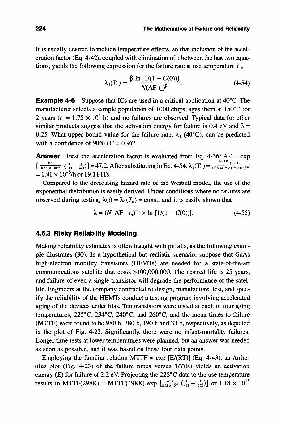
224 The Mathematics of Failure and R^iabillty
It is usually desired to include temperature effects, so that inclusion of the accel-eration factor (Eq. 4-42), coupled with elimination of x between the last two equa-tions, yields the following expression for the failure rate at use temperature T^,
p i n [1 / (1 -go) ) ] .454.
Example 4-6 Suppose that ICs are used in a critical application at 40°C. The manufacturer selects a sample population of 1000 chips, ages them at 150°C for 2 years {t^ = 1.75 x 10" h) and no failures are observed. Typical data for other similar products suggest that the activation energy for failure is 0.4 eV and P = 0.25. What upper bound value for the failure rate, Xi (40°C), can be predicted with a confidence of 90% (C = 0.9)?
Answer First the acceleration factor is evaluated from Eq. 4-36: AF = exp
[ T^TTW^ (3k - ^ ) ] = 47.2. After substituting in Eq. 4-54, Xi(T^) = .^^(..^^Ins'loy^^ = 1.91 xlO-^/hor 19.1 FITS.
Compared to the decreasing hazard rate of the Weibull model, the use of the exponential distribution is easily derived. Under conditions where no failures are observed during testing, X(t) = XxiT^ = const, and it is easily shown that
% = (A - AF • taf^ X In [1/(1 - C(0))]. (4-55)
4.6.3 Risky Reliability Modeling
Making reliability estimates is often fraught with pitfalls, as the following exam-ple illustrates (30). In a hypothetical but realistic scenario, suppose that GaAs high-electron mobility transistors (HEMTs) are needed for a state-of-the-art communications satellite that costs $100,000,000. The desired life is 25 years, and failure of even a single transistor will degrade the performance of the satel-lite. Engineers at the company contracted to design, manufacture, test, and spec-ify the reliability of the HEMTs conduct a testing program involving accelerated aging of the devices under bias. Ten transistors were tested at each of four aging temperatures, 225°C, 234°C, 240°C, and 260°C, and the mean times to failure (MTTF) were found to be 980 h, 380 h, 190 h and 33 h, respectively, as depicted in the plot of Fig. 4-22. Significantly, there were no infant-mortality failures. Longer time tests at lower temperatures were planned, but an answer was needed as soon as possible, and it was based on these four data points.
Employing the familiar relation MTTF « exp [E/(RT)] (Eq. 4-43), an Arrhe-nius plot (Fig. 4-23) of the failure times versus l/r(K) yields an activation energy (£) for failure of 2.2 eV. Projecting the 225°C data to the use temperature results in MTTF(298K) = MTTF(498K) exp [ ^ V ( ^ " 2k)] or 1.18 x 10 ^
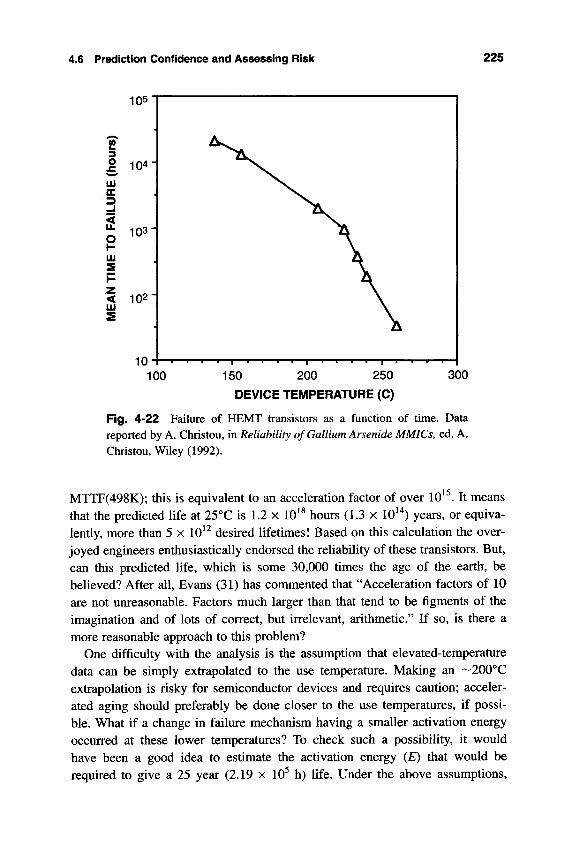
4.6 Prediction Confidence and Assessing Risic 225
250
DEVICE TEMPERATURE (C)
300
Fig. 4-22 Failure of HEMT transistors as a function of time. Data reported by A. Christou, in Reliability of Gallium Arsenide MMICs, ed. A. Ghristou, Wiley (1992).
^15 MTTF(498K); this is equivalent to an acceleration factor of over 10 . It means that the predicted life at 25°C is 1.2 x 10^^ hours (1.3 x 10 " ) years, or equiva^ lently, more than 5 x 10^^ desired lifetimes! Based on this calculation the over-joyed engineers enthusiastically endorsed the reliability of these transistors. But, can this predicted life, which is some 30,000 times the age of the earth, be believed? After all, Evans (31) has commented that "Acceleration factors of 10 are not unreasonable. Factors much larger than that tend to be figments of the imagination and of lots of correct, but irrelevant, arithmetic." If so, is there a more reasonable approach to this problem?
One difficulty with the analysis is the assumption that elevated-temperature data can be simply extrapolated to the use temperature. Making an ~200°C extrapolation is risky for semiconductor devices and requires caution; acceler-ated aging should preferably be done closer to the use temperatures, if possi-ble. What if a change in failure mechanism having a smaller activation energy occurred at these lower temperatures? To check such a possibility, it would have been a good idea to estimate the activation energy (£) that would be required to give a 25 year (2.19 x 10^ h) fife. Under the above assumptions.
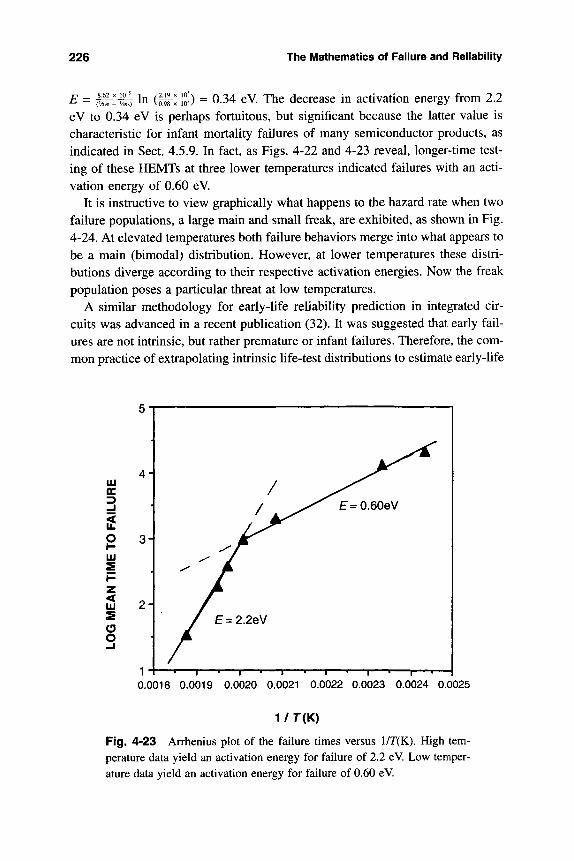
226 The Mathematics of Failure and Reliability
E = ^ - - £ In ( I f H^ ) = 0.34 eV. The decrease in activation energy from 2.2 eV to 0.34 eV is perhaps fortuitous, but significant because the latter value is characteristic for infant mortality failures of many semiconductor products, as indicated in Sect. 4.5.9. In fact, as Figs. 4-22 and 4-23 reveal, longer-time test-ing of these HEMTs at three lower temperatures indicated failures with an acti-vation energy of 0.60 eV.
It is instructive to view graphically what happens to the hazard rate when two failure populations, a large main and small freak, are exhibited, as shown in Fig. 4-24. At elevated temperatures both failure behaviors merge into what appears to be a main (bimodal) distribution. However, at lower temperatures these distri-butions diverge according to their respective activation energies. Now the freak population poses a particular threat at low temperatures.
A similar methodology for early-life reliability prediction in integrated cir-cuits was advanced in a recent publication (32). It was suggested that early fail-ures are not intrinsic, but rather premature or infant failures. Therefore, the com-mon practice of extrapolating intrinsic life-test distributions to estimate early-life
4 1 lU
if
UJ
z 12 2 o o
E=2.2eV
- I 1 1 1 1 1 1 r—^ 1 » 1 »-0.0018 0.0019 0.0020 0.0021 0.0022 0.0023 0.0024 0.0025
1 / T{K)
Fig. 4-23 Arrhenius plot of the failure times versus l/r(K). High tem-perature data yield an activation energy for failure of 2.2 eV. Low temper-ature data yield an activation energy for failure of 0.60 eV.
4.6 Prediction Confidence and Assessing Risk 227
MO
50, 10-2
FREAK POPULATION~\^
JUNCTION TEMPERATURE;
rC) 150^ 100^
MAIN POPULATION
10^ TIME-HRS.
1012
Fig. 4-24 Schematic depiction of failure rate distribution consist-ing of large main and small freak populations. At low temperatures the two populations diverge, with freak failures occurring at short times. After F. R. Nash, Lucent Technologies, Bell Laboratories Innovations.
reliability is incorrect and often leads to unduly optimistic predictions. This all underscores the necessity for screening weak products, some of which may have the potential to cause freak failures.
4.6.4 Freak Failures
The subject of freak failures is perhaps the most difficult topic addressed in reli-ability. Valuable insights into this problem have been provided by Nash (9). Assuring reliability against freak phenomena is open-ended and unstructured because statistically insignificant numbers of freak failures occur. In order to design strategies against freak failures it is instructive to first distinguish between the normal and freak products of manufacture. The reliability of normal products has the following characteristics:
a-1. Failure mechanisms are few in number, e.g., dielectric breakdown, electro-migration, etc.
a-2. These mechanisms are distributed among the entire population of products. a-3. Failures are independent of lot number or time of manufacture. a-4. The normal or statistical variability of manufacturing processes gives rise
to the defects that cause normal failures.
228 The Mathematics of Failure and Reiiabiilty
a-5. Normal failure mechanisms are characterized by well-known activation energies and acceleration factors. Product lifetimes are therefore statisti-cally predictable.
a-6. Importantly, normal products do not fail prematurely. Screening prior to shipment generally weeds out the weak products that would have failed by the normal failure mechanisms.
Abnormal or freak failures, on the other hand, differ from normal failures in all respects. Specifically, they have the following characteristics:
b-1. There are many causes and mechanisms of freak failures. Each one is dif-ferent and occurs with low frequency. Thus freak failures cannot \^ statis-tically modeled. If they could, they would cease to be freak and become normal failures.
b-2. Freak failures are found only in small subsets of the overaD peculation of products.
b-3. Such failures are dependent on lot as well as time of manufacture. b-4. Failure times are often very short and frequently unrelated to operating
times. Freak failures are not wear-out failures! b-5. In contrast to normal failures, there are very few studies of freak failures in
the literature.
Two observations of failures summarize the distinction between normal and abnormal products. Normal products do not fail under anticipated use condi-tions; field failures are of the freak variety.
4.6.5 Minimizing Freak Failures
Is there any hope for a workable strategy to deal with abnormal products? Before answering the question it is helpful to better understand what are thought to be the sources of freak failures. These include:
c-1. Random one-of-a-kind accidents (e.g., electrostatic discharge or electrical overstress due to mishandling).
c-2. Manufacturing processes that are poorly controlled (e.g., particulate conta-mination) or prone to yield low-quality results.
c-3. Changes in the quality or properties of raw materials used (e.g., due to new suppliers).
Based on the last two considerations, the remedies required to minimize the possibility of freak failures are those that continuously improve product qual-ity. Specific measures to improve products for high-reliability applications include:
4.7 A Skeptical and Irreverent Summary 229
d-1. Additional and stricter testing to identify and eliminate products that exhibit signs of being in the least atypical. Tighter pass-fail limits, aging at higher temperatures and bias voltages, and more stages of inspection repre-sent some of the new quality hurdles that should be instituted.
d-2. Laboratory analysis of each and every service failure to establish funda-mental causes of failure. Such information should result in corrective redesign and manufacturing changes aimed at improving the product.
d-3. Implementation of more robust designs with higher safety margins. d-4. Rejection of products that have been reworked. d-5. Institution of traceability to pinpoint faulty processes and identify sus-
pected lots. d-6. Stricter supplier monitoring.
The remainder of this book is primarily concerned with normal failures because virtually the entire reliability physics literature is concerned with them. Unfortunately, this same literature offers little insight into the uncharted territory of freak failures; we therefore travel the more comfortable and well illuminated paths of normal behavior.
4.7 A SKEPTICAL AND IRREVERENT SUMMARY
Now that rather elaborate statistical methods have been presented to analyze degradation and failure data, we may ask how correct and reliable the conclusions are. Skepticism about statistics being able to justify any particular point of view is not solely limited to the social sciences; examples were given in the chapter ques-tioning the validity of the predictions made. I am not the only one to raise such doubts, but rather have humbly followed more eloquent analysts and critics of reliability methodology and its philosophical underpinnings. One such critic is R.A. Evans, an editorial writer for the IEEE Transactions on Reliability, whose column appears in each issue. In these often memorable editorials, many issues related to reliability, statistics, and improving product quality are addressed in a witty and perceptive manner. Several excerpts from this column will give the reader a sense of his concerns and provide a perspective on this chapter.
Statistics and Ignorance
"We spend too much time in our reliability courses on probability and statistical inference . . . that show us how to quantify our ignorance. We do not spend
230 The Mathematics of Failure and Reliability
enough time on removing that ignorance . . . the engineering, physics and chemistry of why things fail and why things don't fail."
from Vol. 39, p. 257, Aug. 1990
Superstition, Witchcraft, Prediction
"The title is a parallel to Disraeli's phrase, "Lies, Damned Lies, and Statistics". . . . A main use of engineering reliability prediction is for the marketplace. That is, a customer wants to know the reliability of a product, before buying the prod-uct. The vagaries of such numbers {predictions for the marketplace) leads to the infamous numbers games."
from Vol. 37, p. 257, Aug. 1988
Statistics vs. Physics
"Statistics describes only populations, not individuals. In particular, the hazard rate (failure rate) of a population does not say anything at all about the behavior of an individual. . . . An individual part is likely to degrade with time, and thus get worse as time goes by; it can do that and still be a member of a constant-haz-ard-rate population. . . . Reliability-statistics is not physics; don't ever confuse them. . . . The quality and reliability disciplines use statistics as a last resort. If we were smarter about the world, we wouldn't have to."
from Vol. 38, p. 273, Aug. 1989
Where Do I Begin?
". . . you are placed in charge of creating a cost-effective reliability program. . . tell me what I should do? . . . Most corrective action will be a combination of management and engineering changes. Some will require scientific advances. A very few will require mathematical advances. Very rarely will mathematical statis-tics be a bottleneck, although some statistical principles are always important. . . . Don't get a bunch of experts to come and lecture everyone on reliability statistics."
from Vol. 38, p. 513, Dec. 1989
Reliability Prediction and MIL-HDBK-217
"One should use MIL-HDBK-217, not because it is so great, but in spite of its weaknesses. When it is used like any other engineering tool, it can be a great help. If it is confused with holy writ, then there is no end of trouble. The search for certainty often ends up in the acceptance of superstition."
from Vol. 37, p. 257, Aug 1988
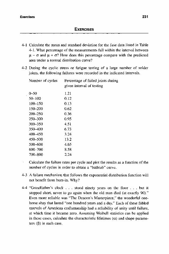
Exercises 231
EXERCISES
4-1 Calculate the mean and standard deviation for the fuse data listed in Table 4-1. What percentage of the measurements fall within the interval between |Li - a and |LI -(- a? How does this percentage compare with the predicted area under a normal distribution curve?
4-2 During the cyclic stress or fatigue testing of a large number of solder joints, the following failures were recorded in the indicated intervals.
Number of cycles Percentage of failed joints during given interval of testing
0-50 50-100 100-150 150-200 200-250 250-300 300-350 350-400 400-450 450-500 500-600 600-700 700-800
1.21 0.12
0.13 0.62
0.36 0.95 4.51 6.73 3.24 13.2
4.65 8.58 2.24
Calculate the failure rates per cycle and plot the results as a function of the number of cycles in order to obtain a "bathtub" curve.
4-3 A failure mechanism that follows the exponential distribution function will not benefit from bum-in. Why?
4-4 "Grandfather's clock . . . stood ninety years on the floor . . . but it stopped short, never to go again when the old man died (at exactly 90)." Even more reliable was "The Deacon's Masterpiece," the wonderful one-horse shay that lasted "one hundred years and a day." Each of these fabled marvels of American craftsmanship had a reliability of unity until failure, at which time it became zero. Assuming Weibull statistics can be applied in these cases, calculate the characteristic lifetimes (a) and shape parame-ters (P) in each case.
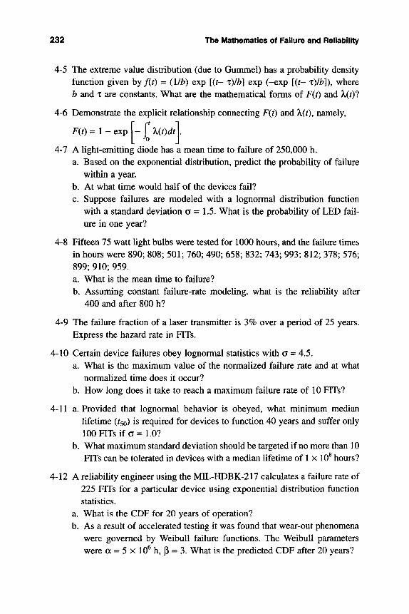
232 The Mathematics of Failure and Reliability
4-5 The extreme value distribution (due to Gummel) has a probabihty density function given by/(0 = (l/b) exp [(t- x)lb\ exp (-exp [{t- x)lb\), where b and T are constants. What are the mathematical forms of F{t) and X{t)l
4-6 Demonstrate the explicit relationship connecting F{t) and X{t), namely,
F{t) = 1 - exp [- I' X{t)dt\,
4-7 A light-emitting diode has a mean time to failure of 250,000 h. a. Based on the exponential distribution, predict the probability of failure
within a year. b. At what time would half of the devices fail? c. Suppose failures are modeled with a lognormal distribution function
with a standard deviation a = 1.5. What is the probability of LED fail-ure in one year?
4-8 Fifteen 75 watt light bulbs were tested for 1000 hours, and the failure times in hours were 890; 808; 501; 760; 490; 658; 832; 743; 993; 812; 378; 576; 899; 910; 959. a. What is the mean time to failure? b. Assuming constant failure-rate modeling, what is the reliability after
400 and after 800 h?
4-9 The failure fraction of a laser transmitter is 3% over a period of 25 years. Express the hazard rate in FITs.
4-10 Certain device failures obey lognormal statistics with a = 4.5. a. What is the maximum value of the normalized failure rate and at what
normalized time does it occur? b. How long does it take to reach a maximum failure rate of 10 FITs?
4-11 a. Provided that lognormal behavior is obeyed, what minimum median lifetime ( 50) is required for devices to function 40 years and suffer only 100 FITs if a = 1.0?
b. What maximum standard deviation should be targeted if no more than 10 FITs can be tolerated in devices with a median lifetime of 1 x 10^ hours?
4-12 A rehability engineer using the MIL-HDBK-217 calculates a failure rate of 225 FITs for a particular device using exponential distribution function statistics.
a. What is the CDF for 20 years of operation? b. As a result of accelerated testing it was found that wear-out phenomena
were governed by Weibull failure functions. The Weibull parameters were a = 5 x 10^ h, p = 3. What is the predicted CDF after 20 years?
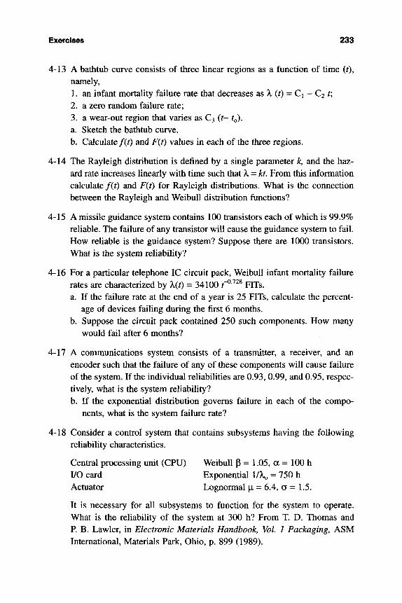
Exercises 233
4-13 A bathtub curve consists of three Hnear regions as a function of time (0, namely, 1. an infant mortality failure rate that decreases as >. (0 = Ci - C2 t; 2. a zero random failure rate; 3. a wear-out region that varies as C3 (t- to). a. Sketch the bathtub curve. b. Calculate/(O and F(t) values in each of the three regions.
4-14 The Rayleigh distribution is defined by a single parameter k, and the haz-ard rate increases linearly with time such that X = kt. From this information calculate f(t) and F(t) for Rayleigh distributions. What is the connection between the Rayleigh and Weibull distribution functions?
4-15 A missile guidance system contains 100 transistors each of which is 99.9% reliable. The failure of any transistor will cause the guidance system to fail. How reliable is the guidance system? Suppose there are 1000 transistors. What is the system reliability?
4-16 For a particular telephone IC circuit pack, Weibull infant mortality failure rates are characterized by X(t) = 34100 T^^^^ FITs. a. If the failure rate at the end of a year is 25 FITs, calculate the percent-
age of devices failing during the first 6 months. b. Suppose the circuit pack contained 250 such components. How many
would fail after 6 months?
4-17 A communications system consists of a transmitter, a receiver, and an encoder such that the failure of any of these components will cause failure of the system. If the individual reliabilities are 0.93, 0.99, and 0.95, respec-tively, what is the system reliability? b. If the exponential distribution governs failure in each of the compo-
nents, what is the system failure rate?
4-18 Consider a control system that contains subsystems having the following reliability characteristics.
Central processing unit (CPU) Weibull [3 = 1.05, a = 100 h I/O card Exponential I/XQ = 750 h Actuator Lognormal |i = 6.4, a = 1.5.
It is necessary for all subsystems to function for the system to operate. What is the reliability of the system at 300 h? From T. D. Thomas and R B. Lawler, in Electronic Materials Handbook, Vol. 1 Packaging, ASM International, Materials Park, Ohio, p. 899 (1989).
234 The Mathematics of Failure and Reiiabiilty
4-19 Sketch what happens to the bathtub curve if a. component dimensions shrink further. b. devices are powered under successively higher current-voltage stressing.
4-20 Consider the bathtub curve for humans. Specify examples of the causes of death that are operative in each of the three time domains.
4-21 A 16-position connector is subjected to 5 different degradation mecha-nisms. The reliabihty for each mechanism is Ri(i = 1-5). a. Write an expression for the overall reliability R of the connector. b. If the Ri are all equal to R^, what is value of Rl c. What contact reliability is required to produce a connector reliability of
0.9999?
4-22 In a population of photodiodes, 20% display freak (f) failures at a mean time to failure of 12,000 h, while the main (m) population has a MTTF of 28000 h. a. Sketch the probability density function, J{t), for this population if they
are normal distributions. b. Suppose a (f) > 2 a (m). What is the ratio of the peak values of/(r), i.e.,
/f(o//m ( ;?
4-23 In GaAs transistors were tested at 180°C, 196°C, and 210°C, and the times to failure in hours were: 180°C: 250, 420,1000, 1300, 1300, 1300,1300, 1500, 1500, 1600 196°C: 190, 200, 330, 330, 400, 400, 420, 600, 800 210°C: 105, 110, 120, 130, 210, 230, 290, 300, 320, 400 a. What are the mean times to failure at each temperature if the data fol-
low lognormal statistics? b. What is the activation energy for failure? c. What is the mean life at 110°C?
4-24 While testing a 10,000 FIT device, 23 failures were observed within the first hour of bum-in. What was the total number of devices in the bum-in lot?
4-25 The overall reaction rate that leads to failure of a component is the result of two mechanisms having different activation energies, Ei and E2. In fail-ure mode A these mechanisms occur in series (sequentially), while for fail-ure mode B they add in parallel. Sketch the overall reaction rate versus temperature in the form of an Arrhenius plot for both failure modes. What are the reliability implications of the thermal dependencies of these two failure modes with respect to predicting low-temperature failure?
References 235
REFERENCES
1. M. G. Pecht and F. R. Nash, Proc. IEEE 82, 992 (1994). 2. P. A. Tobias and D. C. Trindade, Applied Reliability, Van Nostrand Rein-
hold, New York (1986). 3. R E . Fieler, Tutorial Notes, IEEE International Reliability Physics Sympo-
sium, 2.1 (1990). 4. K. L. Wong, Quality and Reliability Engineering International 7,489 (1991). 5. J. A. McLinn, Quality and Reliability Engineering International 6, 237
(1990). 6. W. B. Joyce and R J. Anthony, IEEE Trans, on Reliability 37, 299 (1988). 7. L. R. Goldthwaite, Proc. 7th National Symposium on Reliability and Qual-
ity Control in Electronics, 208 (1961). 8. W. J. Bertram, in VLSI Technology, 2nd. Ed., ed. S. M. Sze, McGraw Hill,
New York (1988). 9. F. R. Nash, Estimating Device Reliability: Assessment of Credibility, Kluwer
Academic, Boston (1993). 10. A. S. Jordan, Microelectronics and Reliability 18, 267 (1978). 11. P. D. T. O'Connor, Practical Reliability Engineering, 2nd Ed., Wiley, Chich-
ester (1986). 12. D. S. Peck, 9th Annual Proceedings of the IEEE Reliability Physics Sympo-
sium, p. 69 (1971). 13. R. Ramakumar, Engineering Reliability—Fundamentals and Applications,
Prentice Hall, Englewood Cliffs, NJ (1993). 14. K. N. Tu, J. W. Mayer, and L. C. Feldman, Electronic Thin Film Science for
Electrical Engineers and Materials Scientists, Macmillan, New York (1992). 15. K. R Rodbell, M. V. Rodriguez, and R J. Ficalora, /. Appl Phys. 61, 2844
(1987). 16. W. Hillberg, Microelectronics and Reliability 20, 337 (1980). 17. H. Eyring, S.H. Lin, and S. M. Lin, Basic Chemical Kinetics, J. Wiley, New
York (1980). 18. E. B. Hakim, Solid State Tech. 33 (8), 57 (1990). 19. R D. T. O'Connor, Solid State Tech. 33 (8), 59 (1990). 20. M. Pecht, P. Lall, and E. B. Hakim, Quality and Reliability Engineering
International 8, 165 (1992). 21. H. S. Blanks, Quality and Reliability Engineering International 6,259 (1990). 22. D. J. Klinger, Y Nakada, and M. A. Menendez, AT&T Reliability Manual,
Van Nostrand Reinhold (1990).
236 The Mathematics of Failure and Reliability
23. D. S. Peck, 16th Annual Proceedings of the IEEE Reliability Physics Sym-posium, p. 1 (1978) and F. S. Beltramo, Proceedings of the Annual Reliabil-ity and Maintainability Symposium, 321 (1988).
24. K. L. Wong, Quality and Reliability Engineering International 4,279 (1988). 25. K. L. Wong, Quality and Reliability Engineering International 5,29 (1989). 26. D. S. Peck, 6th Annual Proceedings of the IEEE Reliability Physics Sympo-
sium, (1968). 27. D. S. Peck, Trans, Electronic Devices 26, 38 (1979). 28. F. R. Nash, Materials Research Society Symposium Proceedings, Vol. 184, 3
(1990). 29. G. W. A. Dummer and N. B. Griffin, Electronics Reliability—Calculation
and Design, Pergamon Press, Oxford (1966). 30. F. R. Nash, Seminar at Stevens Institute, Sept. 27, 1995. 31. R. A. Evans, IEEE Trans, on Reliability 40, 497 (1991). 32. S. S. Menon and K. F. Poole, Microelectronics and Reliability 35, 1147
(1995),
Chapter 5
Mass Transport-Induced Failure
5.1 INTRODUCTION
The preceding chapters have introduced the devices, processing defects, and yields of electronic products that will now see service. Chapter 4 prepared us to expect product failures and provided mathematical tools that enable future per-formance to be predicted. From now until the end of Chapter 10 we shall be pri-marily concerned with the detailed microscopic mechanisms that cause these products to degrade in use. We have already noted (Sect. 1.3.1) that virtually all failures in electronic materials and devices are the result of the physical move-ment of atoms or charge carriers from benign locations associated with normal behavior to other sites where they contribute to creating or enlarging defects that lead to component malfunction. Because solids are often not in thermodynamic equilibrium, atoms feel compelled to move or react. Thus, silicon and aluminum should theoretically revert to Si02 and AI2O3 in air at room temperature, while dopants at junctions should intermix in response to thermodynamic imperatives. But fortunately, for the most part these and other scenarios for change and reac-tion in chemically unstable materials, interfaces, and structures do not occur. The low operating temperatures involved essentially reduce reaction rates to negligi-ble levels. Nevertheless, there are other material combinations and forces present that do pose threats to reliability because the chemical and physical changes they induce are on a scale comparable to device or component feature dimensions.
237
238 Mass Transport-Induced Failure
In this chapter we primarily deal with phenomena attributable to atomic dif-fusional motion on the chip level. This should be distinguished from other trans-port effects treated elsewhere, i.e., electron (Chap. 6), ionic (Chap. 7), and stress-induced flow of solder (Chap. 9). Effects of atomic diffusion include com-pound formation, precipitation reactions, void formation, alloying, contact and interconnect reactions, and general degradation of the metallization. Related examples involve environmentally induced ion migration during corrosion and the permeation of water through plastic packages.
It is a primary objective of this chapter to predict the time dependence of the visible manifestations of failure based on the mass transport models that describe them. Metals are the major culprit associated with mass transport-induced relia-biUty problems at both chip and packaging levels. Degradation and failure phe-nomena due to interdiffusion, compound formation, electromigration, and contact reactions are some of the effects modeled in this chapter.
5.2 DIFFUSION AND ATOM MOVEMENTS IN SOLIDS
5.2.1 Mathematics of Diffusion
Diffusion is defined as the migration of atoms (or molecules) in a matrix under the influence of a concentration-gradient driving force. Through sequential motion of countless numbers of atoms, each jumping from site to site, an observ-able macroscopic change in atomic concentration, C, results. In most cases the diffusing and matrix atoms differ, but they may be the same, as during electro-migration in Al conductors. Pick's law, the phenomenological equation that defines diffusion, is written as
J^ = -DdC/dx. (5-1)
Concentration gradients (dC/dx) in the positive x direction cause transport of a mass flux of atoms (7^) in the negative x direction, signifying that the vectors defining these terms are oppositely directed; hence the negative sign. Flux units mirror those of concentration. For C in atoms/cm^ or g/cm^, the corresponding units of / ^ ^ ^ atoms/cm^-s or g/cm^-s. Irrespective of concentration units, values of Z), the diffu-sion coefficient, or diffusivity, are always expressed in units of (distance)^/time, i.e., cm^/s. The diffusion coefficient, a measure of the extent of mass transport, depends on a number of factors, including the nature of the diffusing atoms and matrix, the specific transport path (i.e., lattice, grain boundary, dislocation, surface, interstitial, etc.), temperature, and the concentration of the diffusing species. Tem-perature, the most important factor influencing Z), was already noted in Eq. 1 -3, while dopant concentration effects in semiconductors were sketched in Sect. 3.2.2.1.

5.2 Diffusion and Atom l\/lovements in Solids 239
During non-steady-state diffusion, more atoms enter a region of the matrix than leave, and therefore, their concentration builds in time (dC/dt > 0). This is normally the case in a homogeneous matrix. But there are situations where more atoms leave a region than enter it. In time this loss of matter (dC/dt < 0) leads to mass depletion or even voids that can adversely affect reliability. Such effects may occur at inter-faces between different phases, or when the matrix is heterogeneous and contains numerous grain boundaries and structural defects. In either case, non-steady-state diffusion can be accounted for by equating the negative divergence of the mass flux (i.e., - V • 7in) to dCldt. When proper account is taken of instantaneous mass con-servation at each value of x, the equation governing diffusion in one dimension is
dt -^ dx' ^^'^^
if D is constant. There is a simple solution to this equation when diffusion occurs in a semi-
infinite matrix, and atoms are supplied at the jc = 0 boundary from an inex-haustible or continuous surface source of concentration C^. Further, it is assumed that the initial concentration in the matrix is Q , or constant throughout, and remains CQ at infinite distance. These initial and boundary conditions may be written as C(x, t = 0) = Q , C(x = 0,t) = C^ (C^ = constant), and C(x = oo^t) = Q . Employing standard boundary-value methods for solving partial differential equations, the solution to Eq. 5-2 is
[C(x,0 - Co]/[Q - Co] = Erfc [x/{4Dt)'% (5-3)
Known as the complementary error function, Erfc [x/(4D0^^^] is mathematically defined as
Erfc [x/{4Dtf^] = 1 - -T72 exp - z dz. (5-4)
An even simpler solution to Eq. 5-2 results if 2i finite or instantaneous rather than continuous surface concentration S (in units of atoms/cm^) is involved. The Gaussian solution has the form
For example, if dopant atoms diffuse into a Si wafer, the amount left on the surface decreases with time; i.e., at jc = 0, C(0,0 = SI{TiDt)^'^. Graphic solutions for contin-uous and finite-source concentration profiles are shown in Fig. 5-1. Like trigono-metric functions, values for the complementary error function and Gaussian are tabulated as a function of the argument [xl{ADtY'^^ in mathematical references and
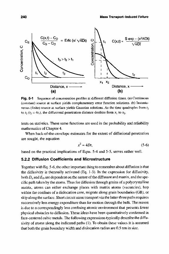
240 Mass Transport-induced Failure
S exp - (x2/4Dt}
X1 X2
Distance, x -(a)
Distance, x -(b)
Fig. 5-1 Sequence of concentration profiles at different diffusion times, (a) Continuous (constant) source at surface yields complementary error function solutions, (b) Instanta-neous (finite) source at surface yields Gaussian solutions. As the time quadruples from ti to t2 (t2 = 4ri), the diffusional penetration distance doubles from xi to X2.
texts on statistics. These same functions are used in the probability and reliability mathematics of Chapter 4.
When back-of-the-envelope estimates for the extent of diffusional penetration are sought, the equation
x^ = 4Dt, (5-6)
based on the practical implications of Eqns. 5-4 and 5-5, serves rather well.
5.2.2 Diffusion Coefficients and lUlicrostructure
Together with Eq. 5-6, the other important thing to remember about diffusion is that the diffusivity is thermally activated (Eq. 1-3). In the expression for diffusivity, both Do and E^ are dependent on the nature of the diffusant and matrix, and the spe-cific path taken by the atoms. Thus for diffusion through grains of a polycrystalline matrix, atoms can either exchange places with matrix atoms (vacancies), hop within the confines of a dislocation core, migrate along grain boundaries (GB), or skip along the surface. Short circuit atom transport via the latter three paths requires successively less energy expenditure than for motion through the bulk. The reason is due to a correspondingly less confining atomic environment that presents fewer physical obstacles to diffusion. These ideas have been quantitatively confirmed in face-centered cubic metals. The following expressions typically describe the diffu-sivity of atoms along the indicated paths (1). To obtain these values it is assumed that both the grain boundary width and dislocation radius are 0.5 nm in size.
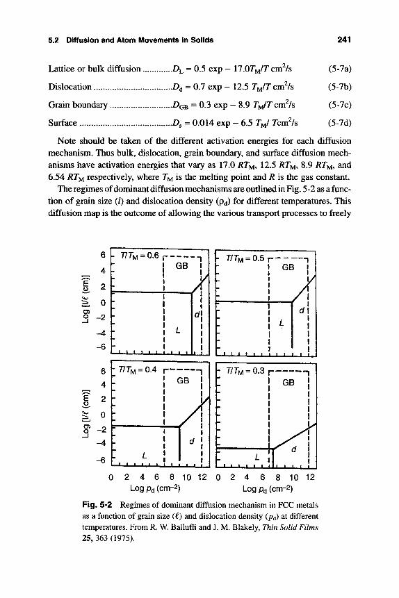
5.2 Diffusion and Atom l\/lovements in Solids 241
Lattice or bulk diffusion D ^ = 0.5 exp - 17.0TM/T cm^/s (5-7a)
Dislocation D^ = 0.7 exp - 12.5 TM/TCW?/S (5-7b)
Grain boundary DGB = 0.3 exp - 8.9 TM/TCWL^S (5-7C)
Surface ...D^ = 0.014 exp - 6.5 T^/ Tcm^/s (5-7d)
Note should be taken of the different activation energies for each diffusion mechanism. Thus bulk, dislocation, grain boundary, and surface diffusion mech-anisms have activation energies that vary as 17.0 RT^, 12.5 RT^, 8.9 RT^, and 6.54 RT^ respectively, where I'M is the melting point and R is the gas constant.
The regimes of dominant diffusion mechanisms are outlined in Fig. 5-2 as a func-tion of grain size (0 and dislocation density (pd) for different temperatures. This diffusion map is the outcome of allowing the various transport processes to freely
E o
O)
o
E o
o
6
4
2
0
-2
-4
-6
. 777] = 0.6 p — - . ^ 1 { GB 1
• \ M
- 1 L.
' 1 1 1 1 1 1 1 1 1
t
1 i
' 1
1..I. J
2 4 6 8 10 12 Logpd(cm-2)
T/TM = 0.5 r n i GB I I I I y
•i i i
t r/TM = o.3r^ n j GB I I I I I I I
•J, i t I
0 2 4 6 8 10 Log Pd (cm-2)
12
Fig. 5-2 Regimes of dominant diffusion mechanism in FCC metals as a function of grain size (€) and dislocation density (p^) at different temperatures. From R. W. Balluffi and J. M. Blakely, Thin Solid Films 25,363(1975).
242 Mass Transport-Induced Failure
compete, where the Hnes represent the conditions for equal mass fluxes from neigh-boring regime mechanisms. Although strictly intended for self-diffusion, we shall assume that the map applies to impurity diffusion as well. In the thin-film regime (shown dotted) at low temperatures, grain boundary diffusion dominates, and therefore GB diffusion coefficients must be used for the purposes of calculation. Even if driving forces other than concentration gradients are operative, micro-scopic atomic migration occurs along these same paths.
Effective diffusivity values vary as a function of grain size, necessitating some sort of averaging of the individual contributions from lattice and GB mecha-nisms. An effective diffusivity, Dg^ = Z)L + / / ) G B has been suggested, where/is the fraction of atoms in short-circuit paths. A measure of/is the ratio of the grain boundary thickness to grain diameter. In general, grain size variations will cor-respondingly cause differing diffusivities.
5.3 BINARY DIFFUSION AND COMPOUND FORMATION
5.3.1 Interdiffusion and the Phase Diagram
Many reliability problems stem from interdiffusion effects at the interface between two dissimilar materials e.g., solder joint, semiconductor contact. To better understand the nature of reaction let us consider a couple consisting of two elements A and B, in contact at a planar interface. What will happen if the cou-ple is now heated to temperature To, where diffusion of atoms normally occurs? The answer depends on the nature of A and B, their grain structures, and the magnitude of the involved diffusivities. A good first step is to look at the phase diagram for A and B. Among the possible reactions are those shown in Fig. 5-3, where solid solution (Fig. 5-3a) and eutectic (Fig. 5-3b) behaviors are depicted. Below each of these, typical interdiffusion profiles are depicted (Fig. 5-3c, d) at Jo and time t. These representations emphasize the connection between phase-concentration distributions and phase diagram-imposed solubility limits. For complete solid-solution systems (e.g., Ge-Si), phases can theoretically assume any binary composition. But in eutectic systems (e.g., Pb-Sn), interdiffusion occurs only up to the solubility limit, resulting in the formation of a range of ter-minal solid solutions.
Concentration profiles in real systems are generally not error-function-like or symmetric across the couple interface, because the diffusivity usually depends on composition and hence position. The rather involved graphic Boltzmann-Matano analysis can yield values for the overall diffusivity, D(Q,
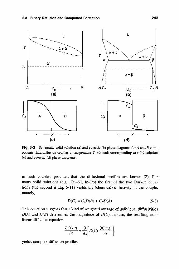
5.3 Binary Diffusion and Compound Formation 243
CA A ^ V ^
- X -
(c)
AQ,
1
C^
^a
a
^
p
(d)
Fig. 5-3 Schematic solid solution (a) and eutectic (b) phase diagrams for A and B com-ponents. Interdiffusion profiles at temperature T^ (dotted) corresponding to solid solution (c) and eutectic (d) phase diagrams.
in such couples, provided that the diffusional profiles are known (2). For many solid solutions (e.g., Cu-Ni, In-Pb) the first of the two Darken equa-tions (the second is Eq. 5-11) yields the (chemical) diffusivity in the couple, namely,
D{C) = CAD(B) + CBD{A) (5-8)
This equation suggests that a kind of weighted average of individual diffusivities D{A) and D{B) determines the magnitude of D{C). In turn, the resulting non-linear diffusion equation.
9C(jc,0 dt
d_ dx
D(Q dC(x,t)
dx
yields complex diffusion profiles.
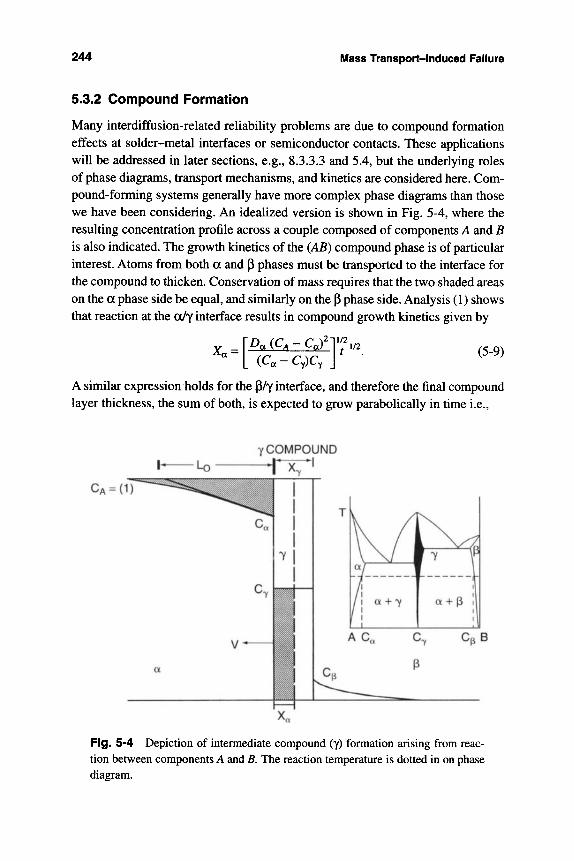
244 Mass lYanspoit-lnduced Failure
5.3.2 Compound Formation
Many interdiffusion-related reliability problems are due to compound formation effects at solder-metal interfaces or semiconductor contacts. These applications will be addressed in later sections, e.g., 8.3.3.3 and 5.4, but the underlying roles of phase diagrams, transport mechanisms, and kinetics are considered here. Com-pound-forming systems generally have more complex phase diagrams than those we have been considering. An idealized version is shown in Fig. 5-4, where the resulting concentration profile across a couple composed of components A and B is also indicated. The growth kinetics of the {AB) compound phase is of particular interest. Atoms from both a and P phases must be transported to the interface for the compound to thicken. Conservation of mass requires that the two shaded areas on the a phase side be equal, and similarly on the P phase side. Analysis (1) shows that reaction at the oc/y interface results in compound growth kinetics given by
" [ {C^-C,)C, J 211/2.
t 1/2 (5-9)
A similar expression holds for the p/y interface, and therefore the final compound layer thickness, the sum of both, is expected to grow parabolically in time i.e..
CA = ( 1 )
YCOMPOUND
CaB
Fig. 5-4 Depiction of intermediate compound (y) formation arising from reac-tion between components A and B. The reaction temperature is dotted in on phase diagram.
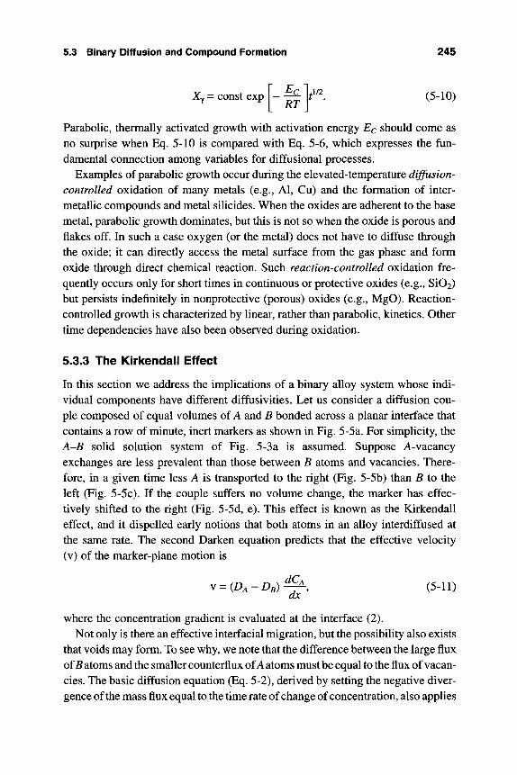
5.3 Binary Diffusion and Compound Formation 245
Xy = const exp RT
f'\ (5-10)
Parabolic, thermally activated growth with activation energy Ec should come as no surprise when Eq. 5-10 is compared with Eq. 5-6, which expresses the fun-damental connection among variables for diffusional processes.
Examples of parabolic growth occur during the elevated-temperature diffusion-controlled oxidation of many metals (e.g., Al, Cu) and the formation of inter-metallic compounds and metal silicides. When the oxides are adherent to the base metal, parabolic growth dominates, but this is not so when the oxide is porous and flakes off. In such a case oxygen (or the metal) does not have to diffuse through the oxide; it can directly access the metal surface from the gas phase and form oxide through direct chemical reaction. Such reaction-controlled oxidation fre-quently occurs only for short times in continuous or protective oxides (e.g., Si02) but persists indefinitely in nonprotective (porous) oxides (e.g., MgO). Reaction-controlled growth is characterized by linear, rather than parabolic, kinetics. Other time dependencies have also been observed during oxidation.
5.3.3 The Kirkendall Effect
In this section we address the implications of a binary alloy system whose indi-vidual components have different diffusivities. Let us consider a diffusion cou-ple composed of equal volumes of A and 5 bonded across a planar interface that contains a row of minute, inert markers as shown in Fig. 5-5a. For simplicity, the A-B solid solution system of Fig. 5-3a is assumed. Suppose A-vacancy exchanges are less prevalent than those between B atoms and vacancies. There-fore, in a given time less A is transported to the right (Fig. 5-5b) than B to the left (Fig. 5-5c). If the couple suffers no volume change, the marker has effec-tively shifted to the right (Fig. 5-5d, e). This effect is known as the Kirkendall effect, and it dispelled early notions that both atoms in an alloy interdiffused at the same rate. The second Darken equation predicts that the effective velocity (v) of the marker-plane motion is
v = ( D ^ - D ^ > ^ , (5-11) dx
where the concentration gradient is evaluated at the interface (2). Not only is there an effective interfacial migration, but the possibility also exists
that voids may form. To see why, we note that the difference between the large flux of atoms and the smaller counterflux of A atoms must be equal to the flux of vacan-cies. The basic diffusion equation (Eq. 5-2), derived by setting the negative diver-gence of the mass flux equal to the time rate of change of concentration, also applies
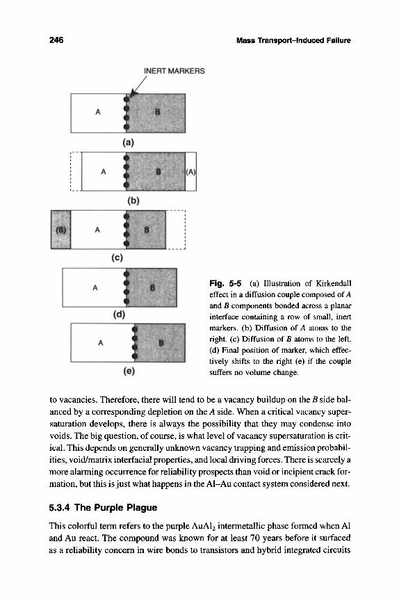
246 Mass Transport-Induced Failure
INERT MARKERS
Fig. 5-5 (a) Illustration of Kirkendall effect in a diffusion couple composed of A and B components bonded across a planar interface containing a row of small, inert markers, (b) Diffusion of A atoms to the right, (c) Diffusion of B atoms to the left, (d) Final position of marker, which effec-tively shifts to the right (e) if the couple suffers no volume change.
to vacancies. Therefore, there will tend to be a vacancy buildup on the B side bal-anced by a corresponding depletion on the A side. When a critical vacancy super-saturation develops, there is always the possibility that they may condense into voids. The big question, of course, is what level of vacancy supersaturation is crit-ical. This depends on generally unknown vacancy trapping and emission probabil-ities, void/matrix interfacial properties, and local driving forces. There is scarcely a more alarming occurrence for reliability prospects than void or incipient crack for-mation, but this is just what happens in the Al-Au contact system considered next.
5.3.4 The Purple Plague
This colorful term refers to the purple AUAI2 intermetallic phase formed when Al and Au react. The compound was known for at least 70 years before it surfaced as a reliability concern in wire bonds to transistors and hybrid integrated circuits
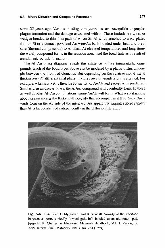
5.3 Binary Diffusion and Compound Formation 247
some 35 years ago. Various bonding configurations are susceptible to purple-plague formation and the damage associated with it. These include Au wires or wedges bonded to thin film pads of Al on Si, Al wires attached to a Au plated film on Si or a contact post, and Au wire/Au balls bonded under heat and pres-sure (thermal compression) to Al films. At elevated temperatures and long times the AuAl2 compound forms in the reaction zone, and the bond fails as a result of annular microcrack formation.
The Al-Au phase diagram reveals the existence of five intermetallic com-pounds. Each of the bond types above can be modeled by a planar diffusion cou-ple between the involved elements. But depending on the relative initial metal thicknesses (d), different final phase mixtures result if equilibrium is attained. For example, when ^^i > ^AU^ then the formation of AuAl2 and excess Al is predicted. Similarly, in an excess of Au, the AIAU4 compound will eventually form. In these as well as other Al-Au combinations, some AUAI2 will form. What is so alarming about its presence is the Kirkendall porosity that accompanies it (Fig. 5-6). Since voids form on the Au side of the interface, Au apparently migrates more rapidly than Al, a fact confirmed independently in the diffusion literature.
Fig. 5-6 Extensive AUAI2 growth and Kirkendall porosity at the interface between a thermosonically formed gold ball bonded to an aluminum pad. From H. K. Charles, in Electronic Materials Handbook, Vol. 1. Packaging, ASM International, Materials Park, Ohio, 224 (1989)
248 Mass Transport-Induced Failure
While AUAI2 alone has an acceptable electrical conductivity and is mechani-cally strong, Kirkendall voids degrade both of these bond properties. The rate at which AUAI2 thickens is given by JCAUAI2 / =1.23 exp [- 1.2 QV/(kT)] (cm^/s), and follows parabolic kinetics (1).
5.4 REACTIONS AT METAL-SEMICONDUCTOR CONTACTS
5.4.1 Introduction to Contacts
Achieving the requisite ohmic or Schottky electrical behavior of contacts first poses challenges in processing, which are then followed by the reliability con-cerns of property change in service. Metal-semiconductor interdiffusion effects at contacts are primarily responsible for reliability problems manifested as short circuits at junctions, increases in contact resistance, and Schottky barrier height variations. These effects are aggravated in devices that pass large currents and heat appreciably. In silicon devices prior to about 1980 aluminum was the con-tact metal of choice. However, as device dimensions shrank, the Al-Si interdif-fusion damage described in the next section led to the adoption of alternative metal-silicide contacts.
New contact metallurgies for Si are less susceptible to reliability problems than metal contacts to GaAs and compound semiconductor devices. Among the reasons for this are (3):
1. GaAs decomposes into Ga and As2 gas at 580°C. 2. The Schottky barrier height ((^Q) is typically —0.8 eV for most metals. An
implication of this is intrinsically high contact resistance. (In contrast, (J)B for Si is -0 .6 eV.)
3. It is difficult to dope «-GaAs to levels higher than 5 x lO^Vcm . 4. Annealing up to 850°C is required to electrically activate dopants following
ion implantation. Therefore, special precautions must be taken to avoid decomposition or melting.
5. Because two elements comprise compound semiconductors, there are more possibilities for reaction with contact metals.
5.4.2 Al-Si Contacts
The problems considered in this section arise during processing rather than ser-vice. Nevertheless, they are instructive, and when extrapolated to low tempera-tures and long times may have reliability implications. We first consider the sim-
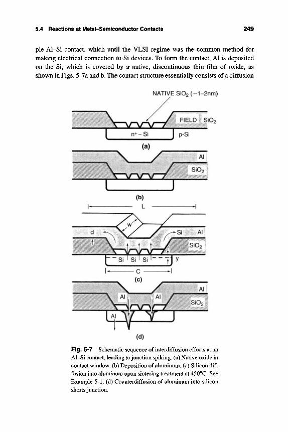
5.4 Reactions at Metal-Semicondactor Contacts 249
pie Al-Si contact, which until the VLSI regime was the common method for making electrical connection to Si devices. To form the contact, Al is deposited on the Si, which is covered by a native, discontinuous thin film of oxide, as shown in Figs. 5-7a and b. The contact structure essentially consists of a diffusion
NATIVE Si02(~1-2nm)
^ JrlELDlSlOa
J P-si
Fig. 5-7 Schematic sequence of interdiffusion effects at an Al-Si contact, leading to junction spiking, (a) Native oxide in contact window, (b) Deposition of aluminum, (c) Silicon dif-fusion into aluminum upon sintering treatment at 450°G. See Example 5-1. (d) Gounterdiffusion of aluminum into silicon shorts junction.
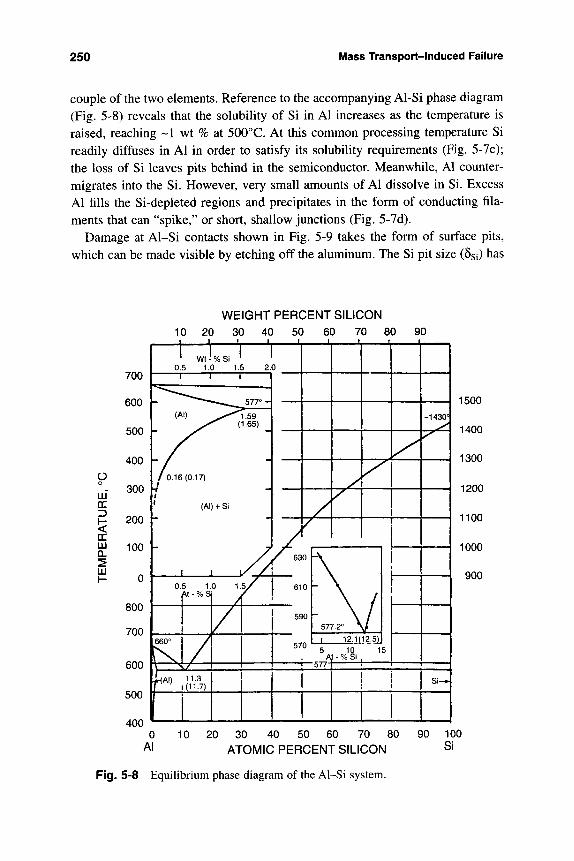
250 Mass Transport-Induced Failure
couple of the two elements. Reference to the accompanying Al-Si phase diagram (Fig. 5-8) reveals that the solubility of Si in Al increases as the temperature is raised, reaching ~1 wt % at 500°C. At this common processing temperature Si readily diffuses in Al in order to satisfy its solubility requirements (Fig. 5-7c); the loss of Si leaves pits behind in the semiconductor. Meanwhile, Al counter-migrates into the Si. However, very small amounts of Al dissolve in Si. Excess Al fills the Si-depleted regions and precipitates in the form of conducting fila-ments that can "spike," or short, shallow junctions (Fig. 5-7d).
Damage at Al-Si contacts shown in Fig. 5-9 takes the form of surface pits, which can be made visible by etching off the aluminum. The Si pit size (5si) has
WEIGHT PERCENT SILICON 10 20 30 40 50 60 70 80 90
O o ui cc Z)
DC LU Q_
700
600
500
400
300
200
100
0
800
700
600
500
400
1 1 J.. '1 '1 ' 1 0.5 1.0 1.5 2.0 1 t i 1
1 .^.^^^577° -
(Al) ^,..^^^^^^59
L .y^""^^ ^^-^^^ ^
/ 0.16 (0.17)
r r (Al) + Si
\ 1 iX /
0.
[660°
5 1. ^t - % S
7 )
li(AI) 11.3 I T 1(11-7)
I
0 1. 7
^ 63
1 •• 5£
/
0
0
)0
570
1
/
1 L
577.2° \ / _ _ 1 12.1(12.5) 5 ^
ii/ r
10 1 f - % S i .
5
! !
-14301
Si-J
1500
1400
1300
1200
1100
1000
900
0 10 20 30 40 50 60 70 80 90 100
Al ATOMIC PERCENT SILICON Si
Fig. 5-8 Equilibrium phase diagram of the Al-Si system.
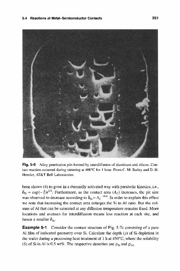
5.4 Reactions at Metal-Semiconductor Contacts 251
Fig. 5-9 Alloy penetration pits formed by interdiffusion of aluminum and silicon. Con-tact reaction occurred during sintering at 400°C for 1 hour. From C. M. Bailey and D. H. Hensler, AT&T Bell Laboratories.
been shown (4) to grow in a thermally activated way with parabolic kinetics; i.e., 6si ~ exp(--|)r^^^. Furthermore, as the contact area (Ac) increases, the pit size was observed to decrease according to 5si ~ Ac ~^'^. In order to explain this effect we note that increasing the contact area enlarges the Si to Al ratio. But the vol-ume of Al that can be saturated at any diffusion temperature remains fixed. More locations and avenues for interdiffusion means less reaction at each site, and hence a smaller 5si.
Example 5-1 Consider the contact structure of Fig. 5-7c consisting of a pure Al film of indicated geometry over Si. Calculate the depth (y) of Si depletion in the wafer during a processing heat treatment of 1 h at 450°C, where the solubility (S) of Si in Al is 0.5 wt%. The respective densities are psi and pAi
252 Mass Transport-Induced Failure
Answer The amount of Si needed to saturate the metal contact structure depends on the Al volume as well as the solubility of Si in Al. Conservation of mass requires that the amount of Si lost beneath the contact window must equal that which enters the metal. For (polycrystalline) Al-(single crystal) Si couples, the diffusivity of Si in Al is given by D = 25 x 10"^ exp [-0.79 tWI(kT)] cmVs (3). By Eq. 5-6, the total diffusion length (L) along both sides of the contact at 450°C is calculated to be L = 4 x {(25 x 10"^ exp [-0.79 eV/8.62 x 10"^ x 723]) x 3600}^^^ = 1.07 X 10"^ cm (107 ^im). Therefore, Lwd^p^xS^wCy psi- Solv-ing, y = ^ ^ . Substituting pAi = 2.7, psi = 2.33, and assuming w = 2 iim;d = 1 liim, and C = 5 |xm, y is calculated to be 0.123 [im.
This example shows that direct Al-Si contact cannot be tolerated under any cir-cumstances, because the reaction dimensions are uncomfortably large compared to device junction depths. The use of Al metallizations saturated with greater than 1 wt% Si eliminates the driving force for these interdiffusion effects. But when this alloy cools. Si precipitates as its solubility declines; leaving nodules behind on the semiconductor surface. These nodular islands are p (Al) doped and gener-ally raise the contact resistance. Similar but generally more severe interdiffusion effects result from reaction between Al and polycrystalline Si (polysilicon) films. Diffusion and reaction lengths are expected to be larger for polysilicon.
5.4.3 Metal Silicide Contacts to Silicon
To protect submicron-deep junctions against the intrusion of the Al metallization, diffusion barriers composed of metal silicides, or Ti-W alloys are commonly interposed to limit interdiffusion between Al and Si. Silicides are metals with resistivities of- 15-50 \iQ-cm, which is considerably higher than the value for Al (2.8 |iQ-cm). They are formed by reacting refractory metal films deposited on Si wafers. Rather than the pitted Al-Si interface, the resulting silicide layers yield very stable planar and uniformly thick contacts. Silicides that have seen use in microelectronics applications are listed in Table 2-1 together with some of their properties. These contacts are relatively immune to degradation in normal service. Problems do, however, arise at elevated temperatures during electromigration, and such effects in TiSi2 and TaSi2 contacts will be discussed in Sect. 5.6.1.1.
Silicides not only provide necessary electrical contact functions, but also serve as diffusion barriers. Occasionally, Al and the silicide chemically combine so that the fundamental problem of curbing Al reactivity remains. As an exam-ple of the potential degradation of metal silicides consider the case of PtSi (5). This intermetallic has been used in microelectronics because it makes nearly ideal ohmic and Schottky barrier contacts. However, the reaction between Al interconnects and PtSi at a Si contact yields the PtAl2 intermetallic compound
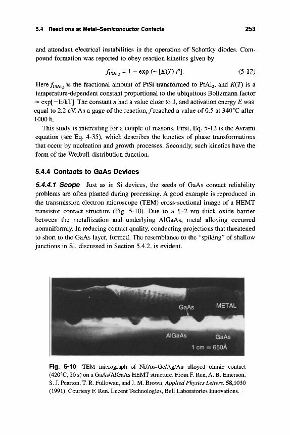
5.4 Reactions at Metal-Semiconductor Contacts 253
and attendant electrical instabilities in the operation of Schottky diodes. Com-pound formation was reported to obey reaction kinetics given by
/ptAi2 = 1 - exp (-[ir(7) f ]. (5-12)
Here /ptAi2 is the fractional amount of PtSi transformed to PtAl2, and K(T) is a temperature-dependent constant proportional to the ubiquitous Boltzmann factor ~ exp[-E/kT]. The constant n had a value close to 3, and activation energy E was equal to 2.2 eV As a gage of the reaction,/reached a value of 0.5 at 340°C after 1000 h.
This study is interesting for a couple of reasons. First, Eq. 5-12 is the Avrami equation (see Eq. 4-35), which describes the kinetics of phase transformations that occur by nucleation and growth processes. Secondly, such kinetics have the form of the Weibull distribution function.
5.4.4 Contacts to GaAs Devices
5.4.4,1 Scope Just as in Si devices, the seeds of GaAs contact reliability problems are often planted during processing. A good example is reproduced in the transmission electron microscope (TEM) cross-sectional image of a HEMT transistor contact structure (Fig. 5-10). Due to a 1-2 nm thick oxide barrier between the metallization and underlying AlGaAs, metal alloying occurred nonuniformly. In reducing contact quality, conducting projections that threatened to short to the GaAs layer, formed. The resemblance to the "spiking" of shallow junctions in Si, discussed in Section 5.4.2, is evident.
Fig. 5-10 TEM micrograph of Ni/Au-Ge/Ag/Au alloyed ohmic contact (420°€, 20 s) on a GaAs/AlGaAs HEMT structure. FromF. Ren, A. B. Emerson, S. J. Pearton, T. R. Fullowan, and J. M. Brown, Applied Physics Letters. 58,1030 (1991). Courtesy F. Ren, Lucent Technologies, Bell Laboratories Innovations.
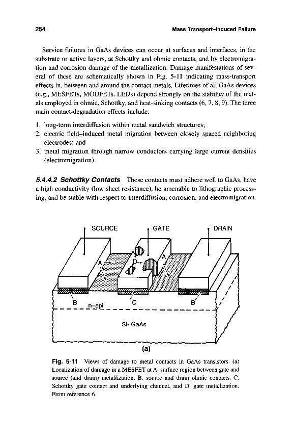
254 Mass Transport-Induced Failure
Service failures in GaAs devices can occur at surfaces and interfaces, in the substrate or active layers, at Schottky and ohmic contacts, and by electromigra-tion and corrosion damage of the metallization. Damage manifestations of sev-eral of these are schematically shown in Fig. 5-11 indicating mass-transport effects in, between and around the contact metals. Lifetimes of all GaAs devices (e.g., MESFETs, MODFETs, LEDs) depend strongly on the stability of the met-als employed in ohmic, Schottky, and heat-sinking contacts (6, 7, 8, 9). The three main contact-degradation effects include:
1. long-term interdiffusion within metal sandwich structures; 2. electric field-induced metal migration between closely spaced neighboring
electrodes; and 3. metal migration through narrow conductors carrying large current densities
(electromigration).
5,4,4.2 Schottky Contacts These contacts must adhere well to GaAs, have a high conductivity (low sheet resistance), be amenable to lithographic process-ing, and be stable with respect to interdiffusion, corrosion, and electromigration.
r SOURCE GATE DRAIN
Fig. 5-11 Views of damage to metal contacts in GaAs transistors, (a) Localization of damage in a MESFET at A. surface region between gate and source (and drain) metallization, B. source and drain ohmic contacts, C. Schottky gate contact and underlying channel, and D. gate metallization. From reference 6.
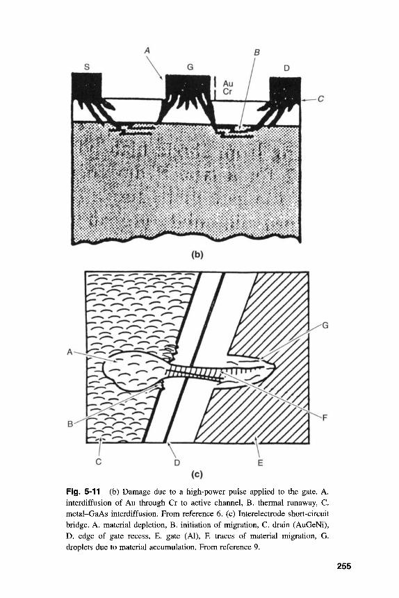
Fig. 5-11 (b) Damage due to a high-power pulse appHed to the gate. A. interdiffusion of Au through Cr to active channel, B. thermal runaway, C. metal-GaAs interdiffusion. From reference 6. (c) Interelectrode short-circuit bridge. A. material depletion, B. initiation of migration, C. drain (AuGeNi), D. edge of gate recess, E. gate (Al), F. traces of material migration, G. droplets due to material accumulation. From reference 9.
255

256 Mass Transport-Induced Failure
Only a few metals possess this complement of properties, with Al and Ti being the most commonly employed. In the case of Al, two specific failure mecha-nisms have been identified, namely Al/GaAs interdiffusion and electromigration. Accompanying the degradation at the Al/GaAs interface is an undesirable increase in electron barrier height, typically from 0.7 to 0.9 eV. While Al/GaAs contacts are thermally stable, the same is not true for Ti, which readily oxidizes. This makes wire bonding difficult, a problem solved by a Au overlayer. How-ever, the Au/Ti/GaAs contact structure is unstable at temperatures as low as 200°C. The solution here as in Si technology is to interpose diffusion barriers that minimize, but do not totally eliminate, reactions between Au and Ti. Metals such as Pt, W, Pt/Cr, and Pd have been used for this purpose.
Diffusion of Au into GaAs after penetrating through metal-barrier layers is a primary failure mechanism in Au-based gate metallizations. When this happens, the metal/semiconductor interface advances into the channel, narrowing its effective thickness. In addition, diffused metal alters the net donor concentration in the channel and modifies device behavior.
Typical activation energies for degradation of Al contacts range from 0.8 to 1.0 eV. Reflecting greater stability, the corresponding activation energies for Au-based contacts are larger, and values of 1.5-1.8 eV have been reported.
5.4,4.3 Ohmic Contacts Parasitic contact resistance at source and drain ohmic contacts influences a number of FET device parameters (transconduc-tance, saturation current, etc.). The most widely used metallization for ohmic contacts to GaAs is derived from a Au-Ge eutectic alloy covered by a Ni layer to improve wettability. The resulting AuGeNi possesses low contact resistance required for high-frequency and high-power applications. Increases in contact resistance have been attributed to four effects:
1. Outdiffusion of Ga and As from GaAs and subsequent reaction with the con-tact metal. A nonstoichiometric defect-rich region is then left behind under the contact.
2. Indiffusion of Ga. 3. The doping density in the semiconductor is reduced by indiffusion of Au and Ni. 4. Formation of NiAsGe, AuGa, and Ni2GeAs compound phases. This reduces
the effective contact area.
Among the interesting manifestations of damage in unpassivated GaAs MES-FETs are AS2O3 polyp growths over ohmic contacts containing Au (10). A model for their growth suggests that As is liberated as a byproduct of GaAs dissocia-tion by Au, a reaction that results in the formation of a AuGa alloy. Room tem-perature Kirkendall-like interdiffusion between Ga and Au facilitates the simul-
5.4 Reactions at Metal-Semiconductor Contacts 257
taneous migration of As to the contact surface, where it oxidizes. Passivation protection against moisture minimizes the occurrence of such damage.
5.4.4.4 Gate Sitlking Diffusion of gate metals into the underlying GaAs effectively reduces the thickness of the active layer, an effect known as "gate sinking." The change in device pinch-off voltage (Vp), a degradation mode suf-fered by GaAs MESFETS, is a consequence of gate sinking (11). A diffusion model to explain this effect is based on the metal migration that occurs. For one-dimensional diffusion of the Schottky contact metal into GaAs we have for con-stant surface concentration, C^ (Eq. 5-3),
C(x,t) = Cs Erfc i4Dtf^
(5-13)
Assuming that the metal front is at depth X^ with a concentration of ~10~^, then Xd == 2.75 X 2 {Dt)^'^. Theory shows that the pinch-off voltage in an active layer of thickness W, reduced in time t by Zd, is given by
qN{W-X^f " " 2 8 "'
Vp(0 = - ^ ' L + Vo, . (5-14)
where A is the effective layer doping level, q is the electronic charge, 8 is the effective dielectric constant, and VQ is the built-in voltage. Relative to the initial pinch-off voltage, Vp (0) = ^=^ + VQ, the change is given by
A[Vp]=-^A^XdW/8, (5-15)
where it is assumed that VQ is constant and Xd/(2W) < 1. Therefore, it is predicted that the pinch-off voltage drifts parabolically with
time according to
A[yp(n 7)] = ^ ^ ^ ^ m r exp - ^ (5-16)
by combining previous equations and decomposing the temperature-dependent diffusivity into constants D^ and E^. Comparison of Eq. 5-16 with the measured behavior of MESFETs is made in Fig. 5-12a and lends support to the proposed diffusion model.
5.4.4,5 Failure in MODFETs Mechanisms for MODFET failure have been sunmiarized by Anderson (7) and include those mentioned earlier. Contact degradation and gate interdiffusion are the most common; Thus gate sinking from Schottky contacts, in addition to effectively thinning the AlGaAs layer, alters Schottky barrier heights. Interdiffusion of ohmic contact metal into GaAs
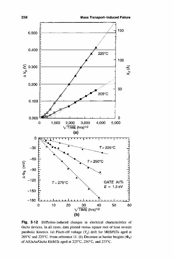
258 Mass Transport-Induced Failure
0.500
0.400
> 0.300 Q.
>
0.200 t
0.100
0.000
• H 150
H 100
X
1,000 2,000 3,000 4,000 5,000 VTIME (hrs)i/2
(a) ffj>j.j t I 1 I I I I > I I I I I I I I I I I I I ; I I I I J
>
CO
e <
-120 h
-150 E-
-180
-30 t '^^ •'
-60 h
-90 h
T= 225°C
- . ^^^t
*-. T= 250°C
i I I
T= 275°C
I I
GATE Al/Ti E = 1.3 eV H
I i I I I T i 1 I 1 1 I I
10 20 30 40 V r i M E (hrs)i/2
(b)
50 60
Fig. 5-12 Diffusion-induced changes in electrical characteristics of GaAs devices. In all cases, data plotted versus square root of time reveals parabolic kinetics, (a) Pinch-off voltage (Vp) drift for MESFETs aged at 205°C and 225°C. From reference 11. (b) Decrease in barrier heights (OB) of AlGaAs/GaAs HEMTs aged at 225°C, 250°C, and 275°C.

5.5 Electromigration Physics and Damage Models 259
35
30 b
25 h
c
Q .
CO
DC 15 h
10
"2 r~
Z. "Z -^ ^
"" -'-I~ I • "
[I" h-1
- , " - > ' ' *- - -«'
1 1 1 1 1 1 1 1 1 1 1 1 \ 1 T"
>«' *'
T= 275°C a,
E = 1.6 eV a
p'
p y'. T= 250°C
A
,''' • ^ ' y
. - A - - ' - - -* A / ' . ' • . . ^ " ,' ,'' A , . - - - - ' :-' ^,...^ " ' r=225°c . - " * ' " ' 1 1 1
1 1 \ 1 1 1 1 1 1 1 1 1 1 1 L_
'~TZ.
Hi
-—
_ "" -- •
" ~ •^ ~z -~ q j
l 1
20 40 V T I M E (hrs)i/2
(c)
60 70
Fig. 5-12 (c) Increase in parasitic source resistance (Rs) of AlGaAs/ GaAs HEMTs aged at 225°C, 250°C and 275°C. From reference 6.
apparently causes electron trapping, establishing a barrier to current flow. Deconfinement of the two-dimensional electron gas (Sect. 2.7.4), together with reduction of carrier mobility and saturation velocity, are other suggested conse-quences of the diffusion of either contact metal, dopants, or semiconductor con-stituents. The parabolic kinetics of change in barrier height and source resistance shown in Figs. 5-12b and c lend further credence to diffusion-based degradation mechanisms. These effects are not solely limited to GaAs-based HEMTs. A recent study on 0.1 |im gate length InP HEMTs (12) revealed a transconductance decrease as a result of gate sinking. The kinetics of degradation were parabolic with time, and defined by an activation energy of 1.26 eV.
5.5 ELECTROMIGRATION PHYSICS AND DAMAGE MODELS
5.5.1 Introduction
Electromigration, a phenomenon not unlike electrolysis, is characterized by the migration of metal atoms in a conductor through which large direct-current densi-ties (/e) pass. It occurs in pure metals as well as in alloys and has been suggested as a mechanism for failure of tungsten filaments in light bulbs. Lamp filament fail-
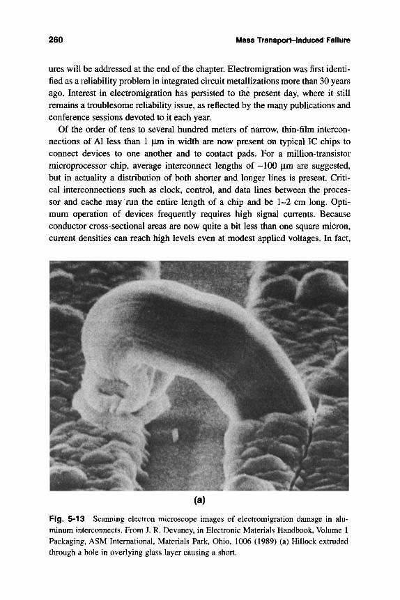
260 Mass Transport-Induced Failure
utes will be addressed at the end of the chapter. Electromigration was first identi-fied as a reliability problem in integrated circuit metallizations more than 30 years ago. Interest in electromigration has persisted to the present day, where it still remains a troublesome reliability issue, as reflected by the many publications and conference sessions devoted to it each year.
Of the order of tens to several hundred meters of narrow, thin-film intercon-nections of Al less than 1 p.m in width are now present on typical IC chips to connect devices to one another and to contact pads. For a million-transistor microprocessor chip, average interconnect lengths of -100 |xm are suggested, but in actuality a distribution of both shorter and longer lines is present. Criti-cal interconnections such as clock, control, and data lines between the proces-sor and cache may run the entire length of a chip and be 1-2 cm long. Opti-mum operation of devices frequently requires high signal currents. Because conductor cross-sectional areas are now quite a bit less than one square micron, current densities can reach high levels even at modest applied voltages. In fact.
Fig. 5-13 Scanning electron microscope images of electromigration damage in alu-minum interconnects. From J. R. Devaney, in Electronic Materials Handbook, Volume 1 Packaging, ASM International, Materials Park, Ohio, 1006 (1989) (a) Hillock extruded through a hole in overlying glass layer causing a short.
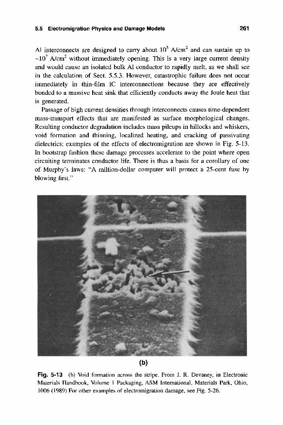
5.5 Electromigration Physics and Damage Models 261
Al interconnects are designed to carry about 10^ A/cm^ and can sustain up to -10^ A/cm^ without immediately opening. This is a very large current density and would cause an isolated bulk Al conductor to rapidly melt, as we shall see in the calculation of Sect. 5.5.3. However, catastrophic failure does not occur inmiediately in thin-film IC interconnections because they are effectively bonded to a massive heat sink that efficiently conducts away the Joule heat that is generated.
Passage of high current densities through interconnects causes time-dependent mass-transport effects that are manifested as surface morphological changes. Resulting conductor degradation includes mass pileups in hillocks and whiskers, void formation and thinning, localized heating, and cracking of passivating dielectrics; examples of the effects of electromigration are shown in Fig. 5-13. In bootstrap fashion these damage processes accelerate to the point where open circuiting terminates conductor life. There is thus a basis for a corollary of one of Murphy's laws: "A million-dollar computer will protect a 25-cent fuse by blowing first."
Fig. 5-13 (b) Void formation across the stripe. From J. R. Devaney, in Electronic Materials Handbook, Volume 1 Packaging, ASM International, Materials Park, Ohio, 1006 (1989) For other examples of electromigration damage, see Fig. 5-26.
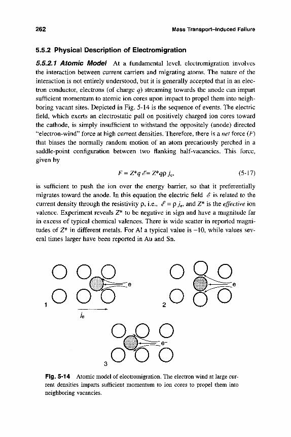
262 Mass Transport-Induced Failure
5.5.2 Physical Description of Electromigration
5,5.2,1 Atomic Model At a fundamental level, electromigration involves the interaction between current carriers and migrating atoms. The nature of the interaction is not entirely understood, but it is generally accepted that in an elec-tron conductor, electrons (of charge q) streaming towards the anode can impart sufficient momentum to atomic ion cores upon impact to propel them into neigh-boring vacant sites. Depicted in Fig. 5-14 is the sequence of events. The electric field, which exerts an electrostatic pull on positively charged ion cores toward the cathode, is simply insufficient to withstand the oppositely (anode) directed "electron-wind" force at high current densities. Therefore, there is a net force (F) that biases the normally random motion of an atom precariously perched in a saddle-point configuration between two flanking half-vacancies. This force, given by
F = Z^qc^=Z*qpU (5-17)
is sufficient to push the ion over the energy barrier, so that it preferentially migrates toward the anode. In this equation the electric field (o is related to the current density through the resistivity p, i.e., S' = p^e. and Z* is the effective ion valence. Experiment reveals Z* to be negative in sign and have a magnitude far in excess of typical chemical valences. There is wide scatter in reported magni-tudes of Z* in different metals. For Al a typical value is -10, while values sev-eral times larger have been reported in Au and Sn.
o o ^
Fig. 5-14 Atomic model of electromigration. The electron wind at large cur-rent densities imparts sufficient momentum to ion cores to propel them into neighboring vacancies.
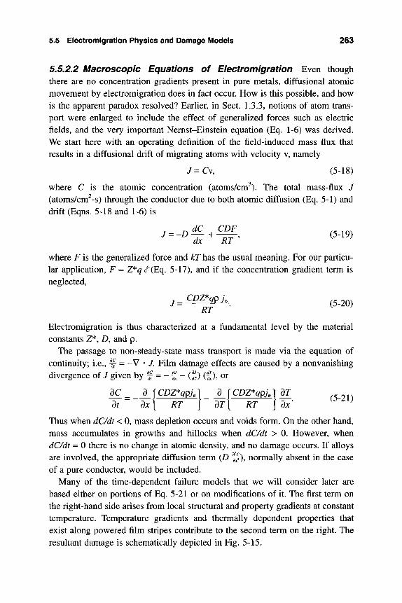
5.5 Electromigration Physics and Damage Models 263
5.5.2.2 Macroscopic Equations of Eiectromigration Even though there are no concentration gradients present in pure metals, diffusional atomic movement by electromigration does in fact occur. How is this possible, and how is the apparent paradox resolved? Earlier, in Sect. 1.3.3, notions of atom trans-port were enlarged to include the effect of generalized forces such as electric fields, and the very important Nemst-Einstein equation (Eq. 1-6) was derived. We start here with an operating definition of the field-induced mass flux that results in a diffusional drift of migrating atoms with velocity v, namely
y=Cv, (5-18)
where C is the atomic concentration (atoms/cm^). The total mass-flux / (atoms/cm^-s) through the conductor due to both atomic diffusion (Eq. 5-1) and drift (Eqns. 5-18 and 1-6) is
J = - D ^ ^ ^ , (5-19) dx RT
where F is the generalized force and kT has the usual meaning. For our particu-lar application, F = Z^q ^(Eq. 5-17), and if the concentration gradient term is neglected,
j^CDI^^^n.^ (5-20) RT
Electromigration is thus characterized at a fundamental level by the material constants Z*, D, and p.
The passage to non-steady-state mass transport is made via the equation of continuity; i.e., ^ = -V • 7. Film damage effects are caused by a nonvanishing divergence of J given by f = - | - (f) (f), or
dt dx CDZ^gQJ,
RT
d {CDZ^qQJ, dT[ RT
f . (5-21) ax
Thus when dC/dt < 0, mass depletion occurs and voids form. On the other hand, mass accumulates in growths and hillocks when dC/dt > 0. However, when dC/dt = 0 there is no change in atomic density, and no damage occurs. If alloys are involved, the appropriate diffusion term (D 0 ) , normally absent in the case of a pure conductor, would be included.
Many of the time-dependent failure models that we will consider later are based either on portions of Eq. 5-21 or on modifications of it. The first term on the right-hand side arises from local structural and property gradients at constant temperature. Temperature gradients and thermally dependent properties that exist along powered film stripes contribute to the second term on the right. The resultant damage is schematically depicted in Fig. 5-15.
264 Mass Transport-Induced Failure
Temperature
Fig. 5-15 Schematic model of damage in an interconnect subject to electromigration. Hillocks and voids develop in response to temperature gradients superimposed on the directed electron current flow.
5.5.3 Temperature Distribution in Powered Conductors
Before addressing material transport during electromigration it is instructive to consider the separate issue of heat transfer in powered metal wires. Calculation of the temperature attained is a useful prelude to estimating the current passed prior to failing. Such an analysis (13, 14) is applicable to the behavior of fuses that cause an open circuit by melting.
Let us first consider current / (A) passing through a wire of length L and cross-sectional area A whose electrical resistivity is p (Q-cm) and thermal conductiv-ity is K (W/cm-K). Assuming no heat loss by radiation or convection, the non-steady-state heat flow equation describing the temperature (7) at any position {x) may be written as
5. ^ ^
dt
9 ^ 4 2 ' (5-22)
with 5 and c the wire density and heat capacity, respectively. (Note that K/5C is the thermal diffusivity, which has units of cm^/s.) In addition to the two familiar terms in Eq. 5-22, the rate of heat generation must be considered. In a short length of resistor wire dx long, this amounts to f" p dxlA. Thermal and electrical conductivities (a, where a = 1/p) of metals are theoretically connected by the well-known Weidemann-Franz law, expressed by a = KILT, where L is the Lorenz number, a constant equal to 2.44 x 10"^ W-Q/K^. In the steady state.
5.5 Electromigration Physics and Damage Models 265
dT/dt = 0, and therefore Eq. 5-22 now assumes the far simpler form of the har-monic oscillator equation,
^ + B^T=0, (5-23) dx
where B^ = i^ Ll(A^ K^). The physical problem we now address is a conductor whose ends are main-
tained at ambient temperature T^. Wirebonds that connect silicon chips to metal lead frames approximate this geometry. By solving Eq. 5-23, it is not difficult to show that the maximum temperature ij^^^ reached, which occurs at the midspan (L/2), is given by
r 1 - 'max *•
1
cos BL-^Ji^:^\ (5-24) COS 2 2 A K
Wire failure occurs when Tmax reaches the melting point TM, in which case the critical current density jcrit (^/^) is given by
7erit = (2 K/X ^ L) cos-^ {TJT^. (5-25)
Substituting the following values for Al, K = 240 W /m-K, L = 10"^m, TM = 933K and T^ = 298K, yields j^rit = 3.83 x 10^ A/m^ or 3.83 x 10 ^ A/cml As noted earlier, thin-film stripes are able to sustain passage of considerably larger current densities because the substrate serves as a massive heat sink for the conductor.
Mora involved non-steady-state heat flow analyses that include radial heat loss from powered wires have also been published (15). Such calculations of transient temperature behavior have proven useful in designing operating condi-tions for wire bonding processes that avoid excessive heat damage due to pas-sage of high currents.
What are the implications of temperature gradients on electromigration in thin-film stripe metallizations? Assuming that the above calculation applies, we may expect a sine-like temperature distribution, i.e., T^ at the ends, Tmax at the center. Therefore, atoms originating at the negative end of the stripe migrate not only in the direction of electron flow, but into a hotter region of the stripe. They accelerate because of the strong thermal activation of the ion mobility, and in moving ever faster leave mass-depleted regions behind. At the anode end the reverse happens. Now the atoms are driven from a hoti^gion, where they move rapidly, to the cooler end, where they decelerate. Atoms pile up, and mass tends to accumulate there.
These expectations are borne out by the overall negative sign of second term in Eq. 5-21. If at the cathode end dT/dx is negative the temperature derivative of
266 Mass Transport-Induced Failure
the quantity in parentheses is also negative; i.e., Z* < 0, and the rise in D with temperature swamps any countertrend in the other terms. Therefore, ^ < 0, and mass depletions are anticipated. The heated stripe is like a highway that goes from one lane to two lanes and then back to one lane. Cars that initially travel slowly pick up speed in the two-lane portion only to slow down again. In con-cert, the intercar spacing is small initially, then widens (as gaps or voids develop), and finally decreases as cars enter a jam once again (where hillocks form). Some of these features are illustrated in the model of void and hillock damage depicted in Fig. 5-15.
5.5.4 Role of Stress
Metal thin films are invariably deposited in a state of stress. Therefore, we may well ask what role stress plays in electromigration. Just as an electric field causes atomic drift, so too a gradient of stress (a) acts as a generalized force to induce atomic motion. Thus, atoms preferentially migrate from compressively (a more negative) stressed regions and accumulate at locations stressed in tension (o more positive), while vacancies diffuse the other way. The resulting stress gradient causes a backflow of matter, and, as we shall see, this effect has significance in short conductors. Thermodynamics argues that the free energy per atom in a stress field, or chemical potential (|Li) of an atom, depends on the stress and is equal to |i = - a Q, where Q is the atomic volume (cm^/atom). Furthermore, the force per atom in a stress field is the negative gradient of the chemical potential, or
F = Q ^ . (5-26) ax
Blech (16) demonstrated the role of stress in a clever experiment involving electrotransport in short Au lines deposited on longer, more resistive molybde-num film conductors. Current through the latter shunted to the Au as shown in Fig. 5-16, causing atoms to electromigrate from the cathode to anode side and pile up there. The displaced cathode edge enabled a direct measurement of the atomic drift velocity. A surprising result was the cessation of edge migration when stripes were shorter than a critical length L^. The effect arises from a stress-induced backflow of atoms that counters the primary electromigration flux. Under these conditions, the two mass-transport driving forces balance, or
Zq(^ = Q ^ . (5-27) ax
Substituting, do/dx ~ Oc/Lc and 4 = P 7e(c), where critical values are denoted by c, the result that emerges is
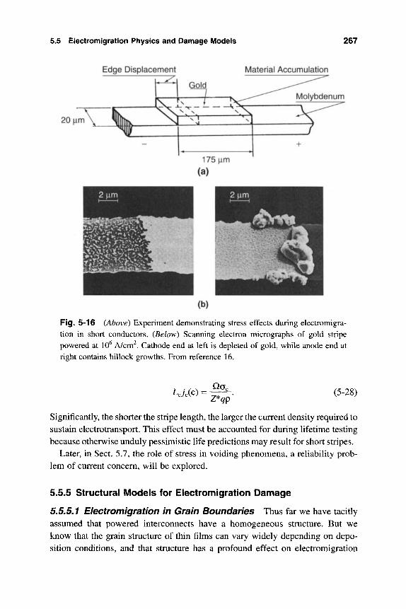
5.5 Electromigration Physics and Damage Models 267
Edge Displacement Material Accumulation
20|im
Fig. 5-16 (Above) Experiment demonstrating stress effects during electromigra-tion in short conductors. (Below) Scanning electron micrographs of gold stripe powered at 10 A/cm . Cathode end at left is depleted of gold, while anode end at right contains hillock growths. From reference 16.
^c7e(c) = (5-28)
Significantly, the shorter the stripe length, the larger the current density required to sustain electrotransport. This effect must be accounted for during lifetime testing because otherwise unduly pessimistic life predictions may result for short stripes.
Later, in Sect. 5.7, the role of stress in voiding phenomena, a reliability prob-lem of current concern, will be explored.
5.5.5 Structural Models for Electromigration Damage
5.5,5.1 Electromigration in Grain Boundaries Thus far we have tacitly assumed that powered interconnects have a homogeneous structure. But we know that the grain structure of thin films can vary widely depending on depo-sition conditions, and that structure has a profound effect on electromigration
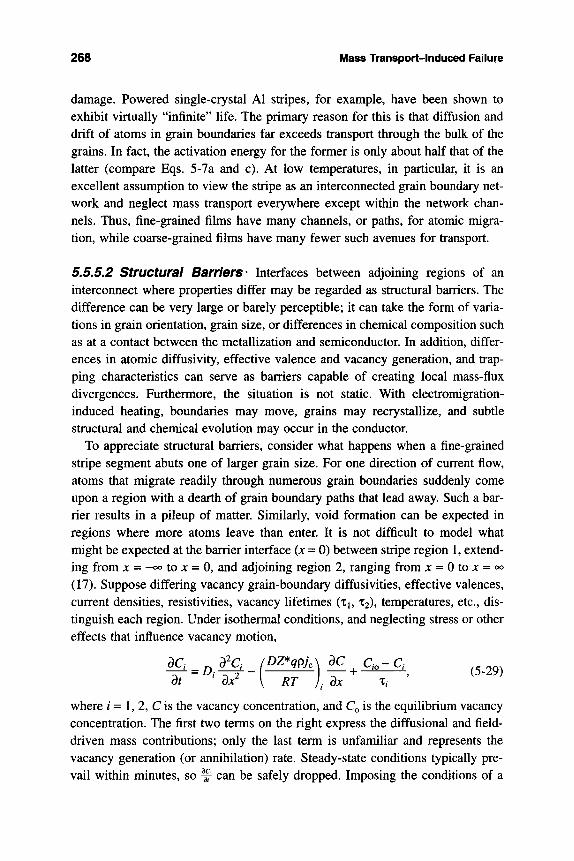
268 Mass Transport-Induced Failure
damage. Powered single-crystal Al stripes, for example, have been shown to exhibit virtually "infinite" life. The primary reason for this is that diffusion and drift of atoms in grain boundaries far exceeds transport through the bulk of the grains. In fact, the activation energy for the former is only about half that of the latter (compare Eqs. 5-7a and c). At low temperatures, in particular, it is an excellent assumption to view the stripe as an interconnected grain boundary net-work and neglect mass transport everywhere except within the network chan-nels. Thus, fine-grained films have many channels, or paths, for atomic migra-tion, while coarse-grained films have many fewer such avenues for transport.
5.5,5.2 Structural Barriers \ Interfaces between adjoining regions of an interconnect where properties differ may be regarded as structural barriers. The difference can be very large or barely perceptible; it can take the form of varia-tions in grain orientation, grain size, or differences in chemical composition such as at a contact between the metallization and semiconductor. In addition, differ-ences in atomic diffusivity, effective valence and vacancy generation, and trap-ping characteristics can serve as barriers capable of creating local mass-flux divergences. Furthermore, the situation is not static. With electromigration-induced heating, boundaries may move, grains may recrystallize, and subtle structural and chemical evolution may occur in the conductor.
To appreciate structural barriers, consider what happens when a fine-grained stripe segment abuts one of larger grain size. For one direction of current flow, atoms that migrate readily through numerous grain boundaries suddenly come upon a region with a dearth of grain boundary paths that lead away. Such a bar-rier results in a pileup of matter. Similarly, void formation can be expected in regions where more atoms leave than enter. It is not difficult to model what might be expected at the barrier interface (x = 0) between stripe region 1, extend-ing from jc = -oo to X = 0, and adjoining region 2, ranging from jc = 0 to jc = oo (17). Suppose differing vacancy grain-boundary diffusivities, effective valences, current densities, resistivities, vacancy lifetimes (Xi, T2), temperatures, etc., dis-tinguish each region. Under isothermal conditions, and neglecting stress or other effects that influence vacancy motion.
A ^ - I SZ I — + ^"^V^^ (5-29) dt ' 3 / [ RT ) . dx T,
where / = 1, 2, C is the vacancy concentration, and Q is the equilibrium vacancy concentration. The first two terms on the right express the diffusional and field-driven mass contributions; only the last term is unfamiliar and represents the vacancy generation (or annihilation) rate. Steady-state conditions typically pre-vail within minutes, so ^ can be safely dropped. Imposing the conditions of a
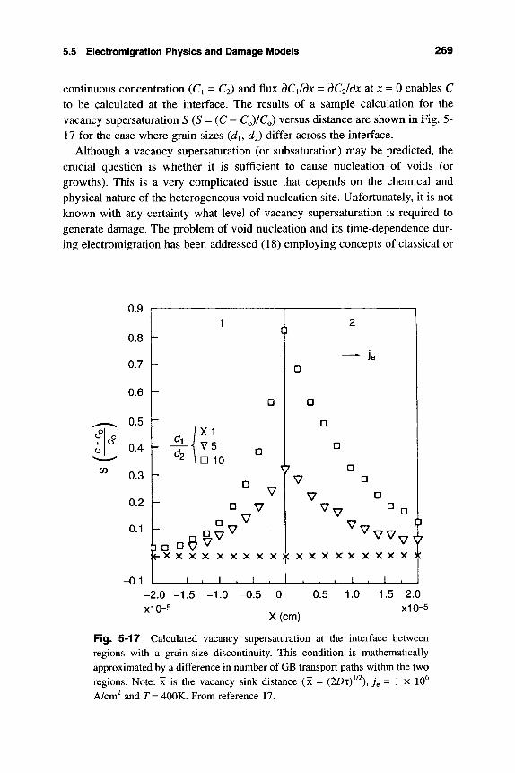
5.5 Electromigration Physics and Damage Models 269
continuous concentration (Ci = C^) and flux dCildx = dC2/dx at x = 0 enables C to be calculated at the interface. The results of a sample calculation for the vacancy supersaturation S (S = (C- C^ICQ) versus distance are shown in Fig. 5-17 for the case where grain sizes (Ji, d^) differ across the interface.
Although a vacancy supersaturation (or subsaturation) may be predicted, the crucial question is whether it is sufficient to cause nucleation of voids (or growths). This is a very complicated issue that depends on the chemical and physical nature of the heterogeneous void nucleation site. Unfortunately, it is not known with any certainty what level of vacancy supersaturation is required to generate damage. The problem of void nucleation and its time-dependence dur-ing electromigration has been addressed (18) employing concepts of classical or
c/5
-0.1 -2.0 -1.5 -1.0 -0.5 xlO-5
0
X(cm)
0.5 1.0 1.5 2.0 xlO-5
Fig. 5-17 Calculated vacancy supersaturation at the interface between regions with a grain-size discontinuity. This condition is mathematically approximated by a difference in number of GB transport paths within the two regions. Note: x is the vacancy sink distance (x = {IDx)^'^), j^ = 1 x 10 A/cm^ and 7= 400K. From reference 17.
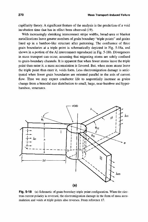
270 Mass Transport-Induced Failure
capillarity theory. A significant feature of the analysis is the prediction of a void
incubation time that has in effect been observed (19). With increasingly shrinking interconnect stripe widths, broad-area or blanket
metallizations leave greater numbers of grain boundary "triple points" and grains hned up in a bamboo-like structure after patterning. The confluence of three grain boundaries at a triple point is schematically depicted in Fig. 5-18a, and shown in a portion of the Al interconnect reproduced in Fig. 5-18b. Divergences in mass transport can occur, assuming that migrating atoms are solely confined to grain-boundary channels. It is apparent that when fewer atoms leave the tnple point than enter it, a mass accumulation is favored. But, when more atoms leave the triple point than enter it, voids form. Less electromigration damage is antic-ipated when fewer grain boundaries are oriented parallel to the axis of current flow Thus we may expect conductor Ufe to sequentially increase as grams change from a bimodal size distribution to small, large, near-bamboo and hyper-bamboo, structures.
Fig 5-18 (a) Schematic of grain-boundary triple point configuration. When the elec-tron current polarity is reversed, the electromigration damage in the form of mass accu-mulation and voids at triple points also reverses. From reference 17.
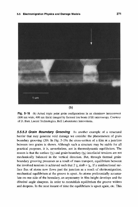
5.5 Electromigration Physics and Damage Models 271
Fig. 5-18 (b) Actual triple point grain configurations in an aluminum interconnect (800 nm wide, 400 nm thick) imaged by focused ion beam (FIB) microscopy. Courtesy of D. Barr, Lucent Technologies, Bell Laboratories Innovations.
5.5.5.3 Grain Boundary Grooving As another example of a structural barrier that may generate void damage we consider the phenomenon of grain boundary grooving (20). In Fig. 5-19a the cross-section of a film at a junction between two grains is shown. Although such a structure may be stable for all practical purposes, it is, nevertheless, not in thermodynamic equilibrium. The reason is that the surface (YS) and grain-boundary (yt) interfacial tensions are not mechanically balanced in the vertical direction. But, through thermal grain-boundary grooving processes as a result of mass transport, equilibrium between the involved tensions is achieved such that 2 YS sinO = y^. If a unidirectional sur-face flux of atoms now flows past the junction as a result of electromigration, mechanical equilibrium at the groove is upset. As atoms preferentially accumu-late on one side of the boundary, an asymmetry in film height develops and the dihedral angle sharpens. In order to reestablish equilibrium the groove widens and deepens. In the next instant of time the equilibrium is upset again, etc. This
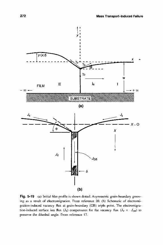
272 Mass Transport-Induced Failure
(b)
Fig. 5-19 (a) Initial film profile is shown dotted. Asymmetric grain-boundary groov-ing as a result of electromigration. From reference 20. (b) Schematic of electromi-gration-induced vacancy flux at grain-boundary (GB) triple point. The electromigra-tion-induced surface ion flux (7s) compensates for the vacancy flux (/y = --^GB) to preserve the dihedral angle. From reference 17.
5.6 Electromigration in Practice 273
perpetual drive to equilibrium punctuated by intermediate moments of instabil-ity ultimately causes the groove to reach the substrate where a void or open cir-cuit is produced. Such a mechanism occurs at any level of vacancy supersatura-tion, in contrast to the damage model presented in Sect. 5.5.5.2. Analytical expressions for the kinetics of grooving and surface topography of the grains have been published.
Finally, we may consider grooving to cause damage at a grain-boundary triple point by an electromigration-induced vacancy flux, as shown in Fig. 5-19b. This case has been modeled (17), and the length (y) of the grain-boundary hole pro-duced as a function of time (0 is given by
^ _ M ^ ^ (5-30)
where M = C^bD^*q il2vj)jl%, B = D^y^ VsQ /kT, and T is the ganmia func-tion. In these expressions b refers to the grain boundary, s to the surface; Vg is the effective surface ion concentration, and Q is the atomic volume. Times calcu-lated to produce damage are of the order of tens of hours for reasonable choices of the involved constants.
5.6 ELECTROiy/IIGRATION IN PRACTICE
5.6.1 Manifestations of Eiectromigration Damage
All powered metals in integrated circuits are potentially susceptible to electro-migration effects. Interconnects, contacts, and vias are the three locations that are particularly prone to damage. Much of Sect. 5.5 was devoted to degradation and failure in interconnections; this discussion is by no means over and will con-tinue. We start by discussing electromigration-damage manifestations in contacts and vias.
5.6.1.1 Electromigration at Contacts Large mass divergences are expect-ed at powered contacts because any metal that leaves the semiconductor inter-face cannot be replenished. The subject of diffusional degradation at contacts in both Si and GaAs devices was treated earlier. However, in the presence of simul-taneous electromigration, the damage accelerates. Ondrusek et ah (21) have studied the wearout of both Al~Si and TiSi2-Si contacts and found the latter to be considerably less susceptible to electromigration degradation. For the case of
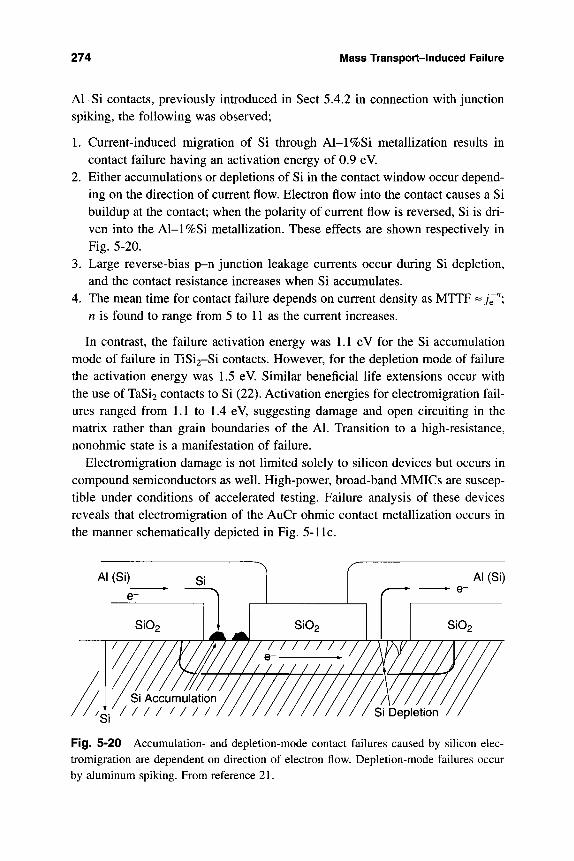
274 Mass Transport-Induced Failure
Al-Si contacts, previously introduced in Sect 5.4.2 in connection with junction spiking, the following was observed;
1. Current-induced migration of Si through Al-l%Si metallization results in contact failure having an activation energy of 0.9 eV.
2. Either accumulations or depletions of Si in the contact window occur depend-ing on the direction of current flow. Electron flow into the contact causes a Si buildup at the contact; when the polarity of current flow is reversed. Si is dri-ven into the Al-l%Si metallization. These effects are shown respectively in Fig. 5-20.
3. Large reverse-bias p-n junction leakage currents occur during Si depletion, and the contact resistance increases when Si accumulates.
4. The mean time for contact failure depends on current density as MTTF ~7e"; n is found to range from 5 to 11 as the current increases.
In contrast, the failure activation energy was 1.1 eV for the Si accumulation mode of failure in TiSi2-Si contacts. However, for the depletion mode of failure the activation energy was 1.5 eV. Similar beneficial life extensions occur with the use of TaSi2 contacts to Si (22). Activation energies for electromigration fail-ures ranged from 1.1 to 1.4 eV, suggesting damage and open circuiting in the matrix rather than grain boundaries of the Al. Transition to a high-resistance, nonohmic state is a manifestation of failure.
Electromigration damage is not limited solely to silicon devices but occurs in compound semiconductors as well. High-power, broad-band MMICs are suscep-tible under conditions of accelerated testing. Failure analysis of these devices reveals that electromigration of the AuCr ohmic contact metallization occurs in the manner schematically depicted in Fig. 5-lie.
Fig. 5-20 Accumulation- and depletion-mode contact failures caused by silicon elec-tromigration are dependent on direction of electron flow. Depletion-mode failures occur by aluminum spiking. From reference 21.
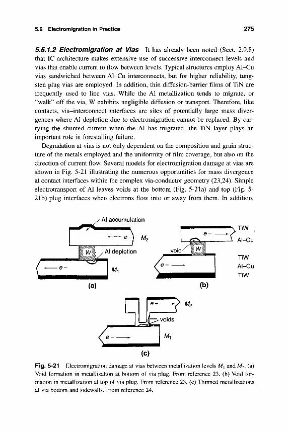
5.6 Electromigration in Practice 275
5.6.1.2 Electromigration at Vias It has already been noted (Sect. 2.9.8) that IC architecture makes extensive use of successive interconnect levels and vias that enable current to flow between levels. Typical structures employ Al-Cu vias sandwiched between Al-Cu interconnects, but for higher reliability, tung-sten plug vias are employed. In addition, thin diffusion-barrier films of TiN are frequently used to line vias. While the Al metallization tends to migrate, or "walk" off the via, W exhibits negligible diffusion or transport. Therefore, like contacts, via-interconnect interfaces are sites of potentially large mass diver-gences where Al depletion due to electromigration cannot be replaced. By car-rying the shunted current when the Al has migrated, the TiN layer plays an important role in forestalling failure.
Degradation at vias is not only dependent on the composition and grain struc-ture of the metals employed and the uniformity of film coverage, but also on the direction of current flow. Several models for electromigration damage at vias are shown in Fig. 5-21 illustrating the numerous opportunities for mass divergence at contact interfaces within the complex via-conductor geometry (23,24). Simple electrotransport of Al leaves voids at the bottom (Fig. 5-2la) and top (Fig. 5-21b) plug interfaces when electrons flow into or away from them. In addition.
Fig. 5-21 Electromigration damage at vias between metallization levels Mj and M2. (a) Void formation in metallization at bottom of via plug. From reference 23. (b) Void for-mation in metallization at top of via plug. From reference 23. (c) Thinned metallizations at via bottom and side walls. From reference 24.
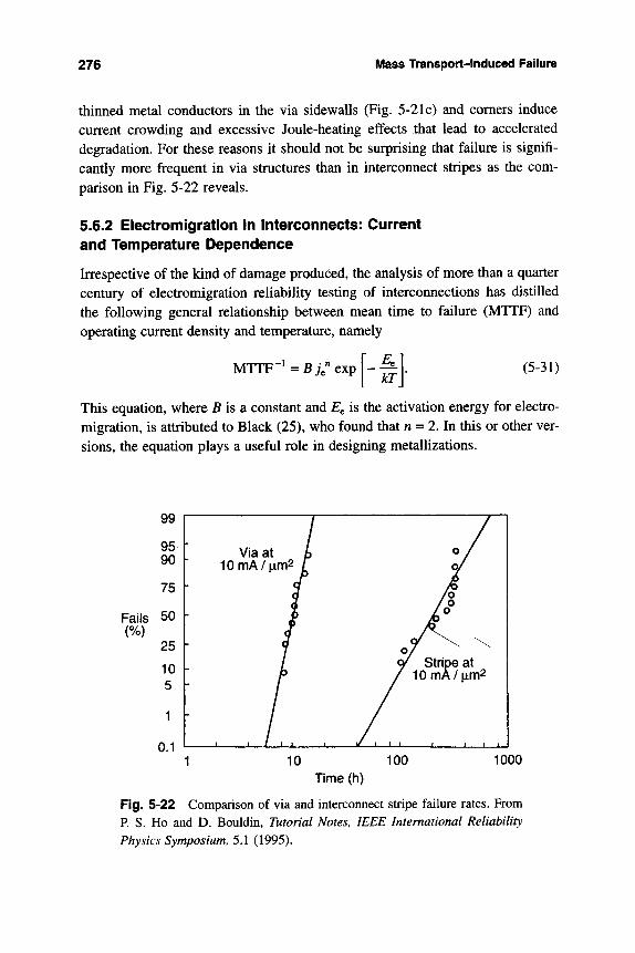
276 Mass Transport-Induced Failure
thinned metal conductors in the via sidewalls (Fig. 5-2 Ic) and comers induce current crowding and excessive Joule-heating effects that lead to accelerated degradation. For these reasons it should not be surprising that failure is signifi-cantly more frequent in via structures than in interconnect stripes as the com-parison in Fig. 5-22 reveals.
5.6.2 Electromigration in Interconnects: Current and Temperature Dependence
Irrespective of the kind of damage produced, the analysis of more than a quarter century of electromigration reliability testing of interconnections has distilled the following general relationship between mean time to failure (MTTF) and operating current density and temperature, namely
MTTF"^=57e"exp m (5-31)
This equation, where 5 is a constant and E^ is the activation energy for electro-migration, is attributed to Black (25), who found that n = 2. In this or other ver-sions, the equation plays a useful role in designing metallizations.
99
95 90 h
75
Fails 50 (%)
25
10 5
0.1
Via at 10mA/|Lim2
100 1000 Time (h)
Fig. 5-22 Comparison of via and interconnect stripe failure rates. From P. S. Ho and D. Bouldin, Tutorial Notes, IEEE International Reliability Physics Symposium, 5.1 (1995)*
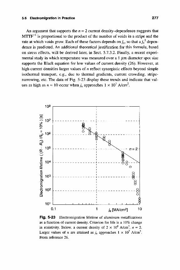
5.6 Electromigration in Practice 277
An argument that supports then = 2 current density-dependence suggests that MTTF"^ is proportional to the product of the number of voids in a stripe and the rate at which voids grow. Each of these factors depends onj^, so that a g^ depen-dence is predicted. An additional theoretical justification for this formula, based on stress effects, will be derived later, in Sect. 5.7.3.2. Finally, a recent experi-mental study in which temperature was measured over a 1 (iim diameter spot size supports the Black equation for low values of current density (26). However, at high current densities larger values of n reflect synergistic effects beyond simple isothermal transport, e.g., due to thermal gradients, current crowding, stripe-narrowing, etc. The data of Fig. 5-23 display these trends and indicate that val-ues as high as n ~ 10 occur whenjg approaches 1 x 10^ A/cm^.
7e [MA/cm2]
Fig. 5-23 Eleetromigration lifetime of aluminum metallizations as a function of current density. Criterion for life is a 10% change in resistivity. Below, a current density of 2 x 10 A/cm , n = 2. Larger values of n are attained as j^ approaches 1 x 10 AJcvo?. From reference 26.
278 Mass Transport-Induced Failure
The thermally activated nature of electromigration damage is underscored by Eq. 5-31. It is important to realize, however, that E^ and n values extracted from lifetime testing, resistance monitoring, or other indirect measurements typically reflect a complex admixture of mass transport and damage processes: void nucleation, migration and coalescence, grain-boundary diffu-sion, surface diffusion, stress-assisted diffusion, thermomigration, grooving, extrusion and so on. Increasing current densities enhance these processes in a nonlinear fashion. It is little wonder then that hot spots develop to further accelerate failure.
The range of activation energy values typically measured in assorted metal films used in electronics technology are entered in Table 5-1. Corresponding composition and grain size ranges employed are also listed. For more detailed information on the more than 60 studies from which the representative compos-ite values of E^ were selected, the reader should consult the indicated reference. The overwhelming bulk of the data pertains to Al and Al alloy metallizations, where the following observations apply:
1. The activation energy for bulk diffusion in pure Al is 1.4 eV. For films with large grain size there are few avenues for defect diffusion paths, and thus E^ is found to be 1 to 1.2 eV. However, measured E^ values in the neighborhood of 0.4-0.6 eV for the usual fine-grained films are indicative of grain bound-ary mass transport-induced damage. Observed grain-size-dependent activa-tion energies are the apparent consequence of weighting admixtures of low bulk and high grain-boundary diffusivity contributions.
2. Additions of Cu to Al raise E^ by a few tenths of an eV and extend MTTF lifetimes of Al accordingly. This important finding is the basis for the use of Al alloy metallizations containing -0.3 to 5 wt.% Cu. The effect of Cu is not
Table 5-1 Electromigration in Metal Films
Metal
Pure Al
Al-0.3 to 5 wt%Cu Al-0.3 to 3 wt%Si Al-Cu-Si Au
Ag Cu
Grain size
0.1 to 2 6 to 8 1 to 6 0.3 to 7.6 0.25 to 0.6 0.2 to 0.5
(^im) Failure criteria
A/?//?, open circuit
A/?//?, open circuit JSR/R, open circuit A/?/R, open circuit A/?//?, open circuit, tracer,
E, (eV)
0.35 to -0.6 1.0 to 1.2 0.5 to 0.8 0.31 to 0.8 0.25 to 0.86 0.7 to 0.9
n
2 to 4
2 1.7 to 5.4 1.7 3.3 to 4
0.3 to 0.95 1.1
Primarily adapted from A. Scorzoni, B. Neri, C. Caprile, and F. Fantini, Materials Science Reports 7, 143 (1991).
5.6 Electromigration in Practice 279
completely understood, but the AI2CU precipitates and dissolved Cu appear to interact with Al atoms in grain boundaries and impede their motion. (In com-mercial Al-Cu precipitation hardening alloys these same AI2CU precipitates strengthen the Al matrix.) It is also common to add 1 wt.% Si as well to pre-vent Al-Si interdiffusion at semiconductor contacts.
3. The activation energy values are in general agreement with the diffusivity systematics presented in Eq. 5-7. Thus E^ scales directly with higher melting point and larger grain size.
5.6.3 Effect of Conductor Geometry and Grain Structure on Electromigration
The dependence of conductor length and width on electromigration life has been a subject of continuing interest. Assuming constant width, longer stripes simply have more potential failure sites (e.g., triple points) than shorter conductors, and therefore, they are observed to exhibit reduced lifetimes. But, when stripes are unusually short, stress-induced mass backflow effects (Sect. 5.5.4) surface to counter electromigration damage.
From the earlier discussion of structural barriers (Sect. 5.5.5.2) the desirabil-ity of having equiaxed grains is evident. Even better than equiaxed grains are interconnects with no grain boundaries, i.e., a single-crystal Al film. Since it is impractical to deposit such a film, the best alternative is an interconnect with a bamboo grain structure that effectively behaves like a series stack of single crys-tals. The GBs are then oriented normal to the current flow. In such a case the only path available for mass transport is through the bulk grains, an unlikely avenue at low temperature. From a geometric standpoint, shrinking line dimen-sions make bamboo structures more probable. Interestingly, the effect of decreasing film linewidths on electromigration failure time reveals an unex-pected beneficial twist, as revealed in Fig. 5-24. Film life decreases as the linewidth is reduced from 4 |xm to 2 |xm, in accord with intuitive expectations that the narrower the stripe, the easier it is for damage to span across it. How-ever, an encouraging increase in life occurs below 2 jiim because of the bamboo grain development (27).
From the standpoint of processing, the film lifetime seems to be affected by method of film deposition; evaporated films are apparently longer lived than sputtered films, a fact perhaps attributable to a more random crystallographic texture in the case of the latter. Multiple GB orientations thus appear to encour-age electrotransport damage effects. A suggested formula that neatly summarizes the dependence of mean lifetime on grain size (5*), the standard deviation statis-tical spread in grain size (Ogs), and the preferred crystallographic orientation is
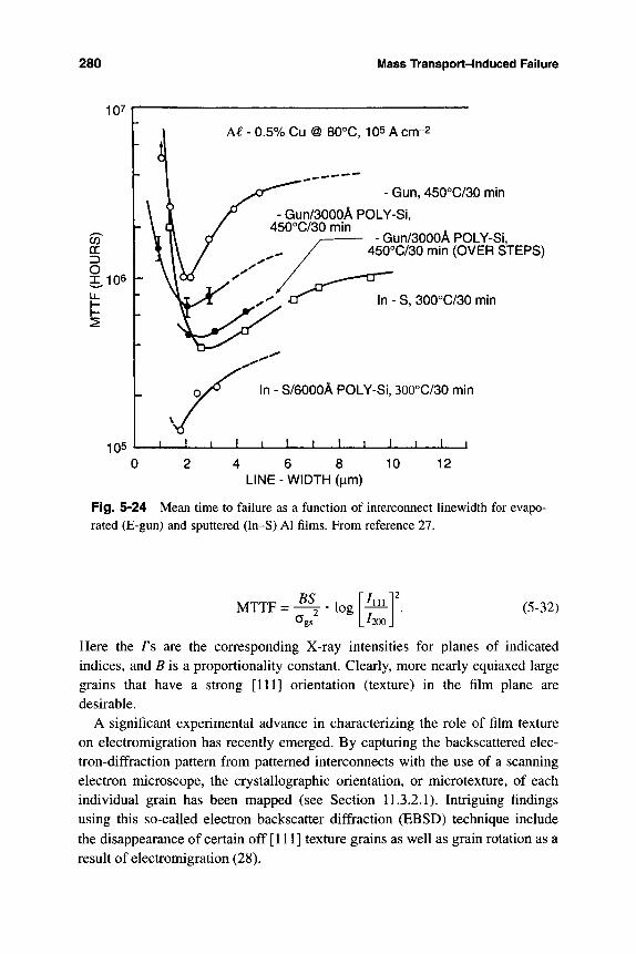
280 Mass Transport-Induced Failure
107
CO
cc o ^ X 106
105
A€ - 0.5% Cu @ 80°C, 105 A cm-2
- Gun, 450°C/30 min
- Gun/3000A POLY-Si, 450°C/30 min
- Gun/SOOOA POLY-Si, 450°C/30 min (OVER STEPS)
In - S, 300°C/30 min
In - S/eOOOA POLY-Si, 300°C/30 min
t I I I 1 I I i I I I
4 6 8 10 LINE - WIDTH (^m)
12
Fig. 5-24 Mean time to failure as a function of interconnect linewidth for evapo-rated (E-gun) and sputtered (In-S) Al films. From reference 27.
MTTF = BS
-'gs
log / i l l 12
200 (5-32)
Here the /'s are the corresponding X-ray intensities for planes of indicated indices, and ^ is a proportionality constant. Clearly, more nearly equiaxed large grains that have a strong [111] orientation (texture) in the film plane are desirable.
A significant experimental advance in characterizing the role of film texture on electromigration has recently emerged. By capturing the backscattered elec-tron-diffraction pattern from patterned interconnects with the use of a scanning electron microscope, the crystallographic orientation, or microtexture, of each individual grain has been mapped (see Section 11.3.2.1). Intriguing findings using this so-called electron backscatter diffraction (EBSD) technique include the disappearance of certain off [111] texture grains as well as grain rotation as a result of electromigration (28).
5.6 Electromigration in Practice 281
5.6.4 Electromigration Lifetime Distributions
Eleetromigration failure times are invariably modeled as lognormal distributions. Examples of electromigration failure data plotted in lognormal form are shown in Fig. 5-25. There are two physical reasons that explain why this particular statistical function is applicable to electromigration failures. The first has to do with profusion of damage mechanisms exhibited. As a result of the suggestion in Sect. 4.5.4 we may assume that electromigration exhibits a corresponding number of randomly distributed activation energies. But since failure times are directly proportional to the Maxwell-Boltzmann factor, exp [- EJkT], the logarithm yields EJkT, which is normally distributed. Hence the overall use of the lognormal distribution.
A second explanation justifying the applicability of the lognormal distribution is based on the temperature dispersion of conductors during hfe testing (29). Due to the different thermal resistance values, individual stripe temperatures are nor-mally distributed. Given the Black equation's exponential dependence on tem-perature, a lognormal distribution of failure times would be expected.
Another approach to the statistics of interconnect reliability adopts the view that a metal stripe is a chain of N independent links such that F{t) is the cumu-lative distribution function (CDF) of a single link (30). The scaled CDF of the chain, F^(0» is then the strength distribution of the "weakest link," or
f W ( 0 = l - [ l - / ^ O f . (5-33)
Simple substitution of the Weibul form of F{t) reveals that Ff^t) is also a WeibuU distribution. Nevertheless, attempts to fit large failure populations to such a self-reproducing WeibuU function have proven unsuccessful (31). But if F{i) is lognormal, F^O is not lognormal. The conclusion is that lognormal dis-tributions can lapproximate true failure times only in a finite percentile interval. Furthermore, what characterizes the length of the weak link is not clear. Is it, for example, the grain size or perhaps the threshold length, L^l
5.6.5 Eiectromigration Testing
Irrespective of degradation mechanism, it is always a desideratum to accelerate testing in order to rapidly screen production lots prone to failure. In the case of electromigration several test methods have gained popularity. Each has individ-ual advantages and drawbacks, but in common fast response (minutes to a few hours at most) and scaleup to the wafer level are sought-after features. By wafer level we mean placing a pair of probes across any interconnect prior to separa-tion into dies. In this section three of these tests are briefly described.
The first test is known as the temperature-ramp resistance analysis to charac-terize electromigration, or TRACE (32). In this test a temperature (7) vs time (t)
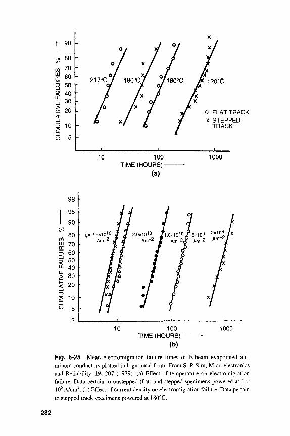
1
CO LU
D - J < II LU
> 1-< - J 3
3 O
90
80
70 60 SO 40 30 20
10
b
120°C
10 100 TIME (HOURS)-
(a)
0 FLAT TRACK X STEPPED
TRACK
1000
98
95
90
80 CO S 70 5 60 i 50 ^ 40 LU > 30 ! 20 _ j 3 ^ 10 D ^ 5
- Je= 2.5x1 ( Am
10 100 TIME (HOURS)-
(b)
1000
Fig. 5-25 Mean electromigration failure times of E-beam evaporated alu-minum conductors plotted in lognormal form. From S. P. Sim, Microelectronics and Reliability, 19, 207 (1979). (a) Effect of temperature on electromigration failure. Data pertain to unstepped (flat) and stepped specimens powered at 1 x 10^ A/cm^. (b) Effect of current density on electromigration failure. Data pertain to stepped track specimens powered at 180°C.
282
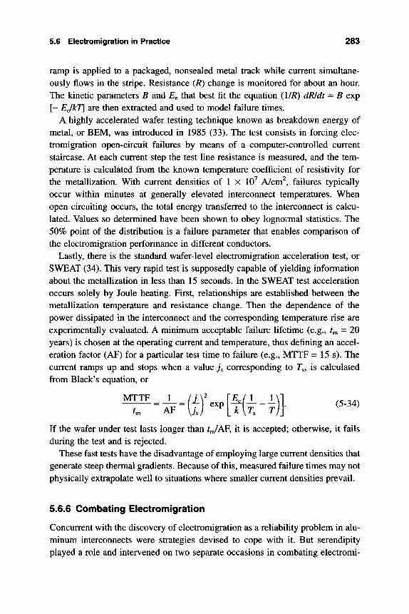
5.6 Electromigration in Practice 283
ramp is applied to a packaged, nonsealed metal track while current simultane-ously flows in the stripe. Resistance (R) change is monitored for about an hour. The kinetic parameters B and E^ that best fit the equation (l/R) dRJdt = B exp [- EJkT] are then extracted and used to model failure times.
A highly accelerated wafer testing technique known as breakdown energy of metal, or BEM, was introduced in 1985 (33). The test consists in forcing elec-tromigration open-circuit failures by means of a computer-controlled current staircase. At each current step the test line resistance is measured, and the tem-perature is calculated from the known temperature coefficient of resistivity for the metallization. With current densities of 1 x 10^ A/cm^, failures typically occur within minutes at generally elevated interconnect temperatures. When open circuiting occurs, the total energy transferred to the interconnect is calcu-lated. Values so determined have been shown to obey lognoiinal statistics. The 50% point of the distribution is a failure parameter that enables comparison of the electromigration performance in different conductors.
Lastly, there is the standard wafer-level electromigration acceleration test, or SWEAT (34). This very rapid test is supposedly capable of yielding information about the metallization in less than 15 seconds. In the SWEAT test acceleration occurs solely by Joule heating. First, relationships are established between the metallization temperature and resistance change. Then the dependence of the power dissipated in tiie interconnect and the corresponding temperature rise are experimentally evaluated. A minimum acceptable failure lifetime (e.g., t^ = 20 years) is chosen at the operating current and temperature, thus defining an accel-eration factor (AF) for a particular test time to failure (e.g., MTTF = 1 5 s). The current ramps up and stops when a value j^ corresponding to T , is calculated from Black's equation, or
MTTF ^ J _ ^ (j}^ ^^ (5-34)
If the wafer under test lasts longer than t^JAF, it is accepted; otherwise, it fails during the test and is rejected.
These fast tests have the disadvantage of employing large current densities that generate steep thermal gradients. Because of this, measured failure times may not physically extrapolate well to situations where smaller current densities prevail,
S.6.6 Combating Electromigration
Concurrent with the discovery of electromigration as a reliability problem in alu-minum interconnects were strategies devised to cope with it. But serendipity played a role and intervened on two separate occasions in combating electromi-
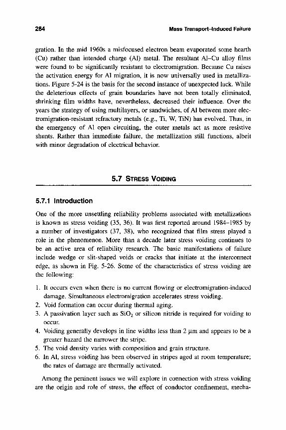
284 Mass Transport-Induced Failure
gration. In the mid 1960s a misfocused electron beam evaporated some hearth (Cu) rather than intended charge (Al) metal. The resuhant Al-Cu alloy films were found to be significantly resistant to electromigration. Because Cu raises the activation energy for Al migration, it is now universally used in metalliza-tions. Figure 5-24 is the basis for the second instance of unexpected luck. While the deleterious effects of grain boundaries have not been totally eliminated, shrinking film widths have, nevertheless, decreased their influence. Over the years the strategy of using multilayers, or sandwiches, of Al between more elec-tromigration-resistant refractory metals (e.g., Ti, W, TiN) has evolved. Thus, in the emergency of Al open circuiting, the outer metals act as more resistive shunts. Rather than immediate failure, the metallization still functions, albeit with minor degradation of electrical behavior.
5.7 STRESS VOIDING
5.7.1 Introduction
One of the more unsettling reliability problems associated with metallizations is known as stress voiding (35, 36). It was first reported around 1984-1985 by a number of investigators (37, 38), who recognized that film stress played a role in the phenomenon. More than a decade later stress voiding continues to be an active area of reliability research. The basic manifestations of failure include wedge or slit-shaped voids or cracks that initiate at the interconnect edge, as shown in Fig. 5-26. Some of the characteristics of stress voiding are the following:
1. It occurs even when there is no current flowing or electromigration-induced damage. Simultaneous electromigration accelerates stress voiding.
2. Void formation can occur during thermal aging. 3. A passivation layer such as Si02 or silicon nitride is required for voiding to
occur. 4. Voiding generally develops in line widths less than 2 |im and appears to be a
greater hazard the narrower the stripe. 5. The void density varies with composition and grain structure. 6. In Al, stress voiding has been observed in stripes aged at room temperature;
the rates of damage are thermally activated.
Among the pertinent issues we will explore in connection with stress voiding are the origin and role of stress, the effect of conductor confinement, mecha-
5.7 Stress Voiding 285
Slit Void
f^^-'^-^Jl^^p* Void and Hillock
Mtwm.. -5,, ,t u,v MS. «:*:k' *i: %¥, ft.
Edge Void
Fig. 5-26 SEM images of stress-related electromi-gration damage in Al interconnects. Top. Wedge or slit void in a 0.8 jim wide stripe. Middle. Void and hillock formation in a 1 |im wide stripe. Bottom. Edge void. Courtesy of M. Marcus, Lucent Technologies, Bel] Laboratories Innovations.
nisms for mass transport-induced damage, and the optimization of materials and processing for improved reliability. We start with stress effect considerations.
5.7.2 Origin of Stress in l\/letallizations
It is instructive to start with Fig. 5-27, which summarizes the state of stress in metal films for different material and geometric configurations (39). The blanket, unpassivated thin film deposited on a substrate in Fig. 5-27a is under a balanced
286 Mass Transport-Induced Failure
Thin blanket film Unpassivated line
Isotropic biaxial stress Unequal biaxial stress
Passivated line
Triaxial stress
Fig. 5-27 States of stress in metal films. From P. S. Ho and D. Bouldin, Tutorial Notes, IEEE International Relia-bility Physics Symposium, 5.1 (1995). (a) Blanket, unpassi-vated thin metal film (a^ = Cy, a = 0). (b) Patterned, unpas-sivated narrow metal stripe (G^ "^ Oy, 0^ = 0). (c) Metal stripe is passivated by blanket insulator film (a^ Cy^ a , a 0).
biaxial stress distribution, i.e., 0^= Oy. But, because of the stress-free surface, a^ = 0. As noted in Sect. 3.3.2, film stress stems from the thermal mismatch between film and substrate as well as from the detailed mechanics of growth. For a wide stripe, a balanced biaxial stress distribution still prevails for the most part. However, if the film is in the form of a narrow stripe (Fig. 5-27b), then near the lateral edges of the film c^ does not equal Cy, but one still expects that a^ = 0. If now this narrow line is encompassed by an overlying passivating thin film (Fig. 5-27c), an unbalanced triaxial state of stress (i.e., c^Cy^ G^) will develop.
The thermal origins of these stresses allow for a rough estimate of their magni-tudes. For the case of Al, passivated by Si3N4 deposited at elevated temperature, the metal contracts more than the nitride upon cooling. Therefore, the Al is stressed in tension and the Si3N4 in compression. Provided that a stress-free state exists at the passivation deposition temperature (7), use of Eq. 3-8 enables the stress in the Al to be calculated at the use temperature T^, Assuming T - TQ = 300°C, £(A1) = 69 GPa, v (Al) = 0.33, oCf (Al) = 25 x 10"^ °C"\ and a, {Si^^^) = 2.5 X 10"^ °C~\ the calculated thermal stress in the metal is a = + 0.695 GPa. Such a level is well above the tensile yield stress of Al alloys, and therefore we may
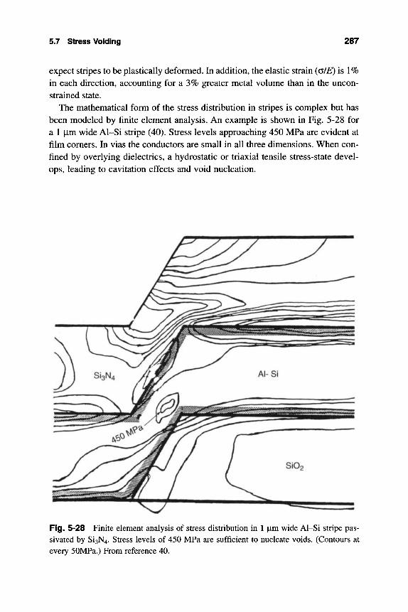
5.7 Stress Voiding 287
expect stripes to be plastically deformed. In addition, the elastic strain (a/£) is 1% in each direction, accounting for a 3% greater metal volume than in the uncon-strained state.
The mathematical form of the stress distribution in stripes is complex but has been modeled by finite element analysis. An example is shown in Fig. 5-28 for a 1 jim wide Al-Si stripe (40). Stress levels approaching 450 MPa are evident at film comers. In vias the conductors are small in all three dimensions. When con-fined by overlying dielectrics, a hydrostatic or triaxial tensile stress-state devel-ops, leading to cavitation effects and void nucleation.
Fig. 5-28 Finite element analysis of stress distribution in 1 jxm wide Al-Si stripe pas-sivated by Si3N4. Stress levels of 450 MPa are sufficient to nucleate voids. (Contours at every 50MPa.) From reference 40.
288 Mass Transport-Induced Failure
5.7.3 Vacancies, Stresses, Voids, and Failure
5.7.3.1 Void Nucleation This section attempts to explore the suggested Hnkage among vacancies, stresses, and voids, as well as to forge connections between electromigration, stress voiding, and failure. We start this ambitious undertaking by noting that for reasons given in Sect. 5.7.2, passivated intercon-nects are observed to contain grain-boundary voids when cooled to room tem-perature. According to classical nucleation theory, a spherical void of radius r is stable when the strain (free) energy reduction in forming it exceeds the energy increase associated with creating new void surface area. Furthermore, according to thermodynamics, atoms have different "effective" atomic concentrations depending on their chemical potentials (\x). Thus, when atoms lie within stressed regions |x = - a Q (see Sect. 5.5.4), while on curved (void) surfaces |i = 2 yQ,/r, where y is the surface energy (J/m^). If the potentials are equal at equilibrium, r = 2y/a. For y = 1 J/m^ and a = 400 MPa, a void of radius 5 nm is stable. Importantly, stressed regions and voids modify vacancy concentrations (Eq. 3-1) by altering their (free) energy of formation.
5.7.3.2 Atom Transport under Electromigration and Stress Forces Directed atom (or vacancy) transport from stressed grain boundaries, disloca-tions, interfaces, etc. to voids, or vice versa, under gradients in the chemical potential (V|LI) is responsible for enlargement or shrinkage of voids. Atomic drift preferentially occurs from locations of higher chemical potential to those of lower chemical potential. To develop a quantitative macroscopic model of stress-driven atom (vacancy) flow, we recall that the force on an atom in a stress field is given by F=Q. da /dx (Eq. 5-26). When this stress-induced force is added to the primary electric field driving force, substitution in the Nemst-Einstein equa-tion yields
CD
~ RT Z*qp7e + Q ^ | . (5-35)
Interconnect damage occurs under isothermal conditions when the divergence of the mass flux,
dt dx Z*^P7e + ^ - ^
RT\ ^ dx (5-36)
is nonzero. Changes in atomic concentration cause stress variations and vice versa. Therefore, dC/dt is proportional to dc/dt, and it has been specifically shown that dC/dt = -(C/B) do/dt, where B is an appropriate constant with a value equal to ~ 0.6 times Young's modulus (41). Substituting yields
5.7 Stress Voiding 289 stress Voiding
da dt
d dx
rDBQ
RT dx a I (5-37)
These last two equations form the basis of interrelated mass or vacancy transport and change in film stress in the presence of electromigration. According to them the current-induced vacancy flux creates a stress-directed counterflux that retards electromigration damage.
We now consider the Fick-like diffusion portion of Eq. 5-37,
dt RT dx^ (5-38)
and note that stress changes can be expected over a long period with a charac-teristic time given by an effective diffusion coefficient equal to DBQ./(RT). It is instructive to obtain a solution to this equation for a semi-infinite long stripe where there is a vanishing electromigration flux of vacancies at x = 0. This means / = 0, and the condition that da/dx = -Z^qp jJQ (Eq. 5-27). Such a situ-ation is physically approximated in a stripe with a "bamboo" grain structure because the current direction is normal to the grain boundary paths. As a result, no voids form. Upon solving Eq. 5-38 with the use of Laplace transforms, the value of stress at x = 0 is readily given by
2Z*^P7e IDBatV'^ a = -J . (5-39)
a \ nRT
If we suppose that the time to failure (MTTF) occurs when a critical stress (a = Gc) effectively pulls the conductor open at time t = t^, then
nRT MTTF = c =
ADBQ, (Z'^qpje) (5-40)
The result that the failure time varies inversely as the square of the current density is commonly observed in practice (Eq. 5-31).
5.7.3.3 Void Growth In this section expressions for the growth rate of voids located on grain boundaries will be given, largely without proof (42, 43, 44). The geometry is shown in Fig. 5-29, which consists of an internally stressed intercon-nect with a transverse grain boundary that has a wedge shaped void at one end. Physically, the tensile stress provides the driving force for atoms to diffuse from the void root, where the chemical potential is larger, into the void surface where it is smaller. In doing so, the void opens, and dimension a, advances into the stripe interior. Simultaneously, the stress relaxes, as indicated in Fig. 5-29. The key questions are. What is the velocity of void growth, and how long will it take a to span the conductor width?
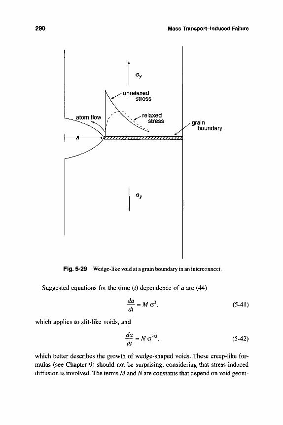
290 Mass Transport-lnduced Failure
' unrelaxed stress
/////////////////////////A
\y gram boundary
Fig. 5-29 Wedge-like void at a grain boundary in an interconnect.
Suggested equations for the time (0 dependence of a are (44)
—— = M c , dt
which applies to slit-like voids, and
da dt
= Na ,3/2
(5-41)
(5-42)
which better describes the growth of wedge-shaped voids. These creep-like for-mulas (see Chapter 9) should not be surprising, considering that stress-induced diffusion is involved. The terms M and A are constants that depend on void geom-
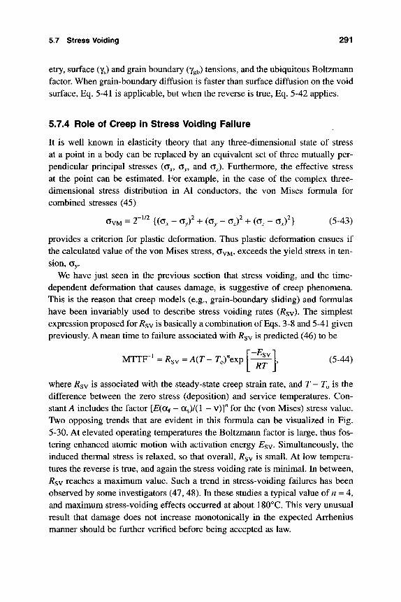
5.7 Stress Voiding 291
etry, surface (YS) and grain boundary (Ygb) tensions, and the ubiquitous Boltzmann factor. When grain-boundary diffusion is faster than surface diffusion on the void surface, Eq. 5-41 is appUcable, but when the reverse is true, Eq. 5-42 appHes.
5.7.4 Role of Creep in Stress Voiding Failure
It is well known in elasticity theory that any three-dimensional state of stress at a point in a body can be replaced by an equivalent set of three mutually per-pendicular principal stresses (GJ,, Cy, and a^). Furthermore, the effective stress at the point can be estimated. For example, in the case of the complex three-dimensional stress distribution in Al conductors, the von Mises formula for combined stresses (45)
GvM = 2"^'' {(CT. - Cyf + (Cy - of + (a, - a,f} (5-43)
provides a criterion for plastic deformation. Thus plastic deformation ensues if the calculated value of the von Mises stress, CYM, exceeds the yield stress in ten-sion, Gy.
We have just seen in the previous section that stress voiding, and the time-dependent deformation that causes damage, is suggestive of creep phenomena. This is the reason that creep models (e.g., grain-boundary sliding) and formulas have been invariably used to describe stress voiding rates (Rsy)- The simplest expression proposed for R^y is basically a combination of Eqs. 3-8 and 5-41 given previously. A mean time to failure associated with /?sv is predicted (46) to be
MTTF^^ - RsY = A{T - T^c^p -sv RT
(5-44)
where Rsy is associated with the steady-state creep strain rate, and T- T^is the difference between the zero stress (deposition) and service temperatures. Con-stant A includes the factor [£(af - as)/(l - v)]" for the (von Mises) stress value. Two opposing trends that are evident in this formula can be visualized in Fig. 5-30. At elevated operating temperatures the Boltzmann factor is large, thus fos-tering enhanced atomic motion with activation energy Esy. Simultaneously, the induced thermal stress is relaxed, so that overall, R^y is small. At low tempera-tures the reverse is true, and again the stress voiding rate is minimal. In between, Rsy reaches a maximum value. Such a trend in stress-voiding failures has been observed by some investigators (47, 48). In these studies a typical value of w = 4, and maximum stress-voiding effects occurred at about 180°C. This very unusual result that damage does not increase monotonically in the expected Arrhenius manner should be further verified before being accepted as law.
292 Mass Transport-Induced Failure
z Q o > CO CO LLi DC H CO U-
o LU
^STRESS- A(T-To)^
/ sv = > (T-To)" exp [-Esv/HT]
CREEP -exp[-Esv/RT]
TEMPERATURE
Fig. 5-30 Stress voiding rate as a function of temperature. The shape of the curve reflects the competition between creep and stress relaxation effects. After reference 46.
5.7.5 Stress Voiding at Vias
Stress voiding is manifested not only along the sides of isolated aluminum inter-connects, it occurs also at vias (49). After the via hole is etched open it is usu-ally annealed to ~450°C to remove impurities that promote corrosion or adversely affect surface migration and nucleation of the subsequently deposited plug metals of Al or W. This creates the reliability problem depicted in Fig. 5-31. Upon heating, the Al expands more than the Si02, compressing the metal over the central portion of the stripe (Lg). At the via hole the stress-free state results in the development of a stress gradient that forces Al atoms to be extruded into the via. This leaves vacancies behind at the LJLc interface, and they condense into voids. The damage has been done, and it is not reversed on cooling. Apparently, the excess high-temperature vacancies now precipitate and further stabilize the voids. In support of this mechanism, experimental studies have revealed greater volumes of extruded metal with increasing distance between vias. Greater void densities are produced during both higher tempera-ture and longer time anneals.
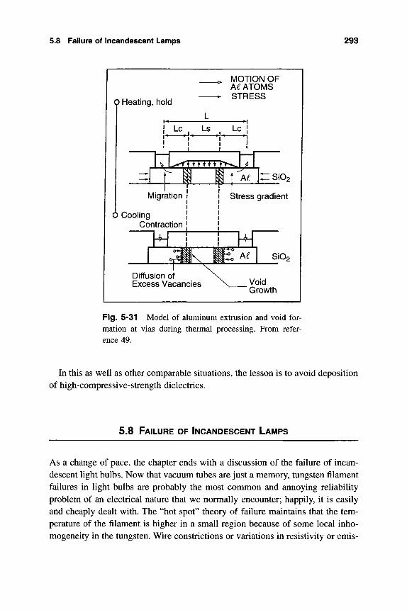
5.8 Failure of Incandescent Lamps 293
9 Heating, hold
MOTION OF A€ ATOMS STRESS
I Lc , j " " i "
L
' - ^ . 1
Lc j
LiXl T: ^™1
Migration
6 Cooling Contraction
A€ :Si02
Stress gradient
SiOo
Diffusion of Excess Vacancies Void
Growth
Fig. 5-31 Model of aluminum extrusion and void for-mation at vias during thermal processing. From refer-ence 49.
In this as well as other comparable situations, the lesson is to avoid deposition of high-compressive-strength dielectrics.
5.8 FAILURE OF INCANDESCENT LAMPS
As a change of pace, the chapter ends with a discussion of the failure of incan-descent light bulbs. Now that vacuum tubes are just a memory, tungsten filament failures in light bulbs are probably the most common and annoying reliability problem of an electrical nature that we normally encounter; happily, it is easily and cheaply dealt with. The "hot spot" theory of failure maintains that the tem-perature of the filament is higher in a small region because of some local inho-mogeneity in the tungsten. Wire constrictions or variations in resistivity or emis-
294 Mass Transport-rnduced Fatture
sivity constitute such inhomogeneities. With time, the temperature difference between the hot spot and the rest of the filament, at temperature T, increases. Preferential evaporation of W not only darkens the inner surface of the bulb, but it thins the filament, making the hot spot hotter, resulting in yet greater evapora-tion. In bootstrap fashion the filament eventually melts or fractures. In this model, applicable to filament metals heated in vacuum, the life of the bulb is exponentially dependent on filament temperature, or correspondingly, inversely proportional to the metal vapor pressure, P. For tungsten, MTTF"* ~ P^ = PQ exp[ - AHy^p/RT], where PQ is a constant, RT has the usual meaning, and A vap» the heat of vaporization, is 183 kcal/mol. Any residual oxygen in the bulb helps to transport W in the form of volatile WO3.
Aside from hot spots, tungsten filaments experience vibration and tend to sag due to elevated temperature creep. The chief operative mechanism for creep damage in lamp filaments is grain-boundary sliding. When this occurs, the fila-ment thins, and the local electrical resistance increases, raising the temperature in the process. Higher temperature accelerates creep deformation (sagging) and leads to yet hotter spots. The cycle feeds on itself, and the filament is well on its way to failure. Making nonsag tungsten wire is a way to attain longer-lasting bulbs. Drawn tungsten wire with minute additions of aluminum and potassium has an interlocking grain-boundary structure that is particularly resistant to slid-ing and creep during high-temperature operation. The grain boundaries make acute angles with respect to the wire axis and are additionally pinned by alloy-ing additions. Nonsag wire is the result.
Common light bulbs are filled with argon. While the main parameter affecting bulb life is the tungsten vapor pressure, Ar alters the gas-phase transport of W. Tungsten atoms no longer fly off in linear paths, but may swirl around in the Ar ambient due to diffusion and convection effects. Bulb dimensions as well as P^ play important roles in influencing MTTF. Filaments are also co^ed. When straight wires are coiled, the effective surface area responsible for mass loss is reduced by a factor of about two. While this may be expected to enhance life proportionately, other W transport mechanisms are operative. A high concentration gradient of tung-sten in the coil promotes gas-phase diffusion, while severe temperature gradients foster surface diffusion along the filament. The latter is responsible for the undesir-able crystallographic faceting of filament grains shown in Fig. 5-32.
Tungsten halogen lamps emit considerably more light than ordinary incandes-cent bulbs because the filament is operated at higher temperatures. The reason they don't fail is due to the chemical-vapor transport of the evaporated W back to the filament. Small amounts of iodine and bromine added to the argon enable the formation of volatile Wl6 and WBr^ compounds, which circulate and regen-erate W upon decomposition.
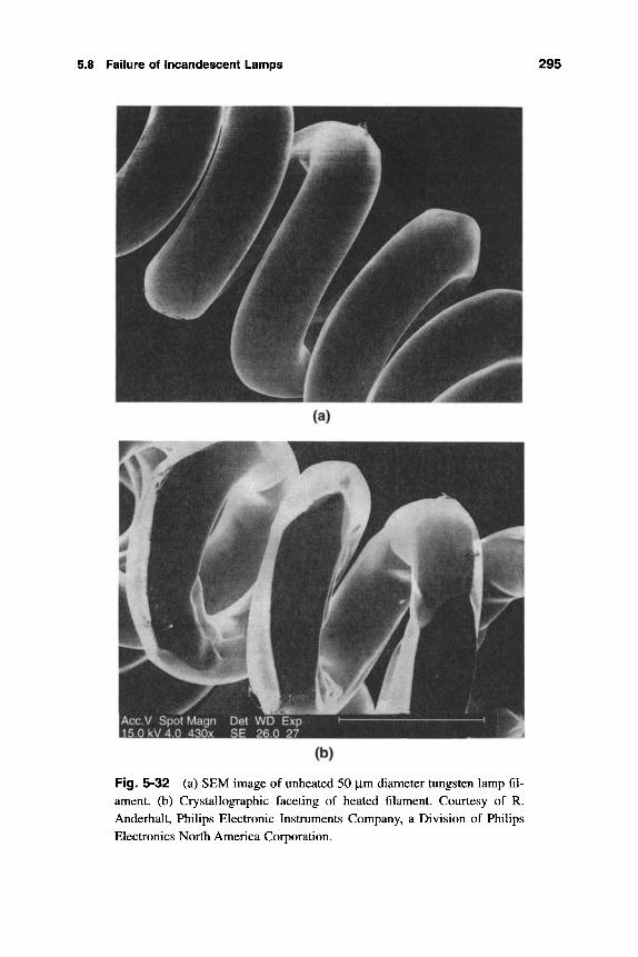
5.8 Failure of Incandescent Lamps 295
Fig. 5-32 (a) SEM image of unheated 50 jim diameter tungsten lamp fil-ament, (b) Crystallographic faceting of heated filament. Courtesy of R. Anderhalt, Philips Electronic Instruments Company, a Division of Philips Electronics North America Corporation.
296 Mass Transport-Induced Failure
EXERCISES
5-1 A finite source layer of A deposited onto the surface of matrix B diffused into it after heating to time ti and the concentration profile versus distance was obtained. a. How would you plot the concentration—distance data to obtain a
straight line? b. If the slope of the line is m, what is the value of the diffusion coefficient? c. What additional information would be required to obtain the activation
energy for diffusion?
5-2 In a couple composed of semi-infinite materials A and B bonded at x = 0, the concentration profile can be curve fit by the equation C (x, t) = ^A Erfc jc/(4Dt)'/2 for oo > jc > -oo. The Matano analysis is designed to extract con-centration-dependent diffusivity values from arbitrary diffusion-couple concentration profiles. Key to the analysis is a graphical integration that is made at any particular value of C (e.g. C) , such that D{C) = - 2i{^)c = c Sf^dC. Using this formula, show that the diffusivity is con-centration-independent for the given profile.
5-3 According to the systematics of diffusion in FCC metals, what are the acti-vation energies for bulk and grain-boundary diffusion in Al, Au, and Cu thin films?
5-4 In considering the reliability of a thin-film Cu-Ni bilayer contact structure for solar cells, it was feared that these metals would interdiffuse and degrade electrical resistance. To estimate contact lifetimes, the available high-temperature lattice-diffusion data for Cu in Ni yielded a D value of 3 X lO" '* cm^/s when extrapolated to 300°C. a. Using this value, how long will it take for these metals to interdiffuse
through 200 nm at 300°C? b. Experiment showed that interdiffusion occurred in an hour. What hap-
pened?
5-5 To prevent silicon and aluminum films from reacting, a diffusion barrier is imposed. What properties are required for optimal function of this barrier?
5-6 Gold bonding wire 25 |xm in diameter is attached to an aluminum film pad 2 \\m thick. a. How long would it take a 0.1 |im thick AuAl2 compound layer to form
if the contact is exposed to a 120°C environment?
Exercises 297
b. Suppose the length of the Au wire is 1000 |Lim, the Al pad has a diame-ter of 25 |im, and the electrical resistivity of AuAl2 is 10 times that for Au. Write an equation for the time-dependence of overall resistance change measured between the metal ends.
5-7 In MESFETs the saturation drain-source current is given by /DSS = QN Vsat ^ ^y where Vsat is the saturation value of electron drift velocity and Z is the gate width. Predict how /QSS will change with time if gate sinking occurs.
5-8 Suppose good pure Al contacts to Si could be produced at low tempera-tures instead of 450°C. Would spiking of junctions 50 nm deep become a reliability problem if such devices operate at 50°C? Make any assumptions you wish.
5-9 Derive the result indicated in Eq. 5-24.
5-10 Consider the steady-state heat flow in a metal stripe where heat loss to the ambient temperature T^ occurs by convection. If the equation describing the temperature {T) at any position (x) is written as
where h is the (constant) heat transfer coefficient, obtain a solution for T{x) using the same boundary conditions as in Sect. 5.5.3.
5-11 Under simultaneous electromigration and diffusional transport show that ^ = D^ - v^, where v is given by DZ^qp jJ^T. Prove by direct substitu-tion that
C(jc, 0 = - ^ exp — Erfc - ^ + Erfc ^ T^
is a solution.
5-12. a. It has been determined that the mean life of pure aluminum stripes of width w (in cm) and thickness d (in cm) is given by MTTF (h) = 4.4 x 10^^ w J7""exp [EJkT], where n = 2,E^ = 0.49 eV, and; is in A /cm^. Which has a greater influence in changing the value of MTTF at 50°C, a 1% change in n or a 1% change in E^l
b. What is the mean life of an interconnect 0.4 |im wide and 0.5 |im thick powered with 1 x 10^ A/cm^? How does it compare to the mean life of an Al-Si interconnect of the same dimensions for which MTTF (h) = 2.2 X 10^^ w dj-^ exp [0.54cY/kW
298 Mass Transport-Induced Failure
5-13 A 0.5 |xm thick aluminum stripe is powered with 1x10^ A/cm^. Assuming typical constants for Al, whose surface energy is 10""* J/cm^, predict how long it would take a grain-boundary groove-hole to reach the substrate.
5-14 Electromigration failure data for pure Al and Al-4wt.% Cu-1.7 wt.%Si interconnects obey lognormal statistics. For pure Al, 50 = 85 h and a = 0.32, while for alloyed Al, tso = 5600 h and a = 0.22. Sketch the behavior of both metallizations to scale on lognormal plots.
5-15 Show that after substitution of the Weibull cumulative distribution function F(t), FN(0 , defined in Eq. 5-33, is also a Weibull distribution.
5-16 A third-level IC interconnect consists of a distribution of Al-Cu stripes deposited over Si02 as well as over the sides and bottoms of via contacts. On the Si02 the stripe width (w) and thickness (d) dimensions are each 5 x 10"^ cm, but in the via w is thinned to 0.25 x 10"^ cm. The conducting length of the stripe is three times that of the via, and the mean life of the interconnect metalHzation is given by MTTF (h) = 2.4 x 10^ w dj~^ exp [0.65cW/kT]. a. What is the ratio of MTTF for the involved interconnect relative to a
Hnear (unthinned) stripe of the same length if 7 = 4 x 10^ A/cm^? b. For an overall conducting length of 1 mm, what is the voltage drop
across the interconnect?
5-17 From the plots of Fig. 5-25 evaluate the constants B, E^, and n in the Black equation (Eq. 5-31).
5-18 Solve the boundary value problem da ^ DBil d^d dt ~ RT dx^
under the following initial and boundary conditions:
At r = 0, jc>0; a = 0.
At X = 0, t ; da/dx = -Z'^qpj^/Q.
At X = 00, t ; a = 0.
Derive an expression for a (x, t).
5-19 Suppose it is desired to passivate aluminum metallization with surrounding layers of Si02, phosphosilicate (PSG), and borophosphosilicate (BPSG) glass, as well as silicon nitrides. In each case the insulators are deposited at ~ 400''C and cooled to 25°C, a process that thermally stresses the Al.
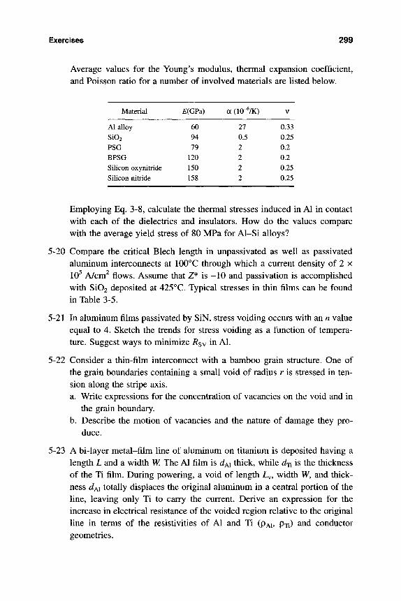
Exercises 299
Average values for the Young's modulus, thermal expansion coefficient, and Poisson ratio for a number of involved materials are listed below.
Material
Al alloy
Si02 PSG BPSG Silicon oxynitride Silicon nitride
£:(GPa)
60 94 79
120 150 158
a (10-^/K)
27 0.5 2 2 2 2
V
0.33 0.25 0.2 0.2 0.25 0.25
Employing Eq. 3-8, calculate the thermal stresses induced in Al in contact with each of the dielectrics and insulators. How do the values compare with the average yield stress of 80 MPa for Al-Si alloys?
5-20 Compare the critical Blech length in unpassivated as well as passivated aluminum interconnects at 100°C through which a current density of 2 x 10^ A/cm^ flows. Assume that Z* is -10 and passivation is accomplished with Si02 deposited at 425°C. Typical stresses in thin films can be found in Table 3-5.
5-21 In aluminum films passivated by SiN, stress voiding occurs with an n value equal to 4. Sketch the trends for stress voiding as a function of tempera-ture. Suggest ways to minimize R^y in Al.
5-22 Consider a thin-film interconnect with a bamboo grain structure. One of the grain boundaries containing a small void of radius r is stressed in ten-sion along the stripe axis. a. Write expressions for the concentration of vacancies on the void and in
the grain boundary. b. Describe the motion of vacancies and the nature of damage they pro-
duce.
5-23 A bi-layer metal-film line of aluminum on titanium is deposited having a length L and a width W. The Al film is JAI thick, while Jji is the thickness of the Ti film. During powering, a void of length L , width W, and thick-ness JAI totally displaces the original aluminum in a central portion of the line, leaving only Ti to carry the current. Derive an expression for the increase in electrical resistance of the voided region relative to the original line in terms of the resistivities of Al and Ti (pAi, pxi) and conductor geometries.
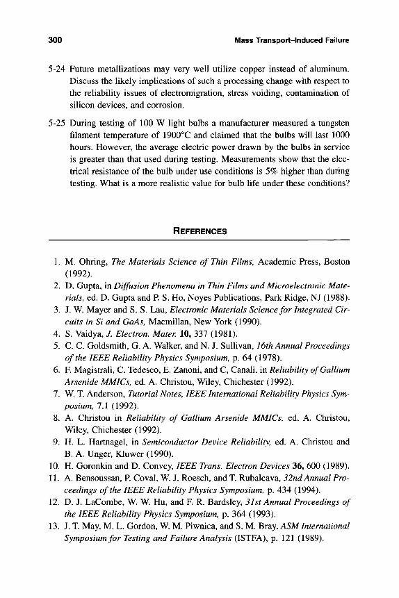
300 Mass Transport-Induced Failure
5-24 Future metallizations may very well utilize copper instead of aluminum. Discuss the likely implications of such a processing change with respect to the reliability issues of electromigration, stress voiding, contamination of silicon devices, and corrosion.
5-25 During testing of 100 W light bulbs a manufacturer measured a tungsten filament temperature of 1900°C and claimed that the bulbs will last 1000 hours. However, the average electric power drawn by the bulbs in service is greater than that used during testing. Measurements show that the elec-trical resistance of the bulb under use conditions is 5% higher than during testing. What is a more realistic value for bulb life under these conditions?
REFERENCES
1. M. Ohring, The Materials Science of Thin Films, Academic Press, Boston (1992).
2. D. Gupta, in Diffusion Phenomena in Thin Films and Microelectronic Mate-rials, ed. D. Gupta and P. S. Ho, Noyes Publications, Park Ridge, NJ (1988).
3. J. W. Mayer and S. S. Lau, Electronic Materials Science for Integrated Cir-cuits in Si and GaAs, Macmillan, New York (1990).
4. S. Vaidya, J. Electron. Mater 10, 337 (1981). 5. C. C. Goldsmith, G. A. Walker, and N. J. Sullivan, 16th Annual Proceedings
of the IEEE Reliability Physics Symposium, p. 64 (1978). 6. F. Magistrali, C. Tedesco, E. Zanoni, and C, Canali, in Reliability of Gallium
Arsenide MMICs, ed. A. Christou, Wiley, Chichester (1992). 7. W. T. Anderson, Tutorial Notes, IEEE International Reliability Physics Sym-
posium, 7.1 (1992). 8. A. Christou in Reliability of Gallium Arsenide MMICs, ed. A. Christou,
Wiley, Chichester (1992). 9. H. L. Hartnagel, in Semiconductor Device Reliability, ed. A. Christou and
B. A. Unger, Kluwer (1990). 10. H. Goronkin and D. Convey, IEEE Trans. Electron Devices 36, 600 (1989). 11. A. Bensoussan, P. Coval, W. J. Roesch, and T. Rubalcava, 32nd Annual Pro-
ceedings of the IEEE Reliability Physics Symposium, p. 434 (1994). 12. D. J. LaCombe, W. W. Hu, and F. R. Bardsley, 31st Annual Proceedings of
the IEEE Reliability Physics Symposium, p. 364 (1993). 13. J. T. May, M. L. Gordon, W. M. Piwnica, and S. M. Bray, ASM International
Symposium for Testing and Failure Analysis (ISTFA), p. 121 (1989).
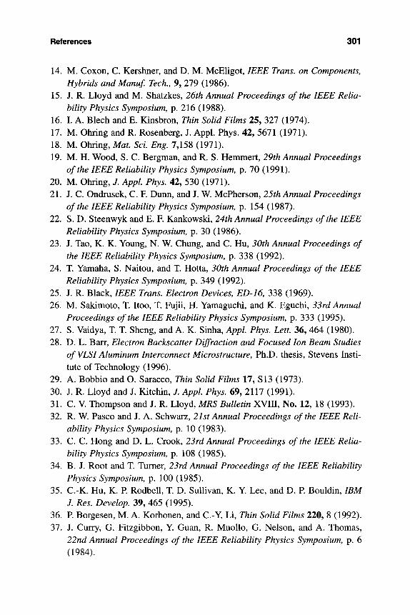
References 301
14. M. Coxon, C. Kershner, and D. M. McEligot, IEEE Trans, on Components, Hybrids and Manuf. Tech., 9, 279 (1986).
15. J. R. Lloyd and M. Shatzkes, 26th Annual Proceedings of the IEEE Relia-bility Physics Symposium, p. 216 (1988).
16. I. A. Blech and E. Kinsbron, Thin Solid Films 25, 327 (1974). 17. M. Ohring and R. Rosenberg, J. Appl. Phys. 42, 5671 (1971). 18. M. Ohring, Mat. Sci. Eng. 7,158 (1971). 19. M. H. Wood, S. C. Bergman, and R. S. Hemmert, 29th Annual Proceedings
of the IEEE Reliability Physics Symposium, p. 70 (1991). 20. M. Ohring, J. Appl. Phys. 42, 530 (1971). 21. J. C. Ondrusek, C. F. Dunn, and J. W. McPherson, 25th Annual Proceedings
of the IEEE Reliability Physics Symposium, p. 154 (1987). 22. S. D. Steenwyk and E. F. Kankowski, 24th Annual Proceedings of the IEEE
Reliability Physics Symposium, p. 30 (1986). 23. J. Tao, K. K. Young, N. W. Chung, and C. Hu, 30th Annual Proceedings of
the IEEE Reliability Physics Symposium, p. 338 (1992). 24. T. Yamaha, S. Naitou, and T. Hotta, 30th Annual Proceedings of the IEEE
Reliability Physics Symposium, p. 349 (1992). 25. J. R. Black, IEEE Trans. Electron Devices, ED-16, 338 (1969). 26. M. Sakimoto, T. Itoo, T. Fujii, H. Yamaguchi, and K. Eguchi, 33rd Annual
Proceedings of the IEEE Reliability Physics Symposium, p. 333 (1995). 27. S. Vaidya, T. T. Sheng, and A. K. Sinha, Appl. Phys. Lett. 36, 464 (1980). 28. D. L. Barr, Electron Backscatter Diffraction and Focused Ion Beam Studies
of VLSI Aluminum Interconnect Microstructure, Ph.D. thesis, Stevens Insti-tute of Technology (1996).
29. A. Bobbio and O. Saracco, Thin Solid Films 17, S13 (1973). 30. J. R. Lloyd and J. Kitchin, /. Appl. Phys. 69, 2117 (1991). 31. C. V. Thompson and J. R. Lloyd, MRS Bulletin XVIII, No. 12, 18 (1993). 32. R. W. Pasco and J. A. Schwarz, 21 st Annual Proceedings of the IEEE Reli-
ability Physics Symposium, p. 10 (1983). 33. C. C. Hong and D. L. Crook, 23rd Annual Proceedings of the IEEE Relia-
bility Physics Symposium, p. 108 (1985). 34. B. J. Root and T. Turner, 23rd Annual Proceedings of the IEEE Reliability
Physics Symposium, p. 100 (1985). 35. C.-K. Hu, K. R Rodbell, T. D. Sullivan, K. Y. Lee, and D. P Bouldin, IBM
J. Res. Develop. 39, 465 (1995). 36. P Borgesen, M. A. Korhonen, and C.-Y. Li, Thin Solid Films 220, 8 (1992). 37. J. Curry, G. Fitzgibbon, Y Guan, R. MuoUo, G. Nelson, and A. Thomas,
22nd Annual Proceedings of the IEEE Reliability Physics Symposium, p. 6 (1984).
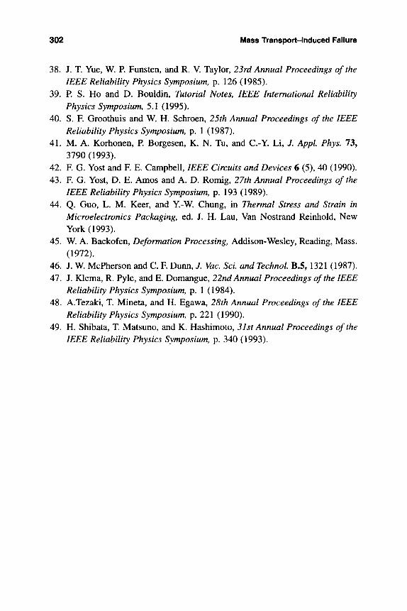
302 Mass Transport-Induced Failure
38. J. T. Yue, W. P. Funsten, and R. V. Taylor, 23rd Annual Proceedings of the IEEE Reliability Physics Symposium, p. 126 (1985).
39. P. S. Ho and D. Bouldin, Tutorial Notes, IEEE International Reliability Physics Symposium, 5.1 (1995).
40. S. F. Groothuis and W. H. Schroen, 25th Annual Proceedings of the IEEE Reliability Physics Symposium, p. 1 (1987).
41. M. A. Korhonen, P Borgesen, K. N. Tu, and C.-Y. Li, J. Appl Phys. 73, 3790 (1993).
42. F. G. Yost and F. E. Campbell, IEEE Circuits and Devices 6 (5), 40 (1990). 43. F. G. Yost, D. E. Amos and A. D. Romig, 27th Annual Proceedings of the
IEEE Reliability Physics Symposium, p. 193 (1989). 44. Q. Guo, L. M. Keer, and Y-W. Chung, in Thermal Stress and Strain in
Microelectronics Packaging, ed. J. H. Lau, Van Nostrand Reinhold, New York (1993).
45. W. A. Backofen, Deformation Processing, Addison-Wesley, Reading, Mass. (1972).
46. J. W. McPherson and C. F. Dunn, J. Vac. ScL and Technol B.5,1321 (1987). 47. J. Klema, R. Pyle, and E. Domangue, 22nd Annual Proceedings of the IEEE
Reliability Physics Symposium, p. 1 (1984). 48. A.Tezaki, T. Mineta, and H. Egawa, 28th Annual Proceedings of the IEEE
Reliability Physics Symposium, p. 221 (1990). 49. H. Shibata, T. Matsuno, and K. Hashimoto, 31st Annual Proceedings of the
IEEE Reliability Physics Symposium, p. 340 (1993).
Chapter 6
Electronic Charge-Induced Damage
6-1 INTRODUCTION
To the extent that the degradation and failure effects are the consequence of mat-ter transport, this time of electrons and holes, we may view this chapter as a companion to the previous one. Whereas metal-metal, metal-semiconductor, and electron-metal interactions were largely the focus of Chapter 5, here our interest is primarily in insulators and the corresponding electron (hole)-electron or electron-atom interactions. The physical laws that govern the motion of neu-tral atoms and electronic carriers differ, and the damage wreaked by their motion also differs markedly. Insulators, and to a lesser extent semiconductors, rather than conductors, are the primary victims of electric field-induced accumulation and transport of electronic charge. Nonsemiconductor electrical components, such as transformer oil and high-voltage ceramic and polymer insulation, are also susceptible to electron charging and discharging damage.
The phenomena of dielectric breakdown, hot electron transport, and electro-static discharge, all serious reliability issues in integrated circuit devices, are the primary focus of this chapter. Central to an understanding these specific charge-induced damage phenomena are the electrical conduction mechanisms in insula-tors (1). In all cases damage is directly proportional to the amount of accumu-lated charge and the way it is subsequently redistributed. We start by considering
303
304 Electronic Charge-Induced Damage
the nature of charge transport in insulators, materials we don't normally think of as being able to conduct electricity.
6.2 ASPECTS OF CONDUCTION IN INSULATORS
6.2.1 Current-Voltage Relationships
When sufficiently high electric fields, (^(V/cm), are applied to insulators, the response is passage of a current of density j (A/cm^). If ^ is small, the response is generally linear or ohmic, and the conductivity (a), given by j/S', is indepen-dent of S'. For larger applied fields the j-S' relationships defining charge trans-port through insulators are more complex. Depending on mechanism, the con-duction characteristics are described by one or more of the equations listed in Table 6-1. In most cases the magnitude of 7 is strongly temperature-dependent according to the usual Maxwell-Boltzmann factor.
Charge injection into insulators from either metal or semiconductor contacts is usually modeled in terms of band diagrams. The case of electron injection from the gate electrode into the oxide of an MOS structure is schematically indi-cated in Fig. 6-1. Even modest voltages (V) can generate extremely high electric fields across thin oxides of thickness (do) because co = dV/dx or V/d^. The elec-tric field supported by the insulator is represented by the sloped potential curve; steeper slopes mean higher <o fields. Where local fields are highest, electrons from the gate enter the insulator conduction band by either 1. climbing over the electron energy barrier (Fig. 6-la) or by 2. burrowing or tunneling through the triangular barrier shown in Fig. 6-lb. The first of these processes, known as Schottky emission, resembles thermionic emission and typically has the T^ exp [-^^/kT] dependence, where OB is the barrier height. However, the appUed elec-tric field causes a continuously varying electron potential-energy variation at the interface rather than an abrupt change. When an electron enters the insulator, it produces a so-called image field that adds to the barrier field, effectively lower-ing it. The result is a reduced barrier height and an enhanced current given by the second exponential factor in Eq. 6-1. Overall, the j-S" characteristics reveal that current injection depends strongly on the barrier height, temperature, and electric field.
The electron-tunneling mechanism is quantum-mechanical in origin and depends on there being empty states in the insulator available for electrons to occupy. Resulting currents depend very strongly on S', but unlike other conduc-tion mechanisms, tunneling characteristics (Eq. 6-3) are temperature-indepen-
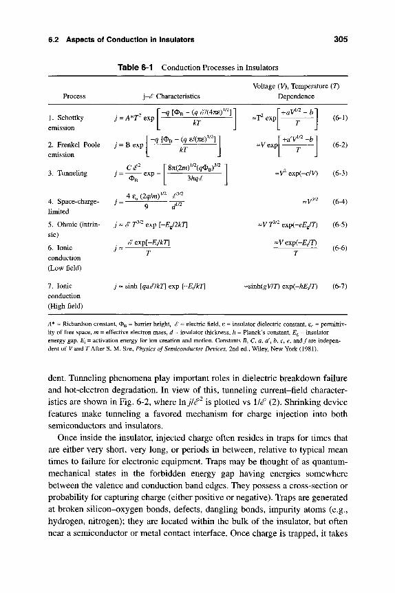
6.2 Aspects of Conduction in Insulators 305
Table 6-1 Conduction Processes in Insulators
Process ' Characteristics Voltage (V), Temperature (T)
Dependence
1. Schottky emission
3. Tunneling
4. Space-charge-limited
5. Ohmic (intrin-sic)
6. Ionic conduction (Low field)
7. Ionic conduction (High field)
j = A*T exp -q[^^-iq^/(4TtEf^]
2. Frenkel-Poole 7 = B exp emission
kT
•q [OB - {q d{nzf'^]
Op - exp -
kT
m2m)"\q(^^f'^
4 8„ {Iqimf
j^S T'^ exp \-EJlkT\
S Qyj^\-EJkT\ J - ^
j - sinh [q2iSlkT\ exp [-E^lkT]
=T^ exp
=V exp
\aV"^-b T
(6-1)
(6-2)
-V^ exp(-c/V) (6-3)
-y^^^ (6-4)
=y r'^^ QX^{-eEJT) (6-5)
==^Vexp(-£,/D (6-6)
-sinh(gV/r) expi-hE^/T) (6-7)
A* = Richardson constant, OB = barrier height, / = electric field, e = insulator dielectric constant, £o = permittiv-ity of free space, m = effective electron mass, d = insulator thickness, h = Planck's constant. Eg = insulator energy gap, E^ = activation energy for ion creation and motion. Constants B, C, a, a, b, c, e, and/are indepen-dent of y and r After S. M. Sze, Physics of Semiconductor Devices, 2nd ed., Wiley, New York (1981).
dent. Tunneling phenomena play important roles in dielectric breakdown failure and hot-electron degradation. In view of this, tunneling current-field character-istics are shown in Fig. 6-2, where Xnjli^ is plotted vs \IS (2). Shrinking device features make tunneling a favored mechanism for charge injection into both semiconductors and insulators.
Once inside the insulator, injected charge often resides in traps for times that are either very short, very long, or periods in between, relative to typical mean times to failure for electronic equipment. Traps may be thought of as quantum-mechanical states in the forbidden energy gap having energies somewhere between the valence and conduction band edges. They possess a cross-section or probability for capturing charge (either positive or negative). Traps are generated at broken silicon-oxygen bonds, defects, dangling bonds, impurity atoms (e.g., hydrogen, nitrogen); they are located within the bulk of the insulator, but often near a semiconductor or metal contact interface. Once charge is trapped, it takes
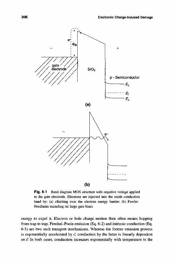
306 Electronic Charge-Induced Damage
p - Semiconductor
• ^ c
-f
(a)
Fig. 6-1 Band diagram MOS structure with negative voltage applied to the gate electrode. Electrons are injected into the oxide conduction band by: (a) climbing over the electron energy barrier, (b) Fowler-Nordheim tunneling (at large gate bias).
energy to expel it. Electron or hole charge motion then often means hopping from trap to trap. Frenkel-Poole emission (Eq. 6-2) and intrinsic conduction (Eq. 6-5) are two such transport mechanisms. Whereas the former emission process is exponentially accelerated by S, conduction by the latter is linearly dependent on S. In both cases, conduction increases exponentially with temperature in the
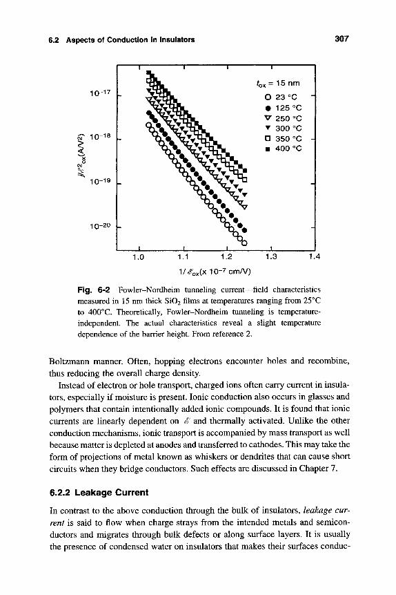
6.2 Aspects of Conduction in Insuiators 307
10-17 I
i T 10-18 L
10-19 L
10-20
1.0 1.1 1.2
1/#ox(x lO-^Gin/V)
1.4
Fig. 6-2 Fowler-Nordheim tunneling current—field characteristics measured in 15 nm thick Si02 films at temperatures ranging from 25°C to 400°C. Theoretically, Fowler-Nordheim tunneling is temperature-independent. The actual characteristics reveal a slight temperature dependence of the barrier height. From reference 2.
Boltzmann manner. Often, hopping electrons encounter holes and recombine, thus reducing the overall charge density.
Instead of electron or hole transport, charged ions often carry current in insula-tors, especially if moisture is present. Ionic conduction also occurs in glasses and polymers that contain intentionally added ionic compounds. It is found that ionic currents are linearly dependent on S and thermally activated. Unlike the other conduction mechanisms, ionic transport is accompanied by mass transport as well because matter is depleted at anodes and transferred to cathodes. This may take the form of projections of metal known as whiskers or dendrites that can cause short circuits when they bridge conductors. Such effects are discussed in Chapter 7.
6.2.2 Leakage Current
In contrast to the above conduction through the bulk of insulators, leakage cur-rent is said to flow when charge strays from the intended metals and semicon-ductors and migrates through bulk defects or along surface layers. It is usually the presence of condensed water on insulators that makes their surfaces conduc-
308 Electronic Charge-Induced Damage
tive. As a result of such surface ion effects, corrosion, electrical arcing, and par-tial short-circuiting, overall circuit characteristics often degrade progressively over a long time, but sometimes with catastrophic abruptness. The surface cur-rent is ohmic and generally expressed by a formula of the type
j = AS' QxpibxRH) expj ^ j , (6-8)
where RH is the relative humidity, E is the activation energy for conduction, and A and b are constants. Values of E for a number of insulators range from 0.4 to 1.1 eV, while b is approximately 0.1 to 0.3 (3). An analysis shows that b depends on the extent of water-vapor adsorption and is thus strongly temperature-dependent.
6.2.3 Si02—Electrons, Holes, Ions, and Traps
Silicon technology owes much to the remarkable properties of Si02 in its crucial function as the gate oxide, for fulfilling passivating, insulating and dielectric needs, and for its important role in masking and processing. However, the demands made on the gate oxide simultaneously make it the target of several important degradation effects in MOS transistors. Thus, dielectric breakdown, hot electron transport (4), radiation damage, and some modes of electrostatic dis-charge failure are phenomena intimately associated with charge transport in thin Si02 films. Although the microscopic details are controversial and sometimes confusing (5), the picture of the four different kinds of charge associated with the unbiased Si-Si02 system and their location within it, is shown in Fig. 6-3.
1. Mobile Na" and K" ionic charge, may be present in Si02. Introduced as con-tamination during processing, this source of oxide charge has been virtually eliminated as a source of reliability problems.
2. Secondly, there is the oxide trapped charge, which is distributed throughout the bulk of the Si02 film. A portion of this charge (Qb) stems from process-ing and can be removed through low-temperature annealing. X-ray radiation and high-energy electrons are additional sources of Qb- Oxide-trapped charge is associated with shallow traps that are not located near the Si-Si02 inter-face. Electron and hole traps apparently contain Si dangling bonds (Si-0)3 = Si* and oxygen dangling bonds (Si-0)3 = S i - 0 - to which charge attaches. (The symbol "-" denotes an electron-pair bond, while "*" signifies an unpaired or dangling electron bond.)
3. Next we consider the positive fixed oxide charge density (gf), which is located some 3 to 5 nm from the Si-Si02 interface. Because such charge is fixed, it does not usually charge or discharge and is largely uninfluenced by the normal operating voltages of the MOS transistor. Regarded as a sheet of
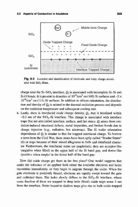
6.2 Aspects of Conduction in insulators 309
SiOp
SJO^
Si (substrate)
© © •
Oxide Trapped Ciiarge
^Nv + + + +
+ + + + +
fi Ji fi
^ Mobile Ionic Charge
Fixed Oxide Charge
+ + + + w I f w w 1
H H if H 1
\ Interface Trapped Charge
Fig. 6-3 Location and identification of electronic and ionic charge associ-ated with Si02 films.
charge near the Si-Si02 interface, Qf is associated with incomplete Si-Si and Si-O bonds. It is present in densities of lO^^m^ on (100) Si surfaces and ~5 x 10^ /cm^ on (111) Si surfaces. In addition to silicon orientation, the distribu-tion and density of Qf is related to the thermal oxidation process and depends on the oxidation temperature and subsequent cooling rate.
4. Lastly, there is interfacial oxide charge density, Qi, that is localized within -0.2 nm of the Si02-Si interface. This charge is associated with interface traps that are also called interface, surface, and fast states. Qi arises from oxi-dation-induced structural defects, metal impurities, and broken bonds due to charge injection (e.g., radiation, hot electrons). The Si wafer orientation dependence of Q^ is similar to that for trapped interfacial charge. To borrow a term from the Civil War, these states have been aptly called "Border States" (6) or traps because of their mixed allegiance to bulk and interfacial charac-ter. Furthermore, the interfacial states are amphoteric; they are acceptor-like (negative when filled) in the upper half of the Si band gap, and donor-like (positive when empty) in the lower half of the band gap.
How did oxide charge get there in the first place? One model suggests that under the influence of an applied field either the available electrons and holes recombine immediately, or they begin to migrate through the oxide. When the gate electrode is positively biased, electrons are rapidly swept toward the gate and collected there. The holes slowly diffuse to the Si02-Si interface, where some fraction of them are trapped in deep hole (fixed) oxide traps some 5 nm from the interface. Holes bound to shallow traps give rise to bulk oxide-trapped
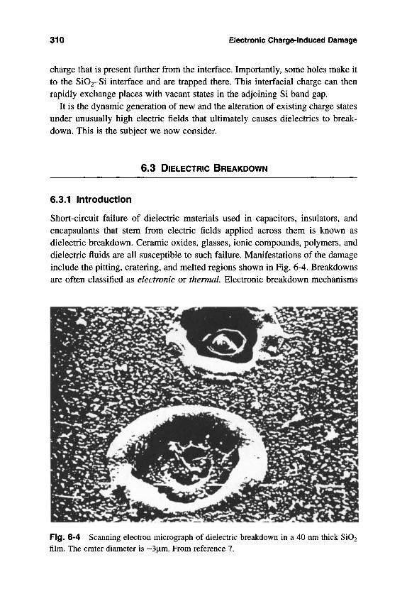
310 Electronic Charge-Induced Damage
charge that is present further from the interface. Importantly, some holes make it to the Si02-Si interface and are trapped there. This interfacial charge can then rapidly exchange places with vacant states in the adjoining Si band gap.
It is the dynamic generation of new and the alteration of existing charge states under unusually high electric fields that ultimately causes dielectrics to break-down. This is the subject we now consider.
6.3 DIELECTRIC BREAKDOWN
6.3.1 Introduction
Short-circuit failure of dielectric materials used in capacitors, insulators, and encapsulants that stem from electric fields applied across them is known as dielectric breakdown. Ceramic oxides, glasses, ionic compounds, polymers, and dielectric fluids are all susceptible to such failure. Manifestations of the damage include the pitting, cratering, and melted regions shown in Fig. 6-4. Breakdowns are often classified as electronic or thermal. Electronic breakdown mechanisms
Fig. 6-4 Scanning electron micrograph of dielectric breakdown in a 40 nm thick Si02 film. The crater diameter is ~3|im. From reference 7.
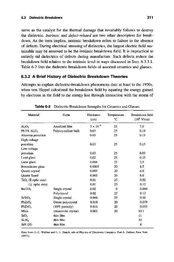
6.3 Dielectric Brealcdown 311
serve as the catalyst for the thermal damage that invariably follows to destroy the dielectric. Intrinsic and defect-related are two other descriptors for break-down. As the term implies, intrinsic breakdown refers to failure in the absence of defects. During electrical stressing of dielectrics, the largest electric field sus-tainable may be assumed to be the intrinsic breakdown field. It is impractical to entirely rid dielectrics of defects during manufacture. Such defects reduce the breakdown field relative to the intrinsic level in ways discussed in Sect. 6.3.3.1. Table 6-2 lists the dielectric breakdown fields of assorted ceramics and glasses.
6.3.2 A Brief History of Dielectric Breakdown Theories
Attempts to explain dielectric-breakdown phenomena date at least to the 1930s, when von Hippel calculated the breakdown field by equating the energy gained by electrons in the field to the energy lost through interaction with the atoms of
Table 6-2
Material
AI2O3 99.5% AI2O3 Alumina porcelain High-voltage porcelain Low-voltage porcelain Lead glass Lime glass Borosilicate glass Quartz crystal Quartz fused Ti02 (II optic axis)
(J. optic axis) BaTiOs
SrTiOg PbZrOg
PbZrOg Mica
Si02 Si3N4 SiN (H)
Dielectric Breakdown Strengths
Form
Anodized film Polycrystalline bulk
Single crystal Poly crystal Single crystal Dense polycrystal (10% porosity) (muscovite crystal) thin film thin film thin film
Thickness (cm)
3 X 10"^ 0.63 0.63
0.63
a63 0.02 0.004 0.0005 0.005 0.005 0.01 0.01 0.02 0.02 0.046 0.016 0.016 0.002
for Ceramics and Glasses
Temperature °C
25 25 25
25
25 25 25 20 20 20 25 25 0
25 25 20 20 20
Breakdown field (10^ V/cm)
7.0 0.18 0.15
0.15
0.03 0.25 2.5 6.5 6.0 6.6 0.02 0.12 0.040 0.12 0.41 0.079 0.033
10.1 11 10 6
Data from G. C. Walther and L. L. Hench, eds of Physics of Electronic Ceramics, Part A, Dekker, New York (1971).
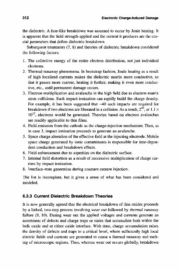
312 Electronic Charge-Induced Damage
the dielectric. A fuse-like breakdown was assumed to occur by Joule heating. It is apparent that the field strength applied and the current it produces are the cru-cial parameters that define dielectric breakdown.
Subsequent treatments (7, 8) and theories of dielectric breakdown considered the following factors:
1. The collective energy of the entire electron distribution, not just individual electrons.
2. Thermal-runaway phenomena. In bootstrap fashion, Joule heating as a result of high localized currents makes the dielectric matrix more conductive, so that it passes more current, heating it further, making it even more conduc-tive, etc., until permanent damage occurs.
3. Electron multiplication and avalanche in the high field due to electron-matrix atom collisions. Such impact ionization can rapidly build the charge density. For example, it has been suggested that ~40 such impacts are required for breakdown if two electrons are liberated in a collision. As a result, 2^^, or 1.1 x 10^ , electrons would be generated. Theories based on electron avalanches are readily applicable to thin films.
4. Field emission from the cathode as the charge-injection mechanism. Then, as in case 3, impact ionization proceeds to generate an avalanche.
5. Space charge alteration of the effective field at the injecting electrode. Mobile space charge generated by ionic contaminants is responsible for time-depen-dent conduction and breakdown effects.
6. Field enhancement due to asperities on the dielectric surface. 7. Internal field distortion as a result of successive multiplication of charge car-
riers by impact ionization. 8. Interface-state generation during constant current injection.
The list is incomplete, but it gives a sense of what has been considered and modeled.
6.3.3 Current Dielectric Brealcdown Theories
It is now generally agreed that the electrical breakdown of thin oxides proceeds by a linked, two-step process involving wear out followed by thermal runaway failure (9, 10). During wear out the applied voltages and currents generate an assortment of defects and charge traps or states that accumulate both within the bulk oxide and at either oxide interface. With time, charge accumulation raises the density of defects and traps to a critical level, where sufficiently high local electric fields and currents are generated to cause a thermal runaway and melt-ing of microscopic regions. Thus, whereas wear out occurs globally, breakdown
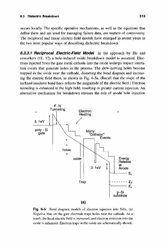
6.3 Dielectric Breakdown 313
occurs locally. The specific operative mechanisms, as well as the equations that define them and are used for managing failure data, are matters of controversy. The reciprocal and linear electric-field models have emerged in recent years as the two most popular ways of describing dielectric breakdown.
6.3.3.1 Reciprocal Electric-Field Model In the approach by Hu and coworkers (11, 12) a hole-induced oxide breakdown model is assumed. Elec-trons injected from the gate metal cathode into the oxide undergo impact ioniza-tion events that generate holes in the process. The slow-moving holes become trapped in the oxide near the cathode, distorting the band diagram and increas-ing the electric field there, as shown in Fig. 6-5a. (Recall that the slope of the inclined insulator band lines reflects the magnitude of the electric field.) Electron tunneUng is enhanced in the high field, resulting in greater current injection. An alternative mechanism for breakdown stresses the role of anode hole injection
F-N Tunneling
3. 1eV
Electron Heating
poly - Si gate Many
"Collision" Events
Energy Release at Anode
p-Si substrate
Fig. 6-5 Band diagram models of electron injection into Si02. (a) Negative bias on the gate electrode traps holes near the cathode. As a result, the local electric field is increased, and electron emission into the oxide is enhanced. Electron traps in the oxide are schematically shown.
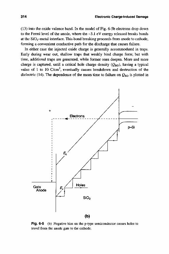
314 Electronic Charge-Induced Damage
(13) into the oxide valence band. In the model of Fig. 6-5b electrons drop down to the Fermi level of the anode, where the -3.1 eV energy released breaks bonds at the Si02-metal interface. This bond breaking proceeds from anode to cathode, forming a convenient conductive path for the discharge that causes failure.
In either case the injected oxide charge is generally accommodated in traps. Early during wear out, shallow traps that weakly bind charge form; but with time, additional traps are generated, while former ones deepen. More and more charge is captured, until a critical hole charge density (QBD)» having a typical value of 1 to 10 C/cm^, eventually causes breakdown and destruction of the dielectric (14). The dependence of the mean time to failure on QBD is plotted in
(b)
Fig. 6-5 (b) Negative bias on the p-type semiconductor causes holes to travel from the anode gate to the cathode.
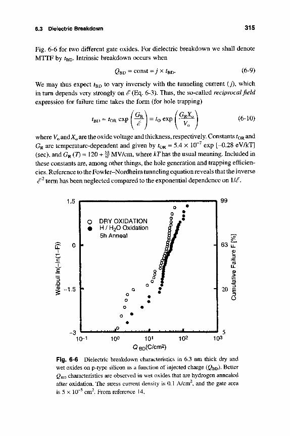
e.3 Dielectric Breakdown 315
Fig. 6-6 for two different gate oxides. For dielectric breakdown we shall denote MTTF by ^BD- Intrinsic breakdown occurs when
(3BD = const==:7X%p. (6-9)
We may thus expect %D to vary inversely with the tunneling current (;), which in turn depends very strongly on i (Eq. 6-3). Thus, the so-called reciprocal field expression for failure time takes the form (for hole trapping)
%D - OR ^XP (t) = 'o exp (6-10)
where VQ and JQ are the oxide voltage and thickness, respectively. Constants ^QR and GR are temperature-dependent and given by ^QR = 5.4 x 10"^ exp [-0.28 eV/kT] (sec), and GR (7) = 120 + # MV/cm, where A:rhas the usual meaning. Included in these constants are, among other things, the hole generation and trapping efficien-cies. Reference to the Fowler-Nordheim tunneling equation reveals that the inverse (f term has been neglected compared to the exponential dependence on VS.
U
fr o r
3
i - 1.5
-3
O DRY OXIDATION # H / H2O Oxidation
1 5h Anneal
i"
11 1 O f 1 0 # 1" 0 •
1 0 ^, 1 Q m
1 0 • 1 ^
0 •
si
^i^$mmJkmmmmimm
•
1
ifc«hHMMiM
99
4 63 CD
0)
> 3
20 I O
10-^ 100 10^ 10^ 0BD(C/cm2}
103
Fig. 6-6 Dielectric breakdown characteristics in 6.3 nm thick dry and wet oxides on p-type silicon as a function of injected charge (I2BD)- Better QBD characteristics are observed in wet oxides that are hydrogen annealed after oxidation. The stress current density is 0.1 A/cm , and the gate area is 5 X 10" cm . From reference 14.
316 Electronic Charge-Induced Damage
Early dielectric failures have been attributed to defects at or near the Si/Si02 interface. Suggested defect sources include Si stacking faults, surface roughness, metallic impurities, and precipitates. The presence of such defects effectively thins the oxide from X^ to Xgff, where the latter is the effective thickness at the weakest spot in the dielectric. It has been observed that increased microrough-ness of silicon wafer surfaces lowers the dielectric breakdown field (15). Under such conditions.
^BD - OR ^^P (6-11)
The concept of thinning is also applicable to electrode asperities that raise the interfacial electric-field because of a "lightning-rod effect." In addition, it is a mathematical way to deal with local regions of modified chemical composi-tion that may promote charge trapping or reduce the Si/Si02 barrier height (lower GR).
6.3.3.2 Linear Electric-Field Model In contrast to the reciprocal field the-ory (Eq. 6-10), the linear field model (16, 17) suggests that dielectric-breakdown times are given by the expression
BD = OL exp (GL [/BD - <S]). (6-12)
Both OL and GL are also temperature dependent and vary in the same manner as OR and GR above, but with different values for the constants. Here i is the
applied electric field and (4D is the breakdown field. Unlike the physical basis underlying the reciprocal field model, justification for this equation is largely empirical. Nevertheless, we discern the concept of "distance-to-fail" in the fac-tor [( BD ~ <fl- This means that dielectric defects with breakdown fields less than (^will fail in very short times, so they may be considered yield failures. On the other hand, those defects with breakdown fields i< ^BD will fail in times deter-mined by the magnitude of the difference between the two fields. The greater the difference < BD ~ » the greater the distance-to-fail. And if that distance is too great, the defect may not fail during the life of the product.
A comparison between the two dependencies for breakdown is made in Fig. 6-7, where it appears that plotting the data as a function of the inverse field pro-vides a better fit.
6.3.4 Dielectric-Breakdown Testing: Ramp Voltage
Two common tests are generally performed to evaluate dielectric breakdown and the resulting reliability of MOS capacitors. The first treated in this section is known as the ramp-voltage test. It consists in stressing the oxide films to break-
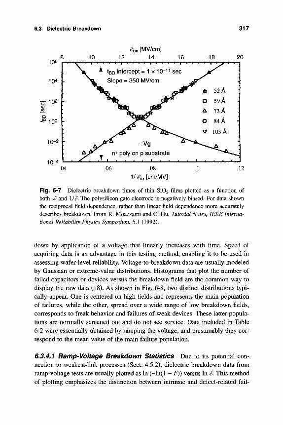
6.3 Dielectric Breal(down 317
106
104 I
-O 102 h 0)
.0).
Q
^ 100
10-2
10 (Tox [MV/cm]
12 14 16 18 20
10-4
1 ' ' X ' ' 1
[ h
[ [• I
1 » irt >
^ tsD intercept = 1 x lO-' ''
^ Slope = 350 MV/cm
A / ^ -vg ' ^ n+ poly on p substrate
* 1 f
sec
m i 1
f •• 1 '
i a A
o
V
t .
1 ' j r ' ' 1
52 A ]
59 A H
73 A j
84 A -j
103 A I
11- > 1 i I III
.04 .06 .08 l/cToxlcm/MV]
.12
Fig. 6-7 Dielectric breakdown times of thin SiOi films plotted as a function of both <o and US'. The poly silicon gate electrode is negatively biased. For data shown the reciprocal field dependence, rather than linear field dependence more accurately describes breakdown. From R. Moazzami and C. Hu, Tutorial Notes, IEEE Interna-tional Reliability Physics Symposium, 5.1 (1992).
down by application of a voltage that linearly increases with time. Speed of acquiring data is an advantage in this testing method, enabling it to be used in assessing wafer-level reliability. Voltage-to-breakdown data are usually modeled by Gaussian or extreme-value distributions. Histograms that plot the number of failed capacitors or devices versus the breakdown field are the common way to display the raw data (18). As shown in Fig. 6-8, two distinct distributions typi-cally appear. One is centered on high fields and represents the main population of failures, while the other, spread over a wide range of low breakdown fields, corresponds to freak behavior and failures of weak devices. These latter popula-tions are normally screened out and do not see service. Data included in Table 6-2 were essentially obtained by ramping the voltage, and presumably they cor-respond to the mean value of the main failure population.
6.3.4.1 Ramp-Voltage Breakdown Statistics Due to its potential con-nection to weakest-link processes (Sect. 4.5.2), dielectric breakdown data from ramp-voltage tests are usually plotted as In (-ln(l - F)) versus In (o. This method of plotting emphasizes the distinction between intrinsic and defect-related fail-
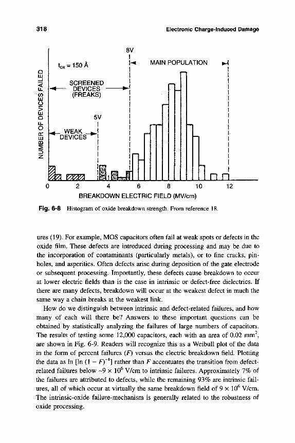
318 Electronic Charge-Induced Damage
Q LLI
0) LLI O > LU Q U. O CC LU
Z
W = 150A
SCREENED DEVICES (FREAKS)
_ WEAK _ DEVICES
IP,
MAIN POPULATION
a n n 0 2 4 6 8 10
BREAKDOWN ELECTRIC FIELD (MV/cm)
Fig. 6-8 Histogram of oxide breakdown strength. From reference 18.
12
ures (19). For example, MOS capacitors often fail at weak spots or defects in the oxide film. These defects are introduced during processing and may be due to the incorporation of contaminants (particularly metals), or to fine cracks, pin-holes, and asperities. Often defects arise during deposition of the gate electrode or subsequent processing. Importantly, these defects cause breakdown to occur at lower electric fields than is the case in intrinsic or defect-free dielectrics. If there are many defects, breakdown will occur at the weakest defect in much the same way a chain breaks at the weakest link.
How do we distinguish between intrinsic and defect-related failures, and how many of each will there be? Answers to these important questions can be obtained by statistically analyzing the failures of large numbers of capacitors. The results of testing some 12,000 capacitors, each with an area of 0.02 mm^, are shown in Fig. 6-9. Readers will recognize this as a Weibull plot of the data in the form of percent failures (F) versus the electric breakdown field. Plotting the data as In [In (1 - F)~^\ rather than F accentuates the transition from defect-related failures below ~9 x 10^ V/cm to intrinsic failures. Approximately 7% of the failures are attributed to defects, while the remaining 93% are intrinsic fail-ures, all of which occur at virtually the same breakdown field of 9 x 10^ V/cm. The intrinsic-oxide failure-mechanism is generally related to the robustness of oxide processing.
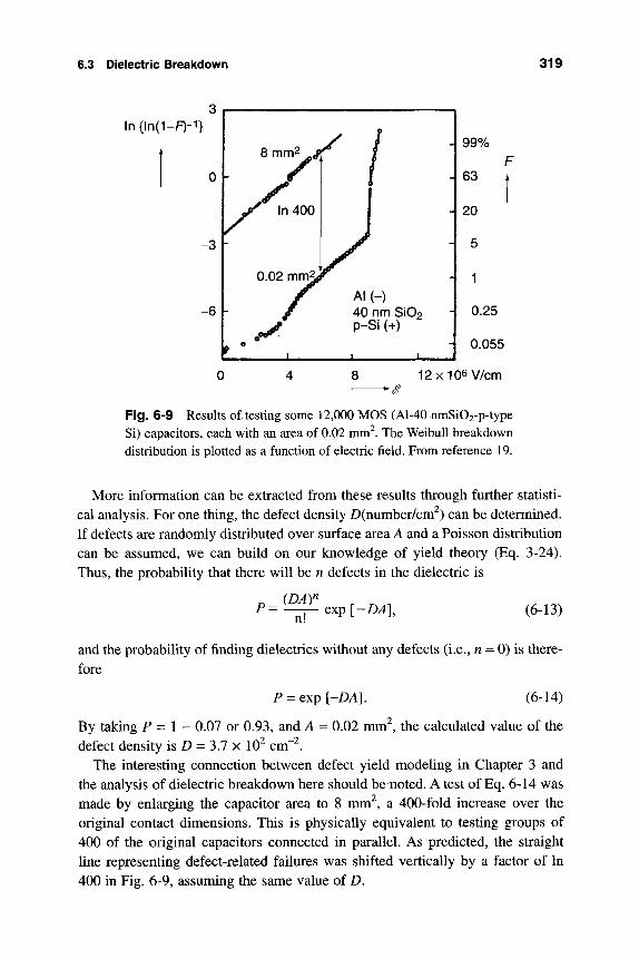
6.3 Dielectric Breal(down 319
In{ln(1-F)-1}
8 12x106V/cm
Fig. 6-9 Results of testing some 12,000 MOS (Al-40 nmSi02-p-type Si) capacitors, each with an area of 0.02 mm . The Weibull breakdown distribution is plotted as a function of electric field. From reference 19.
More information can be extracted from these results through further statisti-cal analysis. For one thing, the defect density D(number/cm^) can be determined. If defects are randomly distributed over surface area A and a Poisson distribution can be assumed, we can build on our knowledge of yield theory (Eq. 3-24). Thus, the probability that there will be n defects in the dielectric is
(DA)^ P=^-~^xp[-DAl (6-13)
and the probability of finding dielectrics without any defects (i.e., n = 0) is there-fore
P = exp[-DA]. (6-14)
By taking P=l- 0.07 or 0.93, and A = 0.02 nmi^, the calculated value of the defect density is D = 3.7 x 10^ cm"^.
The interesting connection between defect yield modeling in Chapter 3 and the analysis of dielectric breakdown here should be noted. A test of Eq. 6-14 was made by enlarging the capacitor area to 8 mm^, a 400-fold increase over the original contact dimensions. This is physically equivalent to testing groups of 400 of the original capacitors connected in parallel. As predicted, the straight line representing defect-related failures was shifted vertically by a factor of In 400 in Fig. 6-9, assuming the same value of D.
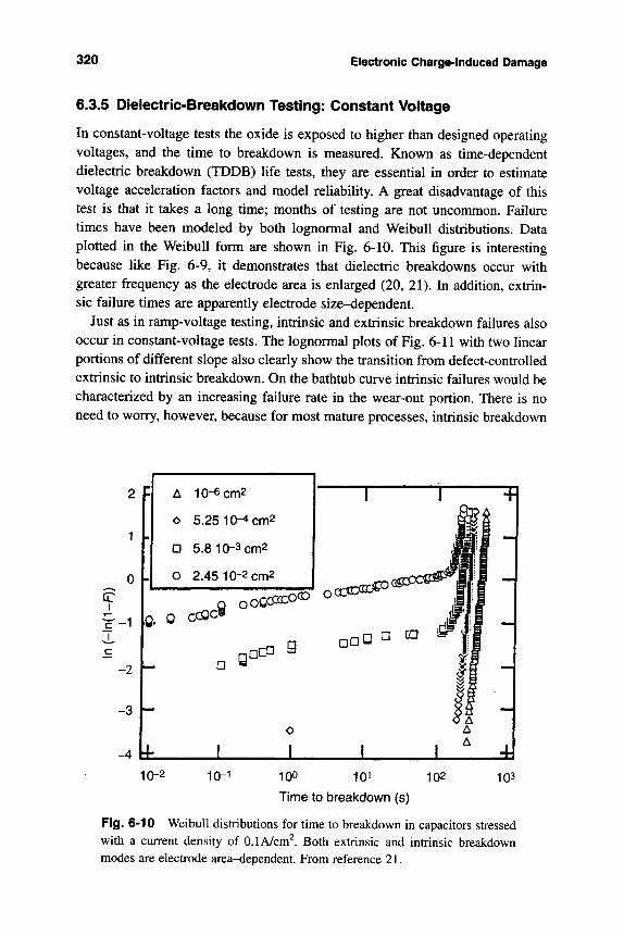
320 Electronic Charge-Induced Damage
6.3.5 Dielectric-Breakdown Testing: Constant Voitage
In constant-voltage tests the oxide is exposed to higher than designed operating voltages, and the time to breakdown is measured. Known as time-dependent dielectric breakdown (TDDB) life tests, they are essential in order to estimate voltage acceleration factors and model reliability. A great disadvantage of this test is that it takes a long time; months of testing are not uncommon. Failure times have been modeled by both lognormal and Weibull distributions. Data plotted in the Weibull form are shown in Fig. 6-10. This figure is interesting because like Fig. 6-9, it demonstrates that dielectric breakdowns occur with greater frequency as the electrode area is enlarged (20, 21). In addition, extrin-sic failure times are apparently electrode size-dependent.
Just as in ramp-voltage testing, intrinsic and extrinsic breakdown failures also occur in constant-voltage tests. The lognormal plots of Fig. 6-11 with two linear portions of different slope also clearly show the transition from defect-controlled extrinsic to intrinsic breakdown. On the bathtub curve intrinsic failures would be characterized by an increasing failure rate in the wear-out portion. There is no need to worry, however, because for most mature processes, intrinsic breakdown
2
1
0
I T—
-2
-4
A 10-6cm2
o 5.25 10-4 cm2
D 5.8 10-3 cm2
O 2.45 10-2 cm2
.Q. 0 ccOd Q OOCCCCDOCD
Q QCP
)GCCDar.€0
• D Q ^ ^°
o
J. 10-2 10-1 100 101 102
Time to breakdown (s)
103
Fig. 6-10 Weibull distributions for time to breakdown in capacitors stressed with a current density of O.lA/cm^. Both extrinsic and intrinsic breakdown modes are electrode area-dependent. From reference 21.
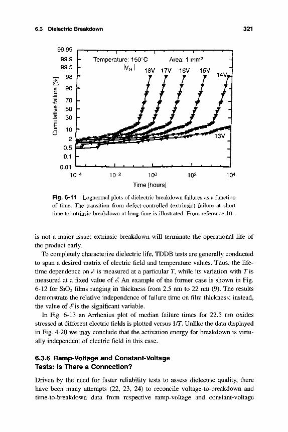
6.3 Dielectric Breal(down 321
99.99
99.9 99.5
98
I I ' ^ ' * ' I
f- Temperature: 150°C
IVG'
0.01 10-4
"T Area: 1 mm2
18V 17V 16V 15V 14Vi
J .
10-2 100
Time [hours]
102 104
Fig. 6-11 Lognormal plots of dielectric breakdown failures as a function of time. The transition from defect-controlled (extrinsic) failure at short time to intrinsic breakdown at long time is illustrated. From reference 10.
is not a major issue; extrinsic breakdown will terminate the operational life of the product early.
To completely characterize dielectric life, TDDB tests are generally conducted to span a desired matrix of electric field and temperature values. Thus, the life-time dependence on S is measured at a particular T, while its variation with T is measured at a fixed value of i. An example of the former case is shown in Fig. 6-12 for Si02 films ranging in thickness from 2.5 nm to 22 nm (9). The results demonstrate the relative independence of failure time on film thickness; instead, the value of cf is the significant variable.
In Fig. 6-13 an Arrhenius plot of median failure times for 22.5 nm oxides stressed at different electric fields is plotted versus 1/7. Unlike the data displayed in Fig. 4-20 we may conclude that the activation energy for breakdown is virtu-ally independent of electric field in this case.
6.3.6 Ramp-Voltage and Constant-Voltage Tests: Is There a Connection?
Driven by the need for faster reliability tests to assess dielectric quality, there have been many attempts (22, 23, 24) to reconcile voltage-to-breakdown and time-to-breakdown data from respective ramp-voltage and constant-voltage
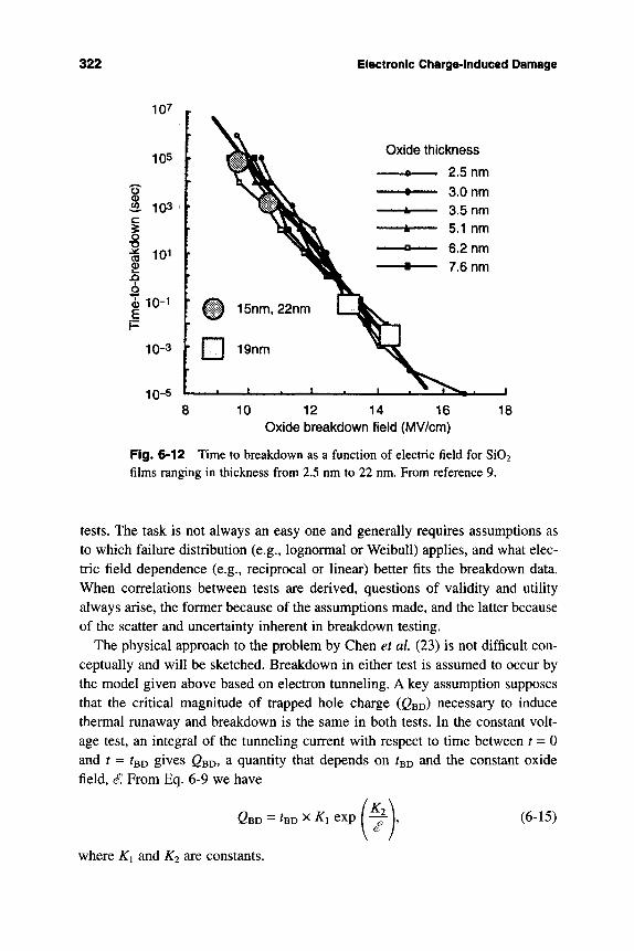
322 Electronic Gharge lnduced Dtmige
Oxide thickness
2.5 nm
3.0 nm 3.5 nm 5.1 nm
6.2 nm 7.6 nm
10 12 14 16 Oxide breakdown field (MV/cm)
18
Fig. 6-12 Time to breakdown as a function of electric field for Si02 films ranging in thickness from 2.5 nm to 22 nm. From reference 9.
tests. The task is not always an easy one and generally requires assumptions as to which failure distribution (e.g., lognormal or Weibull) applies, and what elec-tric field dependence (e.g., reciprocal or linear) better fits the breakdown data. When correlations between tests are derived, questions of validity and utility always arise, the former because of the assumptions made, and the latter because of the scatter and uncertainty inherent in breakdown testing.
The physical approach to the problem by Chen et al. (23) is not difficult con-ceptually and will be sketched. Breakdown in either test is assumed to occur by the model given above based on electron tunneling. A key assumption supposes that the critical magnitude of trapped hole charge (QBY^) necessary to induce thermal runaway and breakdown is the same in both tests. In the constant volt-age test, an integral of the tunneling current with respect to time between r = 0 and t = BD gives J2BD» a quantity that depends on /BD ^^d the constant oxide field, (o. From Eq. 6-9 we have
GBD = BD X ^1 exp ( - ^ 1, (6-15)
where Ki and K2 are constants.
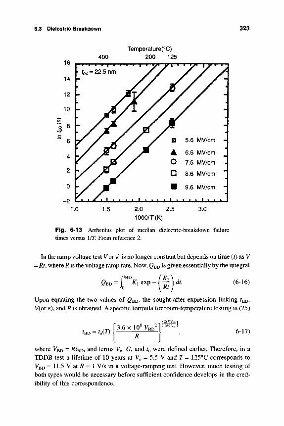
6.3 Dieiectric Breakdown 323
400 Temperature(°C)
200 12S
2.0 2.5 1000/T(K)
Fig. 6-13 Arrhenius plot of median dielectric-breakdown failure times versus VT, From reference 2.
In the ramp voltage test Vor <f is no longer constant but depends on time (0 as V - Rt, where R is the voltage ramp rate. Now, Q^D is given essentially by the integral
Q^o = j^''K,cxp-l^\dt. (6-16)
Upon equating the two values of QBD. the sought-after expression linking t^i,, V(or e), and R is obtained. A specific formula for room-temperature testing is (25)
^^^^ |3 .6x lO-V3p G{T)\/sDl 350 V„ J
R I 6-17)
where VBD - Rhvy ^nd terms VQ, G, and t^ were defined earlier. Therefore, in a TDDB test a lifetime of 10 years at V^ = 5.5 V and 7 = 125X corresponds to VBD = 1 1 . 5 V a t / ? = l V/s in a voltage-ramping test. However, much testing of both types would be necessary before sufficient confidence develops in the cred-ibility of this correspondence.
324 Electronic Charge-Induced Damage
6.3.7 Electric-Field and Temperature-Acceleration Factors
The electric-field acceleration factor, y, is defined as the negative slope of the log BD vs i plot derived from constant voltage testing. As a consequence of Eq.
6-10, the reciprocal electric field model yields
t/[log^BD]
while for the linear field model,
In 10 S'
Y = G L .
(decades/MV/cm), (6-18)
(6-19)
Therefore, while y is predicted to be dependent on the electric field according to Eq. 6-18, it assumes a constant value, irrespective of the field, in linear field modeling. The results of investigations over the years (23, 25) typically show that y = 6 decades per MV/cm when (^« 5 MV/cm, and roughly 1.5 decades per MV/cm when cf == 10 MV/cm. Thus, the reciprocal breakdown-field model bet-ter accounts for the wide variation in y values reported in the literature.
The temperature acceleration factor, AF(r), is field-dependent in both models. For fixed electric field testing.
^ p . ^ ^ ^BD(7^I) _ toiJx) exp \G{J,)IS\ tBD(T2) UT2)txp[G(T2)/cti'
(6-20)
Accounting for the temperature dependence of both to and G at temperatures Ti and T2, the result for the reciprocal field case is
EBD/ 1 1 k \T2
AF(T) = exp
Similarly, for the linear field model,
AF(7) = exp
Ti exp [GR(rO - Gj,(T2)]
(6-21)
{Qxp[GdTO(^BD(Ti) - i ) - GdT2)){iBx,iT2) - i)]}. (6-22)
In this case the temperature acceleration factor depends on T and (f in a complex way.
If one assumes that the exponential term within each second pair of brackets is weakly temperature-dependent relative to the first exponent, then we are left with the simple Boltzmann acceleration factor
AF(7) = exp (6-23)
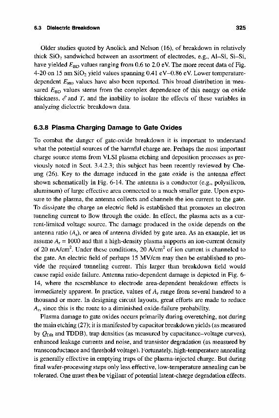
6.3 Dielectric Breal(down 325
Older studies quoted by Anolick and Nelson (16), of breakdown in relatively thick Si02 sandwiched between an assortment of electrodes, e.g., Al-Si, Si-Si, have yielded E^j) values ranging from 0.6 to 2.0 eV. The more recent data of Fig. 4-20 on 15 nm Si02 yield values spanning 0.41 eV-0.86 eV. Lower temperature-dependent E^D values have also been reported. This broad distribution in mea-sured ^BD values stems from the complex dependence of this energy on oxide thickness, S' and T, and the inability to isolate the effects of these variables in analyzing dielectric breakdown data.
6.3.8 Plasma Charging Damage to Gate Oxides
To combat the danger of gate-oxide breakdown it is important to understand what the potential sources of the harmful charge are. Perhaps the most important charge source stems from VLSI plasma etching and deposition processes as pre-viously noted in Sect. 3.4.2.3; this subject has been recently reviewed by Che-ung (26). Key to the damage induced in the gate oxide is the antenna effect shown schematically in Fig. 6-14. The antenna is a conductor (e.g., polysilicon, aluminum) of large effective area connected to a much smaller gate. Upon expo-sure to the plasma, the antenna collects and channels the ion current to the gate. To dissipate the charge an electric field is established that promotes an electron tunneling current to flow through the oxide. In effect, the plasma acts as a cur-rent-limited voltage source. The damage produced in the oxide depends on the antenna ratio (A ), or area of antenna divided by gate area. As an example, let us assume Aj. = 1000 and that a high-density plasma supports an ion-current density of 20 mA/cm^. Under these conditions, 20 A/cm^ of ion current is channeled to the gate. An electric field of perhaps 15 MV/cm may then be established to pro-vide the required tunneling current. This larger than breakdown field would cause rapid oxide failure. Antenna ratio-dependent damage is depicted in Fig. 6-14, where the resemblance to electrode area-dependent breakdown effects is immediately apparent. In practice, values of A range from several hundred to a thousand or more. In designing circuit layouts, great efforts are made to reduce Af, since this is the route to a diminished oxide-failure probability.
Plasma damage to gate oxides occurs primarily during overetching, not during the main etching (27); it is manifested by capacitor breakdown yields (as measured by QDB and TDDB), trap densities (as measured by capacitance-voltage curves), enhanced leakage currents and noise, and transistor degradation (as measured by transconductance and threshold voltage). Fortunately, high-temperature annealing is generally effective in emptying traps of the plasma-injected charge. But during final wafer-processing steps only less effective, low-temperature annealing can be tolerated. One must then be vigilant of potential latent-charge degradation effects.
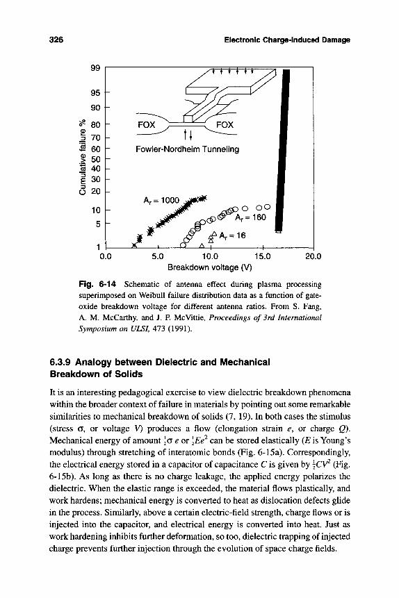
326 Electronic Charge-induced Damage
99
95
90 H
80 70 60
_ 50 ^ 40 I 30 d 20
10
5
0.0
M M U
Fowler-Nordheim Tunneling
A r=1000 jp * ^ o o o
Ar=160
- - ^^ - I -5.0 10.0 15.0
Breakdown voltage (V) 20.0
Fig. 6-14 Schematic of antenna effect during plasma processing superimposed on Weibull failure distribution data as a function of gate-oxide breakdown voltage for different antenna ratios. From S. Fang, A. M. McCarthy, and J. P. McVittie, Proceedings of 3rd International Symposium on ULSI, 473 (1991).
6.3.9 Analogy between Dielectric and IMechanical Breakdown of Solids
It is an interesting pedagogical exercise to view dielectric breakdown phenomena within the broader context of failure in materials by pointing out some remarkable similarities to mechanical breakdown of solids (7, 19). In both cases the stimulus (stress a, or voltage V) produces a flow (elongation strain e, or charge Q). Mechanical energy of amount \c e or \Ee^ can be stored elastically (E is Young's modulus) through stretching of interatomic bonds (Fig. 6-15a). Correspondingly, the electrical energy stored in a capacitor of capacitance C is given by \CV^ (Fig. 6-15b). As long as there is no charge leakage, the applied energy polarizes the dielectric. When the elastic range is exceeded, the material flows plastically, and work hardens; mechanical energy is converted to heat as dislocation defects glide in the process. Similarly, above a certain electric-field strength, charge flows or is injected into the capacitor, and electrical energy is converted into heat. Just as work hardening inhibits further deformation, so too, dielectric trapping of injected charge prevents further injection through the evolution of space charge fields.
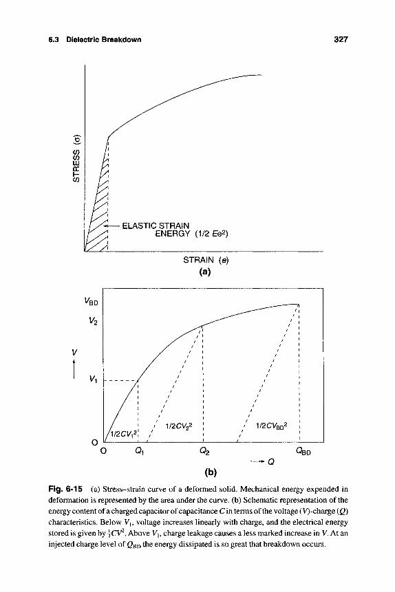
6.3 Dielectric Breakdown 327
- ELASTIC STRAIN ENERGY (1/2 Ee2)
STRAIN (e)
(a)
V'BD
Va
Vi
r\ / l /2C^2
/ f / 1
( 1
1
1 /
1
' MZCV.^ t
. . , , ,t , , .„, ,„,,,„,. .,
^ — — " ^ ' 1
"— ' 1 '
/ 1 / 1
/ 1
/ 1 / ,
/ . /
/
/ 1
/ 1
1 1/2CVBD2
! .,/ ., -
Qi © 2
(b)
^ D Q
Fig. 6-15 (a) Stress-strain curve of a deformed solid. Mechanical energy expended in deformation is represented by the area under the curve, (b) Schematic representation of the energy content of a charged capacitor of capacitance C in terms of the voltage (V)-charge ( 0 characteristics. Below Vj, voltage increases linearly with charge, and the electrical energy stored is given by |CV^, Above Vi, charge leakage causes a less marked increase in V. At an injected charge level of QBD the energy dissipated is so great that breakdown occurs.
328 Electronic Charge-Induced Damage
When the strains or injected charge levels exceed critical values, failure occurs, and the material suddenly loses part or all of the stored energy. In mechanics we speak of fracture, while in dielectrics, breakdown occurs. Instead of statically applied loads, dynamic stresses of low amplitudes are known to cause fatigue. The analogous phenomenon in dielectrics is known as treeing, a damage process briefly discussed in the next section.
There is yet another parallel between the effects of straining and charge injection rates on failure. Solids strained slowly generally exhibit greater elongations to fail-ure than when strained very rapidly. Fractures are often ductile below and brittle above a roughly defined transition strain-rate level. In the dielectric analogue, the charge stored to breakdown (2BD) decreases abruptly beyond a certain injection rate. Above the transition injection rate, charge apparently accumulates more rapidly than it can be dissipated. In the mechanical case we would say that a ductile-to-brittle transition occurs because the system is straining faster than it can relax.
In sunmiary, we may regard dielectrics as "ductile" materials when QBD is large. In such a case the matrix can dissipate a large amount of energy, and QBD is orders of magnitude larger than the displacement charge D(q). For "brittle" dielectrics, in contrast, CBD is not much larger than D(q).
6.3.10 Discharges and Water Trees
Realizing that electrical breakdown of insulation is not limited to thin films and microelectronics, it is instructive to end our formal discussion of dielectric break-down with examples drawn from bulk glasses and polymers. Consider the dramatic lightning-like discharge in glass captured in the photograph of Fig. 6-16. This so-called Lichtenberg discharge occurred as the result of exposing the glass block to high-energy radiation and grounding it. Prior to breakdown, injected electrons accumulate in the solid, causing a kind of dielectric wear. Like rivers eroding the earth, the damage spreads as electrons preferentially lose their energy at previously damaged sites. Just as small streams form broad rivers that leave deep channels in the landscape, so too, leaking charge wears away the insulator until a low resistance path between electrodes ultimately causes destruction of the capacitor. Erosion wear is apparently not related to the rate of water (charge) flow, but only to the accu-mulated volume (amount). Such a damage model applies, in principle, to thin gate oxides, but such tree-like discharge patterns have apparently not been reported.
It has been more than a quarter century since the morphologically similar phe-nomenon of water treeing was first observed in cable insulation (28). Water trees grow in a wide range of hydrophobic-polymeric insulating materials, e.g., extruded polyethylene, when exposed to both moisture and high voltage. The bush or tree-like growths within the polymer result in lower dielectric-break-
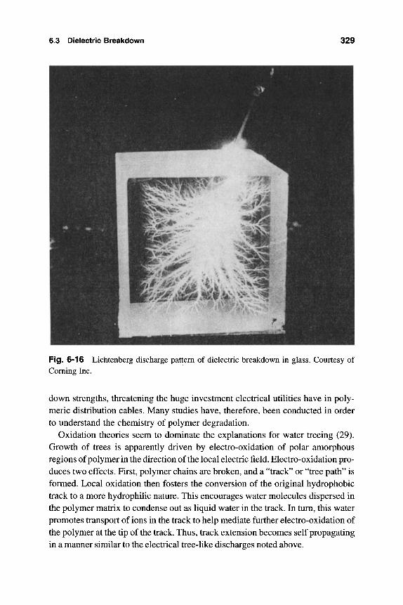
6.3 Dielectric Breakdown 329
Fig, 6-16 Lichtenberg discharge pattern of dielectric breakdown in glass. Courtesy of Coming Inc.
down strengths, threatening the huge investment electrical utilities have in poly-meric distribution cables. Many studies have, therefore, been conducted in order to understand the chemistry of polymer degradation.
Oxidation theories seem to dominate the explanations for water treeing (29). Growth of trees is apparently driven by electro-oxidation of polar amorphous regions of polymer in the direction of the local electric field. Electro-oxidation pro-duces two effects. First, polymer chains are broken, and a "track" or "tree path" is formed. Local oxidation then fosters the conversion of the original hydrophobic track to a more hydrophilic nature. This encourages water molecules dispersed in the polymer matrix to condense out as liquid water in the track. In turn, this water promotes transport of ions in the track to help mediate further electro-oxidation of the polymer at the tip of the track. Thus, track extension becomes self propagating in a manner similar to the electrical tree-like discharges noted above.
330 EleGtrontc Charge-lfiduced j^magt
6.4 HOT-^CARRIER EFFECTS
6.4.1 Introduction
Chajrge that is injected into the gate oxide is a concern because the switching characteristics of a MOSFET can degrade and exhibit instabilities as a result. When a MOSFET acts as a good switch, the drain-source current is as large as possible in the on state and very low in the off state* The typical effect of hot-carrier, or commonly hot-electron, degradation is to reduce the on-state current in an n-MOSFET and increase the off-state current in a p-MOSFET (30) (see Fig. 2-17). A measure of transistor degradation or lifetime is commonly defined in terms of some percentage shift of threshold voltage, change in transconduc-tance, or variation in drive or saturation current* To understand the origin of these effects we start with a discussion of the nature of hot electrons. The observed degradation of device characteristics will then be discussed and inter-preted in terms of models for hot-carrier effects.
6.4.2 Hot Carriers
For semiconductors in thermal equilibrium, electrons and holes continually absorb and emit acoustical phonons (low-frequency lattice vibrations), resulting in an average energy gain of zero. Such electrons have kinetic energies (£) that are normally slightly higher than that of the conduction band edge (EQ) by an amount -kT^. Similarly, for holes, E is slightly less than the valence band edge (Ey), again by -kT^. At room temperature (7 ), kT^^ is only 0*025 eV, which is small compared to the carrier kinetic energy corresponding to EQ and Ey. This is the case in low electric fields, where the carrier velocity is field-independent (Ohm's law). Under nonequilibrium conditions, however, carriers with far larger kinetic energies con-tribute to the current flow. In electric fields of 20 kV/cm, for example, the carriers lose energy by scattering with optical or high-frequency phonons, and their veloc-ities saturate at roughly 10 cm/s. But at fields of 100 kV/cm, carriers gain more energy than they lose by scattering. Such accelerated electrons have energies of EQ + kTe, where T^ is an effective temperature such that kT^ > kT^, With effective temperatures (-Ec/kT) of tens of thousands of degrees Kelvin, these electrons are at the very top of the Fermi distribution. Known as hot electrons, they pose seri-ous reliability problems in MOS transistors (4).
Consider now the MOS structure with a current that flows through the silicon channel parallel to the Si-Si02 interface. As long as they remain in the Si, hot carriers cause no damage. But during scattering they may acquire a transverse component of velocity that enables them to enter the adjacent oxide. Such charge
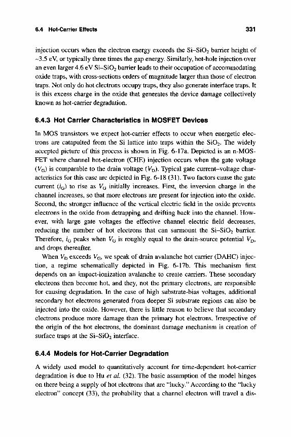
6.4 Hot-Carrier Effects 331
injection occurs when the electron energy exceeds the Si-Si02 barrier height of -3.5 eV, or typically three times the gap energy. Similarly, hot-hole injection over an even larger 4.6 eV Si-Si02 barrier leads to their occupation of acconmiodating oxide traps, with cross-sections orders of magnitude larger than those of electron traps. Not only do hot electrons occupy traps, they also generate interface traps. It is this excess charge in the oxide that generates the device damage collectively known as hot-carrier degradation.
6.4.3 Hot Carrier Characteristics in IMOSFET Devices
In MOS transistors we expect hot-carrier effects to occur when energetic elec-trons are catapulted from the Si lattice into traps within the Si02. The widely accepted picture of this process is shown in Fig. 6-17a. Depicted is an n-MOS-FET where channel hot-electron (CHE) injection occurs when the gate voltage (VQ) is comparable to the drain voltage (VD). Typical gate current-voltage char-acteristics for this case are depicted in Fig. 6-18 (31). Two factors cause the gate current ((Q) to rise as VQ initially increases. First, the inversion charge in the channel increases, so that more electrons are present for injection into the oxide. Second, the stronger influence of the vertical electric field in the oxide prevents electrons in the oxide from detrapping and drifting back into the channel. How-ever, with large gate voltages the effective channel electric field decreases, reducing the number of hot electrons that can surmount the Si-Si02 barrier. Therefore, IQ peaks when VQ is roughly equal to the drain-source potential Vo» and drops thereafter.
When VD exceeds VG^ we speak of drain avalanche hot carrier (DAHC) injec-tion, a regime schematically depicted in Fig. 6-17b. This mechanism first depends on an impact-ionization avalanche to create carriers. These secondary electrons then become hot, and they, not the primary electrons, are responsible for causing degradation. In the case of high substrate-bias voltages, additional secondary hot electrons generated from deeper Si substrate regions can also be injected into the oxide. However, there is little reason to believe that secondary electrons produce more damage than the primary hot electrons. Irrespective of the origin of the hot electrons, the dominant damage mechanism is creation of surface traps at the Si-Si02 interface.
6.4.4 IModels for IHot-Carrier Degradation
A widely used model to quantitatively account for time-dependent hot-carrier degradation is due to Hu et al (32). The basic assumption of the model hinges on there being a supply of hot electrons that are "lucky." According to the "lucky electron" concept (33), the probability that a channel electron will travel a dis-
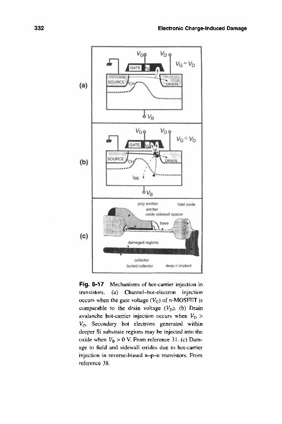
332 Electronic Charge-Induced Damage
(a)
(b)
(c)
VGO VD
^3=^4)
Til UGO VO
1/G<\/D
poly emitter field emitter oxide sidewall spacer
collector
buried collector deep n implant
Fig. 6-17 Mechanisms of hot-carrier injection in transistors, (a) Channel-hot-electron injection occurs when the gate voltage (VG) of n-MOSFET is comparable to the drain voltage (VD)- (b) Drain avalanche hot-carrier injection occurs when VQ > VQ. Secondary hot electrons generated within deeper Si substrate regions may be injected into the oxide when VB > 0 V. From reference 31. (c) Dam-age to field and sidewall oxides due to hot-carrier injection in reverse-biased n-p-n transistors. From reference 38.
6.4 Hot-Carrier Effects 333
10-10
10-11
o
3 10-12
4—• CO
O
10-13
10-14
fox = 20 nm
Leff = 0.8^im
r = 300°K
L r=355°K Ii
t i i
12
Fig. 6-18 Gate current-voltage characteristics for hot-carrier injection by the channel-hot-electron injection mechanism. From reference 31.
tance d or more without suffering any collision is equal to exp [-dlX\, where X is the mean free path between scattering events. Now consider an electron of charge q, traveling a distance X in the channel electric field S^- The probability that it will reach energy (j) without suffering a collision is given by exp [-^l(k q 4)] , because d = ^l{q 4) . For channel electrons to reach the gate oxide, two "lucky" processes are involved. The first requires that electrons gain sufficient kinetic energy from the channel field to become hot. Secondly, the electron momentum must be redirected perpendicularly, so that hot electrons can enter the oxide. The explicit consequences of these processes are substrate (/s) and
334 Electronic Charge-Induced Damage
gate currents (^G) whose magnitudes depend on electron energies reaching those required for impact ionization (^i), and for surmounting the Si-Si02 energy bar-rier ((j)b), respectively. In particular.
- * i
XqS'c is = ^I'D exp
and
h = Q ' D exp XqS'c
(6-24)
(6-25)
where Ci and C2 are constants. In these equations, /^ is the (cold) drain current flow that supplies some of the eventually "lucky" electrons. Eliminating X qS^ from Eqs. 6-24 and 25 yields
^ - C , y ^ , (6-26)
where m = <t)b/<t>i- This equation, which applies to the case where VG exceeds VD^ has been verified in w-channel transistors. It is found that m is approximately 3, which is roughly consistent with values of (t)i « 1.3 eV and (t)b « 3.5 eV.
In normal MOSFET operation the gate current is negligible and barely mea-surable. When hot electrons are generated, /Q rises rapidly, as seen in the char-acteristics of Fig. 6-18, thus providing a good measure of the ensuing damage. To link the gate current to time-dependent degradation, let us denote the shift, change, or variation in electrical parameter due to hot-carrier effects by A. If the time (0 rate of change in A is proportional to IQ, then
d^ ^A(A) / / s r . . . 7 , — ^io--^i.\-y (6-27)
Here W is the MOSFET width, and A(A) has absorbed C2 and Ci and addition-ally accounts for the dependence of degradation on existing damage. When dA/dt reaches a certain level, we say that hot-carrier failure has occurred. Since the time to failure (MTTF) depends on the reciprocal of d/^dt,
MTTF"^ = Bij^ i ^ , (6-28)
where B = A{d^lW. A test of this equation is made in Fig. 6-19 (34) for different devices operating under a wide variety of static and dynamic operating condi-tions. Here device lifetime is defined as the time it takes for the drain current to decrease by 5%. In this case a slope of -1 is obtained.
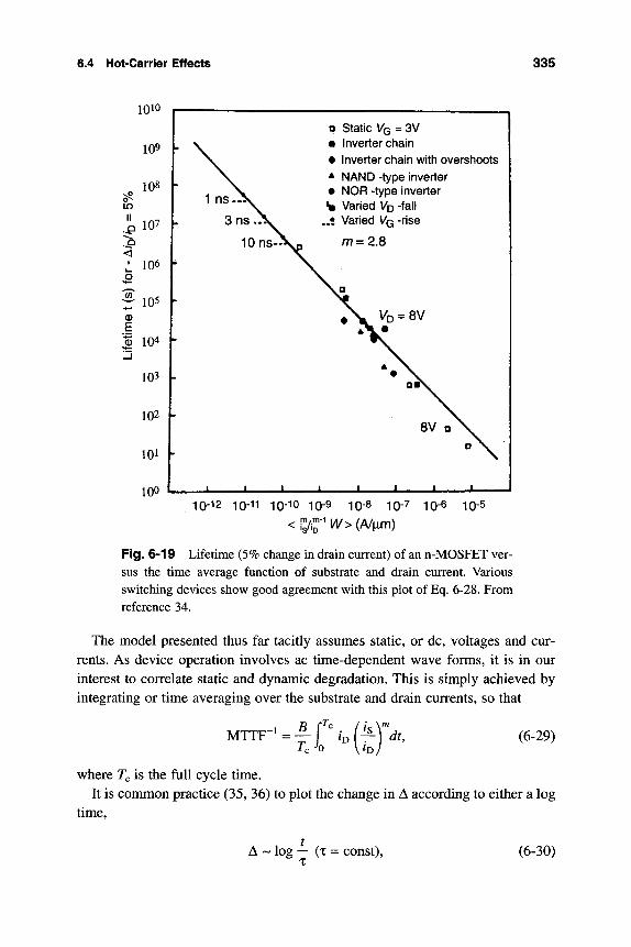
6.4 Hot-Carrier Effects 335
10-12 10-11 10-10 10-9 10-8 10-7 10-6 10-5 ^ I I I / I I I - ' 1/1/> (A/|im)
Fig. 6-19 Lifetime (5% change in drain current) of an n-MOSFET ver-sus the time average function of substrate and drain current. Various switching devices show good agreement with this plot of Eq. 6-28. From reference 34.
The model presented thus far tacitly assumes static, or dc, voltages and cur-rents. As device operation involves ac time-dependent wave forms, it is in our interest to correlate static and dynamic degradation. This is simply achieved by integrating or time averaging over the substrate and drain currents, so that
M T T F - ^ = - | ^ r % D ( - p ^ (6-29)
where T^ is the full cycle time. It is conmion practice (35, 36) to plot the change in A according to either a log
time.
A - log — (X- const), (6-30)
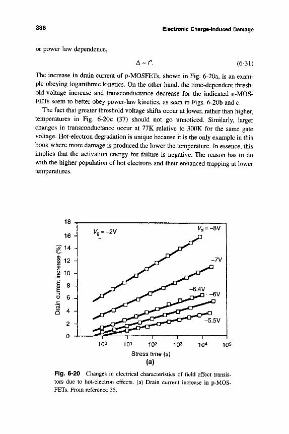
336 Electronic Charge-Induced Damage
or power law dependence,
^'-f. (6-31)
The increase in drain current of p-MOSFETs, shown in Fig. 6-20a, is an exam-ple obeying logarithmic kinetics. On the other hand, the time-dependent thresh-old-voltage increase and transconductance decrease for the indicated n-MOS-FETs seem to better obey power-law kinetics, as seen in Figs. 6-20b and c.
The fact that greater threshold voltage shifts occur at lower, rather than higher, temperatures in Fig. 6-20c (37) should not go unnoticed. Similarly, larger changes in transconductance occur at 77K relative to 300K for the same gate voltage. Hot-electron degradation is unique because it is the only example in this book where more damage is produced the lower the temperature. In essence, this implies that the activation energy for failure is negative. The reason has to do with the higher population of hot electrons and their enhanced trapping at lower temperatures.
T 101 102 103
Stress time (s) (a)
104 105
Fig. 6-20 Changes in electrical characteristics of field effect transis-tors due to hot-electron effects, (a) Drain current increase in p-MOS-FETs. From reference 35.
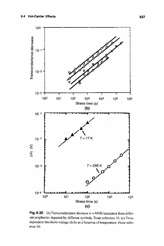
6.4 Hot-Carrier Effects 337
-T 1 \ 1 r 100 101 102 103 104 105 106
Stress time (s)
(b)
<
10-1
10-2
10-3
in-4 '
^ f T f f f H 1 |
f-
k
»
• > a, i i i i i i i
f f
X
i i
> - * \
r=77K
r=295K
V o/
^
J
4
H P i J
J
r 1 100 104 101 102 103
stress time (s)
(c) Fig. 6-20 (b) Transconductance decrease in n-MOS transistors from differ-ent prophecies depicted by different symbols. From reference 35. (c) Time-dependent threshold-voltage shifts as a'ftmction of temperature. From refer-ence 36.
338 Electronic Charge-Induced Demeit
6.4.5 Hot-Carrier Damage in Otiier Devices
Hot'Carrier effects are not limited to MOSFETs. They also occur in n-p-n as well as p-n-p Si bipolar transistors. In particular, bipolar transistors used in read/write amplifiers suffer loss in current gain when subjected to reverse emit-ter-base voltage stress. Apparently the oxide regions adjacent to the emitter-base become damaged due to electron trapping at interface states, an effect that raises the base current, thus lowering the transistor gain. Models for the leakage-cur-rent paths through the oxide sidewall spacer and field-oxide ("birdsbeak") struc-tures are depicted in Fig. 6-17c, It has been observed that the change in base cur-rent (AIB) with time (0 is linear for short times, but AJB ~ t^'^ for longer times, indicating partial saturation (39), The transition in degradation kinetics occurs after a characteristic time x given by x = To exp [-VEB/VQ], where VEB is the reverse emitter-base voltage; values for x© and VQ depend on the particular device and are typically 5 x 10"* s and 0.25 V, respectively.
Degradation of GaAs-based MESFET and HEMT devices due to hot electrons has also been reported (39). In the case of HEMTs these effects show up at large drain-source voltages that enable carriers to reach high energies and cause impact-ionization effects. As a result, the drain current decreases, the parasitic drain-resistance increases, and there is a change in the transconductance fre-quency response.
6.4.6 Combating Hot-Carrier Damage
Basic to a number of processing strategies for minimizing hot-carrier effects in n-MOSFETs is the introduction of ion implanted regions of lighter doping between the channel and heavily doped drain regions. This doped-substrate engi-neering is accomplished through double diffused drain (DDD), lightly doped drain (LDD), and large angle tilt implanted drain (LATID) structures. As a con-sequence of these creatively altered doping profiles, the electric field is spread out, reducing its peak value.
Additional approaches to increasing immunity to hot-carrier damage involve thermochemical processing. In an effort to reduce the Si-Si02 interfacial trap density, postmetallization anneals at '-400°C are commonly carried out in hydro-gen. This improves device function by passivating interface states that are oth-erwise active. However, under the stimulus of hot-electron impact it is thought that hydrogen desorbs from the Si-Si02 interface and, in effect, causes the observed degradation. To minimize this possibility and further combat hot-carrier injection, the gate oxide is now lightly nitrided. This dielectric is more resistant to interface-trap generation, presumably because weaker silicon-hydro-gen bonds possessing an energy of 0.5 eV are replaced by stronger silicon-
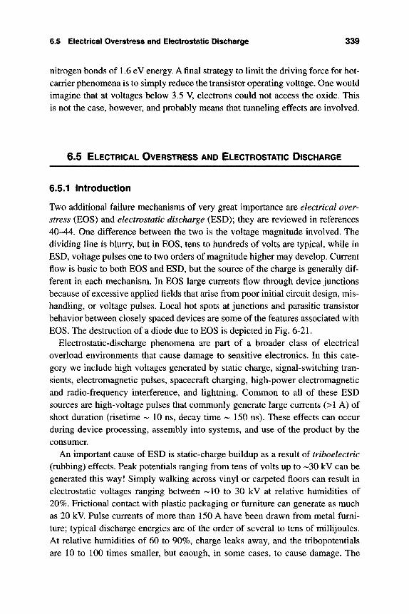
6.5 Eiectrical Overstress and Electrostatic Discharge 339
nitrogen bonds of 1.6 eV energy. A final strategy to limit the driving force for hot-carrier phenomena is to simply reduce the transistor operating voltage. One would imagine that at voltages below 3.5 V, electrons could not access the oxide. This is not the case, however, and probably means that tunneling effects are involved.
6.5 ELECTRICAL OVERSTRESS AND ELECTROSTATIC DISCHARGE
6.5.1 Introduction
Two additional failure mechanisms of very great importance are electrical over-stress (EOS) and electrostatic discharge (ESD); they are reviewed in references 40-44. One difference between the two is the voltage magnitude involved. The dividing line is blurry, but in EOS, tens to hundreds of volts are typical, while in ESD, voltage pulses one to two orders of magnitude higher may develop. Current flow is basic to both EOS and ESD, but the source of the charge is generally dif-ferent in each mechanism. In EOS large currents flow through device junctions because of excessive applied fields that arise from poor initial circuit design, mis-handling, or voltage pulses. Local hot spots at junctions and parasitic transistor behavior between closely spaced devices are some of the features associated with EOS. The destruction of a diode due to EOS is depicted in Fig. 6-21.
Electrostatic-discharge phenomena are part of a broader class of electrical overload environments that cause damage to sensitive electronics. In this cate-gory we include high voltages generated by static charge, signal-switching tran-sients, electromagnetic pulses, spacecraft charging, high-power electromagnetic and radio-frequency interference, and lightning. Common to all of these ESD sources are high-voltage pulses that commonly generate large currents (>1 A) of short duration (risetime -^ 10 ns, decay time --150 ns). These effects can occur during device processing, assembly into systems, and use of the product by the consumer.
An important cause of ESD is static-charge buildup as a result of triboelectric (rubbing) effects. Peak potentials ranging from tens of volts up to '-30 kV can be generated this way! Simply walking across vinyl or carpeted floors can result in electrostatic voltages ranging between '-10 to 30 kV at relative humidities of 20%. Frictional contact with plastic packaging or furniture can generate as much as 20 kV. Pulse currents of more than 150 A have been drawn from metal furni-ture; typical discharge energies are of the order of several to tens of millijoules. At relative humidities of 60 to 90%, charge leaks away, and the tribopotentials are 10 to 100 times smaller, but enough, in some cases, to cause damage. The
340 Electronic Charge-Induced Damage
1 0 K U X 5 , 0 8 0 n 1 6 1 0 0 2
Fig. 6-21 Damage to protection diode device during electrical-overstress testing. Courtesy of M. C. Jon, Lucent Technologies, Bell Laboratories Innovations.
ordering of triboelectric effects in different materials is illustrated in Table 6-3. When two materials in the series are rubbed together, the one that is higher in the series acquires a positive potential relative to the lower one.
In discharges of tens of kV the resulting currents cause indiscriminate dam-age; i.e., failures are not specific to any particular component or device. Oxides, interconnections, contacts, and semiconductor junctions of integrated circuits and electro-optical devices are vulnerable. The sensitivity of a device to ESD generally scales inversely to the minimum-size feature. This can be appreciated with reference to Table 6-4, where discrete devices such as high-speed MOS and compound semiconductor field effect transistors are most sensitive to damage because of their small dimensions.
Depending on the voltage level, speed of approach and shape of charged bodies, signals can exceed 1 gigahertz, and may reach 5 GHz. At these frequencies equip-ment cables and stripes on printed-circuit boards act as efficient receiving antennas. In general, the voltage and current necessary to cause damage is one to two orders of magnitude greater than that to cause a temporary upset (e.g., causing a memory change of 0 to 1 or 1 to 0). Thus, conductive coupling through an ESD spark will destroy circuit lines, whereas radiation coupling may only cause upset.
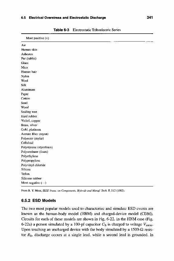
6.5 Electrical Overstress and Electrostatic Discharge 341
Table 6-3 Electrostatic Triboelectric Series
Most positive (+)
Air Human skin Asbestos Fur (rabbit) Glass Mica Human hair Nylon Wool Silk Aluminum Paper Cotton Steel Wood Sealing wax Hard rubber Nickel, copper Brass, silver Gold, platinum Acetate fiber (rayon) Polyester (mylar) Celluloid Polystyrene (styrofoam) Polyurethane (foam) Polyethylene Polypropylene Polyvinyl chloride Silicon Teflon Silicone rubber Most negative (—)
From R. Y. Moss, IEEE Trans, on Components, Hybrids and Manuf. Tech. 5, 512 (1982).
6.5.2 ESD Models
The two most popular models used to characterize and simulate ESD events are known as the human-body model (HBM) and charged-device model (CDM). Circuits for each of these models are shown in Fig. 6-22. In the HBM case (Fig. 6-22a) a person simulated by a 100-pf capacitor C^ is charged to voltage VHBM-Upon touching an uncharged device with the body simulated by a 1500-Q resis-tor R^, discharge occurs at a single lead, while a second lead is grounded. In
342 Electronic Charge-Induced Damage
Table 6-4 Susceptibility of Various Devices to ESD Damage
Device Range of Damage ESD Susceptibility (V)
MOSFET 10-100 GaAsFET 100-300 EPROM 100-500 JFET 140-7000 Surface acoustic wave 150-500 Operational amplifier 190-2500 CMOS 250-3000 Schottky diodes 300-2500 Thin and thick film resistors 300-3000 Bipolar transistors 380-7000 Silicon controlled rectifiers 680-1000 8085 Microprocessor 500-2000
After N. Sclater, Electrostatic Discharge Protection for Electronics, TAB Books, McGraw Hill, Blue Ridge Summit, PA (1990).
evaluating the ESD vulnerability of a device, C^ is first charged to VHBM with switches Si closed and ^2 open. Switch 5*2 is then closed after opening Si, and the capacitor charge (Q = C^ V'HBM) is discharged into the device. If the device being tested has resistance Rj, then Ohm's law gives for the time (0-dependent ac current,
/ (t) = /o exp (6-32)
where i^ = VHBM/(^T + ^B)» and the time constant T = CB (RJ + ^B)- The power P dissipated in resistor Rj is simply
P = i(t)\Rj). (6-33)
Since we are eventually concerned with the resistor temperature rise, the energy discharged is of importance. This energy is partitioned between R^ and Rj, and that dissipated by Rj alone is given by
where £"0 is the energy originally stored in CB, namely, | CB VHBM -
The charged-device model considers the situation where charge initially resides on a device as shown in Fig. 6-22b. This charge may have arrived via tri-boelectric rubbing or sliding in shipping tubes. During simulation testing the
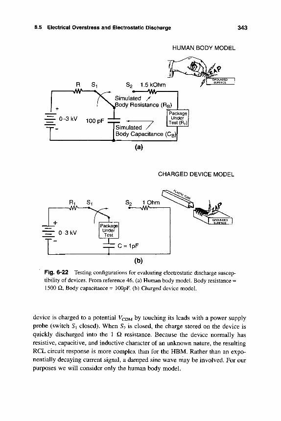
6.5 Electrical Overstress and Electrostatic Discharge 343
HUMAN BODY MODEL
S2 1.5kOhm - — ^ W \ / —
Simulated / Body Resistance (RB)
Simulated / Body Capacitance (CB)|
Package Under
Test (R-r)
(a)
CHARGED DEVICE MODEL
S2 1 Ohm • >/W^
" = r 0-3 kV Package! Under Test
= = C ^ 1 p F
(b)
Fig. 6-22 Testing configurations for evaluating electrostatic discharge suscep-tibility of devices. From reference 46. (a) Human body model. Body resistance = 1500 Q, Body capacitance = lOOpF. (b) Charged device model.
device is charged to a potential VCDM by touching its leads with a power supply probe (switch ^i closed). When 5*2 is closed, the charge stored on the device is quickly discharged into the 1 Q resistance. Because the device normally has resistive, capacitive, and inductive character of an unknown nature, the resulting RCL circuit response is more complex than for the HEM. Rather than an expo-nentially decaying current signal, a damped sine wave may be involved. For our purposes we will consider only the human body model.
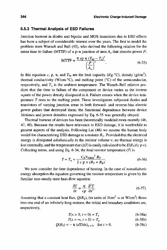
344 Electronic Charge-Induced Damage
6.5.3 Thermal Analysis of ESD Failures
Junction burnout in diodes and bipolar and MOS transistors due to ESD effects has been a subject of considerable interest over the years. The first to model the problem were Wunsch and Bell (45), who derived the following relation for the mean time to failure (MTTF) of a p-n junction of area A^ that absorbs power P:
^vAiir- 2 . (6-35)
In this equation c, p, K, and JM are the heat capacity (J/g-°C), density (g/cm^), thermal conductivity (W/cm-°C), and melting point (°C) of the semiconductor, respectively, and T^ is the ambient temperature. The Wunch-Bell relation pre-dicts that the time to failure of the component or device varies as the inverse square of the power density dissipated in it. Failure ensues when the device tem-perature T rises to the melting point. These investigators subjected diodes and transistors of varying junction areas to both forward- and reverse-bias electric power pulses that destroyed them; the functional dependence between device lifetimes and power densities expressed by Eq. 6-35 was generally obeyed.
Thermal burnout of devices has been theoretically modeled more recently (46, 47, 48). Because the results have relevance to ESD damage, it is worthwhile to present aspects of the analysis. Following Lai (46) we assume the human body model for characterizing ESD damage to a resistor Rj. Provided that the electrical energy is dissipated adiabatically in the resistor volume v, no thermal energy is lost externally, and the temperature rise (AT) is easily calculated to be E{R^)l{c p v). Collecting terms, and using Eq. 6-34, the final resistor temperature (7) is
T=T,^-^^^^i-\-. (6-36) 2 c p V f/?T +/?B)
We now consider the time dependence of heating. In the case of nonadiabatic energy absorption the equation governing the resistor temperature is given by the familiar non-steady-state heat-flow equation
Assuming that a constant heat flux, Q{R^), (in units of J/cm^ -s or W/cm^) flows into one end of an infinitely long resistor, the initial and boundary conditions are, respectively,
T{x > 0, r = 0) = To (6-38a) T{x = oo, r > 0) = To (6-38b)
Q{R^) = - K {dT/dx)^ = 0 for r > 0. (6-38c)
6.5 Electrical Overstress and Electrostatic Discharge 345
The solution to the above boundary value problem is readily obtained using Laplace transforms and is given by
r=r„ + 2Q(RT) - j exp - — V i^'^'V^ (6-39)
where the thermal diffusivity K (cm /s) = K/(cp). Normally we are only interested in the temperature at the resistor surface (x •
0), and therefore, Eq. 6-39 reduces to
r=r..^(fy° = r..2e,Rj t ^1/2 (71 cp K)
Assuming that the heat flux Q(RT) is equal the power density P/AQ,
t -'f) 71 cp K
(6-40)
(6-41)
where A^ is the resistor surface area through which heat flows. Aside from numer-ical constants the result is essentially the Wunsch-Bell relationship (Eq. 6-35) after associating t with MTTF.
The solution of Eq. 6-39 directly applies to square wave testing where the heat flux is constant during pulse duration t. However, in an ESD test, the pulse decays exponentially such that over 99% of the power is dissipated in the first five time constants. An average power, <P> is dissipated for t = 5T, and therefore,
— ^ ^ ) 5T
71 cp K (6-42)
The value of <P> can be readily calculated over this time period through the use of Eq. 6-32
<P> = = T.t[^ exp - (/?T) dt
RTIO [exp (-0) - exp (-10)] -^T^o
A couple of examples will illustrate the use of these equations.
(6-43)
Example 6-1 A pulse of 4500 V is discharged from a person into a p-n junc-tion. The junction area is 5 x 10"^ cm^ and the resistance is 20 Q. Assume that the voltage across the device is negligible compared with that of the ESD pulse. a. Over what time span does the discharge occur? b. What is the maximum current? c. Calculate the power density discharged through the diode.
346 Electronic Charge-lnducecl Pamtge
Answer a. For the human body model the time constant is x = CB (RT + ^B)-Substituting, x ^ 100 x 10" ^ (20 + 1500) = 0.152 |Jis. Therefore, 5T = 0.76 ^s. b. Ohm's law simply states that /« = VHBM/(/^T + RB) = 4500/(20 + 1500) = 2.96 A, c. The power density is <F>/A^, or Rj io^/(10 Ao). Substituting, <P>IA^ = 20
(2.96)^/[10 (5 X 10"^)] = 35 MW/cml
Example 6-2 What human-body voltage pulse is necessary to cause a 1 cm long, 20 i m diameter gold wire to melt under adiabatic conditions? Gold has a melting temperature (I'M) of 1064' C, a density (p) of 19.3 g/cm^, a heat ca-pacity (c) of 0.13 J/g-K, and a resistivity given by 2.4 x [1 + 0.0034(r°C - 20)] (AQ-cm,
Answer According to Eq. 6-36, the human-body voltage is given by VHBM = {(TM - To)[2 c p v(/?w -f RB)yiC^w)]^^, where /?w is the wire resistance. In calculating /?w» it is assumed that the average temperature is 550°C, so that /?w ^ 2.4 x 10~^ [1 + 0.0034(550 - 20)][1/TC (10~^)^] = 2.1 Q. The resistor volume is 3.1 X 10"^ cml Therefore, upon substitution, VHBM = {(550 - 20)[2 x 0.13 x 19,3 X (3.1 X 10"^) (2,1 -h 1500)]/(100 x 10"'" x 2,1)} *'' = 243 kV. Such a large pulse magnitude indicates why wires will not open from human body ESD.
The Wunsch-Bell-like failure model has been extended to both earlier and later times by considering shorter and longer ESD pulse widths as shown in Fig, 6-23. Failure power-density thresholds vary with failure time /fas
100
1 1 O ^ 10 JZ
1 -S 3 U.
1 ' " I
i
" ' ' \
K 3 ^
^
1 J
H
-]
1
.1 10 100
Pulse Width (ins)
1000
Fig. 6-23 Failure threshold power versus pulse width, illustrating three regimes of behavior indicated by Eq. 6-44. From reference 40. Experimental data points are due to H. Domingos, Pwc. EOS / ESD Symp. EOS 2, 6 (1980)
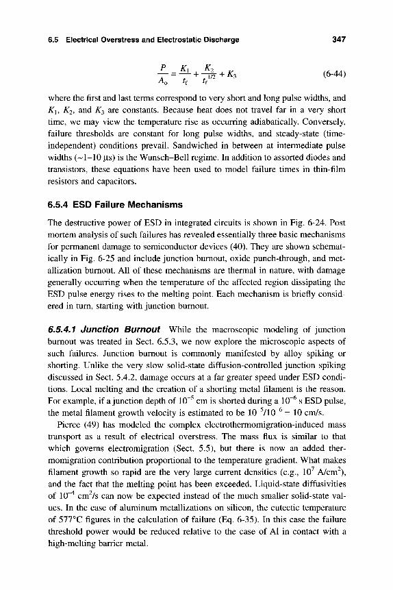
6.5 Electrical Overstress and Electrostatic Discharge 347
f = 7 ' + 7 & + 3 (6-44)
where the first and last terms correspond to very short and long pulse widths, and Ki, K2, and K^ are constants. Because heat does not travel far in a very short time, we may view the temperature rise as occurring adiabatically. Conversely, failure thresholds are constant for long pulse widths, and steady-state (time-independent) conditions prevail. Sandwiched in between at intermediate pulse widths (-'I-IO |is) is the Wunsch-Bell regime. In addition to assorted diodes and transistors, these equations have been used to model failure times in thin-film resistors and capacitors.
6.5.4 ESD Failure Mechanisms
The destructive power of ESD in integrated circuits is shown in Fig. 6-24. Post mortem analysis of such failures has revealed essentially three basic mechanisms for permanent damage to semiconductor devices (40). They are shown schemat-ically in Fig. 6-25 and include junction burnout, oxide punch-through, and met-allization burnout. All of these mechanisms are thermal in nature, with damage generally occurring when the temperature of the affected region dissipating the ESD pulse energy rises to the melting point. Each mechanism is briefly consid-ered in turn, starting with junction burnout.
6.5.4.1 Junction Burnout While the macroscopic modeling of junction burnout was treated in Sect. 6.5.3, we now explore the microscopic aspects of such failures. Junction burnout is commonly manifested by alloy spiking or shorting. Unlike the very slow solid-state diffusion-controlled junction spiking discussed in Sect. 5.4.2, damage occurs at a far greater speed under ESD condi-tions. Local melting and the creation of a shorting metal filament is the reason. For example, if a junction depth of 10"^ cm is shorted during a 10"^ s ESD pulse, the metal filament growth velocity is estimated to be 10"^/10"^ =10 cm/s.
Pierce (49) has modeled the complex electrothermomigration-induced mass transport as a result of electrical overstress. The mass flux is similar to that which governs electromigration (Sect. 5.5), but there is now an added ther-momigration contribution proportional to the temperature gradient. What makes filament growth so rapid are the very large current densities (e.g., 10^ A/cm^), and the fact that the melting point has been exceeded. Liquid-state diffusivities of 10"^ cm^/s can now be expected instead of the much smaller solid-state val-ues. In the case of aluminum metallizations on silicon, the eutectic temperature of 577°C figures in the calculation of failure (Eq. 6-35). In this case the failure threshold power would be reduced relative to the case of Al in contact with a high-melting barrier metal.
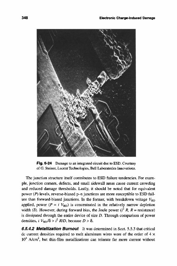
348 Electronic Charge-Induced Damage
Fig. 6-24 Damage to an integrated circuit due to ESD. Courtesy of G. Steiner, Lucent Technologies, Bell Laboratories Innovations.
The junction structure itself contributes to ESD failure tendencies. For exam-ple, junction comers, defects, and small sidewall areas cause current crowding and reduced damage thresholds. Lastly, it should be noted that for equivalent power (P) levels, reverse-biased p-n junctions are more susceptible to ESD fail-ure than forward-biased junctions. In the former, with breakdown voltage VBD applied, power (P = / VBD) is concentrated in the relatively narrow depletion width (5). However, during forward bias, the Joule power (/ R, R = resistance) is dissipated through the entire device of size D. Through comparison of power densities, / VBD/S > f' RID, because D> 5.
6.5.4.2 Metallization Burnout It was determined in Sect. 5.5.3 that critical dc current densities required to melt aluminum wires were of the order of 4 x 10"* A/cm^, but thin-film metallizations can tolerate far more current without
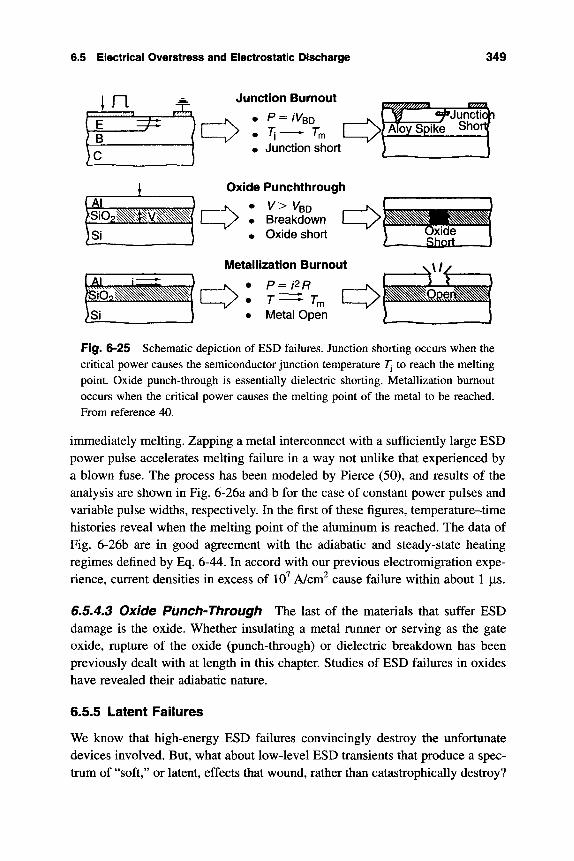
6.5 Electrical Overstress and Electrostatic Discharge 349
in TTrl,
B
Junction Burnout • P = /VBD
sss\ Junction
/ [ Z > . 7 ] - ^ 7 , lH^AToySpike Shoj ' J ' n r i
Junction short
Oxide Punchthrough
[ Z l ) > • Breakdown [ I I ^ > ^ ^ ^ H I I i ^ ^ S • Oxide short \ ^Y\^e I
Metafiization Burnout P = /2R
Metal Open
Fig. 6-25 Schematic depiction of ESD failures. Junction shorting occurs when the critical power causes the semiconductor junction temperature Tj to reach the melting point. Oxide punch-through is essentially dielectric shorting. Metallization burnout occurs when the critical power causes the melting point of the metal to be reached. From reference 40.
immediately melting. Zapping a metal interconnect with a sufficiently large ESD power pulse accelerates melting failure in a way not unlike that experienced by a blown fuse. The process has been modeled by Pierce (50), and results of the analysis are shown in Fig. 6-26a and b for the case of constant power pulses and variable pulse widths, respectively. In the first of these figures, temperature-time histories reveal when the melting point of the aluminum is reached. The data of Fig. 6-26b are in good agreement with the adiabatic and steady-state heating regimes defined by Eq. 6-44. In accord with our previous electromigration expe-rience, current densities in excess of 10^ A/cm^ cause failure within about 1 i is.
6.5.4.3 Oxide Punch-Through The last of the materials that suffer ESP damage is the oxide. Whether insulating a metal runner or serving as the gate oxide, rupture of the oxide (punch-through) or dielectric breakdown has been previously dealt with at length in this chapter. Studies of ESD failures in oxides have revealed their adiabatic nature.
6.5.5 Latent Failures
We know that high-energy ESD failures convincingly destroy the unfortunate devices involved. But, what about low-level ESD transients that produce a spec-trum of "soft," or latent, effects that wound, rather than catastrophically destroy?
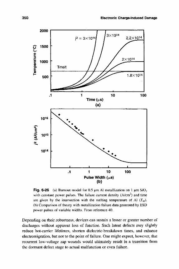
350 Electronic Charge-Induced Damage
2000
S 1500
o
0)
S 1000 0) Q. E o
500
Tmelt
j2 = 3X10¹⁴/
1
y / 2X10¹⁴
^/^.^"^ 1.8X10¹⁴|
1 1 1 10
Time (|xs)
(a)
100
1016
E 5 1015 < CM ••*^
1014
N^« •
x%. N %
..-.,.,1...... . -
^ •
1. . -., i \ 1 1 10
Pulse Width (fjis) (b)
100
Fig. 6-26 (a) Burnout model for 0.5 |Lim Al metallization on 1 jiun Si02 with constant power pulses. The failure current density (A/cm ) and time are given by the intersection with the melting temperature of Al (I'M).
(b) Comparison of theory with metallization failure data generated by ESD power pulses of variable widths. From reference 40.
Depending on their robustness, devices can sustain a lesser or greater number of discharges without apparent loss of function. Such latent defects may slightly reduce hot-carrier lifetimes, shorten dielectric-breakdown times, and enhance electromigration, but not to the point of failure. One might expect, however, that recurrent low-voltage zap wounds would ultimately result in a transition from the dormant defect stage to actual malfunction or even failure.
6.5 Electrical Overstress and Electrostatic Discharge 351
A summary of the results of latency testing reveals that
1. Life-test studies yield inconclusive results. 2. Most devices degraded by BSD actually improve or heal during life testing. 3. Many latent failures are simply leaky pins operating within specifications. 4. Gate oxides are probably prone to latent defects. 5. On-chip protection structures are generally such that further degradation is
unlikely during normal device operation.
On the basis of this collection of observations, latent damage and failure is dif-ficult to model with any certainty; its impact on reliability is likewise uncertain.
6.5.6 Guarding Against ESD
Two basic strategies are employed to protect sensitive electronics from ESD damage, namely, preventing it from occurring and modifying devices and cir-cuits to make them immune (4, 43, 51). The first approach deals with sources of charge and voltage external to the electrical hardware, and attempts to neutralize potential harmful effects arising from personnel, work stations, packaging and transportation, and the workplace environment. For example, by wearing metal wrist straps, antistatic gloves and smocks, ESD damage from handling can be minimized. Equipping workbenches with tabletops and mats that dissipate charge, and using grounded tools (e.g., soldering iron tips, solder suckers), stools, and chairs helps to insure against ESD damage at workstations. Similarly, the use of grounded carts, antistatic bags and tote boxes, as well as shielded or protective containers for transporting IC chips, minimizes damage arising during movement of electronic products. Lastly, the work environment can be made safer through humidity control and suppressing ionization of air.
It is virtually impossible to eliminate ESD from occurring, so the second, and most widely used, strategy is to improve device immunity to destructive dam-age. One way to do this is to connect solid-state clamping elements between critical points such as the input and ground of devices. If the ESD-induced volt-age exceeds the clamping voltage, the element turns on and becomes a low-impedance shunt to divert currents to ground. Incorporation of either shunt capacitors or series inductor filters are other approaches to minimizing ESD damage. Further discussion of circuits to protect electronics against ESD is well beyond the scope of this book.
6.5.7 Some Common IVIyths About ESD
Common to all poorly understood damage phenomena is an accumulated "wis-dom" invested with differing proportions of fact and fiction. Sometimes this wis-dom is scientifically based, but in other cases it may be little more than a collection
352 Electronic Charge^nduced Damage
of myths. Because the subject of BSD has its share of them, it is jmident to be aware of the mythology before proceeding to devise countermeasures. McAteer (43) has enumerated the following myths about static electricity and BSD.
1. Conductive components are never involved in ESD. 2. Antistatic materials always protect components that are susceptible to static
electricity. 3. ESD is primarily an MOS problem. 4. Devices with input-protection circuitry are always immune to ESD. 5. Components are insensitive to ESD after they are installed in an assembly. 6. Devices or printed-circuit boards with connector pins shorted together are
immune to ESD. 7. Antistatic, static-dissipative, and conductive materials are equivalent. 8. ESD damage to printed-circuit boards can be prevented by handling them by
the edges. 9. Controlling the relative humidity to greater than 40% eliminates static prob-
lems. 10. Static-electricity problems can be eliminated by controlling room ionization.
Clearly, separating fact from fiction, evaluating myths, and successfully com-bating ESD will necessitate a more advanced understanding of the complex interaction among electrostatics, materials, and circuit analysis. If this is not achieved, one myth that will persist is. We're not having ESD problems.
EXERCISES
6-1 Large, conically shaped ceramic insulators with a fluted-surface profile are often used to isolate high electric potentials from ground in high-voltage transmission lines. Give a reason for the wavy profile in these insulators.
6-2 Capacitors composed of 11 nm thick Si02 gates sandwiched between p-type Si substrates and polysilicon were stressed to breakdown either through application of a constant current of 40 jLiAor a constant voltage bias of 12.866 V. For electrode areas measuring 0.02 mm^, 50% of the capacitors failed at a breakdown charge of QBD = 2 C /cm^, independent of testing method. a. What is the mean time to failure based on constant-current testing? b. Can the resistivity of the oxide be calculated from this information? If
so, how does the apparent value compare with typical resistivities of Si02?
Exercises 353
6-3 The gate oxide of an MOS transistor has an area of 1 |im^ and it is effec-tively connected to a square metal antenna with an area of 1200 |i.m , as shown in Fig. 6-14. a. During a plasma-etching step a current density of 10 mA/cm^ is sus-
tained. What current is supplied to the oxide? b. Suppose a nonconducting mask 0.2 |Lim thick sits above the metal
antenna so that only the antenna film edges are exposed to the plasma. How much current is supplied to the gate now?
6-4 At the instant of dielectric breakdown, the discharge current density is much larger than typically applied external densities resulting from cur-rents of microamps. Demonstrate this fact by assuming that the discharge current arises from flow of displacement charge in '-O.l jLis. Note that the electric displacement D(q) and field (S') are related by D(q) = EEOS", where e is the dielectric constant and 8o is the permittivity of free space. The elec-trode area is 0.01 mm^, and the discharge damage area is 1 |im^.
6-5 Based on the results of the previous problem calculate a. the total energy density at breakdown for a capacitor of unit area and
thickness, and estimate b. the radius of the breakdown crater of melted material assuming it is
either Si or Si02. How does the estimated value compare to the actual crater size? Assume that the average heat capacities of Si and Si02 are 6 and 14.5 cal/mol-K, respectively.
6-6 A 10 nm thick gate oxide suffers dielectric breakdown at an electric field of 10 MV/cm. It was observed that a 100 nm diameter pinhole formed within 0.12 ms. What current was probably responsible for breakdown if the Si02 melted? Assume that the melting point of Si02 is 1700°C.
6-7 Gate oxides are now approximately 8 nm or less in thickness. Speculate what happens to the distribution and magnitude of the ionic, oxide trapped, fixed, and interfacial oxide charge. In particular, comment on the magni-tudes of the electrostatic interactions between these charge distributions.
6-8 It has been found that TDDB failure times of Si02 capacitors remain rela-tively independent of oxide thickness when polySi contacts are used. How-ever, for Al contacts the failure times decrease greatly in thinner oxides. Why?
6-9 It is desired that a 12.5 nm thick dielectric last 5 years within a capacitor charged to 5 volts. What breakdown electric field would be probably be measured if the voltage were ramped at a rate of 1 V/m?
354 Electronic Charge-Induced Damage
6-10 Time-dependent dielectric breakdown failure times are commonly plotted as log MTTF vs l/cf rather than log [(MTTF)S'^] vs l/cT. a. Why is this latter way of plotting data more physically appealing? b. At high fields, does a plot of log MTTF vs l/(f over- or underestimate
the time to failure if log [(MTTF) <f ] vs US' is the correct dependence? c. Set up equations that would enable the correspondence between volt-
age-ramping and constant-voltage tests to be determined assuming MTTF « l/S^ exp (l/S).
6-11 Ultrathin oxides grown on silicon wafers having longer carrier lifetimes are observed to be more reliable (as measured by injected charge to break-down) than oxides grown on wafers with shorter carrier lifetimes. Give a plausible reason for this finding.
6-12 It has been suggested (W. B. Henley et ai, 31st Annual Proceedings of the IEEE Reliability Physics Symposium, p. 22 (1993)) that iron-precipitate contaminants of size d (cm) increase the effective local electric field in Si02 linearly according to c eff = iVJ^o) (1 + 7 x 10^ d), where V^ is the applied voltage and X^ is the oxide thickness. What failure time can be expected in 10 nm thick oxides containing 0.5 nm precipitates? How does this compare to the MTTF when precipitates are 2 nm in size? Assume ^OR = 10' ^ s and GR = 320 MV/cm.
6-13 Dielectric breakdown in mica capacitors appears to be govemed by ion transport. Suggest a relationship between the failure time, material con-stants, temperature, and applied electric field.
6-14 Estimate the largest leakage current a gate oxide measuring 0.1 |Lim can tolerate if it must survive for 5 years if QBD is 10 C/cm^.
6-15 a. Derive a single comprehensive equation for the mean time to failure of Si02 films as a function of applied electric field, temperature, and thick-ness, if the oxide properties are as depicted in Figs. 6-12 and 6-13.
b. What testing temperature was used to obtain the data shown in Fig. 6-12?
6-16 a. If the quantity m in Eq. 6-28 is changed by an amount dm, by what fac-tor does the mean lifetime of a MOSFET subject to hot-electron damage change?
b. What is the apparent activation energy for hot-electron degradation in devices whose behavior is shown in Fig. 6-20c?
6-17 a. Mention three strategies to limit hot-electron damage in field effect tran-sistors.
References 355
b. Annealing devices in deuterium instead of hydrogen appears to reduce hot-electron degradation. Suggest a possible reason why.
6-18 Provide physical arguments for the following observations: a. Breakdown of dielectrics has similarities to the plastic deformation of
metals. b. Dielectric breakdown can be caused by either electron or hole injection
processes. c. Electronic components subjected to narrow voltage-pulse widths can
sustain higher power levels prior to failure. d. Hot electrons can reach temperatures of tens of thousands of degrees.
6-19 Consider a discrete silicon diode whose p-n junction area is 1 |im^. An electric power pulse destroyed the device in 10 ns. Roughly estimate the threshold power discharged in the diode.
6-20 The lateral extent of the heat-induced discoloration surrounding a failure site has been used as a means of crudely estimating the time duration of an EOS event. Assume that the temperature in the damage zone is given by T =Tyi Erfc ^^fj , and the discoloration zone extends to points where tem-peratures of \ TM are reached.
In a certain IC chip failure, silicon was discolored for a distance of ' 5 |im. What pulse time is suggested? What is the reason for the appearance of colors in thermally damaged silicon?
6-21 Sketch the critical power density versus pulse time behavior for GaAs devices as in Fig. 6-23. Are GaAs devices more or less sensitive to ESD than Si devices? Note for GaAs: p = 5.32 g/cm^ TM = 1236°C, K = 0.81 W/cm-°C, Cp = 0.35 J/g-°C.
REFERENCES
1. S. M. Sze, Physics of Semiconductor Devices, 2nd Ed., Wiley, New York (1981).
2. J. S. Suehle, P. Chaparala, C. Messick, W. M. Miller, and K. C. Boyko, 32nd Annual Proceedings of the IEEE Reliability Physics Symposium, p. 120 (1994).
3. R. B. Comizzoli, in Materials Developments in Microelectronic Packaging: Performance and Reliability, ed. P. J. Singh, ASM, 311 (1991).
356 Electronic Charge-Induced Damage
4. Y. Leblebici and S. M. Kang, Hot Carrier Reliability ofMOS VLSI Circuits, Kluwer, Boston (1993).
5. S. M. Sze, Semiconductor Devices—Physics and Technology, Wiley, New York (1985).
6. D. M. Fleetwood, IEEE Trans, on Nuclear Science, NS-39, 269 (1992). 7. D. R. Wolters and J. J. Van der Schoot, Philips J. Res. 40, 115 (1985). 8. D. R. Wolters and J. J. Van der Schoot, Philips J. Res. 40, 164 (1985). 9. R. S. Scott, N. A. Dumin, T. W. Hughes, and D. J. Dumin, 33rd Annual Pro-
ceedings of the IEEE Reliability Physics Symposium, p. 131 (1995). 10. J. S. Suehle, B. W. Langley, and C. Messick, Tutorial Notes, IEEE Interna-
tional Reliability Physics Symposium, 6.1 (1995). 11. J. Lee, I-C Chen, and C. Hu, 26th Annual Proceedings of the IEEE Relia-
bility Physics Symposium, p. 131 (1988). 12. R. Moazzami, J. C. Lee, and C. Hu, IEEE Trans, on Electron Devices 36,
2462 (1989). 13. J. F. Verweij and J. H. Klootwijk, Microelectronics J. 27, 611 (1996). 14. T. Ohmi, K. Nakamura, and K. Makihara, 32nd Annual Proceedings of the
IEEE Reliability Physics Symposium, p. 161, (1994). 15. T. Ohmi, Proc. IEEE 81(5),716 (1993). 16. J. W. McPherson and D. A. Baglee, 23rd Annual Proceedings of the IEEE
Reliability Physics Symposium, p. 1 (1985). 17. E. S. AnoUck and G. R. Nelson, IEEE Trans, on Reliability, R-29,217 (1980). 18. A. G. Sabnis, VLSI Reliability, VLSI Electronics Microstructure Science,
Vol. 22, Academic Press, San Diego (1990). 19. D. R. Wolters, Philips Tech Rev. 43, 330 (1987). 20. D. J. Dumin, Tutorial Notes, IEEE International Reliability Physics Sympo-
sium, 2.1 (1995). 21. R. Degraeve, J. L. Ogier, R. Bellens, Ph. Roussel, G. Groesseneken, and
H. E. Maes, 34th Annual Proceedings of the IEEE Reliability Physics Sym-posium, p. 44 (1996).
22. C. K. Chan, IEEE Trans, on Reliability 39, 147 (1990). 23. J. C. Chen, S. Holland, and C. Hu, 23rd Annual Proceedings of the IEEE
Reliability Physics Symposium, p. 24 (1985). 24. A. Berman, 19th Annual Proceedings of the IEEE Reliability Physics Sym-
posium, p. 204 (1981). 25. R. Moazzami and C. Hu, Tutorial Notes, IEEE International Reliability
Physics Symposium, 5.1(1992). 26. K. P. Cheung, Tutorial Notes, IEEE International Reliability Physics Sym-
posium, 4.1 (1997). 27. Y. Uraoka, K. Eriguchi, T. Tamaki, and K. Tsuji, IEEE Trans, on Semicon-
ductor Manufacturing 7(3), 293 (1994).
References 357
28. T. Miyashita, Proceedings lEEE-NEMA Electrical Insulation Conference, Boston, 131 (1969).
29. J. J. Xu and S. A. Boggs, IEEE Electrical Insulation Mag. 10 (5), 29 (1994). 30. K. Mistry and B. Doyle, IEEE Circuits and Devices, 11, 33 (1995). 31. E. Takeda, Tutorial Notes, IEEE International Reliability Physics Sympo-
sium, Ibl (1993). 32. C. Hu, S. C. Tarn, F.-C. Hsu, P. K. Ko, T. Chan, and K. W. Terrill, IEEE
Trans, on Electron Devices, ED-32, 375 (1985). 33. S. Tarn, P. K. Ko and C. Hu, IEEE Trans, on Electron Devices, ED-31, 1116
(1984) 34. W. Weber, M. Brox, T. Kuenemund, H. M. Muehlhoff, and D. Schmitt-
Landsiedel, IEEE Trans, on Electron Devices, ED-38, 1859 (1991). 35. W. Weber and M. Brox, MRS Bulletin, XVIII (12), 36 (1993). 36. R. Bellens, P. Heremans, G. Grosseneken, and H. E. Maes, 26th Annual Pro-
ceedings of the IEEE Reliability Physics Symposium, p. 8, (1988). 37. H. E. Maes, P. Heremans, R. Bellens, and G. Grosseneken, Quality and Reli-
ability Engineering International 7, 307 (1991). 38. J. Scarpulla, J. Dunkley, S. Lemke, E. Sabin, and M. Young, 35th Annual
Proceedings of the IEEE Reliability Physics Symposium, p. 34, (1997). 39. C. Tedesco, C. Canali, F. Magistral!, A. Paccagnella, and E. Zanoni, Quality
and Reliability Engineering International 9, 371 (1993). 40. D. G. Pierce, Tutorial Notes, IEEE International Reliability Physics Sympo-
sium, 8.1 (1995). 41. N. Sclater, Electrostatic Discharge Protection for Electronics, TAB Books,
McGraw Hill, Blue Ridge Summit, PA (1990). 42. A. Amerasekera and J. Verwey, Quality and Reliability Engineering Inter-
national 8, 259 (1992). 43. O. J. McAteer, Electrostatic Discharge Control, McGraw Hill (1990) 44. W. D. Greason, Electrostatic Discharge in Electronics, Research Studies
Press, Wiley, New York (1992) 45. D. C. Wunsch and R. R. Bell, IEEE Trans, on Nuclear Science 15, 244
(1968) 46. T. T. Lai, IEEE Trans, on Components, Hybrids and Manuf. Tech. 12, 627
(1989). 47. V. M. Dwyer, A. J. Franklin, and D. S. Campbell, IEEE Trans, on Electron
Devices 37, 2381 (1990) 48. H. H. Choi and T. DeMassa, Solid State Electronics 36, 1511 (1993). 49. D. G. Pierce, Proc. EOS/ESD Symp. EOS 7, 67 (1985). 50. D. G. Pierce, Proc. EOS/ESD Symp. EOS 4, 55 (1982). 51. W. Boxleitner, IEEE Spectrum 26 (8), 36 (1989).

This Page Intentionally Left Blank
Chapter 7
Environmental Damage to Electronic Products
7.1 INTRODUCTION
The sources of IC damage considered up to this point originated within the mate-rials and substances used in manufacturing. But now we confront degradation and damage to electronic products from outside sources such as humid atmos-pheres, airborne contaminant particles, and ionizing radiation. Even in the very early years of microelectronics it was already recognized that moisture and atmospheric particulates, often ionic in nature, posed serious reliability problems in devices, components, and packages. Thin-film metallizations and fine wires composed of corrodible metals (e.g., Al, Ag) and insulation (plastic, ceramics) prone to moisture absorption, resulted in degradation products that were uncom-fortably large in size compared to the small feature dimensions involved. Today, humidity-induced corrosion of exposed or unprotected metals and water pickup, as well as release from polymers, are among the major failure mechanisms in electronic products.
In this chapter we explore a number of issues related to environmental damage starting with the sources of atmospheric contamination. Then the kinetics of per-meation as well as leakage of harmful environmental gases (e.g., water vapor) and contaminants into electronic packages will be discussed. Later we shall see how particulates and humid environments act in synergy to promote corrosion and metal migration damage.
359
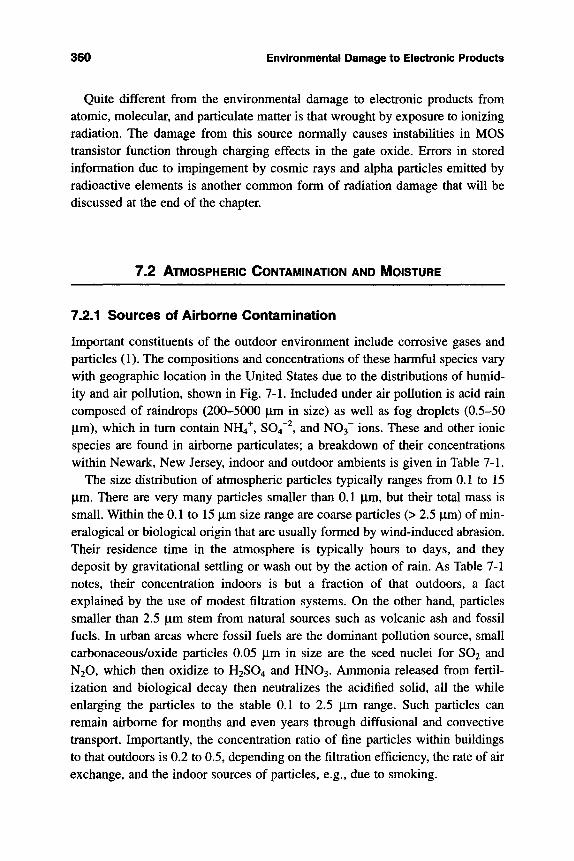
360 Environmental Damage to Electronic Products
Quite different from the environmental damage to electronic products from atomic, molecular, and particulate matter is that wrought by exposure to ionizing radiation. The damage from this source normally causes instabilities in MOS transistor function through charging effects in the gate oxide. Errors in stored information due to impingement by cosmic rays and alpha particles emitted by radioactive elements is another conmion form of radiation damage that will be discussed at the end of the chapter.
7.2 ATMOSPHERIC CONTAMINATION AND MOISTURE
7.2.1 Sources of Airborne Contamination
Important constituents of the outdoor environment include corrosive gases and particles (1). The compositions and concentrations of these harmful species vary with geographic location in the United States due to the distributions of humid-ity and air pollution, shown in Fig. 7-1. Included under air pollution is acid rain composed of raindrops (200-5000 |im in size) as well as fog droplets (0.5-50 |Lim), which in turn contain N H / , S04~^, and NOs" ions. These and other ionic species are found in airborne particulates; a breakdown of their concentrations within Newark, New Jersey, indoor and outdoor ambients is given in Table 7-1.
The size distribution of atmospheric particles typically ranges from 0.1 to 15 |Lim. There are very many particles smaller than 0.1 |im, but their total mass is small. Within the 0.1 to 15 |Lim size range are coarse particles (> 2.5 p.m) of min-eralogical or biological origin that are usually formed by wind-induced abrasion. Their residence time in the atmosphere is typically hours to days, and they deposit by gravitational settling or wash out by the action of rain. As Table 7-1 notes, their concentration indoors is but a fraction of that outdoors, a fact explained by the use of modest filtration systems. On the other hand, particles smaller than 2.5 |im stem from natural sources such as volcanic ash and fossil fuels. In urban areas where fossil fuels are the dominant pollution source, small carbonaceous/oxide particles 0.05 |im in size are the seed nuclei for SO2 and N2O, which then oxidize to H2SO4 and HNO3. Anmionia released from fertil-ization and biological decay then neutralizes the acidified solid, all the while enlarging the particles to the stable 0.1 to 2.5 |Lim range. Such particles can remain airborne for months and even years through diffusional and convective transport. Importantly, the concentration ratio of fine particles within buildings to that outdoors is 0.2 to 0.5, depending on the filtration efficiency, the rate of air exchange, and the indoor sources of particles, e.g., due to smoking.
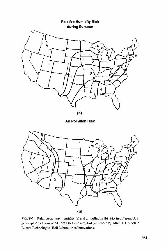
Relative Humidity Risic during Summer
(a)
Air Pollution Risk
(b)
Fig. 7-1 Relative summer humidity (a) and air pollution (b) risks in different U. S. geographic locations rated from 1 (least severe) to 4 (most severe). After D. J. Sinclair, Lucent Technologies, Bell Laboratories Innovations.
361
362 Environmental Damage to Electronic Products
Table 7-1 Average Concentrations of Ionic Species and Corrosive Gases in the Air Around Newark, NJ (ng/m^)
Particles
cr so/-Na-" N H / K^ Mg^^ Ca^^ TOTAL MASS
Fine 4
721 14
168 19 2
10 2880
Indoor
Coarse 4
25 3 0 2 1
20 6100
Outdoor
Fine 66
5,213 103
1,631 53 14 25
18,090
Coarse 502 725 446
1 30 90
297 12,340
Gases
Sulfur dioxide Nitrogen oxides Chlorine gases Reduced sulfur Ammonia
5,400 24,000
510 800
40,000
From R. B. Comizzoli, R. R Frankenthal, R. E. Lobnig, G. A. Peins, L. A. Psota-Kelty, D. J. Siconolfi, and D. J. Sinclair, The Electrochem. Soc. Interface 26, Fall (1993).
The particulate and gaseous contaminants that manage to bypass filtration bar-riers in buildings land on the vertical and horizontal surfaces of electronic com-ponents and systems, where they have the potential to cause corrosion. In wafer fabrication facilities some finer particles even penetrate clean-room defenses and become the defects that lower yields.
It is instructive to predict the surface accumulation rate (A) of a given pollu-tant particle assuming the known outdoor concentration (Q) and filtration effi-ciency (F). Filters are rated in terms of the ratio of contaminant level indoors (Ci) after passing through the filter, to the outdoor level; i.e., (F = CJCQ). Typi-cally CJCQ = 0.1 for high-efficiency filters. An additional quantity that must be known is the particle terminal settling, or deposition, velocity, v, (Eq. 3-13). We now simply note that the accumulation rate is the product of the indoor concen-tration and deposition velocity, and in typical units
A (|ig/cm^-yr) = 0.526 C, (ixgW) v(cm/s). (7-1)
As an example consider the accumulation of S04^~ for which Q = 20 |ig/m^. In passing through a filter for which CJCQ = 0.12, and assuming v = 0.005 cm/s, substitution yields a surface accumulation of 6.31 x 10"^ |Lig/cm -yr. Measure-
7.2 Atmospheric Contamination and l\/loisture 363
ments in many cities across the U.S. typically reveal that annual sulfate and chloride accumulations on outdoor zinc and aluminum surfaces range between 0.1 to 0.8 |Lig/cml
7.2.2 Moisture Damage
Moisture-induced damage (e.g., swelling of IC packages, electrical shorting) and corrosion of metal components (e.g., conductors, contacts) and auxiliary hard-ware (e.g., closed-loop laser cooling system (2)) associated with electrical and electronic equipment have traditionally been major reliability concerns. An annual monetary toll of a few billion dollars is not an exaggeration of the mag-nitude of moisture/corrosion problems in electrical equipment. Although our focus later will be corrosion in microelectronics, larger electrical and electronic systems are also quite vulnerable (3). Similarly, a review of corrosion damage in disk-recorder heads, aircraft avionic equipment, stepping motors, klystron tubes and other microwave equipment, printed wiring boards, antennas, contacts, and so on, can be found in reference 4. Since a necessary condition for corrosion is the presence of water, we start by exploring aspects of moisture accumulation on surfaces and permeation of electronic packages (5, 6).
7.2.2.1 Moisture Accumulation on Surfaces According to the kinetic theory of gases, a surface immersed in an environment containing a gas at pres-sure P will be impacted by a flux (O) of its molecules given by
(27C MRT)^^^
or
O = —^ i72— (molecules/cm^-s). (7-2)
In these expressions M is the molecular weight, the pressure is expressed in mm Hg or torr (1 torr = 1mm Hg = 133.3 Pa), and RThsis the usual meaning. Before this formula is used, let us consider relative humidity (RH), which is defined as the ratio of the actual pressure of water vapor to the equilibrium vapor pressure at the given temperature. For water at 25°C the equilibrium vapor pressure is 24 torr; if, for example, RH = 42%, the value of P is 0.42 x 24, or 10 torr. Substi-tution in Eq. 7-2 yields a flux of 4.8 x 10 ^ H2O molecules/cm^-s at this temper-ature. Since a solid surface contains some 10^^ atomic sites per cm^, a monolayer of condensed water will form in approximately 0.2 |xs, assuming that all imping-ing vapor molecules stick.
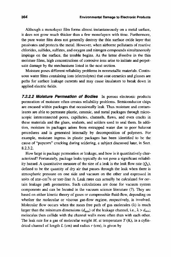
364 Environmental Damage to Electronic Products
Although a monolayer film forms almost instantaneously on a metal surface, it does not grow much thicker than a few monolayers with time. Furthermore, the pure water film does not generally destroy the thin surface oxide layer that passivates and protects the metal. However, when airborne pollutants of reactive chlorides, sulfides, sulfates, and oxygen and nitrogen compounds simultaneously impinge on the surface, the trouble begins. As the latter dissolve in the thin moisture films, high concentrations of corrosive ions arise to initiate and perpet-uate damage by the mechanisms listed in the next section.
Moisture poses different reliability problems in nonmetallic materials. Contin-uous water films containing ions (electrolytes) that coat ceramics and glasses are paths for surface leakage currents and may cause insulators to break down in applied electric fields.
7.2.2.2 Moisture Permeation of Bodies In porous electronic products permeation of moisture often creates reliability problems. Semiconductor chips are encased within packages that occasionally leak. Thus moisture and contam-inants are able to permeate plastic, ceramic, and metal packages through micro-scopic interconnected pores, capillaries, channels, flaws, and even cracks in these materials and the glues, sealants, and solders used to seal them. In addi-tion, moisture in packages arises from entrapped water due to poor bakeout procedures and is generated internally by decomposition of polymers. For example, moisture ingress in plastic packages has been identified to be the cause of "popcorn" cracking during soldering, a subject discussed later, in Sect. 8.2.3.2.
How large is package permeation or leakage, and how is it quantitatively char-acterized? Fortunately, package leaks typically do not pose a significant reliabil-ity hazard. A quantitative measure of the size of a leak is the leak flow rate (j2s)» defined to be the quantity of dry air that passes through the leak when there is atmospheric pressure on one side and vacuum on the other and expressed in units of atm-cmVs or torr-liter /s. Leak rates can actually be calculated for cer-tain leakage path geometries. Such calculations are done for vacuum system components and can be located in the vacuum science literature (7). They are based on either kinetic theory of gases or compressible fluid-flow, depending on whether the molecular or viscous gas-flow regime, respectively, is involved. Molecular flow occurs when the mean free path of gas molecules (X) is much larger than the minimum dimensions ( min) of the leakage channel, i.e., X > d^^^', molecules then collide with the channel walls more often than with each other. The leak rate for a gas of molecular weight M, at temperature T (K), in a cylin-drical channel of length L (cm) and radius r (cm), is given by
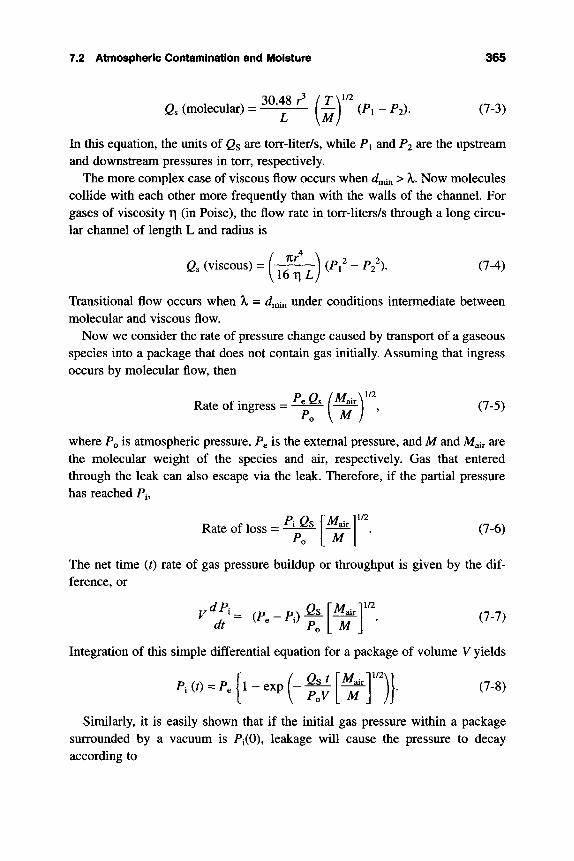
7.2 Atmospheric Contamination and Moisture 365
a (molecular) = ^^'^^ f-^J (Pi - P2). (7-3)
In this equation, the units of Qs are torr-liter/s, while Pi and P2 are the upstream and downstream pressures in torr, respectively.
The more complex case of viscous flow occurs when c?min > X,. Now molecules collide with each other more frequently than with the walls of the channel. For gases of viscosity r\ (in Poise), the flow rate in torr-liters/s through a long circu-lar channel of length L and radius is
Gs (viscous) = ( T ^ ) (^1' - ^2'). (7-4)
Transitional flow occurs when X = Jmin under conditions intermediate between molecular and viscous flow.
Now we consider the rate of pressure change caused by transport of a gaseous species into a package that does not contain gas initially. Assuming that ingress occurs by molecular flow, then
Rate of ingress = ^ ^ ^ ^ y ' ' , (7-5)
where P^ is atmospheric pressure, Pg is the external pressure, and M and Mair are the molecular weight of the species and air, respectively. Gas that entered through the leak can also escape via the leak. Therefore, if the partial pressure has reached Pi,
Rate of loss = ^ ^ ^ \^^T\ (7-6) Po [ M J
The net time (0 rate of gas pressure buildup or throughput is given by the dif-ference, or
1/2
<:'- <-•-•> t [ ^ r Integration of this simple differential equation for a package of volume V yields
Pi(t) = P. n'tn l - e x p ( - ^ | ^ | )}. (7-8)
Similarly, it is easily shown that if the initial gas pressure within a package surrounded by a vacuum is Pi(0), leakage will cause the pressure to decay according to
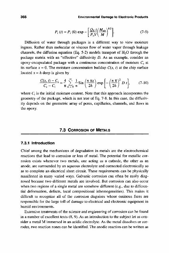
366 Environmental Damage to Electronic Products
Pi (0 = Pi (0) exp [PoVK M
MX (7-9)
Diffusion of water through packages is a different way to view moisture ingress. Rather than molecular or viscous flow of water vapor through leakage channels, the diffusion equation (Eq. 5-2) models transport of H2O through the package matrix with an "effective" diffusivity D. As an example, consider an epoxy-encapsulated package with a continuous concentration of moisture Q at its surface JC = 0. The moisture concentration buildup C(JC, t) at the chip surface located x = h deep is given by
where Q is the initial moisture content. Note that this approach incorporates the geometry of the package, which is not true of Eq. 7-8. In this case, the diffusiv-ity depends on the geometric array of pores, capillaries, channels, and flaws in the epoxy.
7.3 CORROSION OF METALS
7.3.1 Introduction
Chief among the mechanisms of degradation in metals are the electrochemical reactions that lead to corrosion or loss of metal. The potential for metallic cor-rosion exists whenever two metals, one acting as a cathode, the other as an anode, are surrounded by an aqueous electrolyte and connected electronically so as to complete an electrical short circuit. These requirements can be physically manifested in many varied ways. Galvanic corrosion can often be easily diag-nosed because two different metals are involved. But corrosion can also occur when two regions of a single metal are somehow different (e.g., due to differen-tial deformation, defects, local compositional inhomogeneities). This makes it difficult to recognize all of the corrosion disguises whose ominous faces are responsible for the large toll of damage to electrical and electronic equipment in humid environments.
Extensive treatments of the science and engineering of corrosion can be found in a number of excellent texts (8, 9). As an introduction to the subject let us con-sider a metal M immersed in an acidic electrolyte. As the metal dissolves or cor-rodes, two reaction zones can be identified. The anodic reaction can be written as
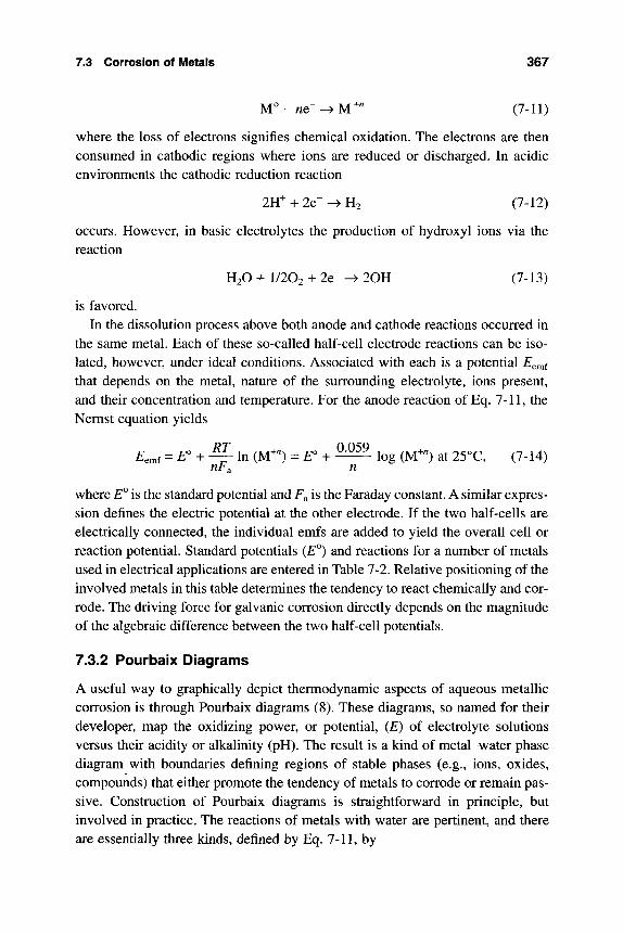
7.3 Corrosion of Metals 367
M ^ - « e " - ^ M " ' " (7-11)
where the loss of electrons signifies chemical oxidation. The electrons are then consumed in cathodic regions where ions are reduced or discharged. In acidic environments the cathodic reduction reaction
2H"' + 2e-->H2 (7-12)
occurs. However, in basic electrolytes the production of hydroxyl ions via the reaction
H2O + I/2O2 + 2e" -^ 20H" (7-13)
is favored. In the dissolution process above both anode and cathode reactions occurred in
the same metal. Each of these so-called half-cell electrode reactions can be iso-lated, however, under ideal conditions. Associated with each is a potential £ emf that depends on the metal, nature of the surrounding electrolyte, ions present, and their concentration and temperature. For the anode reaction of Eq. 7-11, the Nemst equation yields
£emf = £° + ^^^ In (M^") = E° + ^"^^^ log (M-"") at 25°C, (7-14) nF^ n
where E^ is the standard potential and Fa is the Faraday constant. A similar expres-sion defines the electric potential at the other electrode. If the two half-cells are electrically connected, the individual emfs are added to yield the overall cell or reaction potential. Standard potentials (E^) and reactions for a number of metals used in electrical applications are entered in Table 7-2. Relative positioning of the involved metals in this table determines the tendency to react chemically and cor-rode. The driving force for galvanic corrosion directly depends on the magnitude of the algebraic difference between the two half-cell potentials.
7.3.2 Pourbaix Diagrams
A useful way to graphically depict thermodynamic aspects of aqueous metallic corrosion is through Pourbaix diagrams (8). These diagrams, so named for their developer, map the oxidizing power, or potential, (E) of electrolyte solutions versus their acidity or alkalinity (pH). The result is a kind of metal-water phase diagram with boundaries defining regions of stable phases (e.g., ions, oxides, compounds) that either promote the tendency of metals to corrode or remain pas-sive. Construction of Pourbaix diagrams is straightforward in principle, but involved in practice. The reactions of metals with water are pertinent, and there are essentially three kinds, defined by Eq. 7-11, by
^ 8 Environmental Damage to Electronic Products
Tafote 7-2 Standard Electrode Potentials at 25°C
Electrode Reaction Electrode Potential E° (Volts) (relative to standard hydrogen)
+1.498 +1.49 +1.36 +1.229 +1.200 +0.799 +0.771 -K).40 +0.337 -K).150
0.000 -0.126 -0.136 -0.250 -0.277 -0.403 -0.440 -0.744 -0.763 -1.662 -2.714
Cathodic behavior or reduction occurs more readily the higher the electrode reaction is in the table. Anodic behavior or corrosion occurs more readily the lower the electrode reaction is in the table.
M° -h nHzO -^ M(OH)„ + «H^ + neT, (7-15a)
and by
M° + nHzO -^ M O / " + 2nH^ + ne~. (7-15b)
Let us consider the case of a metal undergoing the reaction defined by Eq. 7-15b. By the Nemst equation and the definition of pH as -log (H" ),
E^=e' + ^^^ log {(MO/ -)(}tf"} n
= £" + - ^ ^ ^ log (MO„" 1 -0 .118 pH. (7-16) n
A plot of Eemf versus pH yields a line with a slope of -0.118. As a further example, we consider aluminum, arguably the most vulnerable
metal in microelectronics from a corrosion standpoint. Reactions in aqueous solutions include
Au ->Au'-HjO + c r 2C1 r -^ CI2 2H20 -^ 0 Pt-
Ag
• + 3e-^ H^ + HOCl + 2e
1 (g) + 2e-2 + 4 i r + 4e"
-> Pt -" + 2e" ^Ag"" + e
Fe -" -^ Fe -" + e" 4(OH)" -^ Cu ->Cu'^ Sn^-' -^ Sn
H2 Pb Sn Ni Co Cd Fe Cr Zn Al Na
-^2Yt ^ P b ' ^ -^Sn"-^ ->Ni2^ -»Co'-^ ^ C d ' ^ ->Fe^^ -^ Cr'^ ^Zn'-^ ^ A P ^Na""
O2 + 2H2O + 4e" • + 2e~ ^ + 2e-+ 2e-+ 2e-+ 2e" + 2e" " + 2e-" + 2e" + 2e~ + 3e-+ 2e"
+ 3e-+ e"
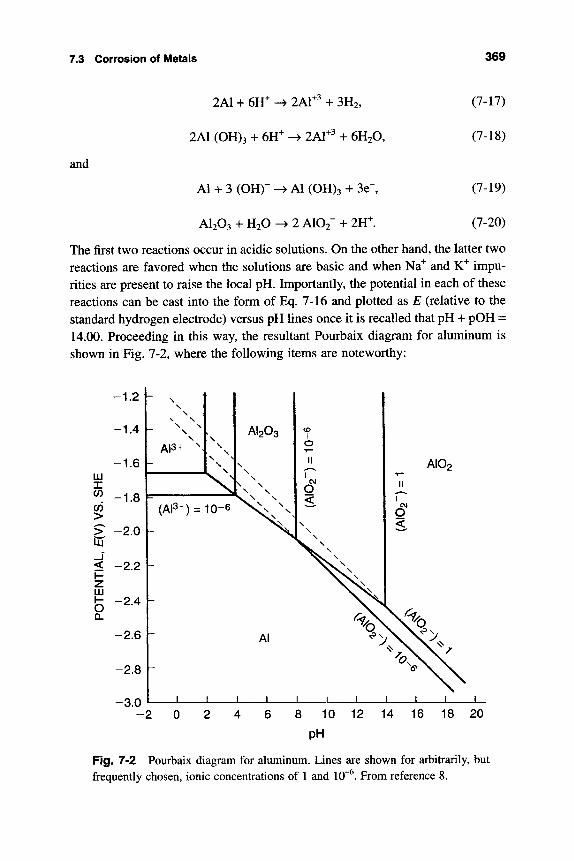
7.3 Corrosion of Metals 369
and
2A1 + 6H^ -> 2Ar^ + 3H2,
2A1 (OH)3 + 6H^ -^ 2Ar^ + 6H2O,
Al + 3 (OH)' -^ Al (OH)3 + Be",
AI2O3 + H2O -^ 2 AIO2" + 2H^.
(7-17)
(7-18)
(7-19)
(7-20)
The first two reactions occur in acidic solutions. On the other hand, the latter two reactions are favored when the solutions are basic and when Na^ and K" impu-rities are present to raise the local pH. Importantly, the potential in each of these reactions can be cast into the form of Eq. 7-16 and plotted as E (relative to the standard hydrogen electrode) versus pH lines once it is recalled that pH + pOH = 14.00. Proceeding in this way, tiie resultant Pourbaix diagram for aluminum is shown in Fig. 7-2, where the following items are noteworthy:
m X CO
CO
> > tu -J < H Z UJ
s Q.
-1 .2
-1 .4
-1 .6
-1 .8
-2 .0
-2 .2
-2 .4
-2 .6
-2 .8
-3 .0
\ \ \
\ AJ3+ -
_
1 \ ! \
L ^ ' ^V \
AI2O3
k \
K \ V \ \
(A|3+) = io-6 X ; ^ N ^ ^Sx
CO
1 0
II
1
0
s \
v
-
r
1" Al
Y
1 J L - 1 J J \
AlOp
>.
J_ J - -1_ _L 8 10 12 14 16 18 20
pH
Fig. 7-2 Pourbaix diagram for aluminum. Lines are shown for arbitrarily, but frequently chosen, ionic concentrations of 1 and 10~ . From reference 8.
370 Environmental Damage to Electronic Products
1. Aluminum is amphoteric, and the protective oxide film dissolves at both low and high pH values. In acids, aluminum dissolves, forming Al "*" ions, while in basic solutions corrosion occurs with the generation of A102~ ions.
2. There is a region of passivity extending between pH 4 to 8, where aluminum is protected by AI2O3. Passivation also requires a potential above —1.8V.
3. Lower concentrations of ions containing Al compress the field of oxide sta-bility.
4. Aluminum metal is immune to corrosion at potentials that lie below those indicated by the lowest lines on the Pourbaix diagram.
7.3.3 Corrosion Rates
In assessing reliability it is the rates of corrosion that are of interest. Corrosion rates are not predictable from thermodynamic considerations and cannot be determined from Pourbaix diagrams. Rather complex processes at the metal-electrolyte interface generally govern the speed of corrosion reactions, and these proceed at finite rates. If the discharge of hydrogen is not rapid enough to accommodate all of the electrons provided, the cathode surface charges nega-tively. The negative potential that develops is known as cathodic polarization. Similarly, anodic polarization, or a positive potential, develops at the anode because of a depletion of electrons. And with greater electron deficiencies, higher anodic polarizations are produced. This, in turn, favors more dissolution of metal or corrosion. Thus we may view anodic polarization as the driving force for corrosion. What happens is that the surface reaches a steady-state potential that depends on the rate at which electrons are exchanged between anode and cathode reactions. Without polarization the smallest driving force would result in infinitely large electrochemical reaction rates.
Irrespective of the specific metals or aqueous environment, Faraday's law determines the extent of damage done. Thus, the passage of 96,500 Coulombs (C) of charge will remove a gram equivalent weight of anode metal and dis-charge a like weight of ions at the cathode. Because corrosion occurs heteroge-neously, corrosion currents are usually unknown. This makes it difficult to pre-dict the extent of corrosion damage and the life of involved components.
7.3.4 Damage Manifestations
Corrosion damage in microelectronics is similar to that which occurs in materi-als used in mechanically functional applications. Although the morphology of corrosive attack can vary appreciably, there are several basic mechanisms, and these are presented in turn.
7.3 Corrosion of Metals 371
7.3.4.1 Uniform Corrosion In this case corrosion damage occurs uniformly over large areas of metal or alloy surfaces. Low-carbon steels and copper alloys are subject to such attack. In the passive state the rate of corrosion is essentially negligible. Protection is typically provided by a thin oxide film. However, if pas-sivity is destroyed by puncturing the oxide, the metal becomes active, with effective anodic and cathodic sites constantly shifting, so that metal loss is uni-form. Although it is relatively easy to protect against uniform corrosion, exam-ples of failures by this mechanism are generally rare.
7.3.4.2 Galvanic Corrosion Two different metals (alloys) are required for galvanic action, perhaps the easiest form of corrosion to recognize. When dis-similar metals in electrical contact are immersed in an electrolyte, an electro-chemical cell (i.e., a battery) is produced. The more active metal becomes the negatively charged electrode, or anode, while the more noble metal becomes the positively charged electrode, or cathode.
Galvanic corrosion is magnified when the anode is small and the cathode large. Examples of such a size effect occur commonly in electronics when elec-trodeposited noble metal coatings are used to protect less noble substrates, e.g., Au on Ni. If the Au coating is porous or punctured at a point, Ni may rapidly corrode. The reason has to do with conservation of current /(A) in both electrode reactions. Thus, if 7 is the current density (A/cm^) and A^ is the electrode area, the condition that /(Au) = /(Ni) means that7(Au)Ao (Au) =7(Ni)Ao(Ni). Because Ao(Au) > AQ (Ni),7(Ni) >7(Au); the high current density causes the small unpro-tected Ni region to rapidly dissolve, while the cathode reaction is collectively borne by the large coating area.
7.3.4.3 Pitting Corrosion As the description implies, pit or hole formation is the form of attack during pitting corrosion. Localized pitting attack generally occurs while the bulk of surface is passive. Chloride, and other halogen ions to a lesser extent, are notorious for initiating pitting attack in otherwise passive metals and alloys. A suggested mechanism for the pitting of stainless steel in the presence of CI" ions is shown in Fig. 7-3. Corrosion begins with the loss of passivity caused by the local destruction of the thin chromium oxide passive film. A copious production of Fe " ions attracts CI", where hydrolysis occurs by the reaction
Fe^^ + 2 H2O -K 2 C r ^ Fe(OH)2 + 2HC1. (7-21)
In the process, Fe(OH)2 forms, and the pH is lowered at the pit initiation site. The acid chloride solution further accelerates anodic dissolution, which in turn concentrates more chloride at the pit, etc., in this so-called self-propagating
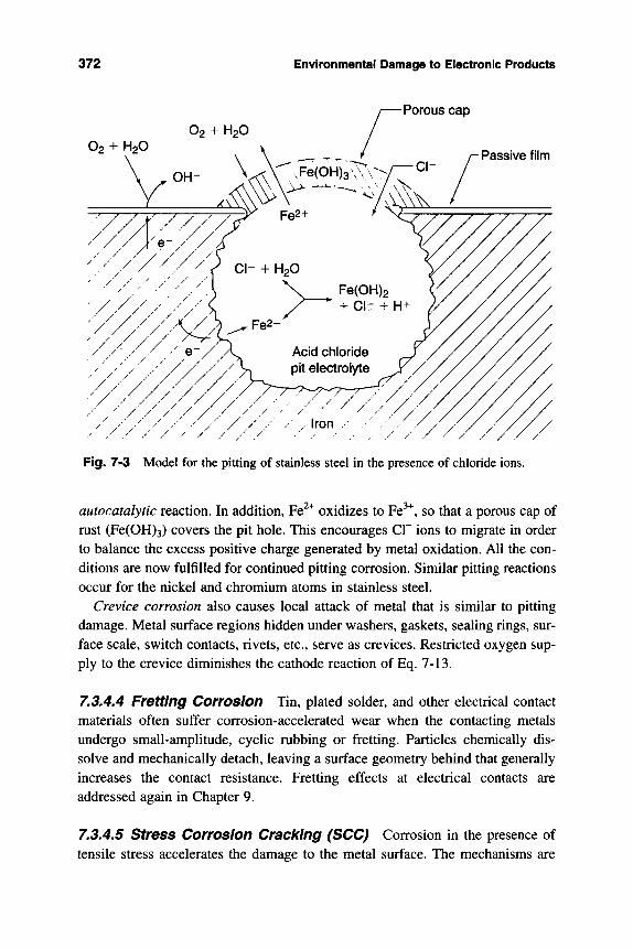
372 Environmental Damage to Electronic Products
Porous cap
O2 + H2O O2 + H2O
Passive film
Fig. 7-3 Model for the pitting of stainless steel in the presence of chloride ions.
autocatalytic reaction. In addition, Fe " oxidizes to Fe "*", so that a porous cap of rust (Fe(0H)3) covers the pit hole. This encourages CI" ions to migrate in order to balance the excess positive charge generated by metal oxidation. All the con-ditions are now fulfilled for continued pitting corrosion. Similar pitting reactions occur for the nickel and chromium atoms in stainless steel.
Crevice corrosion also causes local attack of metal that is similar to pitting damage. Metal surface regions hidden under washers, gaskets, sealing rings, sur-face scale, switch contacts, rivets, etc., serve as crevices. Restricted oxygen sup-ply to the crevice diminishes the cathode reaction of Eq. 7-13.
7.3A.4 Fretting Corrosion Tin, plated solder, and other electrical contact materials often suffer corrosion-accelerated wear when the contacting metals undergo small-amplitude, cyclic rubbing or fretting. Particles chemically dis-solve and mechanically detach, leaving a surface geometry behind that generally increases the contact resistance. Fretting effects at electrical contacts are addressed again in Chapter 9.
7.3.4.5 Stress Corrosion Cradling (SCC) Corrosion in the presence of tensile stress accelerates the damage to the metal surface. The mechanisms are
7.4 Corrosion in Eiectronics 373
not well understood, but it is thought that applied or internal stress causes atoms to leave the anodic tips of incipient cracks, thereby sharpening them. Usually, particular environment-metal combinations are associated with SCC, e.g., chlo-rides for stainless steel, anmionia for copper, and H2S for low-carbon steel. Residual thermal stresses, or those induced by bending electrical lead wires, in combination with moisture serve to promote such cracking. When the loading is cyclic rather than static, the stress-corrosion damage is known as corrosion fatigue.
7.3.4.6 Atmospheric Corrosion This form of corrosion attack stems from the environment, but without the presence of a bulk electrolyte. Instead, the elec-trolyte is usually a thin film of moisture that condenses from the atmosphere when the relative humidity is sufficiently high. The electrolytic process of metal migra-tion on nominally insulating substrates occurs in this manner (Sect. 7.4).
7.4 CORROSION IN ELECTRONICS
7.4.1 Overview
After having just introduced some of the classic manifestations of corrosion, we now focus on corrosion failure in electronic components. A couple of corrosion case histories are reproduced in Fig. 7-4 and discussed in the figure captions. In microelectronic devices the scale of damage is far smaller but no less destructive. Vulnerable metal structures are thin film-contacts, interconnect lines, and wire or solder bonding pads (10, 11). These structures are often coated with glassy inor-ganic and/or organic polymers, which not only provide electrical insulation but mechanically protect and chemically passivate devices as well. However, defec-tive coatings and packages render unprotected metals vulnerable to chemical attack from moisture as well as atmospheric and encapsulant contaminants.
An old but still instructive review by Schnable et fl/.(12) of corrosion in IC chips encased within hermetically sealed and plastic-encapsulated packages has usefully classified corrosion as
1. chemical (where no bias voltage is present), 2. electrochemical (where a dc bias voltage is applied and currents flow), and 3. galvanic (involving dissimilar metals).
The role of the passivating layers is of crucial significance in the corrosion of underlying metals. Pinholes and cracks in these brittle dielectric films (Si02,

374 Environmental Damage to Electronic Products
Fig. 7-4 Examples of corrosion-related problems in electronics, (a) Core of failed nichrome-film resistor showing missing metal. The resistor was damaged by exces-sive heat applied during the lead retinning operation. This opened the resistor epoxy end-cap seal and allowed entry of chlorides from flux and cleaning solvents. Because chlorine was detected in the region of nichrome loss, the role of this element in fostering corrosion attack was confirmed. From J. D. Guttenplan, Materials Perfor-mance, p. 76, April (1990).
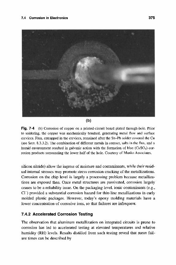
7.4 Corrosion in Electronics 375
Fig. 7-4 (b) Corrosion of copper on a printed-circuit board plated through-hole. Prior to soldering, the copper was mechanically brushed, generating metal flow and surface crevices. Flux, entrapped in the crevices, remained after the Sn-Pb solder covered the Cu (see Sect. 8.3.3.2). The combination of different metals in contact, salts in the flux, and a humid environment resulted in galvanic action with the formation of blue (CUSO4) cor-rosion products surrounding the lower half of the hole. Courtesy of Manko Associates.
silicon nitride) allow the ingress of moisture and contaminants, while their resid-ual internal stresses may promote stress corrosion cracking of the metallizations. Corrosion on the chip level is largely a processing problem because metalliza-tions are exposed then. Once metal structures are passivated, corrosion largely ceases to be a reliability issue. On the packaging level, ionic contaminants (e.g., Cr) provided a substantial corrosion hazard for thin-line metallizations in early molded plastic packages. However, today's epoxy molding materials have a lower concentration of corrosive ions, so that failures are infrequent.
7.4.2 Accelerated Corrosion Testing
The observation that aluminum metallization on integrated circuits is prone to corrosion has led to accelerated testing at elevated temperatures and relative humidity (RH) levels. Results distilled from such testing reveal that mean fail-ure times can be described by
376 Environmental Damage to Electronic Products
MTTF = AV-"" (RH)"" exp f^ , (7-22) m where V is the applied voltage, E^ is an effective activation energy, A, n, and m are constants, and kT has the usual meaning. If the test voltages, circuit designs, and specimen geometry and spacings are constant. Peck (13) has sug-gested that
M T T F » ( R H ) - ^ e x p | ^ ^ [" (7-23)
Like similar formulas that describe electromigration (Eq. 5-31) and dielectric breakdown (Eq. 6-10), Eq. 7-22 is quite useful in design and for making life pro-jections. Unfortunately, however, little insight into the kinetics of the degrada-tion process can be gleaned from such phenomenological formulas.
While early test conditions varied widely, much testing is presently carried out at 85°C and 85% RH. Highly accelerated stress tests (HAST) are popular in order to accentuate the adverse roles humidity and temperature have on corro-sion; otherwise, testing times are impracticably long. Results of a wide survey of available corrosion-failure data for aluminum in epoxy packages are shown in Fig. 7-5. Relative to the standard 85°C/85% RH test conditions, higher temper-atures shorten failure times according to Eq. 7-23.
7.4.3 Corrosion of Specific IVIetals
7.4,3,1 Aluminum Corrosion effects have been widely studied in aluminum and Al base alloy metallizations. As we have already seen, Al suffers corrosion damage in the presence of water. Even the passive, amorphous native-oxide layer can undergo hydrogen blistering damage by the reaction sequence depicted in Fig. 7-6 (14). Most commonly, however, Al corrodes at both anodic and cathodic sites in the presence of contaminant ions. For example, chloride ions from the atmosphere, solder fluxes, chlorinated hydrocarbons (Freon^ trichloroethylene), solvents, etc., accelerate a pitting-type anodic corrosion reac-tion that is autocatalytic via the following cycle:
1. Dissolution of protective hydrated oxide upon adsorption of CI" ions
Al(OH)3 + C r -^ Al(OH)2Cl + OH" (7-24a)
2. Chloride attack of Al
Al + 4Cr -> AICI4" 4- 3e" (7-24b)
3. Regeneration of CI"
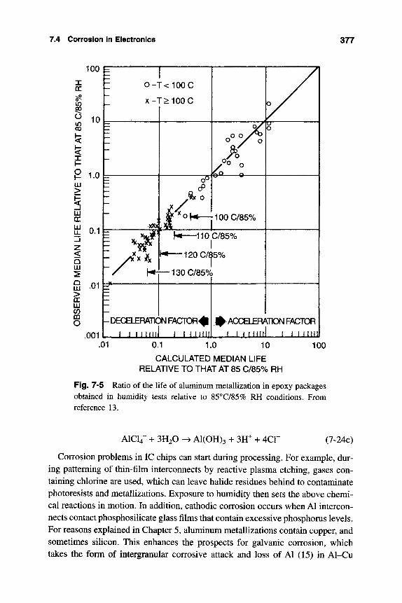
7.4 Corrosion in Electronics 377
100 I DC
in CO O in 00
< I
LU >
I LU CC LU
< Q LU
LU > DC LU CO CQ O
10
1.0
0.1
.01
.001
O - K 1 0 0 C
x - T > 1 0 0 C
#
/ '
Tv^ ""f
i^o ^ o
I h^ 1 IOC/85%
I 120C/85%
•130C/85%
DECELERATION FACTDR^I
I I II mil i I i mil
j ^ ACCELERATION FACTOR
I t iHHil I I i m m .01 0.1 1.0 10
CALCULATED MEDIAN LIFE RELATIVE TO THAT AT 85 C/85% RH
100
Fig. 7-5 Ratio of the life of aluminum metallization in epoxy packages obtained in humidity tests relative to 85°C/85% RH conditions. From reference 13.
AICI4- + 3H2O -^ A1(0H)3 + 3}t + 4Cr (7-24c)
Corrosion problems in IC chips can start during processing. For example, dur-ing patterning of thin-film interconnects by reactive plasma etching, gases con-taining chlorine are used, which can leave halide residues behind to contaminate photoresists and metallizations. Exposure to humidity then sets the above chemi-cal reactions in motion. In addition, cathodic corrosion occurs when Al intercon-nects contact phosphosilicate glass films that contain excessive phosphorus levels. For reasons explained in Chapter 5, aluminum metallizations contain copper, and sometimes silicon. This enhances the prospects for galvanic corrosion, which takes the form of intergranular corrosive attack and loss of Al (15) in Al-Cu
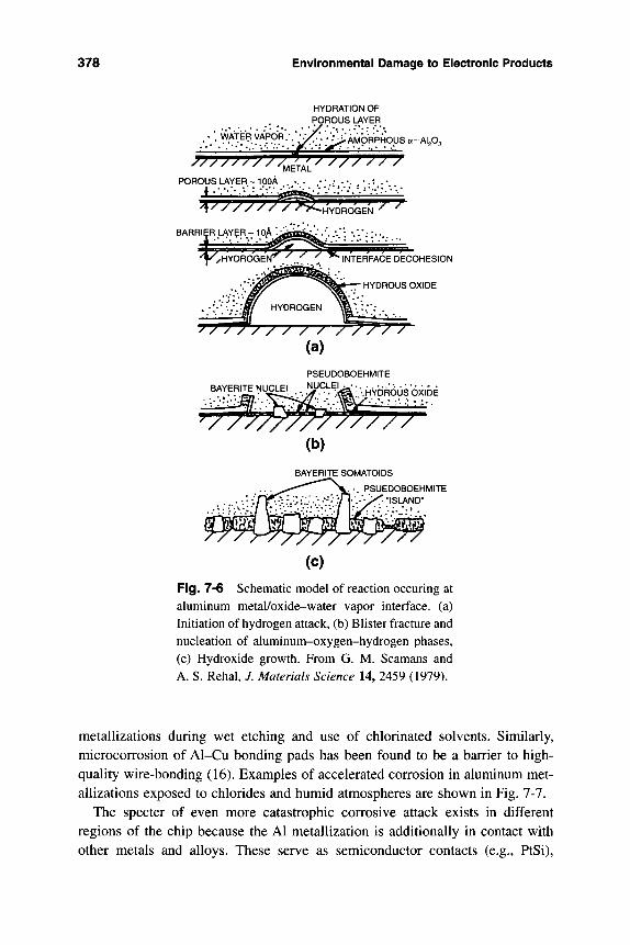
378 Environmental Damage to Electronic Products
HYDRATION OF POROUS LAYER
.; . ; W A T E R y A P d R / ; ^ „ _ A i p ^
POROUS LAYER ~ 10OA . -. . . • ; . : , • / ; . • : • • . • • . .
PSEUDOBOEHMITE
BAYERITE NUCLEI . NU^'-^Ls^* • H V D R O U S OXIDE
. PSUEDOBOEHMITE "ISLAND"
(c) Fig. 7-6 Schematic model of reaction occuring at aluminum metal/oxide-water vapor interface, (a) Initiation of hydrogen attack, (b) Blister fracture and nucleation of aluminum-oxygen-hydrogen phases, (c) Hydroxide growth. From G. M. Scamans and A. S. Rehal, 7. Materials Science 14, 2459 (1979).
metallizations during wet etching and use of chlorinated solvents. Similarly, microcorrosion of Al-Cu bonding pads has been found to be a barrier to high-quality wire-bonding (16). Examples of accelerated corrosion in aluminum met-allizations exposed to chlorides and humid atmospheres are shown in Fig. 7-7.
The specter of even more catastrophic corrosive attack exists in different regions of the chip because the Al metallization is additionally in contact with other metals and alloys. These serve as semiconductor contacts (e.g., PtSi),
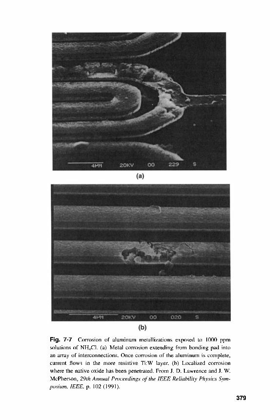
wmmmmgggiMI^^ i
(b)
Fig. 7-7 Corrosion of aluminum metallizations exposed to 1000 ppm solutions of NH4CL (a) Metal corrosion extending from bonding pad into an array of interconnections. Once corrosion of the aluminum is complete, current flows in the more resistive Ti:W layer, (b) Localized corrosion where the native oxide has been penetrated. From J. D. Lawrence and J. W. McPherson, 29th Annual Proceedings of the IEEE Reliability Physics Sym-posium, IEEE, p. 102 (1991).
379
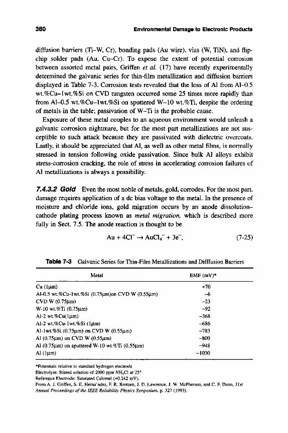
380 Envirohmentar Damage to Electronic Products
diffusion barriers (Ti-W, Cr), bonding pads (Au wire), vias (W, TiN), and flip-chip solder pads (Au, Cu-Cr). To expose the extent of potential corrosion between assorted metal pairs. Griff en et al (17) have recently experimentally determined the galvanic series for thin-film metallization and diffusion barriers displayed in Table 7-3. Corrosion tests revealed that the loss of Al from Al~0.5 wt.%Cu-lwt.%Si on CVD tungsten occurred some 25 times more rapidly than from Al-0.5 wt.%Cu-lwt.%Si on sputtered W-10 wt.%Ti, despite the ordering of metals in the table; passivation of W-Ti is the probable cause.
Exposure of these metal couples to an aqueous environment would unleash a galvanic corrosion nightmare, but for the most part metallizations are not sus-ceptible to such attack because they are passivated with dielectric overcoats. Lastly, it should be appreciated that Al, as well as other metal films, is normally stressed in tension following oxide passivation. Since bulk Al alloys exhibit stress-corrosion cracking, the role of stress in accelerating corrosion failures of Al metallizations is always a possibility.
7.4.3,2 Gold Even the most noble of metals, gold, corrodes. For the most part, damage requires application of a dc bias voltage to the metal. In the presence of moisture and chloride ions, gold migration occurs by an anode dissolution-cathode plating process known as metal migration, which is described more fully in Sect. 7.5. The anode reaction is thought to be
Au + 4Cr -^ AuCU" + 3e", (7-25)
Table 7-3 Galvanic Series for Thin-Film Metallizations and Difffusion Barriers
Metal
Cu (Ijim)
Al-0.5 wt.%Cu-lwt.%Si (0.75^m)on CVD W (0.55^m)
CVD W (0.75^m)
W-10 wt.%Ti (0.75^im)
Al-2 wt.%Cu(l|xm)
Al-2 wt.%Cu-lwt.%Si (l|Xm)
Al-lwt.%Si (0.75^m) on CVD W (0.55^lm)
Al (0.75|im) on CVD W (0.55fxm)
Al (0.75^m) on sputtered W-10 wt.%Ti (0.55^m)
Al ( l^m)
EMF (mV)*
-1-70
-6 -23 -92
-368
- 6 8 6
- 7 8 3
- 8 0 0
-948
-1030
•Potentials relative to standard hydrogen electrode Electrolyte: Stirred solution of 2000 ppm NH4CI at 25°. Reference Electrode: Saturated Calomel (+0.242 mV). From A. J. Griffen, S. E. Hema'ndez, F. R. Brotzen, J. D. Lawrence, J. W. McPherson, and C. F. Dunn, 31st Annual Proceedings of the IEEE Reliability Physics Symposium, p. 327 (1993).

7.4 Corrosion in Electronics 381
while the reverse reaction at the cathode results in dendritic Au deposits that often cause leakage currents or shorting of components. This type of electrolytic corrosion has also been observed in gold-containing metallizations, e.g., Ti-Pd-Au, Ni-Au-Cr, Ti-W-Au, and Ti-Pt-Au.
Polymer-encapsulated gold-wire bonds to aluminum pads have been reported to corrode when there is sufficient moisture permeation of the package (18). Not only is there the AUAI2 (purple plague—see Sect. 5.3.4) compound to contend with, but the epoxy flame-retardants used contain halogens, which provide the Br~ necessary to autocatalyze local pitting corrosion.
Gold is commonly employed in GaAs MESFET contact and metallization schemes. Accelerated temperature-humidity-ionic contamination testing not surprisingly revealed that Al gate electrodes were more susceptible to corrosion damage than Au/refractory metal gates (19). Corrosion of Al, migration of Au between source and gate, shorting metallic bridges, and formation of Al-Au compounds correlated with degradation of device characteristics.
7.4.3.3 Other Metals A number of other metals are used in electronic appli-cations, and a brief survey of corrosion damage in these follows.
a. Nickel Nickel-plated components and hardware are widely used in elec-tronics. An example of nickel corrosion in solid-state microwave hybrid-blocking and bypass capacitors has been reported by Torkington and Lamoreaux (20). Fail-ure in Ni, a normally corrosion-resistant metal, was attributed to the sealed-in moisture derived from the cover gas used during package solder sealing. With condensed moisture, the galvanic voltage (-1.75 V between Au and Ni) added to the larger applied voltage (5 V). In the presence of chlorine and CO2, NiCl2 and NiCOs corrosion products were observed to short the capacitor electrodes. Inter-estingly, the 50:1 Au:Ni ratio is an example of the corrosion-prone, small anode-large cathode configuration (Sect. 7.3.4.2). In this case it greatly increased the current density and attack of nickel.
b. Copper For fear of contaminating and poisoning silicon, copper is spar-ingly used in microelectronics. Nevertheless, there has been recent research and development work on Cu-based, thin-film metallizations (21). Despite its rela-tively minor present role on the chip level, copper and its alloys play a very major role in electrical components such as wire, lead frames, printed-circuit board circuitry, heat sinks, vacuum-tube electrodes and RF gaskets, as well as in systems that cool electronics. Much of the corrosion damage in these items is attributable to attack by atmospheric pollutants, in particular (NH4)2S04 (1). In the presence of sufficient moisture, copper dissolves in ammonium sulfate solu-tion to form Cu(NH3)2' ; i.e..
382 Environmental Damage to Electronic Products
Cu + 2NH3 -^ Cu(NH3)2'' + e". (7-26a)
The corrosion products CU2O and hydrated copper sulfates then form via the fol-lowing typical reactions:
2Cu(NH3)2' + H2O -^ CU2O + 2H+ + 4NH3 (7-26b)
and
SCu "" + 4(0Hr^ +S04^" -^ Cu3(S04)(OH)4. (7-26c)
Copper is also susceptible to corrosion in humid sulfide atmospheres (22). Dendrites of corrosion products were observed to grow laterally from intercon-nections on printed-circuit boards in the absence of applied electric potentials. However, the processes of corrosion, dendrite growth, and filament shorting are accelerated by several orders of magnitude when electric fields are present.
7.4.3.4 Corrosion in H/lagnetic Disl(S Among the metal-containing elec-tronic products sensitive to corrosion are computer hard disks (23, 24). Magnetic recording media typically consist of a layer of either Fe203 particles or a thin metal-alloy (Co-Ni) film sandwiched between an aluminum-substrate pad on the bottom, and metal oxide plus lubricant film on top. Common corrodents were found to be chlorine and sulfur. In the form of S04^~, the latter attacked the Co, which was found on the disk surface.
7.4.4 Modeling Corrosion Damage
Over the years there have been numerous attempts to model corrosion damage with the objective of predicting failure times. This is an extraordinarily difficult task because:
1. the chemical reactions are often complex; 2. ion movements occur in an electrolyte fluid under the influence of spatially
complex electric fields, concentration gradients, and convective flows; and 3. the metal surface structure, chemistry, and heterogeneous nature of damage are
not well known, particularly under conditions of pitting or stress corrosion.
For these reasons it has been common to use familiar, phenomenological for-mulas like Eq. 7-22 to predict failure times. However, these have obvious short-comings, as noted earlier. The approach taken by Pecht (24) and reproduced here is more satisfying, particularly because it connects uniform corrosion rates to reliability functions. To see how, we consider degradation of microelectronic packages that is caused by the two-step process of moisture permeation of pack-ages followed by uniform corrosion of the metallization within.
7.4 Corrosion in Electronics 383
An equation describing permeation of moisture was given earlier (Eq. 7-8):
^ = l - e x p [ - p r ] , (7-27)
where p = Qs/(Po ^ WBIJ^^'^- It is further assumed that uniform corrosion is essentially described by a first-order chemical reaction of the form
^ = - a ( C - C o ) . (7-28) at
In this equation, C may be thought of as a corrosion density per unit volume or concentration, with Q being the maximum, or self-limiting, value of C; i.e., 0 < C < Q . Thus, the rate of corrosion is greatest initially when C = 0 and declines thereafter. Rate constant a combines a product of terms including the relative humidity (RH) in the package and the ubiquitous Boltzmann factor, exp [-EJkT], where E^ is the activation energy for corrosion and kT has the usual meaning. Explicitly, a = ao(RH) exp [-EJkT], where factor a^ is depen-dent on the nature of the materials and voltage bias level.
The effect of temperature is often not what one might expect. When the inter-nal package temperature is higher than the ambient temperature, moisture cannot condense. Thus devices that dissipate a lot of heat may actually suffer less cor-rosion damage than devices that consume and dissipate little power, e.g., CMOS devices. Moisture condenses more readily in the latter, and there is greater cor-rosion risk for metallizations, wirebonds, leadframes, etc.
Since a measure of RH is Pi(t)/PQ, for humidity conditions that allow for con-densed moisture on metallic components, Eq. 7-28 yields
^ ^ = -B(l - exp [- p t]) (C - Co), (7-29) at
where constant B = a^ exp [-EJkT\. Upon separation of variables and integra-tion.
C{t) - Co ^ _ ^ = exp L-i C-o
- | { p ^ - ( l - e x p - p O } (7-30)
The constant of integration Q satisfies the initial condition that at ^ = 0, C = Q. If we now expand the term (P f - (1 - exp [- p f])} a s p ? - l - i - l - p f - l -|(P tf + . . . , or |(p tf for times of order t^, then
Cit) - Co —^ - = exp
C - C
-\BU (7-31)
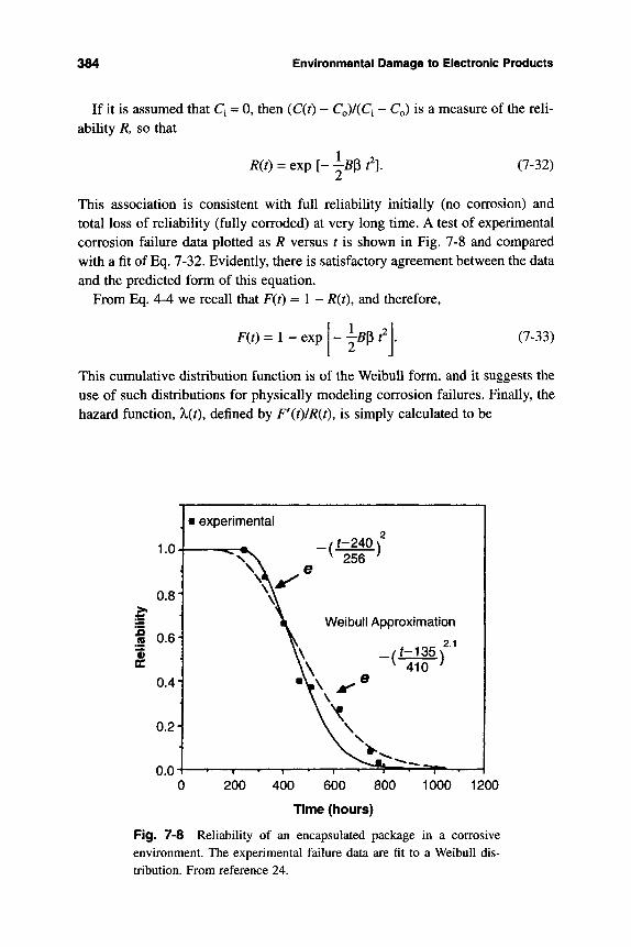
384 Environmental Damage to Electronic Products
If it is assumed that Q = 0, then (C(t) abiUty R, so that
QVCQ ~ Q ) is a measure of the reU-
R(t) = cxp[-^B^t\ (7-32)
This association is consistent with full reliability initially (no corrosion) and total loss of reliability (fully corroded) at very long time. A test of experimental corrosion failure data plotted as R versus t is shown in Fig. 7-8 and compared with a fit of Eq. 7-32. Evidently, there is satisfactory agreement between the data and the predicted form of this equation.
From Eq. 4-4 we recall that F(t) = 1 - R{t), and therefore,
F(0=l-exp[-|5p^ (7-33)
This cumulative distribution function is of the WeibuU form, and it suggests the use of such distributions for physically modeling corrosion failures. Finally, the hazard function, A.(0, defined by F\t)/R(t), is simply calculated to be
I • experimental
Time (hours)
Fig. 7-8 Reliability of an encapsulated package in a corrosive environment. The experimental failure data are fit to a Weibull dis-tribution. From reference 24.
7.5 Metal Migration 385
B^ t exp
'kit) - J - = Bp f.
\mf (7-34) exp
This result corresponds directly to the Rayleigh failure rate (see Sect. 4.3.3).
7.5 METAL MIGRATION
7.5.1 Introduction
The phenomenon of metal migration, also referred to as "metallic," "wet," and "electrolytic" electromigration, has caused many catastrophic microcircuit failures (22, 25). Unlike solid-state electromigration (Sect. 5.5), which generally requires elevated temperatures and high current densities ('- 10^ A/cm^), metal migration can occur at room temperature with passage of less than 1 x 10"^ A/cm^. Like cor-rosion, it is an electrochemical phenomenon that can occur both within and outside of IC packages. The effect was first observed in polymer (phenol fiber) circuit boards containing silver lead wires and contacts. In essence, Ag metal was ionically removed from its initial location, then Ag ions migrated in the electric field, and finally Ag metal redeposited elsewhere (26). Water adsorbed on the insulator sur-face served as the electrolyte. At the anode, Ag formed a colloidal oxide, while at the cathode Ag metal assumed the dendritic morphology. Examples of dendritic growth in silver and copper conductors are shown in Figs. 7-9a and b.
An extensive review of metal migration-accelerated testing (27) suggests that the effects are largest in silver. In addition to Ag, metals that migrate in a dis-tilled water electrolyte include Bi, Cd, Cu, Pb, Sn, and Zn. When distilled water is contaminated with sodium or potassium chloride (0.001 to 0.01 M), Au, Pd, and Pt migrate. Other metals, e.g., Ni, Cr, and Ag-Au-Pd alloys, also migrate under certain conditions. When liquid water is present, electromigration effects increase greatly in speed and severity.
For metal migration to occur, the following conditions are generally required:
1. The anode metal must easily form ions. 2. Nearby there must be a metal that serves as the cathode. 3. A dc voltage must exist between the anode and cathode. Depending on the inter-
electrode spacing, as little as 1 to 2 V up to 100 V or more may be required. 4. Moisture or a water film must be present on the insulator substrate surface to
provide the electrolyte needed for ionic conduction. Porous and fibrous sub-strates, e.g., epoxy resin/glass fiber, polyesters, laminates, and fabrics, serve to retain the electrolyte.
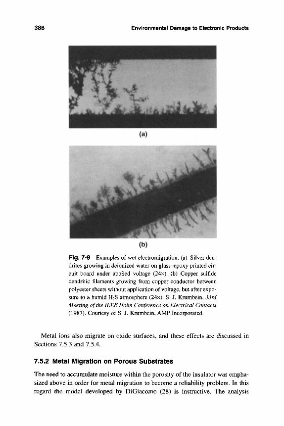
386 Environmental Damage to Electronic Products
Fig. 7-9 Examples of wet electromigration. (a) Silver den-drites growing in deionized water on glass-epoxy printed cir-cuit board under applied voltage (24x). (b) Copper sulfide dendritic filaments growing from copper conductor between polyester sheets without application of voltage, but after expo-sure to a humid H2S atmosphere (24x). S. J. Krumbein, 33rd Meeting of the IEEE Holm Conference on Electrical Contacts (1987). Courtesy of S. J. Krumbein, AMP Incorporated.
Metal ions also migrate on oxide surfaces, and these effects are discussed in Sections 7.5.3 and 7.5.4.
7.5.2 Metal Migration on Porous Substrates
The need to accumulate moisture within the porosity of the insulator was empha-sized above in order for metal migration to become a reliability problem. In this regard the model developed by DiGiacomo (28) is instructive. The analysis
7.5 Metal Migration 387
assumes that the metal ion current density that flows is directly proportional to the fraction of substrate pores containing condensed water. For a lognormal distribution of pore radii, the fractional area ( /) on which condensation occurs is given by
/ = - E r f c 2
1 , (r,. - a i m (7-35)
where a (see Sect. 4.3.5) is In (rso/ri^), and r vg is the average pore radius. Water condensation in pores from a saturated vapor pressure (p) is basically driven by a chemical reaction whose free energy change per unit volume AGy is given by -kT In ^ (29). The ratio of the vapor pressure above the pore radius, or menis-cus, n relative to that over a flat pore surface p^, may be thought of as the rela-tive humidity (i.e., RH). In this context, elementary nucleation or capillarity the-ory establishes the connection between r and AGy as r = kTi^RH)^ where y and Q are the water surface tension and atomic volume, respectively, and kT has the usual meaning.
The ionic mass flux (/j) is the product of the ion concentration (Q in g/cm^) and its velocity, where the latter is given by the Nemst-Einstein equation (Eq. 1-6); i.e., Vi = DF/RT. As in electromigration (Sect. 5.5.2), the force F is equal to ZqS', where Z is the ion valence, q is the electronic charge, and S is the electric field. Combining all of the above terms, the equation
^. = ( ^ ^ ^ ) / = Z ^ Q D ^ E r f c RT
a ^ /ravg/:rin(RH) (7-36)
results. The goal is to obtain the time to failure (MTTF), which is defined by how long it takes a dendritic filament to span conductors separated by a length L when a voltage V is applied. To produce and extend a dendrite, the current density at its tip must be orders of magnitude higher than its average value. Dendritic growth occurs by a focusing of the ion current at its tip of radius r , an effect that magni-fies the local field to S^= V/r^. The critical mass of metal that is transported to cre-ate the shorting dendrite filament is assumed to be Lr^ 5 d, where 5 is the elec-trolyte thickness and d is the metal density. Failure occurs in time t = MTTF, and by definition the corresponding mass flux (mass/area-time) is /i = Lr^ 5 d/r^ 5 MTTF = L (i/MTTF. Solving for MTTF yields the desired result
MTTF: r^RTLd
ZqQDVEvfc In ravgi^rinRHN2
2ya
(7-37)
In this closed-form equation, the effects of voltage, humidity, nature of the substrate, dendrite geometry, and temperature (through D and RH) are all linked.
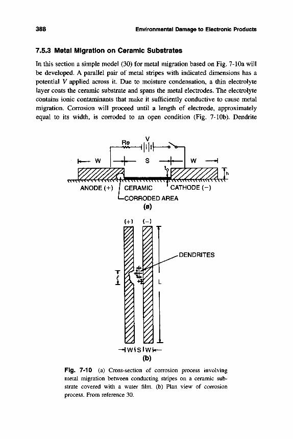
388 Environmental Damage to Electronic Products
7.5.3 Metal Migration on Ceramic Substrates
In this section a simple model (30) for metal migration based on Fig. 7-lOa will be developed. A parallel pair of metal stripes with indicated dimensions has a potential V applied across it. Due to moisture condensation, a thin electrolyte layer coats the ceramic substrate and spans the metal electrodes. The electrolyte contains ionic contaminants that make it sufficiently conductive to cause metal migration. Corrosion will proceed until a length of electrode, approximately equal to its width, is corroded to an open condition (Fig. 7-lOb). Dendrite
W
I ANODE (+) / CERAMIC ' CATHODE (-) -CORRODED AREA
(a)
(+) (-)
DENDRITES
Fig. 7-10 (a) Cross-section of corrosion process involving metal migration between conducting stripes on a ceramic sub-strate covered with a water film, (b) Plan view of corrosion process. From reference 30.
7.5 Metal Migration 389
growth, which can short conductors, is often a secondary effect of corrosion. Using Ohm's law (/ = V/R) and the definition of resistance R{Q) = p 5/(L o), we obtain
• ^^ (7-38) (Sp/O'
where p (Q-cm) is the resistivity of the electrolyte. The volume of corroded metal, v (cm^), is proportional to the total charge Q (C) passed, or / XT, where T is the time. Faraday's law essentially states that Q = n dv FJM, where F^ is the Faraday constant and n, d, and M are the metal valence, density, and atomic weight, respectively. Therefore, combining terms, the effective time to failure (x = MTTF) when v = Iwh, is given by
MXTF = " ^ ^^^^ {^ = constant x p/t^, (7-39) MVL \toJ
where the constant depends on the metal in question and the amount lost, the corrosion geometry, and the applied voltage.
This model predicts that corrosion failure times are directly proportional to the resistivity of the electrolyte divided by its thickness. The quantity p/to is known as the sheet resistance and has the peculiar units of ohms per square. This definition stems from the fact that the electrical resistance of a thin square of material is independent of the size of the square. In thin films or layers, the sheet resistance is measured by probing the wide surface area with a four-point resis-tivity probe. In aqueous solutions the equivalent conductances (A) are given by A = 1000/(pC), and are tabulated for concentrations ( Q of different ionic species (31). This makes it possible to estimate the sheet resistance.
Example 7-1 After introduction of 1.7 ppm of CI2 into an 85°C/80% RH ambient, the corrosion leakage current across metal stripes on a ceramic sub-strate increased. If the moisture layer is 100 nm thick, what is the electrolyte sheet resistance?
Answer Chlorine dissolves in water through the reaction
CI2 (g) + H2O -^ H" + C r -H HOCl,
which is the difference of the half reactions
H2O -H c r -> H^ -f HOCl + 2e-, £^ = +1.49 V,
and
2Cr -> CI2 (g) + 2e-, £^ = +1.36 V.
390 Environmental Damage to Electronic Products
Applying Eq. 7-14,
0 = (1.49 - 1.36) + 8.314 (358) / 2 (96,500) In (H"") (CI") / (Cy.
Substituting for the chlorine concentration, (CI2) = 1.7 x 10"^ yields (H"") (CI") = 3.36 X 10"^ . Thus there are 1.83 x 10 ^ equivalents per liter for each ion. The equivalent conductance of H"" and CI" is 775 at 85°C (31). Since p = 1000/(CA), the sheet resistance, plt^ = 1000/(CA t^). Substitution yields p/t^ = 1000/1.83 x 10"^ (775)(10"^) = 7.1 X 10^ Q/sq.
7.5.4 Mobile Ion Contamination in CMOS Circuits
Related to the problem of ion migration in liquid electrolytes is ion transport through a solid ionic medium like Si02. Though not a corrosion problem, the fact that ionic motion is involved makes it of interest here. One of the most seri-ous reliability problems exhibited by early MOS transistors was instability of the threshold voltage (Vj) causing operation at more negative voltages than desired. With positive bias, VT drifted with time to more negative values. At elevated temperatures device behavior was very erratic. The cause of these problems was drift of positively charged mobile ions in the gate oxide. A particular culprit was identified to be sodium, hence the appellation "the sodium problem." Sodium entered processing lines from the quartzware used as well as from the salt intro-duced by winter footwear. Despite the progress made in tracking down sources of impurities and reducing instabilities due to positive mobile ion contamination, failures due to this cause still occur (32).
Ion drift velocities (v) can be calculated from the measured mobilities (|Li in units of cm^/V-s) through the formula
v = |Li^, (7-40)
where e is the electric field. For Na" and K" in Si02 the respective values of mobility are
i (Na"") = 1.0 exp |^- -5:^-2Y.\ c m W - s (7-41a)
and
|Li (K- ) = 0.03 exp (- ^ ^ Y ^ ) cmW-s . (7-41b)
This means that Na"* ions will traverse a 15 nm thick oxide in 10"^ s at 200°C in fields of 1 MV/cm. On the other hand, the larger K"* ions require about 10 s. Maximun tolerable Na"* and K" concentrations are 1 x 10^^ cm"^. When positive
7.6 Radiation Damage to Electronic l\/laterials and Devices 391
ions drift through the oxide of an MOS structure they also shift the effective flat-band voltage. Thus a positive gate bias voltage applied to NMOS transistors drives ions toward the Si interface and displaces the flat-band voltage by -QIC^ (Sect. 2.5.3), where Q is the ion charge and Q is the oxide capacitance. Equivalently, transistor threshold-voltage shifts occur as a result of charge transport (Eq. 2-6). Such instabilities are not as evident in PMOS transistors, which is the reason these devices were the first to be commercially developed.
7.6 RADIATION DAMAGE TO ELECTRONIC MATERIALS AND DEVICES
7.6.1 A Historical Footnote
It was a "big bang" on July 9, 1962, that catapulted the reliability of radiation-damaged solid-state electronics to the center stage of world politics (33). On that day the U.S. high-altitude nuclear device Starfish was detonated. This was fol-lowed by several similar Russian tests later that year. The resulting nuclear con-tamination of the exoatmosphere generated sufficient electronic perturbation to the Van Allen belt to cause failure of the Telstar 1 communications satellite. Not long after this, Nikita Khrushchev, premier of the USSR, announced that this radiation vulnerability would be considered a possible strategy to destroy future U.S. military space systems. This threat provided an incentive and challenge to develop survivable space electronics and acquire an understanding of the nature of radiation damage to semiconductor devices. Fortunately, the damage to Tel-star was reversible. In time, enough was learned so that damaged p-n junctions could be repaired from the ground by altering their bias voltages.
Even though the cold war is now history, interest persists in the subject of radiation damage to semiconductor devices and electronic equipment used in the peaceful exploitation of nuclear energy. A number of recent books on this and related topics (34, 35, 36) amply demonstrate this interest and importance.
7.6.2 Some Definitions
The radiation we are primarily concerned with is composed of energetic particles and photons possessing energies ranging from tens to millions of electron volts. While the former include neutrons, electrons, and alpha particles. X-rays, gamma rays, and ultraviolet light are examples of photons. The radiation energy density that materials are exposed to is known as the dose (D). If dE is the mean energy absorbed per unit mass dm of irradiated material, the dose is defined by
392 Environmental Damage to Electronic Products
dF D = f^. {IAD
dm
Although the absorbed dose in a small region, i.e., a gate oxide, can be rigor-ously defined, it is impossible to know the actual energy imparted. The common unit of dose is the rad, defined as 1 rad =100 ergs/g. In the SI system the gray (Gy) is the unit of dose, where 1 Gy = 1 J/kg, so that 1 Gy = 100 rads. Since the absorbed dose depends on the material in question, the latter should be refer-enced directly following the dose unit, e.g., rads (Si), rads (Si02), Gy (GaAs).
In many applications the dose rate dD/dt, expressed in rad/s, is important. For example, during exposure to long-lived radioactive isotopes, D is assumed to be constant, and the dose rate is zero. If radiation is pulsed, e.g., flash X-ray machines or a nuclear blast, then the dose rate also becomes a significant vari-able. Examples will be given of cases where D and dD/dt are reported.
7.6.3 Radiation Environments
The primary radiation environments that degrade or damage electronic materials and devices include outer space, nuclear reactors, radiation processing activities, nuclear weapon and controlled fusion facilities (35). Electronic equipment is exposed to these radiation environments during interplanetary space flight, in power generating plants, in factories, and in defense applications.
In outer space particle and photon radiation have typical energies ranging from keV to GeV and consist of
a. a broad spectrum of energetic particles trapped in the earth's magnetic field, forming radiation belts;
b. galactic cosmic rays, which are the fluxes emanating from energetic heavy ions. Energies can extend even beyond TeV;
c. solar winds and flares, which are eruptions of energetic protons and smaller amounts of alpha particles, heavy ions, and electrons with energies ranging to hundreds of MeV.
The nuclear-reactor environment depends on reactor type. Within the core of pressurized-water, boiling-water, and fast-breeder reactors, neutron fluxes range from 10^^ to 10 " cm ^ s \ while gamma-radiation levels between 10 to 10^^ rad/h are common. This contrasts with neutron fluxes of 3 x 10^ cm~^ s~ and gamma ray doses of 10"^ to 10^ rad/h in the containment area where electronic equipment and components operate.
Radiation processing is employed in a number of industrial activities, which are noted together with the doses involved; retardation of food spoilage (30-500 krad), sterilization of medical supplies (2.5 Mrad), sewage processing (-'1

7.6 Radiation Damage to Eiectronic i^lateriais and Devices 393
Mrad), and modification of polymers (10-15 Mrad). The processing of spent nuclear fuels generates maximum dose rates of 10^ rad (Si)/h for ganmia radia-tion and 0.1 rad (Si)/h for neutrons.
In contrast, a 1 megaton nuclear weapon produces prompt radiation dosages of 2100 rad neutrons and 62,000 rad gamma at a distance of 1 mile from the det-onation point. If and when controlled nuclear fusion reactors are a reality, radia-tion levels of 10^^-10^^ equivalent neutrons-cm"^ and ionizing doses of 10^-10^ rad (Si) s~ will have to be dealt with. The primary source of this radiation is 14 MeV neutrons from the deuterium-tritium reaction.
In each of the above environments electronic equipment is used to sense and monitor radiation as well as to control robots and other machinery remotely. To appreciate the damage to solid-state and electro-optical devices that the above radiation magnitudes can wreak, we must first understand how energetic parti-cles and ionizing radiation interact with materials.
7.6.4 Interaction of Radiation with IVIatter
We are primarily concerned with the consequences of atomic displacements and ionization in materials caused by radiation. This broad subject, which has been researched for a half century, does not easily lend itself to a brief review. Nev-ertheless, in flow-chart style. Fig. 7-11 neatly summarizes radiation damage into particle- and photon-induced categories. Of particular interest is the long-lived, as well as transient, damage produced by the particular radiation.
a. Atomic Displacement Starting with particles, we note that physical dis-placement of atoms from their original positions is the major form of damage created. The particle trajectory, and the damage produced, depends on its energy, mass, and charge, as well as on the nature of the matrix. What happens during ion implantation doping of silicon illustrates these effects. Dopant ions with kinetic energies of '-SO-lOO keV, or thousands of times larger than the binding energies of lattice atoms, knock atoms off lattice sites in collision cascades, cre-ating vacancy and interstitial defects in the process. It is usually difficult to esti-mate just how many vacancy-interstitial pairs are created. For example, if the displacement energy is 10 eV, a 12 MeV proton is predicted to generate only 17 vacancy-interstitial pairs (35). Each incoming ion executes a different trajectory and comes to rest at a different depth from the surface. The ion range is statisti-cally distributed, and lighter particles penetrate further than heavier ones of the same energy. Heating the radiation-damaged matrix heals it because atoms again resume their equilibrium positions by diffusional processes.
Materials exposed to an energetic-particle environment may also become radioactive. Protons, neutrons, and nuclei are all capable of transforming stable
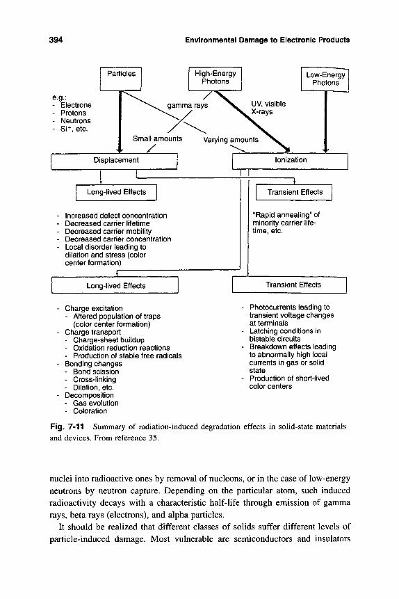
394 Environmental Damage to Electronic Products
Particles High-Energy Photons
e.g.: - Electrons - Protons - Neutrons - Si+,etc.
Increased defect concentration Decreased carrier lifetime Decreased carrier mobility Decreased carrier concentration Local disorder leading to dilation and stress (color center formation)
X Long-lived Effects
Charge excitation - Altered population of traps
(color center formation) Charge transport - Charge-sheet buildup - Oxidation reduction reactions - Production of stable free radicals Bonding changes - Bond scission - Cross-linking - Dilation, etc. Decomposition - Gas evolution - Coloration
"Rapid annealing" of minority carrier life-time, etc.
Transient Effects
- Photocurrents leading to transient voltage changes at terminals
- Latching conditions in bistable circuits
- Breakdown effects leading to abnormally high local currents in gas or solid state
- Production of short-lived color centers
Fig. 7-11 Summary of radiation-induced degradation effects in solid-state materials and devices. From reference 35.
nuclei into radioactive ones by removal of nucleons, or in the case of low-energy neutrons by neutron capture. Depending on the particular atom, such induced radioactivity decays with a characteristic half-life through emission of gamma rays, beta rays (electrons), and alpha particles.
It should be realized that different classes of solids suffer different levels of particle-induced damage. Most vulnerable are semiconductors and insulators
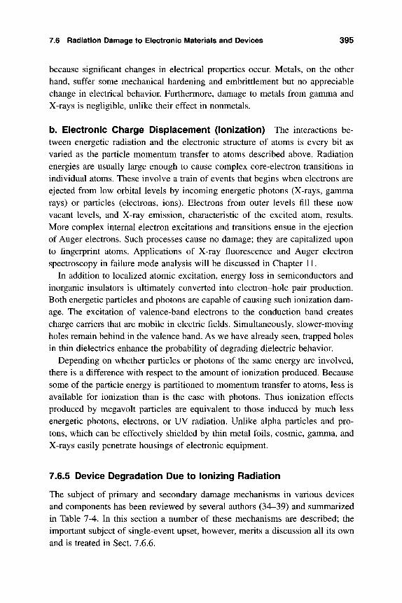
7.6 Radiation Damage to Electronic l\/laterials and Devices 395
because significant changes in electrical properties occur. Metals, on the other hand, suffer some mechanical hardening and embrittlement but no appreciable change in electrical behavior. Furthermore, damage to metals from gamma and X-rays is negligible, unlike their effect in nonmetals.
b. Electronic Charge Displacement (Ionization) The interactions be-tween energetic radiation and the electronic structure of atoms is every bit as varied as the particle momentum transfer to atoms described above. Radiation energies are usually large enough to cause complex core-electron transitions in individual atoms. These involve a train of events that begins when electrons are ejected from low orbital levels by incoming energetic photons (X-rays, gamma rays) or particles (electrons, ions). Electrons from outer levels fill these now vacant levels, and X-ray emission, characteristic of the excited atom, results. More complex internal electron excitations and transitions ensue in the ejection of Auger electrons. Such processes cause no damage; they are capitalized upon to fingerprint atoms. Applications of X-ray fluorescence and Auger electron spectroscopy in failure mode analysis will be discussed in Chapter 11.
In addition to localized atomic excitation, energy loss in semiconductors and inorganic insulators is ultimately converted into electron-hole pair production. Both energetic particles and photons are capable of causing such ionization dam-age. The excitation of valence-band electrons to the conduction band creates charge carriers that are mobile in electric fields. Simultaneously, slower-moving holes remain behind in the valence band. As we have already seen, trapped holes in thin dielectrics enhance the probability of degrading dielectric behavior.
Depending on whether particles or photons of the same energy are involved, there is a difference with respect to the amount of ionization produced. Because some of the particle energy is partitioned to momentum transfer to atoms, less is available for ionization than is the case with photons. Thus ionization effects produced by megavolt particles are equivalent to those induced by much less energetic photons, electrons, or UV radiation. Unlike alpha particles and pro-tons, which can be effectively shielded by thin metal foils, cosmic, gamma, and X-rays easily penetrate housings of electronic equipment.
7.6.5 Device Degradation Due to Ionizing Radiation
The subject of primary and secondary damage mechanisms in various devices and components has been reviewed by several authors (34-39) and summarized in Table 7-4. In this section a number of these mechanisms are described; the important subject of single-event upset, however, merits a discussion all its own and is treated in Sect. 7.6.6.
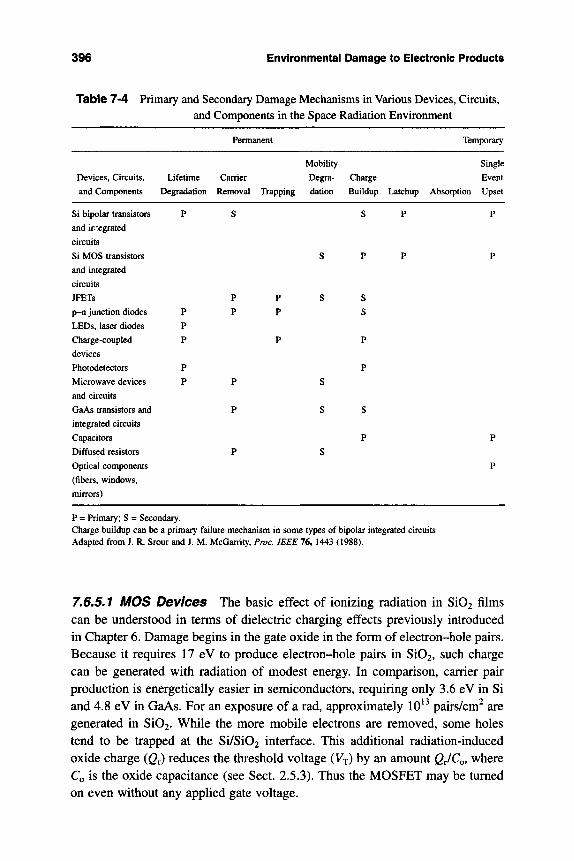
396 Environmental Damage to Electronic Products
Table 7-4 Primary and Secondary Damage Mechanisms in Various Devices, Circuits, and Components in the Space Radiation Environment
Pennanent Temporary
Devices, Circuits,
and Components
Lifetime Carrier
Degradation Removal Trapping
Mobility Single
Degra- Charge Event
dation Buildup Latchup Absorption Upset
Si bipolar transistors
and ir'egrated
circuits
Si MOS transistors
and integrated
circuits
JFETs
p-n junction diodes
LEDs, laser diodes
Charge-coupled
devices
Photodetectors
Microwave devices
and circuits
GaAs transistors and
integrated circuits
Capacitors
Diffused resistors
Optical components
(fibers, windows.
mirrors)
P
P
P
P
P
P
S
P
P
P
P
P
P
P
P
s
s
s
s
s
s
p
s s
p
p
s
p
P = Primary; S = Secondary. Charge buildup can be a primary failure mechanism in some types of bipolar integrated circuits Adapted from J. R. Srour and J. M. McGarrity, Proc. IEEE 76, 1443 (1988).
7.6.5.1 MOS Devices The basic effect of ionizing radiation in Si02 films can be understood in terms of dielectric charging effects previously introduced in Chapter 6. Damage begins in the gate oxide in the form of electron-hole pairs. Because it requires 17 eV to produce electron-hole pairs in Si02, such charge can be generated with radiation of modest energy. In comparison, carrier pair production is energetically easier in semiconductors, requiring only 3.6 eV in Si and 4.8 eV in GaAs. For an exposure of a rad, approximately 10 ^ pairs/cm^ are generated in Si02. While the more mobile electrons are removed, some holes tend to be trapped at the Si/Si02 interface. This additional radiation-induced oxide charge (gr) reduces the threshold voltage (VT) by an amount Qr/Co, where Co is the oxide capacitance (see Sect. 2.5.3). Thus the MOSFET may be turned on even without any applied gate voltage.
7.6 Radiation Damage to Electronic iVIaterials and Devices 397
Threshold-voltage shifts are both dose and dose rate dependent. This is illus-trated in Fig. 7-12 for n-channel MOS devices. At first, VT is unchanged up to doses of approximately 10^ rad (Si02), then it goes negative, where it reaches a minimum and finally swings up toward more positive values as the dose rises. This behavior, which is accentuated by increasing dose rates, is a superposition of two effects. Gate oxide-trapped holes cause a monotonic decrease in VV with dose, while negative interface states induce a rise in V^. Other deleterious effects of radiation in MOSFETs include channel-mobility degradation and increased leakage currents at high dose levels.
7.6.5.2 GaAs Devices In some environments GaAs devices are far more radiation tolerant than Si devices, but in other radiation environments the dam-age is comparable. For example, GaAs FETs have no gate insulators to experi-ence charge buildup and, therefore, are relatively inmiune to radiation. In bulk GaAs, like Si, ionizing radiation generates electron-hole pairs, introduces defect levels and scattering centers in the energy gap, removes carriers, and reduces mobility. The latter two effects are responsible for transconductance or gain degradation in transistors. For this to occur in GaAs, dose levels of --10^ rad are typically required when channel doping levels are relatively high.
0.30
0.20
0.10
g 0.00
8) -0.10
-0.20
-0.30
-0.40
-0.50
-0.60
-0.70
-0.80
T T
0.01 rads (SiOg)/! 0.10
18250.
L ——— Model computations
103 104 I I I ! t i n l I I I I m i l I I I i i i n l
105 106
Ionizing dose rads (Si02)
Fig. 7-12 Threshold voltage for n-channel CMOS transistors as a function of dose for various dose rates. From D. B. Brown, W. C. Jenkins, and A. H. Johnston, IEEE Trans. Nuclear Science 36, 1954 (1989).
398 Environmental Damage to Electronic Products
7.6.5.3 Electro-optical Devices Laser diodes, light emitting diodes, and photodetectors all suffer degradation of operating characteristics due to radiation damage (37). In lasers, permanent increases in threshold currents result from ionizing radiation, which generates nonradiative recombination centers. Thejat-ter are also primarily responsible for degradation of LEDs. Silicon-based pho-todetectors and CCDs are prone to the same degradation mechanisms, i.e., charge buildup, surface leakage currents, reduction in carrier mobility and life-time, that plague MOS devices.
Optical fiber, often used with these devices, offers advantages relative to con-ventional transmission lines because it is insensitive to electromagnetic noise. However, optical fiber is more sensitive to radiation damage in the form of lumi-nescence and increased absorption. Spurious light signals and attenuation of light pulses can then be expected.
In general, the damage and degradation discussed to this point occurs only at high radiation levels that are created artificially. We now consider the often more serious radiation damage that can occur in circuits powered in what would be considered natural, everyday environments.
7.6.6 Soft Errors
7.6.6.1 Introduction Computer circuits function by identifying small packets of charge as elemental bits of information. Any noise that modifies this charge also may change the information stored. This can happen, for example, when radi-ation, a source of this noise, impinges upon and alters the electrical state of an internal node, causing a false logic transition, e.g., a bit flop. Such errors may mean data corruption, execution of wrong commands, or even a "locking up" that requires reinitialization. In digital electronics, errors that are not caused by per-manent damage to circuits are referred to as soft errors, soft fails, or single event upsets (SEU). Soft fails, happily, do not necessarily affect the computer user, because the system may be turned off or the incorrect memory bits may be over-written before they are used. In microelectronic circuits employed in satelHtes, digital avionics, high-flying aircraft, as well as in terrestrial electronics and com-puters, soft errors are a major concern. Over the years from 1970 to 1982 there have been over 40 recorded upsets in space satellites (e.g.. Voyager, Pioneer Venus, Galileo) that affected NMOS, CMOS, and bipolar memories, as well as assorted flip-flop circuits (40). Occasionally, however, the more serious effect of single event latchup (SEL) has been triggered, resulting in circuit destruction.
Soft errors and their reliability implications are sufficiently important to be the subject of an entire recent issue of the IBM Journal of Research and Develop-ment (41). In it there is an interesting history of the IBM experience from 1978
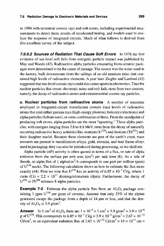
7.6 Radiation Damage to Electronic IVIaterials and Devices 399
to 1994 with terrestrial cosmic rays and soft errors, including experimental mea-surements to detect them, results of accelerated testing, and models used to ana-lyze the response of integrated circuits. Much of what follows is derived from this excellent survey of the subject.
7,6.6.2 Sources of Radiation That Cause Soft Errors In 1978 the first evidence of sea-level soft fails from energetic particle impact was published by May and Woods (42). Radioactive alpha particles emanating from ceramic pack-ages were determined to be the cause of damage. The source was the water used in the factory, built downstream from the tailings of an old uranium mine that con-tained high levels of radioactive elements. A year later Ziegler and Lanford (43) suggested that sea-level cosmic rays could also cause upsets in electronics. Thus the nuclear particles that create electronic noise and soft fails stem from two sources, namely, the decay of radioactive atoms and extraterrestrial cosmic ray particles.
a. Nuclear particles from radioactive atoms A number of materials employed in integrated-circuit manufacture contain trace levels of radioactive atoms that emit either gamma rays (high-energy photons), beta rays (electrons) and alpha particles (helium ions), or some combination of these. From the standpoint of producing soft errors, alpha particles are the most "upsetting." These alpha parti-cles, with energies ranging from 3.8 to 8.8 MeV, stem from the decay of naturally occurring radioactive heavy actinides like uranium (U"^°) and thorium (Th'^0 and their daughter nuclei. Because these elements are part of the earth's crust, trace amounts are present in metallization alloys, gold, alumina, and lead frame alloys used in packaging; they can also be introduced during processing, as we shall see.
Alpha particle (aP) activity is often quoted in terms of a flux, or rate of alpha emission from the surface per unit area (cm^) per unit time (h). As a rule of thumb, an alpha flux of 1 alpha/cm^-h corresponds to one part per million (ppm) of U^ ^ nuclei. The following calculation shows us how to estimate the flux more exactly (44). First we note that U^ ^ has an activity of 6.85 x 10"^ Ci/g, where 1 curie (Ci) = 2.2 x 10^^ disintegrations/min (dpm). Furthermore, the decay of U^ ^ to Pb^^^ releases 8 alpha particles.
Example 7-2 Estimate the alpha particle flux from an AI2O3 package con-taining 1 ppm U^ ^ per gram of ceramic. Assume that only 25% of the alphas generated escape the package from a depth of 14 |im or less, and that the den-sity of AI2O3 is 3.9 g/cml
Answer In 1 cm^ of AI2O3 there are 1 x 10"^ x 1 cm^ x 3.9 g/cm^ = 3.9 x 10"^ g of U^^^ This corresponds to 6.85 x 10"^ Ci/g x 3.9 x 10"^ g/cm^ = 2.67 x 10"^^ Ci/cm^, or an equivalent radiation flux of 2.67 x 10"^^ Ci/cm^ x 14 x 10"^ cm =
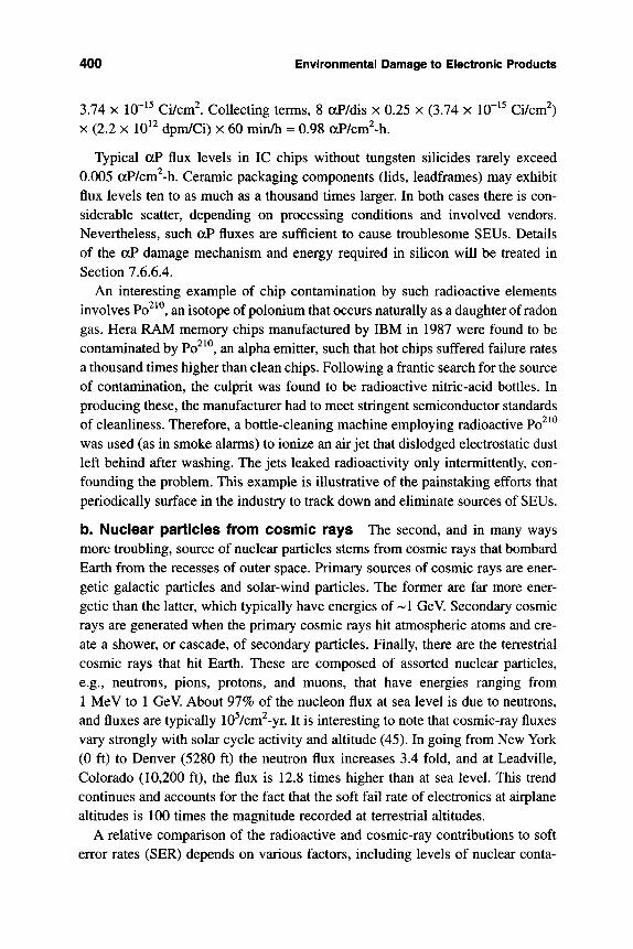
400 Environmental Damage to Electronic Products
3.74 X 10" ^ Ci/cml Collecting terms, 8 aP/dis x 0.25 x (3.74 x 10" ^ Ci/cm^) X (2.2 X 10^^ dpm/Ci) x 60 min/h = 0.98 aP/cm^-h.
Typical aP flux levels in IC chips without tungsten silicides rarely exceed 0.005 aP/cm^-h. Ceramic packaging components (lids, leadframes) may exhibit flux levels ten to as much as a thousand times larger. In both cases there is con-siderable scatter, depending on processing conditions and involved vendors. Nevertheless, such aP fluxes are sufficient to cause troublesome SEUs. Details of the aP damage mechanism and energy required in silicon will be treated in Section 7.6.6.4.
An interesting example of chip contamination by such radioactive elements involves Po^^ , an isotope of polonium that occurs naturally as a daughter of radon gas. Hera RAM memory chips manufactured by IBM in 1987 were found to be contaminated by Po^^ , an alpha emitter, such that hot chips suffered failure rates a thousand times higher than clean chips. Following a frantic search for the source of contamination, the culprit was found to be radioactive nitric-acid bottles. In producing these, the manufacturer had to meet stringent semiconductor standards of cleanliness. Therefore, a bottle-cleaning machine employing radioactive Po^^^ was used (as in smoke alarms) to ionize an air jet that dislodged electrostatic dust left behind after washing. The jets leaked radioactivity only intermittently, con-founding the problem. This example is illustrative of the painstaking efforts that periodically surface in the industry to track down and eliminate sources of SEUs.
b. Nuclear particles from cosmic rays The second, and in many ways more troubling, source of nuclear particles stems from cosmic rays that bombard Earth from the recesses of outer space. Primary sources of cosmic rays are ener-getic galactic particles and solar-wind particles. The former are far more ener-getic than the latter, which typically have energies of --l GeV. Secondary cosmic rays are generated when the primary cosmic rays hit atmospheric atoms and cre-ate a shower, or cascade, of secondary particles. Finally, there are the terrestrial cosmic rays that hit Earth. These are composed of assorted nuclear particles, e.g., neutrons, pions, protons, and muons, that have energies ranging from 1 MeV to 1 GeV. About 97% of the nucleon flux at sea level is due to neutrons, and fluxes are typically lOVcm^-yr. It is interesting to note that cosmic-ray fluxes vary strongly with solar cycle activity and altitude (45). In going from New York (0 ft) to Denver (5280 ft) the neutron flux increases 3.4 fold, and at Leadville, Colorado (10,200 ft), the flux is 12.8 times higher than at sea level. This trend continues and accounts for the fact that the soft fail rate of electronics at airplane altitudes is 100 times the magnitude recorded at terrestrial altitudes.
A relative comparison of the radioactive and cosmic-ray contributions to soft error rates (SER) depends on various factors, including levels of nuclear conta-
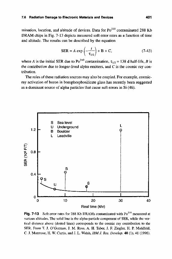
7.6 Radiation Damage to Eiectronic i\/laterials and Devices 401
mination, location, and altitude of devices. Data for Po contaminated 288 Kb DRAM chips in Fig. 7-13 depicts measured soft error rates as a function of time and altitude. The results can be described by the equation
SER = Aexp( ) + B + C, '^1/2 y
(7-43)
where A is the initial SER due to Po^^^ contamination, T1/2 = 138 d half-life, B is the contribution due to longer-lived alpha emitters, and C is the cosmic ray con-tribution.
The roles of these radiation sources may also be coupled. For example, cosmic-ray activation of boron in borophosphosilicate glass has recently been suggested as a dominant source of alpha particles that cause soft errors in Si (46).
% 0.8 h
m CO
0.4 1 -
s
L ^ L
? S
Sea level Underground Boulder Leadville
B 0
J
1
<
S 0
1
L ;>
1 1 10 20
Real time (khr)
30 40
Fig. 7-13 Soft error rates for 288 Kb DRAMs contaminated with Po ° measured at various altitudes. The solid line is the alpha-particle component of SER, while the ver-tical distance above (dotted lines) corresponds to the cosmic ray contribution to the SER. From T. J. O'Gorman, J. M. Ross, A. H. Taber, J. F. Ziegler, H. P. Muhlfeld, C. J. Montrose, H. W. Curtis, and J. L. Walsh, IBM J. Res. Develop, 40 (1), 41 (1996).
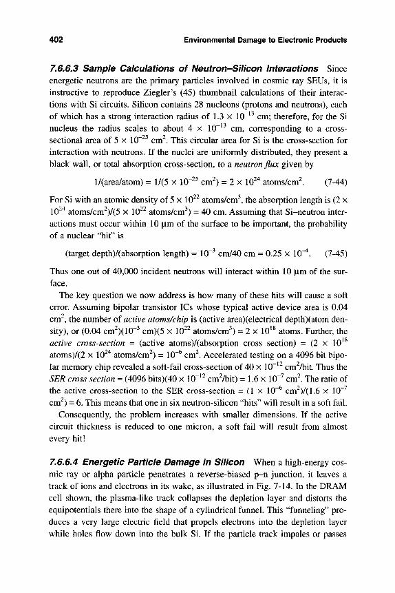
402 Environmental Damage to Electronic Products
7.6.6.3 Sample Calculations of Neutron-Silicon Interactions Since energetic neutrons are the primary particles involved in cosmic ray SEUs, it is instructive to reproduce Ziegler's (45) thumbnail calculations of their interac-tions with Si circuits. Silicon contains 28 nucleons (protons and neutrons), each of which has a strong interaction radius of 1.3 x 10" ^ cm; therefore, for the Si nucleus the radius scales to about 4 x 10" ^ cm, corresponding to a cross-sectional area of 5 x 10" ^ cm^. This circular area for Si is the cross-section for interaction with neutrons. If the nuclei are uniformly distributed, they present a black wall, or total absorption cross-section, to a neutron flux given by
l/(area/atom) = 1/(5 x 10" ^ cm^) = 2 x 10 " atoms/cml (7-44)
For Si with an atomic density of 5 x 10^ atoms/cm^, the absorption length is (2 x 10 atoms/cm )/(5 x 10 atoms/cm ) = 40 cm. Assuming that Si-neutron inter-actions must occur within 10 |im of the surface to be important, the probability of a nuclear "hit" is
(target depth)/(absorption length) = 10"^ cm/40 cm = 0.25 x 10"^. (7-45)
Thus one out of 40,000 incident neutrons will interact within 10 [im of the sur-face.
The key question we now address is how many of these hits will cause a soft error. Assuming bipolar transistor ICs whose typical active device area is 0.04 cm^, the number of active atoms/chip is (active area)(electrical depth)(atom den-sity), or (0.04 cm^)(10"^ cm)(5 x 10^ atoms/cm^) = 2 x 10* atoms. Further, the active cross-section = (active atoms)/(absorption cross section) = (2 x 10 ^ atoms)/(2 x 10 "* atoms/cm^) = 10"^ cm^. Accelerated testing on a 4096 bit bipo-lar memory chip revealed a soft-fail cross-section of 40 x 10" ^ cm^/bit. Thus the SER cross section = (4096 bits)(40 x 10"^^ cm%it) = 1.6 x 10"^ cm^. The ratio of the active cross-section to the SER cross-section = (1 x 10"^ cm^)/(1.6 x 10"^ cm^) = 6. This means that one in six neutron-silicon "hits" will result in a soft fail.
Consequently, the problem increases with smaller dimensions. If the active circuit thickness is reduced to one micron, a soft fail will result from almost every hit!
7.6.6.4 Energetic Particle Damage In Silicon When a high-energy cos-mic ray or alpha particle penetrates a reverse-biased p-n junction, it leaves a track of ions and electrons in its wake, as illustrated in Fig. 7-14. In the DRAM cell shown, the plasma-like track collapses the depletion layer and distorts the equipotentials there into the shape of a cylindrical funnel. This "funneling" pro-duces a very large electric field that propels electrons into the depletion layer while holes flow down into the bulk Si. If the particle track impales or passes
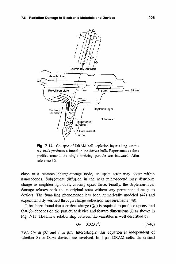
7.6 Radiation Damage to Electronic !\/laterials and Devices 403
- — n Bit line
Substrate
' Hole current
'Funnel
Fig. 7-14 Collapse of DRAM cell depletion layer along cosmic ray track produces a funnel in the device bulk. Representative dose profiles around the single ionizing particle are indicated. After reference 36.
close to a memory charge-storage node, an upset error may occur within nanoseconds. Subsequent diffusion in the next microsecond may distribute charge to neighboring nodes, causing upset there. Finally, the depletion-layer damage relaxes back to its original state without any permanent damage to devices. The funneling phenomenon has been numerically modeled (47) and experimentally verified through charge collection measurements (48).
It has been found that a critical charge (QQ) is required to produce upsets, and that (2c depends on the particular device and feature dimensions (/) as shown in Fig. 7-15. The linear relationship between the variables is well described by
Qc = 0.023 r . (7-46)
with Qc in pC and / in jim. Interestingly, this equation is independent of whether Si or GaAs devices are involved. In 1 |Lim DRAM cells, the critical
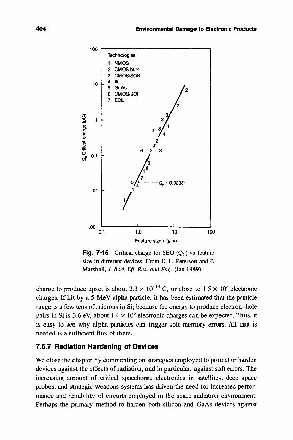
404 Environmental Damage to Electronic Products
100
10
^ 1
CO
o
1 -•IS
•c O 0.1
.01
Technologies
1. NMOS 2. CMOS bulk 3. CMOS/SOS 4. IIL 5. GaAs 6. CMOS/SOI 7. ECL
.001
0.023€2
0.1 1.0 10
Feature size € (jtm)
100
Fig. 7-15 Critical charge for SEU (Qc) vs feature size in different devices. From E. L. Peterson and P. Marshall, J. Rad. Eff. Res. and Eng. (Jan 1989).
charge to produce upset is about 2.3 x 10" "* C, or close to 1.5 x 10^ electronic charges. If hit by a 5 MeV alpha particle, it has been estimated that the particle range is a few tens of microns in Si; because the energy to produce electron-hole pairs in Si is 3.6 eV, about 1.4 x 10^ electronic charges can be expected. Thus, it is easy to see why alpha particles can trigger soft memory errors. All that is needed is a sufficient flux of them.
7.6.7 Radiation Hardening of Devices
We close the chapter by commenting on strategies employed to protect or harden devices against the effects of radiation, and in particular, against soft errors. The increasing amount of critical spacebome electronics in satellites, deep space probes, and strategic weapons systems has driven the need for increased perfor-mance and reliability of circuits employed in the space radiation environment. Perhaps the primary method to harden both silicon and GaAs devices against
Exercises 405
radiation has been through circuit design. This subject is well beyond the scope of this book, but has been reviewed by Kerns and Schafer (49). In the process-ing area a favorite strategy has been to isolate devices from electrical continuity with the base semiconductor wafer. Thus dielectric isolation, or the imposition of an oxide layer or moat around individual MOSFETs or bipolar transistors, has been extensively practiced in silicon technology. Numerous silicon on insulator (SOI) approaches, including growth of Si on sapphire (SOS), separation by ion implantation of oxygen (SIMOX), zone melt recrystallization (ZMR), porous oxidized Si (FIFOS), and epitaxial lateral overgrowth (ELO), have been attempted (35). In general, dielectric isolation has removed latch-up paths and reduced volumes around junctions and oxides where carrier generation and trap-ping can occur.
With respect to soft errors, it is instructive to consider the techniques adopted to minimize their influence in 16 Mb DRAMs subjected to a particles (51). In addition to error-correcting codes, the a particle sensitivity was reduced by the following means:
1. The use of a deep-trench capacitor. Charge stored on this capacitor was designed to be greater than that transferred by three a particles traversing the longest diagonal through the memory-cell volume.
2. Minimizing charge collected by p-n junctions of the MOS transfer device source and drain implants. By fabricating the transfer device in an n-well, charge generated in the substrate is collected by the well supply.
3. Reducing charge collection efficiency by storing memory data "inside" rather than "outside" the dielectrically isolated storage trench. In the latter, charge is col-lected over a larger potential substrate volume and source of radioactive atoms.
EXERCISES
7-1 An electronic vacuum tube 20 cm^ in volume is pumped to 10" ^ atm prior to glass-metal sealing. For a moisture penetration rate of 1 x 10"^ atm-cm^/s, how long will it take for the pressure in the tube to rise an order of magnitude?
7-2 The mean time to failure of plastic packages as a function of temperature and relative humidity is given by MTTF = i?(RH)"" exp [EJkT], where B is a constant. a. If n = 2.66 and E^ = 0.79 eV does a 10% increase in relative humidity
have a greater effect in reducing mean life than a 10% increase in tem-perature?
406 Environmental Damage to Electronic Products
b. For relative humidity and temperature variables to have an equal influ-ence in degrading plastic packages, as measured by MTTF, what rela-tionship must connect RH, T, n and E^l
7-3 An aluminum contact film that is 1 |xm thick and 0.1 mm x 0.1 mm in area carries a current of 1 |xA. Under a worst-case corrosion scenario how long would it take the metal to be totally converted into ions?
7-4 Write possible balanced chemical reactions for the formation of NiCl2 and NiCOs corrosion products when Ni is exposed to the atmosphere and water containing chlorides.
7-5 a. Is "purple plague" formation likely to occur during aqueous corrosion of a gold-wire bond to an aluminum contact pad?
b. Suppose a condensed moisture layer containing a 10"^ molar concen-tration of Ar^ surrounds the pad, while a 10"^ molar concentration of Au" ^ coats the wire. What maximum potential can develop between these metals? What minimum potential can develop?
7-6 It has been claimed that the AU4AI intermetallic compound corrodes in the presence of bromine ions according the reaction AU4AI + 3Br~ -^ 4Au + AlBr3 -I- 3e~. Suggest a subsequent reaction that regenerates bromine ions. What evidence is there that such a reaction sequence occurs?
7-7 The contact metal WSi2 is subject to electrolytic corrosion in the presence of moisture and voltage bias. Write a chemical reaction that would tend to convert this conducting silicide to insulating oxide byproducts. If the corresponding free energies of formation (AG) from elements at 298K are AG(WSi2) = -22 kcal/mol, AGCWOa) = -204 kcal/mol, and AG(Si02) = -182 kcal/mol, what is the overall free energy change of the corrosion reaction? Note: You may have to consult a table of thermodynamic data.
7-8 The use of aluminum electrical wiring in the home has been known to cause fires that apparently initiate at plug outlets; in contrast, copper wiring appears to be immune from this problem. Give a possible reason for these observations.
7-9 Suppose corrosion of metal within a plastic package occurs by moisture per-meation followed by a chemical reaction described by second-order kinetics such that dC/dt = -k(C-Co)^ where k is the rate constant. Derive an expres-sion for the reliability function.
7-10 What similarities and differences in matrix environment, mass-transport mechanisms, current densities, damage morphology, temperature depen-
References 407
dence, and degradation kinetics exist between wet migration and solid-state electromigration?
7-11 During electrolytic refining of copper, the impure-anode sheet metal is plated onto pure Cu cathodes in cells that employ aqueous CUSO4 elec-trolytes. In this process, as with wet metal migration, dendrites often span the anode-cathode spacing and short the electrodes. Suggest reasons why the formation of dendrites is so heterogeneous and why they grow with such variable velocity. In the case of copper refining, what practical mea-sures can be taken to minimize cell shorting by dendrites?
7-12 The 100 nm thick Si02 film of a capacitor was uniformly contaminated with a concentration of 1 x 10^^ sodium ions/cm^. Application of 5 volts swept all of the sodium to the negative electrode. a. How long does it take Na" ions to electromigrate across the oxide at 300K? b. The voltage is reduced to zero. Sketch resultant time-dependent con-
centration profiles of Na" as a function of time. c. How long will it take the Na" to diffuse back across the oxide?
7-13 As a result of exposure to radiation: a. Metals harden but become less ductile and suffer damage in the form of
creep, void swelling, and hydrogen embrittlement. b. Ceramics undergo color changes and exhibit loss of thermal conductiv-
ity but enhancement of electrical conductivity. c. Polymers generally lose strength and ductility, discolor, and evolve gas
(e.g., hydrogen). Select one of these material classes and write a report explaining reasons for the radiation-damage effects manifested. (The April 1997 issue of the MRS Bulletin is devoted to materials performance in radiation fields.)
7-14 How many electron-hole pairs are created in Si and GaAs by exposing each to a radiation dose of 1 Gy?
7-15 Nuclei of Th^^^ have an activity of 1.1 x 10"^ Ci/g and release 6 alpha par-ticles per disintegration when they decay to Pb^^ . If these alpha particles can penetrate 50|im of Si, what aP flux can be expected?
7-16 A source of neutrons impinges on both silicon and germanium. What ratio of subsurface interaction depths will enable the probability of neutron-Ge atom hits to equal the number of neutron-Si atom hits?
7-17 Soft-error fail rates per chip in 288 Kb DRAMS (1986) were measured to be approximately 1 fail per year. More recent data for 4 Mb DRAM (1993)
408 Environmental Damage to Electronic Products
memory chips from different manufacturers reveal SER values of 0.0026 to 0.00046 fails per year. a. Suggest possible reasons for the differences in these values. b. How many FITS does 0.00046 fails per year correspond to?
7-18 A 64 Mb bipolar cache memory chip containing 5 x 10^ bits in the mem-ory is exposed to an energetic nucleon flux equal to 10^/cm^-yr. The prob-ability of a soft error is given in terms of the cross-section, which has a value of 4 x 10"^^ cm^i t . How many soft errors can be expected if this chip operates for a year?
REFERENCES
1. R. B. Comizzoli, R. R Frankenthal, R. E. Lobnig, G. A. Peins, L. A. Psota-Kelty, D. J. Siconolfi, and D. J. Sinclair, The Electrochem. Soc. Interface 26, Fall (1993).
2. D. J. Schneider and D. C. WiUiams, Lasers and Optronics 25, Oct. (1994). 3. J. D. Guttenplan, ASM Handbook, Vol. 13, 1107 (1987). 4. E. White, G. Slenski and B. Dobbs, ASM Handbook, Vol. 13, 1113 (1987). 5. M. Pecht, IEEE Trans, on Components, Hybrids and Manuf. Tech. 11(3),
383 (1990). 6. R. P. Merrett, Tutorial Notes, IEEE International Reliability Physics Sympo-
sium, 1-2.1 (1984). 7. A. Roth, Vacuum Technology, North-Holland, Amsterdam (1976). 8. D. A. Jones, Principles and Prevention of Corrosion, Macmillan, New York
(1992). 9. M. G. Fontana, Corrosion Engineering, 3rd ed., McGraw Hill, New York
(1978). 10. M. Tullmin and R R. Roberge, IEEE Trans, on Reliability 44, 271 (1995). 11. X. Shan and M. Pecht, in Thermal Stress and Strain in Microelectronics
Packaging, ed. J. H. Lau, van Nostrand Reinhold, New York (1993). 12. G. L. Schnable, R. B. Comizzoh, W. Kern, and L. K. White, RCA Review
40, 416 (1979). 13. D. S. Peck, 24th Annual Proceedings of the IEEE Reliability Physics Sym-
posium, p. 44 (1986). 14. M. lannuzzi, IEEE Trans, on Components, Hybrids and Manuf. Tech.,
CHMT-6, 181 (1983).
References 409
15. P. Totta, J. Vac. Sci. Tech 13, 26 (1976). 16. S. Thomas and H. M. Berg, 23th Annual Proceedings of the IEEE Reliabil-
ity Physics Symposium, p. 153 (1985). 17. A. J. Griffen, S. E. Hema'ndez, F. R. Brotzen, J. D. Lawrence, J. W.
McPherson, and C. F. Dunn, 31st Annual Proceedings of the IEEE Reliabil-ity Physics Symposium, p. 327 (1993).
18. K. H. Ritz, W. I. Stacy, and E. K. Broadbent, 25th Annual Proceedings of the IEEE Reliability Physics Symposium, p. 28, (1987).
19. W. T. Anderson and A. Christou, IEEE Trans, on Reliability, R-29, 222 (1980).
20. R. S. Torkington and D. Lamoreaux, ASM International Symposium for Testing and Failure Analysis (ISTFA), p. 225 (1990)
21. J. M. E. Harper, E. G. Colgan, C.-K. Hu, J. R Hummel, L. P. Buchwalter, and C. E. Uzoh. MRS Bulletiri, XIX (8), 23 (1994).
22. S. J. Krumbein, IEEE Trans, on Reliability 44 (4), 539 (1995). 23. T. Saigusa, T. Ohtaki, M. Nakajima, and Y. Nakao, Materials Developments
in Microelectronic Packaging Conf Proc, Quebec, Canada, p. 345, Aug (1991).
24. M. Pecht, IEEE Trans, on Components, Hybrids and Manuf Tech. 13, 383 (1990).
25. B. Rudra and D. Jennings, IEEE Trans, on Reliability 43, 354 (1994). 26. G. T. Kohman, H. W. Hermance, and G. H. Downes, Bell Syst. Tech J.
XXXIV, No. 6, 1115 (1955). 27. J. J. Steppan, J. A. Roth, L. C. Hall, D. A. Jeanotte, arid S.P. Carbone, J.
Electrochem. Soc. 134 (1), 175 (1987). 28. G. DiGiacomo, in Microelectronics Manufacturing Diagnostics Handbook,
ed. A. H. Landzberg, Van Nostrand Reinhold, New York (1993). 29. M. Ohring, The Materials Science of Thin Films, Acadermc Press, Boston
(1992). 30. R. T. Howard, IEEE Trans, on Components, Hybrids and Manuf. Tech.
CHMT-4, 520(1981). 31. Handbook of Chem and Physics, 59th Edition, CRC Press, Cleveland
(1978-79). 32. R. L. Hance, J. W. Miller, K. B. Erington, and M. A. Chonko, Tutorial
Notes, IEEE International Reliability Physics Symposium, 4.1 (1995). 33. H. Hughes in T. P. Ma, and P. V Dressendorfer, eds.. Ionizing Radiation
Effects in MOS Devices and Circuits, J. Wiley and Sons, New York (1989). 34. T. P. Ma and P. V. Dressendorfer, eds.. Ionizing Radiation Effects in MOS
Devices and Circuits, J. Wiley and Sons, New York (1989).
410 Environmental Damage to Electronic Products
35. A. Holmes-Siedle and L. Adams, Handbook of Radiation Effects, Oxford University Press, Oxford (1993).
36. G. C. Messenger and M. S. Ash, The Effects of Radiation on Electronic Sys-tems, 2nd ed.. Van Nostrand Reinhold, New York (1992).
37. J. R. Srour and J. M. McGarrity, Pwc. IEEE 76, 1443 (1988). 38. K. F. Galloway and R. D. Schrimpf, Microelectronics Journal. 21, 67
(1990). 39. G. J. Papaioannou, in A. Christou and B. A. Unger, eds., Semiconductor
Device Reliability, Kluwer, Amsterdam (1990). 40. L. Adams, Microelectronics Journal 16, 17 (1985). 41. J. F. Ziegler and G. R. Srinivasan, eds., IBM J. Res. and Develop. 40 (1)
(1996). 42. T. C. May and M. H. Woods, IEEE Trans, on Electron Devices, ED-26, 2
(1979). 43. J. F. Ziegler and W. A. Lanford, Science 206, 776 (1979). 44. L. Lantz, IEEE Trans on Reliability 45 (2), 174 (1996). 45. J. F Ziegler, IBM J Res. and Develop. 40 (1), 19 (1996). 46. R. Baumann, T. Hossain, S. Murata, and H. Kitagawa, 33rd Annual Pro-
ceedings of the IEEE Reliability Physics Symposium, p. 296 (1995). 47. H. L. Grubin, J. R Kreskovsky, and B. C. Weinberg, IEEE Trans on Nuclear
Science, NS-31, 1161(1984). 48. G. C. Messinger, IEEE Trans on Nuclear Science, NS-29, 2024 (1982). 49. S. E. Kerns and B. D. Shafer, Proc. IEEE 76, 1470 (1988). 50. C. H. Stapper and W. A. Klassen, 30th Annual Proceedings of the IEEE
Reliability Physics Symposium, p. 3 (1992).
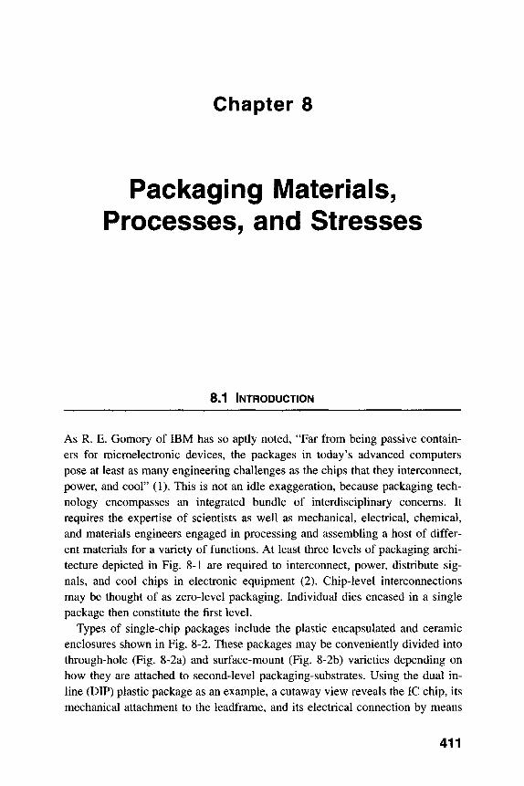
Chapter 8
Packaging Materials, Processes, and Stresses
8.t INTRODUCTION
As R. E. Gomory of IBM has so aptly noted, "Far from being passive contain-ers for microelectronic devices, the packages in today's advanced computers pose at least as many engineering challenges as the chips that they interconnect, power, and cool" (1). This is not an idle exaggeration, because packaging tech-nology encompasses an integrated bundle of interdisciplinary concerns. It requires the expertise of scientists as well as mechanical, electrical, chemical, and materials engineers engaged in processing and assembling a host of differ-ent materials for a variety of functions. At least three levels of packaging archi-tecture depicted in Fig. 8-1 are required to interconnect, power, distribute sig-nals, and cool chips in electronic equipment (2). Chip-level interconnections may be thought of as zero-level packaging. Individual dies encased in a single package then constitute the first level.
Types of single-chip packages include the plastic encapsulated and ceramic enclosures shown in Fig. 8-2. These packages may be conveniently divided into through-hole (Fig. 8-2a) and surface-mount (Fig. 8-2b) varieties depending on how they are attached to second-level packaging-substrates. Using the dual in-line (DIP) plastic package as an example, a cutaway view reveals the IC chip, its mechanical attachment to the leadframe, and its electrical connection by means
411
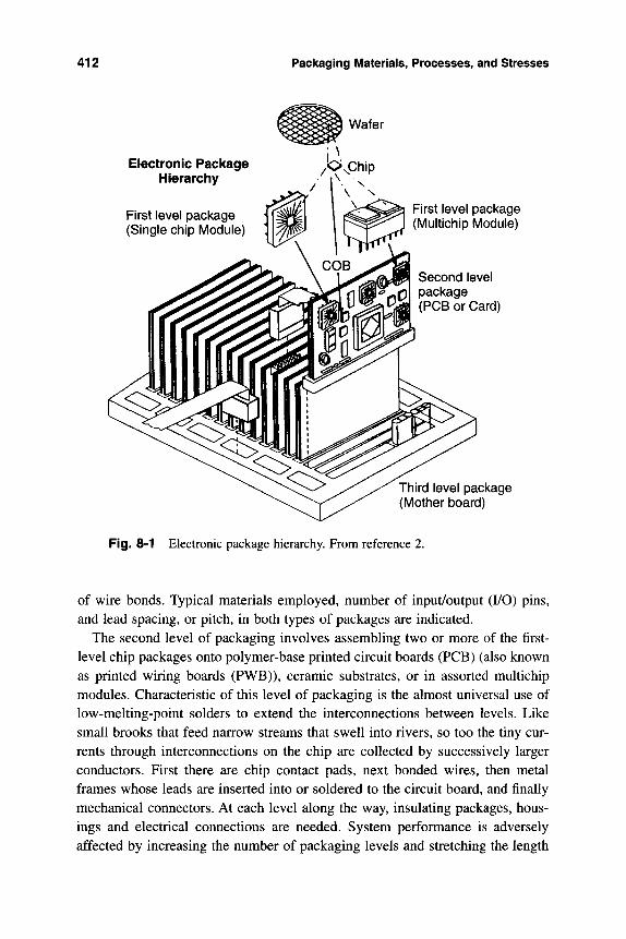
412 Packaging Materials, Processes, and Stresses
Wafer
Electronic Package Hierarchy
First level package (Single chip Module)
First level package (Multichip Module)
Second level package (PCB or Card)
Third level package (Mother board)
Fig. 8-1 Electronic package hierarchy. From reference 2.
of wire bonds. Typical materials employed, number of input/output (I/O) pins, and lead spacing, or pitch, in both types of packages are indicated.
The second level of packaging involves assembling two or more of the first-level chip packages onto polymer-base printed circuit boards (PCB) (also known as printed wiring boards (PWB)), ceramic substrates, or in assorted multichip modules. Characteristic of this level of packaging is the almost universal use of low-melting-point solders to extend the interconnections between levels. Like small brooks that feed narrow streams that swell into rivers, so too the tiny cur-rents through interconnections on the chip are collected by successively larger conductors. First there are chip contact pads, next bonded wires, then metal frames whose leads are inserted into or soldered to the circuit board, and finally mechanical connectors. At each level along the way, insulating packages, hous-ings and electrical connections are needed. System performance is adversely affected by increasing the number of packaging levels and stretching the length
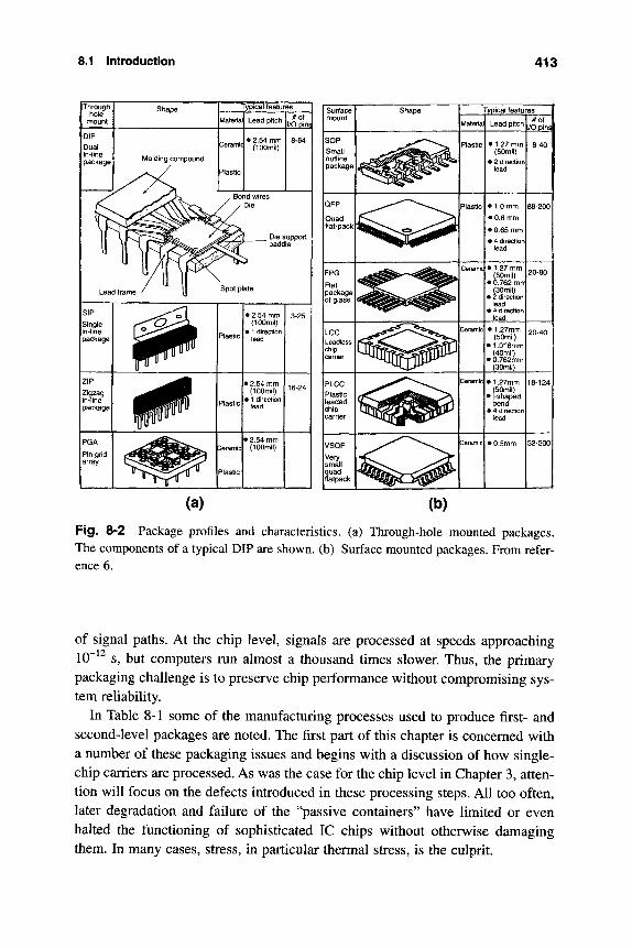
8.1 Introduction 413
Surface mount
SOP Small outline package!
Quad flat-pack
Flat package of glass
Leadless chip carrier
PLCC Plastic leaded I chip carrier
|VSQF
Very small quad flatpack
Typical features
Material Lead pitch #of t /0 pind
• 1.27 mm (50mil)
• 2 direction] lead
• 1.0 mm
• 0.8 mm
• 0.65 mm
• 4 direction! lead
• 1.27 mm (SOmil)
• 0.762 mnr| (30mil)
• 2 direction lead
• 4 direction lead
• 1.27mm (SOmil)
• 1.016mm (40mil)
• 0.762mm (SOmil)
• 1.27mm (SOmil)
• j-shaped bend
• 4 direction] lead
(b)
Fig. 8-2 Package profiles and characteristics, (a) Through-hole mounted packages. The components of a typical DIP are shown, (b) Surface mounted packages. From refer-ence 6.
of signal paths. At the chip level, signals are processed at speeds approaching 10~ s, but computers run almost a thousand times slower. Thus, the primary packaging challenge is to preserve chip performance without compromising sys-tem reliability.
In Table 8-1 some of the manufacturing processes used to produce first- and second-level packages are noted. The first part of this chapter is concerned with a number of these packaging issues and begins with a discussion of how single-chip carriers are processed. As was the case for the chip level in Chapter 3, atten-tion will focus on the defects introduced in these processing steps. All too often, later degradation and failure of the "passive containers" have limited or even halted the functioning of sophisticated IC chips without otherwise damaging them. In many cases, stress, in particular thermal stress, is the culprit.
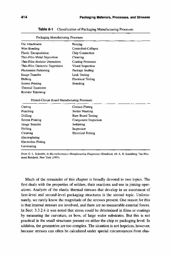
414 Packaging Materials, Processes, and Stresses
Table 8-1 Classification of Packaging Manufacturing Processes
Packaging Manufacturing Processes
Die Attachment Brazing Wire Bonding Controlled-CoUapse Plastic Encapsulation Chip Connection Thin-Film Metal Deposition Cleaning Thin-Film Resistor Deposition Coating Processes Thin-Film Dielectric Deposition Visual Inspection Photoresist Patterning Package Sealing Image Transfer Leak Testing Etching Electrical Testing Screen Printing Branding Thermal Treatment Resistor Trimming
Printed-Circuit Board Manufacturing Processes
Cutting Contact Plating Punching Solder Masking DriUing Bare Board Testing Screen Printing Component Inspection Image Transfer Soldering Etching Inspection Cleaning Electrical Testing Electroplating Electroless Plating Laminating
From G. L. Schnable, in Microelectronics Manufacturing Diagnostics Handbook, ed. A. H. Landsberg, Van Nos-trand Reinhold, New York (1993).
Much of the remainder of this chapter is broadly devoted to two topics. The first deals with the properties of solders, their reactions and use in joining oper-ations. Analysis of the elastic thermal stresses that develop in an assortment of first-level and second-level packaging structures is the second topic. Unfortu-nately, we rarely know the magnitude of the stresses present. One reason for this is that internal stresses are involved, and there are no measurable extemal forces. In Sect. 3.3.2.4 it was noted that stress could be determined in films or coatings by measuring the curvature, or bow, of large wafer substrates. But this is not practical in the small structures present on either the chip or packaging level. In addition, the geometries are too complex. The situation is not hopeless, however, because stresses can often be calculated under special circumstances from elas-
8.2 IC Chip-Packaging Processes and Effects 415
ticity theory or determined using finite-element methods. Occasionally, the ther-mal stress levels are high enough to induce degradation of packaging materials and plastic deformation of solder joints that causes them to fail by creep and thermal fatigue. These latter time-dependent failure mechanisms and associated reliability issues will be addressed in Chapter 9.
Many of the above and related packaging issues are treated in a growing num-ber of edited handbooks and texts (1-9). Readers requiring a more detailed knowledge of the engineering analysis and design, materials selection, cooling, and reliability of electronic packaging materials and structures should consult them.
8.2 IC CHtP-PACKAGING PROCESSES AND EFFECTS
8.2.1 Scope
By the time the final step of chip processing has been completed, some wafers are worth a few hundred times their weight in gold. However, fabrication of the wafer does not necessarily mean that we have a finished product. Only when the chip is tested and safely enclosed within one of the packages of Fig. 8-2 is this phase of manufacturing completed. These packaging and assembly steps, schematically outlined in Fig. 8-3, are fraught with processing pitfalls that can seriously limit yield. Wafers produced with such great care and cost must now be separated into chips or dies, interconnected, and packaged. There is a great contrast between processing at the chip and package levels, the defects created and the reliability implications involved. Distinguishing features worth noting include the following:
1. Size If ~ 1 |jLm or less is the characteristic process feature size on chips, tens to thousands of |xm and larger are typical packaging-component dimensions.
2. Materials Packaging materials and structures are chosen to meet the demands of ICs. Thus metals are selected according to how well they conduct current into and out of chips, and encapsulants on their ability to encase and pro-tect the precious chip. A wider spectrum of materials is employed in packages than in chips. In addition to solely electrical conduction functions, metals are used in packages as mechanical supports, to conduct heat away (heat sinks), and to seal the contents. Ceramics like alumina also serve as containers for chips and are often the substrates for mounting semiconductor chips. Polymers are employed to hermetically encase the chips and are the substance of printed cir-cuit boards. Even silicon is used as a substrate in the silicon-on-silicon multi-
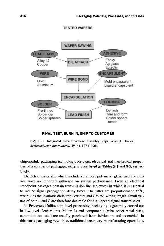
416 Packaging Materials, Processes, and Stresses
TESTED WAFERS
Gold Aluminium
Pre-tinned Solder dip Solder spheres
Mold encapsulent Liquid encapsulent
Deflash Trim and form Solder sphere attach
FINAL TEST, BURN IN, SHIP TO CUSTOMER
Fig. 8-3 Integrated circuit package assembly steps. After C. Bauer, Semiconductor International 19 (4), 127 (1996).
chip-module packaging technology. Relevant electrical and mechanical proper-ties of a number of packaging materials are listed in Tables 2-1 and 8-2, respec-tively.
Dielectric materials, which include ceramics, polymers, glass, and compos-ites, have an important influence on system performance. From an electrical standpoint packages contain transmission line structures in which it is essential to reduce signal propagation delay times. The latter are proportional to e ^ L, where £ is the insulator dielectric constant and L is the wiring length. Small val-ues of both 8 and L are therefore desirable for high-speed signal transmission.
3. Processes Unlike chip-level processing, packaging is generally carried out in low-level clean rooms. Materials and components (wire, sheet metal parts, ceramic plates, etc.) are usually purchased from fabricators and assembled. In this sense packaging resembles traditional secondary-manufacturing operations.
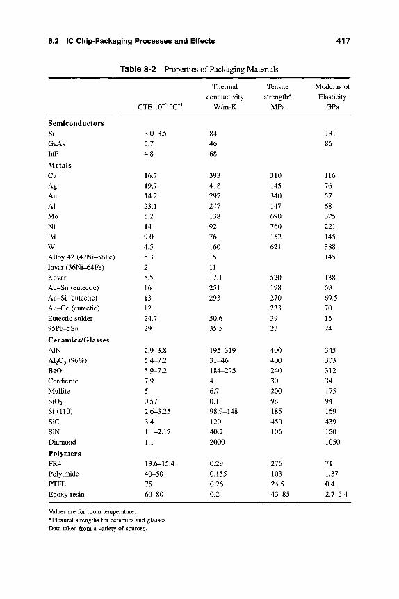
8.2 IC Chip-Packaging Processes and Effects 417
Table 8-2 Properties of Packaging Materials
Semiconductors Si GaAs In?
Metals Cu
Ag Au Al Mo Ni Pd W Alloy 42 (42Ni-58Fe) Invar (36Ni-64Fe) Kovar Au-Sn (eutectic) Au-Si (eutectic) Au-Ge (eutectic) Eutectic solder 95Pb-5Sn
Ceramics/Glasses AIN AI2O3 (96%) BeO Cordierite MuUite
Si02 Si (110) SiC SiN Diamond
Polymers FR4 Polyimide PTFE Epoxy resin
CTE 10"^ °C"^
3.0-3.5 5.7 4.8
16.7 19.7 14.2 23.1 5.2 14 9.0 4.5 5.3 2 5.5 16 13 12 24.7 29
2.9-3.8 5.4-7.2 5.9-7.2 7.9 5 0.57 2.6-3.25 3.4 1.1-2.17 1.1
13.6-15.4 40-50 75 60-80
Thermal conductivity
W/m-K
84 46 68
393 418 297 247 138 92 76 160 15 11 17.1 251 293
50.6 35.5
195-319 31-46 184-275 4 6.7 0.1 98.9-148 120 40.2 2000
0.29 0.155 0.26 0.2
Tensile strength*
MPa
310 145 340 147 690 760 152 621
520 198 270 233 39 23
400 400 240 30 200 98 185 450 106
276 103 24.5 43-85
Modulus of Elasticity
GPa
131 86
116 76 57 68 325 221 145 388 145
138 69 69.5 70 15 24
345 303 312 34
175 94 169 439 150 1050
71 1.37 0.4 2.7-3.4
Values are for room temperature. *Flexural strengths for ceramics and glasses Data taken from a variety of sources.
418 Packaging Materials, Processes, and Stresses
Molding of polymers, soldering, joining, and bonding are important packaging processes.
4. Processing Temperatures Compared to chip-level processing, tempera-tures employed in packaging are relatively low. Instead of 1000°C and above during epitaxy, diffusion, and especially during crystal growth, eutectic die-attach processes only reach -'425°C. Other than die attachment, packaging mate-rials rarely experience temperatures above a few hundred degrees C. Note that these comments refer only to processes where the IC chip is present; excluded are prior processing of components, e.g, firing glass or ceramic-metal hermetic seals and conductive inks in hybrid circuits.
5. Defects and Reliability Instead of crystallographic and other microscopic defects on the chip level, packaging defects are macroscopic in size. They con-sist, for example, of voids in polymers and die-attach materials, and cracks in chips, dies, and solders. Packaging failures often stem from thermal-stress effects, but environmental damage due to corrosion and humidity is not uncom-mon. A compilation of defects arising from package manufacturing is Usted in Table 8-3.
Although this table specifically targets the reliability of IC packages, very similar issues arise in the packaging of related electronic products. For example, Fig. 8-4 depicts the reliability concerns in a micromachined-silicon pressure sen-sor and its associated package. Fabrication of the miniature mechanical sensor borrows heavily from silicon lithography and processing technology to create the diaphragm and associated electrical connections.
We now briefly survey some of the important first-level packaging processes in a descriptive way, emphasizing some of the defects introduced and reliability issues raised along the way.
8.2.2 First-Level Electrical Interconnection
8.2.2.1 Die Attachment The first step in the packaging process is scribing and breaking the wafer into dies. As noted in Sect. 3.3.2, even this step can be troublesome by producing serious losses due to die cracking. Next, the die is bonded to a conducting paddle or substrate that is mechanically strong and makes provision for electrical connection to subsequent packaging levels. Sheet metal (e.g., Cu, alloy 42 (42Ni/58Fe), alloy 50 (50Ni/50Fe) lead (pronounced "leed") frames, metallized ceramic (AI2O3, AIN) plates, and even Si wafers have served as substrates in different packaging technologies. Most commonly, how-ever, metals are the substrates. The Si chip is bonded to them either by means of Pb-5 wt.%Sn and more popularly, by Au-Si eutectic alloy solders, or by metal (Ag)-filled conductive organic and glass adhesives. In eutectic bonding, a thin
Table 8-3 Defects Associated with Packaging Manufacturing Processes
A. Chip Packaging
Die Bonding AlkaU ion contamination; Chip fracture; Epoxy creep; Excessive electrical resistance; Excessive
moisture source; Excessive thermal resistance; Halide contamination; Horizontal chip cracks; Inad-
equate bond area; Incorrect bond-line thickness; Incorrect die selection; Incorrect positioning; Ionic contamination; Lead frame oxidation; Low die shear; Mechanical damage to chip; Non-wetting; Outgassing source; Poor adhesion; Poor flow of adhesive; Poor wetting; Resin bleed; Silver migra-tion; Source of particles; Stress effects; Too little or too much adhesive; Vertical chip cracks; Voids; Wrong alloy. Wire bonding Chip scratches; Chip fracture; Contamination; Cratering; Incorrect wire dress; Incorrect bond placement; loose particles; low bond strength; Overbonding; Purple plague; Smeared metallization; Substrate metal too hard; Underbonding; Wire too hard or too soft. Plastic encapsulation Cracks; Damage by filler particles; Excessive cure; Excessive flash; Excessive source of alpha par-ticles; Excessive coefficient of thermal expansion (CTE) mismatch; Inadequate cure; Inadequate moisture resistance; Inadequate plastic flow; Inadequate thermal conductivity; Ionic contamination; PoOT adhesion to lead frame; Voids; Wire sweep. Screen printing Cracks; Excessive amount of screened paste; Excessive bleed; Excessive pinholes; Inadequate amount of screened paste; Missing features; Poor adhesion; Poor alignment; Poor resolution. Package sealing
Cavitation; Contamination; Deformed metallization; Excessive deformation; Excessive moisture in package; Excessively high leak rate; Lack of hermeticity; Loose particles; Mechanical damage; Oxide cracks in multilevel metallized ICs; Passivation cracks; Poor wetting; Weld splash; Wrong ambient. Cleaning
Electrostatic discharge (ESD) effects; Inadequate removal of surface impurities; Ionic contamina-tion; Organic residues; Particulate contamination; Radiation damage to semiconductor devices; Surface pitting.
Controlled-collapse chip connection Bridging; Dewetting; Flux residues; Incorrect final spacing; Poor reflow; Poor solder wetting; Too little or too much lead; Too little or too much tin;
B. Printed-Circuit Board Manufacturing Processes
Drilling Burrs; Debris; Delamination; Drill wander; Extra holes; Foreign matter in holes; Holes not drilled through; Loose fibers; Mechanical damage; Misregistered holes; Missing holes; Nailheading; Oblong holes; Plowing; Rifling; Smears; Voids; Wrong size holes.
Electroplating Burning; Edge feathers; Grainy deposits; Inadequate substrate preparation; Poor adhesion; Poor reflow; Poor throwing power; Roughness; Treeing; Whiskers; Wrong alloy composition; Wrong thickness.
Soldering See Table 8-6.
From G. L. Schnable, in Microelectronics Manufacturing Diagnostics Handbook, ed. A. H. Landsberg, Van Nos-trand Reinhold, New York (1993).
419
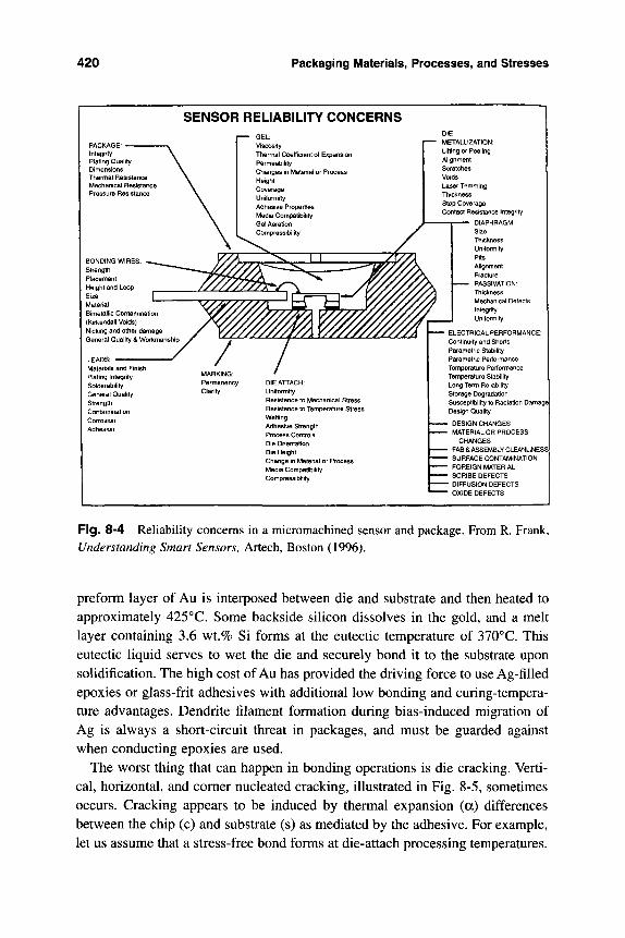
420 Packaging Materials, Processes, and Stresses
SENSOR RELIABILITY CONCERNS
PACKAGE: • Integrity Plating Quality Dimensions Thermal Resistance Mechanical Resistance Pressure Resistance
BONDING WIRES: Strength Placement Height and Loop Size Material Bimetallic Contamination (Kirkendall Voids) Nicking and other damage General Quality & Workmanship
GEL: Viscosity Thermal Coefficient of Expansion Permeability Changes in Material or Process Height Coverage Unifomiity Adhesive Properties Media Compatibility Gel Aeration Compressibility
LEADS: — — Materials and Finish Plating Integrity Solderability General Quality Strength Contamination Corrosion Adhesion
DIE ATTACH: Uniformity Resistance to Mechanical Stress Resistance to Temperature Stress Wetting Adhesive Strength Process Controls Die Orientation Die Height Change in Material or Process Media Compatibility Compressibility
DIE METALLIZATION: Lifting or Peeling Alignment Scratches Voids Laser Trimming Thickness Step Coverage Contact Resistance Integrity
DIAPHRAGM: Size Thickness Uniformity Pits Alignment Fracture PASSIVATION: Thickness Mechanical Defects Integrity Uniformity
• ELECTRICAL PERFORMANCE: Continuity and Shorts Parametric Stability Parametric Performance Temperature Performance Temperature Stability Long Term Reliability Storage Degradation Susceptibility to Radiation Damage] Design Quality
- DESIGN CHANGES - MATERIAL OR PROCESS
CHANGES - FAB & ASSEMBLY CLEANLINESS] - SURFACE CONTAMINATION - FOREIGN MATERIAL - SCRIBE DEFECTS - DIFFUSION DEFECTS - OXIDE DEFECTS
Fig. 8-4 Reliability concerns in a micromachined sensor and package. From R. Frank, Understanding Smart Sensors, Artech, Boston (1996).
preform layer of Au is interposed between die and substrate and then heated to approximately 425°C. Some backside silicon dissolves in the gold, and a melt layer containing 3.6 wt.% Si forms at the eutectic temperature of 370°C. This eutectic liquid serves to wet the die and securely bond it to the substrate upon solidification. The high cost of Au has provided the driving force to use Ag-filled epoxies or glass-frit adhesives with additional low bonding and curing-tempera-ture advantages. Dendrite filament formation during bias-induced migration of Ag is always a short-circuit threat in packages, and must be guarded against when conducting epoxies are used.
The worst thing that can happen in bonding operations is die cracking. Verti-cal, horizontal, and comer nucleated cracking, illustrated in Fig. 8-5, sometimes occurs. Cracking appears to be induced by thermal expansion (a) differences between the chip (c) and substrate (s) as mediated by the adhesive. For example, let us assume that a stress-free bond forms at die-attach processing temperatures.
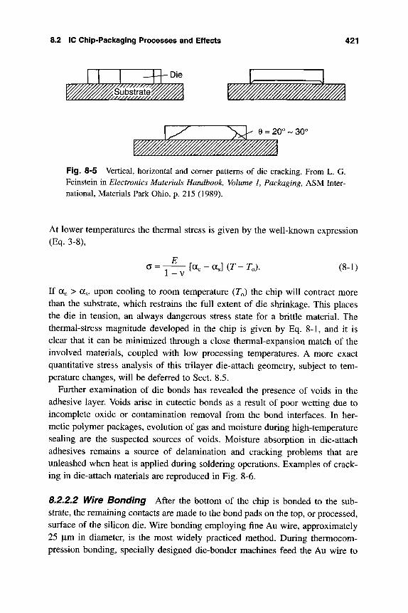
8.2 IC Chip-Packaging Processes and Effects 421
m
e = 20° - 30°
Fig. 8-5 Vertical, horizontal and comer patterns of die cracking. From L. G. Feinstein in Electronics Materials Handbook, Volume 1, Packaging, ASM Inter-national, Materials Park Ohio, p. 215 (1989).
At lower temperatures the thermal stress is given by the well-known expression (Eq. 3-8),
a = 1 - v [ a e - a J C r - T o ) . (8-1)
If ttc > as, upon cooling to room temperature {T^ the chip will contract more than the substrate, which restrains the full extent of die shrinkage. This places the die in tension, an always dangerous stress state for a brittle material. The thermal-stress magnitude developed in the chip is given by Eq. 8-1, and it is clear that it can be minimized through a close thermal-expansion match of the involved materials, coupled with low processing temperatures. A more exact quantitative stress analysis of this trilayer die-attach geometry, subject to tem-perature changes, will be deferred to Sect. 8.5.
Further examination of die bonds has revealed the presence of voids in the adhesive layer. Voids arise in eutectic bonds as a result of poor wetting due to incomplete oxide or contamination removal from the bond interfaces. In her-metic polymer packages, evolution of gas and moisture during high-temperature sealing are the suspected sources of voids. Moisture absorption in die-attach adhesives remains a source of delamination and cracking problems that are unleashed when heat is applied during soldering operations. Examples of crack-ing in die-attach materials are reproduced in Fig. 8-6.
8.2.2.2 Wire Bonding After the bottom of the chip is bonded to the sub-strate, the remaining contacts are made to the bond pads on the top, or processed, surface of the silicon die. Wire bonding employing fine Au wire, approximately 25 |im in diameter, is the most widely practiced method. During thermocom-pression bonding, specially designed die-bonder machines feed the Au wire to
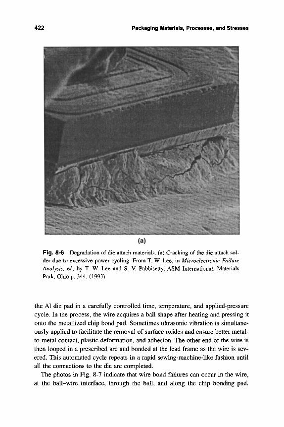
422 Packaging Materials, Processes, and Stresses
Fig. 8-6 Degradation of die attach materials, (a) Cracking of the die attach sol-der due to excessive power cycling. From T. W. Lee, in Microelectronic Failure Analysis, ed. by T. W. Lee and S. V. Pabbisetty, ASM International, Materials Park, Ohio p. 344, (1993).
the Al die pad in a carefully controlled time, temperature, and applied-pressure cycle. In the process, the wire acquires a ball shape after heating and pressing it onto the metallized chip bond pad. Sometimes ultrasonic vibration is simultane-ously applied to facilitate the removal of surface oxides and ensure better metal-to-metal contact, plastic deformation, and adhesion. The other end of the wire is then looped in a prescribed arc and bonded at the lead frame as the wire is sev-ered. This automated cycle repeats in a rapid sewing-machine-like fashion until all the connections to the die are completed.
The photos in Fig. 8-7 indicate that wire bond failures can occur in the wire, at the ball-wire interface, through the ball, and along the chip bonding pad.
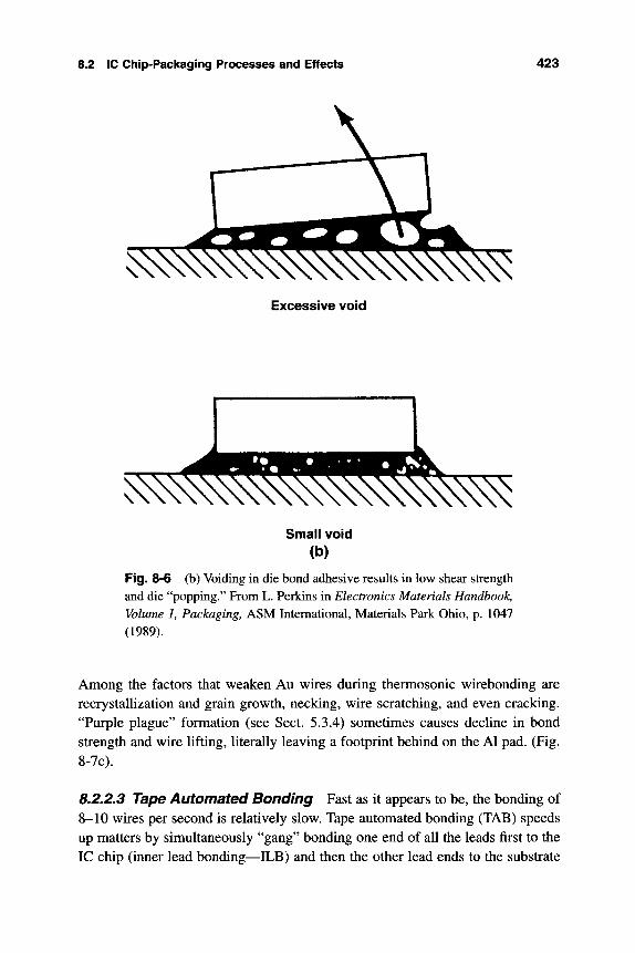
8.2 IC Chip-Packaging Processes and Effects 423
5 ^ ^ Excessive void
v ^ ^ ^
Small void (b)
Fig. 8-6 (b) Voiding in die bond adhesive results in low shear strength and die "popping." From L. Perkins in Electronics Materials Handbook, Volume 1, Packaging, ASM International, Materials Park Ohio, p. 1047 (1989).
Among the factors that weaken Au wires during thermosonic wirebonding are recrystallization and grain growth, necking, wire scratching, and even cracking. "Purple plague" formation (see Sect. 5.3.4) sometimes causes decline in bond strength and wire lifting, literally leaving a footprint behind on the Al pad. (Fig. 8-7c).
8.2.2.3 Tape Automated Bonding Fast as it appears to be, the bonding of 8-10 wires per second is relatively slow. Tape automated bonding (TAB) speeds up matters by simultaneously "gang" bonding one end of all the leads first to the IC chip (inner lead bonding—ILB) and then the other lead ends to the substrate
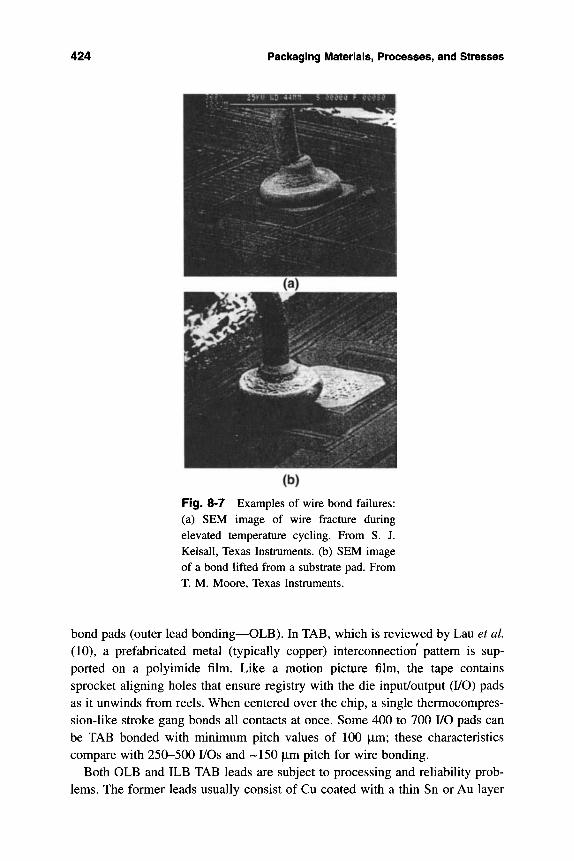
424 Packaging Materials, Processes, and Stresses
Fig. 8-7 Examples of wire bond failures: (a) SEM image of wire fracture during elevated temperature cycling. From S. J. Kelsall, Texas Instruments, (b) SEM image of a bond lifted from a substrate pad. From T. M. Moore, Texas Instruments.
bond pads (outer lead bonding—OLB). In TAB, which is reviewed by Lau et al (10), a prefabricated metal (typically copper) interconnection pattern is sup-ported on a polyimide film. Like a motion picture film, the tape contains sprocket aligning holes that ensure registry with the die input/output (I/O) pads as it unwinds from reels. When centered over the chip, a single thermocompres-sion-like stroke gang bonds all contacts at once. Some 400 to 700 I/O pads can be TAB bonded with minimum pitch values of 100 |im; these characteristics compare with 250-500 I/Os and '-150 jLim pitch for wire bonding.
Both OLB and ILB TAB leads are subject to processing and reliability prob-lems. The former leads usually consist of Cu coated with a thin Sn or Au layer
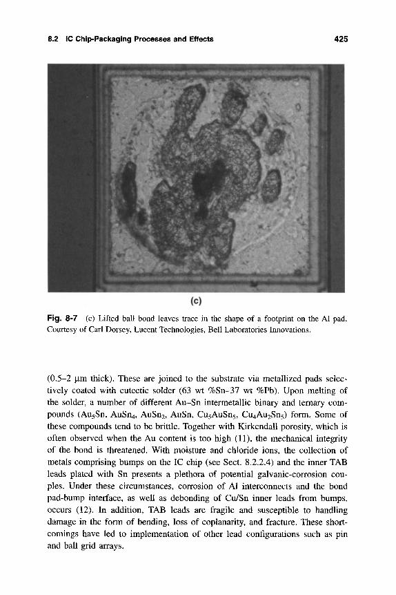
8.2 IC Chip-Packaging Processes and Effects 425
Fig. 8-7 (c) Lifted ball bond leaves trace in the shape of a footprint on the Al pad. Courtesy of Cari Dorsey, Lucent Technologies, Bell Laboratories Innovations.
(0.5-2 |im thick). These are joined to the substrate via metalHzed pads selec-tively coated with eutectic solder (63 wt %Sn-37 wt %Pb). Upon melting of the solder, a number of different Au-Sn intermetalUc binary and ternary com-pounds (AusSn, AuSn4, AuSn2, AuSn, CusAuSus, Cu4Au2Sn5) form. Some of these compounds tend to be brittle. Together with Kirkendall porosity, which is often observed when the Au content is too high (11), the mechanical integrity of the bond is threatened. With moisture and chloride ions, the collection of metals comprising bumps on the IC chip (see Sect. 8.2.2.4) and the inner TAB leads plated with Sn presents a plethora of potential galvanic-corrosion cou-ples. Under these circumstances, corrosion of Al interconnects and the bond pad-bump interface, as well as debonding of Cu/Sn inner leads from bumps, occurs (12). In addition, TAB leads are fragile and susceptible to handling damage in the form of bending, loss of coplanarity, and fracture. These short-comings have led to implementation of other lead configurations such as pin and ball grid arrays.
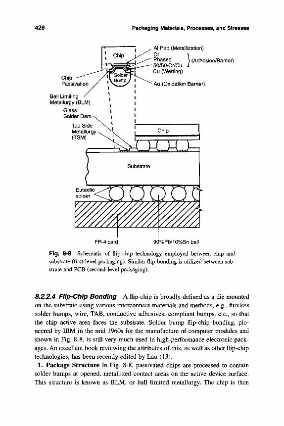
426 Packaging Materials, Processes, and Stresses
Chip Passivation
Bali Limiting l\/letallurgy (BLIVI)
Glass Solder Dam
Top Side Metallurgy (TSM)
Al Pad (Metallization) Cr 1 Phased \ (Adhesion/Barrier) 50/50/Cr/Cu J Cu (Wetting)
Au (Oxidation Barrier)
FR-4 card 90%Pb/10%Snball
Fig. 8-8 Schematic of flip-chip technology employed between chip and substrate (first-level packaging). Similar flip-bonding is utilized between sub-strate and PCB (second-level packaging).
8.2.2.4 Flip-Chip Bonding A flip-chip is broadly defined as a die mounted on the substrate using various interconnect materials and methods, e.g., fluxless solder bumps, wire, TAB, conductive adhesives, compliant bumps, etc., so that the chip active area faces the substrate. Solder bump flip-chip bonding, pio-neered by IBM in the mid 1960s for the manufacture of computer modules and shown in Fig. 8-8, is still very much used in high-performance electronic pack-ages. An excellent book reviewing the attributes of this, as well as other flip-chip technologies, has been recently edited by Lau (13).
1. Package Structure In Fig. 8-8, passivated chips are processed to contain solder bumps at opened, metallized contact areas on the active device surface. This structure is known as BLM, or ball limited metallurgy. The chip is then
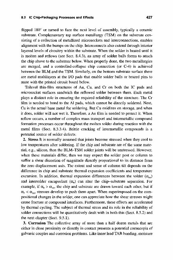
8.2 IC Chip-Packaging Processes and Effects 427
flipped 180° or turned to face the next level of assembly, typically a ceramic substrate. Complementary top surface metallurgy (TSM) on the substrate con-sisting of a collection of metallized microsockets and interconnections, enables alignment with the bumps on the chip. Interconnects also extend through interior layered levels of circuitry within the substrate. When the solder is heated until it is molten and reflows (see Sect. 8.4.3), an array of solder balls forms to attach the chip above to the substrate below. When properly done, the two metallurgies are merged, and a controlled-collapse chip connection (or C-4) is achieved between the BLM and the TSM. Similarly, on the bottom substrate surface there are metal multilayers at the I/O pads that enable solder balls or brazed pins to mate with the printed circuit board below.
Trilevel thin-film structures of Au, Cu, and Cr on both the IC pads and microsocket surfaces sandwich the reflowed solder between them. Each metal plays a distinct role in ensuring the required reliability of the structure. The Cr film is needed to bond to the Al pads, which cannot be directly soldered. Next, Cu is the actual base metal for soldering. But Cu oxidizes on storage, and when it does, solder will not wet it. Therefore, a Au film is needed to protect it. When reflow occurs, a number of complex mass transport and intermetallic compound formation processes occur throughout the molten solder during reaction with the metal films (Sect. 8.3.3.4). Brittle cracking of intermetallic compounds is a potential source of solder defects.
2. Stress It is normally assumed that joints become stressed when they cool to low temperatures after soldering. If the chip and substrate are of the same mate-rial, e.g., silicon, then the BLM-TSM solder joints will be unstressed. However, when these materials differ, then we may expect the solder post or column to suffer a shear distortion of magnitude directly proportional to its distance from the zero displacement axis. The extent and sense of column tilt depends on the difference in chip and substrate thermal expansion coefficients and temperature excursion. In addition, thermal expansion differences between the solder (ago) and intersolder encapsulant (ttg) can alter the chip-substrate separation. For example, if a^ > a^^, the chip and substrate are drawn toward each other, but if oCe < oCso, stresses develop to push them apart. When superimposed on the com-positional changes in the solder, one can appreciate how the shear stresses might cause fracture at compound interfaces. Furthermore, these effects are accelerated by thermal cycling. The subject of thermal stress and its role in the reliability of solder connections will be quantitatively dealt with in both this (Sect. 8.5.2) and the next chapter (Sect. 9.5.1).
3. Corrosion The collective array of more than a half dozen metals that are either in close proximity or directly in contact presents a potential cornucopia of galvanic couples and corrosion problems. Like inner lead TAB bonding, moisture
428 Packaging Materials, Processes, and Stresses
and impurity (CI", Na'^)-induced corrosion of positive and negatively biased Al tracks, reaction at solder bump interfaces, passivation cracking due to corrosion products, and debonding are degradation processes that can affect flip-chip bonded structures (11). Similar studies by Frankel et al. (14) found that corro-sion susceptibility of Cr/Cu, with attendant crack initiation and loss of adhesion at the pad edge, was reduced by interposing a thin Ni film between these metals.
Flip-chip bonding is also used in attaching many chips to a single substrate. The advantages of doing this, including packaging of the entire multichip mod-ule, are discussed in Sect. 8.2.3.4. Now, however, we turn to the problem of enclosing individual IC chips.
8.2.3 Chip Encapsulation
The flip-chip structure, with its passivation everywhere except at the solder, nat-urally protects the silicon device surface and needs no further enclosure. But the wire bonded chips must be sealed within containers or packages in such a way that the chip and first-level contact pads are protected. Furthermore, leads must pass through the package and be available for second-level interconnection.
8.2.3.1 Processing Plastic Pacloges Enclosing chips within polymer molding compounds is the most popular way to package integrated circuits (7, 15). In fact, more than 90% of all packages produced are of the plastic variety; they enjoy a virtual monopoly in the civilian sector and have been increasingly accepted in military applications. Annually, close to 100 billion plastic dual-in-line packages (DIPs) are produced worldwide. Epoxies containing curing agents, fillers, flame retardants, mold release compounds, and coloring agents are typi-cally employed and are molded into packages via a sequence of steps that includes 1. placement of leadframes in molds, 2. conditioning, preheating, and loading of molding compound, 3. transfer or injection molding, and 4. curing and ejection. Extreme care must be taken to minimize molding defects and yield losses in this relatively low-tech (and cheap) packaging step to preserve the fruits of high-tech (and expensive) chip-level processing.
Many defects found in plastic packages originate from the thermal stresses of processing. For example, the thermal expansion coefficients of four key compo-nents within packages, i.e., chip (4.4 x 10~^ °C~^), alloy lead frame (-4.0 - 4.7 X 10"^ °C"^), copper (17 x 10"^ °C"^) and molding compound (--20 x 10"^ °C"^) differ. This implies that stresses will develop between different pairs of contact-ing materials and foster interfacial delamination and even component cracking. Delaminated regions between the molding polymer and metal leads can be the
8.2 IC Chip-Packaging Processes and Effects 429
(CI-)—:a=.
PROTECT LAYER
MOUNTING EPOXY
Fig. 8-9 Chloride corrosion path along lead frame, bond wire and chip pad in a plastic IC package. From L. Gallance and M. Rosenfeld, RCA Review 45, 256 (1984).
conduits for moisture and chloride ion ingress to foster corrosion, as Fig. 8-9 suggests. Aided and abetted by ionic species (e.g., Br~ ) and oxygen contained within epoxy encapsulant-flame retardants, corrosion can lead to AI2O3 forma-tion and wire-bond lift-off (16).
Stresses in lead frames (17) and wire bonds (18) arising from the fluid flow of the polymer during the transfer molding process are additional sources of defects. Calculations by Suhir and Manzione have shown that the maximum stress in the wire is proportional to the square of the ratio of the wire-bond span to the wire diameter. Stresses could be large enough to lift or sweep the wire from the bonding pad. In the case of leadframes, flow-induced forces can cause lead deflections. The forces arise because the leadframe edge splits the flow of the molding compound into two mismatched flow fronts, one above and one below the sheet-metal plane. This asynmietric flow exerts a net pressure that deforms the cantilever leads. Analysis has predicted that lead deflection varies directly as the fifth power of the lead length and inversely as the third power of the lead thickness.
8.2.3.2 Popcorn Cracking After the apparently successful development of plastic encapsulation, it was observed that the frequency of so-called "popcorn" cracking of packages increased during the summer months. Furthermore, these failures occurred considerably after molding and usually during solder reflow of surface-mounted packages. These two observations strongly suggested that
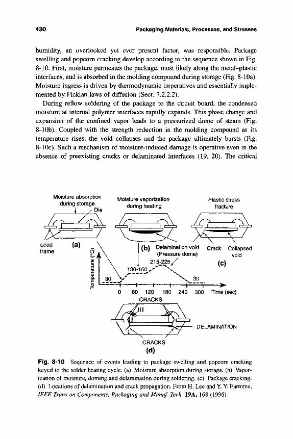
430 Packaging Materials, Processes, and Stresses
humidity, an overlooked yet ever present factor, was responsible. Package swelling and popcorn cracking develop according to the sequence shown in Fig. 8-10. First, moisture permeates the package, most likely along the metal-plastic interfaces, and is absorbed in the molding compound during storage (Fig. 8-10a). Moisture ingress is driven by thermodynamic imperatives and essentially imple-mented by Fickian laws of diffusion (Sect. 7.2.2.2).
During reflow soldering of the package to the circuit board, the condensed moisture at internal polymer interfaces rapidly expands. This phase change and expansion of the confined vapor leads to a pressurized dome of steam (Fig. 8-lOb). Coupled with the strength reduction in the molding compound as its temperature rises, the void collapses and the package ultimately bursts (Fig. 8-lOc). Such a mechanism of moisture-induced damage is operative even in the absence of preexisting cracks or delaminated interfaces (19, 20). The critical
Moisture absorption during storage
Moisture vaporization during treating
Plastic stress fracture
^ ^ ^ - T ^ \
Lead (a) _ frame o
> ^ ^
|L--f
(b ) Delamination void Crack Collapsed (Pressure dome) void
215^225 / (c )
^^^^ 30 1 h=^=^^ t >--t-
0 60 120 180 240 300 Time (sec) CRACKS
DELAMINATION
Fig. 8-10 Sequence of events leading to package swelling and popcorn cracking keyed to the solder heating cycle, (a) Moisture absorption during storage, (b) Vapor-ization of moisture, doming and delamination during soldering, (c) Package cracking, (d) Locations of delamination and crack propagation. From H. Lee and Y. Y. Earmme, IEEE Trans on Components, Packaging and Manuf. Tech. 19A, 168 (1996).
8.2 IC Chip-Packaging Processes and Effects 431
condition for package cracking is simply Gp > Gs, where Gp is the maximum stress at the edge of the die pad, and Gs is the strength of the molding compound at the soldering temperature. Furthermore, larger die pad (LDP) and thinner encapsulant thickness (Lp) dimensions both increase Gp and promote the ten-dency to cracking; larger pads allow for more potential damage sites, while thin-ner encapsulants enable moisture to penetrate more readily. A suggested formula for the onset of cracking is thus
a^ = K^-f^Pn^o, (8-2)
where (PH2O) is the water vapor pressure and K is a constant of proportionality. Three types of popcorn cracks are observed, as shown in Fig. 8-lOd. Types 1
and 11 nucleate as a result of delamination at the paddle-encapsulant interface. Cracks initiate below and above the paddle and propagate downward or upward, respectively, to the package surface. Type HI cracks nucleate at the die comer and propagate upward. Once cracking of the plastic occurs, weakened or lifted wirebonds and die-surface delamination threaten package integrity. Further ingress of moisture and contaminants is then facilitated, raising prospects for corrosion.
The primary way to prevent package popcoming is baking prior to solder reflow in order to remove moisture. Other methods include desiccant bagging of all moisture-sensitive devices, mechanically strengthening and toughening mold-ing compounds to resist fracture, and enhancing the ability of these materials to prevent water diffusion and absorption. Groothuis et al. (21) have recently dis-cussed the mechanical behavior of molding polymers and suggested metrics for selecting them.
8.2.3.3 Hermetic Packages Due to their perceived reUability advantages over plastic packages, hermetically sealed packages have found favor in military and high-risk applications. Hermetic packages encase the integrated-circuit chips within boxes and enclosures made of ceramics and metal alloys and allow for interconnection to the next packaging level, e.g., a PCB. Alumina is the most widely used ceramic in packages known as CERDIPs and CERPACs. Its low thermal conductivity makes AI2O3 unsuited for power packages, and therefore AIN and BeO have also been employed. Either flip-chip or chips on lead frames are essentially installed within the open ceramic boxes, interconnected to the package pins, and then sealed with a ceramic lid. Glass frits that must be heated, as well as epoxies and solders, are used as sealant materials in both lids and pins. One has only to recall the disaster caused by the spaceship Challenger's gaskets to realize that sealants and the technology of sealing are conmion causes of
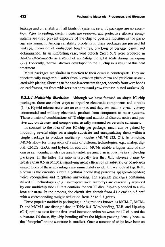
432 Packaging Materials, Processes, and Stresses
leakage and unreliability in all kinds of systems; ceramic packages are no excep-tion. Prior to sealing, contaminants are removed and protective silicone encap-sulants are used prevent exposure of the chip to possible moisture in the pack-age environment. Among reliability problems in these packages are pin and lid leakage, corrosion of embedded bond wires, cracking of ceramic cases, and delamination. In an interesting case, void defects (Sect. 5.7) were produced in Al-Cu interconnects as a result of annealing the glass seals during packaging (22). Evidently, thermal stresses developed in the IC chip as a result of this heat treatment.
Metal packages are similar in function to their ceramic counterparts. They are mechanically tougher but suffer from corrosion phenomena and problems associ-ated with plating. Shorting to the case is a constant danger, not only from wire bonds or lead frames, but from whiskers that sprout and grow from tin-plated surfaces (6).
8.2.3.4 Multlchip Modules Although we have focused on single IC chip packages, there are other ways to organize electronic components and circuits (1-4). Hybrid microcircuits are an example, and they are used in virtually every commercial and military electronic product from computers to radar systems. These consist of combinations of IC chips and additional discrete active and pas-sive add-on devices and components, usually mounted on ceramic substrates.
In contrast to the idea of one IC chip per package, much can be gained by mounting several chips on a single substrate and encapsulating them within a single package to produce multichip modules (MCM) (23, 24). In principle, MCMs allow for integration of a mix of different technologies, e.g., analog, dig-ital, CMOS, GaAs, and hybrid. In addition, MCMs enable a higher ratio of sih-con or semiconductor-device area to substrate area than is possible in single-chip packages. In the latter this ratio is typically less than 0.1, whereas it may be greater than 0.5 in MCMs, signifying great efficiency in substrate or board-area usage. Both of these advantages are immediately evident if we look at Fig. 8-11. Shown is the circuitry within a cellular phone that performs speaker-dependent voice recognition and telephone answering. Ten separate packages containing mixed IC technologies (e.g., microprocessor, memory) are essentially replaced by one multichip module that contains the ten IC dies, flip-chip bonded to a sil-icon substrate. In the process, the circuit size shrank from 43.2 cm^ to 6.5 cm^ with a corresponding weight reduction from 32 to 2.3 grams.
Three popular multichip packaging configurations known as MCM-C, MCM-D, and MCM-L are distinguished in Table 8-4. Wire bonding, TAB, and flip-chip (C-4) options exist for the first-level interconnection between the IC chip and the substrate. Of these, flip-chip bonding offers the highest packing density because the "footprint" on the substrate is smallest. Once a number of chips have been so
8.2 IC Chip-Packaging Processes and Effects 433
Fig. 8-11 Voice recognition/telephone answering device. Above: Circuit board assembly module. Below: Multichip module on a test board. From B. J. Han, S. Das, R. C. Frye, K. L. Tai, and M. Y. Lau, IEEE Multi-Chip Module Con-ference, Santa Cruz, California, p. 45, Jan. 31, 1995. Cour-tesy of K. L. Tai and R. C. Frye, Lucent Technologies, Bell Laboratories Innovations.
bonded to a substrate, the entire assembly may, for example, be molded within a single plastic package.
Improvement in system performance and reliability are the chief advantages of a multichip module, now acting as a unit, relative to the traditional one-chip packages. The latter may have some ten times the number of connections and six times the wiring length relative to the MCM package (24).
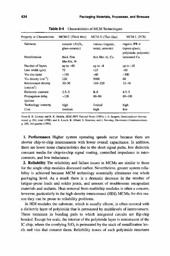
434 Packaging Materials, Processes, and Stresses
Table 8-4 Characteristics of MCM Technologies
Property or Characteristic
Substrate
Metallization
Number of layers Line width (jxm) Via size ( im) Via density (cm~ ) Interconnect density (cm/cm^) Dielectric constant Propagation delay (ps/cm) Technology maturity Cost
MCM-C (Thick film)
ceramic (AI2O3, glass-ceramic)
thick film Mo-Mn,W up to --60 75 -150 120 20-30
2.5-3 -120
high medium
MCM-D (Thin film)
various (organic, metal, ceramic)
thin film Al, Cu
up to ~8 <25 -60 5000 160-320
8-9 60-80
limited high
MCM-L (PCB)
organic (FR-4 (epoxy-glass), polyimide, polyester) laminated Cu
up to -50 -65 -300 60 12-16
4.5-5 80-100
high low
From B. R. Livesay and R. K. Shukla, IEEE IRPS Tutorial Notes (1993); J. E. Sergent, Semiconductor Interna-tional, p. 263, June (1996), and K. Losch, K. Allaert, S. Smemos, and J. Novotny, Electronics Communications, p. 260, 3rd quarter (1993).
1. Performance Higher system operating speeds occur because there are shorter chip-to-chip interconnects with lower overall capacitance. In addition, there are lower noise characteristics due to the short signal paths, low dielectric constant media for chip-to-chip signal routing, controlled impedance in inter-connects, and low inductance.
2. Reliability The reliability and failure issues in MCMs are similar to those for the single-chip modules discussed earlier. Nevertheless, greater system relia-bility is achieved because MCM technology essentially eliminates one whole packaging level. As a result there is a dramatic decrease in the number of fatigue-prone leads and solder joints, and amount of troublesome encapsulant materials and sealants. Heat removal from multichip modules is often a concern, however, particularly in the high-density interconnect (HDI) MCMs; for this rea-son they can be prone to reliability problems.
In HDI modules the substrate, which is usually silicon, is often covered with a dielectric layer of polyimide that is permeated by multilevels of interconnects. These terminate in bonding pads to which integrated circuits are flip-chip bonded. Except for scale, the interior of the polyimide layer is reminiscent of the IC chip, where the overlying Si02 is permeated by the stack of metallization lev-els and vias that connect them. Reliability issues of such polyimide structures
8.3 Solders and Their Reactions 435
involve metal-polyimide interactions, difficulty in wire bonding to Al pads, polyimide decomposition, and cracking. While the polyimide-Al interface is inert, Cu interconnects are chemically unstable, and if used require diffusion bar-riers. In addition, polyimide can carbonize during processing, causing loss of metal adhesion and surface leakage currents. Simultaneous volume shrinkage during curing can cause polyimide cracking as well.
8.3 SOLDERS AND THEIR REACTIONS
8.3.1 Introduction
For making permanent interconnections, solders have the great virtue of enabling low-temperature joining of metallic conductors to establish low-resistance ohmic electrical performance at all packaging levels. Solders also provide mechanical support of components and are, in some cases, a conduit for heat transfer. How-ever, together with their excellent electrical and joining characteristics, they have attributes that make them a source of processing defects, and they are susceptible to a number of reliability problems. The former issues will be addressed in this chapter, while the latter concerns will be primarily reserved for Chapter 9. In addi-tion to inclusion in the references dealing with packaging, there are a number of books (25-27) devoted solely to solder materials, processes, and reliability issues that are worth consulting.
Let us start by reviewing some elementary aspects of solder metallurgy. The phase diagram for Pb-Sn, a system that exhibits eutectic solidification, is shown in Fig. 8-12. In addition to Pb--Sn, three other eutectic systems play a role in this book. Within the Au-Si system, a solder-like eutectic alloy is used to bond or attach integrated circuits to the metal frame during the packaging of IC chips. Those with good memories will also recall that similar eutectic systems consist-ing of Al-Cu and Al-Si have relevance to electromigration and contact reliabil-ity, respectively (see Chapter 5).
Upon solidification of the eutectic solder alloy (61.9 wt %Sn-38.1 wt %Pb), a eutectic transformation occurs at the critical isotherm 183°C according to the reaction
Eutectic L(61.9 wt %Sn) ^-^^ a (19 wt %Sn) +p (97.5 wt %Sn) (8-3)
Since the alloy undergoes eutectic solidification, the proeutectic phase is embed-ded within the two-phase eutecticmicrostructure. Equilibrium at 183°C implies that phase compositions given by the tie lines are a (19 wt %Sn) and (3 (97.5 wt
436 Packaging Materials, Processes, and Stresses
400
40 60 Weight percent tin
Fig. 8-12 Equilibrium phase diagram for Pb-Sn
80 Sn
%Sn). Just below 183°C the Lever Rule predicts a eutectic mixture composed of 45.4 wt % a and 54.6 wt % p.
While this standard equilibrium analysis provides information on phase com-positions and amounts, it says nothing about phase morphologies; these are dependent instead on prior processing history. For example, the cooling rate dur-ing electronic soldering operations is often too fast for thermodynamic equilib-rium conditions to prevail. Rapid cooling of solders yields fine microstructures, i.e., those with a large number of small features. Finer-grained cast structures, characterized by small interdendritic spacings, are generally stronger, but they are also metastable. Provided that sufficient thermal energy is available for the neces-sary atom movements, there will be a gradual solid-state transformation towards equilibrium structures and solubilities dictated by the phase diagram. Because of their low melting points, room temperature for solders is actually about 0.65 of T^ (JM is the absolute melting point in K). At such high homologous temperatures, atoms diffuse and metals creep at observable rates. And during higher-tempera-
8.3 Solders and Their Reactions 437
Fig. 8-13 Coarsening of Pb-Sn solidified solder structure as a function of room temperature aging, (a) 2 hours, (b) 17 days, (c) 34 days, (d) 63 days. Lead and tin appear white and black, respectively. From R. D. Denman, Tin and Its Uses, No. 165, 16 (1991).
ture operation, even more thermal energy is available to accelerate transforma-tions. Thus the structure that forms during solidification is gradually altered, as shown in Fig. 8-13. Simultaneously, the solder loses strength over a period of a few days or weeks, a phenomenon known as age softening. The cause of the soft-ening is the relieval of supersaturation within the eutectic matrix. Continued coarsening due to diffusion of atoms continues for years but has a much lesser effect on room-temperature mechanical properties since the solder strength stabi-lizes after a few weeks. It takes little imagination to grasp the potential reliability implications of time-dependent structural change in solder contacts.
Chemical and structural change can also occur during thermal cycling, a com-mon service environment. Solders will then undergo cycles of phase precipita-tion and dissolution in concert. If the thermal cycle frequency is low, both the precipitation and dissolution processes may go to completion at low and high temperatures, respectively. However, if the thermal cycle frequency is high, nei-ther precipitation or dissolution will approach completion during a cycle; some
438 Packaging Materials, Processes, and Stresses
steady-state structure, different from that at equilibrium, may then evolve. The influence of chemical and morphological change must always be home in mind when assessing solder reliability, even at room temperature.
8.3.2 Solder Properties
The composition of a broad number of electrical solder alloys and their relevant properties are tabulated in Table 8-5. Binary eutectic, and near-eutectic tin-lead alloys have traditionally dominated soft-solder usage in both electrical and plumbing appHcations. It is not surprising, therefore, that both of these elements have served as the basis for developing improved multicomponent alloys con-taining varying additions of indium, bismuth, silver, antimony, etc. Lead, how-ever, is toxic, and in recent years environmental regulations have mandated reduced levels of Pb exposure and total elimination of this metal in various prod-ucts. Although legislation has not yet curtailed the use of Pb in electronic sol-ders, such action will probably occur in the not-too-distant future, with poten-tially significant implications for joining and packaging reliability (28).
Solders tend to be more electrically resistive than the base metals they inter-connect. However, because the length-to-area ratio of solder joints is low, negli-gible resistance is added to the electrical circuit. Resistivity, of course, depends on temperature, and the data in Table 8-5 are for 20°C. Interestingly, many sol-der alloys are superconducting at temperatures near 4K. Thermal-expansion coefficients for solder alloys are usually higher than those of the metals they interconnect. Thus a solder droplet that solidifies and wets a metal surface is expected to be stressed in residual tension while the underlying metal is com-pressed.
Solders are mechanically weak materials with strengths typically an order of magnitude less than those for structural aluminum and copper alloys (29). Importantly, solder alloys are susceptible to low-temperature creep deformation. Young's modulus for these materials ranges between 21 GPa and 55 GPa (3 to 8 X 10^ psi) (30). Tin is harder, stronger, and stiffer than lead; e.g.. Young's mod-uli for Sn and Pb are 50 GPa and 14 GPa, respectively. If one thinks of Pb-Sn solders as composites whose overall properties are weighted averages of those of the two constituent phases, it is easy to see why both the tensile strength and Young's modulus increase directly with Sn content.
8.3.3 Metal-Solder Reactions
8.3.3.1 Wetting In considering the interaction of solder with a base metal surface, the question of wetting is the primary issue. Solder has a reasonably high surface tension (YS), SO that it, like mercury, tends to ball up when molten.
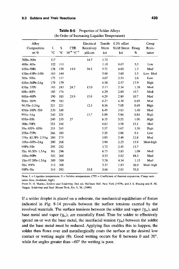
8.3 Solders and Their Reactions 439
Table 8-5 Properties of Solder Alloys (In Order of Increasing Liquidus Temperature)
Alloy Composition
wt %
50Sn-50In 40Sn-60In 42Sn-58Bi 43Sn-43Pb-14Bi 30In-70Sn 62Sn-36Pb-2Ag 63Sn-37Pb 60In^0Pb 60Sn-40Pb 80Sn-20Pb 96.5Sn-3.5Ag 85Sn-10Pb-5Sb 95Sn-5Ag 95Sn-5Sb 30In-70Pb 5Sn-85Pb-10Sb 25Sn-75Pb 15Sn-82.5Pb-2.5Ag 10Sn-88Pb-2Ag 95Pb-5Sb 5Sn-93.5Pb-l.5Ag 10Sn-90Pb lSn-97.5Pb-l.5Ag 5Sn-95Pb 95Pb-51n
L °C
117 122 138 163 175 179 183 185 190 199 221 230 240 240 253 255 266 280 290 295 301 302 309 312 314
S °C
113 138 144 117 179 183 174 183 183 221 188 221 235 240 245 183 275 268 252 296 268 309 308 292
CTE jQ-6 o(.-l
14.9
24.7
23.9
27
Electrical Resistivity
|iQ-cm
14.7
34.5
15.0
15.0
12.3
13.7
33.8
Tensile Stress
ksi
1.72 1.10 9.71 5.60 4.67 4.50 5.13 4.29 4.29 6.27 8.36 6.45 8.09 8.15 4.83 5.57 3.35 3.85 3.94 3.72 6.75 3.53 5.58 3.37 3.66
0.2% offset Yield Stress
ksi
0.67 6.03 3.60 2.54 2.57 2.34 2.89 2.89 4.30 7.08 3.63 5.86 5.53 3.58 3.67 2.06 2.40 2.25 2.45 3.85 2.02 4.34 1.93 2.01
Elong
%
5.5 1.3 2.5 2.6
17.9 1.38
10.7 10.7 0.82 0.69 1.40 0.84 1.06
15.1 3.50 8.4
12.8 15.9 13.7 1.09
18.3 1.15
26.0 33.0
Creep Resis-tance
Low Mod
Low-Mod Low High Mod Mod Mod Mod High Mod High High Mod High Low Mod
Mod-high
Mod Mod Mod
Mod-high
Note: L = Liquidus temperature, S = Solidus temperature, CTE = Coefficient of thermal expansion. Creep resis-tance (low, moderate, high). From H. H. Manko, Solders and Soldering, 2nd. ed, McGraw Hill, New York (1979), and J. S. Hwang and R. M. Vargas, Soldering and Surf. Mount Tech, No. 5, 38, (1990).
If a solder droplet is placed on a substrate, the mechanical equilibrium of forces indicated in Fig. 8-14 prevails between the surface tensions exerted by the involved materials. The surface tensions between the solder and vapor (YSV), and base metal and vapor (Ybv)» are essentially fixed. Thus for solder to effectively spread on or wet the base metal, the interfacial tension (Ysb) between the solder and the base metal must be reduced. Applying flux enables this to happen; the solder then flows over and metallurgically coats the surface at the desired low contact or wetting angle (9). Good wetting occurs for 0 between 0 and 20°, while for angles greater than '-60° the wetting is poor.
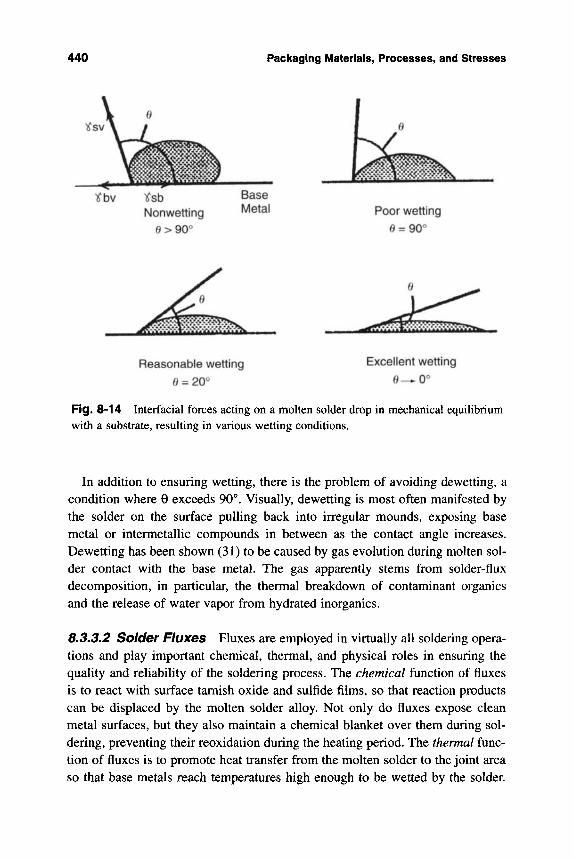
440 Packaging Materials, Processes, and Stresses
tbw Nonwetting
0>9O°
Base Metal Poor wetting
0 = 90°
Reasonable wetting
e = 20°
Excellent wetting
0 -^0°
Fig. 8-14 Interfacial forces acting on a molten solder drop in mechanical equilibrium with a substrate, resulting in various wetting conditions.
In addition to ensuring wetting, there is the problem of avoiding dewetting, a condition where 0 exceeds 90°. Visually, dewetting is most often manifested by the solder on the surface pulling back into irregular mounds, exposing base metal or intermetallic compounds in between as the contact angle increases. Dewetting has been shown (31) to be caused by gas evolution during molten sol-der contact with the base metal. The gas apparently stems from solder-flux decomposition, in particular, the thermal breakdown of contaminant organics and the release of water vapor from hydrated inorganics.
8.3.3.2 Solder Fluxes Fluxes are employed in virtually all soldering opera-tions and play important chemical, thermal, and physical roles in ensuring the quality and reliability of the soldering process. The chemical function of fluxes is to react with surface tarnish oxide and sulfide films, so that reaction products can be displaced by the molten solder alloy. Not only do fluxes expose clean metal surfaces, but they also maintain a chemical blanket over them during sol-dering, preventing their reoxidation during the heating period. The thermal func-tion of fluxes is to promote heat transfer from the molten solder to the joint area so that base metals reach temperatures high enough to be wetted by the solder.
8.3 Solders and Their Reactions 441
Finally, fluxes facilitate the physical need to reduce the interfacial surface ten-sion between the solder and the base metal.
Traditional rosin fluxes contain only three types of ingredients, namely rosin, an ammonium hydrohalide salt that serves as the activator, and lastly a solvent, often isopropanol. During soldering, the activator decomposes to release hydro-gen chloride (or bromide), which reacts with the oxide present to form small quan-tities of metallic chlorides. Most of the chloride ions are dissipated in gaseous form, but some may remain undecomposed, especially on cooler surfaces that are not in direct contact with the solder. Minute residues of chlorides, hydrohalides, and metallic rosin salts cause potential reliability problems due to ionic leakage currents. For example, NaCl contamination levels of 1 mg/cm^ have been shown to be sufficient to initiate corrosion on printed wiring boards (32).
On an electronics assembly, especially under humid conditions, ionic conduc-tion can have several deleterious effects. The four most serious are (33) as follows:
1. malfunction of the circuit due to current flow between adjacent nonequipo-tential tracks,
2. electrolytic corrosion due to the formation of reactive substances at the elec-trodes and their subsequent chemical reaction with the conductor metal (e.g., see Fig. 7-4b),
3. metal-dendrite formation due to the passage of current through an electrolyte containing metal salts, and
4. electrical noise. An ionic current is never sensibly constant, as is a purely electronic current; due to their low mobility, ions often "clump" in the elec-trolyte.
Thus, it is important either to remove as much of the ionic contamination as possible by efficient and controlled cleaning, or to render it as harmless as pos-sible.
8.3.3.3 Dissolution and Compound Formation Reactions There are important compositional changes associated with molten solder wetting of base-metal surfaces. In the case of copper, for example, a small amount first dissolves upon contact with solder. Then reaction between Cu and Sn atoms produces an intermetallic-compound layer of Cu6Sn5 at the interface. Although CugSns is hard and brittle in nature, it essentially fosters the adhesion required for reliable soldered joints. However, the thick Cu6Sn5 layers that form at elevated tempera-tures are brittle and induce premature failure. Thus, thin layers of intermetallic compounds are beneficial, but thicker layers are detrimental.
In reflow soldering processes (Sect. 8.4.4) a limited amount of solder remains molten for almost a minute. This results in a high level of dissolved copper and
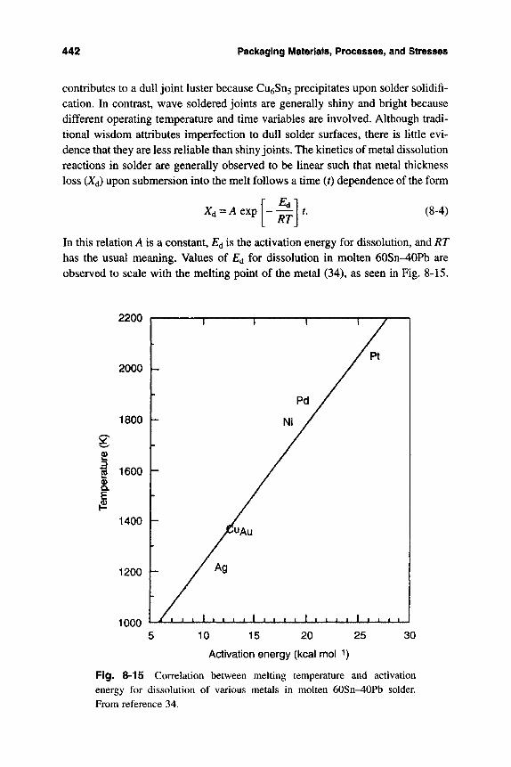
442 Packaging Materials, Processes, and Stresses
contributes to a dull joint luster because CugSus precipitates upon solder solidifi-cation. In contrast, wave soldered joints are generally shiny and bright because different operating temperature and time variables are involved. Although tradi-tional wisdom attributes imperfection to dull solder surfaces, there is little evi-dence that they are less reliable than shiny joints. The kinetics of metal dissolution reactions in solder are generally observed to be linear such that metal thickness loss (Xd) upon submersion into the melt follows a time (t) dependence of the form
RT\ X^-A exp (8-4)
In this relation A is a constant, E^ is the activation energy for dissolution, and RT has the usual meaning. Values of E^ for dissolution in molten 60Sn-40Pb are observed to scale with the melting point of the metal (34), as seen in Fig, 8-15,
2200
2000 h
1800 h
2 1600
E
1400 h
1200 h
1000
L.
[•
h
h-
u
/ 1 L
1 1—
yCUAu
/ Ag
, i 1 1 I I I 1 L
1
Pd /
Nl /
1 1 1, 1 1 1 1
—1 7—1 /p\
1 1 I I I I 1
10 15 20 25
Activation energy (kcal moJ-'')
30
Fig. 8-15 Correlation between melting temperature and activation energy for dissolution of various metals in molten 60Sn-40Pb solder. From reference 34.
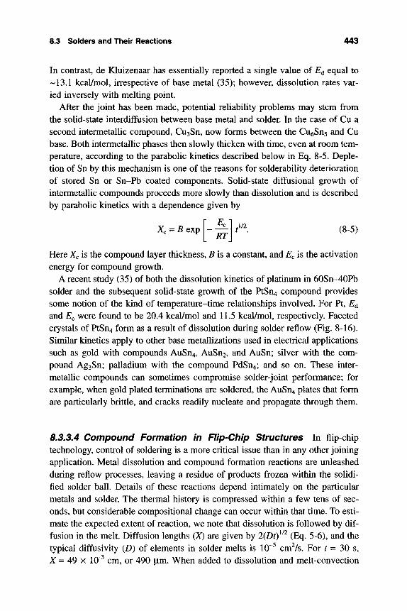
8.3 Solders and Their Reactions 443
In contrast, de Kluizenaar has essentially reported a single value of E^ equal to -13.1 kcal/mol, irrespective of base metal (35); however, dissolution rates var-ied inversely with melting point.
After the joint has been made, potential reliability problems may stem from the solid-state interdiffusion between base metal and solder. In the case of Cu a second intermetallic compound, CUBSU, now forms between the CueSus and Cu base. Both intermetallic phases then slowly thicken with time, even at room tem-perature, according to the parabolic kinetics described below in Eq. 8-5. Deple-tion of Sn by this mechanism is one of the reasons for solderability deterioration of stored Sn or Sn~Pb coated components. Solid-state diffusional growth of intermetallic compounds proceeds more slowly than dissolution and is described by parabolic kinetics with a dependence given by
Xc = B exp RT
f'\ (8-5)
Here X^ is the compound layer thickness, B is a constant, and ^c is the activation energy for compound growth.
A recent study (35) of both the dissolution kinetics of platinum in 60Sn-40Pb solder and the subsequent solid-state growth of the PtSn4 compound provides some notion of the kind of temperature-time relationships involved. For Pt, E^ and E^ were found to be 20.4 kcal/mol and 11.5 kcal/mol, respectively. Faceted crystals of PtSn4 form as a result of dissolution during solder reflow (Fig. 8-16). Similar kinetics apply to other base metallizations used in electrical applications such as gold with compounds AuSn4, AuSna, and AuSn; silver with the com-pound AgsSn; palladium with the compound PdSn4; and so on. These inter-metallic compounds can sometimes compromise solder-joint performance; for example, when gold plated terminations are soldered, the AuSn4 plates that form are particularly brittle, and cracks readily nucleate and propagate through them.
8,3,3.4 Compound Formation In Flip-Chip Structures In flip-chip technology, control of soldering is a more critical issue than in any other joining application. Metal dissolution and compound formation reactions are unleashed during reflow processes, leaving a residue of products frozen within the solidi-fied solder ball. Details of these reactions depend intimately on the particular metals and solder. The thermal history is compressed within a few tens of sec-onds, but considerable compositional change can occur within that time. To esti-mate the expected extent of reaction, we note that dissolution is followed by dif-fusion in the melt. Diffusion lengths (X) are given by 2{Dt)^'^ (Eq. 5-6), and the typical diffusivity (D) of elements in solder melts is 10"^ cm%. For r = 30 s, Z = 49 X 10" cm, or 490 \im. When added to dissolution and melt-convection
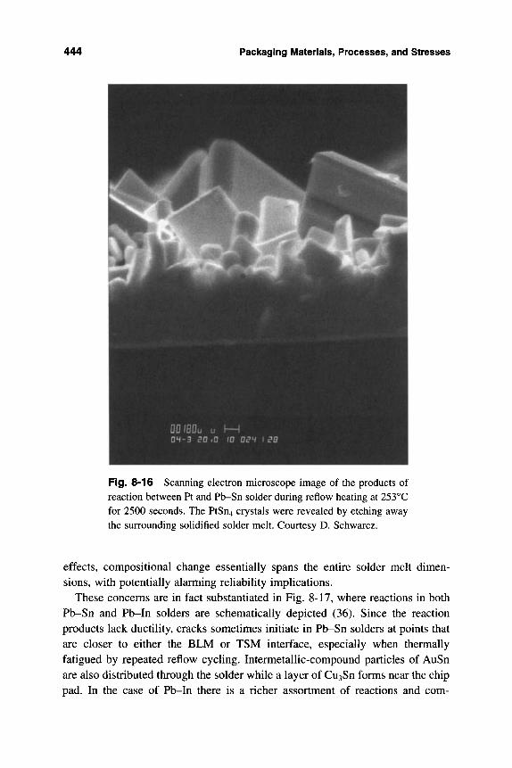
444 Packaging Materials, Processes, and Stresses
Fig. 8-16 Scanning electron microscope image of the products of reaction between Pt and Pb-Sn solder during reflow heating at 253°C for 2500 seconds. The PtSn4 crystals were revealed by etching away the surrounding solidified solder melt. Courtesy D. Schwarcz.
effects, compositional change essentially spans the entire solder melt dimen-sions, with potentially alarming reliability implications.
These concerns are in fact substantiated in Fig. 8-17, where reactions in both Pb-Sn and Pb-In solders are schematically depicted (36). Since the reaction products lack ductility, cracks sometimes initiate in Pb-Sn solders at points that are closer to either the BLM or TSM interface, especially when thermally fatigued by repeated reflow cycling. Intermetallic-compound particles of AuSn are also distributed through the solder while a layer of Cu3Sn forms near the chip pad. In the case of Pb-In there is a richer assortment of reactions and com-
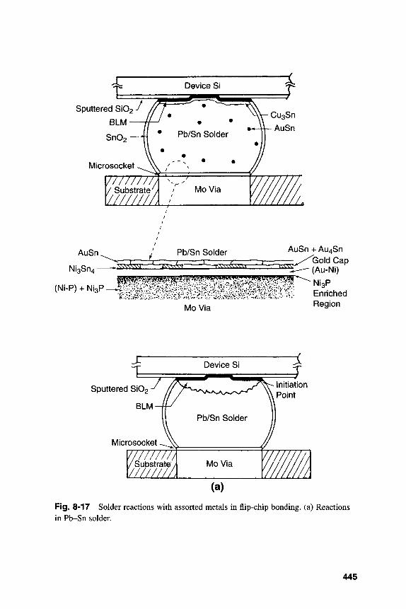
^ t Sputtered Si02
B L M -
Sn02
Microsocket
Device Si
AuSn,
Ni3Sn4 -
Pb/Sn Solder / s Tsss\^ssssv: 2CSS2^
Mo Via
AuSn + Au4Sn i=;:^^^^o\6 Cap
(Au-Ni)
NisP Enriched Region
ry Sputtered Si02
BLM
Microsocket
Device Si
Initiation Point
/ / / / / / / / / /Substrate/ Mo Via •
(a)
Fig. 8-17 Solder reactions with assorted metals in flip-chip bonding, (a) Reactions in Pb-Sn solder.
445
Sputtered Si02
BLM-Cu7ln4
Mostly Auln2 with some Auain
Auain
Gold Cap
Microsocket.
V/
CaOld Oap ^^^ M|MW*V)VJ[l J*AW ^ (Au-Ni) '•^lC^:-^vy^i^.^i^^^
(Ni-P) + NigP y^^-^i-:^i^^^i^^^h''^^^^ Mo Via
Ni27lnio
NiaP Enriched Region
•.rC7 Sputtered SIO2
BLM
Represents all layers in the TSM structure
p777777"v 1/ Substrate /
I//////// Mo Via •
Auln2 particles
Partition of Cu7ln4 between BLM and TSM Thin layer of In203
(b) Fig. 8-17 (b) Reactions in Pb-In solder. From reference 36.
446
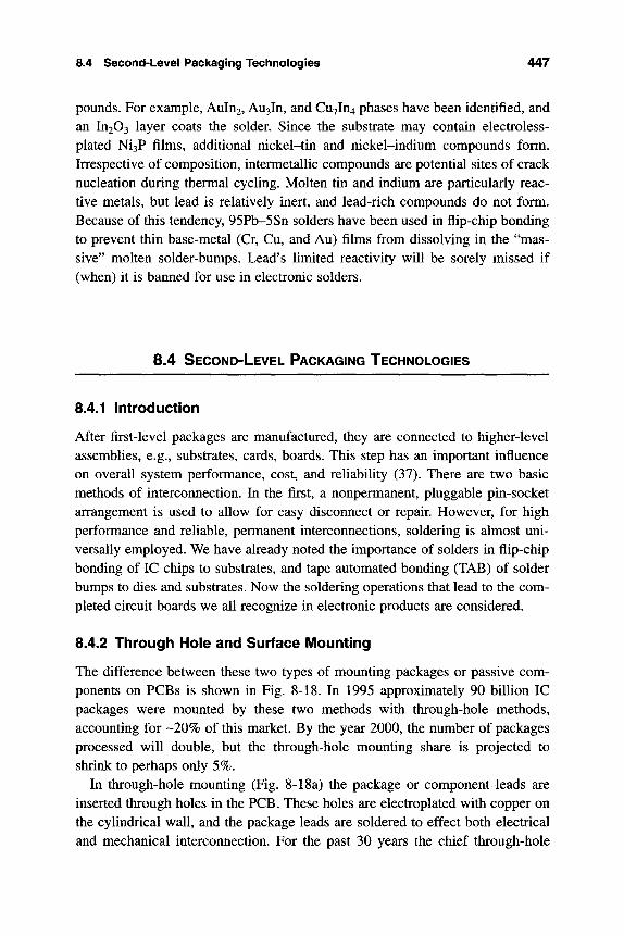
8.4 Second-Level Packaging Technologies 447
pounds. For example, Auln2, Au3ln, and Cu7ln4 phases have been identified, and an In203 layer coats the solder. Since the substrate may contain electroless-plated Ni3P films, additional nickel-tin and nickel-indium compounds form. Irrespective of composition, intermetallic compounds are potential sites of crack nucleation during thermal cycling. Molten tin and indium are particularly reac-tive metals, but lead is relatively inert, and lead-rich compounds do not form. Because of this tendency, 95Pb-5Sn solders have been used in flip-chip bonding to prevent thin base-metal (Cr, Cu, and Au) films from dissolving in the "mas-sive" molten solder-bumps. Lead's limited reactivity will be sorely missed if (when) it is banned for use in electronic solders.
8-4 SECOND-LEVEL PACKAGING TECHNOLOGIES
8.4.1 Introductioh
After first-level packages are manufactured, they are connected to higher-level assemblies, e.g., substrates, cards, boards. This step has an important influence on overall system performance, cost, and reliability (37). There are two basic methods of interconnection. In the first, a nonpermanent, pluggable pin-socket arrangement is used to allow for easy disconnect or repair. However, for high performance and reliable, permanent interconnections, soldering is almost uni-versally employed. We have already noted the importance of solders in flip-chip bonding of IG chips to substrates, and tape automated bonding (TAB) of solder bumps to dies and substrates. Now the soldering operations that lead to the com-pleted circuit boards we all recognize in electronic products are considered.
8.4.2 Through Hole and Surface Mounting
The difference between these two types of mounting packages or passive com-ponents on PCBs is shown in Fig. 8-18. In 1995 approximately 90 billion IG packages were mounted by these two methods with through-hole methods, accounting for -20% of this market. By the year 2000, the number of packages processed will double, but the through-hole mounting share is projected to shrink to perhaps only 5%.
In through-hole mounting (Fig. 8-18a) the package or component leads are inserted through holes in the PCB. These holes are electroplated with copper on the cylindrical wall, and the package leads are soldered to effect both electrical and mechanical interconnection. For the past 30 years the chief through-hole
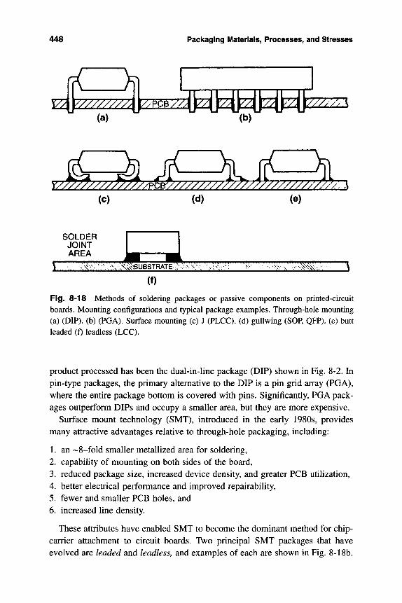
448 Packaging Materials, Processes, and Stresses
^ y///////7\ fc/.pcB /x (a)
V/////\ (b)
SOLDER JOINT AREA
:>^ . - - • - .V Ov^gUBSTRATE-.::
(f)
Fig. 8-18 Methods of soldering packages or passive components on printed-circuit boards. Mounting configurations and typical package examples. Through-hole mounting (a) (DIP), (b) (PGA). Surface mounting (c) J (PLCC). (d) gullwing (SOP, QFP). (e) butt leaded (f) leadless (LCC).
product processed has been the dual-in-line package (DIP) shown in Fig. 8-2. In pin-type packages, the primary alternative to the DIP is a pin grid array (PGA), where the entire package bottom is covered with pins. Significantly, PGA pack-ages outperform DIPs and occupy a smaller area, but they are more expensive.
Surface mount technology (SMT), introduced in the early 1980s, provides many attractive advantages relative to through-hole packaging, including:
1. an '-8-fold smaller metallized area for soldering, 2. capability of mounting on both sides of the board, 3. reduced package size, increased device density, and greater PCB utiHzation, 4. better electrical performance and improved repairability, 5. fewer and smaller PCB holes, and 6. increased line density.
These attributes have enabled SMT to become the dominant method for chip-carrier attachment to circuit boards. Two principal SMT packages that have evolved are leaded and leadless, and examples of each are shown in Fig. 8-18b.
8.4 Second-Level Packaging Technologies 449
(Note that lead is pronounced here as "leed.") Leaded packages have compUant leads that extend from the package to the PCB where they are soldered. Two popular lead configurations are the "J" and "gullwing." The former are tucked under the package in a J shape. Compliant leads flex under applied loads, reduc-ing stresses and strains in the solder joint. On the other hand, in leadless pack-ages, solder forms a more rigid bridge between the metallized areas of the pack-age and the PCB. The basic difference between leaded and leadless SMT is the elastic compliance of the lead. As we shall see in Section 9.5.2, this factor becomes significant when the response of leadless and leaded solder joints to thermal cycling is treated.
8.4.3 Ball Grid Arrays
Increasing transistor-gate counts have perpetually driven the development of smaller packages with ever more input/output connections. These I/O demands have driven peripherally leaded surface-mounted components to smaller lead-to-lead pitches. As a result of the added complexity, circuit-board assembly yields and costs have been adversely affected. To address these problems, one of the newer packaging techniques, which will increasingly replace the leaded and leadless packages discussed above, makes use of ball grid arrays (EGA). Except for the fact that EGAs are used in second-level packaging, they are basically similar to flip-chip solder connections. This can be seen in Fig. 8-8, where the solder balls that connect the substrate (containing the previously attached flip chip) to the PCE, are part of a EGA array. In general, EGA solder balls are larger than chip solder bumps, but they continue to shrink in size in the unceas-ing quest for miniaturization. In contrast to leaded connections, the overall foot-print of the EGA on the circuit board is only slightly larger than that of the IC chip itself. Easically, all of the reliability and failure experience with flip-chip (e.g., C-4) soldering is translatable to EGA technology.
Although EGA packages exhibit good electrical and thermal performance and enhanced package and assembly yields, they are, like all new technologies, not without problems. Some stem from the lack of infrastructure and acceptance. Eecause they have hidden solder connections, EGA packages cannot be easily inspected or reworked. Latent reliability defects may be problematical, and such plastic packages are also prone to popcorn cracking.
8.4.4 Reflow and Wave Soldering Processes
There are two basic soldering processes to connect chip packages and compo-nents to PCEs, and they differ depending on the methods of solder application and subsequent heating (38). In reflow soldering, the solder is first either elec-trolytically deposited, applied as a preform, or most often selectively screened
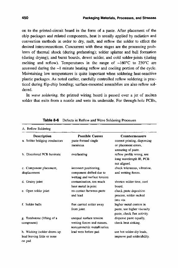
450 Packaging Materials, Processes, and Stresses
on to the printed-circuit board in the form of a paste. After placement of the chip packages and related components, heat is usually applied by radiation and convection methods in order to dry, melt, and reflow the solder to effect the desired interconnections. Concurrent with these stages are the processing prob-lems of thermal shock (during preheating); solder splatter and ball formation (during drying); and burnt boards, dewet solder, and cold solder-joints (during melting and reflow). Temperatures in the range of -160°C to 230°C are accessed during the -'I minute heating reflow and cooling portion of the cycle. Maintaining low temperatures is quite important when soldering heat-sensitive plastic packages. As noted earlier, carefully controlled reflow soldering is prac-ticed during flip-chip bonding; surface-mounted assemblies are also reflow sol-dered.
In wave soldering, the printed wiring board is passed over a jet of molten solder that exits from a nozzle and wets its underside. For through-hole PCBs,
Table 8-6 Defects in Reflow and Wave Soldering Processes
A. Reflow Soldering
Description a. Solder bridging conductors
b. Discolored PCB laminate
c. Component placement, displacement
d. Grainy joint
e. Open solder joint
f. Solder balls
g. Tombstone (lifting of a component)
h. Wicking (solder draws up lead leaving little or none on pad
Possible Causes paste formed single meniscus
overheating
incorrect positioning, component drifted due to wetting and surface tension contamination, too much base metal in joint no contact between paste and lead
flux carried solder away from joint
unequal surface tension wetting forces and masses, nonsymmetric metallization lead wets before pad
Countermeasure correct printing, dispensing or placement errors, smearing of paste, reflow profile wrong, use long wavelength IR, PCB not aligned.
check tolerances, vibration, and wetting forces.
shorten solder time, cool board. check paste deposition process, solder sucked into via. higher metal content in paste, use higher viscosity paste, check flux activity. dispense paste equally, check heat sinking.
use hot solder-dip leads, improve pad solderability.
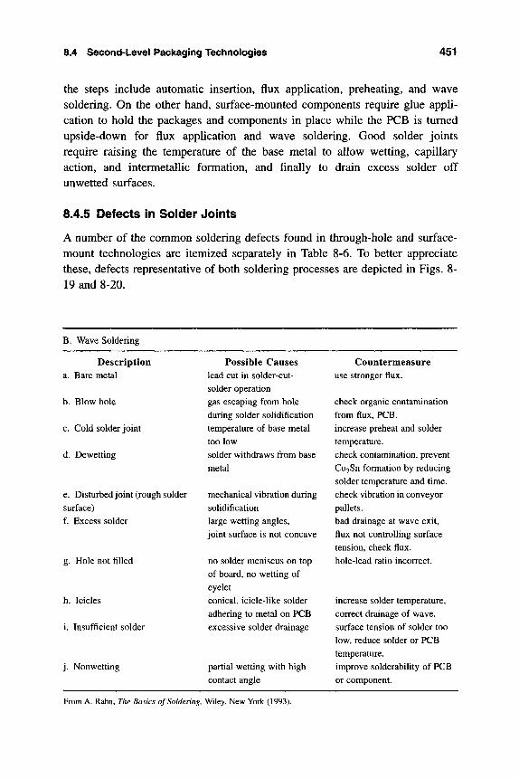
8.4 Second-Level Packaging Technologies 451
the steps include automatic insertion, flux application, preheating, and wave soldering. On the other hand, surface-mounted components require glue appli-cation to hold the packages and components in place while the PCB is turned upside-down for flux application and wave soldering. Good solder joints require raising the temperature of the base metal to allow wetting, capillary action, and intermetallic formation, and finally to drain excess solder off unwetted surfaces.
8.4.5 Defects in Solder Joints
A number of the common soldering defects found in through-hole and surface-mount technologies are itemized separately in Table 8-6. To better appreciate these, defects representative of both soldering processes are depicted in Figs. 8-19 and 8-20.
B. Wave Soldering
Description
a. Bare metal
b. Blow hole
c. Cold solder joint
d. Dewetting
e. Disturbedjoint (rough solder surface) f. Excess solder
g. Hole not filled
h. Icicles
i. Insufficient solder
j . Nonwetting
Possible Causes lead cut in solder-cut-solder operation gas escaping from hole during solder solidification temperature of base metal too low
solder withdraws from base metal
mechanical vibration during solidification large wetting angles, joint surface is not concave
no solder meniscus on top of board, no wetting of eyelet conical, icicle-like solder adhering to metal on PCB excessive solder drainage
partial wetting with high contact angle
Countermeasure use stronger flux.
check organic contamination from flux, PCB. increase preheat and solder temperature. check contamination, prevent Cu3Sn formation by reducing solder temperature and time. check vibration in conveyor pallets. bad drainage at wave exit, flux not controlling surface tension, check flux. hole-lead ratio incorrect.
increase solder temperature, correct drainage of wave. surface tension of solder too low, reduce solder or PCB temperature. improve solderability of PCB or component.
From A. Rahn, The Basics of Soldering, Wiley, New York (1993).
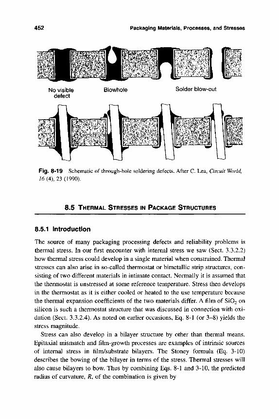
452 Packaging Materials, Processes, and Stresses
No visible defect
Blowhole Solder blow-out
Fig. 8-19 Schematic of through-hole soldering defects. After C. Lea, Circuit World, 76(4X23(1990).
8.5 THERIVIAL STRESSES IN PACKAGE STRUCTURES
8.5.1 Introduction
The source of many packaging processing defects and reliability problems is thermal stress. In our first encounter with internal stress we saw (Sect. 3.3.2.2) how thermal stress could develop in a single material when constrained. Thermal stresses can also arise in so-called thermostat or bimetallic strip structures, con-sisting of two different materials in intimate contact. Normally it is assumed that the thermostat is unstressed at some reference temperature. Stress then develops in the thermostat as it is either cooled or heated to the use temperature because the thermal expansion coefficients of the two materials differ. A film of Si02 on silicon is such a thermostat structure that was discussed in connection with oxi-dation (Sect. 3.3.2.4). As noted on earlier occasions, Eq. 8-1 (or 3-8) yields the stress magnitude.
Stress can also develop in a bilayer structure by other than thermal means. Epitaxial mismatch and film-growth processes are examples of intrinsic sources of internal stress in film/substrate bilayers. The Stoney formula (Eq. 3-10) describes the bowing of the bilayer in terms of the stress. Thermal stresses will also cause bilayers to bow. Thus by combining Eqs. 8-1 and 3-10, the predicted radius of curvature, R, of the combination is given by
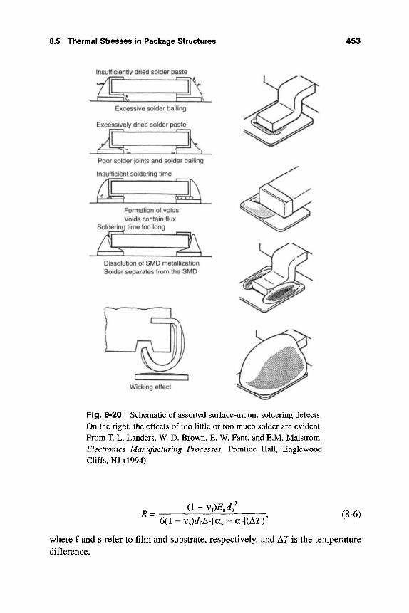
8.5 Thermal Stresses in Package Structures 453
Insufficiently dried solder paste
Excessive solder balling
Excessively dried solder paste
A k, « i I
Poor solder joints and solder balling
Insufficient soldering time
'-^ ^ - * f->
Formation of voids Voids contain flux
Soldering time too long
/ g = ^ Dissolution of SMD metallization Solder separates from the SMD
Wicking effect
Fig. 8-20 Schematic of assorted surface-mount soldering defects. On the right, the effects of too little or too much solder are evident. From T. L. Landers, W. D. Brown, E. W. Fant, and E.M. Malstrom. Electronics Manufacturing Processes, Prentice Hall, Englewood Cliffs, NJ (1994).
R (1 - vdEsd^
6(l-VsK£f[as-af](Ar)' (8-6)
where f and s refer to film and substrate, respectively, and AT is the temperature
difference.
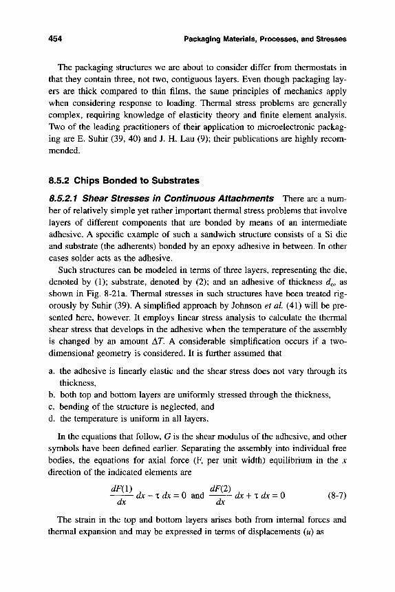
454 Packaging Materials, Processes, and Stresses
The packaging structures we are about to consider differ from thermostats in that they contain three, not two, contiguous layers. Even though packaging lay-ers are thick compared to thin films, the same principles of mechanics apply when considering response to loading. Thermal stress problems are generally complex, requiring knowledge of elasticity theory and finite element analysis. Two of the leading practitioners of their application to microelectronic packag-ing are E. Suhir (39, 40) and J. H. Lau (9); their publications are highly recom-mended.
8.5.2 Chips Bonded to Substrates
8.5.2.1 Shear Stresses in Continuous Attachments There are a num-ber of relatively simple yet rather important thermal stress problems that involve layers of different components that are bonded by means of an intermediate adhesive. A specific example of such a sandwich structure consists of a Si die and substrate (the adherents) bonded by an epoxy adhesive in between. In other cases solder acts as the adhesive.
Such structures can be modeled in terms of three layers, representing the die, denoted by (1); substrate, denoted by (2); and an adhesive of thickness d^, as shown in Fig. 8-2la. Thermal stresses in such structures have been treated rig-orously by Suhir (39). A simplified approach by Johnson et al (41) will be pre-sented here, however. It employs linear stress analysis to calculate the thermal shear stress that develops in the adhesive when the temperature of the assembly is changed by an amount Ar. A considerable simplification occurs if a two-dimensional geometry is considered. It is further assumed that
a. the adhesive is linearly elastic and the shear stress does not vary through its thickness,
b. both top and bottom layers are uniformly stressed through the thickness, c. bending of the structure is neglected, and d. the temperature is uniform in all layers.
In the equations that follow, G is the shear modulus of the adhesive, and other symbols have been defined earlier. Separating the assembly into individual free bodies, the equations for axial force (F, per unit width) equilibrium in the x direction of the indicated elements are
dF{\) dF(2) —-— dx-x dx = 0 and dx + x dx = 0 (8-7)
dx dx
The strain in the top and bottom layers arises both from internal forces and thermal expansion and may be expressed in terms of displacements (M) as
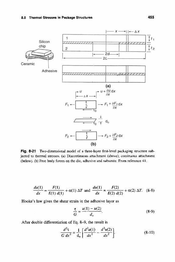
8.5 Thermal Stresses in Package Structures 455
Silicon chip
Ceramic
Adhesive
1 yy/z/z/y^///// \ 2
-<——
X-
* 2c/ • 2L
n
| - ^ A X
y y y / y / .
^
t ' 1'
2ZZZZZZZZZZZZ^ZZZZZZ ,p/ / ///jnrA y / / / / T
(a)
F r + ^ d x 8x
To
^ T ^ o
F2+^2dX ax
(b)
Fig. 8-21 Two-dimensional model of a three-layer first-level packaging structure sub-jected to thermal stresses, (a) Discontinuous attachment (above); continuous attachment (below), (b) Free body forces on the die, adhesive and substrate. From reference 41.
i ! ! ( i ) . _ W _ , „ „ ) ^ ^ ^ , i ! 2 ^ = - m ^ , a ( 2 ) A r . (8-8) dx E(X) d{l) dx E(2) d(2)
Hooke's law gives the shear strain in the adhesive layer as
X «(1) - M(2)
G do
After double differentiation of Eq. 8-9, the result is
d\ Gdx^ do dx' dx'
(8-9)
(8-10)
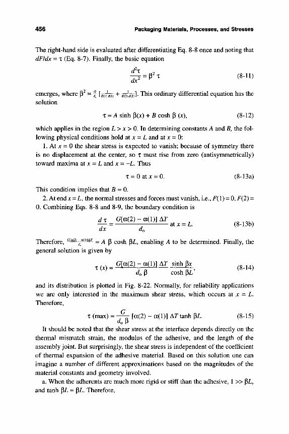
456 Packaging Materials, Processes, and Stresses
The right-hand side is evaluated after differentiating Eq. 8-8 once and noting that dFldx = T (Eq. 8-7). Finally, the basic equation
dx j = p^T (8-11)
emerges, where |3^ = f [i iy ^ + Eaun)^- This ordinary differential equation has the solution
T = A sinh P(jc) + B cosh p (jc), (8-12)
which applies in the region L > ;c> 0. In determining constants A and B, the fol-lowing physical conditions hold at JC = L and at JC = 0:
1. At JC = 0 the shear stress is expected to vanish; because of symmetry there is no displacement at the center, so x must rise from zero (antisymmetrically) toward maxima at JC = L and JC = -L. Thus
T = Oatjc = 0. (8-13a)
This condition implies that B = 0. 2. At end JC = L, the normal stresses and forces must vanish, i.e., F(l) = 0, F(2) =
0. Combining Eqs. 8-8 and 8-9, the boundary condition is
dx G[a(2) - a(l)] Ar
dx do atJc = L. (8-13b)
Therefore, ^"^ " ' ' ^ = A p cosh PL, enabling A to be determined. Finally, the general solution is given by
^ ^ ^ ^ G[a(2) - a(l)] AT sinh p^ ^^_^^^ do P cosh PL'
and its distribution is plotted in Fig. 8-22. Normally, for reliability applications we are only interested in the maximum shear stress, which occurs at jc = L. Therefore,
T (max) = - ^ [a(2) - a(l)] Ar tanh pL. (8-15)
It should be noted that the shear stress at the interface depends directly on the thermal mismatch strain, the modulus of the adhesive, and the length of the assembly joint. But surprisingly, the shear stress is independent of the coefficient of thermal expansion of the adhesive material. Based on this solution one can imagine a number of different approximations based on the magnitudes of the material constants and geometry involved.
a. When the adherents are much more rigid or stiff than the adhesive, 1 » PL, and tanh PL « pL. Therefore,
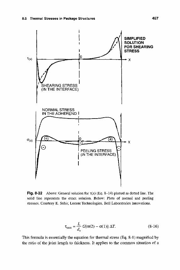
8.5 Thermal Stresses in Package Structures 457
X(x)
^(x)
SHEARING STRESS (IN THE INTERFACE)
NORMAL STRESS INTHEADHEREND I
SIMPLIFIED SOLUTION FOR SHEARING STRESS
*- X
^ X
Fig. 8-22 Above: General solution for T(JC) (Eq. 8-14) plotted as dotted line. The solid line represents the exact solution. Below: Plots of normal and peeling stresses. Courtesy E. Suhir, Lucent Technologies, Bell Laboratories Innovations.
T^.. = — G[a(2)-aa)]AT. (8-16)
This formula is essentially the equation for thermal stress (Eq. 8-1) magnified by the ratio of the joint length to thickness. It applies to the common situation of a
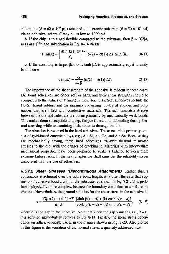
458 Packaging Materials, Processes, and Stresses
silicon die {E = 62 x 10^ psi) attached to a ceramic substrate (£ = 50 x 10^ psi) via an adhesive, where G may be as low as 1000 psi.
b. If the chip is thin and flexible compared to the substrate, then P = {G/[do E(l) rf(l)]}"^ and substitution in Eq. 8-14 yields
T (max) = | - ^ ^ i ^ 4 ^ i ^ l [ a ( 2 ) - a ( l ) ] ArtanhpL. (8-17) (d(l) £(1) G]
c. If the assembly is large, PL » 1, tanh PL is approximately equal to unity. In this case
X (max) = -—-• [a(2) - a(l)] AT. (8-18)
The importance of the shear strength of the adhesive is evident in these cases. Die bond adliesives are either soft or hard, and their shear strengths should be compared to the values of T (max) in these formulas. Soft adhesives include the Pb-Sn based solders and the organics consisting mostly of epoxies and poly-imides that are filled with conductive materials. Thermal mismatch stresses between the die and substrate are borne primarily by mechanically weak bonds. This makes them susceptible to creep, fatigue fracture, or debonding during ther-mal stressing while transmitting little stress to damage the die.
The situation is reversed in the hard adhesives. These materials primarily con-sist of gold-based eutectic alloys, e.g., Au-Si, Au-Ge, and Au-Sn. Because they are mechanically strong, these hard adhesives transmit thermal mismatch stresses to the die, with the danger of cracking it. Materials with intermediate mechanical properties have been proposed to strike a balance between these extreme failure risks. In the next chapter we shall consider the reliability issues associated with the use of adhesives.
8.5.2.2 Shear Stresses (Discontinuous Attachment) Rather than a continuous attachment over the entire bond length, it is often the case that seg-ments of adhesive bond a chip to the substrate, as shown in Rg. 8-21. This prob-lem is physically more complex, because the boundary conditions at jc = J are not obvious. Nevertheless, the general solution for the shear stress in the adhesive is
_ G[a(2) ~ a(l)] AT [sinh f^(x-d) + ^d cosh p(jc - d)]
^ 4 P [cosh P(L - tO + ^d sinh P(L - ^ ] ' ^ " ^
where d is the gap in the adhesive. Note that when the gap vanishes, i.e., d = 0, this solution immediately reduces to Eq. 8-14. Finally, the shear stress depen-dence on adhesive length varies in the manner shown in Fig. 8-23. Also plotted in this figure is the variation of the normal stress, a quantity addressed next.

8.5 Thermal Stresses in Package Structures 459
1.0
0.9
0.8
0.7
0.6
0.5
0.4
0.3
0.2
0.1
W»mmm 7
"x: '
^max .
CToo
max
= tanhpL Too
1 1
cosh pL 1
PL
Fig. 8-23 Shear stress distribution as a function of joint length in adhesively bonded joints. Note: o^ = £(1) [a(2) - a(l)] Ar, t«. = (l/(dop) G[a(2) - a{l)] AT and 2L = joint length. Courtesy E. Suhir, Lucent Technologies, Bell Labora-tories Innovations.
8.5.2.3 Normal and Peeling Stresses In addition to interfacial shear stresses in the adhesive, the adherents are subject to normal and peeling stresses. The normal, or tensile stress acts along the die axis and arises from F(l); it can be simply obtained by integrating t (x) in Eq. 8-7. As shown in Fig. 8-22, these stresses are large in the center and vanish at the outer edges of the chip. In the case of a film attached to a substrate, d(2) » d(l), a simple formula for the max-imum tensile stress in the film is given by Suhir (39):
a (max) = -£{!) [a(2) - a(l)] AT 1 1
cosh pL (8-20)
while stresses in the substrate are only d(l)/d(2) times as large. The transverse normal, or peeling, stresses arise from the constraint that
forces the assembled components to bend jointly and have the same curvature at all sections despite differences in their flexural rigidities (i.e., E d^/12). An explicit simplified formula for the peeling stress (Op) distribution is given by
460 Packaging Materials, Processes, and Stresses
|LiG[a(2) - a(l)] Ar coshpx cJpW = -
In this formula,
cTpW = - :, r ^ . (8-21) do cosh p L
d(2) E(l) d(l)^ d(l) E(2) d{2f
\^ = 12 [1 -v(l)^] 12 [1 -v{2f]
E{\) d(lf E(2) d(2f
6 [ l - v ( l ) ' ] 6 [ l - v ( 2 ) ^ ]
reflecting the difference in adherent thicknesses and flexural rigidities. Peeling stresses are small everywhere except at the extreme edges of the attachment (Fig. 8-22).
As an illustrative example, the three relevant stresses were calculated for the case of a GaAs MMIC power amplifier device (42), and the results are plotted in Fig. 8-24. Using a value of AT equal to 345°C, the maximum tensile stress in the GaAs die is found to be 7.36 MPa, the maximum shear stress in the Au-Ge adhe-sive is 1.8 MPa, and the peeling stress at the edge of the substrate (CM 15 or 15%Cu-85%Mo) is only 0.22 MPa.
8.5.3 Thermal Stress in Other Structures
With slight modification, the basic analysis of thermal stress has been applied to other than planar semiconductor/adhesive/substrate assemblies. Stress in various wirebond configurations and attachments used in ceramic packages are among the examples briefly described next.
8.5.3.1 Wirebonds In the case of wirebonds, the Al bonding pad on a chip was assumed by Hu et al. (43) to act something like an adhesive between the wire above and the semiconductor substrate beneath. The equation derived for the shear stress in the bond pad is given by
T(X) ^ ^ E(s)A(s) J cosh yL(w)
E(p)A(p)
The symbols w, /?,and s refer to wire, pad, and substrate quantities, respectively, and Yis defined by 7 = (Gp/bp) {r/[E(vj) A(w)] + w(p)/[E(s) A(s)]}\ in addition, r is the wire radius, and A, L, and w are the indicated cross-sectional area, length, and width dimensions, respectively. A more complex expression than Eq. 8-14
8.5 Thermal Stresses in Package Structures 461
• ^ — • — • — •
Normal stress in die
Siiear stress in interface
Peeling stress in interface
-m—^1^-
-2.5 -1.5 -0.5
Distance to Die Center (mm)
Fig. 8-24 Calculated shear and normal stresses in the substrate of a MMIC power amplifier device composed of GaAs substrate with dimensions 4.7 x 2.7 x 0.1 mm , Au-Ge eutectic attachment with dimensions 4.7 x 2.7 x 0.0254 mm , and CM 15 (15%Cu-85%Mo) case with dimensions 14.4 x 12.7 x 2.8 mml From J. M. Hu, in Reliability of Gallium Arsenide MMICs, ed. A. Christou, J. Wiley and Sons, Chich-ester (1992).
results because the geometry is more involved. Nevertheless, the spatial distrib-ution of the stress in this solution is essentially the same.
8.5.3,2 Sealing Ceramic Pacliages Low-melting solder glass is used to seal metal-to-ceramic and ceramic-to-ceramic joints in high-performance ceramic packages. There are two critical areas that must be sealed for the package to be hermetic. The first is the metal leadframe, which is sealed on both sides to the ceramic base with a layer of solder glass. Similarly, at the top of the package a metal-metal welded or soldered seam joins the ceramic lid to the base. Glass is inherently brittle, and therefore the thermal expansion mismatch between the
462 Packaging Materials, Processes, and Stresses
glass and lead frame as well as between glass and ceramic is of concern. However, since the lead frame is thin, its contribution to the stress of the glass layer is small, and thus only the ceramic-glass-ceramic structure is of interest.
A formula derived (44) for the maximum normal stress in a very wide glass layer is
_E(g)[a(c)-a(g)](T-T,)
^^dig)Eig)
d{c) E(c)
(8-23)
where g and c refer to the glass and ceramic, d represents the total thickness of the involved glass or ceramic parts, and all moduli are reduced by the appro-priate (1 - v) factor; i.e., E(i) = E/[l - v(0]. Frequently, d(c) > d(g), and
a = E(g) [a(c) - a(^)] (T - T,) (8-24)
is the simple and conservative solution.
Example 8-1 Consider a ceramic package where the solder glass used has the following properties; E(g) = 0.7 x 10^ kg/cm^ v (g) = 0.27, a(^) = 6.8 x 10"^ ''C"^ Similarly, for the alumina ceramic, E (c) = 3.5 x 10^ kg/cm^, v (c) = 0.25, a(c) = 7.2 X 10"^ °C"^ If the seal processing temperature is 450°C, what stress can be expected in the glass at 25''C?
Answer It is assumed that all stresses are relieved at 450°C. Therefore, by Eq. 8-24 the thermal stress produced in the glass at 25°C is a = 0.7 x 10^/(1 - 0.27) [7.2 X 10"^ - 6.8 X 10^] (450 - 25) = 163 kg/cml This value should be compared to the 5500 kg/cm^ compressive (fracture) strength of the glass. The undesirable tensile stress that develops underscores the need for high-toughness solder glasses.
8.5.3.3 Thermal Stresses in Solder Joint Structures—Case Histories As final examples of thermal stresses in packaging let us consider a couple of case histories. In the first, strains were experimentally measured in a solder-ball-grid array employing Moir^ interferometry techniques (45). The overall structure shown in Fig. 8-25a consisted of a heat sink bonded to a ceramic package, which was in turn soldered to a PCB via the ball-grid array. Upon cooling this structure from 60°C to room temperature all of the associated components contracted. As a result, the fringe pattern reproduced in Figs. 8-25b and 8-25c was obtained, corresponding to relative material displacements (strains) in the horizontal (x) and vertical (y) directions. Since the deformation magnitude and direction are
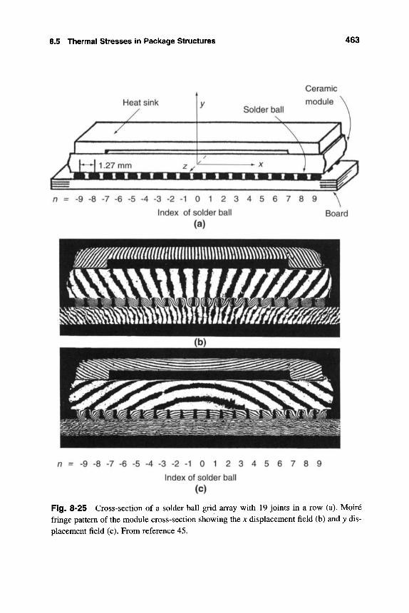
8.5 Thermal Stresses in Package Structures 463
Heat sink
Ceramic
module
n = -9 -8 -7 -6 -5 -4 -3 -2 -1 0 1 2 3 4 5 6 7 8 9 "^
Index of solder ball Board (a)
n = -9 -8 -7 -6 -5 -4 - 3 - 2 - 1 0 1 2 3 4 5
Index of solder ball
(c)
6 7 8 9
Fig. 8-25 Cross-section of a solder ball grid array with 19 joints in a row (a). Moire fringe pattern of the module cross-section showing the x displacement field (b) and y dis-placement field (c). From reference 45.
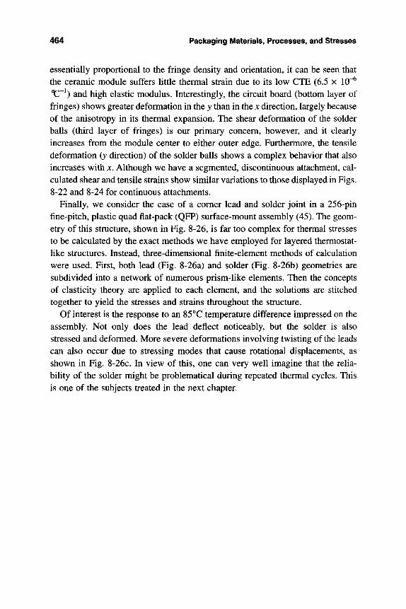
464 Packaging Materials, Processes, and Stresses
essentially proportional to the fringe density and orientation, it can be seen that the ceramic module suffers little thermal strain due to its low CTE (6.5 x 10"^ XT^) and high elastic modulus. Interestingly, the circuit board (bottom layer of fringes) shows greater deformation in the y than in the x direction, largely because of the anisotropy in its thermal expansion. The shear deformation of the solder balls (third layer of fringes) is our primary concern, however, and it clearly increases from the module center to either outer edge. Furthermore, the tensile deformation (y direction) of the solder balls shows a complex behavior that also increases with x. Although we have a segmented, discontinuous attachment, cal-culated shear and tensile strains show similar variations to those displayed in Figs. 8-22 and 8-24 for continuous attachments.
Finally, we consider the case of a comer lead and solder joint in a 256-pin fine-pitch, plastic quad flat-pack (QFP) surface-mount assembly (45). The geom-etry of this structure, shown in Fig. 8-26, is far too complex for thermal stresses to be calculated by the exact methods we have employed for layered thermostat-like structures. Instead, three-dimensional finite-element methods of calculation were used. First, both lead (Fig. 8-26a) and solder (Fig. 8-26b) geometries are subdivided into a network of numerous prism-like elements. Then the concepts of elasticity theory are applied to each element, and the solutions are stitched together to yield the stresses and strains throughout the structure.
Of interest is the response to an 85°C temperature difference impressed on the assembly. Not only does the lead deflect noticeably, but the solder is also stressed and deformed. More severe deformations involving twisting of the leads can also occur due to stressing modes that cause rotational displacements, as shown in Fig. 8-26c. In view of this, one can very well imagine that the relia-bility of the solder might be problematical during repeated thermal cycles. This is one of the subjects treated in the next chapter.
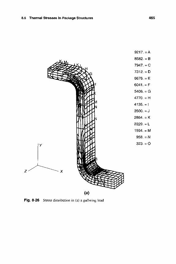
8.5 Thermal Stresses in Package Structures 465
9217. = A
8582. = B
7947. = C
7312. = D
6676. = E
6041. = F
5406. = G
4770. = H
4135. = I
3500. = J
2864. = K
2229. = L
1594. = M
958. = N
323. = O
Fig. 8-26 Stress distribution in (a) a guUwing lead
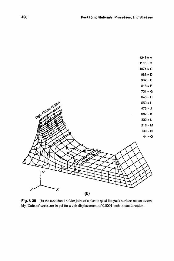
466 Packaging Materials, Processes, and Stresses
Fig. 8-26 (b) the associated solder joint of a plastic quad flat pack surface-mount assem-bly. Units of stress are in psi for a unit displacement of 0.0001 inch in one direction.
Exercises 467
Fig. 8-26 An example of thermal distortion in the joint is shown in (c) From reference 46.
EXERCISES
-1 A 5-chip multichip module consists of one microprocessor, 2 ASIC (appli-cation-specific IC) and 2 memory chips with respective yields of 92%, 83%, and 97%. What is the expected yield of the MCM?
-2 Both large and small dielectric constant materials are required for various electrical functions discussed in this book. Give an example of each.
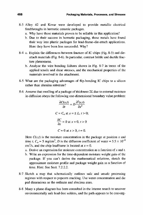
468 Packaging Materials, Processes, and Stresses
8-3 Alloy 42 and Kovar were developed to provide metallic electrical feedthroughs in hermetic ceramic packages. a. Why have these materials proven to be reliable in this application? b. Due to their success in hermetic packaging, these metals have found
their way into plastic packages for lead-frame-die-attach applications. Here they have been less successful. Why?
8-4 a. Explain the differences between fracture of IC chips (Fig. 8-5) and die-attach materials (Fig. 8-6). In particular, contrast brittle and ductile frac-ture phenomena,
b. Analyze the wire bonding failures shown in Fig. 8-7 in terms of the applied tensile and shear stresses, and the mechanical properties of the materials involved in the attachment.
8-5 What are the packaging advantages of flip-bonding IC chips to a silicon rather than alumina substrate?
8-6 Assume that swelling of a package of thickness 2L due to external moisture in-diffusion obeys the following one-dimensional boundary value problem:
dC{x,t) d\xj) dt ~ dx^
C = Co at jc = ± L, r > 0;
-z— = 0 2iix = 0,t>0 ax
C = 0 at jc> 0, r = 0.
Here C(x,t) is the moisture concentration in the package at position x and time t, Co = 5 mg/cm^, D is the diffusion coefficient of water = 5.5 x 10"^ cm^/s, and the chip-leadframe is located at x = 0. a. Derive an expression for moisture concentration as a function of jc and t. b. Write an expression for the time-dependent moisture weight gain of the
package. If you can't derive the mathematical solutions, sketch the approximate moisture profile and package weight gain as a function of time. Hint: See Sect. 7.2.2.2.
8-7 Sketch a map that schematically outlines safe and unsafe processing regimes with respect to popcorn cracking. Use water concentration and die pad dimensions as the ordinate and abscissa axes.
8-8 Many a phase diagram has been consulted in the intense search to uncover environmentally safe lead-free solders, and the path appears to be converg-
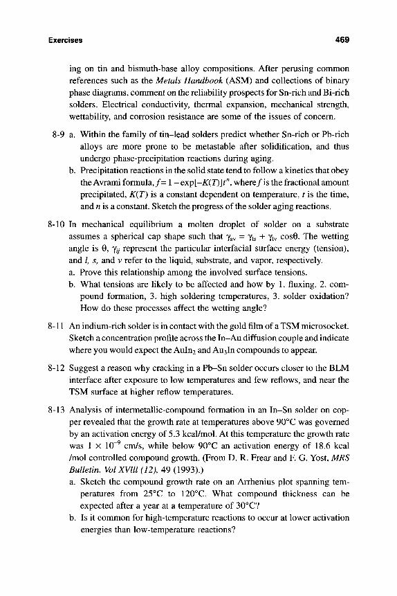
Exercises 469
ing on tin and bismuth-base alloy compositions. After perusing common references such as the Metals Handbook (ASM) and collections of binary phase diagrams, comment on the reliability prospects for Sn-rich and Bi-rich solders. Electrical conductivity, thermal expansion, mechanical strength, wettability, and corrosion resistance are some of the issues of concern.
8-9 a. Within the family of tin-lead solders predict whether Sn-rich or Pb-rich alloys are more prone to be metastable after solidification, and thus undergo phase-precipitation reactions during aging,
b. Precipitation reactions in the solid state tend to follow a kinetics that obey the Avrami formula,/= 1 - &xp[-K(T)]t^, where/is the fractional amount precipitated, K(T) is a constant dependent on temperature, t is the time, and w is a constant. Sketch the progress of the solder aging reactions.
8-10 In mechanical equilibrium a molten droplet of solder on a substrate assumes a spherical cap shape such that y^^ = yis + yiv cosG. The wetting angle is 0, Y// represent the particular interfacial surface energy (tension), and /, s, and v refer to the liquid, substrate, and vapor, respectively. a. Prove this relationship among the involved surface tensions. b. What tensions are likely to be affected and how by 1. fluxing, 2. com-
pound formation, 3. high soldering temperatures, 3. solder oxidation? How do these processes affect the wetting angle?
8-11 An indium-rich solder is in contact with the gold film of a TSM microsocket. Sketch a concentration profile across the In-Au diffusion couple and indicate where you would expect the Auln2 and Au3ln compounds to appear.
8-12 Suggest a reason why cracking in a Pb-Sn solder occurs closer to the BLM interface after exposure to low temperatures and few reflows, and near the TSM surface at higher reflow temperatures.
8-13 Analysis of intermetallic-compound formation in an In-Sn solder on cop-per revealed that the growth rate at temperatures above 90°C was governed by an activation energy of 5.3 kcal/mol. At this temperature the growth rate was 1 X 10"^ cm/s, while below 90°C an activation energy of 18.6 kcal /mol controlled compound growth. (From D. R. Frear and F. G. Yost, MRS Bulletin, Vol XVlll (12), 49 (1993).) a. Sketch the compound growth rate on an Arrhenius plot spanning tem-
peratures from 25°C to 120°C. What compound thickness can be expected after a year at a temperature of 30°C?
b. Is it common for high-temperature reactions to occur at lower activation energies than low-temperature reactions?
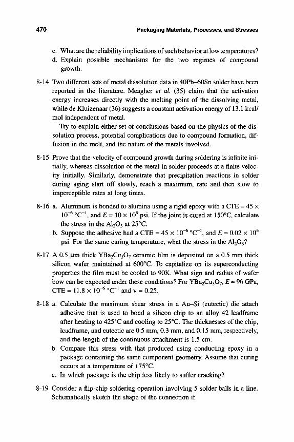
470 Packaging Materials, Processes, and Stresses
c. What are the reliabihty impHcations of such behavior at low temperatures? d. Explain possible mechanisms for the two regimes of compound
growth.
8-14 Two different sets of metal dissolution data in 40Pb-60Sn solder have been reported in the literature. Meagher et al (35) claim that the activation energy increases directly with the melting point of the dissolving metal, while de Kluizenaar (36) suggests a constant activation energy of 13.1 kcal/ mol independent of metal.
Try to explain either set of conclusions based on the physics of the dis-solution process, potential complications due to compound formation, dif-fusion in the melt, and the nature of the metals involved.
8-15 Prove that the velocity of compound growth during soldering is infinite ini-tially, whereas dissolution of the metal in solder proceeds at a finite veloc-ity initially. Similarly, demonstrate that precipitation reactions in solder during aging start off slowly, reach a maximum, rate and then slow to imperceptible rates at long times.
8-16 a. Aluminum is bonded to alumina using a rigid epoxy with a CTE = 45 x 10"^ °C"\ and j ^ = 10 x 10^ psi. If the joint is cured at 150°C, calculate the stress in the AI2O3 at 25°C.
b. Suppose the adhesive had a CTE = 45 x 10"^ °C"\ and E = 0.02 x 10^ psi. For the same curing temperature, what the stress in the AI2O3?
8-17 A 0.5 |xm thick YBa2Cu307 ceramic film is deposited on a 0.5 mm thick silicon wafer maintained at 600°C. To capitalize on its superconducting properties the film must be cooled to 90K. What sign and radius of wafer bow can be expected under these conditions? For YBa2Cu307, E = 96 GPa, CTE = 11.8 X 10"^ °C-^ and v = 0.25.
8-18 a. Calculate the maximum shear stress in a Au-Si (eutectic) die attach adhesive that is used to bond a silicon chip to an alloy 42 leadframe after heating to 425°C and cooling to 25°C. The thicknesses of the chip, leadframe, and eutectic are 0.5 nmi, 0.3 nmi, and 0.15 mm, respectively, and the length of the continuous attachment is 1.5 cm.
b. Compare this stress with that produced using conducting epoxy in a package containing the same component geometry. Assume that curing occurs at a temperature of 175°C.
c. In which package is the chip less likely to suffer cracking?
8-19 Consider a flip-chip soldering operation involving 5 solder balls in a line. Schematically sketch the shape of the connection if
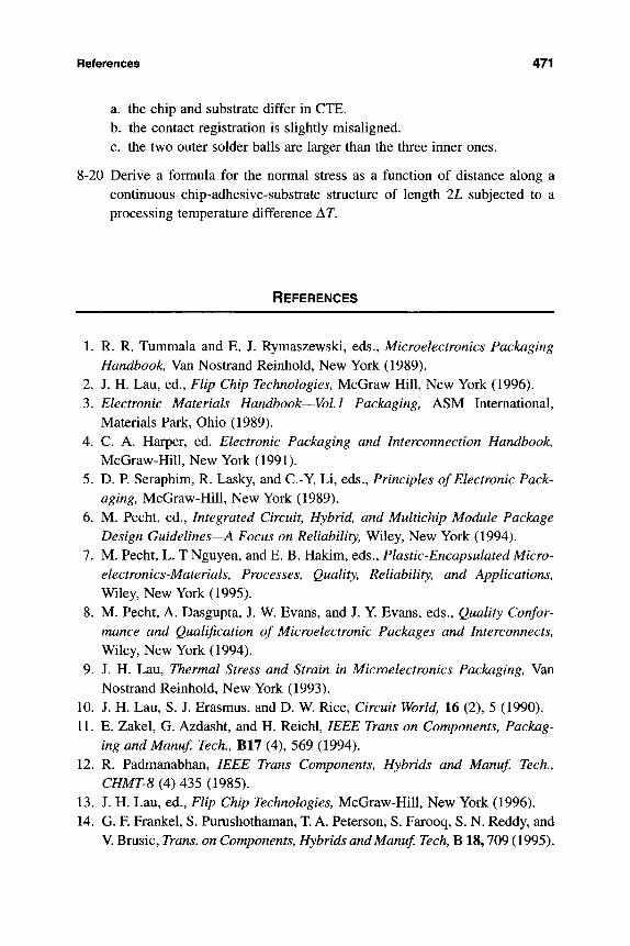
References 471
a. the chip and substrate differ in CTE. b. the contact registration is slightly misaligned. c. the two outer solder balls are larger than the three inner ones.
8-20 Derive a formula for the normal stress as a function of distance along a continuous chip-adhesive-substrate structure of length IL subjected to a processing temperature difference AT.
REFERENCES
1. R. R. Tummala and E. J. Rymaszewski, eds., Microelectronics Packaging Handbook Van Nostrand Reinhold, New York (1989).
2. J. H. Lau, ed., Flip Chip Technologies, McGraw Hill, New York (1996). 3. Electronic Materials Handbook—Vol.1 Packaging, ASM International,
Materials Park, Ohio (1989). 4. C. A. Harper, ed. Electronic Packaging and Interconnection Handbook,
McGraw-Hill, New York (1991). 5. D. R Seraphim, R. Lasky, and C.-Y. Li, eds.. Principles of Electronic Pack-
aging, McGraw-Hill, New York (1989). 6. M. Pecht, ed.. Integrated Circuit, Hybrid, and Multichip Module Package
Design Guidelines—A Focus on Reliability, Wiley, New York (1994). 7. M. Pecht, L. T Nguyen, and E. B. Hakim, eds., Plastic-Encapsulated Micro-
electronics-Materials, Processes, Quality, Reliability, and Applications, Wiley, New York (1995).
8. M. Pecht, A. Dasgupta, J. W. Evans, and J. Y. Evans, eds.. Quality Confor-mance and Qualification of Microelectronic Packages and Interconnects, Wiley, New York (1994).
9. J. H. Lau, Thermal Stress and Strain in Microelectronics Packaging, Van Nostrand Reinhold, New York (1993).
10. J. H. Lau, S. J. Erasmus, and D. W. "Rict, Circuit World, 16 (2), 5 (1990). 11. E. Zakel, G. Azdasht, and H. Reichl, IEEE Trans on Components, Packag-
ing and Manuf Tech., B17 (4), 569 (1994). 12. R. Padmanabhan, /EEE Trans Components, Hybrids and Manuf Tech.,
CHMT-8 (4) 435 (1985). 13. J. H. Lau, ed.. Flip Chip Technologies, MCGTSLW-HUI New York (1996). 14. G. F. Frankel, S. Purushothaman, T. A. Peterson, S. Farooq, S. N. Reddy, and
V. Brusic,Tran^. on Components, Hybrids and Manuf Tech, B 18,709 (1995).
472 Packaging Materials, Processes, and Stresses
15. L. T. Manzione, Plastic Packaging of Microelectronic Devices, Van Nos-trand Reinhold, New York (1990).
16. K. N. Ritz, W. T. Stacy, and E. K. Broadbent, 25th Annual Proceedings of the IEEE Reliability Physics Symposium, p. 28, (1987).
17. E. Suhir and L. T. Manzione, J. Electronic Packaging, Trans ASME, 113, 421 (1991).
18. E. Suhir and L. T. Manzione, J. Electronic Packaging, Trans ASME, 113, 16 (1991).
19. A. A. Gallo and R. Munamarty, IEEE Trans, on Reliability, 44 (3), 362 (1995).
20. R. Shook and T. Conrad, Tutorial Notes, IEEE International Reliability Physics Symposium, 1.1 (1995).
21. S. K. Groothuis, K. G. Heinen, and L. Rimpillo, 33rd Annual Proceedings of the IEEE Reliability Physics Symposium, p. 76 (1995).
22. M. R. Lin and J. T. Yue, 25th Annual Proceedings of the IEEE Reliability Physics Symposium, p. 164 (1987).
23. J. H. Lau, ed. Chip on Board Technologies for Multicip Modules, Van Nos-trand Reinhold, New York (1994).
24. N. Sherwani, Q. Yu, and S. Badida, Introduction to Multicip Modules, Wiley, New York (1995).
25. H. H. Manko, Solders and Soldering, 2nd. Ed, McGraw Hill, New York (1979). 26. A. Rahn, The Basics of Soldering, Wiley, New York (1993). 27. J. H. Lau, ed., Solder Joint Reliability, Van Nostrand Reinhold, New York
(1991). 28. W. B. Hampshire, Soldering and Surface Mount Tech., 14 (6), 49 (1993). 29. H. J. Frost, in Solder Joint Reliability, ed. J. H. Lau, Van Nostrand Reinhold,
New York (1991). 30. R. Darveaux and K. Banerji, IEEE Trans.Components, Hybrids and Manuf.
Tech. 15, 1013 (1992). 31. J. A. DeVore, J. of Metals, p. 51, July (1984). 32. L. J. Turbini and D. Cauffield, Soldering and Surface Mount Tech., 17 (6),
30 (1994). 33. B. N. Ellis, Circuit World, 20 (4), 26 (1994). 34. B. Meagher, D. Schwarcz, and M. Ohring, J. Mat. ScL, 31, 5479 (1996). 35. E. E. de Kluizenaar, Philips Electron Optics Bulletin 131, 3 (1991). 36. K. J. Puttlitz, IEEE Trans. Components, Hybrids and Manuf. Tech. 13 (4),
647 (1990). 37. R. Prasad, Semicond. Int. 19 (4), 116 (1996). 38. A. Malhotra, in M. Pecht, ed.. Soldering Processes and Equipment, Wiley,
New York (1993).
References 473
39. E. Suhir in Advances in Thermal Modeling of Electronic Components and Systems Vol. 1, ed. by A. Bar-Cohen and A. D. Kraus, Hemisphere, New York (1988).
40. E. Suhir, MRS Symp. Proc. Electronic Packaging Mat. Sci.-IL, 133 (1986). 41. E. A. Johnson, W. T. Chen, and C. K. Lim, in Principles of Electronic Pack-
aging, ed. D. P. Seraphim, R. Lasky, and C.-Y. Li, McGraw-Hill, New York (1989).
42. J. M. Hu, in Reliability of Gallium Arsenide MMICs, ed. A. Christou, Wiley, Chichester (1992).
43. J. M. Hu, M. Pecht, and A. Dasgupta, /. Electronic Packaging, Trans ASME, 113, 275 (1991),
44. E. Suhir and B. Poborets, /. Electronic Packaging, Trans ASME, 112, 204 (1990).
45. Y Guo, C. K. Lim, W. T. Chen, and C. G. Woychik, IBM J. Res. and Develop., 37, 635 (1993).
46. J. H. Lau in Thermal Stress and Strain in Microelectronics Packaging, ed. J. H. Lau, Van Nostrand Reinhold, New York (1993).

This Page Intentionally Left Blank
Chapter 9
Degradation of Contacts and Package Interconnections
9.1 INTRODUCTION
The unifying theme of this chapter encompasses problems that arise in main-taining electrical continuity between conductors. We have all instinctively diag-nosed poor contacts as the source of malfunction in some piece of electrical equipment or other, and often been correct. In the days before transistors, the simple act of making a local telephone call activated hundreds of electro-mechanical contacts, whose inefficient operation or malfunction meant signal distortion, noise, or even lack of signal transmission. Whether they are "static," as in permanent soldered interconnections, or are "dynamic," sliding and rotat-ing, as in switches and motors, electrical contacts pose a variety of interesting and important reliability problems.
In this chapter we will discuss both types of contacts, starting with a classical treatment of the nature of contacting, current-carrying conductors. Dynamic con-tact problems arising from mechanical wear, corrosion, and stress relaxation are among the first reliability issues we will address. Much of the chapter's later focus, however, will be devoted to the reliability of solder materials used in interlevel packaging connections. In this sense the chapter continues the discus-sion that began in Chapter 8 dealing with packaging configurations, joining tech-niques, and solder defects.
475
476 Degradation of Contacts and Package Interconneetions
Building on the previously developed thermal-stress analyses, failure model-ing of contacts and solder interconnections is possible, at least in principle. Nev-ertheless, it still remains a formidable task to obtain estimates for contact failure times because
1. stress or strain levels required to cause failure are often unknown; 2. the applied stresses are usually cyclic in nature; 3. component contact and structural geometries are complex; 4. contacting surfaces may wear due to the relative motion between them; and 5. the elevated temperature plastic and viscoelastic behavior of the involved
materials often displays a complex temperature-time-environment history.
When applied to solder interconnections, a logical failure-modeling approach first assumes the operative thermal stress levels expected as calculated previously. The cyclic nature of the stressing must then be considered and this information fended together with material properties into the relevant expressions that describe the deformation response. Creep, fatigue, and fracture are the operative mecha-nisms that cause packaging components and structures to fail. These important subjects are basically the substance of two of the later chapter sections.
Finally, there is a discussion of vibration and dynamic loading effects. In addition to static and cyclic differential thermal-expansion effects, dynamic loading and vibration can also be quite harmful from the standpoint of equip-ment reliability. Because of potential fatigue damage to soldered leads due to vibratory flexure of circuit boards and components, the subject is treated in this chapter.
9.2 THE NATURE OF CONTACTS
9.2.1 Scope
The purpose of electrical contacts is threefold: to make or complete a circuit, to maintain current flow through the circuit, and to break or open the circuit when required. Contacts must reliably repeat these functions over specified time inter-vals that may be as short as a fraction of a millisecond. The electrical spectrum of contacting devices and methods includes switches of all kinds, relays, pin and socket connectors, as well as solder contacts. Although there is considerable overlap, applications may be broadly classified according to their power usage as follows:
9.2 The Nature of Contacts 477
1. power engineering, where high voltages and currents are involved; 2. medium power, with moderate voltages and currents, as in home appliances;
and 3. low voltage-low current applications, as in telecommunications and computers.
In these applications, electrical continuity is often achieved mechanically through impact, sliding, or rotational motion of metal surfaces that are forced together to make and sustain contact. Different mechanical phenomena are involved in each of these domains of usage, and the corresponding contact-fail-ure mechanisms reflect this. In the first category, for example, electrical dis-charges and arcs may be operative, causing extensive erosion and wear of the contacting metal-surfaces. Contacts also degrade by mechanical wear in medium and low-power applications, where in addition, contact opening and closing causes insulating surface films to form as a result of (dry) oxidation or (wet) cor-rosion. In such cases, contact unreliability arises through destruction of the ini-tially smooth contacting and conducting surfaces. The legacy is open and noisy or intermittent electrical behavior.
There is considerable literature on the subject of contacts (1, 2). Investigations continue to be carried out on contact problems, where for over 40 years there has been an annual IEEE Holm Conference on Electrical Contacts, so named for R. Holm, a prominent researcher in this field. In these conference proceedings, also published in the IEEE Transactions on Components, Hybrids and Manufactur-ing Technology, many papers are devoted to damage of high-power contacts, a subject we will not discuss further. Instead, the subsequent treatment will be lim-ited to low- and medium-power contacts, the involved materials, and the degra-dation and reliability issues that surround them.
9.2.2 Constriction Resistance
Consider the physics of what happens when two nominally identical smooth metals contact one another. Although there appears to be contact over a substan-tial area, actual contact is made at a limited number of microscopically small areas. (If the involved metals were infinitely hard, there would be only three points of contact.) With analytical tools such as the scanning electron micro-scope and atomic force microscope, we now know that even very finely polished metal surfaces exhibit arrays of protruding surface asperities separated by val-leys, with peak-to-peak height differences of perhaps 10 nm.
When a potential difference is applied across touching asperity-free cylindri-cal conductors, the current flow lines are parallel, as shown in Fig. 9-la. The contact voltage (Vc) that develops between points A and B is simply given by Ohm's law; i.e., Ve = i o» where i is the current and R^ is the metal ohmic resis-
478 Degradation of Contacts and Package Interconnections
tance. This situation is approximated by a soldered joint because the soHdified solder effectively fills the spaces between asperities. However, when contact occurs only at asperities, current flows in the constricted manner of Fig. 9-lb, distorting the flow lines. The contact voltage (Vc) developed is now larger in order to maintain the same current and is given by
Ve = i (Ro + RcX (9-1)
where Re is the the so-called constriction resistance. Analogy to fluid flow through a constricted pipe under a fixed pressure head (constant Vc) means a smaller throughput (/), which is caused by the added resistance (Re). If, in addi-tion, there is a resistance contribution Rf due to a surface film at the contact, it is added to R^ + R^.
Using concepts of electromagnetic theory it has been shown that when two plane surfaces make contact over an asperity area of radius a, the total constric-tion resistance is
(9-2)
A
B
f > f \ r \ < \
1
f ^ f \
0
(a) (b)
Fig. 9-1 (a) Parallel current flow lines over a large asperity-free area of contact, (b) Constricted current flow lines at contact asperities.
9.2 The Nature of Contacts 479
where p is the resistivity. For metals we recall that p « 10"^ to 10"^ Q. -cm, and, we note that if a is large, Re is negligible; but if a is sufficiently small, R^ can rise to unacceptable levels and cause circuit malfunction.
9.2.3 Heating Effects
One might imagine currents to cause appreciable local heating effects at the asperity-asperity contact welds, known as a-spots, because of the small areas involved. Then the contact resistance would rise from R^l) at temperature T(l) to Re(2) at T(2) according to the relation R^il) = R^il) {1 -h a [T(2) - 7(1)]}, where a is the temperature coefficient of resistivity. Assuming that no heat is lost from the hot contact constriction and that steady-state temperatures are quickly reached, it is not hard to roughly estimate the temperature rise, T(2) - T(l). The power generated from Joule heating {V^IR^ is converted into an equivalent heat (power) flow (K[r(2) - 7(1)] Ac/Ax), where Ac and Ax are the constriction area and length, respectively, and K is the thermal conductivity. Noting that Rc = p Ac/Ac, and equating the two power contributions, the approximate expression
Ve' = P K [T{2) - 7(1)] (9-3)
emerges. In metals the electrical conductivity (a = 1/p) and thermal conductiv-ity are proportional to each other through the formula, pK = LT, where L is the Lorenz number (Sect. 5.5.3). If T is assumed to be some mean temperature between 7(1) and 7(2), then Vl = £T[T(2) - 7(1)]. A more accurate expression (3) is
Ve = 4£[T\2) - T\l)l (9-4)
To see the implications of this formula, let us assume Vc = 1V and 7(1) = 300K. Taking £ = 2.44 x 10"^ W-Q/K^ 7(2) is calculated to be 3200K, a value much higher than the melting point of almost all metals. The mere hint of such high temperatures implies sources of reliability problems. If, for example, the contact area at asperities were 10"^ cm^, the current density would be sufficiently high for electromigration damage to occur; and if contact tarnish films existed, they would probably not survive the heat generated.
9.2.4 Mass Transport Effects at Contacts
The unusually high temperatures and electric current densities present at contact spots mean that at least three different atomic mass transport mechanisms may be operative to transfer material from one contact metal to the other (4). Diffu-sion, electromigration, and thermomigration are the mechanisms, and they are explored in this section.
480 Degradation of Contacts and Package Interconnections
a. Diffusion The diffusional flux of atoms (7a) in a concentration gradient (dC/dx) driving force, with x normal to the contact surface, is a subject treated in this book on at least two prior occasions. Because a discontinuous concentra-tion gradient exists for atoms at a contact junction between two different metals, the mass flux given by
Jra = -D^. (5-1)
is potentially large. For appreciable interdiffusion to occur, the diffusivity given by D = D^Qxp [-ED/RT] must be sufficiently large, and this requires a high tempera-ture. Even if both contacting metals are identical, atomic diffusion is possible. In this case the driving force is the surface-energy gradient that stems from differences in surface curvature. Atoms at asperity tips will tend to diffuse into the valleys and lower the overall surface area. Essentially the same mechanism that is operative during the sintering of metal powder compacts is active here. Sintering or welding at hot spots effectively widens the contact area and reduces the contact resistance.
b. Electromigration It was previously shown that the electromigration flux (/e) is given by
^ ^ ^ C D ^ £ i . ,5.20,
Just as on the chip level at metal-semiconductor interfaces, electromigration at contacts often represents a severe mass-flux divergence. Electromigration mass-transport effects are also expected to be narrowly confined to the contact inter-face where the current density (/e) is large and the temperature high. Further away the conductor widens lowering y'e as well as the temperature. An important term in Eq. 5-20 is the effective valence Z* whose value may range widely in magnitude, i.e., from 5 to -50. Measurement has shown that Z* decreases slowly with increasing temperature.
c. Thermomigration Mass transport driven by temperature gradients is known as thermomigration. The corresponding flux /th is given by
CQ'^D dT RT^ dx' Jih = --^^—^ (9-5)
where Q* is the heat of transport for the element in question. A positive value for g* implies atom migration to colder regions.
The ratio of the electro- to thermo-migration fluxes is given by
A 2:*^p7e Jth -{Q'^IT) dT/dx
and simply represents a ratio of the two generalized forces.
(9-6)
9.2 The Nature of Contacts 481
Example 9-1 Assuming representative values of Z* = -10, (g* = 10 kJ/mol, 7e = 1 X 10^^ A/m^ p = 1 X 10"^ Q-m, T= lOOOK and dT/dx = lO' K/m, does elec-tromigration or thermomigration dominate?
Answer Substituting in Eq. 9-6 we have
Jc -10 X 1.6 X 10"^^ X 1 X 10"^ X 1 X 10^^ X 6.02 x 10^ /th -(10,000/1000) X 10^
9.6.
(Note that to make units match, Avogadro's number must be included in the numerator.) This calculation suggests that electromigration dominates thermo-transport.
Without knowing the temperature distributions and material constants in a contact it is sometimes easier to make measurements. This was done by Runde et al (5), who deposited minute quantities of radioactive zinc on one of two alu-minum contact electrodes. A buildup of Zn observed on the counter electrode, consistent with the current polarity, demonstrated that electromigration had occurred. Transfer of metal at contacts changes the alloy composition and gen-erally raises R^,
9.2.5 Contact Force
Applied force or pressure is required to insure that low-resistance electrical con-tact is made and then sustained. We have already seen that contact resistance depends on the contact area. Since contact heating can potentially alter the area through local mass transfer and/or melting, the relationships among contact resistance, force, and temperature are critical to an understanding of contact per-formance; what is required is a combination of a few simple definitions and for-mulas.
Let us first consider hardness H, a property measured in stress units of N/m^, or commonly kg/mm^. Hardness is essentially a measure of a material's ability to withstand penetration by a harder indenter that is pressed into its surface with normal load P. For a spherical indenter, the hardness is often defined as the load per projected area of diameter d, or H = APIndF. We know, however, that the true mechanical bearing area is but a small fraction of the nominal contact area. As a result, the asperity contacts are subjected to large pressures even with small loads. To account for normal contacts at multiple asperities, the hardness for-mula is modified to
AP H = — ^ , (9-7)
mid where n is the number of such contact points or spots, and d is the average spot diameter. Reconsidering the constriction resistance, it is apparent that
482 Degradation of Contacts and Package Interconnections
R. = -^. (9-8)
This formula assumes that the resistor spots are effectively connected in parallel. Eliminating d between the last two equations yields
with the expected result that the contact resistance decreases as the load increases. This equation holds when P is relatively large and the contact metal deforms plastically. However, when P is small such that the average pressure is roughly less than H/3, the contact deforms elastically; in this case theory shows that Re ~ P~^^^. Many experiments have been performed establishing the validity of both the P~^^^ and P~^^^ dependencies for Re. Contact integrity necessitates the maintenance of appropriate contact pressures.
9.3 DEGRADATION OF CONTACTS AND CONNECTORS
9.3.1 Introduction
Reliable separable electrical connectors, like the kind shown in Fig. 9-2, require the force pressing male and female halves together to make contact, be constant, and not relax with time. Since lifetimes ranging from 10 to as much as 40 years are often desired for such connectors, the contacts must suffer little change in R^. In this section we address practical situations that lead to an increase in Re because of a change in one or more of the terms in Eq. 9-9. After treating the mechanics of spring contacts, the first case we consider involves creep-prone contacts. These pose a reliability issue because the contact pressure relaxes with time, raising the contact resistance. Most contacts in relative motion suffer tri-bological or rubbing-type damage through wear processes that potentially alter both the geometry and composition of the contacting surfaces. In this way p, H, n, and even P change in ways that are not easily distinguishable, but which effectively raise Re and limit contact life.
9.3.2 Mechanics of Spring Contacts
Metal prongs that make electrical contact in separable connectors have been approximated by dual cantilevers; an example is the card edge connector. There-fore, let us consider the simple cantilever beam (6) shown in Fig. 9-3. With force
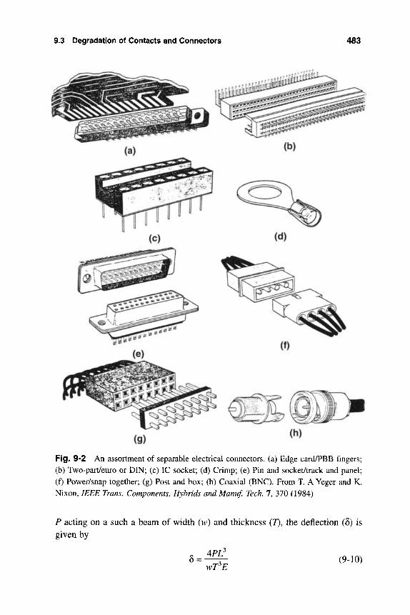
9.3 Degradation of Contacts and Connectors 483
Fig. 9-2 An assortment of separable electrical connectors, (a) Edge card/PBB fingers; (b) Two-part/euro or DIN; (c) IC socket; (d) Crimp; (e) Pin and socket/track and panel; (f) Power/snap together; (g) Post and box; (h) Coaxial (BNC). From T, A Yeger and K. Nixon, IEEE Trans. Components, Hybrids and Manuf. Tech 7, 370 (1984)
P acting on a such a beam of width (w) and thickness (J), the deflection (8) is
given by
4PL^ 6 =
wT^E (9-10)
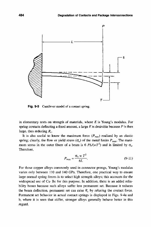
484 Degradation of Contacts and Package Interconnections
\—^
Fig. 9-3 Cantilever model of a contact spring.
in elementary texts on strength of materials, where E is Young's modulus. For spring contacts deflecting a fixed amount, a large E is desirable because P is then large, thus reducing R^,.
It is also useful to know the maximum force (Pmax) realized by an elastic spring; clearly, the flow or yield stress (GQ) of the metal limits Pmax- The maxi-mum stress in the outer fibers of a beam is 6 PL/(wT^) and is limited by Go-Therefore,
r2
6L (9-11)
For those copper alloys commonly used in connector prongs. Young's modulus varies only between 110 and 140 GPa. Therefore, one practical way to ensure large normal spring forces is to select high strength alloys; this accounts for the widespread use of Cu-Be for this purpose. In addition, there is an added relia-bility bonus because such alloys suffer less permanent set. Because it reduces the beam deflection, permanent set can raise Re by relaxing the contact force. Permanent set behavior in actual contact springs is displayed in Figs. 9-4a and b, where it is seen that stiffer, stronger alloys generally behave better in this regard.

0.010 r
-^ 0.008 c
C 72500 S
0.002 0.004 0.006 0.008 0.010 0.012 0.014 0.016
DEFLECTION (in.)
(a)
tu
H z lU z <
lii CL
0.001 f-
C 72500 S
C17200 C 51000 S
NUMBER OF CYCLES (b)
Fig. 9-4 (a) Pennanent set in three different copper base alloy spring connectors as a function of deflection. Note: C17200 is beryllium copper (E = 126GPa, Go = 721MPa), C51000 is phosphor bronze {E = 118GPa, G^ = 658MPa), C72500 is Gu-Ni-Sn {E = 134GPa, Go = 630MPa). (b) Permanent set in spring connectors as a function of the num-ber of contact mating cycles. From reference 6.
485
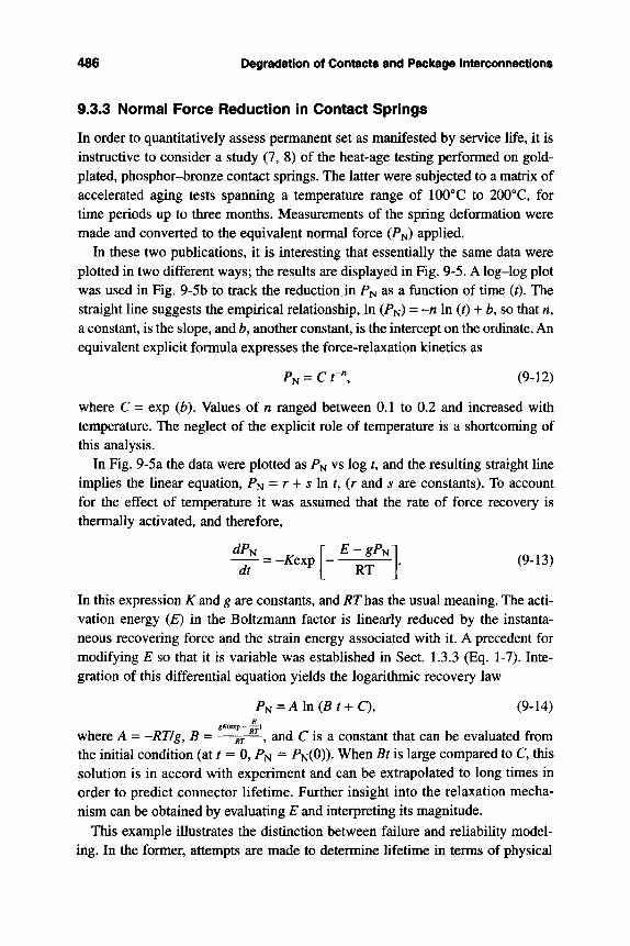
486 Degradation of Contacts and Package Interconnections
9.3.3 Normal Force Reduction in Contact Springs
In order to quantitatively assess permanent set as manifested by service life, it is instructive to consider a study (7, 8) of the heat-age testing performed on gold-plated, phosphor-bronze contact springs. The latter were subjected to a matrix of accelerated aging tests spanning a temperature range of 100°C to 200°C, for time periods up to three months. Measurements of the spring deformation were made and converted to the equivalent normal force (P^) applied.
In these two publications, it is interesting that essentially the same data were plotted in two different ways; the results are displayed in Fig. 9-5. A log-log plot was used in Fig. 9-5b to track the reduction in P^ as a function of time (t). The straight line suggests the empirical relationship. In (P f) = -n In (t) + b, so that n, a constant, is the slope, and b, another constant, is the intercept on the ordinate. An equivalent explicit formula expresses the force-relaxation kinetics as
/'N = C'r", (9-12)
where C = exp (b). Values of n ranged between 0.1 to 0.2 and increased with temperature. The neglect of the explicit role of temperature is a shortcoming of this analysis.
In Fig. 9-5a the data were plotted as PN VS log t, and the resulting straight line implies the linear equation, P^ = r -\- s In t, (r and s are constants). To account for the effect of temperature it was assumed that the rate of force recovery is thermally activated, and therefore.
dP^ —— = -^exp
dt E-gP^
RT (9-13)
In this expression K and g are constants, and RT has the usual meaning. The acti-vation energy (£) in the Boltzmann factor is linearly reduced by the instanta-neous recovering force and the strain energy associated with it. A precedent for modifying E so that it is variable was estabhshed in Sect. 1.3.3 (Eq. 1-7). Inte-gration of this differential equation yields the logarithmic recovery law
P^=Aln(Bt-\-Q, (9-14)
where A = -RT/g, B = — ^ — , and C is a constant that can be evaluated from the initial condition (at t = 0,P^ = P^(0)). When Bt is large compared to C, this solution is in accord with experiment and can be extrapolated to long times in order to predict connector lifetime. Further insight into the relaxation mecha-nism can be obtained by evaluating E and interpreting its magnitude.
This example illustrates the distinction between failure and reliability model-ing. In the former, attempts are made to determine lifetime in terms of physical
9.3 Degradation of Contacts and Connectors 487
Week Month
Time(f) (b)
10 Years
Fig. 9-5 (a) Force relaxation of a dual-cantilever electrical spring contact plotted as a function of log time. From reference 8. (b) Essentially the same data as in Fig. 9-5a plotted as log percent force reduction versus log time. From reference 7.
mechanisms that cause time-dependent changes in the material. Information pro-vided by the failure modeling leading to Eq. 9-14 often yields ideas for correc-tive action that may eventually eliminate the problem. On the other hand, no such information or hope stems from the empirical statistical modeling of relia-bility implicit in Eq. 9-12.
488 Degradation of Contacts and Package Interconnections
9.3.4 Tribology
The subject of tribology encompasses phenomena that occur at material surfaces in contact and in relative motion. These include wear, friction, erosion, and lubrication. Of these subjects, wear is clearly most important for our needs. In electronic packaging, wear scars develop in cable connectors and on the tab por-tions of card edge assemblies and pluggable modules. Specific mechanisms for damage have been reviewed by Engel (8) and include:
a. Adhesive wear Surface smearing, galling, and seizure are the manifestations of the adhesive wear that results from the microwelding of asperities. Such welds fracture in shear at the original interface or below it depending on the relative magnitude of the interfacial and cohesive bond strengths. When the adhesive strength exceeds the cohesive bond strength, wear particles may form after sev-eral cycles of contact. The wear volume (V) removed in this process is given by
K^PL y = - ^ . (9-15)
In this well-known expression due to Archard (10), P is the normal operative force, L is the length of relative surface displacement, H is the indentation hard-ness of the softer body, and AT is a dimensionless constant whose magnitude depends on the materials in contact. Typical values for K^ are 32 X 10-^ for Cu-Cu pairs, 12 x 10"^ for Ag-Ag pairs, and 1.5 for Cu on steel.
b. Abrasive wear In abrasive wear, hard surface asperities move against a softer material plowing it. Often particles enter the interface, and through cutting or grinding action the softer contact material is plowed or removed. The Archard expression describes the abrasive wear volume as well, but ATw may assume dif-ferent values depending on whether 2-body (contacting surfaces) or 3-body (contacting surfaces plus abrasive particles) are involved. Wear in this case depends strongly on the ratio /?w = abraded/ abrasive where H is hardness of the indicated material. For R^^ <\, extensive wear occurs, but when R^^ is slightly greater than unity, wear effectively ceases.
c. Delamination wear Due to the presence of cyclic loading, cracks can develop and propagate parallel to the surface. For sufficiently high tangential frictional stresses, thin platelike particles delaminate from the wearing surface.
d. Corrosive wear Continuous removal of surface films and chemical reac-tion between these wear products and the environment results in oxidation wear. Oxide films are generally brittle and protective when less than 10 |Lim thick. Under cyclic stressing the oxide may fracture, causing modest damage if the oxide particles are soft. Hard oxide particles, however, are abrasive and accel-erate wear.
9.3 Degradation of Contacts and Connectors 489
e. Fretting wear This important manifestation of contact wear is defined as accelerated surface damage occurring at the interface between contacting mate-rials subjected to small oscillatory movements. Fretting wear is often associated with adhesive, abrasive, and corrosive wear mechanisms. Because we are often concerned with the number of displacement cycles sustained prior to contact failure, low amplitude fatigue is one way to describe fretting.
9.3.5 Fretting Wear Phenomena
The micromotions that cause fretting in electronic connectors range from a few ILim to as much as 100 jim in length. They stem from mechanical vibrations, dif-ferential thermal expansion, and load relaxation of the contacting metals, as well as junction heating effects due to switching the power on and off. Manifestations of fretting damage include metal debris particles, wear scars, corrosion products, cracked surface oxide or sulfide films, and polymer formation from atmospheric organic precursors.
All metals (i.e., gold, palladium, tin, aluminum, nickel, silver, and copper) used for contacts and connectors suffer differing degrees of fretting damage depending on the particular metals involved, electrical power level, contact forces and frequency of loading, surface roughness, presence of lubricants, tem-perature, and environment. As Fig. 9-6a shows, fretting damage begins with cracking of surface films as a result of connector micromotions. Oxide regrows on the exposed metal but is in turn cracked with continued rubbing. Due to the accumulated damage during fretting, the contact resistance rises, as shown schematically in Fig. 9-6b. Following initial film cracking, a relatively long period of stable contact resistance ensues. Erratic resistance fluctuations are a precursor to the eventual failure, which is invariably manifested by a discontin-uous resistance rise and open contact.
Tests to evaluate fretting damage usually involve measurement of contact resistance changes under the wear track as a function of the number of loading (or displacement) cycles applied by mechanical, electromagnetic, or thermal means. Accelerated current cycling tests have also been performed. The results of extensive testing has yielded a reasonably coherent qualitative picture of the material behavior and wear phenomena observed. Some of this information (11-13) is summarized below:
1. Base metal (Sn, Sn-Pb solder) contacts oxidize rapidly and produce debris that accumulates in the contact zone.
2. Composition changes occur during fretting with dissimilar metals due to mass transfer, wear, and film formation. In general, the direction of metal transfer is from the softer to harder surface. Thus a Au-Pd contact maintains

BROKEN OXIDE FILM
"NEW" O X I D E - ^ i W ^ FILM ^ - - ^
I INITIAL
MICROMOTION
NEW" OXIDE FILM
7
MICROMOTION
AFTER N CYCLES,
INSULATED! (a)
100
Contact resistance (mil)
Drastic Increase
fretting tinne (cycles) (b)
Fig. 9-6 (a) Model of fretting corrosion damage in a contact undergo-ing micromotions. From reference 6. (b) Stages in the rise of contact resis-tance during fretting. From reference 14.
490
9.3 Degradation of Contacts and Connectors 491
low resistance because the harder palladium becomes coated with gold. Con-versely, Au-Sn contacts degrade as the softer tin coats the gold, effectively leaving a base metal contact behind. Intermetallic compound formation (e.g., Al-Cu) has been observed to occur at low temperatures.
3. Simultaneous corrosion virtually always accelerates fretting damage to con-tacts. The reduction in contact area causes either electrical or mechanical fail-ure or a combination of both effects. Through the use of noble metals, corro-sion effects are minimized. However, corrosion of the underlying base metal through pores in gold-plated contacts has been observed.
4. Metals such as Pd, Rh, and Ru catalyze the formation of frictional polymers from adsorbed organic air pollutants. Unlike fretting corrosion, the surfaces experience little or no wear.
5. Aluminum connectors in contact with Cu-Ni and Cu-Sn alloys are prone to wear by abrasion, adhesion, and delamination during fretting. Material trans-fer in both directions occurs.
6. Metals like Au, Ag, and Au-Pd-Ag alloys generally suffer little fretting dam-age and form little polymer.
7. Lubricants (contact aid compounds) can retard the rate of fretting and stabi-lize the contact resistance. Commercial lubricants are available to alleviate fretting problems by dispersing polymer buildup, reducing wear and shielding surfaces from oxidation. Paradoxically, lubricants do not have to be conduct-ing; their function is to protect the contact zone from the environment, not conduct electricity.
9.3.6 Modeling Fretting Corrosion Damage
In this section a portion of a recent quantitative model for fretting damage devel-oped by Bryant (14) is presented. The model assumes that the contact surface consists of a large number of hills and valleys. Initially clean asperities are exposed to corrosive attack, and films are formed. After fretting begins, valleys of the lower contact begin to fill with wear debris. Upon reversal of motion, these corrosion products are sheared off and fall into the valleys. When there is enough of an accumulation, the metal surfaces are separated by this nonconduc-tive debris, and the contact resistance rises until connector failure occurs.
To calculate a failure time, we assume that during the nth fretting cycle, a cor-rosive layer of thickness dc forms over the exposed valley area Agx, producing a volume of corrosion product Vc equal to dcA^^. The volume of reactant metal that generated Vc is equal to l/y, where y is the ratio of the volume of the corrosion compound to volume of metal. For copper, aluminum, and chromium, y > 1. Therefore, the asperity volume lost per cycle is Vasp = ^c ~ ^ = [^iK- When the
492 Degradation of Contacts and Package Interconnections
total asperity volume decrease is equal to a critical valley void volume y*, fail-ure occurs, or
A ,- Y - l N Y - l V* = Z - 4 7 - Vo(n) = X - h - dc Aex(n). (9-16)
n = 1 L y J n = 1 Y For average values over fretting cycles, this equation can be rearranged to yield the number of cycles (Nf) to failure
V*
y - i \ . , . (9-17)
In typical connectors, Af is predicted to range between 10^ to 10^ cycles. The normalized contact-resistance increase, as a function of corrosion debris volume, was theoretically shown to be constant until it reaches a value of 0.22 times the volume of the plastically deformed layer. A rapid resistance rise then signals fail-ure in a behavior that parallels that of Fig. 9-6b.
9.4 CREEP AND FATIGUE OF SOLDER
9.4.1 Introduction
Rather than have contacts that open and close, it is often necessary to have per-manent interconnections. As we have seen in Chapter 8, solders, perhaps the most ubiquitous of packaging materials, are almost universally employed for this purpose. While our previous concern was primarily with solder processing defects, we now focus on the reliability implications of soldered connections. For this purpose it is worthwhile reviewing Sect. 8.3, dealing with the metallur-gical change in phase microstructure and composition as well as intermetallic-compound growth in solders exposed to elevated temperatures. Troublesome thermal stresses, treated in Sect. 8-5, also arise to promote a variety of micro-scopic structural changes within the context of much broader macroscopic plastic-flow effects.
In practice, thermal cycling of electrical hardware generates corresponding stresses that couple both creep and fatigue effects to produce dynamic strains that often have important consequences for packaging reliability. The resulting deformation will generally vary in a complex way depending on the frequency and amplitude of the thermal stress cycle. Once creep and fatigue are individu-
9.4 Creep and Fatigue of Solder 493
ally well understood, thermal-cycling phenomena, which combine differing pro-portions of creep and fatigue deformation, will be more intelligible. That is why this section is primarily reserved for separate descriptions of creep and fatigue phenomena in solders.
In discussing stress relaxation and fretting damage in contacts, we have already treated manifestations of creep and fatigue previously in this chapter.
9.4.2 Creep—An Overview
When loads are applied to materials at elevated temperatures, they creep or plas-tically strain, provided that both the stresses and temperatures are sufficiently high. In crystalline solids, creep produces a number of irreversible deformation effects, e.g., dislocation migration, and annealing, viscous grain-boundary slid-ing, a reduction in residual stress, void formation, softening, and mechanical relaxation. Creep in metals and ceramics generally means stress levels near the yield point and temperatures of approximately 0.5 TM and above, where T^ is the melting point in degrees K. Electrical solder (60 Sn^OPb) melts at ~458K (185°C), and it is easy to appreciate its potential for creep even at room temper-ature, because 298K/458K = 0.65. Metal lead wires and tungsten filaments of incandescent bulbs operate at very high temperatures and are therefore strength-ened to resist creep. Ceramic substrates that typically melt above 2000°C will obviously not creep when used in electronic packaging. At the other extreme, polymers conamonly creep in a viscous fashion at low temperatures, i.e., between the glass transition and melting points. Even the tiny Si seed crystal that supports the hot, heavy single crystal being pulled during Czochralski growth does not appear to creep.
Creep is usefully viewed as an admixture of two simultaneous effects; one is strain hardening, and the other is softening due to recrystallization and aging effects. Three regimes of creep deformation can be distinguished, depending on the magnitudes of the hardening and softening rates. When a tensile or shear load is applied under creep conditions, the material instantaneously stretches or strains the predictable elastic amount, after which the strain increases with time at an ever decreasing rate. In the primary creep stage the hardening rate exceeds that for softening. This primary-deformation stage then gives way imperceptibly to a regime of steady-state, or secondary, creep, where the hardening rate is bal-anced by the softening rate. As a result, the overall creep strain rate (de/dt) is constant. Design of operating conditions for creep-prone components is usually performed in this regime because time-dependent deformation can be confi-dently projected into the future. Steady-state creep phenomena also pose relia-bility concerns because potentially large plastic strains can develop. Finally, in
494 Degradation of Contacts and Package Interconnections
the tertiary creep stage the strain increases rapidly with time, leading to failures characterized by much stretching and thinning, void cavitation at grain bound-aries, and intergranular cracking. In our subsequent discussion of solder creep we will be exclusively concerned with these last two deformation regimes.
9.4.3 Constitutive Equations of Creep
In the broadest sense, the creep strain (e) that develops is a function of time (0 as well as applied stress (a) and temperature (7). Often, shear stresses (x) and strains (y) are involved, and we shall simply represent these by the generic a and € for simplicity. Furthermore, e is assumed to be a product of three separate fac-tors, one of which is the ubiquitous Boltzmann factor; therefore, the constitutive equations for the creep strain and strain rates assume the respective forms
€ =y(a) g(t) exp RT
and
^ = e = / ( a ) -dgify
dt exp
RT _
(9-18a)
(9-18b)
Explicit expressions for the / (a) and g(t) factors, and the researchers associ-ated with them, are (15)
f(c) = Acf Norton g(t) = (1 + et^^^) Andrade (primary creep)
= Bsinh(ba) Prandtl = t Steady-state (secondary creep)
C exp (c a) Dom = t" Bailey (tertiary creep)
= D s i n h ( / a ) " Garafalo,
where A, B, C, D, b, c, e, f, n, and m are constants, E^ is the creep activation energy, and RT has the usual meaning. For crystalline solids, E^ is close in mag-nitude to a diffusional activation energy because creep cannot occur without simultaneous atomic motion. Depending on whether deformation primarily occurs within grains or at grain boundaries, activation energies applicable to these mechanisms would be appropriate. As we shall see, the stress exponent n typically ranges from 1 to 8, depending on the material, stress/temperature range, and creep mechanism.
In each creep regime an equation for both e and dddt can now be constructed by selecting the appropriate forms of (a) and g{t). For short deformation times
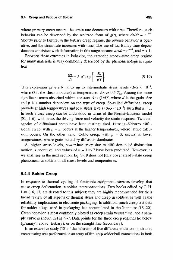
9.4 Creep and Fatigue of Solder 495
where primary creep occurs, the strain rate decreases with time. Therefore, such behavior can be described by the Andrade form of g(t), where de/dt ~ r^^^. Shortly prior to failure, in the tertiary creep regime, the reverse behavior is oper-ative, and the strain rate increases with time. The use of the Bailey time depen-dence is consistent with deformation in this range because de/dt ~ /'"~\ and m > 1.
Between these extremes in behavior, the extended steady-state creep regime for many materials is very commonly described by the phenomenological equa-tion
—- = A a"exp dt RT
(9-19)
This expression generally holds up to intermediate stress levels {olG < 10"^, where G is the shear modulus) at temperatures above 0.5 Ty^. Among the more significant terms absorbed within constant A is {\ldf, where d is the grain size and / is a number dependent on the type of creep. So-called diffusional creep prevails at high temperatures and low stress levels {alG < 10"^) such that n= \. In such a case creep can be understood in terms of the Nemst-Einstein model (Eq. 1-6), with stress the driving force and velocity the strain response. Two cat-egories of diffusional creep have been distinguished. Herring-Nabarro diffu-sional creep, with p = 2, occurs at the higher temperatures, where lattice diffu-sion occurs. On the other hand, Coble creep, with p = 3, occurs at lower temperatures, where grain-boundary diffusion dominates.
At higher stress levels, power-law creep due to diffusion-aided dislocation motion is operative, and values of fi = 3 to 7 have been predicted. However, as we shall see in the next section, Eq. 9-19 does not fully cover steady-state creep phenomena in solders at all stress levels and temperatures.
9.4.4 Solder Creep
In response to thermal cycling of electronic equipment, stresses develop that cause creep deformation in solder interconnections. Two books edited by J. H. Lau (16, 17) are devoted to this subject; they are highly recommended for their broad review of all aspects of thermal stress and creep in solders, as well as the reliability implications in electronic packaging. In addition, much creep test data for solder alloys used in packaging has accumulated in the literature (18-20). Creep behavior is most conmionly plotted as creep strain versus time, and a sam-ple curve is shown in Fig. 9-7. Data points for the three creep regimes lie below (primary), above (tertiary), or on the straight line (secondary).
In an extensive study (18) of the behavior of five different solder compositions, creep testing was performed on an array of flip-chip solder ball connections in both
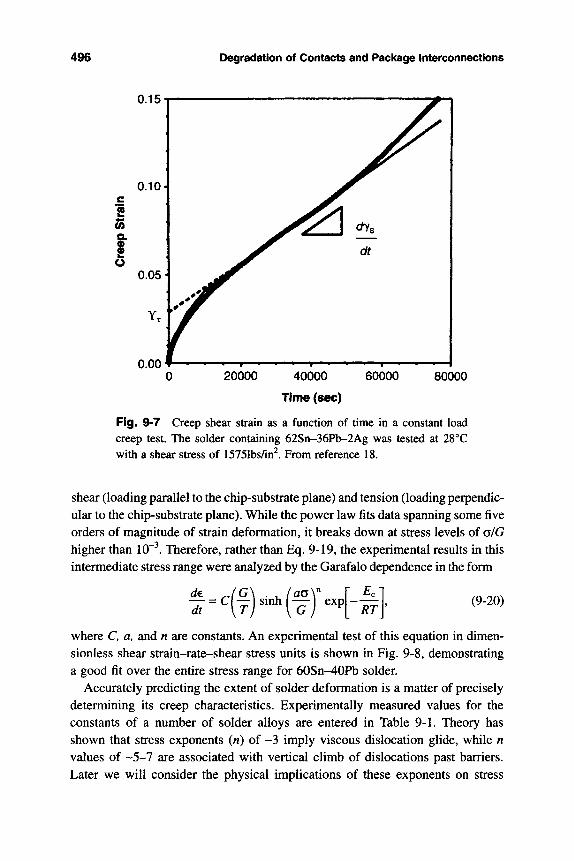
496 Degradation of Contacts and Package Interconnections
0.15
0.10
in Q.
o
0.00 20000 40000
Time (sec)
60000 80000
Fig. 9-7 Creep shear strain as a function of time in a constant load creep test. The solder containing 62Sn-36Pb-2Ag was tested at 28°C with a shear stress of 15751bs/in . From reference 18.
shear (loading parallel to the chip-substrate plane) and tension (loading perpendic-ular to the chip-substrate plane). While the power law fits data spanning some five orders of magnitude of strain deformation, it breaks down at stress levels of (5lG higher than 10"^. Therefore, rather than Eq. 9-19, the experimental results in this intermediate stress range were analyzed by the Garafalo dependence in the form
f = c ( f ) s i n h ( f . exp . - ^^ (9-20)
where C, a, and n are constants. An experimental test of this equation in dimen-sionless shear strain-rate-shear stress units is shown in Fig. 9-8, demonstrating a good fit over the entire stress range for 60Sn^0Pb solder.
Accurately predicting the extent of solder deformation is a matter of precisely determining its creep characteristics. Experimentally measured values for the constants of a number of solder alloys are entered in Table 9-1. Theory has shown that stress exponents (w) of -3 imply viscous dislocation glide, while n values of ~5-7 are associated with vertical climb of dislocations past barriers. Later we will consider the physical implications of these exponents on stress
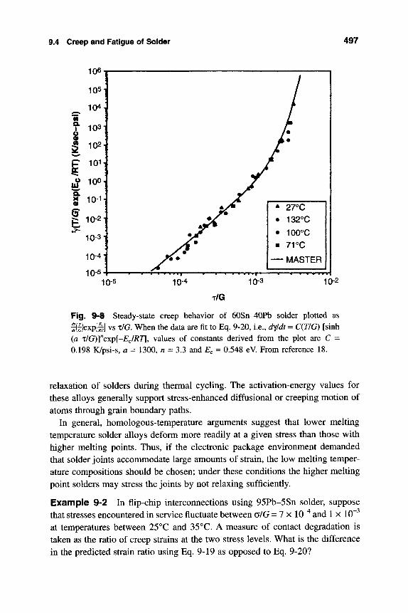
9.4 Creep and Fatigue of Solder 497
lU"]
105]
^ 10^1 • «
1 10^1 ^ i ^
P 1011 C !
^ ^^^1 ^ . " X 10-11
^ 10-21 <^«e
10-3]
10-4]
10-5 -
1 ^ ^ \
£ 1
-^ 1
A V "
. ^ • X
4^^ • > •
>* *
^ 27°G 1 • 132°C
• 100°C
• 7rc — MASTER
» 1 • 1 > 1 1 1 1
10-5 tO-4 10-3 10-2
T / G
Fig. 9-8 Steady-state creep behavior of 60Sn-40R) solder plotted as f(f)exp[|;] vs T/G. When the data are fit to Eq. 9-20, i.e., didt = C{TIG) [sinh {a XIG)TQX^[-EJRT\, values of constants derived from the plot are C = 0.198 K/psi-s, a = 1300, n = 3.3 and E = 0.548 eV. From reference 18.
relaxation of solders during thermal cycling. The activation-energy values for these alloys generally support stress-enhanced diffusional or creeping motion of atoms through grain boundary paths.
In general, homologous-temperature arguments suggest that lower melting temperature solder alloys deform more readily at a given stress than those with higher melting points. Thus, if the electronic package environment demanded that solder joints accommodate large amounts of strain, the low melting temper-ature compositions should be chosen; under ttiese conditions the higher melting point solders may stress the joints by not relaxing sufficiently.
Example 9-2 In flip-chip interconnections using 95Pb-5Sn solder, suppose that stresses encountered in service fluctuate between olG = 7 x 10"^ and 1 x 10"^ at temperatures between 25°C and 35°C. A measure of contact degradation is taken as the ratio of creep strains at the two stress levels. What is the difference in the predicted strain ratio using Eq. 9-19 as opposed to Eq. 9-20?
498 Degradation of Contacts and Package Interconnections
Table 9-1 Creep Constants for Solder Alloys
Composition
96.5Sn-3.5Ag 62Sn-36Pb-2Ag 60Sn-40Pb 97Pb-3Sn 95Pb-5Sn 96.5Sn-3.5Ag
C (K/psi-s)
4.89 X 10"^ 98.9 X 10"^ 198 X 10"^ 5.04 X 10^ 1.21 X 10^ 3.13 X 10"^
a
1300 1300 1300 1200 1000 1500
n
5.5 3.3 3.3 7.0 7.0 5.5
£c (kcal/mol)
9.2 12.6 12.6 27.7 27.7 11.5
From references 17, 18, and 19.
Answer We refer to the high stress/temperature state as 2 and the low stress/temperature state as 1. In the case of Eq. 9-19, noting that n = 7.0 and £c = 27.7 kcal /mol,
€2 \(5^QX^[-EJRT2] (1 X 10"')^ exp[-27J00/(1.99 (308))]
ei " A (5lQx^[-EJRTy] ~ (7 x lO" )" exp[-27,700/(1.99 (298))]
In contrast, the use of Eq. 9-20 where a = 1000 and n = 7.0, yields
€2 (298) (sinh 1) exp[-27,700/(1.99 (308))]
= 55.3.
(308) (sinh 0.7)^ exp[-27,700/(1.99 (298))] = 9.4.
Therefore, depending on which constitutive equation is chosen, a difference by a factor of 5.9 can result in estimating strain acceleration.
9.4,5 Fatigue—An Overview
Failures due to fatigue are the most common and insidious that metals suffer from. After propagating for some time, unnoticed cracks suddenly and without warning cause fracture of components. Although fatigue is popularly associated with the failure of highly-stressed rotating machinery, it also occurs in electrical equipment in the form of damage to moving contacts as well as vibrating and thermally cycled components. The cyclic loading can be sinusoidal about a mean zero stress level, but any other high- or low-frequency quasi-periodic stress dis-tribution can also cause fatigue failure. Some materials, like steel, display an endurance limit, a critical stress level below which failure does not occur irre-spective of the number of cycles; aluminum and polymers show no such endurance limit. These as well as other fatigue phenomena are reviewed in stan-dard texts on the mechanical properties of materials (21).
A microscopic model for fatigue damage in crystalline materials starts with cyclic dislocation displacements on slip planes in concert with the applied load.
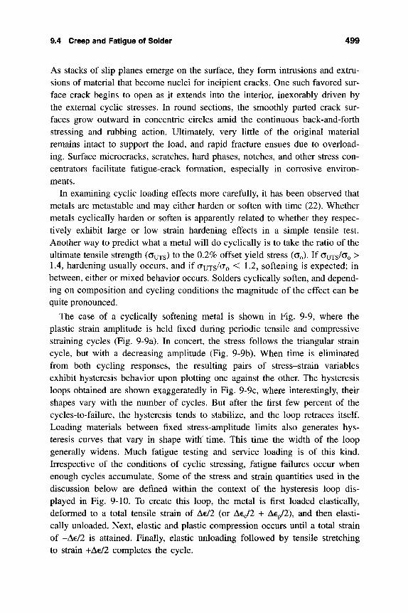
9.4 Creep and Fatigue of Solder 499
As stacks of slip planes emerge on the surface, they form intrusions and extru-sions of material that become nuclei for incipient cracks. One such favored sur-face crack begins to open as it extends into the interior, inexorably driven by the external cyclic stresses. In round sections, the smoothly parted crack sur-faces grow outward in concentric circles amid the continuous back-and-forth stressing and rubbing action. Ultimately, very little of the original material remains intact to support the load, and rapid fracture ensues due to overload-ing. Surface microcracks, scratches, hard phases, notches, and other stress con-centrators facilitate fatigue-crack formation, especially in corrosive environ-ments.
In examining cyclic loading effects more carefully, it has been observed that metals are metastable and may either harden or soften with time (22). Whether metals cyclically harden or soften is apparently related to whether they respec-tively exhibit large or low strain hardening effects in a simple tensile test. Another way to predict what a metal will do cyclically is to take the ratio of the ultimate tensile strength (GUTS) to the 0.2% offset yield stress (Go). If GUTS/<^O > 1.4, hardening usually occurs, and if auis/^o ^ 1 -2, softening is expected; in between, either or mixed behavior occurs. Solders cyclically soften, and depend-ing on composition and cycling conditions the magnitude of the effect can be quite pronounced.
The case of a cyclically softening metal is shown in Fig. 9-9, where the plastic strain amplitude is held fixed during periodic tensile and compressive straining cycles (Fig. 9-9a). In concert, the stress follows the triangular strain cycle, but with a decreasing amplitude (Fig. 9-9b). When time is eliminated from both cycling responses, the resulting pairs of stress-strain variables exhibit hysteresis behavior upon plotting one against the other. The hysteresis loops obtained are shown exaggeratedly in Fig. 9-9c, where interestingly, their shapes vary with the number of cycles. But after the first few percent of the cycles-to-failure, the hysteresis tends to stabilize, and the loop retraces itself. Loading materials between fixed stress-amplitude limits also generates hys-teresis curves that vary in shape witlf time. This time the width of the loop generally widens. Much fatigue testing and service loading is of this kind. Irrespective of the conditions of cyclic stressing, fatigue failures occur when enough cycles accumulate. Some of the stress and strain quantities used in the discussion below are defined within the context of the hysteresis loop dis-played in Fig. 9-10. To create this loop, the metal is first loaded elastically, deformed to a total tensile strain of Ae/2 (or Aejl + A€p/2), and then elasti-cally unloaded. Next, elastic and plastic compression occurs until a total strain of -Ae/2 is attained. Finally, elastic unloading followed by tensile stretching to strain -l-Ae/2 completes the cycle.
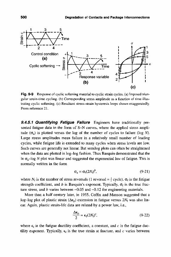
500 Degradation of Contacts and Package Interconnections
c
CO
i+f
Time
2 4
Control condition (a)
+K
Cyclic softening—• % CO
Time
Response variable
(b)
a 1 • ^r-Tjl
4 J H - ^ ^X
J>i^ i-* ihb
1
(c)
Fig. 9-9 Response of cyclic softening material to cyclic strain cycles, (a) Imposed trian-gular strain-time cycling, (b) Corresponding stress amplitude as a function of time illus-trating cyclic softening, (c) Resultant stress-strain hysteresis loops shown exaggeratedly. From reference 21.
9.4.5.1 Quantifying Fatigue Faiiure Engineers have traditionally pre-sented fatigue data in the form of S-N curves, where the applied stress ampli-tude (Ga) is plotted versus the log of the number of cycles to failure (log AO-Large stress amplitudes mean failure in a relatively small number of loading cycles, while fatigue life is extended to many cycles when stress levels are low. Such curves are generally not linear. But semilog plots can often be straightened when the data are plotted in log-log fashion. Thus Basquin demonstrated that the In (Ta-log A plot was linear and suggested the exponential law of fatigue. This is normally written in the form
^ Of(2Nf)\ (9-21)
where Nf is the number of stress reversals (1 reversal = \ cycle), Gf is the fatigue strength coefficient, and b is Basquin's exponent. Typically, Gf is the true frac-ture stress, and b varies between -0.05 and -0.12 for engineering materials.
More than a half century later, in 1955, Coffin and Manson suggested that a log-log plot of plastic strain (ACp) extension in fatigue versus 2Nf was also lin-ear. Again, plastic strain-life data are related by a power law, i.e..
A€„ = €f(2A^f)^ (9-22)
where €f is the fatigue ductility coefficient, a constant, and c is the fatigue duc-tility exponent. Typically, €f is the true strain at fracture, and c varies between
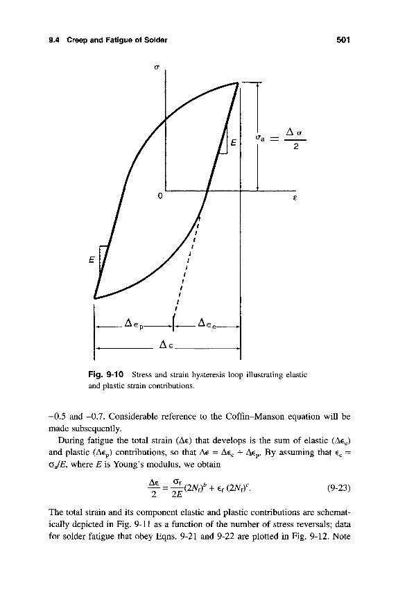
9.4 Creep and Fatigue of Solder 501
Fig. 9-10 Stress and strain hysteresis loop illustrating elastic and plastic strain contributions.
-0.5 and -0.7. Considerable reference to the Coffin-Manson equation will be made subsequently.
During fatigue the total strain (Ae) that develops is the sum of elastic (Ace) and plastic (Acp) contributions, so that Ae = Acg + Acp. By assuming that Eg = GJE, where E is Young's modulus, we obtain
~- = ^{2N,f^e,{2N,r. (9-23)
The total strain and its component elastic and plastic contributions are schemat-ically depicted in Fig. 9-11 as a function of the number of stress reversals; data for solder fatigue that obey Eqns. 9-21 and 9-22 are plotted in Fig. 9-12. Note
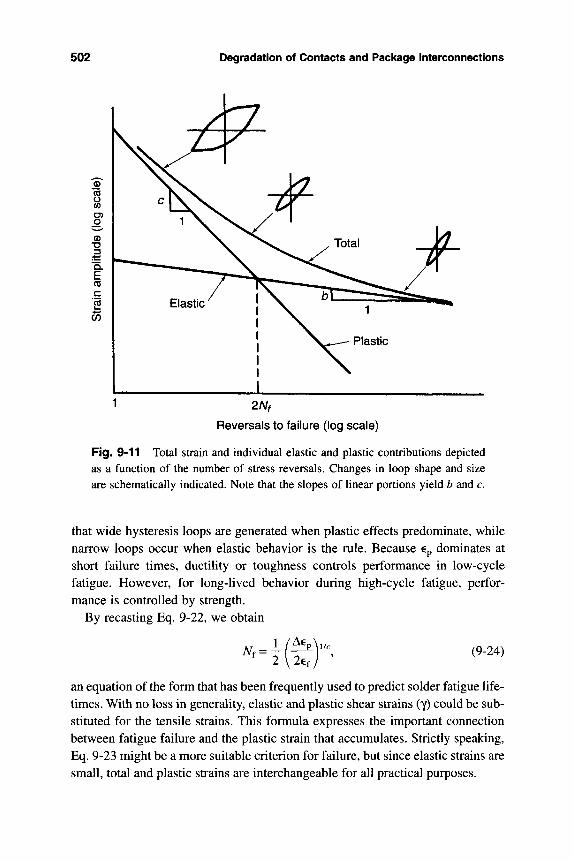
502 Degradation of Contacts and Package Interconnections
Reversals to failure (log scale)
Fig. 9-11 Total strain and individual elastic and plastic contributions depicted as a function of the number of stress reversals. Changes in loop shape and size are schematically indicated. Note that the slopes of linear portions yield b and c.
that wide hysteresis loops are generated when plastic effects predominate, while narrow loops occur when elastic behavior is the rule. Because €p dominates at short failure times, ductility or toughness controls performance in low-cycle fatigue. However, for long-lived behavior during high-cycle fatigue, perfor-mance is controlled by strength.
By recasting Eq. 9-22, we obtain
'4(t"" (9-24)
an equation of the form that has been frequently used to predict solder fatigue life-times. With no loss in generality, elastic and plastic shear strains (y) could be sub-stituted for the tensile strains. This formula expresses the important connection between fatigue failure and the plastic strain that accumulates. Strictly speaking, Eq. 9-23 might be a more suitable criterion for failure, but since elastic strains are small, total and plastic strains are interchangeable for all practical purposes.
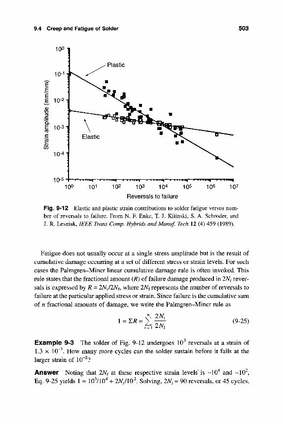
9.4 Creep and Fatigue of Solder 503
100 1
Plastic
100 101 102 103 104 105 106 107
Reversals to failure
Fig. 9-12 Elastic and plastic strain contributions to solder fatigue versus num-ber of reversals to failure. From N. F. Enke, T. J. Kilinski, S. A. Schroder, and J. R. Lesniak, IEEE Trans Comp. Hybrids and Manuf. Tech 12 (4) 459 (1989).
Fatigue does not usually occur at a single stress amplitude but is the result of cumulative damage occurring at a set of different stress or strain levels. For such cases the Palmgren-Miner linear cumulative damage rule is often invoked. This rule states that the fractional amount (R) of failure damage produced in 2Ni rever-sals is expressed by R = IN-JlNf, where INf represents the number of reversals to failure at the particular applied stress or strain. Since failure is the cumulative sum of n fractional amounts of damage, we write the Palmgren-Miner rule as
1 E/? = y —- (9-25)
Example 9-3 The solder of Fig. 9-12 undergoes 10^ reversals at a strain of 1.3 X 10"^. How many more cycles can the solder sustain before it fails at the larger strain of 10"^?
Answer Noting that 2Nf at these respective strain levels is -10"^ and -10^, Eq. 9-25 yields 1 = 10^/10^ -h INi/lO^. Solving, 2Ni = 90 reversals, or 45 cycles.
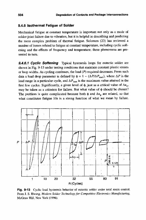
504 Degradation of Contacts and Package Interconnections
9.4.6 isothermal Fatigue of Soider
Mechanical fatigue at constant temperature is important not only as a mode of solder-joint failure due to vibration, but it is helpful in describing and predicting the more complex problem of thermal fatigue. Solomon (23) has reviewed a number of issues related to fatigue at constant temperature, including cyclic soft-ening and the effects of frequency and temperature; these phenomena are pre-sented in turn.
9.4,6.1 Cyclic Softening Typical hysteresis loops for eutectic solder are shown in Fig. 9-13 under testing conditions that maintain constant plastic strains or loop widths. As cycHng continues, the load (P) required decreases. From such data a load drop parameter is defined by (j) = 1 - (AP/APmax)» where AP is the load range in a particular cycle, and AP^ax is the maximum value attained in the first few cycles. Significantly, a given level of (|), just as a critical value of ACp, may be taken as a criterion for failure. But what value of ^ should be chosen? The problem is quite complicated because both (|) and Acp are related, so that what constitutes fatigue life is a strong function of what we mean by failure.
[*A7--|
r
cvj 0.123
32
A/(Cycles)
55 80 91
Fig. 9-13 Cyclic load hysteresis behavior of eutectic solder under total strain control. From J. S. Hwang, Modem Solder Technology for Competitive Electronics Manufacturing, McGraw Hill, New York (1996).
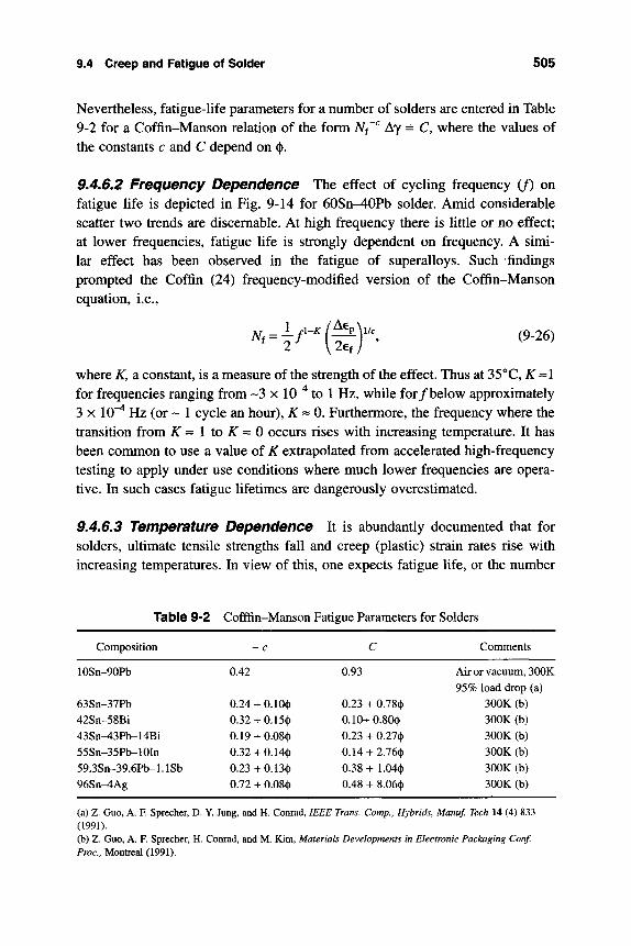
9.4 Creep and Fatigue of Solder 505
Nevertheless, fatigue-life parameters for a number of solders are entered in Table 9-2 for a Coffin-Manson relation of the form Nf^ Ay = C, where the values of the constants c and C depend on (|).
9.4,6,2 Frequency Dependence The effect of cycling frequency (J) on fatigue life is depicted in Fig. 9-14 for 6GSn^0Pb solder. Amid considerable scatter two trends are discemable. At high frequency there is little or no effect; at lower frequencies, fatigue life is strongly dependent on frequency. A simi-lar effect has been observed in the fatigue of superalloys. Such findings prompted the Coffin (24) frequency-modified version of the Coffin-Manson equation, i.e.,
-.4/"(t P \l/c (9-26)
where Ky a constant, is a measure of the strength of the effect. Thus at 35°C, K-l for frequencies ranging from ~3 x 10"^ to 1 Hz, while for/below approximately 3 X 10"^ Hz (or ~ 1 cycle an hour), i^ ~ 0. Furthermore, the frequency where the transition from ^ = 1 to ^ = 0 occurs rises with increasing temperature. It has been conmion to use a value of K extrapolated from accelerated high-frequency testing to apply under use conditions where much lower frequencies are opera-tive. In such cases fatigue lifetimes are dangerously overestimated.
9,4,6,3 Temperature Dependence It is abundantly documented that for solders, ultimate tensile strengths fall and creep (plastic) strain rates rise with increasing temperatures. In view of this, one expects fatigue life, or the number
Table 9-2 Cofffin-Manson Fatigue Parameters for Solders
Composition Comments
10Sn-90Pb
63Sn-37Pb 42Sn-58Bi 43Sn-43Pb-14Bi 55Sn-35Pb-10In 59.3Sn-39.6Pb-LlSb 96Sn-4Ag
0.42
0.24 + 0.10(1) 0.32 + 0.15(1) 0.19 + 0.08(1) 0.32 + 0.14(|) 0.23 + 0.13(1) 0.72 + 0.08(1)
0.93
0.23 + 0.78(|) 0.10+0.80(1) 0.23 + 0.27(1) 0.14 + 2.76(1) 0.38 + 1.04(|) 0.48 + 8.06(1)
Air or vacuum, 300K 95% load drop (a)
300K (b) 300K(b) 300K (b) 300K (b) 300K (b) 300K (b)
(a) Z. Guo, A. F. Sprecher, D. Y. Jung, and H. Conrad, IEEE Trans. Comp., Hybrids, Manuf. Tech 14 (4) 833 (1991). (b) Z. Guo, A. F, Sprecher, H. Conrad, and M. Kim, Materials Developments in Electronic Packaging Conf. Proc, Montreal (1991).
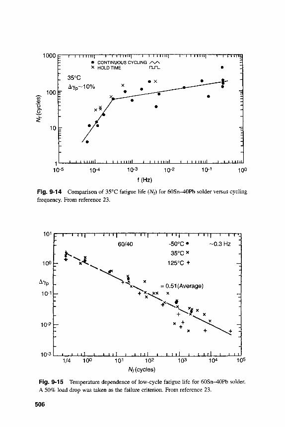
1000
loot" 0)
o o
P" r
P L
L-
P
L
r
-1—TT
35°C
A7p-
- J L-l
1 I I IH 1—TTTTTII] - I I I M I I I | 1 • CONTINUOUS CYCLING / \ ^ X HOLD TIME
'10% ^ •
xy
• / •
/ #
u i i i L . . . 1 1 1 i i i i i l
R-TL
• X
• . "S"
•
i 1 I I Hi l l
... 1 J ,1 , , , l - -
•
•
1 I I m i l ..
r~T-r
•
•
J _.,LJ
TTTm
3 H
-|
-J
1
-J
H
1 1 iml
1 0 k
r 10-5 10-4 10-3 10-2 10-'' 100
f(Hz)
Fig. 9-14 Comparison of 35°C fatigue life (A f) for 60Sn^0Pb solder versus cycling frequency. From reference 23.
p — T — r n r n — ' — r r r ] — i — r r r i — i — r r v ] — i — T - T T J — i — n r r
60/40 -50°C« -0.3 Hz
35X ^
125°C +
= 0.51 (Average)
101
100
10-1
10-2
10-3 1 1 . 1 I I I I I M I t J j - I 1 tl t i l l \ i 1 I 1/4 100 101 102
A/ (cycles)
103 104 105
Fig. 9-15 Temperature dependence of low-cycle fatigue life for 60Sn-40Pb solder. A 50% load drop was taken as the failure criterion. From reference 23.
506
9.5 Reliability and Failure of Solder Joints 507
of cycles to failure, to be strongly temperature dependent. Confounding intu-ition, while there is a temperature dependence, it is not a large one nor, consid-ering the statistical uncertainties in the data for 60Sn-40Pb solder shown in Fig. 9-15, a particularly significant one (23). The same is true of the high-lead sol-ders. Solomon has suggested that claims for larger reported temperature depen-dencies in high-lead-tin solders may be exaggerated due to scatter in the data.
9.5 RELIABILITY AND FAILURE OF SOLDER JOINTS
9.5.1 Introduction to Thermal Cycling Effects
The previous sections dealing with creep and fatigue assumed that 1. isolated (unattached) solder materials were involved, and 2. deformation occurred under isothermal conditions. Now we address the more complicated issues associated with thermally cycled solder joints attached to IC chips, packages and circuit boards. The objective is to understand the processes that lead to mechanical failure. We recall that the thermal stresses in solders (adhesives) that we calcu-lated at great length in Chapter 8 were elastic shear stresses. However, in this chapter we have already noted that accumulated plastic strain is what causes failure of solder during creep or fatigue. How are elastic shear stresses, which after all produce small elastic strains, related to the much larger plastic strains? In addressing this question and others related to thermal cycling of solder joints, a review of thermal expansion mismatch effects is a good place to begin.
9.5.1.1 Thermal Cycling Distortion of Solder Joints Following Solomon (23), consider a chip or component (c) attached to printed wiring board (PWB) substrate (s) by means of a solder post of height h, all at temperature T^. The thermal expansion coefficients a(c) and a(s) are such that a(s) > a(c) for the geometry shown in Fig. 9-16a. We note that heating and cooling essentially fatigues the solder joints through the shear strain reversals depicted in Figs. 9-16b and 9-16c, respectively. It is not hard to calculate the strain that develops. First, taking the difference in the expanded lengths on heating to T^AX yields the net displacement of both joints as L [a(s) - a(c)](rMAx - ^o)- Similarly, during cooling to TMIN, the net displacement of both joints is L [a(s) - oc(c)](rMiN ~ ^o)-The net total thermal displacement (A) after heating followed by cooling is the difference in these, or A = L [a(s) - a(c)](rMAx - ^MIN)- By definition, the shear strain (y) per joint is y = A/(2/z), so that
IE. cc
PWB
(a)
-H- Solder
Lc=/-[1+a(c)(TMAX-To)],
CC
zz x . Ls=/.[1+a(s)(rMAX-7-o)]
(b)
r H
cc VY ZZ
h Ls=L[1+a(s)(rM,N-To]
(c) Fig. 9-16 Assorted thermal effects in soldered joint connecting a chip car-rier (CC) to a substrate (PWB). Assembly at temperature To with thermal expansion coefficients a(c) and a(s), such that a(s) > a(c). (a) Initially unstressed solder joint, (b) Solder joint is heated to T^AX, expanding PWB rel-ative to CC. (c) Solder joint is cooled to T^IN, contracting PWB relative to CC. From reference 23.
508
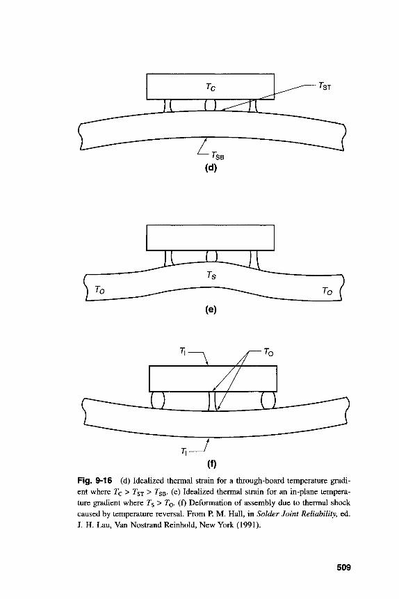
Fig. 9-16 (d) Idealized thermal strain for a through-board temperature gradi-ent where Tc> TsT > TsB' (e) Idealized thermal strain for an in-plane tempera-ture gradient where Ts > TQ. (f) Deformation of assembly due to thermal shock caused by temperature reversal. From P. M. Hall, in Solder Joint Reliability, ed. J. H. Lau, Van Nostrand Reinhold, New York (1991).
509
510 Degradation of Contacts and Package Interconnections
Y = 1-^] [a(s) - a(c)](r^^x - T^^^l (9-27)
9.5.1.2 Conversion of Elastic Strain to Plastic Strain It might be imagined that thermal flexing of the assembly in Fig. 9-16 would yield the same bend angles (positive and negative) for identical temperature excursions above and below the ambient (stress-free) temperature datum. This, after all, is how bimetallic strips respond to temperature. But as seen in Fig. 9-17, this does not happen. Instead of reversible elastic bending, an asymmetrically shaped hystere-sis loop develops, indicating that the thermal behavior of the solder is influenc-ing the overall response of the assembly.
This behavior is related to the question raised at the beginning of this section, which is now addressed. First we note that solder joints are elastically strained as well as stressed during thermal cycling. With time at elevated temperature, however, the elastic strain is essentially converted into plastic strain. This effec-
Bimetallic Strip Theory
J I I I I I I 0 20 40 60 80 100 120 140
Temperature (°C)
Fig. 9-17 Bend angles as a function of temperature in a soldered plate assembly sub-jected to reversed bending. Deviation from bimetallic strip theory is indicated. Hysteresis in bend angles (positive and negative) occurs due to temperature excursions above and below the ambient temperature (stress-free) datum. From P. M. Hall, IEEE Comp. Hybrids and Manuf. Tech. 1 (4) 314 (1984).
9.5 Reliability and Failure of Solder Joints 511
lively limits the bend angle at elevated temperatures. To see why, we model the viscoelastic solder by a spring (of constant k^) displaying elastic behavior, and by a dashpot (of viscosity r|) that embodies its viscous nature. Solder behaves viscously during creep when dislocations and vacancies move or grain bound-aries slide. In the classic Maxwell model of a viscoelastic solid (24) consisting of a spring and dashpot in series, consider what happens when this combination is stretched to a total strain (e^) that remains fixed thereafter. This is like the problem of a bolt initially tightened by force P^ to a high stress level (Go) that then relaxes with time through viscous flow. The subsequent force (stress) relax-ation behavior as a function of time (t) is described by
, or a (0 = Go exp Pit) = Po exp r\
(9-28)
where the decay time constant t^ is related to the ratio of Young's modulus to the effective viscosity. Again, with no loss in generality, shear stresses (x) can be substituted for tensile stresses in Eq. 9-28. Since the elastic strain (Cg) is G (t)/E, and €o = Cg + Cp, the plastic strain (Cp) is given by
f)»p(-i). (9-29,
Thus, with time the elastic strain is irreversibly diminished and replaced by plastic strain. It is this accumulated plastic strain that eventually causes fatigue failure when it reaches a critical level.
9-5-7.3 Thermal Distortion of Nonuniformiy Heated Solder Joints In the cases of solder-joint distortion just treated, the chip, solder, and substrate were all assumed to be at the same temperature whether it was T^^x, r iN, or T^. But other scenarios for circuit-board distortion occur in practice. For example, in Fig. 9-16d the chip carrier dissipates heat, so that there is a thermal gradient in the vertical direction. As a result of the hot spot, the top of the PWB is hotter (JST) than the bottom (TSB), causing it to bow downward as shown. In addition to through-board gradients there may be in-plane thermal gradients generated by neighboring components. This causes similar convex bowing that buckles the PWB in the manner shown in Fig. 9-16e. In both of these cases it is assumed that the solder is totally relaxed, so that the outer solder posts are extended while the inner one is compressed.
Another environment of interest in packaging is thermal shock. Here the tem-perature is changed so rapidly that the inner parts (TQ) thermally lag the response of the outer parts (Ti). Therefore, by inverting the temperature distribution, the resulting distortion in Fig. 9-16f is reversed.
512 Degradation of Contacts and Package Interconnections
9.5.2 Thermal-Stress Cycling of Surface-Mount Solder Joints
9.5.2.1 Scope We now treat the case of thermal fatigue that occurs during thermal cycling of surface-mounted packages. Merely turning electrical equip-ment on and off is the simplest way to generate such periodic thermal stressing. The isothermal loading cycle that was considered in Sect. 9.4.6 is clearly a sim-pler process than the case now being addressed. Engelmaier and coworkers (26-28) have extensively studied the problem of thermal fatigue in surface-mount (SM) solder joints and the related issue of design for long-term reliabil-ity. Two types of SM joints were considered—leadless and leaded (see Fig. 8-18). Leadless joints are stiff and sustain high stress levels, but occupy little space on the board. On the other hand, leaded joints are compliant, enabling them to reduce stress levels below the solder yield stress, thus minimizing cyclic fatigue damage as a result. The lower stress levels, in turn, slow and may even arrest harmful viscoplastic stress-relaxation and creep processes. As a result, leaded joints suffer lead fracture, while solder fatigue is the usual failure mechanism in leadless joints. The difference in these two joints is reflected in their response to thermal cycling, as indicated in the hysteresis loops of Fig. 9-18a and b. Simu-lated hysteresis loops for a number of different thermally cycled solders are plot-ted in Fig. 9-19 and reveal similar behavior.
9.5.2.2 Leadless Joints In the case of the leadless surface-mount solder joint at high temperature, elastic-plastic, shear stress-strain deformation occurs. Beyond the initial elastic response in Fig. 9-16a, the solder essentially yields at a constant stress level (XQ), and depending on the ductility, large strains can be induced. With continued exposure to elevated temperature (rhigh), the solder relaxes along a line dependent on the assembly stiffness. During this time, stress relaxation and creep processes are activated to extend the plastic strain. Given enough time the stress can even relax to zero. These stress and strain effects are reversed in the low-temperature (Tlow) portion of the thermal cycle. When the initial temperature is again reached, the stresses and strains are ideally restored to zero; but the damage has been done in the form of plastic strain accumulation in the solder. The fact that the hysteresis loop appears symmetric does not mean that equal times were spent at high and low temperatures. In fact, longer times are required at Ti^^ than at r jgh to produce equivalent plastic strains. It should be noted that during accelerated thermal cycling, dwell times are shorter and stress relaxation may be incomplete. This results in the reduced hysteresis curves.
Due to the large thermal stresses in leadless joints, rapid and extensive stress relaxation causes plastic-strain accumulation. In such a case the relation for isothermal cyclic life (Eq. 9-22) is applicable, but it must be modified by the operative temperature-time variables. The equation
9.5 Reliability and Failure of Solder Joints 513
SHEAR [STRESS
ELASTIC LOADING CREEP / STRESS
RELAXATION
SHEAR STRAIN
, USE CONDITIONS ' OR LONG DWELLS . ACCELERATED TESTING OR SHORT DWELLS
(a)
-CoH
ELASTIC LOADING
SHEAR STRAIN
YIELD
CREEP / STRESS RELAXATION
USE CONDITIONS OR LONG DWELLS
ACCELERATED TESTING OR SHORT DWELLS
A(!r SHEAR STRAIN
(b)
Fig. 9-18 (a) Shear stress and strain hysteresis response in a stiff, surface-mounted leadless joint. Use (long dwell) as well as accelerated (short dwell) cycles are indicated, (b) Shear stress and strain hysteresis response in a compliant, surface-mounted leaded joint. From reference 26.
514 Degradation of Contacts and Package Interconnections
3 (0 (0
£ 4-* i n %^ (0 0)
2000 1
1000-
0-
-1000-
-pnnn -
60Sn40Pb 62Sn36Pb2Ag \ / High Temp Dwell
j ^ ^ ' ^ ' ^ X j j J j U ^ ^ 96.5Sn3.5Ag
97Pb3Sn
Low Temp Dwell ^ * ^ ^ ^ # ^ ^
» • • — ' — f — ' ' ' ' 1 — ' — • - — • — ' 1 * — " — " • — ' — 1
-0.010 -0.005 0.000 0.005
Inelastic Shear Strain
0.010
Fig, 9-19 Simulated hysteresis loops for a number of different solders, thermally cycled once each day, plotted as shear stress versus shear strain. The high and low temperature dwells are at 25°C and -75°C, respectively. From reference 18.
1 /Ay\i (9-30)
has been used to model thermal fatigue, where for 63Sn-37Pb solder, 2ef = 0.65 and c = -0.442 - 6 x \0~^T^ + 1.74 x 10"^ In (1 + 360/^0). This complicated form of the fatigue ductility exponent accounts for both the mean cyclic solder-joint temperature (T^) and half cycle dwell time ( D ii minutes). To use Eq. 9-30, the plastic shear range (Ay) must be known, and Eq. 9-27 can be used for this purpose. In rectangular packages L is taken as the diagonal length of the chip because solder joints beneath the chip comers suffer the maximum stresses and are most susceptible to fatigue.
Finally, the mean cyclic life of leadless joints can be expressed by
[a(s)-a(c)](r^,x-7^MiN)V'' .,4 2h (2ef) (9-31)
Quantitative agreement between this formula and the fatigue life of ceramic chip carriers of varying size on assorted substrates has been achieved (26).
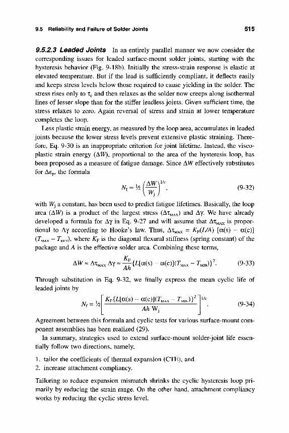
9.5 Reliability and Failure of Solder Joints 515
9.5.2.3 Leaded Joints In an entirely parallel manner we now consider the corresponding issues for leaded surface-mount solder joints, starting with the hysteresis behavior (Fig. 9-18b). Initially the stress-strain response is elastic at elevated temperature. But if the lead is sufficiently compliant, it deflects easily and keeps stress levels below those required to cause yielding in the solder. The stress rises only to Tc and then relaxes as the solder now creeps along isothermal lines of lesser slope than for the stiffer leadless joints. Given sufficient time, the stress relaxes to zero. Again reversal of stress and strain at lower temperature completes the loop.
Less plastic strain energy, as measured by the loop area, accumulates in leaded joints because the lower stress levels prevent extensive plastic straining. There-fore, Eq. 9-30 is an inappropriate criterion for joint lifetime. Instead, the visco-plastic strain energy (AW), proportional to the area of the hysteresis loop, has been proposed as a measure of fatigue damage. Since AW effectively substitutes for Acp, the formula
Nf=^^[^J\ (9-32)
with Wj a constant, has been used to predict fatigue lifetimes. Basically, the loop area (AW) is a product of the largest stress (AX^AX) and Ay. We have already developed a formula for Ay in Eq. 9-27 and will assume that AT^AX is propor-tional to Ay according to Hooke's law. Thus, AT^AX = Kp(L/A) [a(s) - a(c)] ( MAx - ^MIN). where Kj; is the diagonal flexural stiffness (spring constant) of the package and A is the effective solder area. Combining these terms,
AW - AT,AX Ay - ^{LMs) - a(c)]iT^,, - T, J } 1 (9-33)
Through substitution in Eq. 9-32, we finally express the mean cyclic life of leaded joints by
^KAL[a(s) - a(c)](r,Ax - T^MIN))' N{ = V2\
Ah Wj (9-34)
Agreement between this formula and cyclic tests for various surface-mount com-ponent assemblies has been realized (29).
In summary, strategies used to extend surface-mount solder-joint life essen-tially follow two directions, namely,
1. tailor the coefficients of thermal expansion (CTE), and 2. increase attachment compliancy.
Tailoring to reduce expansion mismatch shrinks the cyclic hysteresis loop pri-marily by reducing the strain range. On the other hand, attachment compliancy works by reducing the cyclic stress level.
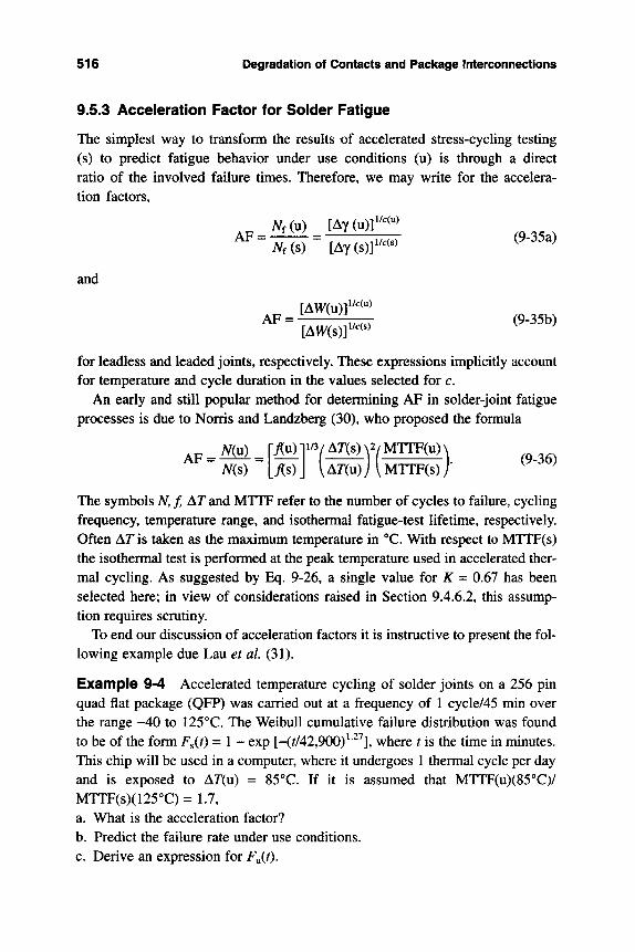
516 Degradation of Contacts and Package Interconnections
9.5.3 Acceleration Factor for Solder Fatigue
The simplest way to transform the results of accelerated stress-cycling testing (s) to predict fatigue behavior under use conditions (u) is through a direct ratio of the involved failure times. Therefore, we may write for the accelera-tion factors,
Nf(u) [AY(U)]''^^">
and
[AW(u)]'' ">
[AW(s)]' " ^
for leadless and leaded joints, respectively. These expressions implicidy account for temperature and cycle duration in the values selected for c.
An early and still popular method for determining AF in solder-joint fatigue processes is due to Norris and Landzberg (30), who proposed the formula
^ A M == ry(u)I^^Y Ar(s) \2/MTTF(u) \ (9-36)
The symbols N, f, AT and MTTF refer to the number of cycles to failure, cycling frequency, temperature range, and isothermal fatigue-test lifetime, respectively. Often AT is taken as the maximum temperature in °C. With respect to MTTF(s) the isothermal test is performed at the peak temperature used in accelerated ther-mal cycling. As suggested by Eq. 9-26, a single value for K = 0.67 has been selected here; in view of considerations raised in Section 9.4.6.2, this assump-tion requires scrutiny.
To end our discussion of acceleration factors it is instructive to present the fol-lowing example due Lau et al (31).
Example 9-4 Accelerated temperature cycling of solder joints on a 256 pin quad flat package (QFP) was carried out at a frequency of 1 cycle/45 min over the range -40 to 125°C. The Weibull cumulative failure distribution was found to be of the form F^if) = 1 - exp [-{tlA2,9QOY'^^], where t is the time in minutes. This chip will be used in a computer, where it undergoes 1 thermal cycle per day and is exposed to Ar(u) = 85°C. If it is assumed that MTTF(u)(85°C)/ MTTF(s)(125°C)=1.7, a. What is the acceleration factor? b. Predict the failure rate under use conditions. c. Derive an expression for F^{t).
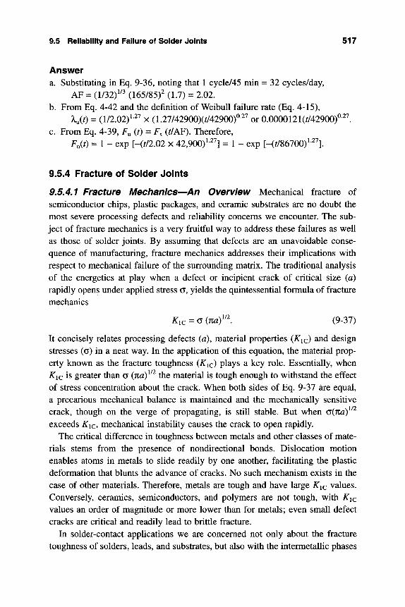
9.5 Relidbility and Failure of Solder Joints 517
Answer a. Substituting in Eq. 9-36, noting that 1 cycle/45 min = 32 cycles/day,
AF = (1/32) ^^ (165/85)^ (1.7) = 2.02. b. From Eq. 4-42 and the definition of WeibuU failure rate (Eq. 4-15),
K(t) = (1/2.02)^ ^ X (1.27/42900)(r/4290G)^-^^ or 0.0000121(^/42900)^^^. c. From Eq. 4-39, F^ (t) = F, (t/AF). Therefore,
FM = 1 - exp [-(^/2.02 X 42,900)^^^] = 1 - exp [-(f/86700)^^^].
9.5.4 Fracture of Solder Joints
9.5.4.1 Fracture Mechanics—An Overview Mechanical fracture of semiconductor chips, plastic packages, and ceramic substrates are no doubt the most severe processing defects and reliability concerns we encounter. The sub-ject of fracture mechanics is a very fruitful way to address these failures as well as those of solder joints. By assuming that defects are an unavoidable conse-quence of manufacturing, fracture mechanics addresses their implications with respect to mechanical failure of the surrounding matrix. The traditional analysis of the energetics at play when a defect or incipient crack of critical size (a) rapidly opens under applied stress a, yields the quintessential formula of fracture mechanics
K,c = o (naf\ (9-37)
It concisely relates processing defects (a), material properties (^ic) and design stresses (a) in a neat way. In the application of this equation, the material prop-erty known as the fracture toughness (KIQ) plays a key role. Essentially, when Kic is greater than a (na)^^^ the material is tough enough to withstand the effect of stress concentration about the crack. When both sides of Eq. 9-37 are equal, a precarious mechanical balance is maintained and the mechanically sensitive crack, though on the verge of propagating, is still stable. But when c(Tza)^^^ exceeds KIQ, mechanical instability causes the crack to open rapidly.
The critical difference in toughness between metals and other classes of mate-rials stems from the presence of nondirectional bonds. Dislocation motion enables atoms in metals to slide readily by one another, facilitating the plastic deformation that blunts the advance of cracks. No such mechanism exists in the case of other materials. Therefore, metals are tough and have large ^ ic values. Conversely, ceramics, semiconductors, and polymers are not tough, with Kic values an order of magnitude or more lower than for metals; even small defect cracks are critical and readily lead to brittle fracture.
In solder-contact applications we are concerned not only about the fracture toughness of solders, leads, and substrates, but also with the intermetallic phases
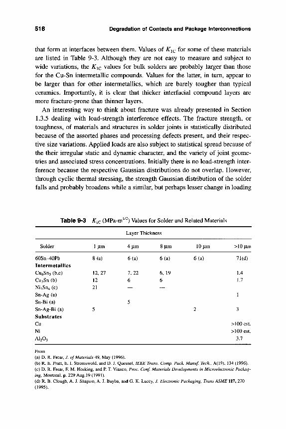
518 Degradation of Contacts and Package Interconnections
that form at interfaces between them. Values of ^ic for some of these materials are listed in Table 9-3. Although they are not easy to measure and subject to wide variations, the Kic values for bulk solders are probably larger than those for the Cu-Sn intermetallic compounds. Values for the latter, in turn, appear to be larger than for other intermetallics, which are barely tougher than typical ceramics. Importantly, it is clear that thicker interfacial compound layers are more fracture-prone than thinner layers.
An interesting way to think about fracture was already presented in Section 1.3.5 dealing with load-strength interference effects. The fracture strength, or toughness, of materials and structures in solder joints is statistically distributed because of the assorted phases and processing defects present, and their respec-tive size variations. Applied loads are also subject to statistical spread because of the their irregular static and dynamic character, and the variety of joint geome-tries and associated stress concentrations. Initially there is no load-strength inter-ference because the respective Gaussian distributions do not overlap. However, through cyclic thermal stressing, the strength Gaussian distribution of the solder falls and probably broadens while a similar, but perhaps lesser change in loading
Table 9-3 K^c (MPa-m^ ) Values for Solder and Related Materials
Layer Thickness
Solder 1 |im 4 fxm 8 \im 10 urn >10 im
60Sn-40Pb
Intermetallics
CugSns (b,c)
CugSn (b)
Ni3Sn4 (c)
Sn-Ag (a)
Sn-Bi (a)
Sn-Ag-Bi (a)
Substrates
Cu
Ni
AI2O3
8(a)
12,27
12
21
5
6(a)
7,22
6
—
5
6(a)
6, 19
6
—
6(a) 71(cl)
1.4
1.7
>100 est.
>100 est.
3.7
From (a) D. R. Frear, J. of Materials 49, May (1996). (b) R. E. Pratt, E. I. Stromswold, and D. J. Quesnel, IEEE Trans. Comp. Pack. Manuf. Tech., A(19), 134 (1996). (c) D. R. Frear, F. M. Hosking, and R T. Vianco, Proc. Conf. Materials Developments in Microelectronic Packag-ing, Montreal, p. 229 Aug. 19 (1991). (d) R. B. Clough, A. J. Shapiro, A. J. Bayba, and G. K. Lucey, J. Electronic Packaging, Trans ASME 117, 270 (1995).
9.5 Reliability and Failure of Solder Joints 519
occurs. The centroids of the two distributions approach each other, raising the probabiUty of overlap and joint fracture.
9.5.4.2 Crack Propagation Rates Cracks in solders have been reported to nucleate at solder-base metal interfaces and interfacial intermetallic compounds, as well as at highly stressed surface points (32). Once nucleated, crack propaga-tion occurs through the bulk of the solder as well as along the solder-base metal interface. Some examples of solder fractures in through-hole and surface-mount joints are reproduced in Figs. 9-20 and 9-21, respectively. These are taken from a larger collection of beautiful solder structure and failure photographs by de Kluizenaar (33). Irrespective of where it occurs, fatigue-fracture propagation has been modeled to yield the number of cycles to failure. We start by noting that at arbitrary, noncritical stress levels the stress intensity (K) is given by A'= (na)^^^ a (see Eq. 9-37). The assumption is then made that crack growth depends on some power of cyclic stress intensity range to yield the Paris equation,
-^ = B {MT = B{naT'^ (A of, (9-38) dN
where B and m are constants derived directly from experiment. Physically, the crack growth rate is necessarily proportional to the amplitude of the applied peak-to-peak stress, Aa, or difference between the maximum and minimum applied stress. Distinctions in this formula may arise depending on whether mode I (tension) or II (shear) cracks are involved. In addition, corrections for cracks of different geometries alter the constants slightly. This differential equa-tion then directly links crack growth to applied stress, material constants, and instantaneous crack size. Below the indicated stress levels for applicability of Eq. 9-38, cracks do not grow appreciably, while above them crack growth is nonlinear.
If the crack (defect) size is initially a^ the number of cycles Af required to extend it to a final length af is easily obtained by first separating variables a and A , and integrating, i.e..
rlMf ra
•>o \ B[Ac(nafY
Substitution of limits yields
The sparse amount of data on B and m values makes it difficult to apply this formula for particular solder-joint failure applications. Crack growth-rate data
Fig. 9-20 Various stages of fatigue fracture in a through-hole solder joint connecting a lead to a single-sided circuit board. From E.E. de Kluizenaar, Soldering and Surface Mount Tech 5, 56, June (1990).
520
Fig, 9-21 A collection of surface-mount solder-joint fractures, (a) Porosity at solder-lead interface, (b) Creep rupture of reflowed solder joint with lead containing a large elastic deformation.
521
Fig. 9-21 (c) General view of fatigue fracture of a soldered joint, (d) Cross-sectional view of fatigue fracture shown in Fig. 9-2Ic. From E. E. de Kluizenaar, Soldering and Surface Mount Tech 5, 56, June (1990).
522
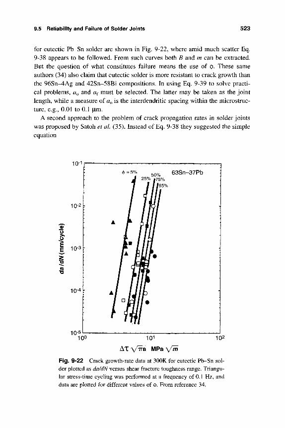
9.5 Reliability and Failure of Solder Joints 523
for eutectic Pb-Sn solder are shown in Fig. 9-22, where amid much scatter Eq. 9-38 appears to be followed. From such curves both B and m can be extracted. But the question of what constitutes failure means the use of ^. These same authors (34) also claim that eutectic solder is more resistant to crack growth than the 96Sn-^Ag and 42Sn-58Bi compositions. In using Eq. 9-39 to solve practi-cal problems, a^ and a^ must be selected. The latter may be taken as the joint length, while a measure of a^ is the interdendritic spacing within the microstruc-ture, e.g., 0.01 to 0.1 |im.
A second approach to the problem of crack propagation rates in solder joints was proposed by Satoh et al. (35). Instead of Eq. 9-38 they suggested the simple equation
10-1
10-2
o
I 10-3
10-4b
cj) = 5% 5Q,/ 63Sn-37Pb 25% |75%
/95%
10-51 100
AT
101
ira MPa
102
m Fig. 9-22 Crack growth-rate data at 300K for eutectic Pb-Sn sol-der plotted as da/dN versus shear fracture toughness range. Triangu-lar stress-time cycling was performed at a frequency of 0.1 Hz, and data are plotted for different values of (|). From reference 34.
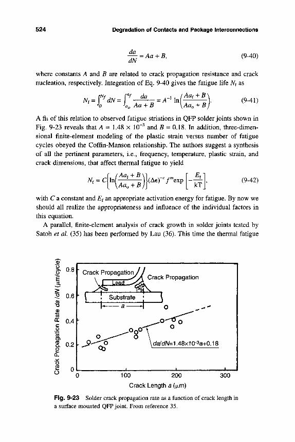
524 Degradation of Contacts and Package Interconnections
da
dN = A a + J5, (9-40)
where constants A and B are related to crack propagat ion resistance and crack
nucleat ion, respectively. Integration of Eq . 9-40 gives the fatigue life A f as
eNf f^f da 1 lAaf + B\ ^ = \fdN^\ -T^^ = A-'\ri[—^—-\ (9-41)
^0 Ja^Aa-^B \Aao + B)
A fit of this relation to observed fatigue striations in QFP solder joints shown in Fig. 9-23 reveals that A = 1.48 x 10"^ and 5 = 0.18. In addition, three-dimen-sional finite-element modeling of the plastic strain versus number of fatigue cycles obeyed the Coffin-Manson relationship. The authors suggest a synthesis of all the pertinent parameters, i.e., frequency, temperature, plastic strain, and crack dimensions, that affect thermal fatigue to yield
Nf=C\ Inl Aaf + B
Aa, o + Bjl (Ae r / ^exp
kT (9-42)
with C a constant and Ef an appropriate activation energy for fatigue. By now we should all realize the appropriateness and influence of the individual factors in this equation.
A parallel, finite-element analysis of crack growth in solder joints tested by Satoh et al. (35) has been performed by Lau (36). This time the thermal fatigue
.2
B cc. c g
a. o
o
O
0.8 h
0.6 r
0.4
0.2 h
Crack Propagation// \ -^A Crack Propagation
ofa/c/A/=1.48x10-3a+0.18
100 200
Crack Lengtii a (jxm)
300
Fig. 9-23 Solder crack propagation rate as a function of crack length in a surface mounted QFP joint. From reference 35.
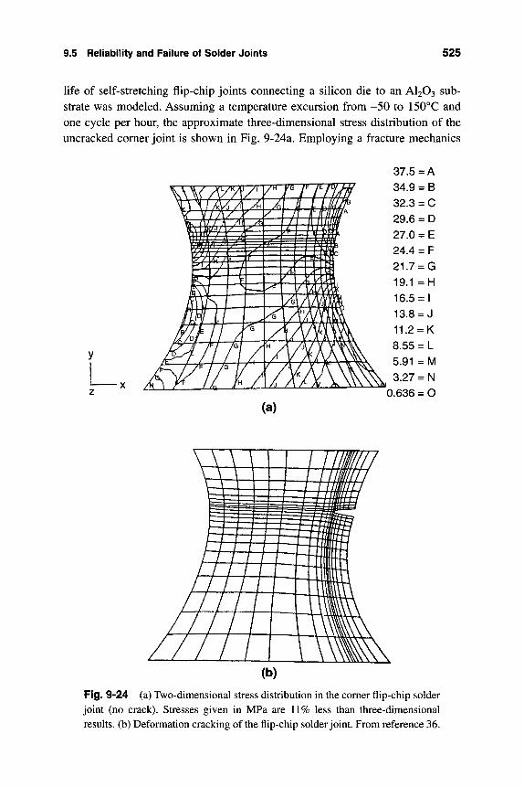
9.5 Reliability and Failure of Solder Joints 525
life of self-stretching flip-chip joints connecting a silicon die to an AI2O3 sub-strate was modeled. Assuming a temperature excursion from -50 to 150°C and one cycle per hour, the approximate three-dimensional stress distribution of the uncracked comer joint is shown in Fig. 9-24a. Employing a fracture mechanics
Fig. 9-24 (a) Two-dimensional stress distribution in the comer flip-chip solder joint (no crack). Stresses given in MPa are 11% less than three-dimensional results, (b) Deformation cracking of the flip-chip solder joint. From reference 36.
526 Degradation of Contacts and Package Interconnections
approach, failure of the cracked joint (Fig. 9-24b) was predicted to occur in 3000 cycles. This estimate compared well with the experimentally observed 2700 cycle failure life. Significantly, but perhaps fortuitously, thermal fatigue life pre-diction by both fracture mechanics and Coffin-Manson approaches were in good agreement.
9.6 DYNAI\/IIC LOADING EFFECTS IN ELECTRONIC EQUIPMENT
9.6.1 Introduction
We now address some other reliability concerns that stem from periodic stress-ing of structures and components. Rather than cyclic stresses arising from ther-mal expansion mismatch, external dynamic loading and the resultant displace-ments they produce in electronic hardware are of interest now. Electronic equipment is subject to many different forms of vibration over wide frequency ranges and acceleration levels (37). These include dynamic-loading effects such as impact, shock, and acoustic noise by the action of cooling fans, repeated impact of keys during typing, accidental misuse, and vibration surrounding mil-itary activities, etc. The kinds of failure that result are due to flexure of circuit boards, fatigue, loosening and even opening of contacts, and the shorting of leads, attached components, and devices. Complete loosening of screw and nut fasteners due to vibration can eventually cause them to rattle around inside equipment with the potential for producing serious damage. Loosening is an interesting phenomenon that is not entirely understood. Apparently, the dynamic loading stretches the bolt, momentarily reducing the friction between the nut and threads; after it unwinds a bit, the bolt relaxes, retightening the nut. This cyclic action is the driving force that causes fasteners to loosen; when they do, electri-cal contact (e.g., grounding) may be lost.
Characteristics that distinguish dynamically generated from thermal-mismatch-induced damage include:
1. Thermal-mismatch damage and failure is more common and a greater relia-bility concern. Vibrational stresses tend to be small by comparison.
2. Dynamic-loading effects influence the mechanical reliability of second (e.g., circuit boards, leads) and third (e.g., board contacts, ground planes) levels of packaging more than chip-level structures and components.
3. External rather than internal stresses are the sources of damage. 4. Dynamic effects occur and are modeled at constant temperature, e.g., room
temperature.
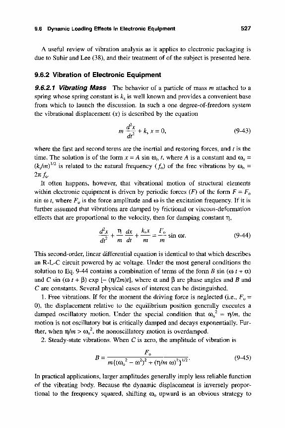
9.6 Dynamic Loading Effects in Electronic Equipment 527
A useful review of vibration analysis as it applies to electronic packaging is due to Suhir and Lee (38), and their treatment of of the subject is presented here.
9.6.2 Vibration of Eiectronic Equipment
9,6.2.1 Vibrating iViass The behavior of a particle of mass m attached to a spring whose spring constant is k^ is well known and provides a convenient base from which to launch the discussion. In such a one degree-of-freedom system the vibrational displacement (jc) is described by the equation
m ^ + k,x = 0, (9-43)
where the first and second terms are the inertial and restoring forces, and t is the time. The solution is of the form x = A sin COQ t, where A is a constant and cOo = ikjm)^'^ is related to the natural frequency (/o) of the free vibrations by cOo =
It often happens, however, that vibrational motion of structural elements within electronic equipment is driven by periodic forces (F) of the form F = F^ sin CO t, where F^ is the force amplitude and co is the excitation frequency. If it is further assumed that vibrations are damped by frictional or viscous-deformation effects that are proportional to the velocity, then for damping constant tj,
cfx r| dx Kx Fo . ,^ ^^, —r- + -H — = — sm cor. (9-44) dt m at m m
This second-order, linear differential equation is identical to that which describes an R-L-C circuit powered by ac voltage. Under the most general conditions the solution to Eq. 9-44 contains a combination of terms of the form B sin (co ? + a) and C sin (co r H- p) exp [- (r|/2m)fl, where a and p are phase angles and B and C are constants. Several physical cases of interest can be distinguished.
1. Free vibrations. If for the moment the driving force is neglected (i.e., FQ = 0), the displacement relative to the equilibrium position generally executes a damped oscillatory motion. Under the special condition that COQ = r\/m, the motion is not oscillatory but is critically damped and decays exponentially. Fur-ther, when r\/m > cOo , the nonoscillatory motion is overdamped.
2. Steady-state vibrations. When C is zero, the amplitude of vibration is
^ o
^ " m{(cOo' - co ) + di/m co) } ^ * ^^"^^^
In practical applications, larger amplitudes generally imply less reliable function of the vibrating body. Because the dynamic displacement is inversely propor-tional to the frequency squared, shifting cOo upward is an obvious strategy to
528 Degradation of Contacts and Package interconnections
limit vibration. It is instructive to compare B with the static displacement of the mass, JCs = FJks under constant load F^. The ratio B/x^, which is known as the amplification factor A, is then given by
^s 1 m{(cOo - co ) + (Ti/m co) }^^ ' {(1 - co^W)^ + [Ti/m((o/cOo) ]} ^ '
Among the possible behaviors are the following:
1. When cOo > CO, A « 1. In this case, the amplitude of forced vibrations is equal to that of the static displacement.
2. If CO « cOo, A reaches its largest value of [r|/m]~^^ . This is the resonant condi-tion, a state that should be avoided because dynamic loads and stresses are magnified.
3. When co » COQ, A « (COQ/CO) . Thus at very high applied frequencies, A approaches zero, and the system is relatively immune to vibrational damage.
9.6.2,2 Vibration of Beams Instead of the point masses above, we now consider the vibration of components that can be idealized as beams. The result-ing vibrations cause transverse displacements u(x, t) normal to the beam, or x-axis, that obey the partial differential equation (39)
rrid^ W(JC, 0 Eldl^ u(x, t)
dt" 9 / (9-46)
Here u = u(x, t) is the displacement function, E is Young's modulus of the mate-rial, / is the moment of inertia of the beam cross-section {EI is the flexural rigid-ity), and m is the mass per unit length. General solutions for the natural fre-quencies of vibration are
where the value of K^ depends on the particular boundary conditions. Several specific beam geometries are shown in Fig. 9-25, where corresponding K^ val-ues are given. For example, if the beam is freely supported or hinged at oppos-ing ends (Fig. 9-23a), the displacements are those of the simple vibrating string. In this case Kn = (n nf, where n is an integer 1, 2, 3, . . . that denotes the first, second, third, . . . mode of vibration. Normally we are interested only in the first mode, because its vibrational amplitude exceeds that of the other modes.
From the standpoint of reliability, low-frequency oscillations should be avoided because they lead to large vibrational amplitudes. Therefore, other
9.6 Dynamic Loading Effects in Electronic Equipment 529
El,m
—I-
(a)
(c)
/ X2= sin 2iTX
X3= sin32ix
(b)
(d)
Fig. 9-25 Vibrational frequencies (271/„ = „[£//m/ ] ^ ) of various beams. (a) cantilever; ifTi = 3.516, ^2 = 22.04, ^„ = {(2n-f-1)71/2} for« = 3,4, . . . . (b) freely supported (hinged at both ends); ^i = 9.870, K2 = 39.48, K„ = (n nf for« = 3,4, . . . .(c) clamped-hinged;i^i = 15.42, i5:2 = 49.96, J „ = {(4n + l)7C/2} for n = 3, 4, . . . . (d) clamped at both ends; K^ = 22.37, i 2 = 61.67,/i:„={(2n +1)71/2}^ for n = 3,4, . . . . From reference 38.
things being equal, stiffening the beam or board, reducing its mass and sectional area, and particularly, shortening its length, will all help to bring about the desideratum of higher-frequency vibrational modes. Clamping beams at either one or both ends also raises the vibrational frequencies. Electronic components whose geometry and structural behavior can be idealized as a cantilever are least desirable from the standpoint of mechanical reliability. This situation occurs in circuit boards plugged in or clamped at only one end. A simple comparison of the structures depicted in Fig. 9-25 shows that cantilevers vibrate at the lowest frequencies.
9.6.2.3 Vibration of Pacliaging Components The formulas just pre-sented apply equally well to elongated plates such as long, narrow printed circuit boards. But in order to use them, EI in Eq. 9-47 must be replaced by the flexural rigidity of the plate, i.e., Eh^/[12(1 - v^)], where 8 is the plate thickness. For wide plates of dimension IxW, the formula that applies is
u3
fn = -Eh'
In 1 12 (1 - v^)m{f + W )
1/2 (9-48)
where the mass is now on a per unit area basis. If the plate is simply supported, K^ = 9.87.
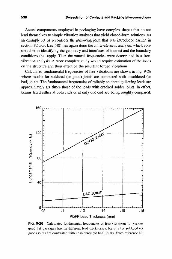
530 Degradation of Contacts and Package Interconnections
Actual components employed in packaging have complex shapes that do not lend themselves to simple vibration analyses that yield closed-form solutions. As an example let us reconsider the gull-wing joint that was introduced earlier, in section 8.5.3.3. Lau (40) has again done the finite-element analysis, which con-sists first in identifying the geometry and interfaces of interest and the boundary conditions that apply. Then the natural frequencies were determined in a free-vibration analysis. A more complete study would require estimation of the loads on the structure and their effect on the resultant forced vibrations.
Calculated fundamental frequencies of free vibrations are shown in Fig. 9-26 where results for soldered (or good) joints are contrasted with unsoldered (or bad) joints. The fundamental frequencies of reliably soldered gull-wing leads are approximately six times those of the leads with cracked solder joints. In effect, beams fixed either at both ends or at only one end are being roughly compared;
160
N X
c 0 13 CT
120
^ 80
0)
E CO
• D
c 3 40
r-TTT-rT-rr r r
P
l^
" i 1 • 1 1 1 1 . 1
1 1 1 1 1 1 1 1 1
1 1 1 1 1 • • i . i . i .
1 1 1 1 j 1 1 1 1
BAD JOINT
. t > > 1 • . • 1
1 ' ' ' ' 1 ' ' ' '
{
1 1 1 . I 1 1 1 1
j 1 I 1 1 j 1 1 I M
' J
H
1 1 1 1 1 1 ii I 1 1
.08 .12 .14
PQFP Lead Thickness (mm)
.15 .18
Fig. 9-26 Calculated fundamental frequencies of free vibrations for various quad flat packages having different lead thicknesses. Results for soldered (or good) joints are contrasted with unsoldered (or bad) joints. From reference 40.
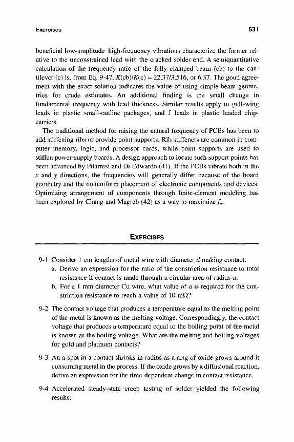
Exercises 531
beneficial low-amplitude-high-frequency vibrations characterize the former rel-ative to the unconstrained lead with the cracked solder end. A semiquantitative calculation of the frequency ratio of the fully clamped beam (cb) to the can-tilever (c) is, from Eq. 9-47, K(cb)/K(c) = 22.37/3.516, or 6.37. The good agree-ment with the exact solution indicates the value of using simple beam geome-tries for crude estimates. An additional finding is the small change in fundamental frequency with lead thickness. Similar results apply to gull-wing leads in plastic small-outline packages, and J leads in plastic leaded chip-carriers.
The traditional method for raising the natural frequency of PCBs has been to add stiffening ribs or provide point supports. Rib stiffeners are common in com-puter memory, logic, and processor cards, while point supports are used to stiffen power-supply boards. A design approach to locate such support points has been advanced by Pitarresi and Di Edwardo (41). If the PCBs vibrate both in the X and y directions, the frequencies will generally differ because of the board geometry and the nonuniform placement of electronic components and devices. Optimizing arrangement of components through finite-element modeling has been explored by Chang and Magreb (42) as a way to maximize /„.
EXERCISES
9-1 Consider 1 cm lengths of metal wire with diameter d making contact. a. Derive an expression for the ratio of the constriction resistance to total
resistance if contact is made through a circular area of radius a. b. For a 1 mm diameter Cu wire, what value of a is required for the con-
striction resistance to reach a value of 10 mQ?
9-2 The contact voltage that produces a temperature equal to the melting point of the metal is known as the melting voltage. Correspondingly, the contact voltage that produces a temperature equal to the boiling point of the metal is known as the boiling voltage. What are the melting and boiling voltages for gold and platinum contacts?
9-3 An a-spot in a contact shrinks in radius as a ring of oxide grows around it consuming metal in the process. If the oxide grows by a diffusional reaction, derive an expression for the time-dependent change in contact resistance.
9-4 Accelerated steady-state creep testing of solder yielded the following results:
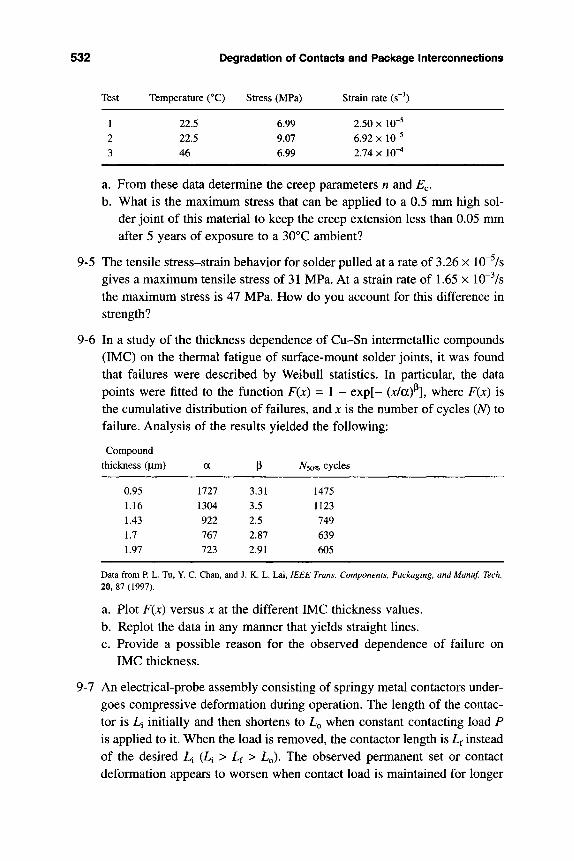
532 Degradation of Contacts and Package Interconnections
Test
1
2
3
Temperature (°C)
22.5
22.5
46
Stress (MPa)
6.99
9.07
6.99
Strain rate (s )
2.50 X 10"^
6.92 X 10"^
2.74 X 10"^
a. From these data determine the creep parameters n and Ec. b. What is the maximum stress that can be appHed to a 0.5 nmi high sol-
der joint of this material to keep the creep extension less than 0.05 mm after 5 years of exposure to a 30°C ambient?
9-5 The tensile stress-strain behavior for solder pulled at a rate of 3.26 x 10~ /s gives a maximum tensile stress of 31 MPa. At a strain rate of 1.65 x 10~Vs the maximum stress is 47 MPa. How do you account for this difference in strength?
9-6 In a study of the thickness dependence of Cu-Sn intermetallic compounds (IMC) on the thermal fatigue of surface-mount solder joints, it was found that failures were described by WeibuU statistics. In particular, the data points were fitted to the function F(x) = 1 - exp[- (x/a)\ where F(x) is the cumulative distribution of failures, and x is the number of cycles (AO to failure. Analysis of the results yielded the following:
Compound
thickness (p.m)
0.95
1.16
1.43
1.7
1.97
a
1727
1304
922
767
723
P 3.31
3.5
2.5
2.87
2.91
A 5o% eye
1475
1123
749
639
605
Data from P. L. Tu, Y. C. Chan, and J. K. L. Lai, IEEE Trans. Components, Packaging, and Manuf. Tech. 20, 87 (1997).
a. Plot F{x) versus x at the different IMC thickness values. b. Replot the data in any manner that yields straight lines. c. Provide a possible reason for the observed dependence of failure on
IMC thickness.
9-7 An electrical-probe assembly consisting of springy metal contactors under-goes compressive deformation during operation. The length of the contac-tor is Li initially and then shortens to LQ when constant contacting load P is applied to it. When the load is removed, the contactor length is Lf instead of the desired L^ m > Lf > LQ). The observed permanent set or contact deformation appears to worsen when contact load is maintained for longer
Exercises 533
time, or if the contact tips get hot. Provide an explanation for these effects and mention the material properties you would recommend for set-free contact behavior.
9-8 A leadless chip carrier soldered to a circuit board is thermally fatigued by turning the board on and off three times a day. Each cycle requires 30 min-utes to reach the steady-state operating temperature of 50°C. Predict how many cycles the eutectic solder can sustain prior to failure if the strain in each cycle is 0.005.
9-9 Cracks in copper-plated through-holes were observed to grow during ther-mal cycling. The crack length (2a) varied with the number of cycles (AO as 2fl = 1.16 X 10~ ^ A ^ . Derive expressions for a. da/dN as a function of A . b. da/dN as a function of a. c. da/dN as a function of A^.
9-10 A high-power resistor is soldered at each end close to a PCB by means of solder posts. During operation, heat is emitted by the resistor. Discuss how the PCB warps in response.
9-11 A leadless ceramic chip carrier is soldered to an FR4 printed circuit board and thermally cycled between 0°C to 100°C, with 20 minute dwells at the maximum temperature. The chip carrier measures 0.635 cm x 0.635 cm and the joints are 0.013 cm high. If the CTE for the ceramic is 6 x 10"^ and that for FR4 is 12 x 10"^ °C~\ predict how many cycles will be sustained prior to failure?
9-12 It is desired that an electronic assembly, consisting of a chip carrier bonded through a fully compliant solder to a substrate, operate at a chip tempera-ture Tc and a substrate temperature Tg, where T^ > T^. To minimize the shear strain produced in heating the chip from T^ from T^, and the substrate from To from T^, what value of thermal expansion coefficient (a^) would you recommend? The chip has a thermal expansion coefficient of ac.
9-13 Eutectic solder fatigued at 25°C and 10 Hz displayed a crack-growth dependence on the number of cycles given by da/dN = 2.77 x 10"^ AK^'^^, where AK has units of MPa-m^^ . A ball-bond joint composed of this sol-der was subjected to fatigue loading, and finite-element analysis revealed that AK depends linearly on crack length. Specifically, A^ =0.151 MPa-m^^^ at the initial crack length of 5.65 x 10"^ m, and AJ = 0.261 MPa-m^^^ at a crack length of 1.02 x 10"^ m corresponding to joint fracture, a. How many cycles did the solder sustain prior to fatigue failure?
534 Degradation of Contacts and Package Interconnections
b. If the joint is cycled once per hour and reaches a maximum temperature of 150°C, estimate how long it will take for the solder to fail.
9-14 At the 1996 Surface Mount International Conference it was reported that plastic ball-grid array (PBGA) solder joints whose solder balls contained void defects (up to 24% of the pad area) had no adverse effect on board-level reliability; "In fact, PGBA solder joints with voids had 16 percent better reliability than those without voids" ! a. What are the likely sources of voids in freshly soldered joints? b. Provide scientific explanations for these paradoxical findings.
9-15 Suppose incandescent-bulb life is governed by low-cycle thermal fatigue. The thermal strain is induced by a 2000°C rise or drop in the tungsten-fil-ament temperature each time the bulb is turned on or off, respectively. If the equation governing lamp life is A f^ Acp = 0.2, predict the number of cycles to failure.
9-16 Calculate the natural frequency of a vibrating cantilever spring that is loaded at the free end.
9-17 A simply supported beam of length L with a concentrated load P at the center exhibits a deflection given by 6 = PL^I{A^EI). If such a beam can be simulated as a spring-mass system, calculate the natural frequency of vibration.
9-18 Experience shows that actual resonant frequencies of vibrating beams are lower than those theoretically calculated. Suggest a reason why this is so.
9-19 Rapid variations in the temperature of packages can theoretically induce stress because of the acceleration forces associated with dimensional changes. Consider a 30 mm long package of specific gravity 2 that is 10 mm wide and 1 mm thick. If the package undergoes a temperature rise of 100°C in 0.1 sec, what is the stress from this source? How does this value compare with typical thermal stresses?
9-20 A vibration test was conducted on circuit cards installed within a computer mainframe. The cards lay in the horizontal plane cantilevered off the moth-erboard. In ramping the frequency up to 60 Hz one of the circuit cards began to vibrate excessively at 50Hz. The involved card made of fiberglass {E = 38GPa), weighs 80 grams and is 30 cm long, 3 cm wide and 0.1 cm thick. How thick should the card be to displace the first mode of vibration to 120Hz? Mention another way to increase the vibrational frequency of the card.
References 535
9-21 Determine the resonant frequency of a rectangular plug-in circuit card assembly that is simply supported on all four sides. The epoxy-glass printed circuit board weighs 0.545 kg, has dimensions of 22.9 cm x 17.8 cm X 0.2 cm and elastic properties defined by £" = 14 GPa and Poisson's ratio of 0.12.
REFERENCES
1. R. Holm, Electrical Contacts-Theory and Applications, 4th ed.. Springer Verlag, New York (1967).
2. F. Llewellyn Jones, The Physics of Electrical Contacts, Clarendon Press, Oxford (1957).
3. M. Braunovic', Proc. 40th IEEE Holm Conf. on Electrical Contacts, p. 1, (1994).
4. M. Runde, IEEE Trans. Components, Hybrids and Manuf. Tech., CHMT-10, 89 (1987).
5. M. Runde, H. Kongjorden, J. Kulsetas, and B. Todtal, IEEE Trans. Compo-nents, Hybrids and Manuf. Tech., CHMT-9, 11 (1986).
6. R. S. Mroczkowski, Proc. First Electronic Materials and Processing Con-gress, p. 159, Chicago, Sept. 24-30 (1988).
7. N. A. Stennett, T. P. Ireland, and D. S. Campbell, IEEE Trans.Components, Hybrids and Manuf Tech. 14, 45 (1991).
8. N. A. Stennett and D. S. Campbell, IEEE Trans.Components, Packaging and Manuf Tech. 17A, 128 (1994).
9. P A. Engel, IEEE Trans, on Reliability 42 (2), 262 (1993). 10. J. F. Archard, /. Appl. Phys. 24, 981 (1953). 11. M. Antler, IEEE Trans. Components, Hybrids and Manuf. Tech. 8, 87
(1985). 12. M. Antler, IEEE Circuits and Devices 3, 8 March (1987). 13. M. Braunovic', IEEE Trans. Components, Hybrids and Manuf. Tech. 15,
205 (1992). 14. M. D. Bryant, IEEE Trans. Components, Packaging and Manuf Tech. 17,
86 (1994). 15. J. H. Lau, in Thermal Stress and Strain in Microelectronics Packaging, ed.
J. H. Lau, Van Nostrand Reinhold, New York (1993). 16. J. H. Lau, ed.. Solder Joint Reliability, Van Nostrand Reinhold, New York
(1991).
536 Degradation of Contacts and Package Interconnections
17. J. H. Lau, ed., Thermal Stress and Strain in Microelectronics Packaging, Van Nostrand Reinhold, New York (1993).
18. R. Darveaux and K. Banerji, IEEE Trans. Components, Hybrids andManuf. Tech 15, 1013 (1992).
19. J. H. Lau, Soldering and Surface Mount Tech. 13, 45, Oct. (1993). 20. Z. Guo, Y.-H. Pao, and H. Conrad, J. Electronic Packaging, Trans AIME
111, 100, June (1995). 21. G. F. Dieter, Mechanical Metallurgy, 3rd ed., McGraw-Hill, New York
(1986). 22. D. F. Socie, M. R. Mitchell, and E. M. Caulfield, Fundamentals of Modem
Fatigue Analysis, FCP Report No. 26, U of Illinois (1978). 23. H. D. Solomon in Solder Joint Reliability, ed. J. H. Lau, Van Nostrand Rein-
hold, New York (1991). 24. L. R Coffin, ASTM-STP 520, 5 (1973). 25. M. Ohring, Engineering Materials Science, p. 340, Academic Press, San
Diego (1995). 26. W. Engelmaier, in Solder Joint Reliability, ed. J. H. Lau,, Van Nostrand
Reinhold, New York (1991). 27. W. Engelmaier, Soldering and Surface Mount Tech., No. 1, 14, Feb. (1989). 28. J.-P.M. Clech and J.A. Augis, in Solder Joint Reliability, ed. J. H. Lau, Van
Nostrand Reinhold, New York (1991). 29. J. W. Balde, IEEE Trans. Components, Hybrids and Manuf Tech. 10, 463
(1987). 30. K. C. Norris and A. H. Landzberg, IBM J. Res. and Develop. 13,266 (1969). 31. J. H. Lau, Y.-H. Pao, C. Lamer, R. Govila, S. Twerefour, D. Gilbert, E. Eras-
mus, and S. Dolot, Soldering and Surface Mount Tech 16, 42, Feb. (1994). 32. R. B. Clough, A. J. Shapiro, A. J. Bayba, and G.K. Lucey, / Electronic
Packaging, Trans ASME 111, 270 (1995). 33. E. E. de Kluizenaar, Soldering and Surface Mount Tech 4, 27, Feb. (1990).
and E. E. de Kluizenaar, Soldering and Surface Mount Tech 5, 56, June (1990).
34. Z. Guo, A. F. Sprecher, H. Conrad, and M. Kim, Proc. Conf. Materials Developments in Microelectronic Packaging, Montreal, p. 155, Aug. (1991).
35. R. Satoh, K. Arakawa, M. Harada and K. Matsui, IEEE Trans. Components, Hybrids andManuf Tech. 14 (1), 224 (1991).
36. J. H. Lau, ed.. Flip Chip Technologies, McGraw Hill, New York (1996). 37. D. S. Steinberg, Vibration Analysis for Electronic Equipment, 2nd ed, Wiley,
New York (1988). 38. E. Suhir and Y C. Lee, in Electronic Materials Handbook, Volume I, Pack-
aging, p. 45. ASM International, Materials Park, OH (1989).
References 537
39. M. Paz, Structural Dynamics, Van Nostrand Reinhold, New York (1982). 40. J. H. Lau, in Solder Joint Reliability ed. J. H. Lau, Van Nostrand Reinhold,
New York (1993). 41. J. M. Pitarresi and A. V. Di Edwardo, /. Electronic Packaging, Trans ASME
115, 119 (1993). 42. T.-S. Chang and E. B. Magreb, J. Electronic Packaging, Trans ASME 115,
312(1993).

This Page Intentionally Left Blank
Chapter 10
Degradation and Failure of Electro-optical Materials
and Devices
10.1 INTRODUCTION
Together with microelectronics, optoelectronics (or electro-optics) is transform-ing our lives and helping to shape a future based on high technology. This is evi-dent from the dominant role of optical materials and devices in some of the most important arenas of human activity, e.g., fibers for optical communications; lasers and imaging systems for medical applications; optical sensors for a host of industrial processing, control and testing applications; lenses, filters; and opti-cally active materials for observing, detecting, displaying, and recording images in microscopy, photography, media, and information systems.
Optical materials can be broadly divided into two categories—active and pas-sive. The active category includes those materials that exhibit special optical properties in response to electrical, magnetic, mechanical, optical, and thermal signals and interactions. Examples based on semiconductors include light sources such as lasers and light-emitting diodes, and photodiode detectors. In addition, there are magneto-optical recording media, luminescent materials, polymer photoresists, and liquid crystal displays that are not based on semicon-ductors. Passive optical materials transmit and reflect the light in components such as lenses, waveguides, and optical coatings. The same material can be used in active and passive applications. For example, silicon is active in a solar cell
539
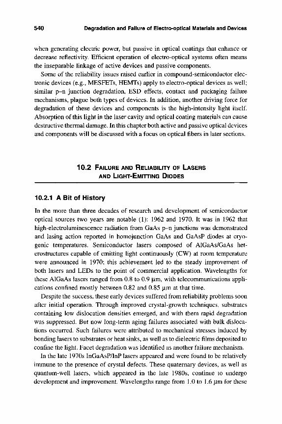
540 Degradation and Failure of Electro-optical Materials and Devices
when generating electric power, but passive in optical coatings that enhance or decrease reflectivity. Efficient operation of electro-optical systems often means the inseparable linkage of active devices and passive components.
Some of the reliability issues raised earlier in compound-semiconductor elec-tronic devices (e.g., MESFETs, HEMTs) apply to electro-optical devices as well; similar p-n junction degradation, ESD effects, contact and packaging failure mechanisms, plague both types of devices. In addition, another driving force for degradation of these devices and components is the high-intensity light itself. Absorption of this light in the laser cavity and optical coating materials can cause destructive thermal damage. In this chapter both active and passive optical devices and components will be discussed with a focus on optical fibers in later sections.
10.2 FAILURE AND RELIABILITY OF LASERS
AND LIGHT-EMITTING DIODES
10.2.1 A Bit of History
In the more than three decades of research and development of semiconductor optical sources two years are notable (1): 1962 and 1970. It was in 1962 that high-electroluminescence radiation from GaAs p-n junctions was demonstrated and lasing action reported in homojunction GaAs and GaAsP diodes at cryo-genic temperatures. Semiconductor lasers composed of AlGaAs/GaAs het-erostructures capable of emitting light continuously (CW) at room temperature were announced in 1970; this achievement led to the steady improvement of both lasers and LEDs to the point of commercial application. Wavelengths for these AlGaAs lasers ranged from 0.8 to 0.9 |Lim, with telecommunications appli-cations confined mostly between 0.82 and 0.85 jLim at that time.
Despite the success, these early devices suffered from reliability problems soon after initial operation. Through improved crystal-growth techniques, substrates containing low dislocation densities emerged, and with them rapid degradation was suppressed. But now long-term aging failures associated with bulk disloca-tions occurred. Such failures were attributed to mechanical stresses induced by bonding lasers to substrates or heat sinks, as well as to dielectric films deposited to confine the light. Facet degradation was identified as another failure mechanism.
In the late 1970s InGaAsP/InP lasers appeared and were found to be relatively inmiune to the presence of crystal defects. These quaternary devices, as well as quantum-well lasers, which appeared in the late 1980s, continue to undergo development and improvement. Wavelengths range from 1.0 to 1.6 |Lim for these
10.2 Failure and Reliability of Lasers and Light-Emitting Diodes 541
InGaAsP lasers, with telecommunications applications limited either to 1.3 or to 1.55 |xm.
The reliability of lasers and LEDs have greatly improved in the past two decades. Nowadays LED technology produces devices whose optical output declines by only 5 to 20% after -10^ hours at 55°C, and half brightness is not reached in -10^ hours at ambient temperatures. In most applications involving a human interface, a factor of two in degradation is not noticeable (2). Most of these LEDs are based on GaAs or InP technology, which generally means long-wavelength visible (red) and invisible infrared output. However, in the short wavelength, or blue region of the spectrum, there had been a long-standing need for reliable LEDs and lasers. Finally, in 1994 Nichia Chemical Industries intro-duced blue LEDs based on GaN that were 100 times brighter than SiC LEDs. In one of the first studies on the reliability of these devices it was found that despite a high imperfection density that would have proved fatal to GaAs and InP LEDs, defects in GaN diodes are immobile (3).
Reliability issues in these electro-optical devices are not limited only to semi-conductors. For example, telecommunications lasers are usually packaged within modules that may contain a monitor photodiode (to control light output), an opti-cal isolator (to prevent back reflection of light), a thermoelectric cooler, a tem-perature sensor, circuitry for operating the laser, lenses, and optical fiber. Over-all reliability of the laser module implies trouble-free functioning of these components as well. And just as in the case in IC chips, the reliability of lasers is influenced by the quality of the packaging materials.
10.2.2 Reliability Testing of Lasers and LEDs
Accelerated life tests are the most popular way to assess the reliability of lasers and LEDs. For this purpose constant current (input) and constant light (output) accelerated aging tests are performed. For lasers, degradation is usually tracked by measuring the increased threshold current with time or by monitoring the current required for a specified light output. On the other hand, the decrease in output-light power (at fixed current) with time is usually taken as a measure of degradation in LEDs. The distinction between these two kinds of accelerated test data is shown in Figs. 10-la and b.
10.2.2.1 Constant Light Output-Power Testing Laser operating charac-teristics shown in Fig. 2-27 (and rotated 90° in Fig. 10-la) are the basis of both pass/fail qualification as well as degradation testing. Nash (4), in an extensive failure testing program on lasers employed in undersea optical-conmiunications systems, has addressed the thorny issues of:
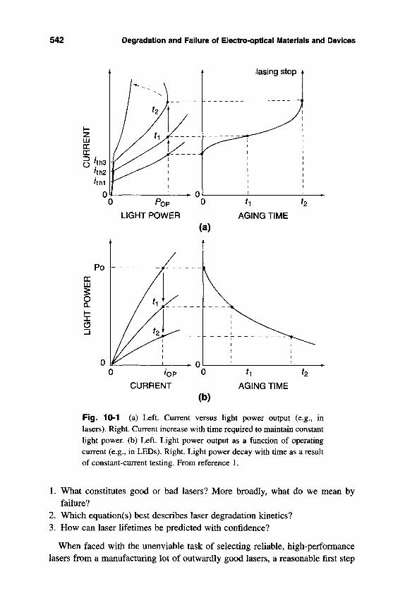
542 Degradation and Failure of Eiectro-opticai IMateriats and Devices
LU CL DC 3 O 'th3
'th2 'th1
0
M / 7
^
I
i
: ^ _ . .
0
lasing stop .
•
LIGHT POWER AGING TIME
(a)
Po DC LU
o Q. I -X o
i
/ u
/ K
,
^„.^
0
.
1 1
\ ^ 'OP
CURRENT
0
(b)
AGING TIME
Fig. 10-1 (a) Left. Current versus light power output (e.g., in lasers). Right. Current increase with time required to maintain constant light power, (b) Left. Light power output as a function of operating current (e.g., in LEDs). Right. Light power decay with time as a result of constant-current testing. From reference 1.
L What constitutes good or bad lasers? More broadly, what do we mean by failure?
2. Which equation(s) best describes laser degradation kinetics? 3. How can laser lifetimes be predicted with confidence?
When faced with the unenviable task of selecting reliable, high-performance lasers from a manufacturing lot of outwardly good lasers, a reasonable first step
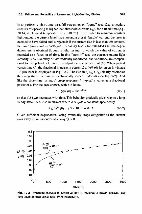
10.2 Failure and Reliability of Lasers and Light-Emitting Diodes 543
is to perform a short-time pass/fail screening, or "purge" test. One procedure consists of operating at higher than threshold currents (/th). for a fixed time (e.g., 18 h), at elevated temperature (e.g., 100°C). If, in order to maintain constant light output, the current level rises beyond a preset "hurdle" current, the laser is deemed to have failed and is rejected; if the current rise is less than this amount, the laser passes and is packaged. To qualify lasers for extended use, the degra-dation rate is obtained through similar testing, in which the value of current is recorded as a function of time. In this "bum-in" test, the constant-output light intensity is continuously or intermittently monitored, and variations are compen-sated for using feedback circuits to adjust the injected current (ii). When plotted versus time ( 0 , ^ e fractional increase in current A iiit)/iiiO) for an early vintage 1.3 |xm laser is displayed in Fig. 10-2. The rise in /L ( t > th) clearly resembles the creep strain increase in mechanically loaded materials (see Fig. 9-7). And like the short-time (primary) creep response, /L typically varies as a fractional power of t. For the case shown, with t in hours.
A/L(0/t(0) = O.Olf ,0.25 (10-1)
so that d A /L/< t decreases with time. This behavior gradually gives way to a long steady-state linear rise in current where d A ijdt = constant; specifically,
A /L(0/?'L(0) = 8.5 X 10"^ t + 0.05. (10-2)
Given sufficient degradation, lasing eventually stops altogether as the current runs away in an uncontrollable way ^ > 0.
0.1
0.09
0.08
0.07 f-
ML (t) 0.06
/L(0) 0.05
0.04
0.03
0.02
0.01
0 500 1000 1500
TIME (h)
2000 2500 3000
Fig. 10-2 Fractional increase in current AiiXt)/ii^(0) required to sustain constant laser light output plotted versus time. From reference 4.
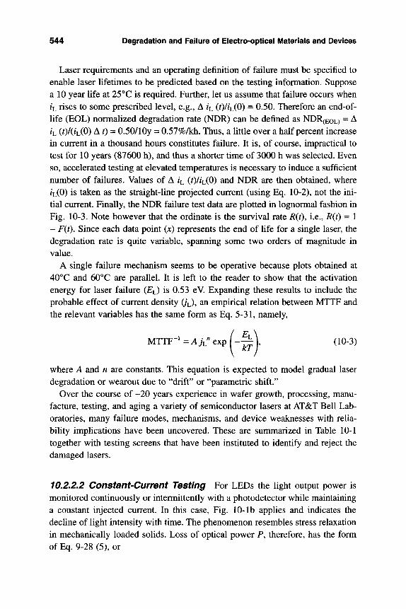
544 Degradation and Failure of Electro-optical l\/laterlals and Devices
Laser requirements and an operating definition of failure must be specified to enable laser lifetimes to be predicted based on the testing information. Suppose a 10 year life at 25°C is required. Further, let us assume that failure occurs when /L rises to some prescribed level, e.g., A /L (0 / 'L(0) = 0.50. Therefore an end-of-life (EOL) normalized degradation rate (NDR) can be defined as NDR(EOL) = A t (0/ ( 'L(0) A 0 = 0.50/lOy = 0.57%/kh. Thus, a little over a half percent increase in current in a thousand hours constitutes failure. It is, of course, impractical to test for 10 years (87600 h), and thus a shorter time of 3000 h was selected. Even so, accelerated testing at elevated temperatures is necessary to induce a sufficient number of failures. Values of A /L (O/'LC^) and NDR are then obtained, where /L(0) is taken as the straight-line projected current (using Eq. 10-2), not the ini-tial current. Finally, the NDR failure test data are plotted in lognormal fashion in Fig. 10-3. Note however that the ordinate is the survival rate R(t), i.e., R(t) = 1 - F(t). Since each data point (jc) represents the end of life for a single laser, the degradation rate is quite variable, spanning some two orders of magnitude in value.
A single failure mechanism seems to be operative because plots obtained at 40°C and 60°C are parallel. It is left to the reader to show that the activation energy for laser failure (Ei) is 0.53 eV. Expanding these results to include the probable effect of current density (/L), an empirical relation between MTTF and the relevant variables has the same form as Eq. 5-31, namely,
MTTF-^ = AA" exp | - ^ J, (10-3)
where A and n are constants. This equation is expected to model gradual laser degradation or wearout due to "drift" or "parametric shift."
Over the course of -20 years experience in wafer growth, processing, manu-facture, testing, and aging a variety of semiconductor lasers at AT&T Bell Lab-oratories, many failure modes, mechanisms, and device weaknesses with relia-bility implications have been uncovered. These are summarized in Table 10-1 together with testing screens that have been instituted to identify and reject the damaged lasers.
10,2.2.2 Constant-Current Testing For LEDs the light output power is monitored continuously or intermittently with a photodetector while maintaining a constant injected current. In this case, Fig. 10-lb applies and indicates the decline of light intensity with time. The phenomenon resembles stress relaxation in mechanically loaded solids. Loss of optical power P, therefore, has the form of Eq. 9-28 (5), or
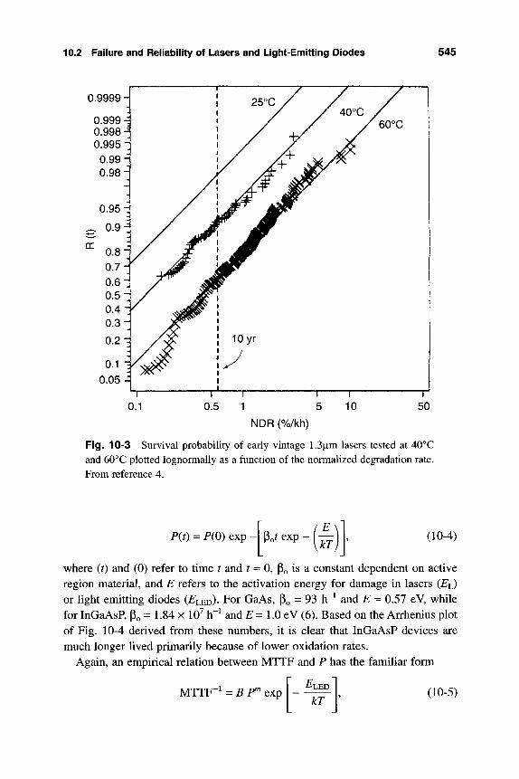
10.2 Failure and Reliability of Lasers and Light-Emitting Diodes 545
0.9999 •
0.999 4 0.998 0.995 i 0.99 i 0.98
0.95-
^ 0.9
^ 0.8' 0.7-0.6 0.5 0.4 0.3
0.2
0.1 1
0.05
0.1 1
0.5 1 5
NDR (%/kh)
1
10 1
50
Fig. 10-3 Survival probability of early vintage 1.3jxm lasers tested at 40°C and 60°C plotted lognormally as a function of the normalized degradation rate. From reference 4.
P(t) = P(0) exp - ^J exp -kT
(10-4)
where (t) and (0) refer to time t and t = 0, % is a. constant dependent on active region material, and E refers to the activation energy for damage in lasers (^L) or light emitting diodes (£'LED)- For GaAs, Po = 93 h~ and E = 0.57 eV, while for InGaAsP, po = 1.84 x lO' h" and £ = 1.0 eV (6). Based on the Arrhenius plot of Fig. 10-4 derived from these numbers, it is clear that InGaAsP devices are much longer lived primarily because of lower oxidation rates.
Again, an empirical relation between MTTF and P has the familiar form
MTTF-^ =BP^ exp kT
(10-5)
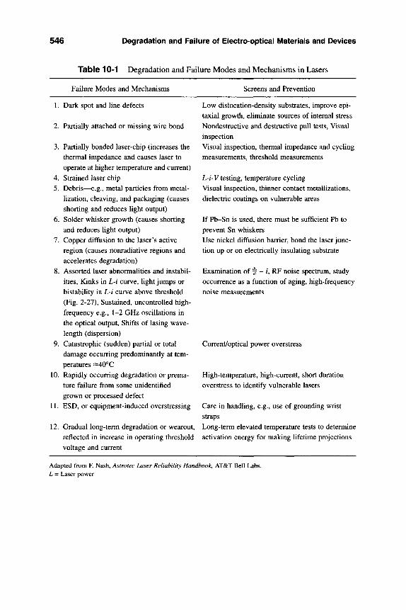
546 Degradation and Failure of Electro-optical Materials and Devices
Table 10-1 Degradation and Failure Modes and Mechanisms in Lasers
Failure Modes and Mechanisms Screens and Prevention
1. Dark spot and line defects
2. Partially attached or missing wire bond
3. Partially bonded laser-chip (increases the thermal impedance and causes laser to operate at higher temperature and current)
4. Strained laser chip 5. Debris—e.g., metal particles from metal-
lization, cleaving, and packaging (causes shorting and reduces light output)
6. Solder whisker growth (causes shorting and reduces light output)
7. Copper diffusion to die laser's active region (causes nonradiative regions and accelerates degradation)
8. Assorted laser abnormalities and instabil-ities. Kinks in L-i curve, light jumps or bistability in L-i curve above threshold (Fig. 2-27), Sustained, uncontrolled high-frequency e.g., 1-2 GHz oscillations in the optical output. Shifts of lasing wave-length (dispersion)
9. Catastrophic (sudden) partial or total damage occurring predominantly at tem-peratures ~40°C
10. Rapidly occurring degradation or prema-ture failure from some unidentified grown or processed defect
11. BSD, or equipment-induced overstressing
12. Gradual long-term degradation or wearout, reflected in increase in operating threshold voltage and current
Low dislocation-density substrates, improve epi-taxial growth, eliminate sources of internal stress Nondestructive and destructive pull tests, Visual inspection Visual inspection, thermal impedance and cycling measurements, threshold measurements
L-/-V testing, temperature cycling Visual inspection, thinner contact metallizations, dielectric coatings on vulnerable areas
If Pb-Sn is used, there must be sufficient Pb to prevent Sn whiskers Use nickel diffusion barrier, bond the laser junc-tion up or on electrically insulating substrate
Examination of ^ - /, RF noise spectrum, study occurrence as a function of aging, high-frequency noise measurements
Current/optical power overstress
High-temperature, high-current, short duration overstress to identify vulnerable lasers
Care in handling, e.g., use of grounding wrist straps Long-term elevated temperature tests to determine activation energy for making lifetime projections
Adapted from F. Nash, Astrotec Laser Reliability Handbook, AT&T Bell Labs. L = Laser power
10.2 Failure and Reliability of Lasers and Light-Emitting Diodes 547
300 200
10-3h
10-4U
0 •«—»
CO c 10-5 o 'to • D CO
U) CD
Q in-6 lo-^h
10 7 L -
Trc) 100 50
n
U\ K V ^ V> o6 v6
— 1 1 r
(InGaAsP) (EL = 1.0eV)
V vN oV\ a ^ \ ^
A v \ \ \ \ \ \
J L_J
1 Z]
•
—
(AIGaAs)
(£L = 0.56 eV) \ J \ 1
\ \
\ \ 1
\
H 1 0 2
-^103
Hio"
CVI
105 I CD
H106
107
10-8
2.0 2.5 3.0 3.5
1000/r(K-l)
Fig. 10-4 Arrhenius plot of failure times for AIGaAs and InGaAsP lasers. From reference 4.
where B and m are constants. Values for ELED range from 0.35 to 0.8 eV (7) and reflect damage mechanisms that similarly afflict lasers. It is to these mechanisms that we now turn.
10.2.3 Microscopic Mechanisms of Laser Damage
Three main semiconductor-laser failure modes have been distinguished: rapid, gradual, and catastrophic degradation. After lasing commenced, early lasers underwent very rapid degradation and failed too soon to be commercially viable. A primary cause of the rapid degradation is the dark-line defect, which was shown to originate from dislocation networks at p-n junctions. Improvement in materials and processes has extended laser life to the point where wearout fail-
548 Degradation and Failure of Electro-optical l\/laterials and Devices
ures are now the primary reliability concern. Indeed, gradual wearout was the failure mode tracked by constant-light testing in Section 10.2.2.1. The cata-strophic-degradation mode stems from damage to the mirror facets.
It is much easier to monitor light or current changes in these failure modes than it is to unravel the microscopic damage processes and expose the culprits responsible for them. Identifying specific failure mechanisms and the defects involved has only been achieved through the use of the transmission electron microscope (TEM).
10.2.3.1 Dark-Spot and Dark-Line Defects A model for the formation of dark-spot defects (DSD) and dark-line defects (DLD) in AlGaAs/GaAs lasers begins with dislocations that originate from the substrate (8). These dislocations nucleate at stacking faults and extend into the epitaxially grown compound semi-conductor films that comprise the active laser region. Known as threading dislo-cations, these crystallographic defects assume the geometry shown in Fig. 10-5 relative to the active (001) plane. Recombination of carriers without desired light emission (nonradiative recombination) as well as photon absorption processes occur preferentially at dislocations where extra electron states or levels exist. In such cases the photon energy is essentially converted into excitation of lattice vibrations (phonons) and manifested as heat. This enhances the motion of vacancy and interstitial point defects to and from associated dislocations, causing the lat-ter to climb and increase in length, even at room temperature. During further aging the dislocation network grows and elongates in a complicated fashion.
Employing electroluminescence (EL) and photoluminescence (PL) tech-niques, DSDs and DLDs are made visible through promotion (or suppression) of electron-level transitions associated with these defects. Such a dark-line defect is shown in Fig. 10-6. At first DSDs emerge and grow where threading dislocations (Fig. 10-5 a, b) intersect the (Oil) plane. By viewing the device normal to the page or along the [110] direction they can be seen. With aging, DLDs appear as schematically suggested by Fig. 10-5c. Lying in the (Oil) plane they grow by climbing along the [100] direction and are known as <100> DLDs. These as well as <110> DLDs were the cause of rapid degradation in early AlGaAs/GaAs lasers and LEDs. The <110> DLDs in these structures originate from dislocation glide on {111} slip planes during plastic deformation. When projected onto {100} planes they appear as a <110> DLD.
Both types of dark-line defects appear in light-emitting diodes as well as lasers composed of InGaAsP/InP materials. Fortunately, DLD damage is not as serious a reliability concern in 1.3 |im and 1.55 |Lim InGaAsP/InPdevices compared to GaAs-based devices. Reasons for this include low DLD dislocation-climb growth rates and a band structure that is less tolerant of nonradiative recombination processes.
10.2 Failure and Reliability of Lasers and Light-Emitting Diodes 549
<001>
Lll
active layer
<110>
4 stripe
r dark spot (small)
dislocation dipole
^ ^ •^ i XJ^
y^^ \ r L*.
^^^JtX vaci
^ x ^
ersjrtiffl
dark spot (large)
<100>
\
dislocation network
<100> DLD growth
(a)
<100> dark line
EL, PL, EBIC
(b)
Fig. 10-5 (a) Mechanisms for dislocation elongation and generation of vacancies and interstitial atoms, (b) Dark spot and dark line defects gener-ated during aging are revealed by electroluminesence (EL), photolumines-ence (PL) and EBIC (see Sect. 11.5.3.2). After P. W. Hutchinson and P S. Dobson, Phil Mag. 32, 745 (1975).
Strategies to eliminate DLDs focus on both the growth stages and postgrowth fabrication steps involved in device manufacture. Employing low-dislocation GaAs (or In?) substrates (e.g., less than 10^/cm^), improved epitaxy, reduction of internal stress, and elimination of oxygen through gettering action by small amounts of Al and Mg have all helped to increase both yield and reliability. Use of the more compliant soft solders for bonding and attachment to thermally matched substrates are postgrowth methods for minimizing DLDs; lower stresses mean fewer dislocations.
550 Degradation and Failure of Electro-optical Materials and Devices
Fjg. 10-6 Dark spot and dark line defects in 1.30 jim laser revealed by photolumines-cence. Courtesy S. N. G. Chu, Lucent Technologies, Bell Laboratories Innovations.
10.2.3.2 Facet Degradation Degradation of the mirror facets is the cause of an important failure mode in semiconductor lasers known as catastrophic optical damage (COD). Initially, the facets are roughly 100°C higher than the cavity temperature, but when catastrophic damage occurs, accelerated heating causes the facet to melt. The basic damage mechanism involves preferential non-radiative recombination of carriers at facets because of the greater presence of surface states and defects there. Local heating reduces both the semiconductor bandgap energy and thermal conductivity, which in turn promotes optical exci-tation of carriers and further laser light absorption. Ultimately, positive feedback occurs at a critical power-output level and leads to thermal runaway, a process modeled in Section 10.3.4.3.
Facet damage is also believed to involve photo-enhanced oxidation of the III-V elements resulting in the formation of stable oxides. Factors like thermody-namic stability and solubilities of the mixed oxides, and the rate of ion transport through them, influence the rate of oxide growth. The mechanism of photoas-sisted oxidation apparently involves the breaking of bonds due to electron-hole generation as a result of irradiation. This facilitates point defect motion through the lattice. Light with energy greater than the semiconductor band-gap energy {E^ is required for such a mechanism. The more intense the light source, the greater the oxidation rate. Under the same light intensity GaAs/AlGaAs oxidizes at a more rapid rate than GaP, InP, InAs, and Ino.47Gao 53As and Ino.72Gao.28 Aso.59Po.41 lattice-matched to InP. Additionally, higher nonradiative recombina-tion velocities are responsible for greater heating and facet degradation suffered in GaAs/AlGaAs relative to quaternary lasers. The enhanced aluminum oxidation at facets explains the trend to Al-free IR laser diodes.
10.2 Failure and Reliability of Lasers and Light-Emitting Diodes 551
Suppression and elimination of facet damage has been achieved by reducing light absorption and protecting the facet from atmospheric attack. Doping the active region with Zn lowers E^ slightly. Thus the energy of the light emitted is reduced, and the facet does not absorb it as readily. To effect the latter, coatings of AI2O3, Si02, and SiN; have been used to limit facet oxidation. In this regard, mirror passivation of GaAs/AlGaAs quantum-well lasers through plasma oxida-tion (9) considerably improves resistance to COD relative to unprotected facets, as seen in Fig. 10-7a. Interestingly, an Arrhenius-like plot describes the relation between the log of laser life (MTTF) and the reciprocal of optical power density (PD). This suggests a linear proportionality between the facet temperature (T) and PD, i.e., T=cxFD. Therefore,
MTTF"^ = V exp ^COD
kT (10-6)
where v is a frequency factor and £'COD is the activation energy for COD. Assuming that c = 130 (K-|xm/mW), values of ECOD = 1-38 eV and v = 720s"^ were extracted. Note that at fixed laser currents, equations 10-3 and 10-6 have the same form.
10.2.3.3 Degradation in 1.3 |xm Clianneied-Substrate Buried Het-erostructure (CSBH) Lasers The comprehensive TEM study by Chu et al, (10) of CSBH lasers is an excellent summary of the interplay among various defect mechanisms and enables a better appreciation of degradation in these devices. Due to enhanced optical confinement in the buried crescent-shaped active stripe (Fig. 10-8, also Fig. 2-29), these InGaAsP/InP lasers have low room-temperature threshold currents, making them suitable for high bit-rate optical-communication applications. To obtain a full picture of the distribution of damage at the crecent tips and sidewalls, it was necessary to obtain sections perpendicular and parallel to the stripe. The resultant TEM images are displayed in the montage of Fig. 10-8. Basically, three types of dislocations are generated inside the active region during gradual degradation.
1. 1/2<100> Sessile loops—^These dislocations are usually generated at the sidewaU interface of the active stripe. Loops grow into the active region by con-tinuous condensation of interstitials on the extra dislocation plane.
2. 1/2<110> Slip Dislocations—Generated by stress in the strained layers of zincblende structures, these dislocations lie in (111) slip planes. Once nucleated, internal plastic and thermal stresses cause them to propagate and multiply, form-ing complex dislocation structures.
3. 1/2<110> Misfit Dislocations—Imaging under perpendicular diffraction conditions reveals that these dislocations are pure edge-type and stem from the bottom heterointerface of the active stripe.
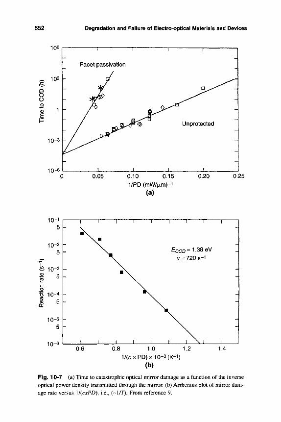
552 Degradation and Failure of Electro-optical Materials and Devices
106
^ iZ
Q O O o 0) E
103
1
10-3 h
10-6
-
r-
k
[-
1
Facet passivation
1
1
1 ^
1
" 1 1
U ^ y ^
Unprotected
1 1
A
A
A
-i
0.05 0.10 0.15 1/PD (mW/fxm)-i
(a)
0.20 0.25
C o CO
l U ' 5
10-2 5
10-3 5
10-4 5
10-5 5
-
-~"
-
1
1
1
1
1 I
• \
1 1__
1 1 1 1 I
^coo =1-38 eV V = 720 s-1
J 1 1 \ 1 L
A
A H
A
H
0.6 0.8 1.0 1.2 1.4
1/(cxPD)x10-3(K-i)
(b)
Fig. 10-7 (a) Time to catastrophic optical mirror damage as a function of the inverse optical power density transmitted through the mirror, (b) Arrhenius plot of mirror dam-age rate versus \l{cxPD), i.e., (-1/T). From reference 9.
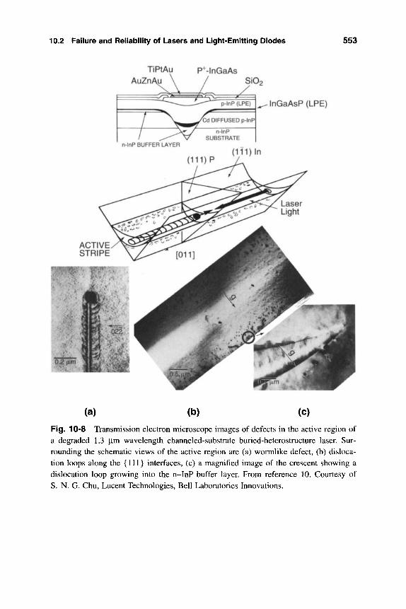
10.2 Failure and Reliability of Lasers and Light-Emitting Diodes 553
TiPtAu P+-lnGaAs AuZnAu \ / Si02
InGaAsP (LPE)
T>W: ff
(a) (b) (c) Fig. 10-8 Transmission electron microscope images of defects in the active region of a degraded 1.3 |xm wavelength channeled-substrate buried-heterostructure laser. Sur-rounding the schematic views of the active region are (a) wormlike defect, (b) disloca-tion loops along the {111} interfaces, (c) a magnified image of the crescent showing a dislocation loop growing into the n-InP buffer layer. From reference 10. Courtesy of S. N. G. Chu, Lucent Technologies, Bell Laboratories Innovations.
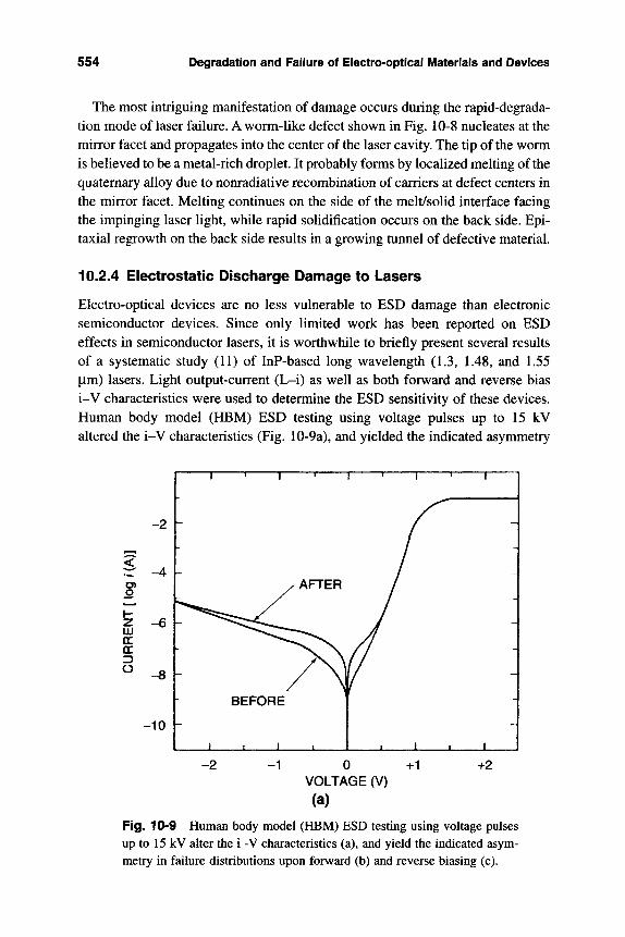
554 Degradation and Failure of Electro-optical Materials and Devices
The most intriguing manifestation of damage occurs during the rapid-degrada-tion mode of laser failure. A worm-like defect shown in Fig. 10-8 nucleates at the mirror facet and propagates into the center of the laser cavity. The tip of the worm is believed to be a metal-rich droplet. It probably forms by localized melting of the quaternary alloy due to nonradiative recombination of carriers at defect centers in the mirror facet. Melting continues on the side of the melt/soUd interface facing the impinging laser light, while rapid solidification occurs on the back side. Epi-taxial regrowth on the back side results in a growing tunnel of defective material.
10.2.4 Electrostatic Discharge Damage to Lasers
Electro-optical devices are no less vulnerable to ESD damage than electronic semiconductor devices. Since only limited work has been reported on ESD effects in semiconductor lasers, it is worthwhile to briefly present several results of a systematic study (11) of InP-based long wavelength (1.3, 1.48, and 1.55 jLim) lasers. Light output-current (L-i) as well as both forward and reverse bias i-V characteristics were used to determine the ESD sensitivity of these devices. Human body model (HBM) ESD testing using voltage pulses up to 15 kV altered the i-V characteristics (Fig. 10-9a), and yielded the indicated asymmetry
-2 h
< r -4 o
tu
3 o
-6 h
-8 h
-10 h
h-
I
h
\-
1 ' 1 T
/AFTER
BEFORE
i t i 1
] 1 1 1 1
/ A
J —j
/ I
i . 1 1
-1 0 +1 VOLTAGE (V)
(a)
+2
Fig. 10-9 Human body model (HBM) ESD testing using voltage pulses up to 15 kV alter the i -V characteristics (a), and yield the indicated asym-metry in failure distributions upon forward (b) and reverse biasing (c).
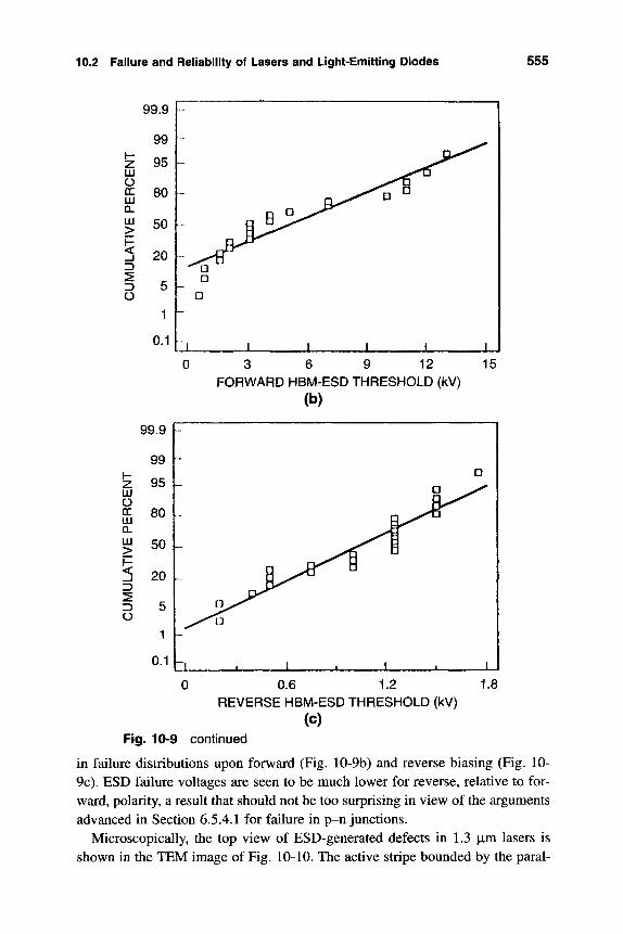
10.2 Failure and Reliability of Lasers and Light-Emitting Diodes 555
LU O oc LU O. LU >
O
LU O OC i l l
LU >
3 O
99.9
99
95
80
50
20
5
1
0.1
-
-
-
._
^00Cr
D D
"I
n B > - ^
-J , _1
^ - - " - " ^
i Jl _.i.J 3 6 9 12
FORWARD HBM-ESD THRESHOLD (kV) (b)
15
99.9
99
95
80
50
20
5
1
0.1
_
-
~
-
-
h.,..
^^y"^ y ^
i t 1 . i
D
1
1 — , . -
a
».I_J 0 0.6 1.2 1.8
REVERSE HBM-ESD THRESHOLD (kV) (C)
Fig. 10-9 continued
in failure distributions upon forward (Fig. 10-9b) and reverse biasing (Fig. 10-9c). BSD failure voltages are seen to be much lower for reverse, relative to for-ward, polarity, a result that should not be too surprising in view of the arguments advanced in Section 6.5.4.1 for failure in p-n junctions.
Microscopically, the top view of ESD-generated defects in 1.3 |im lasers is shown in the TEM image of Fig. 10-10. The active stripe bounded by the paral-
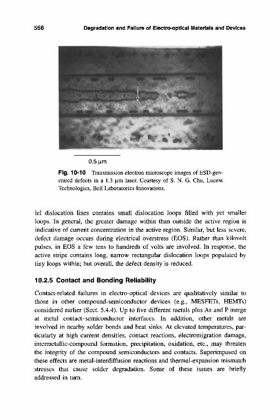
556 Degradation and Failure of Electro-optical Materials and Devices
0.5 jim
Fig. 10-10 Transmission electron microscope images of ESD-gen-erated defects in a 1.3 jxm laser. Courtesy of S. N. G. Chu, Lucent Technologies, Bell Laboratories Innovations.
lei dislocation lines contains small dislocation loops filled with yet smaller loops. In general, the greater damage within than outside the active region is indicative of current concentration in the active region. Similar, but less severe, defect damage occurs during electrical overstress (EOS). Rather than kilovolt pulses, in EOS a few tens to hundreds of volts are involved. In response, the active stripe contains long, narrow rectangular dislocation loops populated by tiny loops within; but overall, the defect density is reduced.
10.2.5 Contact and Bonding Reliability
Contact-related failures in electro-optical devices are qualitatively similar to those in other compound-semiconductor devices (e.g., MESFETs, HEMTs) considered earlier (Sect. 5.4.4). Up to five different metals plus As and P merge at metal contact-semiconductor interfaces. In addition, other metals are involved in nearby solder bonds and heat sinks. At elevated temperatures, par-ticularly at high current densities, contact reactions, electromigration damage, intermetallic-compound formation, precipitation, oxidation, etc., may threaten the integrity of the compound semiconductors and contacts. Superimposed on these effects are metal-interdiffusion reactions and thermal-expansion mismatch stresses that cause solder degradation. Some of these issues are briefly addressed in turn.
10.2 Failure and Reliability of Lasers and Light-Emitting Diodes 557
1. Contacts. Both ohmic and Schottky barrier contacts are used in com-pound-semiconductor electronic devices. However, only the former are used in optical devices, where in addition to ohmic character, contacts must have low electrical and thermal resistivities to suppress the Joule heating that occurs during forward biasing. Common contact metals like Au, Ti, and Pt exhibit large barrier heights (0.8-1 eV) and Schottky behavior when in con-tact with GaAs, InP, and InGaAsP; by alloying, however, the desired ohmic behavior develops. Gold-based contact metallurgies for LEDs have included Au-Zn, Au-Cr, and Ti-Pd-Au, as well as pure Au for p-side contacts. While the Zn-containing contacts degrade at current densities below 12 kA/cm^ with an activation energy of 0.83 eV, the Ti-Pd-Au contacts are relatively immune to damage (7). Accelerated testing causes dark-line defect formation, decreased carrier lifetimes, increased leakage currents, and series resistance, effects that stem in part from interdiffusion of contact metal into the p-n junction. In another study (12) the contact resistance of Ti-Zn-Au on GaAs-based surface LEDs was lower than that of Ti-Pd-Au, accounting for an increase in relia-biUty.
Laser contact metallurgies are also based on Au and display similar damage effects. Reactions between Au and both elements of the underlying InP semi-conductor resemble electrode sinking (see Section 5.4.4.4) and take the form of Ausin compound and AU2P3 cluster formation (13). High current densities also promote electromigration-induced spiking of shallow junctions by filament-like projections of conductive Au3ln.
2. Bonding. Beyond the contacts, metal leads must be connected to the device, which, in turn, is usually attached to a heat sink such as copper or diamond. This raises a host of potential problems associated with solders, attachment materials, and substrates, as discussed by Fukuda (1). Troublesome compound formation sometimes occurs in the attachment between devices and the heat sink. In the case of lasers and LEDs, gold often serves as the cover metal for the heat sink that is bonded to one of the metal electrodes (some-times also gold) via tin or indium-based solder layers. Resulting mass-trans-port mechanisms of the Au-Sn (or Au-In) reactions are schematically depicted in Fig. 10-11. Voids, always a serious reliability concern, are all the more threatening when generated at the electrode-solder interface. In this case Kirkendall voids form due to the unequal rates of rapid grain boundary diffu-sion of Sn into Au, and the slower bulk counterdiffusion of Au into Sn. Con-sequences of interdiffusion are brittle intermetallic-compound formation, lack of adhesion, and loss in heat conduction. As a result, devices operate at higher temperatures, and the effective heat-sink area shrinks due to void for-mation and solder melting. In bootstrap fashion, the hotter laser causes greater
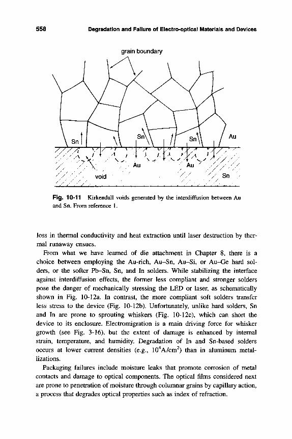
558 Degradation and Failure of Electro-optical Materials and Devices
grain boundary
/ / / /A . / I \ I \ y A
^ . i « / * /
Fig. 10-11 Kirkendall voids generated by the interdiffusion between Au and Sn. From reference 1.
loss in thermal conductivity and heat extraction until laser destruction by ther-mal runaway ensues.
From what we have learned of die attachment in Chapter 8, there is a choice between employing the Au-rich, Au-Sn, Au-Si, or Au-Ge hard sol-ders, or the softer Pb-Sn, Sn, and In solders. While stabilizing the interface against interdiffusion effects, the former less compliant and stronger solders pose the danger of mechanically stressing the LED or laser, as schematically shown in Fig. 10-12a. In contrast, the more compliant soft solders transfer less stress to the device (Fig. 10-12b). Unfortunately, unlike hard solders, Sn and In are prone to sprouting whiskers (Fig. 10-12c), which can short the device to its enclosure. Electromigration is a main driving force for whisker growth (see Fig. 3-16), but the extent of damage is enhanced by internal strain, temperature, and humidity. Degradation of In and Sn-based solders occurs at lower current densities (e.g., lO' A/cm^) than in aluminum metal-lizations.
Packaging failures include moisture leaks that promote corrosion of metal contacts and damage to optical components. The optical films considered next are prone to penetration of moisture through columnar grains by capillary action, a process that degrades optical properties such as index of refraction.
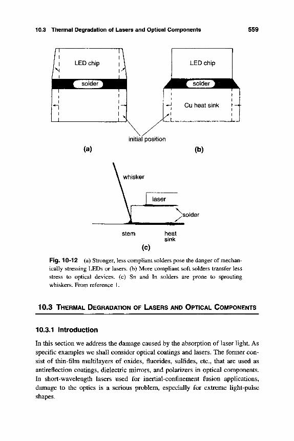
10.3 Thermal Degradation of Lasers and Optical Components 559
initial position
(a) (b)
whisker
laser
\ , solder
stem heat sink
(c) Rg, 10-12 (a) Stronger, less compliant solders pose the danger of mechan-ically stressing LEDs or lasers, (b) More compliant soft solders transfer less stress to optical devices, (c) Sn and In solders are prone to sprouting whiskers. From reference 1.
10-3 THERMAL DEGRADATION OF LASERS AND OPTICAL COMPONENTS
10.3.1 Introduction
In this section we address the damage caused by the absorption of laser light. As specific examples we shall consider optical coatings and lasers. The former con-sist of thin-film multilayers of oxides, fluorides, sulfides, etc., that are used as antireflection coatings, dielectric mirrors, and polarizers in optical components. In short-wavelength lasers used for inertial-confinement fusion applications, damage to the optics is a serious problem, especially for extreme Mght-pulse shapes.
560 Degradation and Failure of Electro-optical Materials and Devices
Radiation incident on a surface with intensity 4 (in units of power density, g., W/cm^
intensity is e.g., W/cm^), is attenuated with distance jc beneath it, such that at any depth the
I(x) = 4 exp [- ajc]. (10-7)
The absorption coefficient a, in reciprocal distance units, is one of the primary properties of concern. Absorption can give rise to beneficial as well as harmful effects; for example, electron-hole pairs are generated during photon absorption in semiconductors, making electro-optical effects possible. However, absorption also necessarily means conversion of radiant energy into potentially damaging heat. Actually, a is derived from the complex index of refraction (N = n - ik) which in turn has real and imaginary components. The former is the real index of refraction (n), while the latter is the index of absorption (k), a quantity related directly to a, i.e., a = 4nk/X, where X is the photon wavelength.
Absorption is usually accompanied by some sort of electronic-excitation process. In optical components (coatings, optical fibers) impurity atoms, ions, and defects are effectively photon absorbers, and every effort is made to remove these because k (or a) is reduced this way. Absorption coefficients in all materi-als are highly dependent on wavelength. Semiconductors, for example, strongly absorb radiation having energies greater than that of the band gap (E^), creating carriers in the process; but they are transparent to photons with energies less than Eg (see Eq. 2-1). In addition, a is a function of temperature, a fact that may pro-mote catastrophic damage to optical devices when heating is uncontrolled (see Section 10.3.4.3).
Although it certainly makes a difference what the absorption mechanism is, under certain circumstances there are broad similarities in the heating effects produced irrespective of material. It is therefore worthwhile to treat first the generic problem of radiation absorption, and later particularize the phenomenon to specific materials and devices.
10.3.2 Thermal Analysis of Heating
In the simplest case we assume a homogeneous material heated by exposure to radiation of intensity /. The fundamental equation for one-dimensional heat con-duction that must be solved to obtain the temperature T(x, t), has the form
r)^T cP'T CO ^rrix, i) = K^r-^(jc, t) + A(x, i), (10-8)
ox ox
where A(JC, t), in units of W/cm^, accounts for the energy absorbed. A physically appropriate expression for this term is A = {\ - R)h{x- X^IQ exp [-ouc], where R is the reflectance from the surface, and the delta function indicates absorption
10.3 Thermal Degradation of Lasers and Optical Components 561
at depth x^ and nowhere else. In this form the equation is generally difficult to solve; when real thin-film coating structures are considered in the next section, one can appreciate just how difficult.
It is instructive to consider absorption of a constant radiant-power density, which in turn produces a constant heat flux at the surface, where the latter is related to the value of A at x^ = 0, i.e., A = (l - R) I^. Under these conditions the thermal history of the irradiated sample can be equivalently described by the heat-conduction theory previously introduced in Section 6.5.3. The boundary value problem that models laser heating in the semi-infinite medium consists of Eq. 6-37 plus the following conditions. Initially,
r ( ; c > 0 , / = 0) = ro. (10-9a)
while the boundary conditions are
T(x = oo^t>0) = To (To is the ambient temperature) (10-9b)
^] =il-R)Io for^>0. (10-9c) dx J x = o
The last condition accounts for the concentration of radiant power in a surface layer, which gives rise to the flux of heat entering the body. When the problem is couched in these terms, the solution is identical to the form of Eq. 6-39, i.e..
^ ^ . 2(1-R)Io {[KtY^^ ( x M j c ^ „ T=T.^——\[-) - P ( - ^ j - i E r f c
2{Y^tf'^ (10-10)
At X = 0 the surface temperature is simply
K \ TC / \7CCpK/
which clearly has the Wunsch-Bell form. As before, damage occurs when some critical temperature level, characteristic of the material, is reached.
Although these equations have a useful pedagogical simplicity, they only begin to address the complexity of actual thermal damage to either thin-film optical coatings or semiconductor lasers. More exact analyses consider hetero-geneous media and material constants that are temperature dependent. Other complications arise from pulsed, as opposed to continuous, laser operation.
10.3.3 Laser-Induced Damage to Optical Coatings
Optical thin films are anything but homogeneous; unlike intrinsic bulk materials, films exhibit nonuniform stoichiometry and property anisotropics (14). These stem from the columnar, polycrystalline-grain structure, in which grains that

562 Degradation and Failure of Electro-optical Materials and Devices
nucleate at the substrate are tiny, but then expand outward Hke inverted cones with further deposition and film growth. Hard-to-remove impurities distributed throughout the structure are sources of absorption, particularly when associated with imperfections and interfaces. More troublesome still are macroscopic inclu-sions or nodules stemming from the bulk-material sources, and the peculiarities of the vapor-deposition method employed. Suspected sources of these nodules include particles "spit" from sputtering targets or electron-beam heated materials that are intolerant of thermal shock.
When nodular heterogeneities such as that shown in Fig. 10-13a are present, it may be assumed that both the absorption coefficients and thermal properties will differ from those of the surrounding matrix. Absorbed laser energy in the nodule vicinity causes a thermal impulse that rapidly heats and locally expands the material. The response has been mathematically modeled by coupling the time-dependent temperature profile evolution with the state of thermal stresses and displacements produced in the matrix (15). As a result of the analysis, the following conclusions were reached:
1. An axisymmetric nodular defect causes significant laser-radiation enhance-ment along its centerline.
2. Both the temperature rise and maximum tensile stress in the nodule depend on the laser pulse-length t; the maximum temperature rise varies as T^^, and the maximum tensile stress is proportional to f^'"^.
3. Nodules that are shallow and have a seed size of about 1 |im will develop the highest temperatures and stresses. Seeds less than 0.25 |im in size are signif-icantly less harmful.
Permanent damage to thin-film optical coatings includes localized pitting from stress-induced nodular ejection (Fig. 10-13b), plasma scalds (Fig. 10-13c), delamination (Fig. 10-13d), and film discoloration. The optical thin films dis-cussed here are an excellent example of how processing defects are the source of later reliability problems. A common measure of the latter is the laser-induced damage-threshold level, a quantity easier to measure than predict. Even a small thermal distortion in a mirror can be fatal in some applications, and therefore efforts should be made to limit the presence of nodular defects of any size.
10.3.4 Thermal Damage to Lasers
In this section we return to laser damage in an attempt to quantitatively model some of the thermally induced failure modes and mechanisms described earlier. Since the classic analysis by Henry et al (16) has served as a standard reference for many later attempts to quantify laser damage, it is worth reviewing some of
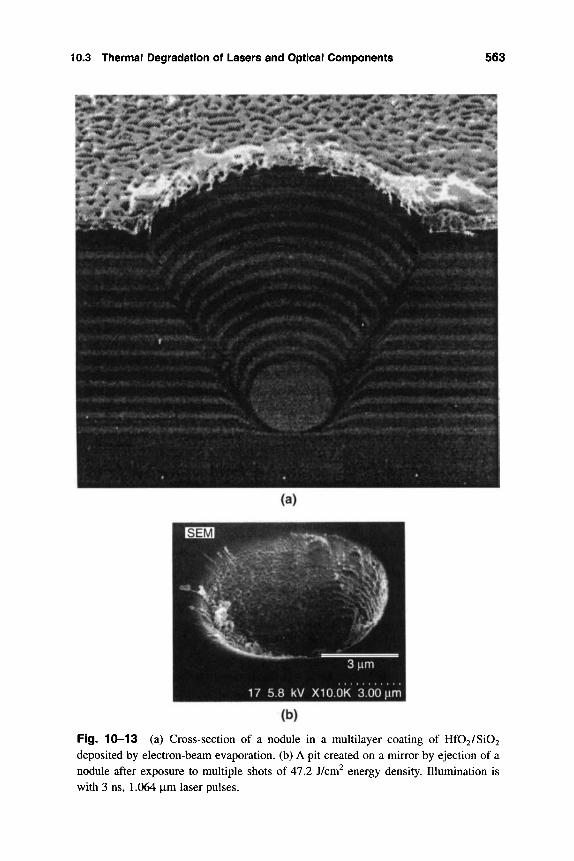
10.3 Thermal Degradation of Lasers and Optical Components 563
Fig. 10-13 (a) Cross-section of a nodule in a multilayer coating of Hf02/Si02 deposited by electron-beam evaporation, (b) A pit created on a mirror by ejection of a nodule after exposure to multiple shots of 47.2 J/cm^ energy density. Illumination is with 3 ns, 1.064 |im laser pulses.
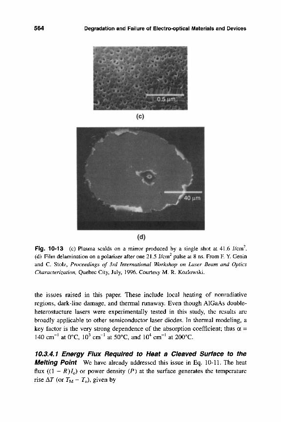
564 Degradation and Failure of Electro-optical Materials and Devices
Fig. 10-13 (c) Plasma scalds on a mirror produced by a single shot at 41.6 J/cm . (d) Film delamination on a polarizer after one 21.5 J/cm^ pulse at 8 ns. From F. Y. Genin and C. Stolz, Proceedings of 3rd International Workshop on Laser Beam and Optics Characterization, Quebec City, July, 1996. Courtesy M. R. Kozlowski.
the issues raised in this paper. These include local heating of nonradiative regions, dark-line damage, and thermal runaway. Even though AlGaAs double-heterostucture lasers were experimentally tested in this study, the results are broadly applicable to other semiconductor laser diodes. In thermal modeling, a key factor is the very strong dependence of the absorption coefficient; thus a = 140 cm"^ at 0°C, 10^ cm"^ at 50°C, and 10^ cm"^ at 200°C.
10.3.4.1 Energy Flux Required to Heat a Cleaved Surface to the Melting Point We have already addressed this issue in Eq. 10-11. The heat flux ((1 - R)Io) or power density {P) at the surface generates the temperature rise M (or TM - T^), given by
10.3 Thermal Degradation of Lasers and Optical Components 565
2 P /KAi/2 A r = ^ ^ — . (10-12)
A meaningful estimate of P entails selecting the right values for K and K, both of which differ in the active and surrounding cladding regions of the laser and are strongly temperature-dependent as well. Taking values at the average tem-perature (900K) between the melting point Tyi and the ambient T^, it is assumed that K = 0.12 W/cm-^ and K = 0.058 cm^/s. Laser pulses of ^ = 18 ns were used to generate melting damage and therefore, by Eq. 10-12, P is calculated to be approximately 4 MW/cm^. When corrected for reflectivity of light at the surface, the optical power flux is still a factor of 2 to 3 lower than that measured to pro-duce damage.
10.3.4.2 Energy Flux Required for Dark-Line Damage In the experi-mental portion of the Henry et al. study, dark lines approximately 0.2 |im in diameter were observed to grow with a velocity of 300 cm/s while absorbing a power of -10 MW/cm^. To reconcile these facts, dark-line defects of dislocation tangles were assumed to behave like molten spheres. This assumption spawned the following thumbnail calculations and estimates:
1. The power to heat the GaAs spheres of radius a (= 0.1|Lim) to the melting point in 18 ns is calculated to be 1.35 x 10"^ W.
2. An additional 7.6 x 10"^ W is needed for melting, assuming the latent heat of GaAs = 3250 J/cml
3. At an average velocity of 300 cm/s the sphere travels a length of 0.054 |im in 18 ns. Additional melting of an equivalent cylinder of this volume requires 3.1 X 10~^W. Summing hives a total power expenditure of 1.46 x 10"^ W.
4. Strong absorption of light occurs inside a waveguide that passes within a ther-mal-diffusion distance (~(K0^^^) beyond the sphere. Therefore, the absorbing cross-section in the active layer is about Aa [a -\- (KtY'^] = 1.6 x 10"^ cm^.
5. The average absorbed flux in the moving sphere is thus calculated to be 1.46 x 10"^ W/1.6 X 10"^ cm^ = 9.1 MW/cml
When accounting for reflection of incident light, the estimated power required for damage is in reasonable quantitative agreement with experiment.
10.3.4.3 Ttiermai Runaway Under conditions of rapid temperature change due to a time-dependent power flux incident at the surface, Eq. 10-12 is too sim-plistic. Instead, heat-conduction theory (17) shows that the temperature rise is given by
1/K\i/2 n P ( t - x ) d T ^T=^-] ^ - ^ . (10-13)
566 Degradation and Failure of Eiectro-optical Materials and Devices
We now recall that P is proportional io{\-R) % exp [-OJC]. However, as already noted, a is temperature (and time) dependent; an exponential relation of the form a (7) = 140 exp [{T - 300)21.4] cm"^ has been suggested by Henry e? al (16) based on experimental data. Folding a (T) into Eq. 10-13 and employing semiconductor carrier dynamics to calculate the effective depth of absorption, the resulting integral equation was solved numerically. The solution is plotted in Fig. 10-14 and indicates that temperature rises parabolically with time at low flux levels. But a two-orders-of-magnitude temperature increase occurs at higher power levels. Importantly, the exact solution follows the "low" curve only to switch to the "high" curve at 18 ns for a power flux of roughly 10 MW/cm^. Thermal runaway is characterized by the substantial temperature increase that occurs within a nanosecond. To complicate matters further, the energy bandgap narrows with increasing temperatures, an effect that is greater in GaAs-based
10,000
1,000
LU CO
LJJ OC
LU CL
LU
100
10
I I I I 1111 - T 1 — I I I I I 11 1 1 — I I I I i U
15MW/cm2 A7(HIGH) _
Ar(LOW)
15MW/cm2
I I M 1 I ^f^\ I ' ' ' • ' ' ' ' I I t I I t I
0.1 1.0 10 TIME(nsec)
100
Fig. 10-14 Temperature rise at a cleaved surface for different incident flux densities. The dashed lines show the temperature rise for constant heating rates of 15 MW/cm . From reference 16.
10.3 Thermal Degradation of Lasers and Optical Components 567
than in quaternary lasers. This further facilitates absorption and the damage feedback loop that accelerates failure.
Analagous thermal-runaway phenomena occur during dielectric breakdown and electrostatic discharge failures. An instructive way to view thermal runaway has been presented by Schatz and Bethea (18), who applied the analysis to facet heating damage in lasers. The approach taken is graphically illustrated in Fig. 10-15. Power dissipated at facets P^ rises steeply with increasing temperature (AT), as shown by the solid lines; by raising output power levels, greater amounts of power are dissipated, i.e., PD(4) > PD(3) > PD(2) > PD(1)- Simulta-neously, heat flow in the device demands a thermal power Px to produce a tem-perature increase (AT); Pj depends on matrix thermal conductivity, dimen-sions of the heated zone, heat-sink geometry, etc., and varies with AT according to the dotted line. Steady-state conditions require that the power
<l 4 h-
0)
o
<D
9-CO
II
1 ^7 PD(4) /
\ ' /
1 1 / ^ 1 / / ^ / / y 1 1 / ^ 1 1 I ^
/ / X 1 / / ** / / /
/ / /
\j/ / 1 y* X
w- ' 1
7 1 \ 7
/Pn(3 ) ' ^ / . ' ' "
/ J--'^ ^1 -*' / 1 ^ / 1
^ y 1
y ' / fb(2) J
^ ^ ^ " ^ PD(1) J
1 —1 1 300 600
Ar(K) 900
<l
4 -1 n o
H 3 CO en CO <D o 0 c CD
o 2 ^
0
1 ^
1200
Fig. 10-15 Dissipated (solid lines) and thermal power (dotted line) as a function of the temperature increase for various levels of output power. The solid points correspond to stable steady-state solutions, while the open point reflects the ther-mal runaway of the unstable solution. From reference 18.
568 Degradation and Failure of Electro-optical Materials and Devices
dissipated be sufficient to generate the heat needed to sustain the temperature. Operating temperatures, or solutions, arise at the intersection of the two curves. The filled circles represent stable solutions because any incremental increase in PD is less than the P j required to maintain the temperature increase; thus, sta-bility occurs when d Pj/d AT > d Pj)/d AT. On the other hand, the open circle solution is unstable; i.e., d P^^ld AT > d P^ldAT. Thermal runaway begins at a power level infinitesimally above PD(3), where there is no mathematical solu-tion. Physically, the power dissipated is too great ever to be conducted away, and Ar spirals upward in an unbounded manner.
10.4 RELIABILITY OF OPTICAL FIBERS
10.4.1 Introduction
In relatively recent years optical fibers have made extraordinarily rapid strides from a laboratory curiosity to a multitude of commercial applications in com-munications, signal processing, and sensors. With information capacities, or bandwidths, thousands of times larger than what is possible in copper wires and circuits, fiber optics have the capability of meeting the burgeoning demands of transmitting voice, data, and video for telephones, computers, and television. Over ten million kilometers of fiber have already been installed in the United States, ninety-five percent of it underground, where the cables are well pro-tected. In the future, however, fiber-in-the-loop leading to businesses and the home will be exposed to harsher environments and increased handling. The dan-ger then exists that the high reliability required of optical fibers will be compro-mised.
Typical optical-communication systems consist of a multilayer fiber with a light source (e.g., laser) at one end that converts the electric-signal message into a series of light pulses. These are transmitted down the fiber, which may be tens of miles long, before the light has to be reamplified at repeater stations. At the other end of the fiber a photodiode detector converts the light back to the origi-nal electrical signal. In high-performance systems these devices operate at 1.55 |im, where maximum light transmission through the fiber occurs. How effi-ciently transmission occurs depends on light attenuation in the fiber. The key for-mula in this regard has already been given in this chapter as Eq. 10-7. Light launched with intensity IQ is attenuated to magnitude / with distance L depend-ing on the absorption coefficient (a) of the fiber; small values of a, or low loss, means fewer costly optical repeaters. It should be appreciated that the reliability
10.4 Reliability of Optical Fibers 569
of the system depends on the individual integrity of the electro-optical devices discussed earlier and the fiber we now consider. Our concern with reliability of fibers will be limited to a decrease in mechanical strength or an increase in opti-cal loss (£). The latter is typically expressed in dBlkm units and defined as £ = - {j) 10 log (f) with L in km. A loss of -0.5 dB/km is a typical value for under-sea fiber.
Optical fiber used for communications consists of an active core of amor-phous Si02 doped with Ge02 in order to raise its index of refraction by about one percent above that of the surrounding Si02 cladding (Fig. 10-16a). This enables light introduced into the core at certain angles to be confined to it with-out escaping into the cladding (Fig. 10-16b). The core and cladding are typically 8.5 and 125 |xm in diameter, respectively; although both are very brittle, they are, paradoxically, required also to be very strong. As we shall see, strength is dramatically reduced by surface damage produced by microcracks and exposure to corrosive environments. Therefore, as soon as the fiber, which is drawn from molten glass, cools sufficiently, it is coated by one or more layers of protective polymer. Some structural and compositional problems and defects that arise in fibers to adversely affect lightguide performance are shown in Fig. 10-17a. Over the last two decades, fiber quality has been systematically improved to the point where defects and impurities have now been largely eliminated. Resulting opti-cal losses due to impurity absorption have been virtually reduced to theoretical limits. In optical-communications systems, fibers are encased in protective cable jackets. Nevertheless, cable-jacket defects and shrinkage may cause the fiber to suffer optical losses due to microbending (Figs. 10-17b, c).
Cladding
Point light ,
uore Polymer source coating
(a) (b) Fig. 10-16 (a) Optical fiber used for communications, (b) Refraction and propagation of light in an optical fiber. Rays 2 and 3 are confined to the fiber. Ray 1, incident on the fiber at too large an angle from the light source, escapes to the cladding. n^{f) and n^c) are refractive indices of the fiber and core.

570 Degradation and Failure of Electro-optical Materials and Devices
ABSORPTION BY
IMPURITY OR OH
CRACK IN SURFACE WILL
ULTIMATELY CAUSE A
FIBER BREAK
MICROBENOING LOSS FROM
SURFACE DISTORTION
LOSSY CUDOINQ
CAUSES LOSS IN
CORE-QUIDED MODES
BUBBLE PENETRATING
THE CORE CAUSES
BROADBAND LOSS
SMALL COMPOSITIONAL
FLUCTUATIONS CAUSE
RAYLEIQH SCATTER LOSS DIAMETER VARIATIONS
CAUSE CONNECTOR LOSS
GLASS DEPOSITION IRREGULARITIES
CAUSE WAVEGUIDE LOSS BY SCATTERING
INDEX PROFILE ERROR CAUSES
MODE DELAY DISTORTION, THUS
PULSE BROADENING
(LOWER BANDWIDTH)
(a)
COATED FIBER CABLE JACKET-
DEFECT
LATERAL FORCE (b)
CABLE JACKET SHRINKAGE
LONGITUDINAL FORCE (C)
Fig. 10-17 (a) Structural and compositional problems within a fiber that can affect lightguide performance. From J. A. Jefferies and R. J. Klaiber, The Western Electric Engineer XXIV (1), 13 (1980). Optical loss in fiber due to microbending caused by the lateral force induced by a cable jacket defect (b), and shrinkage of the cable jacket (c).
10.4 Reliability of Optical Fibers 571
10.4.2 Optical Fiber Strength
All of the issues we shall consider surrounding the strength of optical fibers have been widely addressed in the literature (19-22). The theoretical strength of silica glass based on the cohesive energy of the Si-O bond is estimated to be about 20 GPa, or 3 million psi. Short lengths of currently produced fibers have a strength of about 5.5 GPa (800 ksi) at ambient temperatures and moisture levels; this mone tfian doubles to 13 GPa at liquid nitrogen temperatures (77K). Only steel piano wire, among structural engineering materials, has strengths approaching these magnitudes. Lower strength levels are, however, observed in longer opti-cal fibers. Variability in glass strength has been universally attributed to the pi es-ence of microscopic surface cracks and modeled in terms of the classic Griffith-crack theory for brittle fracture. This model, which was reviewed and applied to the problem of solder fracture in Section 9.5.4, is central to our understanding of the mechanical strength of optical fiber. Appropriately enough, tests on fine glass filaments demonstrated the validity of the theory in the early 1920s. Since Young's modulus (E) for Si02 is 70 GPa and it suffers little plastic deformation, exceptionally large elastic strains (a/E) of 0.08 to 0.17 are possible at the stress (O) levels quoted above.
According to the Griffith analysis, the strength or critical stress Oc required to cause rapid fracture in a fiber containing surface cracks of depth a is given by
< T e - ^ . (10-14)
In this formula i^ic is the critical stress-intensity factor, and for SiOa it has a value of 0.789 MPa-m^^ . The critical stress for a given crack size is also known as the inert strength, a quantity usually defined at room temperature in the absence of time-dependent degradation. For smaller applied stresses (CJ < 0^) ^ subcritical stress intensity factor K{K< ^i^) applies, where
K =<^Ya^'^. (10-15)
In this case no fracture occurs. The constant Y depends on the crack geometry, and if the latter is semicircular, Y = 1.24. In an alternative view of failure, fast fracture occurs when a flaw reaches a critical size {a^) under a given applied stress 0. These connections between tensile strength and crack size are plotted in Fig. 10-18.
Values of Oc for optical fiber depend on the surface crack size dimensions and the test temperature and strain rate, as well as on environmental conditions. Any-one who has tested brittle materials like glass knows that experimental strength values have a wide statistical spread due in part to grip-induced breakage. This
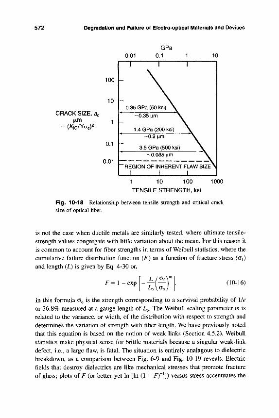
572 Degradation and Failure of Electro-opticai l\/lateriais and Devices
GPa
CRACK SIZE. Be
= (/<IC/Yac)2
100
10
1
0.1
0.01
0.01 0.1
1 1
0.35 GPa (50 ksi) \ -0.35 Mm ' \
1.4 GPa (200 ksi)
1 1C
1 1
-0.2 |im \ 1
3.5 GPa (500 ksi) \ | -0.035 |Lim
^REGION OF INHERENT FLAW S I Z E \ 1 1 -L ._l 1
1 10 100
TENSILE STRENGTH, ksi
1000
Fig. 10-18 Relationship between tensile strength and critical crack size of optical fiber.
is not the case when ductile metals are similarly tested, where ultimate tensile-strength values congregate with little variation about the mean. For this reason it is common to account for fiber strengths in terms of Weibull statistics, where the cumulative failure distribution function (F) as a function of fracture stress (Cf) and length (L) is given by Eq. 4-30 or,
F = I - exp (10-16)
In this formula Go is the strength corresponding to a survival probability of l/e or 36.8% measured at a gauge length of L^. The Weibull scaling parameter m is related to the variance, or width, of the distribution with respect to strength and determines the variation of strength with fiber length. We have previously noted that this equation is based on the notion of weak links (Section 4.5.2). Weibull statistics make physical sense for brittle materials because a singular weak-link defect, i.e., a large flaw, is fatal. The situation is entirely analagous to dielectric breakdown, as a comparison between Fig. 6-9 and Fig. 10-19 reveals. Electric fields that destroy dielectrics are like mechanical stresses that promote fracture of glass; plots of F (or better yet In [In (1 - F)~^]) versus stress accentuates the
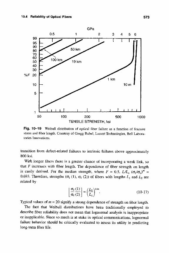
10.4 Reliability of Optical Fibers 573
GPa
100 200 TENSILE STRENGTH, ksi
500 1000
Fig. 10-19 Weibull distribution of optical fiber failure as a function of fracture stress and fiber length. Courtesy of Gregg Bubel, Lucent Technologies, Bell Labora-tories Innovations.
transition from defect-related failures to intrinsic failures above approximately 800 ksi.
With longer fibers there is a greater chance of incorporating a weak link, so that F increases with fiber length. The dependence of fiber strength on length is easily derived. For the median strength, where F = 0.5, L/L^ (Cf/OoT = 0.693. Therefore, strengths (Of (1), Gf (2)) of fibers with lengths Li and L2 are related by
Ofd)
af(2) t) l/m (10-17)
Typical values of m = 20 signify a strong dependence of strength on fiber length. The fact that Weibull distributions have been traditionally employed to
describe fiber reliability does not mean that lognormal analysis is inappropriate or inapplicable. Since so much is at stake in optical communications, lognormal failure behavior should be critically evaluated to assess its utility in predicting long-term fiber life.
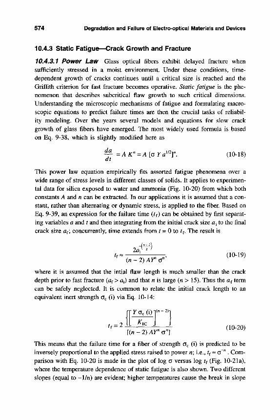
574 Degradation and Failure of Electro-optical Materials and Devices
10.4.3 Static Fatigue—Crack Growth and Fracture
10,4,3,1 Power Law Glass optical fibers exhibit delayed fracture when sufficiently stressed in a moist environment. Under these conditions, time-dependent growth of cracks continues until a critical size is reached and the Griffith criterion for fast fracture becomes operative. Static fatigue is the phe-nomenon that describes subcritical flaw growth to such critical dimensions. Understanding the microscopic mechanisms of fatigue and formulating macro-scopic equations to predict failure times are then the crucial tasks of reliabil-ity modeling. Over the years several models and equations for slow crack growth of glass fibers have emerged. The most widely used formula is based on Eq. 9-38, which is slightly modified here as
— =AK''=A[cY a^'^r. (10-18) dt
This power law equation empirically fits assorted fatigue phenomena over a wide range of stress levels in different classes of solids. It applies to experimen-tal data for silica exposed to water and anmionia (Fig. 10-20) from which both constants A and n can be extracted. In our applications it is assumed that a con-stant, rather than alternating or dynamic stress, is applied to the fiber. Based on Eq. 9-39, an expression for the failure time (ff) can be obtained by first separat-ing variables a and t and then integrating from the initial crack size a^ to the final crack size a^\ concurrently, time extends from / = 0 to tf. The result is
rf« , (10-19) {n-T)Ar<f
where it is assumed that the intial flaw length is much smaller than the crack depth prior to fast fracture {a^ > a^) and that n is large (n > 15). Thus the af term can be safely neglected. It is common to relate the initial crack length to an equivalent inert strength Cc (i) via Eq. 10-14:
• y a c ( i ) i ( ' ' - 2 )
tf=2 K ic
[{n - 2) Ay" a"] (10-20)
This means that the failure time for a fiber of strength o^ (0 is predicted to be inversely proportional to the applied stress raised to power n; i.e., tf ~ a~" . Com-parison with Eq. 10-20 is made in the plot of log a versus log tf (Fig. 10-2la), where the temperature dependence of static fatigue is also shown. Two different slopes (equal to -\ln) are evident; higher temperatures cause the break in slope
10.4 Reliability of Optical Fibers 575
10-8
10-2
10-3 h
(D >
I 10-6 h
10-7 L
A
A '
A Water
• Ammonia
J*
A A
J . X J- J . 0.4 0.6
Stress Intensity K'(MPa-m 1/2) 0.8
Fig. 10-20 Crack velocity as a function of stress intensity for optical fiber exposed to water and ammonia. From T. A. Michalske and B.C. Bunker, J. Appl Phys. 56, 2286 (1984).
(knee) to occur at shorter times. The phenomenon of the knee is treated again in Sect. 10.4.4.1.
10.4,3.2 Exponential Law If crack growth is viewed on a molecular level, it is the chemical reactions which occur between strained bonds in vitreous sil-ica and water that explain environmentally enhanced crack growth. Thus, through analogy to metals, static fatigue is like stress-corrosion cracking. Crack extension ensues when chemical bonds break at a faster rate than they are reformed. The basic degradation reaction is believed to open the silica network so that Si-OH bonds replace Si-0 bonds, i.e..
Si-O-Si + H2O -> Si-OH + HO-Si. (10-21)
Employing concepts from chemical kinetics, the crack growth velocity (v) can simply be written as
da v = - = v.exp
kT (10-22)
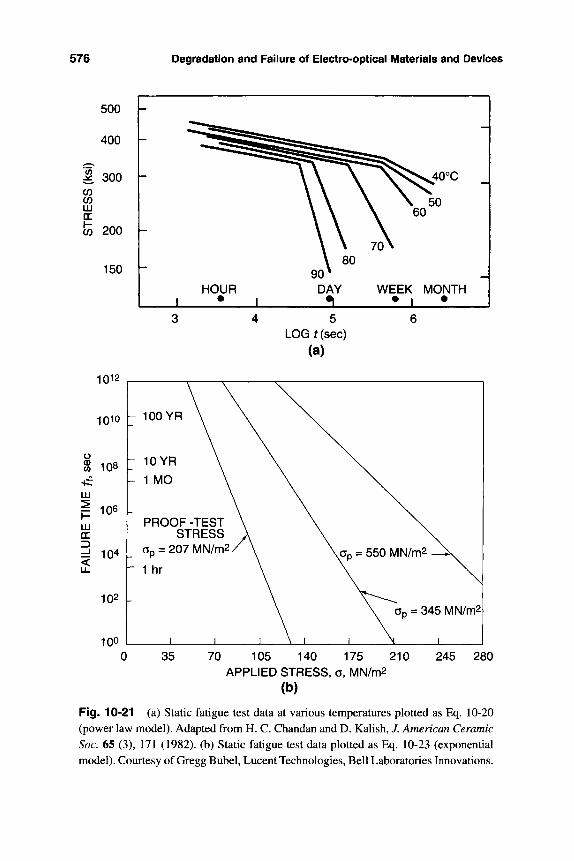
576 Degradation and Failure of Electro-optical Materials and Devices
500 h
400 h
300 h CO CO LU
CO 200 h
150
LOG f (sec)
(a)
1012
1010
§ 108
LU
^ 106 LU DC
d 104 <
102
100
\- 100 YR \ \
h 10YR \ \
P 1 MO \ \
PROOF-TEST \ STRESS \
ap = 207MN/m2/ \
- 1 hr \
1 1 1 \
\ a p = 550 MN/m2 _ i ^
\ Gp = 345 MN/m2
1 1 \ 1 1 35 70 105 140 175 210
APPLIED STRESS, a, MN/m2 (b)
245 280
Fig. 10-21 (a) Static fatigue test data at various temperatures plotted as Eq. 10-20 (power law model). Adapted from H. C. Chandan and D. Kalish, J. American Ceramic Soc. 65 (3), 171 (1982). (b) Static fatigue test data plotted as Eq. 10-23 (exponential model). Courtesy of Gregg Bubel, Lucent Technologies, Bell Laboratories Innovations.
10.4 Reliability of Optical Fibers 577
where E^ is a stress-reduced activation energy for Si-O bond dissociation and Vo is a constant. Specifically, it is assumed that E^ = E^ {\ - K/Kic), where E^ is the activation energy in the absence of stress. Due to the application of a sta-tic stress, E^ is reduced by a factor K/Kic (23). Physically, when K reaches the critical value Kic, fracture proceeds with zero activation energy and is not thermally activated. The form of Eq. 10-22 suggests that the failure time will vary as
tf = to exp a kT
(10-23)
This means that the functional relationship between the failure time and applied stress will show In tf linearly proportional to a, as observed in the static-fatigue data of Fig. 10-21b.
A more rigorous approach to fiber fracture parallels that of power-law kinet-ics of crack growth (Eq. 10-18). Upon substituting the expression for E^, the differential equation describing crack extension that must be solved is of the form
da — = A2 exp at
ni K
ic (10-24)
where A2 = VQ exp [- EJkT], ^2 = EJkT, and where it must be recalled that K is proportional to a time
1/2 Integration between crack lengths a^ and af yields the failure
Z'A2 {[(Z«i ^ + 1) exp Za^^^^] - \{Zal'^ + 1) exp Za^'^Vi, (10-25)
with Z = {EJkT)(Yc/Kic)' An alternative expression derived from Eq. 10-24 that is perhaps more usable has the form
2Kic c^ _1_ Gi ^2
exp an2\ (10-26)
In this equation Gi is the intrinsic glass strength in the absence of fatigue, and Ga is interpreted as the in-service stress. Alternatively, if tf is the design life, Ga can be interpreted as the maximum allowed service stress (24).
Now that expressions for failure times have been developed, one must not be lulled into the comfortable complacency that mechanical reliability of optical fibers is predictable and not a problem. Stress values must be known, and weak points in splices and extra cable twists contribute to them in ways not easily accounted for. In a more dramatic vein, what does one do about shark bites that have damaged undersea cables?
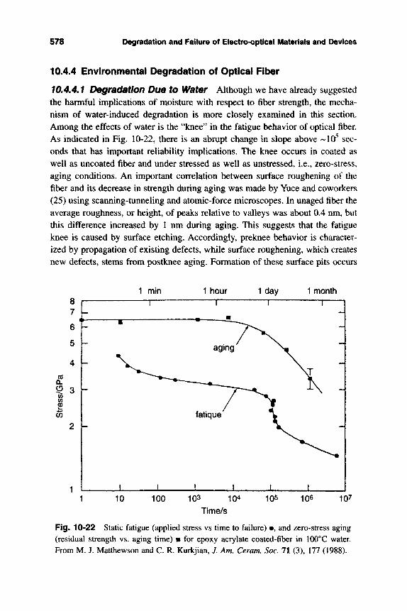
578 Degradation and Failure of EtactroH>pticat Materials and Devices
10.4.4 Envii^nmental Degradation of Optical Fiber
f 0.4,4.1 Degradation Due to Water Although we have already suggested the harmful implications of moisture with respect to fiber strength, the mecha-nism of water-induced degradation is more closely examined in this section. Among the effects of water is the "knee" in the fatigue behavior of optical fiber. As indicated in Fig, 10-22, there is an abrupt change in slope above --10^ sec-onds that has important reliability implications. The knee occurs in coated as well as uncoated fiber and under stressed as well as unstressed, i.e., zero-stress, aging conditions. An important correlation between surface roughening of the fiber and its decrease in strength during aging was made by Yuce and coworkers (25) using scanning-tunneling and atomic-force microscopes. In unaged fiber the average roughness, or height, of peaks relative to valleys was about 0.4 nm, but this difference increased by 1 nm during aging. This suggests that the fatigue knee is caused by surface etching. Accordingly, preknee behavior is character-ized by propagation of existing defects, while surface roughening, which creates new defects, stems from postknee aging. Formation of these surface pits occurs
CO a. o 0) (f) £
CO
103 104 TIme/s
Fig. 10-22 Static fatigue (applied stress vs time to failure) e, and zero-stress aging (residual strength vs. aging time) • for epoxy acrylate coated-fiber in 100°C water. From M. J. Matthewson and C. R. Kurkjian, J. Am, Ceram. Soc. 71 (3), 177 (1988).
10.4 Reliability Of Optli:tmi^« S?9
by a dissolution, or etching, process in which silica is removed, probably in the form of Si(OH)4.
Dissolution is quite distinct from the crack-growth mechanism considered ear-lier, which only requires bond rupture along the crack plane. This etching pmcess differs because material must be removed, and because the surface-mughening reaction is free of the steric hindrance at a crack tip.
10,4*4,2 BWect of HydrogBn Fracture of optical fiber is very much a stress-corrosion phenomenon because cracks extend through chemical reactions that promote a zipper-like severing of Si-0 bonds. In addition to the harmful influ-ence of water, hydrogen is also known to degrade optical fiber. Generated by galvanic corrosion cells present in submerged cables, hydmgen can enter fiber through polymeric coatings. Laboratory simulation studies (26) have shown that com>ding galvanised steel and hydrogen-producing bacteria can substantially raise optical losses. It was concluded that such bacteria found at water crossings near fiber cables, containing metal shields constructed of jute and tar-covered galvanii ed-steel armor wires, could cause harmful light attenuation. Interest-ingly, sulfur-reducing bacteria tend to suppress the effect of the hydrogen-producing bacteria.
Lemaire (27) has extensively investigated the optical degradation due to hydrogen and found that it induces loss absoiption peaks in the range 1.07 to 1.24 |im and a rising loss ''edge" beyond 1,55 |im. TWo useful equations were suggested for estimating time (r)-dependent fiber loss at a hydrogen pressure of 1 atm. The increase in loss at 1.0 jim is
^ = 5 ,6ixlO'rexp 9S.9 kJ/molV kT j
dB/km-h, (10-27)
with corresponding losses at 1.31 jim and 1.55 jim that are 0.7 and 0.55 times the value at l.O |Lim, resp^tively. Similarly, there is a comparable loss due to OH centered at 1.39 jjim that is given by
^ ^ i . 2 x l 0 ^ r e x p dt
/97.3kJ/moiy dBitoi-h. (10-28)
This translates into losses at 1.31 jim and 1.55 iim that are, respectively, only 0.02 and 0.004 times the loss value at 1.39 jLim. In addition, loss increases are also directly proportional to the hydrogen pressure (PH2)- TO produce losses of the magnitudes indicated, molecular hydrogen must diffuse through the coating and cladding and finally enter the light-guiding core region. A preferred value for the diffusion coefficient (Z>) of H2 in silica fibers is given by
580 Degradation and Failure of Electro-optical Materials and Devices
D(H2) = 2.83 X 10"^ exp (- 40.2 kJ/mol/RT) cm^/s. (10-29)
Taking all of these factors into account, it is concluded that after 25 years of service at P^^ = 1 atm, the calculated losses would be intolerable. To prevent hydrogen permeation and mechanical degradation it is common to coat fibers. In addition to polymers, hermetic coatings of carbon and metal films markedly block ingress of hydrogen and minimize optical degradation.
10.4.4.3 Radiation Damage The use of optical fibers in military communi-cations and in radiation environments such as found in reactors, hospitals, nuclear-waste sites, and outer space have raised questions about their long-term reliability. What is of particular concern is the increase in optical loss upon expo-sure to radioactive isotopes and radiation. The same collection of atomic and nuclear particles as well as ionizing radiation (see Section 7.6) that afflicts semi-conductor devices is involved here, and the damage produced is broadly similar. However, in contrast to highly perfect semiconductor lattices, the amorphous glass network contains Schottky and Frenkel defects plus strained bonds and a wide variety of substitutional, interstitial, and multivalent cations as well as non-stoichiometry-induced defects. Electrons and holes created by radiation damage migrate through such a matrix and are either trapped by preexisting or newly created defects. New energy levels are created at these electron-defect centers, enabling absorption of light and a corresponding increase in loss, manifested by a darkening of the fiber.
The extent of radiation-induced fiber degradation depends on a host of vari-ables, including the nature and energy of the radiation, the dose and dose rate, temperature, composition and uniformity of the exposed fiber, and wavelength of operation. Certain of these variables can have potent effects. For example, phosporous-doped fiber exhibits a three-orders-of-magnitude greater loss than silica fiber after exposure to 10^ rads of Co^^ radiation for an hour (19). Time-dependent loss increases for 1.3 |im fiber are shown in Fig. 10-23 for both high and low-dose rate environments.
Optical loss due to radiation has both permanent and transient components. Fortunately, the latter can be diminished by heating, which causes defect annealing, and by exposure to light, which promotes photo-bleaching or recov-ery due to electron-hole recombination. Overall, the effects are such that higher losses are suffered at lower temperatures, assuming equivalent doses. For 1.3 |im fiber irradiated with Co^^ at a dose rate of 213 rad/s, a loss of about 0.4 mdB/km-rad can be expected at 20°C; at -70°C the figure is about 2 mdB/km-rad (19).
In conclusion, a simple mathematical relation that describes the time-dependent change in concentration (Q of the species that promotes loss in irradiated fibers
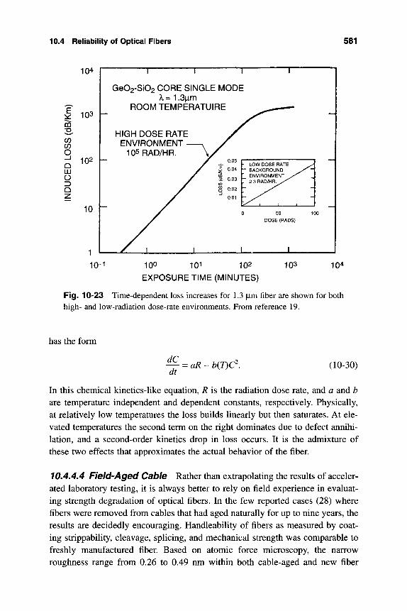
10.4 Reliability of Optical Fibers 581
E
CO CO
O —I Q LU O Q Z
104
103
102
10
T
Ge02-Si02 CORE SINGLE MODE X = 1.3|im
ROOM TEMPERATUIRE
HIGH DOSE RATE ENVIRONMENT
105RAD/HR.
10-1 100 101 102 EXPOSURE TIME (MINUTES)
103 104
Fig. 10-23 Time-dependent loss increases for 1.3 jim fiber are shown for both high- and low-radiation dose-rate environments. From reference 19.
has the form
^ = aR- b{T)C\ at
(10-30)
In this chemical kinetics-like equation, R is the radiation dose rate, and a and b are temperature independent and dependent constants, respectively. Physically, at relatively low temperatures the loss builds linearly but then saturates. At ele-vated temperatures the second term on the right dominates due to defect annihi-lation, and a second-order kinetics drop in loss occurs. It is the admixture of these two effects that approximates the actual behavior of the fiber.
10.4.4.4 Field-Aged Cable Rather than extrapolating the results of acceler-ated laboratory testing, it is always better to rely on field experience in evaluat-ing strength degradation of optical fibers. In the few reported cases (28) where fibers were removed from cables that had aged naturally for up to nine years, the results are decidedly encouraging. Handleability of fibers as measured by coat-ing strippability, cleavage, splicing, and mechanical strength was comparable to freshly manufactured fiber. Based on atomic force microscopy, the narrow roughness range from 0.26 to 0.49 nm within both cable-aged and new fiber
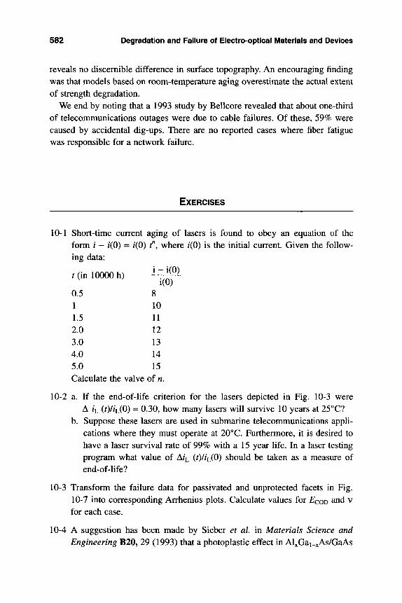
582 Degradation and Failure of Eiectro-opticai iViaterials and Devices
reveals no discernible difference in surface topography. An encouraging finding was that models based on room-temperature aging overestimate the actual extent of strength degradation.
We end by noting that a 1993 study by Bellcore revealed that about one-third of telecommunications outages were due to cable failures. Of these, 59% were caused by accidental dig-ups. There are no reported cases where fiber fatigue was responsible for a network failure.
EXERCISES
10-1 Short-time current aging of lasers is found to obey an equation of the form / - /(O) = /(O) f, where /(O) is the initial current. Given the follow-ing data:
t (in 10000 h)
0.5 1 1.5 2.0 3.0 4.0 5.0
i(0) 8 10 11 12 13 14 15
Calculate the valve of n.
10-2 a. If the end-of-life criterion for the lasers depicted in Fig. 10-3 were A /L (0/^(0) = 0.30, how many lasers will survive 10 years at 25°C?
b. Suppose these lasers are used in submarine telecommunications appli-cations where they must operate at 20°C. Furthermore, it is desired to have a laser survival rate of 99% with a 15 year life. In a laser testing program what value of A/L (0/ 'L(0) should be taken as a measure of end-of-life?
10-3 Transform the failure data for passivated and unprotected facets in Fig. 10-7 into corresponding Arrhenius plots. Calculate values for £"000 i d v for each case.
10-4 A suggestion has been made by Sieber et al. in Materials Science and Engineering B20, 29 (1993) that a photoplastic effect in AlxGai_xAs/GaAs
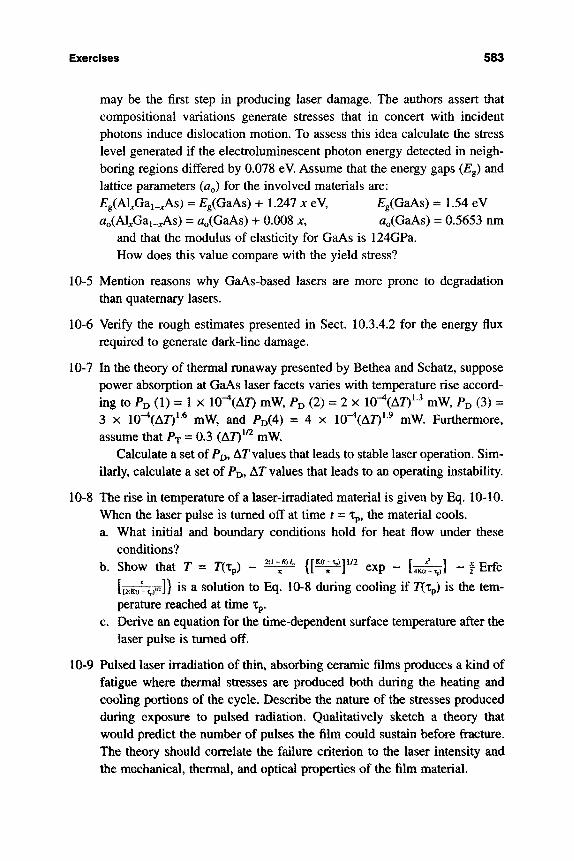
Exercises 583
may be the first step in producing laser damage. The authors assert that compositional variations generate stresses that in concert with incident photons induce dislocation motion. To assess this idea calculate the stress level generated if the electroluminescent photon energy detected in neigh-boring regions differed by 0.078 eV. Assume that the energy gaps (Eg) and lattice parameters (^o) for the involved materials are: £g(Al^Gai_^As) = £g(GaAs) + 1.247 x eV, £g(GaAs) = 1.54 eV ao(Al;,Gai_^As) = ao(GaAs) + 0.008 x, ao(GaAs) = 0.5653 nm
and that the modulus of elasticity for GaAs is 124GPa. How does this value compare with the yield stress?
10-5 Mention reasons why GaAs-based lasers are more prone to degradation than quaternary lasers.
10-6 Verify the rough estimates presented in Sect. 10.3.4.2 for the energy flux required to generate dark-line damage.
10-7 In the theory of thermal runaway presented by Bethea and Schatz, suppose power absorption at GaAs laser facets varies with temperature rise accord-ing to PD (1) = 1 X 10"^(Ar) mW, PD (2) = 2 X lO-^(AJ)^ ^ mW, P^ (3) = 3 X lO^iAT)^^ mW, and Po(4) = 4 x 10"^(AJ)^^ mW. Furthermore, assume that PT = 0-3 (AT)^^ mW.
Calculate a set of P^, AF values that leads to stable laser operation. Sim-ilarly, calculate a set of P^, AT values that leads to an operating instability.
10-8 The rise in temperature of a laser-irradiated material is given by Eq. 10-10. When die laser pulse is turned off at time / = tp, the material cools. a. What initial and boundary conditions hold for heat flow under these
conditions? b. Show that T = nx,) - ^H^li ( [B^]i /2 exp - [ ^ ] - f Erfc
[l2(K(rv^]} is a solution to Eq. 10-8 during cooling if IXXp) is the tem-perature reached at time tp.
c. Derive an equation for the time-dependent surface temperature after the laser pulse is turned off.
10-9 Pulsed laser irradiation of thin, absorbing ceramic films produces a kind of fatigue where thermal stresses are prcduced both during the heating ^ d cooling portions of the cycle. Describe the nature of the stresses produced during exposure to pulsed radiation. Qualitatively sketch a theory that would predict the number of pulses the film could sustain before fracture. The theory should correlate the failure criterion to the laser intensity and the mechanical, thermal, and optical properties of the film material.

584 Degradation and Failure of Electro-opticai i\/laterials and Devices
10-10 Relative to silicon integrated circuits, the manufacturing of semiconduc-tor lasers tends to be less automated and involves more art. There are vastly fewer processing and lithography steps, a simple metallization and contact scheme, and greater variability in the dimensions of device fea-tures. What are the implications of these factors on laser reliability?
10-11 In Griffith-crack theory the static energy surrounding a plate containing a flat crack of size a is W = - 7ca a^/E + 4y a. Stress a acts to open the crack, while surface tension y acts to seal it shut. a. What is the stress required to just cause the crack to open? b. To determine the fracture velocity v, the kinetic energy, Vi kpv^ a^ (o/Ef,
must be accounted for, where p is the density, E is the elastic midulus and A: is a constant. Explain why the kinetic energy has this form.
c. The rate of release of kinetic (strain) energy limits the crack velocity achieved. Show that the value for v that minimizes both the static and kinetic strain energies as well as the surface energy is equal to ( v [ ~ t]}^^^' where «c is the critical crack size.
d. Comment on the difference between v here and da/dt in the text.
10-12 Failure-time data for unstressed optical fiber as a function of temperature gave an Arrhenius plot with an activation energy value of 18 kcal/mol. When the fiber was stressed to 3.44 GPa, the activation energy was found to be 10.7 kcal/mol. a. What is the value for the activation volume, and is it reasonable? b. Suggest a way to obtain a value for Kic from such data.
10-13 From Fig. 10-19 what is the value of m? What is the median strength for 10 km lengths of this fiber?
10-14 Optical fiber exposed to deuterium oxide (D2O) is longer lived relative to similar fiber exposed to H2O at the same strain level. Suggest a possible reason for this. Plot this result as the cumulative failure probability ver-sus log failure time if the ratio of the times to failure for these differently exposed fibers is roughly 2.
10-15 In dynamic fatigue of optical fiber, a phenomenon that parallels that of static fatigue, the fiber strength is dependent on the stress rate, i.e., dc/dt. j_ a. If a = ^ jc da/dt, show that the fiber strength varies as (^ j through
application of the fatigue power law. b. What fiber strength can be expected at a stress rate of 1 ksi/s if the
strength is 800 ksi at a stress rate of 1000 ksi/s.? Assume n = 20.
References 585
10-16 Assume that a fiber withstands a stress of 700 ksi for 1 second. How long would the fiber survive at a stress of 300 ksi if n = 24?
10-17 A bent fiber has a maximum tensile strength, c^^x^ given by c = E r/R, where R is the bend radius of curvature and r is the fiber radius. a. What is the maximum tensile stress for a fiber bent to a radius of 0.75 cm? b. A fiber stressed to this level failed after 1 month. For a 25 year life
what strength fiber would be required? Assume E = 10 GPa and r = 62.5 |Lim.
10-18 Both amorphous polymers and glasses degrade optically due to radiation damage. But only polymers suffer appreciable mechanical deterioration as well. Why? Explain possible reasons why silica fibers do not suffer mechanical damage upon exposure to ionizing radiation.
10-19 Reliability of optical fiber after 25 years implies a loss increase of no more than 0.1 dB/km. What is the maximum hydrogen pressure that can be tolerated such that this level of loss at 1.31 and 1.55 |im is not exceeded during this time at 30°C?
10-20 Suggest a strategy for altering protective coatings in order to inhibit sur-face roughening of optical fibers due to etching.
10-21 With little loss in generality, Eq. 10-30 expresses the radiation-induced time-dependent loss (X) in optical fiber as dL/dt = a'R - bXT)l}, where a' and b' are constants. Obtain a solution for loss as a function of time through separation of variables and direct integration. Assume that ini-tially X = 0.12 dB/km.
Does a log X-log t plot of the solution resemble Fig. 10-22?
REFERENCES
M. Fukuda, Reliability and Degradation of Semiconductor Lasers and LEDs, Artech House, Boston (1991). R. S. Mann and D. K. McElfresh, 33rd Annual Proceedings of the IEEE Reliability Physics Symposium, p. 177 (1995). D. L. Barton, J. Zeller, B. S. Phillips, R-C. Chiu, S. Askar, D.-S. Lee, M. Osinski, and K. J. Malloy, 33rd Annual Proceedings of the IEEE Reliability Physics Symposium, p. 191 (1995).
$SQ DtinMdNilloii 9ii€l Falliim of iK<H;itrcKi|>ticiat Alaitrltlt unci D^viots
4, R R. Nash, Estimi^tmg Devke Retiabitity: Assessmmt of Credibility, Kluwer, Boston (1993),
5. B. Mroziiewic , M, Bugajski, and W, Nakwaski, Physics of Semicmdmtor lasers. North Holland, Amsterdam (1991).
6. S, Yamakoshi, M, Abe, O, Wada, S. Komiya, and X Saknral JEEEI Qum-mm Efectnmics, QE17 Ul (1981),
7, M. Fuknda, IEEE I Ughtwme Tech 6 (10), 1488 (1988), 8. R W. Hutchinson and P. S. Dobson, Fhil Mag. 32, 745 (1975). 9, A, Moser and E, E. Latta, J. Appl Phys, 71 (10), 4848 (1992).
10. S, N. G. Chu, S, Nakahara, M. E, Twigg, L. A. Koszi, E. J. Flynn, A, K, Chin, B. P. Segner, and W, D. Johnston, I Appl Phys. ^ (3), 611 (1988).
IL X Twu, L. S, Cheng, S. N. G. Chu, E R, Nash, K, W, Wang, and P Parayan-thai, i. Appl Pkys. 74 (3), 1510 (1993),
12, C. E. Lindsay, Quality and Reliability Engineering International % 143 (1993).
13, A. Piotrowska, P. Auvray, A. Guivarc'h, G. Pelous, and P. Henoc, J. Appl Ffty5 52, 5112 (1981).
14, M. Ohring, The Materials Science of Thin Films, Academic Press, Boston (1992).
15, R. H, Sawicki, C, C. Shang and T. L, Swatlowski, Laser-Indnced Damage in Optical Materials, SPIE 2428, 333 (1994),
16, C. H, Henry, R M. Petroff, R, A. Logan, and R R, Merritt, 7, Appl Phys. 50 (5) 3721 (1979).
17, H. S, Carslaw and J. C, Jaeger, Conduction of Heat in Solids, 2nd. ed., Oxford, London (1959).
18, R, Schatz and C, G, Bethea, / Appl Phys,, 76, 2509 (1994), 19, S. R. Nagel, SPIE Illy 8 (1986). 20, C. R. Kurkjian and D. Inniss, Optical Engineering 30 (6), 681 (1991), 21, G, M, Bubel and M. J. Matthewson, Optical Engineering 30 (6), 737 (1991). 22, R R Kapron and H, Y. Yuce, Optical Engineering 30 (6), 700 (1991), 23, K, Abe, G, S. Glaesemann, S. T. Gulati and T, A. Hanson, Optical Engi-
neering 30 (6) 728 (1991), 24, M. J. Matthewson, V. V, Rondinella, and C, R, Kurkjian, SPIE 1791, 52
(1992). 25, H. H. Yuce, J. R Varachi, J. R Kilmer, C. R, Kurkjian, and M. J. Matthewson,
OFC'92 Tech, Digest, Post deadline paper PD91, San Diego, CA (1992), 26, G, Schick, K. A. Tellefsen, A. J. Johnson, and C. J. Wieczorek, Optical
Engineering 30 (6) 790 (1991), 27, R J. Lemaire, Optical Engineering 30 (6) 780 (1991), 28, J. L, Smith, A. Dwivedi, and R T, Garvey, International Wire and Cable
Symposium Proceedings, 848 (1995),
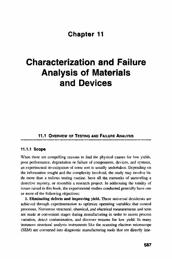
Chapter 11
Characterization and Failure Analysis of IVIaterials
and Devices
11,1 OVERVIEW OF TESTINO AND FAILURE ANALYSIS
11JJ Scopt
When there are compelUng reasons to find the physical causes for low yields, poor j^rformance, degradation or failure of components, devices, and systems, an experimental investigation of some sort is usually undertaken. Depending on the information sought and the complexity involved, the study may involve lit-tle more than a tedious testing routine, have all the earmarks of unraveling a detective mystery, or resemble a research project. In addressing the totality of issues raised in this book, the experimental studies conductedl generally have one or more of the following objectives:
1, Eliminating diefects and improving yi ld* These universal desiderata are achieved through experimentation to optimize operating variables that control processes. Numerous structural, chenucal, and electrical measurements and tests are made at convenient stages during manufacturing in order to assess process variation, detect contamination, and discover reasons for low yield. In many instances structural analysis instruments like the scanning electron microscope (SEM) are converted into diagnostic manufacturing tools that are directly inte-
SS7
588 Characterization and Failure Analysis of Materials and Devices
grated into processing lines to identify defects and maintain feature dimensions. The intent is to eliminate defects at the source.
2. Quality control. After manufacturing is completed, the product normally undergoes a battery of tests to ensure that it meets design goals. Most important are the electrical measurements of voltage, current, light output, etc., specifica-tions that are used to qualify the product.
3. Reliability testing. Assessing the future performance of the product is the purpose of reliability testing. At first there is bum in, a procedure where elevated stress levels of voltage, current, temperature, mechanical loads, etc., are applied to completed manufactured items. The rationale is that if products can withstand the ordeal, they are fit for shipment to customers. In this way infant-mortality failures are weeded out. Some of the wafer-level tests are also performed, e.g., SWEAT, to rapidly assess susceptibility to electromigration damage.
Extensive longer-term reliability testing is conducted to gather data needed to predict failure lifetimes; the TDDB test for dielectrics, discussed in Section 6.3.5, is an example. Irrespective of the component, device, or system involved, the intent is to simulate and accelerate failures such that sufficient data are generated for statistical analysis. Most of the published research in the field and virtually all of the data presented in the book stem from such studies. Routine time-to-failure data as a function of the acceleration factors, though essential, offer little insight into failure mechanisms. To model microscopic failure mechanisms and make more accurate lifetime predictions, it is often necessary to determine material con-stants (e.g., diffusion coefficient, thermal conductivity) and parameters (e.g., acti-vation energies) along the way. Now research is involved, usually necessitating an array of impressive analytical instruments and careful measurement.
4. Failure analysis. When failure occurs in the field, an investigation is nor-mally carried out to determine the cause. The laboratory procedure is known as failure analysis, sometimes termed failure mode analysis (FMA), and generally involves electrical testing as well as structural and chemical characterization. In a four-pronged investigative thrust, the failure mode (e.g., open circuit, leakage current) is first identified, and then iht failure defect (e.g., microcracks, growths) is exposed. Next, the failure mechanism (e.g., electromigration, corrosion) is suggested, and finally the failure cause (e.g., poor design, excessive current den-sity) is proposed so that corrective action can be taken. A collection of failure modes, defects, and mechanisms is presented in Table 11-1.
Note that these four reasons for testing and experimentation are interdepen-dent. Information gained during failure analysis and reliability testing is com-bined, and in turn fed back so that process changes can be made to eliminate product defects in the first place. The tighter the feedback loop, the greater is the probability that failure analysis will be unnecessary.
Table 11-1 Failure Modes, Defects, Mechanisms, and Causes
Failure Mode
Reported Fault Open-circuit (OC)
Short-circuit (SC)
Leakage
Failure Defect
Analysis Missing interconnects Corrosion
Mechanical damage, scratching Open bond
Open metallization
Metallization microcracks Local disruption of interconnects Die cracking Surface contamination
Isolation layer pin holes Hillocks
Local disruption of interconnects
Metal spikes
Metal shorts
Package lead short
Surface contamination
Failure Mechanism and Cause
Interpretation Mask errors 1. 2.
Moisture (internal gas; poor seal) Contaminants + moisture
Poor processing/handling 1. 2. 3. 4. 5. 1. 2.
3. 4.
Pad contaminant Bonding overpressure Package stress Al/Au intermetallic formation Fatigue failure Electromigration Processing defects, e.g., step coverage, litho-graphy Corrosion Wrong passivation composition
Stress, migration in as-deposited metallization 1. 2.
Electrical overstress Electrostatic discharge
Thermal/mechanical stress 1. 2.
Contaminant between tracks Metal migration/dendrites
Direct SC 1. 2. 1. 2. 1. 2. 3. 4. 1. 2. 3. 4. 5. 1. 2. 3. 1. 2.
Electromigration SC Whisker growth in double layer metal Electrical overstress Electrostatic discharge Enhanced diffusion along dislocations Poor contact alloying Overstress giving spiking Electrothermal overstress Poor bond placement Metallization definition defects Bond wire to substrate short Electromigration Stress-induced whisker growth Whisker growth—tin plating Whisker growth due to corrosion Whisker growth—frit seal Surface leakage Ionic contamination at oxide/silicon interface
High temperature
failure
Poor junction delineation
Oxide breakdown
Hot spots
Metal spikes
Defective die-attach
Processing defects
1. Voltage overstress
2. Oxide defects
1. Power dissipation at metallization defects
2. Current concentration at crystallographic
defects
Metal diffusion along crystal defects
Thermal overstress
From B. P. Richards and P. K. Footner, Microelectronics Journal 15 (1), 5 (1984) and The Role of Microscopy in Semiconductor Failure Analysis, Oxford University Press, Oxford (1992).
589
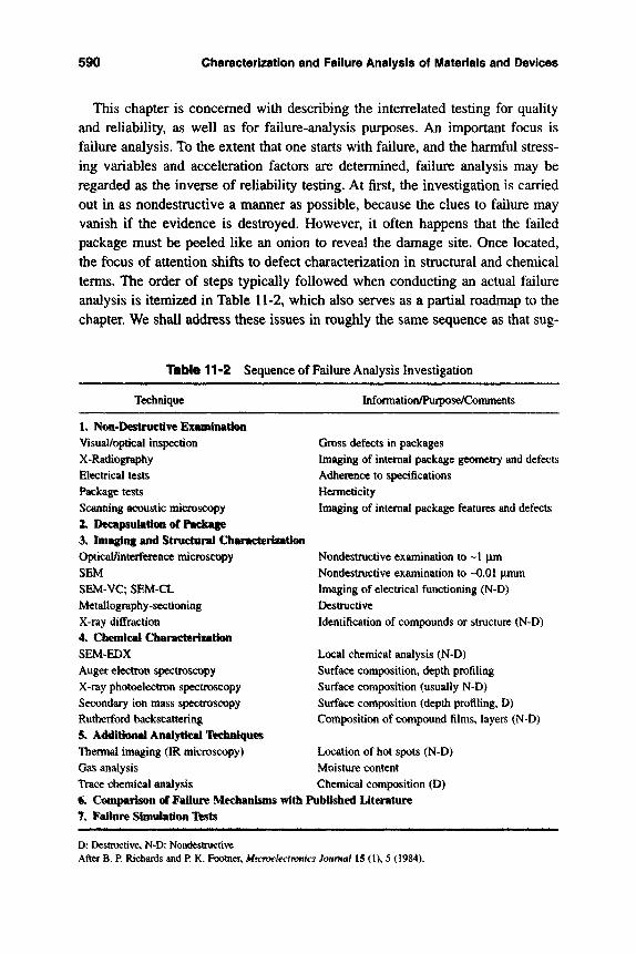
590 Characterization and Faiiure Anaiysis of l\/lateriais and Devices
This chapter is concerned with describing the interrelated testing for quality and reliability, as well as for failure-analysis purposes. An important focus is failure analysis. To the extent that one starts with failure, and the harmful stress-ing variables and acceleration factors are determined, failure analysis may be regarded as the inverse of reliability testing. At first, the investigation is carried out in as nondestructive a manner as possible, because the clues to failure may vanish if the evidence is destroyed. However, it often happens that the failed package must be peeled like an onion to reveal the damage site. Once located, the focus of attention shifts to defect characterization in structural and chemical temis. The order of steps typically followed when conducting an actual failure analysis is itemized in Table 11-2, which also serves as a partial roadmap to the chapter. We shall address these issues in roughly the same sequence as that sug-
Table 11-2 Sequence of Failure Analysis Investigation
Technique Information/Purpose/Comments
1. Non-Destructive Examination Visual/opticai inspection X-Radiography Electrical tests Package tests Sciuining acoustic microscopy 2. Decapsulation of Piickage 3. Imaging and Structural Characterization Optical/interference microscopy SEM SEM VC; SEM-CL Metallography-sectioning X-ray diffraction 4. Chemical Characterization SEM'EDX Auger electron spectroscopy X-ray photoelectron spectroscopy Secondary ion mass spectroscopy Rutherford backscattering 5* A4dlti<mal Analytical techniques Thermal imaging (IR microscopy) Gas analysis Trace chemical analysis <k Con^r ib»n of Failure Mechanisms viitk 7. Failure Simulation l\»sts
Gross defects in packages Imaging of internal package geometry and defects Adherence to specifications Hermeticity Imaging of internal package features and defects
Nondestructive examination to ~1 |xm Nondestructive examination to -0.01 ^mm Imaging of electrical functioning (N-D) Destructive Identification of compounds or structure (N-D)
Local chemical analysis (N-D) Surface composition, depth profiling Surface composition (usually N-D) Surface composition (depth profiling, D) Composition of compound films, layers (N-D)
Location of hot spots (N-D) Moisture content Chemical composition (D)
PubHshed Literature
D Destitictive, N-Di Nondesmictive After Bv P. Richaixls and P K. Fotymer, Mitmekctrmics Journal 15 (1), 5 (1984).
11.1 Overview of Testing and Faiiure Anaiysis 591
gested in the table. In addition, this table catalogs a great many of the techniques that will be discussed.
To illustrate the methodology, case histories of defects or failures will be interspersed throughout.
11.1.2 Characterization Tools and IMethods
Although defects and failure in electronic materials and devices is our concern and these are usually exposed after electrical testing or probing of circuits, there will, paradoxically, be virtually no discussion of electrical testing. This subject is simply well beyond the scope of this book. We may, however, distinguish elec-trical characterization on the chip and individual device levels. For example, the magnitude and time dependence of power supply current (IDDq) drawn by a CMOS circuit can identify devices with excessive leakage and indirectly detect defects (1). In particular, such IDDq testing is well suited to revealing BSD, EOS, and latchup failures and detecting gate oxide and interlayer shorts. Further identification of faulty devices involves generating a datalog profile with auto-mated test equipment. Often these indirect measurements reveal latent electrical open defects, such as conductor line narrowing, notches, and cracks. Electrical testing at the bench then tracks the subsequent destructive unpeeling and char-acterization of the chip. This means curve-tracer analysis relative to a bus pin (usually ground) and determination of dc and ac characteristics. Comparison with the behavior of good devices helps to identify the failure mode.
In keeping with the materials slant of the book, the major focus of attention will be on imaging individual device surface and subsurface features as well as determining local chemical compositions. Analysis on the chip level will be emphasized, but many applications to packaging will be included.
Many of the characterization tools and methods used to improve the quality of electronic products and expose their failure modes and mechanisms are the same as those employed in varied scientific investigations spanning all disciplines. These instruments all function by probing the surface of the specimen with either an input photon, electron, or ion beam, and detecting a signal composed of some combination of output photons, electrons, or ions. Interpreting the inten-sity and spectral response of this output signal is the key to understanding the phenomenon under investigation. Even though there is a broad and accessible literature describing the underlying physics of many of these techniques and the information they convey (2-5), a brief review of these issues will prove instruc-tive. However, space constraints will mean an emphasis primarily on the special features that make these tools and techniques unique in analyzing failure of elec-tronic products.
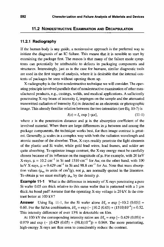
592 Characterization and Failure Analysis of l\/iaterials and Devices
11.2 NONDESTRUCTIVE EXAMINATION AND DECAPSULATION
11.2.1 Radiography
If the human body is any guide, a noninvasive approach is the preferred way to initiate the diagnosis of an IC failure. This means that it is sensible to start by examining the package first. The reason is that many of the failure mode symp-toms can potentially be attributable to defects in packaging components and structures. Interestingly, just as is the case for humans, similar diagnostic tools are used in the first stages of analysis, where it is desirable that the internal con-tents of packages be seen without opening them up.
X-radiography is the first nondestructive technique we will consider. The oper-ating principle involved parallels that of nondestructive examination of other man-ufactured products, e.g., castings, welds, and medical applications. A sufficiently penetrating X-ray beam of intensity 4 impinges on the sample and the attenuated transmitted-radiation of intensity I(x) is detected as an electronic or photographic image. This already familiar relation between the two intensities (see Eq. 10-7) is
/(jc) = /oexp[-M^], (11-1)
where x is the penetration distance and |i is the absorption coefficient of the involved material. When there are large differences in |i between and among the package components, the technique works best, for then image contrast is great-est. Generally, |i scales in a complex way with both the radiation wavelength and atomic number of the absorber. Thus, X-rays readily penetrate the light elements of the plastic and Si wafer, while gold lead wires, lead frames, and solder are quite absorbing. To optimize image contrast, the X-ray energy must be carefully chosen because of its influence on the magnitude of |Li. For example, with 20 keV X-rays, i = 10.2 cm~ in Si and 1510 cm~ for Au; on the other hand, with 100 keV X-rays, |Li = 0.429 cm~ in Si and 98.8 cm"^ for Au. Note that mass absorp-tion values (|Lim in units of cmVg), not |Li, are normally quoted in the literature. To obtain |i we must multiply |im by the density p.
Example 11-1 What is the difference in intensity of X-rays penetrating a pure Si wafer 0.05 cm thick relative to this same wafer that is patterned with a 1 |im thick Au bond pad? Assume that the operating X-ray voltage is 20 kV. Is the con-trast better at 100 kV?
Answer Using Eq. 11-1, for the Si wafer alone I/I^ = exp [-10.2 (0.05)] = 0.60. For the Si/Au combination, I/I^ = exp (- [10.2 (0.05) + (1510)10"^] = 0.52. This intensity difference of over 13% is detectable on film.
At 100 kV the corresponding intensity ratios are I/I^ = exp [-• 0.429 (0.05)] = 0.979 and exp (- [0.429 (0.05) -H (98.8)10"^]) = 0.969. The more penetrating, high-energy X-rays are thus seen to considerably reduce the contrast.
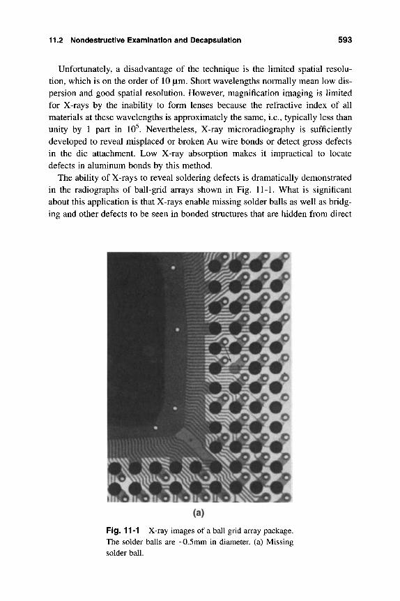
11.2 Nondestructive Examination and Decapsulation 593
Unfortunately, a disadvantage of the technique is the Umited spatial resolu-tion, which is on the order of 10 |im. Short wavelengths normally mean low dis-persion and good spatial resolution. However, magnification imaging is limited for X-rays by the inability to form lenses because the refractive index of all materials at these wavelengths is approximately the same, i.e., typically less than unity by 1 part in 10 . Nevertheless, X-ray microradiography is sufficiently developed to reveal misplaced or broken Au wire bonds or detect gross defects in the die attachment. Low X-ray absorption makes it impractical to locate defects in aluminum bonds by this method.
The ability of X-rays to reveal soldering defects is dramatically demonstrated in the radiographs of ball-grid arrays shown in Fig. 11-1. What is significant about this application is that X-rays enable missing solder balls as well as bridg-ing and other defects to be seen in bonded structures that are hidden from direct
(a)
Fig. 11-1 X-ray images of a ball grid array package. The solder balls are ~0.5mm in diameter, (a) Missing solder ball.
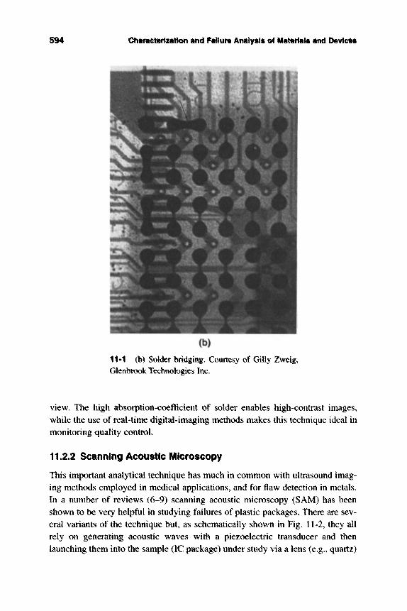
Sd4 Ch&m&miimWm^ m4 nMure Antlytit f MattHnls m4 ^^mkm
11*1 (b) Solder bridging. Courtesy of Gilly Zweig, Glenbtx)ok Technologies Inc.
view. The high absorption-coefficient of solder enables high-contrast images» while the use of real-time digital-imaging methods makes this technique ideal in monitoring quality control.
11.2.2 Scanning Acoustic Microscopy
This important analytical technique has much in common with ultrasound imag-ing methods employed in medical applications, and for flaw detection in metals. In a number of reviews (6-9) scanning acoustic microscopy (SAM) has been shown to be very helpful in studying failures of plastic packages. There are sev-eral variants of the technique but, as schematically shown in Fig. U-2, they all rely on generating acoustic waves with a piezoelectric transducer and then launching them into the sample (IC package) under study via a lens (e.g., quartz)
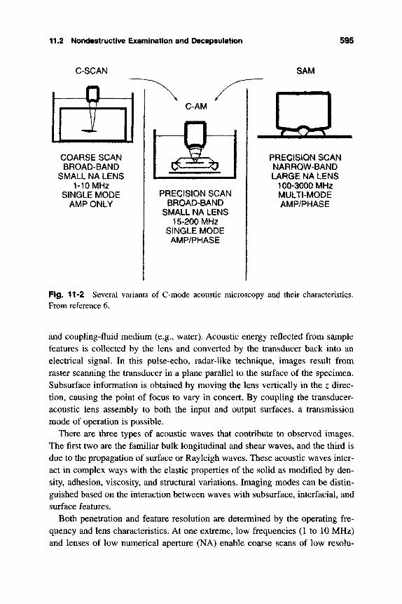
11.2 Nondestructive Examination and Decapsulation 595
C-SCAN SAM
m COARSE SCAN BROAD-BAND
SMALL NA LENS 1-10 MHz
SINGLE MODE AMP ONLY
C-AM
PRECISION SCAN BROAD-BAND
SMALL NA LENS 15-200 MHz
SINGLE MODE AMP/PHASE
TT^T^
PRECISION SCAN NARROW-BAND URGE NA LENS
100-3000 MHz MULTI-MODE AMP/PHASE
Fig, 11-2 Several variants of C-mode acoustic microscopy and their characteristics. From reference 6.
and coupling-fluid medium (e.g., water). Acoustic energy reflected from sample features is collected by the lens and converted by the transducer back into an electrical signal. In this pulse-echo, radar-like technique, images result from raster scanning the transducer in a plane parallel to the surface of the specimen. Subsurface information is obtained by moving the lens vertically in the z direc-tion, causing the point of focus to vary in concert. By coupling the transducer-acoustic lens assembly to both the input and output surfaces, a transmission mode of operation is possible.
There are three types of acoustic waves that contribute to observed images. The first two are the familiar bulk longitudinal and shear waves, and the third is due to the propagation of surface or Rayleigh waves. These acoustic waves inter-act in complex ways with the elastic properties of the solid as modified by den-sity, adhesion, viscosity, and structural variations. Imaging modes can be distin-guished based on the interaction between waves with subsurface, interfacial, and surface features.
Both penetration and feature resolution are determined by the operating fre-quency and lens characteristics. At one extreme, low frequencies (1 to 10 MHz) and lenses of low numerical aperture (NA) enable coarse scans of low resolu-
596 Characterization and Failure Analysis of l\/laterials and Devices
tion, but great depths of imaging (several mm). This is the regime of medical ultrasound and nondestructive testing (NDT). In this so-called C-SCAN mode of operation, detection of cracks in encapsulated ICs and ceramics is possible. At the other extreme, of high frequency (100-2000 MHz) and large NA lenses, the spatial resolution improves to about 1 |xm with a focal depth of a few microme-ters. Imaging depends on the interaction between Rayleigh waves and surface features. In this SAM mode, defects in silicon wafers, film adhesion and delam-ination problems, and metallization structures in ICs can be revealed. Electrostatic-discharge damage to ICs is often more sensitively detected with SAM methods than with optical microscopy. Nevertheless, interpretation of high-frequency images is complicated by the fact that contrast depends on both material and topographical differences that are not easy to separate.
A hybrid of the two established reflection acoustic techniques known as C-AM operates in the range of 15-200 MHz and strikes a good compromise between lateral and depth resolution. Among the package defects that can be analyzed with C-AM are popcorn and radiating cracks, voids in the molding compound, die-attach separation and voiding, wirebond pull-out, and leadframe delamination. This technique is particularly suited to distinguishing between bonded and delaminated interfaces. For example. Fig. 11-3 shows image differ-ences between delaminated areas as well as regions of good adhesion.
In interpreting acoustic imaging a few basic physical principles should be borne in mind. Reflection of sound from layered media of differing densities is similar to the reflection of light from layered optical films of differing refractive indices. The quantity analogous to the real index of refraction is the acoustic impedance (Z), which for longitudinal waves is defined by the product of the speed of sound (m/s) in the medium and its density (kg/m^). Acoustic impedance units are in kg/m^-s or Rayl, and for silicon Z = 20 x 10^ Rayl. Now consider an acoustic wave incident normal to the interface between two media 1 and 2 as shown in Fig. 11-4. Of the acoustic energy incident (EQ), the fractions reflected (ER) and transmitted (Ej) are given given by
E^ = {^^] (11-2) Z2 + Z1
and
4Z2Z1 ET = ^—^. (11-3)
^ (Z2 + Zi)^ ^ ^ Note that ER + Ex = 1. Identical formulas hold for nonabsorbing optical thin films on a transparent substrate. Acoustic wave amplitudes are also dependent on Z. For the geometry indicated, the reflected wave amplitude (AR) is
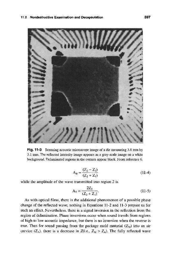
11.2 Nondestructive Examination and Decapsulation 597
\'^yymin Fig. 11-3 Scanning acoustic microscope image of a die measuring 3.6 mm by 3.1 mm. The reflected intensity image appears as a gray-scale image on a white background. Delaminated regions in the comers appear black. From reference 6.
AR = (Z2 - Zi)
(11-4) (Z2 + Z1)
while the amplitude of the wave transmitted into region 2 is
2Z2 AT = - -——-> (11-5)
(Z2 + Z1)
As with optical films, there is the additional phenomenon of a possible phase change of the reflected wave; nothing in Equations 11-2 and 11-3 prepare us for such an effect. Nevertheless, there is a signal inversion in the reflection from the region of delamination. Phase inversions occur when sound travels from regions of high to low acoustic impedance, but there is no inversion when the reverse is true. Thus for sound passing from the package mold material (ZM) into an air crevice (ZA), there is a decrease in Z(i.e., ZM > Zp), The fully reflected wave
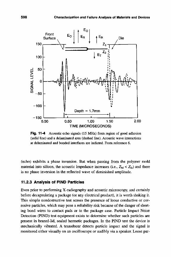
598 Characterization and Failure Analysis of Materials and Devices
Front Surface
150
100
LU > LU
$2 CO
-100 h
-150 0.00 0.50 1.00 1.50
TIME (MICROSECONDS) 2.00
Fig. 11-4 Acoustic echo signals (15 MHz) from region of good adhesion (solid line) and a delaminated area (dashed line). Acoustic wave interactions at delaminated and bonded interfaces are indicted. From reference 6.
(echo) exhibits a phase inversion. But when passing from the polymer mold material into silicon, the acoustic impedance increases (i.e., ZM < Zsi) and there is no phase inversion in the reflected wave of diminished amplitude.
11.2.3 Analysis of FIND Particles
Even prior to performing X-radiography and acoustic microscopy, and certainly before decapsulating a package (or any electrical product), it is worth shaking it. This simple nondestructive test senses the presence of loose conductive or cor-rosive particles, which may pose a reliability risk because of the danger of short-ing bond wires to contact pads or to the package case. Particle Impact Noise Detection (FIND) test equipment exists to determine whether such particles are present in brazed-lid, sealed hermetic packages. In the FIND test the device is mechanically vibrated. A transducer detects particle impact and the signal is monitored either visually on an oscilloscope or audibly via a speaker. Loose par-
11.2 Nondestructive Examination and Decapsulation 599
tides can often be captured for further study by meticulously grinding open a comer of the package, placing tape over the hole and shaking until the noise stops.
11.2.4 Decapsulation
If preliminary nondestructive inspection suggests that analysis at the chip level is required, then decapsulation of the package is required. Prior X-ray or acoustic imaging may be necessary to ascertain the orientation and dimensions of the package contents. This will set guidelines for how much mechanical grinding can be tolerated. Decapsulation, or depackaging, poses different chal-lenges depending on whether the packages have a cavity, e.g., ceramic dual-in-line (CERDIP), or are molded, e.g., plastic dual-in-line package (DIP). For the former, tools like small vice grips, miniature diamond-cutting and grinding wheels, saws, and polishing equipment are employed.
In the molded thermoplastic or thermosetting (epoxies) packages moisture is first removed by baking at low temperature. Now the plastic package is ready for decapsulation. For both thermoplastic or thermosetting molding compounds, a solvent is needed to soften and dissolve the polymer. In the process, plastic par-ticles sometimes break into little pieces that may damage delicate semiconduc-tor component features. Decapsulation is far easier in thermoplastics because many organic solvents exist. For these materials the dissolution process involves a solvation step in which surface absorption of solvent molecules causes the polymer to swell, followed by diffusion of decomposed thermoplastic molecules through the solvent.
The more conmion thermosetting-polymer packaging materials require more powerful inorganic reagents such as concentrated and fuming sulfuric and nitric acids, as well as chromic acid and proprietary commercial formulations (10). It is usually necessary to protect the easily corrodible metal leads, solders, lead frames, and even chip contact pads and metallizations during exposure to such acids. The typical chemical decapsulation station is outfitted with the appropri-ate handling fixtures and tools (tweezers), solvent containers (acid percolator, beakers, eyedroppers) and methods to heat the solutions controUably. Plasmas have also been used to decapsulate chips, but the advantage of etching selectiv-ity is generally offset by the long times required. Aggressive decapsulation methods sometimes raise doubts as to the interpretation of failure. For example, did cracking of the oxide or nitride coating cause the failure, or did the coating crack during decapsulation?
Following depackaging, the remaining chip and supports are ultrasonically cleaned, rinsed, and examined optically. If chip-level features must be revealed.
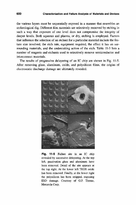
600 Characterization and Failure Analysis of i\/[ateriais and Devices
the various layers must be sequentially exposed in a manner that resembles an archeological dig. Different film materials are selectively removed by etching in such a way that exposure of one level does not compromise the integrity of deeper levels. Both aqueous and plasma, or dry, etching is employed. Factors that influence the selection of an etchant for a particular material include the fea-ture size involved, the etch rate, equipment required, the effect it has on sur-rounding materials, and the undercutting action of the etch. Table 11-3 lists a number of reagents and etchants used to selectively remove semiconductor and interconnect materials.
The results of progressive delayering of an IC chip are shown in Fig. 11-5. After removing glass, aluminum, oxide, and polysilicon films, the origins of electrostatic discharge damage are ultimately revealed.
Fig. 11-5 Failure site in an IC chip revealed by successive delayering. At the top left, passivation glass and aluminum have been removed. Detail of the site appears at the top right. At the lower left TEOS oxide has been removed. Finally, at the lower right the polysilicon has been stripped, exposing BSD damage. Courtesy of G.R Thome, Motorola Corp.
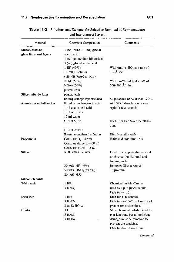
11.2 Nondestructive Examination and Decapsulation 601
Table 11-3
Material
Solutions and Etchants for Selective Removal of Semiconductor
and Interconnect Layers
Chemical Composition Comments
Silicon dioxide glass films and layers
Silicon nitride films
Aluminum metallization
Polysilicon
Silicon
1 (wt)NH4Cl:l (wt) glacial acetic acid 1 (wt) ammonium bifluoride: 3 (wt) glacial acetic acid 1 HF (49%): 10 NH4F solution (llbNH4F/680mlH20) NH4F (50%) HOAc (50%) plasma etch plasma etch boiling orthophosphoric acid 80 ml orthophosphoric acid, 1 ml acetic acid acid 1 ml nitric acid 10 ml water HCI at 50°C
HCI at 250°C Bromine-methanol solution Cone. HNO3—80 ml Cone. Acetic Acid—60 ml Cone. HF (49%)—5 ml KOH (20%) at 40°C
Will remove Si02 at a rate of 7-9 A/sec
Will remove Si02 at a rate of 700-900 A/min.
Shght attack of Al at 100-120°C At 150°C, dissolution is very rapid (a few seconds)
Useful for two layer metalliza-tion.
Dissolves all metals. Estimated etch time 15 s
Used for complete die removal to observe the die bond and backing metal
Silicon etchants White etch
Dash etch
CP-4A
30 wt% HF (49%) 50 wt% HNO3 20 wt% H2O
1 HF: 3HNO3
1 HF: 3 HNO3: 8 to 12 HOAc 3HF 5HNO3 3 HOAc
(69.5%) Removes Si at a rate of 76 jim/min
Chemical polish. Can be used as a p-n junction etch Etch time—15 s. Etch for p-n junction Etch time—10-20 s;l min. and greater for dislocations Slow chemical polish. Good for p-n junctions but all polishing damage must be removed to prevent die cracking. Etch time—10 s—3 min.
Continued
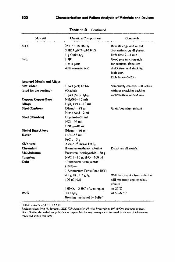
&m Characterization and Failure Analysis of Materials and Devices
Ttbit 11*3 Continued
Maiedal Chemical Coni|>osition Comments
mi
Skti
A^soited Met»ls and Albys S^fls«^der (Used for die bonding)
Alleys Steel (Carbim)
Sled (Stainiesss)
Nkkel Base A l b ^
Nkhrionie Chrc^mlttni Molybdemim tUntsten <M4
WTt
25 HF : 18 HHOi
5HOAc/0.lBriilOHiO
l g C u < N 0 3 ) 2
IHF I to 4 paits 40% chromic acid
I pm (vol) HOAc (Glacial) I part (Vol) H Oa KH4OH—10 ml) HiOi (3%)—10 ml Ethanol—98 ml Nitric Acid -1 ml Glyce!tx)l-—30 ml HCI---30 ml HNOa—lO ml Ethanol—^ ml HCl—15 ml PeCl5-5g 2.25-3.75 molar FeClj Bromine-methanol solution Potassium Fenicyanide—30 g NaOH—10 g, H2O—100 ml I Potassium Peiticyanide (10%)— I Ammonium Persulfate (10%) 4.6 g KI, U g I2, 100 ml H2O
IHNO3—3 HCl (Aqua regia) 3 % H2O2
Bromine-methanol (+ FeBr )
Reveals edge and mixed dislocations on all planes. Etch time 2--4 min. Good p--n junction etch for sections. Excellent dislocation and stacking fault etch. Etch time—5-20 s.
Selectively removes soA: solder without attacking backing metallization or heat sink
Grain boundary etchant
Dissolves all metals.
Will dissolve Au from a die but will not attack unalloyed alu-minum At 25°C At 50-60^C
HOAC = Acetic acid, CH3COOH Recipies taken from M. lacques, IEEE 17th Reliability Physics Proceedings 197 (1979) and other sources. No*e: Neither the author nor publisher is responsible for any consequences incurred in the use of information ct^tained witfiin this table.
11.3 Structural Characterization 603
11.3 STRUCTURAL CHARACTERIZATION
11.3.1 Optical Microscopy
Because seeing is believing, virtually every failure analysis investigation starts with some sort of structural examination procedure. Of the potential tools that can be used for this purpose, none are more popular than low-power stereo and standard, higher-power, optical microscopes. Various levels of the decapsulated package structure are routinely examined by optical methods to qualify the pro-cedure and uncover the sought-after evidence of failure. Optical transmission and metallurgical microscopes are the most widely employed scientific instru-ments for these purposes. The former is limited to thin-film devices and struc-tures on transparent substrates, while the latter are useful in imaging opaque objects like circuits on silicon wafers. Since the principles of the common trans-mission and reflection modes of operation are well known to readers, the dis-cussion will focus on descriptions of less common imaging methods.
Additional optical microscopy techniques applicable to powered devices will be discussed in Section 11.5.
11.3.1.1 Nomarski Contrast By illuminating specimens with plane polar-ized light, a significant enhancement in feature contrast is possible because the image can be made to assume a three-dimensional quality. In the Nomarski dif-ferential interference-contrast method, optical microscopes are outfitted with a Wollaston prism that causes the incident plane polarized light to be separated into two beams. One beam passes through the feature of interest, while the other beam is incident nearby. Upon reflection, the two beams are recombined by a second prism above the objective. As a result, a phase change introduced into the object beam by the specimen is converted into an amplitude of color difference. The Nomarski technique is very sensitive to small surface asperities such as etch pits. Such shallow surface depressions in epitaxial films cannot be discerned in the SEM but are readily visible employing Nomarski contrast. Another applica-tion involves resolution of slight thickness variations in thin oxides grown on differently doped silicon regions. After removing the oxide, the step is easily imaged.
11.3.1.2 Scanning Light Microscopy (SLM) Bridging the gap between conventional optical and scanning electron microscopy are imaging methods employing scanned optical beams. Actually, either the beam is scanned past a fixed specimen, or the specimen is scanned past a fixed beam in these micro-scopes. In SLM, images are built up one point at a time, and the whole field is cov-
604 Characterizatif^ and Fmlure Analysis of Materials and Devices
ered by scanning. Lasers are employed as beam sources, prompting the descriptor laser scanning microscope, or LSM. In the reflected light mode, advantages rela-tive to the scanning electron microscope include no sample preparation, no charg-ing or damage of insulating surfaces, imaging through the depth of transparent layers, and the lack of necessity for a vacuum environment (7).
An important difference between the scanning and ordinary optical micro-scopes is the decoupling of magnification (determined by scanning) ^id resolu-tion (determined by the optics). This allows modifications such as confocality, in which a point detector, consisting of a pinhole in front of a photo-diode or -mul-tiplier, is placed at the precise focal point of the image. The detector then receives light from a point source in the specimen, resulting in images that have both a reduced depth of focus and a slightly improved resolution. Points that are not in focus are not imaged, and as a result, the out-of-focus blur is reduced, dra-matically improving image quality.
11.3.1.3 Fluorescent Tracers In this technique fluorescent tracer dyes are applied to device surfaces in order to demarcate or decorate defective sites for further microscopic observation. After application, the tracer dyes penetrate cracks, corrosion products, and regions of delamination. Under ultraviol^ illu-mination the dyes fluoresce and are made visible with the use of appropriate fil-ters. Crevices and pinholes in glass layers and dielectrics have been exposed this way, while in corrosion studies, pH-sensitive fluorescent dyes have been used (11). Employing fluorescent microthermographic imaging (FMI) systems, defects in powered devices have been identified. This technique capitalizes on the temperature-dependent fluorescence of certain rare-earth-metal chelated compounds such as europium thenoyltrifluoroacetonate (EuTTA). When heated, EuTTA fluoresces bright orange (612 nm) when excited by a UV source.
Fluorescent-dye penetrants have long been used to reveal microcracks on machined and ground metal surfaces.
11.3.2 Electron Microscopy
The scanning electron microscope (SEM) and the transmission electron micro-scope (TEM) are indispensable for high-resolution imaging of small structural features. Shrinkage of device dimensions has fostered the increasing use of elec-tron microscopy relative to optical techniques for chip-level examination. In turn, with the inexorable advances in device reduction we will witness the greater use of the scanning point-probe microscopies. [The scanning tunneling (STM) and atomic force (AFM) microscopes make use of atomically sharp probes brought exceedingly close to surfaces as their terrain is scanned. The
11.3 Structural Characterization 605
AFM already plays a role in defining the metrics of features on IC chips and has been used to probe the topography of planarized surfaces. Destined to play a prominent future role in the characterization of nano-sized features and defects, there are presently an insufficient number of applications to issues of concern in this book. Therefore, these techniques will not be discussed further.]
The TEM, like its optical counterpart, is a true microscope because the entire image in both appears at once; and like the optical microscope, diffraction-limited optics govern the resolution, i.e., the wavelength divided by the numeri-cal aperture. This is not true of the SEM, whose resolution is not diffraction lim-ited, and where the image is built bit by bit through scanning a probe beam.
It.3.2.1 Scanning Electron Microscopy There is little doubt that the most v^satile analytical instrument used in failure-analysis studies is the scanning elec-tron microscope. The reason is that the SEM simultaneously allows for microstruc-tural imaging, chemical analysis, and electrical characterization of materials and devices on both tl^ chip and packaging levels. While it may not possess the highest spatial resolution nor be the most sensitive with regard to identifying atoms, the SEM represents an excellent compromise between these two important analytical capabilities within a single instrument that is relatively easy to use and modest in cost. As an imaging tool it exceeds the resolution of the optical microscope by a fac-tor of almost 100, so that features approaching 1 nm in size can be resolved under optimum conditions. Furthermore, the images possess a three-dimensional beauty conferred by the great depth of focus of the electron beam.
The electron optical column of a typical SEM is shown in Fig. 11-6. Electrons are thermionically emitted from tungsten filaments under a potential difference that ranges from ~1 to 50 kV. If higher intensity or greater resolution are required, LaBg and field-emission cathodes, respectively, are available. After passing through condenser and objective lenses, the beam is demagnified to a ~1 nm spot and then raster scanned over the specimen. Beneath the point of beam impingement a teardrop-shaped region ~1 |xm in depth fills the specimen with the products of electron excitation and deexcitation. These include secondary electrons. Auger electrons, and elastic backscattered electrons with successively higher energies of ~ 50 eV, ~ 1000 eV, and ~ 10 to 30 keV (depending on the primary beam energy), respectively.
Each of these kinds of electrons, as well as atomic fluorescent X-rays and other photons, forms the basis of important imaging and analytical techniques. Virtually all of the SEM images in this book are the result of collecting the low-energy secondary electrons. These emanate from surface layers in intensities that vary with topography. More secondary electrons are emitted at sharp comers, edges, and sloped regions than planar surfaces. The magnification is the ratio of
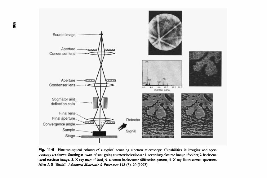
Fig. 11-6 Electron-optical column of a typical scanning electron microscope. Capabilities in imaging and spec-
troscopy are shown. Starting at lower left and going counterclockwise are 1 . secondary electron image of solder, 2. backscat- tered electron image, 3. X-ray map of lead, 4. electron backscatter diffraction pattern, 5. X-ray fluorescence spectrum. After J. B. Bindell, Advanced Materials & Processes 143 (3), 20 (1993).
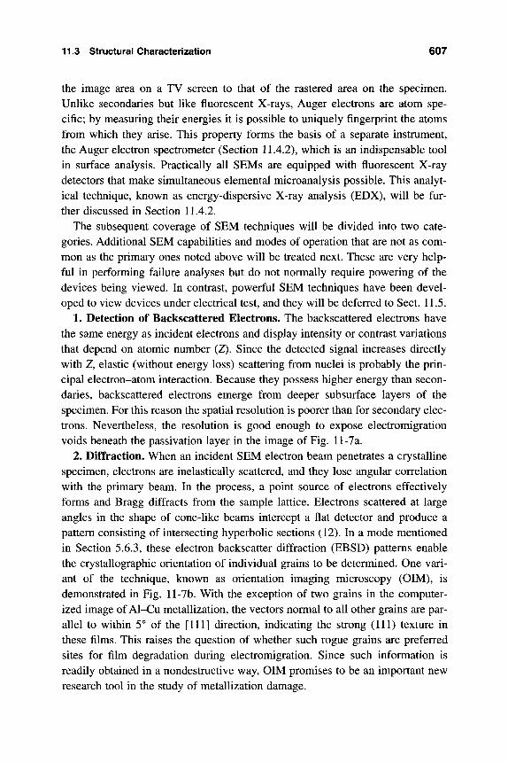
11.3 Structural Characterization 607
the image area on a TV screen to that of the rastered area on the specimen. Unlike secondaries but like fluorescent X-rays, Auger electrons are atom spe-cific; by measuring their energies it is possible to uniquely fingerprint the atoms from which they arise. This property forms the basis of a separate instrument, the Auger electron spectrometer (Section 11.4.2), which is an indispensable tool in surface analysis. Practically all SEMs are equipped with fluorescent X-ray detectors that make simultaneous elemental microanalysis possible. This analyt-ical technique, known as energy-dispersive X-ray analysis (EDX), will be fur-ther discussed in Section 11.4.2.
The subsequent coverage of SEM techniques will be divided into two cate-gories. Additional SEM capabilities and modes of operation that are not as com-mon as the primary ones noted above will be treated next. These are very help-ful in performing failure analyses but do not normally require powering of the devices being viewed. In contrast, powerful SEM techniques have been devel-oped to view devices under electrical test, and they will be deferred to Sect. 11.5.
1. Detection of Backscattered Electrons. The backscattered electrons have the same energy as incident electrons and display intensity or contrast variations that depend on atomic number (Z). Since the detected signal increases directly with Z, elastic (without energy loss) scattering from nuclei is probably the prin-cipal electron-atom interaction. Because they possess higher energy than secon-daries, backscattered electrons emerge from deeper subsurface layers of the specimen. For this reason the spatial resolution is poorer than for secondary elec-trons. Nevertheless, the resolution is good enough to expose electromigration voids beneath the passivation layer in the image of Fig. 11-7a.
2, Diffraction. When an incident SEM electron beam penetrates a crystalline specimen, electrons are inelastically scattered, and they lose angular correlation with the primary beam. In the process, a point source of electrons effectively forms and Bragg diffracts from the sample lattice. Electrons scattered at large angles in the shape of cone-like beams intercept a flat detector and produce a pattern consisting of intersecting hyperbolic sections (12). In a mode mentioned in Section 5.6.3, these electron backscatter diffraction (EBSD) patterns enable the crystallographic orientation of individual grains to be determined. One vari-ant of the technique, known as orientation imaging microscopy (OIM), is demonstrated in Fig. 11-7b. With the exception of two grains in the computer-ized image of Al-Cu metallization, the vectors normal to all other grains are par-allel to within 5° of the [HI] direction, indicating the strong (111) texture in these films. This raises the question of whether such rogue grains are preferred sites for film degradation during electromigration. Since such information is readily obtained in a nondestructive way, OIM promises to be an important new research tool in the study of metallization damage.
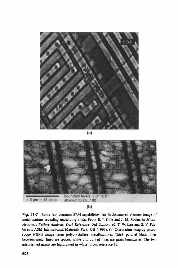
4.5 pm = 45 steps boundary levels: S^"* 15.1 shaded IQ 25...182
(b)
Fig. 11-7 Some less common SEM capabilities, (a) Backscattered electron image of metallizations revealing underlying voids. From E. I. Cole and J. M. Soden, in Micro-electronic Failure Analysis, Desk Reference, 3rd Edition, ed. T. W. Lee and S. V. Pab-bisetty, ASM International, Materials Park, OH (1993). (b) Orientation imaging micro-scope (OIM) image from polycrystalline metallizations. Thick parallel black lines between metal lines are spaces, while thin curved lines are grain boundaries. The two misoriented grains are highlighted in white. From reference 12.
608
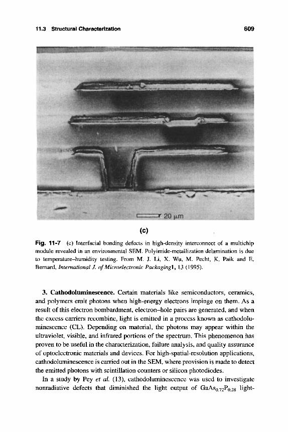
11.3 Structural Characterization 609
a'aOiun
Fig. 11-7 (c) Interfacial bonding defects in high-density interconnect of a multichip module revealed in an environmental SEM. Polyimide-metallization delamination is due to temperature-humidity testing. From M. J. Li, X. Wu, M. Pecht, K. Paik and E. Bernard, IntemationalJ. of Microelectronic Packagingl, 13 (1995).
3. Cathodoluminescence. Certain materials like semiconductors, ceramics, and polymers emit photons when high-energy electrons impinge on them. As a result of this electron bombardment, electron-hole pairs are generated, and when the excess carriers recombine, light is emitted in a process known as cathodolu-minescence (CL). Depending on material, the photons may appear within the ultraviolet, visible, and infrared portions of the spectrum. This phenomenon has proven to be useful in the characterization, failure analysis, and quality assurance of optoelectronic materials and devices. For high-spatial-resolution applications, cathodoluminescence is carried out in the SEM, where provision is made to detect the emitted photons with scintillation counters or silicon photodiodes.
In a study by Fey et al (13), cathodoluminescence was used to investigate nonradiative defects that diminished the light output of GaAso.72Po.28 light-
610 Characterization and Failure Analysis of Materials and Devices
emitting diodes. Black spots roughly 10 |xm in size due to dislocations and stack-ing faults were observed in both p and n regions, and these appeared to be the cause of degradation. In this work GaP-based LEDs were also investigated by CL techniques. Anomalous, multijunction p-n-p-n regions that caused a flicker-ing light output and larger reverse breakdown voltages than good LEDs were observed. In many ways the information gained with CL is similar to that obtained with EBIC (described in Section 11.5.3.2). However, CL does not require the presence of a junction or biasing, but EBIC does. A CL image is reproduced later, in Fig. 11-9c.
4. Thermal Wave Imaging. As in all SEM-based techniques, an electron beam is first scanned across the specimen surface. Energy absorbed at or near the surface results in a periodic heating, which becomes the source of thermal waves that propagate from the heated region (14). The thermal waves interact with, and scatter from, subsurface features that have differing thermal-conduc-tion characteristics from those of the surroundings. In this way thermoacoustic waves are generated at precipitates, doped regions, grain boundaries, dislocation arrays, and cracks. These defects are detected with a piezoelectric transducer and made visible by using the signal they induce to modulate the intensity at a fre-quency of 10 kHz to 10 MHz.
5. Environmental SEM. One of the illusive goals of electron microscopy has been high-resolution structural imaging of specimens not in vacuum, but in the ambient atmosphere. The barriers to achieving this goal are numerous and include corrosion and oxidation of filaments, discharges in the electron optical column, surface charge buildup, and scattering of electrons by the gas mole-cules present in air and humid ambients. To overcome these problems the envi-ronmental SEM, or E-SEM, has been developed. In operation, a gas pressure of -20 torr, rather than ~10~^ torr in a conventional SEM, is maintained in the chamber. The latter is separated from the electron optical column, which oper-ates at high vacuum. Interactions between the probe-beam electrons, signal electrons, and the specimen with the chamber gas are intimately dependent on the pressure, local electric fields, and the operating voltage. Basically, the pos-itively ionized gas molecules bombard regions of negative charge buildup on the specimen surface, neutralizing them. Secondary electrons generated through gas ionization are then collected by a positively biased gaseous detector to form the image.
Li and Pecht (15) have demonstrated the effectiveness of the E-SEM in study-ing thermally induced failures in MMIC devices, water-induced adhesion loss at metal-polyimide interfaces, and temperature-humidity cycling of printed-circuit boards. An E-SEM image is shown in Fig. ll-7c.
11.3 Structural Characterization 611
11.3.3 Transmission Electron IVIicroscopy
Normally a research tool, the transmission electron microscope (TEM) is indis-pensable for the structural imaging of processing and crystallographic defects that are nanometer sized. In comparison, the resolution of the SEM is an order of magnitude poorer. For simplicity, the TEM may be compared to a slide pro-jector with the slide (specimen) illuminated by light (electron beam) that first passes through the condenser lens (electromagnetic condenser lens). The trans-mitted light forms an image that is magnified by the projector lens (electro-magnetic objective and projector lenses) and viewed on a screen (or pho-tographed).
There are several imaging and analytical modes that are noteworthy.
1. Bright field imaging. The directly transmitted beam is used to provide images of the microstructure and morphology of features.
2. Darkfield imaging. Diffracted beam images are used to obtain crystallo-graphic information about structural features.
3. Lattice imaging. A combination of diffracted and direct beams is used to yield images with atomic resolution.
4. Diffraction. Diffraction yields crystallographic and orientation effect infor-mation on defects and phases. Special techniques include microdiffraction and convergent-beam diffraction.
5. X-ray spectroscopy. This analytical capability is basically the same as energy dispersive X-ray (EDX) analysis and allows elemental identification.
6. Electron energy loss spectroscopy (EELS). Through energy analysis of the transmitted electron-beam, composition analysis is possible. EELS is useful for detecting low-Z elements.
Further details of the electron optics and operational modes of these and other TEM modes of operation have been discussed in many books; the recent one by Williams and Carter (16) is a recommended source of this information.
A primary disadvantage of TEM methods is that specimens must be very thin, e.g., 100-1000 nm thick, to enable electrons to penetrate them. For failure analy-sis purposes this frequently presents a significant time-consuming experimental challenge, which additionally destroys devices and components in the process of sample preparation. This, combined with its poor selectivity of location, rele-gates the TEM to identifying specific microscopic failure mechanisms, particu-larly those involving the roles of dislocations, precipitates, and crystalline per-fection. In this way TEM methods have played a crucial role in exposing subtle defects that limit yield and lead to reliability problems. Due to the limitations
612 Characterization and Faiiure Analysis of Materials and Devices
noted above, the SEM is now the preferred tool for structural evaluation in fail-ure analysis.
If, however, one has the luxury of time, which is normally absent in the FMA laboratory environment, it is now possible to prepare thin specimens having almost any orientation with respect to an IC chip or device. Examples were shown previously in the laser defects depicted in Figs. 10-8 and 10-10. The extra effort made in obtaining these images gives truth to the adage that "one picture is worth a thousand words."
Perhaps the most dramatic images of devices are those taken in cross-section. In this important technique, specimens that are already thin in one dimension are now thinned in the transverse direction; it is like imaging this page in edge view rather than in the plane the words appear on. What is involved in the case of ICs is cleaving a number of wafer specimens transversely, bonding these slivers in an epoxy button, and thinning them by grinding and polishing. Finally, the resulting disc is ion milled until a hole appears. By preparing many specimens simultaneously, the probability of capturing images from the desired circuit fea-tures is enhanced. In this way the striking images shown Figs. 3-8a and 10-8c were obtained.
11.3.4 Focused Ion Beams
The use of focused ion beams (FIB) provides two additional capabilities to the failure analyst. First, the FIB can be operated as a high-resolution microscope that has some advantages (and disadvantages) relative to the SEM and TEM. Briefly, the FIM resembles an SEM, but instead of electrons, gallium ions gen-erated in a liquid-metal ion source are employed as the imaging vehicle. In the optical column these ions are electrostatically focused into a fine beam that raster scans the specimen surface, releasing secondary electrons for structural imaging. The FIB image of the interconnect shown in Fig. 5-18b reveals grain orientation contrast unlike SEM imaging; also unlike the TEM, no sample prepa-ration is required in FIB microscopy.
At the same time as the Ga ions help form images, they contaminate speci-mens, introduce artifacts, and sputter away the material being observed. The last of these undesirable features for imaging is turned to good advantage in prepar-ing TEM cross-sections, where it has eased the drudgery and eliminated the ele-ment of chance in locating features for examination (17). Operating like a milling machine, the 10 to 25 keV Ga beam precisely ablates material from sub-micron regions of specimens. Suitably thinned features can then be readily examined in the TEM. This sample preparation technique, illustrated in Fig. 11-8 has greatly advanced failure-analysis methodology.
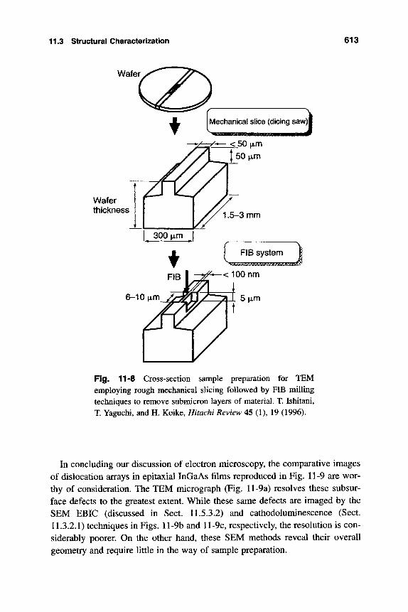
11.3 Structural Characterization 613
Wafer
Wafer thicl<ness
6-10 jim
Fig. 11-8 Cross-section sample preparation for TEM employing rough mechanical slicing followed by FIB milling techniques to remove submicron layers of material. T. Ishitani, T. Yaguchi, and H. Koike, Hitachi Review 45 (1), 19 (1996).
In concluding our discussion of electron microscopy, the comparative images of dislocation arrays in epitaxial InGaAs films reproduced in Fig. 11-9 are wor-thy of consideration. The TEM micrograph (Fig. 11-9a) resolves these subsur-face defects to the greatest extent. While these same defects are imaged by the SEM EBIC (discussed in Sect. 11.5.3.2) and cathodoluminescence (Sect. 11.3.2.1) techniques in Figs. 11-9b and 11-9c, respectively, the resolution is con-siderably poorer. On the other hand, these SEM methods reveal their overall geometry and require little in the way of sample preparation.
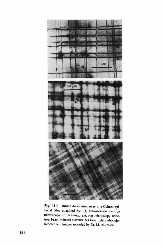
Fig. 11-9 Buried dislocation array in a GalnAs epi-taxial film imagined by: (a) transmission electron microscopy, (b) scanning electron microscopy (elec-tron beam induced current), (c) total light cathodolu-minescence. Images recorded by Dr. M. Al-Jassim.
614
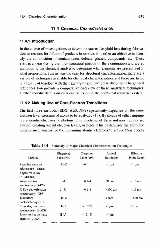
11.4 Chemical Characterization 615
11.4 CHEIVIICAL CHARACTERIZATION
11.4.1 Introduction
In the course of investigations to determine causes for yield loss during fabrica-tion or reasons for failure of products in service, it is often an objective to iden-tify the composition of contaminants, defects, phases, compounds, etc. These entities appear during the microstructural portion of the examination and are an invitation to the chemical analyst to determine what elements are present and in what proportions. Just as was the case for structural characterization, there are a variety of techniques available for chemical characterization, and these are listed in Table 11-4 together with their acronyms and particular attributes. The general references 1 ^ provide a comparative overview of these analytical techniques. Further specific details on each can be found in the additional references cited.
11.4.2 Making Use of Core-Electron Transitions
The first three methods (EDX, AES, XPS) specifically capitalize on the core-electron level structure of atoms to be analyzed (18). By means of either imping-ing energetic electrons or photons, core electrons of these unknown atoms are ejected, creating vacant electron levels, or holes. This destabilizes the atom and initiates mechanisms for the remaining atomic electrons to reduce their energy
Table 11-4 Summary of Major Chemical Characterization Techniques
Method
Scanning electron microscope—energy dispersive X-ray (SEM/EDX) Auger electron spectroscopy (AES) X-Ray photoelectron spectroscopy (XPS) Rutherford backscattering (RBS) Secondary ion mass spectrometry (SIMS) Laser ionization mass analysis (LIMA)
Elemental Sensitivity
Na-U
Li-U
Li-U
He-U
H-U
H-U
Detection Limit (at%)
~0. I
-0.1-1
-0.1-1
-1
-10"^%
-10"Vo
Lateral Resolution
-1 |xm
50 nm
-100 |im
1 mm
- I ^im
- I |xm
Effective Probe Depth
- 1 jim
-1.5 nm
-1.5 nm
-20.0 nm
1.5 nm
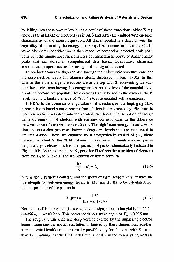
616 Characterization and Failure Analysis of Materials and Devices
by falling into these vacant levels. As a result of these transitions, either X-ray photons (as in EDX) or electrons (as in AES and XPS) are emitted with energies characteristic of the atom in question. All that is needed is a detector with the capability of measuring the energy of the expelled photons or electrons. Quali-tative elemental identification is then made by comparing detected peak posi-tions with the unique spectral signatures of characteristic X-ray or Auger energy peaks that are stored in computerized data bases. Quantitative elemental amounts are proportional to the strength of the signal detected.
To see how atoms are fingerprinted through their electronic structure, consider the core-electron levels for titanium atoms displayed in Fig. 11-10a. In this scheme the most energetic electrons are at the top with 0 representing the vac-uum level; electrons having this energy are essentially free of the material. Lev-els at the bottom are populated by electrons tightly bound to the nucleus; the K level, having a binding energy of 4966.4 eV, is associated with s electrons.
1. EDX. In the conmion configuration of this technique, the impinging SEM electron beam knocks out electrons from all levels simultaneously. Electrons in more energetic levels drop into the vacated state levels. Conservation of energy demands emission of photons with energies corresponding to the difference between those of the two involved levels. The high beam energy means absorp-tion and excitation processes between deep core levels that are manifested in emitted X-rays. These are captured by a cryogenically cooled Si (Li) diode detector attached to the SEM colunm and converted through standard pulse-height analysis electronics into the spectrum of peaks schematically indicated in Fig. 11-lOb. As an example, the K^ peak for Ti reflects the transition of electrons from the L3 to K levels. The well-known quantum formula
Y = ^ 2 - ^ i (11-6)
with h and c Planck's constant and the speed of light, respectively, enables the wavelength (k) between energy levels E2 (L3) and E^K) to be calculated. For this purpose a useful equation is
1 24 X (^m) = -'^ . (11-7)
[£2-^ i ] (eV) Noting that all binding energies are negative in sign, substitution yields [- 455.5 -(-4966.4)] = 4510.9 eV. This corresponds to a wavelength of K« = 0.275 nm.
The roughly 1 |im wide and deep volume excited by the impinging electron beam means that the spatial resolution is limited by these dimensions. Further-more, atomic identification is normally possible only for elements with Z greater than 11, implying that the EDX technique is ideally suited to analyzing metallic
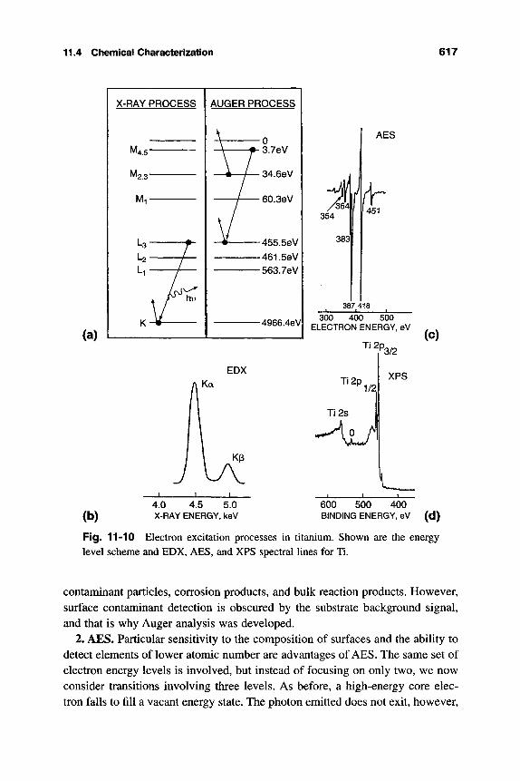
11.4 Chemical Characterization 617
(a)
X-RAY PROCESS
(b)
M.
M. "2.3"
Mi
AUGER PROCESS
0 3.7eV
34.6eV
60.3eV
455.5eV 461.5eV 563.7eV
-4966.4eV
354
AES
387 418
300 400 500 ELECTRON ENERGY, eV
Ti2p, (C)
EDX TI2p
3/2
XPS
4.0 4.5 5.0 X-RAY ENERGY, keV
600 500 400 BINDING ENERGY, eV (d)
Fig, 11-10 Electron excitation processes in titanium. Shown are the energy level scheme and EDX, AES, and XPS spectral lines for Ti.
contaminant particles, corrosion products, and bulk reaction products. However, surface contaminant detection is obscured by the substrate background signal, and that is why Auger analysis was developed.
2. AES. Particular sensitivity to the composition of surfaces and the ability to detect elements of lower atomic number are advantages of AES. The same set of electron energy levels is involved, but instead of focusing on only two, we now consider transitions involving three levels. As before, a high-energy core elec-tron falls to fill a vacant energy state. The photon emitted does not exit, however,
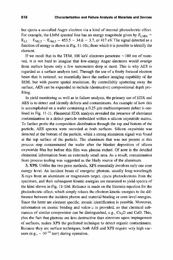
618 Characterization and Failure Analysis of Materials and Devices
but ejects a so-called Auger electron via a kind of internal photoelectric effect. For example, the LMM spectral line has an energy magnitude given by ^LMM ^ EL3 ~ EM2,3 ~ EM4,5 = 455.5 - 34.6 - 3.7, or 417 eV The signal detected as a function of energy is shown in Fig. 11-lOc, from which it is possible to identify the element.
If we recall that in the TEM, 100 keV electrons penetrate —100 nm of mate-rial, it is not hard to imagine that low-energy Auger electrons would emerge from surface layers only a few nanometers deep at most. This is why AES is regarded as a surface analysis tool. Through the use of a finely focused electron beam that is rastered, we essentially have the surface imaging capability of the SEM, but with poorer spatial resolution. By controllably sputtering away the surface, AES can be expanded to include (destructive) compositional depth pro-filing.
In yield monitoring as well as in failure analysis, the primary use of EDX and AES is to detect and identify defects and contaminants. An example of how this is accomplished on a wafer containing a 0.25 |xm multicomponent defect is out-lined in Fig. 11-11. Elemental EDX analysis revealed the presence of aluminum contamination in a defect particle embedded within a silicon oxynitride matrix. To further probe the composition distribution through the top and bottom of the particle, AES spectra were recorded at both surfaces. Silicon oxynitride was detected at the bottom of the particle, while a strong aluminum signal was found at the top surface of the particle. The aluminum that was not present at this process step contaminated the wafer after the blanket deposition of silicon oxynitride film but before this film was plasma etched. Of note is the detailed elemental information from an extremely small area. As a result, contamination from process tooling was suggested as the likely source of the aluminum.
3. XPS. Unlike the two prior methods, XPS essentially involves only one core energy level. An incident beam of energetic photons, usually long-wavelength X-rays from an aluminum or magnesium target, ejects photoelectrons from the specimen, and their subsequent kinetic energies are measured to yield spectra of the kind shown in Fig. 11-lOd. Reliance is made on the Einstein equation for the photoelectric effect, which simply relates the electron kinetic energies to the dif-ference between the incident photon and material binding or core-level energies. Since the latter are element specific, atomic identification is possible. Moreover, information on atomic binding and valence is provided, so that chemical sub-stances of similar composition can be distinguished, e.g., CU2O and CuO. This, plus the fact that photons are less destructive than electrons upon impingement of surfaces, makes XPS the preferred technique to detect organic contaminants. Because they are surface techniques, both AES and XPS require very high vac-uum (e.g., ~ 10"^^ torr) during operation.
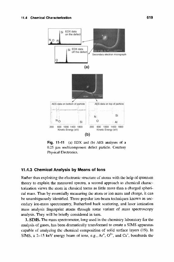
11.4 Chemical Characterization 619
jSi EDXdata 1 on the defect
N^AJ
1 Si EDX data 1 off the defect
sJ (a)
AES data on bottom of particle
J
Si
AES data on top of particle
Si
A!
200 600 1000 1400 1800 Kinetic Energy (eV)
200 600 1000 1400 1800 Kinetic Energy (eV)
(b)
Fig. 11-11 (a) EDX and (b) AES analyses of a 0.25 |im multicomponent defect particle. Courtesy Physical Electronics.
11.4.3 Chemical Analysis by Means of Ions
Rather than exploiting the electronic structure of atoms with the help of quantum theory to explain the measured spectra, a second approach to chemical charac-terization views the atom in classical terms as little more than a charged spheri-cal mass. Thus by essentially measuring the atom or ion mass and charge, it can be unambiguously identified. Three popular ion-beam techniques known as sec-ondary ion-mass spectrometry, Rutherford back scattering, and laser ionization mass analysis fingerprint atoms through some variant of mass spectroscopy analysis. They will be briefly considered in turn.
1. SIMS. The mass spectrometer, long used in the chemistry laboratory for the analysis of gases, has been dramatically transformed to create a SIMS apparatus capable of analyzing the chemical composition of solid surface layers (19). In SIMS, a 2-15 keV energy beam of ions, e.g., Ar^, O^", and Cs" , bombards the
620 Characterization and Fatiure Analysis of l\/laterials and Devices
surface and spotters neutral atoms, for the most part, but also positive and nega-tive ions from the outermost surface layers. Once in the gas phase, the ions and molecular fragments are mass analyzed in order to identify the species present as well as determine their abundance. The charged sputtered particles are first extracted, and they then enter an energy analyzer consisting of a magnetic-sector mass filter whose function is to select a particular mass for detection. The desired ion of mass m, charge q, and velocity v traces a specific arc of radius r in the magnetic field {B) of an electromagnet, given by r = mv/{qB). In this way the ions are separated, and a spectrum of peaks representing individual masses is obtained. The advantage of high-detection sensitivity is offset by an extremely complex spectrum of peaks corresponding to the masses of ions and ion frag-ments. Standards, composed of the specific elements and matrices in question, are thus necessary for quantitative determinations of composition.
Depth profiling of ion-implanted dopants in various portions of devices is the primary application of SIMS in semiconductor technology. Better than part-per-million atom-fraction detection sensitivities are achieved. In the area of failure analysis SIMS has been used (20) to detect
a. carbon and oxygen at critical interfaces of multilayer metallizations; b. mobile ion contamination of good and leaky transistors and diodes; c. transport of mobile ions through passivation layers; d. relative levels of hydrogen, chlorine, and fluorine in thick oxides and nitrides.
2. RBS. This technique relies on the use of very high energy (e.g., 2 MeV) beams of low mass ions that are incident on a film-substrate combination (21). The ions, typically "He"*", lose energy through
1. transiting the specimen during penetration, 2. binary elastic collisions with matrix atoms that result in ion backscatter 3. retraversing the material to exit it.
The magnitudes of all of these energy losses are well known; the first and third are due to both electronic excitation and nuclear collisions. However, the largest contribution to energy loss of the probe ion stems from the momentum transfer in the elastic collision between ion and atom. By measuring the number and energy distribution of the backscattered ions, it is possible to work back-wards and obtain information on the nature of the elements present and their concentration and depth distribution, all without appreciably damaging the spec-imen. In this way, compound compositions, thicknesses, and distributions can be accurately ascertained without the use of standards. Within its realm of applica-bility, RBS is the preferred choice relative to EDX, AES, XPS, and SIMS because it is intrinsically quantitative and requires no calibration.
11.5 Examining Devices Under Electrical Stress 621
Poor spatial resolution limits RBS to scientific investigation of broad-area (blanket) multicomponent thin-film layers rather than to similar film structures in actual devices. Thus it is the perfect tool to quantitatively study the reactions between aluminum and gold films, for example, but purple plague formation at an actual contact is more profitably studied with SEM/EDX.
3. LIMA. Rather than remove surface atoms for analysis through ion impact as in SIMS, they are blasted off the surface by miniexplosions using a finely focused laser beam. The ions so created move through a time-of-flight drift tube, where their mass-to-charge ratio is determined by measuring their velocity in a fixed electric field. This information enables identification of the atoms.
11.5 EXAMINING DEVICES UNDER ELECTRICAL STRESS
11.5.1 Introduction
All of the analytical and diagnostic methods presented so far have one major shortcoming—the materials and devices are not viewed under use conditions. In certain cases such as failure, post-mortem examination of the remains may be the only practical course. Even during quality or yield testing, structural and chemical analyses are always easier to perform when devices are not electrically powered, heated, or otherwise exposed to operating variables. But this momen-tary advantage of ease in measurement may be offset by difficulty in interpret-ing and applying the results of analysis. This section is devoted to exploring those techniques that have been developed to provide information on local charge transport and heating effects in powered devices. As we shall see, the structural resolution possible in these in situ methcKis generally falls short of electron microscope capabilities; but greater sensitivity to local damage and abil-ity to monitor time-dependent change are important advantages.
11.5.2 Emission Microscopy
This exciting new advance in probing and imaging damage sites in integrated cir-cuits is built around an optical microscope (22,23). A schematic of the light emis-sion microscopy (LEM) technique is shown in Fig. 11-12, This method employs light of variable wavelength, typically in the range 400-1000 nm, which impinges on an IC chip electrically powered by a circuit tester. In response to optical stim-ulation, weak luminescence occurs locally at defects. The emitted photon signal is captured and amplified with a sensitive photomultiplier-detector, enabling the
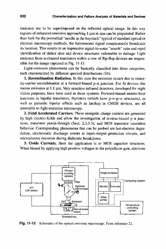
622 Characterization and Faiiure Analysis of l\/lateriais and Devices
emission site to be superimposed on the reflected optical image. In this way regions of enhanced emission approaching 1 |Lim in size can be pinpointed. Rather than look for the proverbial ''needle in the haystack" typical of standard optical or electron microscopy methods, the luminescent signal conspicuously broadcasts its location. This results in an impressive signal-to-noise "search" ratio and rapid identification of defect sites and device structures vulnerable to damage. Light emission from n-channel transistors within a row of flip-flop devices are respon-sible for the image captured in Fig. 11-13.
Light-emission phenomena can be basically classified into three categories, each characterized by different spectral distributions (24).
1. Recombination Radiation. In this case the emission occurs due to minor-ity-carrier recombination at a forward-biased p-n junction. For Si devices this means emission at 1.1 |Lim. Very sensitive infrared detectors, developed for night vision purposes, have been used in these systems. Forward-biased emitter-base junctions in bipolar transistors, thyristors (which have p-n-p-n structures), as well as parasitic bipolar effects such as latchup in CMOS devices, are all amenable to light-emission microscopy.
2. Field Accelerated Carriers. These energetic charge carriers are generated by high electric-fields and allow the investigation of reverse-biased p-n junc-tions, transistor punch-through (Sect. 2.3.3.3), and MOS transistor saturation behavior. Corresponding phenomena that can be probed are hot-electron degra-dation, electrostatic discharge events at input-output protection circuits, and microplasma emission during dielectric breakdown.
3. Oxide Currents. Here the application is to MOS capacitor structures. When biased by applying high positive voltages to the polysilicon gate, electrons
Computing system
Shielded box
Fig. 11-12 Schematic of the optical emission microscope. From reference 22.
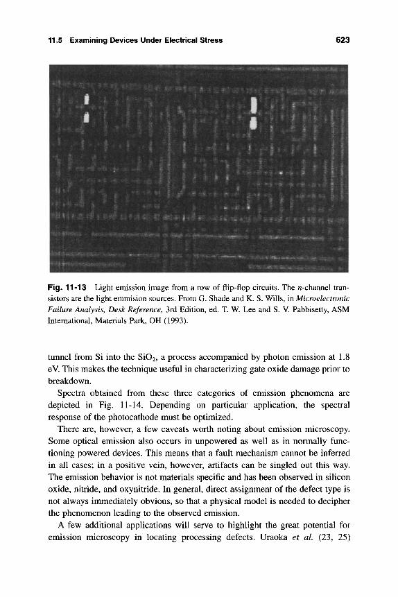
11.5 Examining Devices Under Electrical Stress 623
Fig. 11-13 Light emission image from a row of flip-flop circuits. The n-channel tran-sistors are the light emmision sources. From G. Shade and K. S. Wills, in Microelectronic Failure Analysis, Desk Reference, 3rd Edition, ed. T. W. Lee and S. V. Pabbisetty, ASM International, Materials Park, OH (1993).
tunnel from Si into the Si02, a process accompanied by photon emission at L8 eV. This makes the technique useful in characterizing gate oxide damage prior to breakdown.
Spectra obtained from these three categories of emission phenomena are depicted in Fig. 11-14. Depending on particular application, the spectral response of the photocathode must be optimized.
There are, however, a few caveats worth noting about emission microscopy. Some optical emission also occurs in unpowered as well as in normally func-tioning powered devices. This means that a fault mechanism cannot be inferred in all cases; in a positive vein, however, artifacts can be singled out this way. The emission behavior is not materials specific and has been observed in silicon oxide, nitride, and oxynitride. In general, direct assignment of the defect type is not always inmiediately obvious, so that a physical model is needed to decipher the phenomenon leading to the observed emission.
A few additional applications will serve to highlight the great potential for emission microscopy in locating processing defects. Uraoka et al. (23, 25)
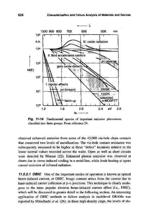
624 Characterization and Failure Analysis of Materials and Devices
1000 900 800 700 : i — I r
600 500 nm
N(E)
2.4 eV 2.6
Fig. 11-14 Fundamental spectra of important emission phenomena classified into three groups. From reference 24.
observed enhanced emission from some of the 45,000 via-hole chain contacts that connected two levels of metallization. The via-hole contact resistance was subsequently measured to be higher at these "defect" locations relative to the lower normal values recorded across the wafer. Open as well as short circuits were detected by Murase (22). Enhanced photon emission was observed at shorts due to stress-induced voiding in a metal line, while Joule heating at opens caused emission of infrared radiation.
11.5.2.1 OBIC One of the important modes of operation is known as optical beam-induced current, or OBIC. Image contrast arises from the current due to laser-induced carrier collection at p-n junctions. This technique is clearly analo-gous to the more popular electron beam-induced current effect (i.e., EBIC), which will be discussed in greater detail in the following section. An interesting application of OBIC methods to failure analysis in multilevel DRAMs was reported by Mitsuhashi et al (26). In these high-density chips, the levels of alu-
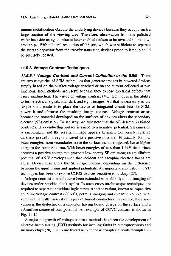
11.5 Examining Devices Under Electrical Stress 625
minum metallization obscure the underlying devices because they occupy such a large fraction of the viewing area. Therefore, observation from the polished wafer backside using an infrared laser enabled defects to be revealed in the pow-ered chips. With a lateral resolution of 0.8 |Lim, which was sufficient to separate the storage capacitor from the transfer transistor, devices prone to latchup could be precisely located.
11.5.3 Voitoge Contrast Techniqims
11.5,3.1 Voltage Contrast and Current Collection in the SEM There are two categories of SEM techniques tiiat generate images in powered devices simply based on the surface voltage reached or on the current collected at p-4i junctions. Both methods are useful because they expose electrical defects that cause malfunction. The virtue of voltage contrast (VC) techniques is the ability to turn electrical signals into dark and light images. All that is necessary in the simple static mode is to place the device or integrated circuit into the SEM, power it and observe the resulting image contrast. Voltage contrast arises because the potential developed on the surfaces of devices alters the secondary electron (SE) emission. To see why, we first note that the SE detector is biased positively. If a conducting surface is raised to a negative potential, SE emission is encouraged, and the resultant image appears brighter. Conversely, relative darkness prevails in regions raised to a positive potential. Physically, for low beam energies more secondaries leave the surface than are injected, but at higher energies the reverse is true. With beam energies of less than 1 keV the surface acquires a positive charge that prevents low-energy SE emission; an equilibrium potential of 0.5 V develops such that incident and escaping electron fluxes are equal. Device bias alters the SE image contrast depending on the difference between the equilibrium and applied potentials. An important application of VC techniques has been to expose CMOS devices sensitive to latchup (27).
Voltage contrast methods have been extended to enable dynamic imaging of devices under specific clock cycles. In such cases stroboscopic techniques are required to separate individual logic states. Another variant, known as capacitive coupling voltage contrast (CCVC), permits imaging and dynamic voltage mea-surement beneath passivation layers of buried conductors. In essence, the passi-vation is the dielectric of a capacitor having bound charge on the surface and a subsurface source of bias potential. An example of CCVC contrast is shown in Fig. 11-15.
A major outgrowth of voltage contrast methods has been the development of electron beam testing (EBT) methods for locating faults in microprocessors and memory chips (28). Faults are traced back in these complex circuits through sue-
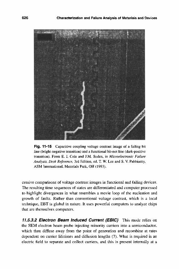
626 Characterization and Failure Analysis of l\/laterials and Devices
Fig. 11-15 Capacitive coupling voltage contrast image of a failing bit line (bright-negative transition) and a functional bit-not line (dark-positive transition). From E. I. Cole and J.M. Soden, in Microelectronic Failure Analysis, Desk Reference, 3rd Edition, ed. T. W. Lee and S. V. Pabbisetty, ASM International, Materials Park, OH (1993).
cessive comparisons of voltage contrast images in functional and failing devices. The resulting time sequences of states are differentiated and computer processed to highlight divergences in what resembles a movie loop of the nucleation and growth of faults. Rather than conventional voltage contrast, which is a local technique, EBT is global in nature. It uses powerful computers to analyze chips that are themselves computers.
77.5.3.2 Electron Beam Induced Current (EBIC) This mode relies on the SEM electron beam probe injecting minority carriers into a semiconductor, which then diffuse away from the point of generation and recombine at rates dependent on carrier lifetimes and diffusion lengths (7). What is required is an electric field to separate and collect carriers, and this is present internally at a
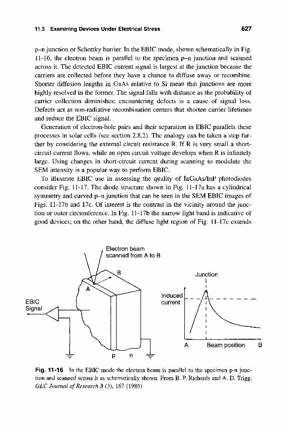
11.5 Examining Devices Under Electrical Stress 627
p-n junction or Schottky barrier. In the EBIC mode, shown schematically in Fig. 11-16, the electron beam is parallel to the specimen p-n junction and scanned across it. The detected EBIC current signal is largest at the junction because the carriers are collected before they have a chance to diffuse away or recombine. Shorter diffusion lengths in GaAs relative to Si mean that junctions are more highly resolved in the former. The signal falls with distance as the probability of carrier collection diminishes; encountering defects is a cause of signal loss. Defects act as non-radiative recombination centers that shorten carrier lifetimes and reduce the EBIC signal.
Generation of electron-hole pairs and their separation in EBIC parallels these processes in solar cells (see section 2.8.2). The analogy can be taken a step fur-ther by considering the external circuit resistance R. If R is very small a short-circuit current flows, while an open circuit voltage develops when R is infinitely large. Using changes in short-circuit current during scanning to modulate the SEM intensity is a popular way to perform EBIC.
To illustrate EBIC use in assessing the quality of InGaAs/InP photodiodes consider Fig. 11-17. The diode structure shown in Fig. ll-17a has a cylindrical symmetry and curved p-n junction that can be seen in the SEM EBIC images of Figs. ll-17b and 17c. Of interest is the contrast in the vicinity around the junc-tion or outer circumference. In Fig. 11-17b the narrow light band is indicative of good devices; on the other hand, the diffuse light region of Fig. ll-17c extends
Electron beam scanned from A to B
Junction
EBIC Induced current
Beam position B
Fig. 11-16 In the EBIC mode the electron beam is parallel to the specimen p-n junc-tion and scanned across it as schematically shown. From B. P. Richards and A. D. Trigg, GEC Journal of Research 3 (3), 167 (1985)
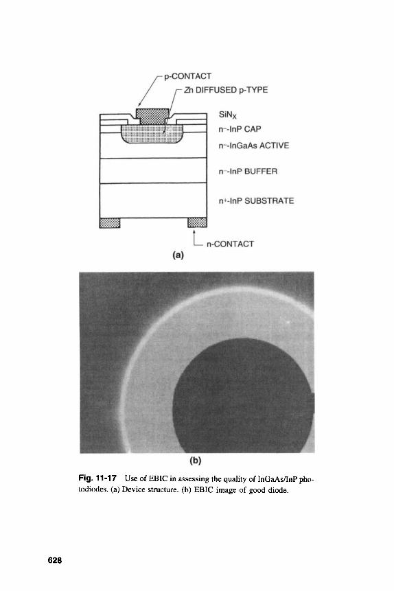
p-CONTACT
2h DIFFUSED p-TYPE
lii'iliiii"';;i';i'';"ffi;J;h!h;I
SiNx
n-lnP CAP
n-lnGaAs ACTIVE
n--lnP BUFFER
n+-lnP SUBSTRATE
r„. CONTACT (a)
Fig. 11-17 Use of EBIC in assessing the quality of InGaAs/InP pho-todiodes. (a) Device structure, (b) EBIC image of good diode.
628
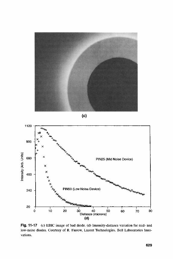
1120
900 H
680
X X
^ X
+
C
<
^ 460 H
240
20
\ \
++»-, PIN25 (Mid Noise Device)
X
X
++.
X X X
^=H+.. ^+H,
"^•Hti.,
\ PIN50 (Low Noise Device) * ^ H *»=H:tftH.
< ^ —I 1 1 I T~ 10 20 30 40 50
Distance (microns)
(d)
60 70 80
Fig. 11-17 (c) EBIC image of bad diode, (d) Intensity-distance variation for mid- and low-noise diodes. Courtesy of R. Farrow, Lucent Technologies, Bell Laboratories Inno-vations.
629
630 Characterization and Failure Analysis of l\/lateriais and Devices
deeply into the n-type InGaAs and is indicative of poor device behavior. The spatially distributed intensity (not collected current) is quantitatively displayed in Fig. ll-17d where brighter regions are associated with defects, charge recom-bination centers, and inhomogeneous doping.
11.5.3.3 Voltage Contrast by Focused Ion Beams This probeless voltage-contrast technique, the subject of a recent publication (29), uses a focused ion beam to isolate defects in ultralage-scale integrated circuits, e.g., 64 Mb and 256 Mb DRAMs with line widths as small as 0.25|J.m. In device mazes of such small dimensions, common defect exposure methods such as light emis-sion microscopy, OBIC, and liquid-crystal probing are severely challenged. The positive focused ion beam in the voltage-contrast technique charges floating structures on the chip, establishing a potential difference between them and ground. As a result, the secondary electron image tends to be attenuated at such structures, making them visible in the electron imaging mode. In this sense the technique parallels that of SEM voltage-contrast (Sect. 11.5.3.1). However, the FIB technique can be leveraged to ion mill defective regions in order to delayer them and expose cross-sections for further in situ examination; therein lies its great advantage. In practice, light emission microscopy or OBIC first locates the approximate defect position, after which it is precisely marked at high resolution by FIB. Failure modes for which the technique is applicable include deep trench capacitor polysilicon to substrate leakage, gate conductor to self-aligned contact shorts, metal line opens, via chain opens, and metal line to line shorts.
11.5.4 Thermography
Joule heating is often a consequence of circuit function. However, when circuits contain components or devices that are in the process of degrading or have failed, the local temperature rises above the "normal" Joule heating level. Ther-mography broadly encompasses a class of experimental techniques having the capability of imaging the heat distribution in objects. In particular, several meth-ods that have been developed to pinpoint the location of heat generation in inte-grated circuits and electrical equipment are considered next.
11.5.4.1 Liquid Crystal Imaging In this technique liquid crystals (LC) are the temperature sensing element (30). For this purpose nematic liquid crystals, in which rod-shaped molecules align along a unique axis, are used. Below a criti-cal first-order phase-transition temperature known as the clearing point (re), the crystals are aligned, and the liquid is optically anisotropic. This means that if the LC is imaged between a pair of crossed polarizers (analyzer and polarizer at
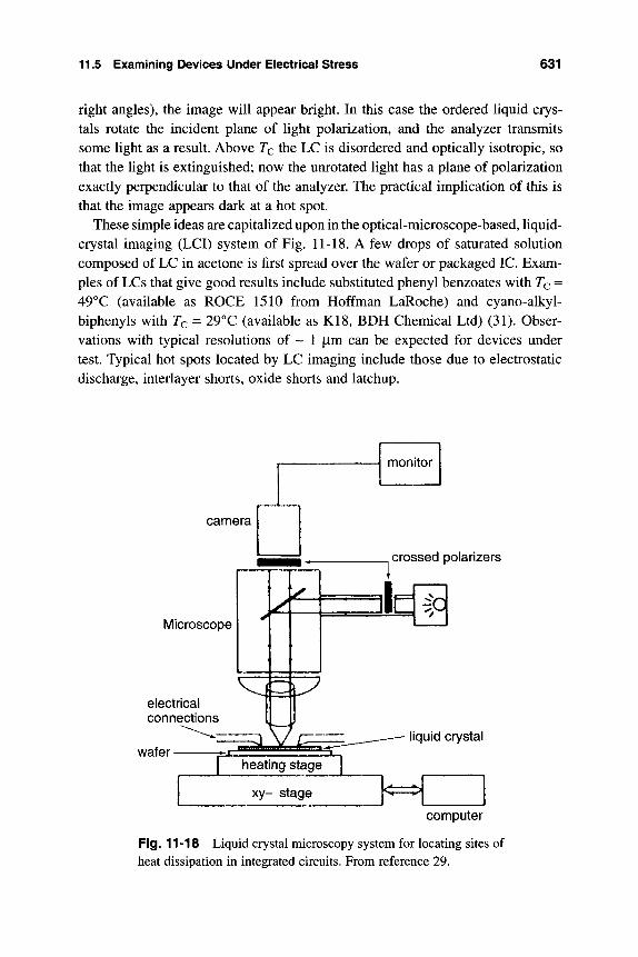
11.5 Examining Devices Under Electrical Stress 631
right angles), the image will appear bright. In this case the ordered Hquid crys-tals rotate the incident plane of light polarization, and the analyzer transmits some light as a result. Above TQ the LC is disordered and optically isotropic, so that the light is extinguished; now the unrotated light has a plane of polarization exactly perpendicular to that of the analyzer. The practical implication of this is that the image appears dark at a hot spot.
These simple ideas are capitalized upon in the optical-microscope-based, liquid-crystal imaging (LCI) system of Fig. 11-18. A few drops of saturated solution composed of LC in acetone is first spread over the wafer or packaged IC. Exam-ples of LCs that give good results include substituted phenyl benzoates with TQ = 49°C (available as ROCE 1510 from Hoffman LaRoche) and cyano-alkyl-biphenyls with Tc = 29°C (available as K18, BDH Chemical Ltd) (31). Obser-vations with typical resolutions of ~ 1 |Lim can be expected for devices under test. Typical hot spots located by LC imaging include those due to electrostatic discharge, interlayer shorts, oxide shorts and latchup.
camera
Microscope
electrical connections
wafer
J ^
monitor
crossed polarizers
Jd^
liquid crystal
1 heating stage |
xy- stage
computer
Fig. 11-18 Liquid crystal microscopy system for locating sites of heat dissipation in integrated circuits. From reference 29.
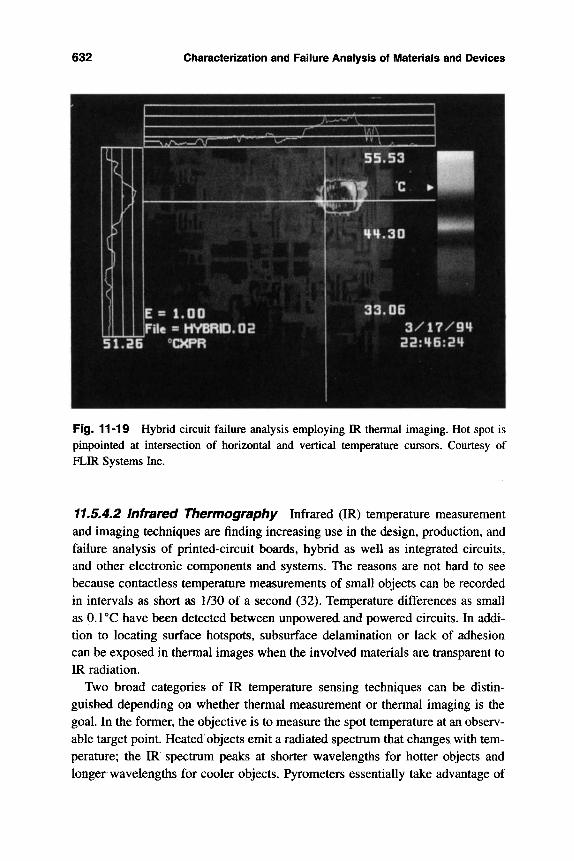
632 Characterization and Failure Analysis of l\/laterials and Devices
5 5 . 5 3
H f . 3 0
1 :' M £ = l .DO i!e =• HYBRID. Or2
5 1 , SB CXPR
33.06 3 / 1 7 / 9 1
Fig. 11-19 Hybrid circuit failure analysis employing IR thermal imaging. Hot spot is pinpointed at intersection of horizontal and vertical temperature cursors. Cotirtesy of FLIR Systems Inc.
11.5.4.2 Infrared Thermography Infrared (IR) temperature measurement and imaging techniques are finding increasing use in the design, production, and failure analysis of printed-circuit boards, hybrid as well as integrated circuits, and other electronic components and systems. The reasons are not hard to see because contactless temperature measurements of small objects can be recorded in intervals as short as 1/30 of a second (32). Temperature differences as small as 0.1 °C have been detected between unpowered and powered circuits. In addi-tion to locating surface hotspots, subsurface delamination or lack of adhesion can be exposed in thermal images when the involved materials are transparent to IR radiation.
Two broad categories of IR temperature sensing techniques can be distin-guishad depending on whether thermal measurement or thermal imaging is the goal. In the former, the objective is to measure the spot temperature at an observ-able target point. Heated objects emit a radiated spectrum that changes with tem-perature; the IR spectrum peaks at shorter wavelengths for hotter objects and longer wavelengths for cooler objects. Pyrometers essentially take advantage of
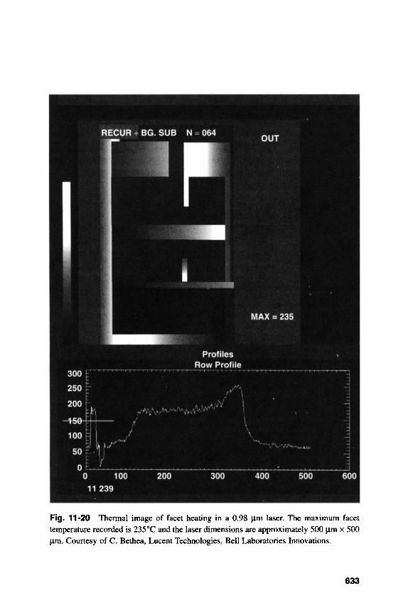
RECUR + BG. SUB N = 064
MAX = 235
Profiles Row Profile
0 100
11 239
Fig. 11-20 Thermal image of facet heating in a 0.98 |xm laser. The maximum facet temperature recorded is 235°C and the laser dimensions are approximately 500 fim x 500 jim. Courtesy of C. Bethea, Lucent Technologies, Bell Laboratories Innovations.
633
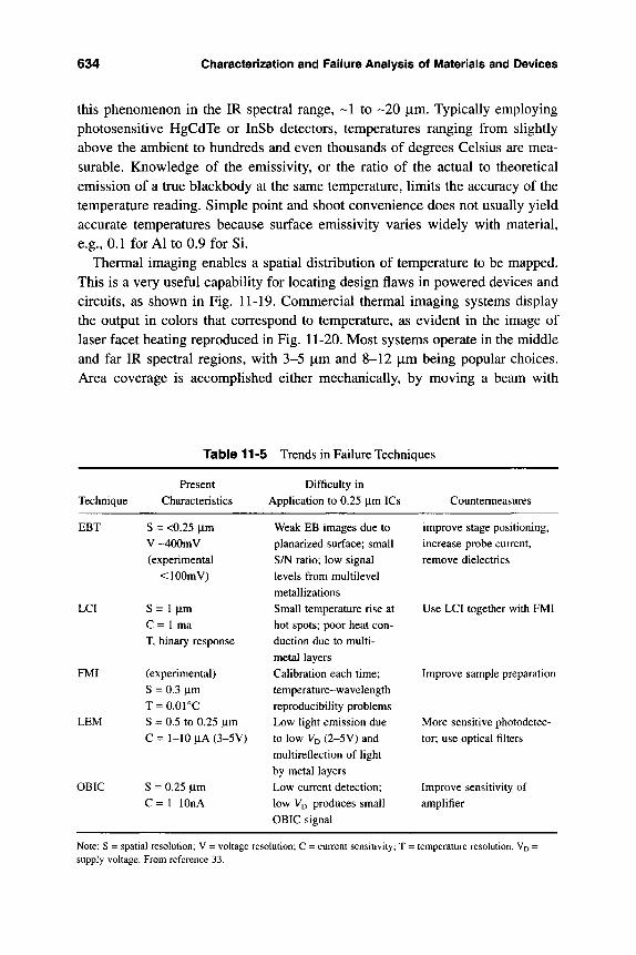
634 Characterization and Failure Analysis of Materials and Devices
this phenomenon in the IR spectral range, ~1 to -20 |im. Typically employing photosensitive HgCdTe or InSb detectors, temperatures ranging from slightly above the ambient to hundreds and even thousands of degrees Celsius are mea-surable. Knowledge of the emissivity, or the ratio of the actual to theoretical emission of a true blackbody at the same temperature, limits the accuracy of the temperature reading. Simple point and shoot convenience does not usually yield accurate temperatures because surface emissivity varies widely with material, e.g., 0.1 for Al to 0.9 for Si.
Thermal imaging enables a spatial distribution of temperature to be mapped. This is a very useful capability for locating design flaws in powered devices and circuits, as shown in Fig. 11-19. Commercial thermal imaging systems display the output in colors that correspond to temperature, as evident in the image of laser facet heating reproduced in Fig. 11-20. Most systems operate in the middle and far IR spectral regions, with 3-5 |xm and 8-12 |im being popular choices. Area coverage is accomplished either mechanically, by moving a beam with
Table 11-5 Trends in Failure Techniques
Technique Present
Characteristics Difficuhy in
Apphcation to 0.25 |xm ICs Countermeasures
EBT S = <0.25 |im V ~400mV (experimental
<100mV)
LCI S = 1 im C = 1 ma T, binary response
FMI (experimental) S = 0.3 |xm T = o.orc
LEM S = 0.5 to 0.25 |Lim C = 1-10 jLiA (3-5V)
OBIC S = 0.25 |Lim C = 1-lOnA
Weak EB images due to planarized surface; small S/N ratio; low signal levels from multilevel metallizations Small temperature rise at hot spots; poor heat con-duction due to multi-metal layers Calibration each time; temperature-wavelength reproducibility problems Low light emission due to low VD (2-5V) and multireflection of light by metal layers Low current detection; low VD produces small OBIC signal
improve stage positioning, increase probe current, remove dielectrics
Use LCI together with FMI
Improve sample preparation
More sensitive photodetec-tor; use optical filters
Improve sensitivity of amplifier
Note: S = spatial resolution; V = voltage resolution; C = current sensitivity; T = temperature resolution. Vp = supply voltage. From reference 33.
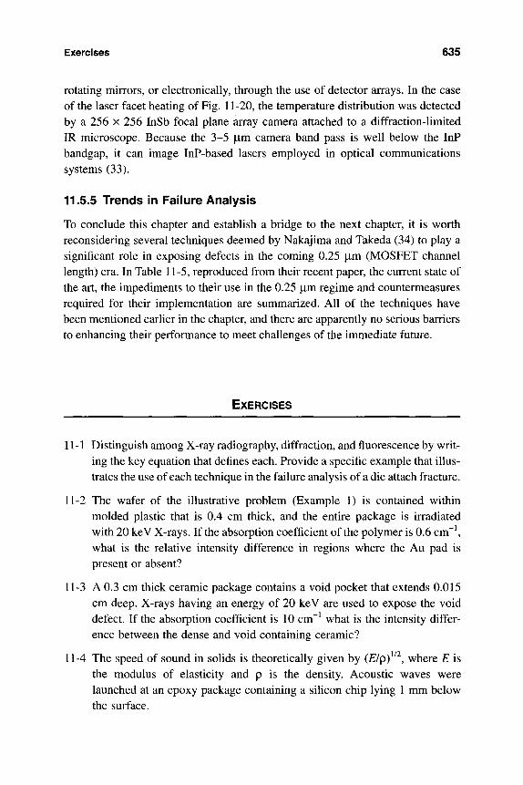
Exercises 635
rotating mirrors, or electronically, through the use of detector arrays. In the case of the laser facet heating of Fig. 11-20, the temperature distribution was detected by a 256 x 256 InSb focal plane array camera attached to a diffraction-limited IR microscope. Because the 3-5 |Lim camera band pass is well below the InP bandgap, it can image InP-based lasers employed in optical communications systems (33).
11.5.5 Trends in Failure Analysis
To conclude this chapter and establish a bridge to the next chapter, it is worth reconsidering several techniques deemed by Nakajima and Takeda (34) to play a significant role in exposing defects in the coming 0.25 |Lim (MOSFET channel length) era. In Table 11-5, reproduced from their recent paper, the current state of the art, the impediments to their use in the 0.25 |im regime and countermeasures required for their implementation are summarized. All of the techniques have been mentioned earlier in the chapter, and there are apparently no serious barriers to enhancing their performance to meet challenges of the immediate future.
EXERCISES
11-1 Distinguish among X-ray radiography, diffraction, and fluorescence by writ-ing the key equation that defines each. Provide a specific example that illus-trates the use of each technique in the failure analysis of a die attach fracture.
11-2 The wafer of the illustrative problem (Example 1) is contained within molded plastic that is 0.4 cm thick, and the entire package is irradiated with 20 keV X-rays. If the absorption coefficient of the polymer is 0.6 cm~\ what is the relative intensity difference in regions where the Au pad is present or absent?
11-3 A 0.3 cm thick ceramic package contains a void pocket that extends 0.015 cm deep. X-rays having an energy of 20 keV are used to expose the void defect. If the absorption coefficient is 10 cm~^ what is the intensity differ-ence between the dense and void containing ceramic?
11-4 The speed of sound in solids is theoretically given by {ElpY'^, where E is the modulus of elasticity and p is the density. Acoustic waves were launched at an epoxy package containing a silicon chip lying 1 nmi below the surface.
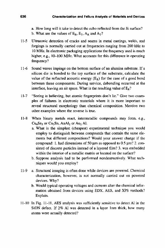
636 Characterization and Faiiure Anaiysis of i\Aateriais and Devices
a. How long will it take to detect the echo reflected from the Si surface? b. What are the values of ER, ET, AR and AT?
11-5 Ultrasonic detection of cracks and seams in metal castings, welds, and forgings is normally carried out at frequencies ranging from 200 kHz to 10 MHz. In electronic packaging applications the frequency used is much higher, e.g., 10-100 MHz. What accounts for this difference in operating frequency?
11-6 Sound waves impinge on the bottom surface of an alumina substrate. If a silicon die is bonded to the top surface of the substrate, calculate the value of the reflected acoustic energy (ER) for the case of a good bond between these components. During service, debonding occurred at the interface, leaving an air space. What is the resulting value of ER?
11-7 "Seeing is believing, but atomic fingerprints don't lie." Give two exam-ples of failures in electronic materials where it is more important to reveal structural morphology than chemical composition. Mention two other examples where the reverse is true.
11-8 When binary metals react, intermetallic compounds may form, e.g., Cu^Sns or CuaSn, AUAI2 or Au2 Al. a. What is the simplest (cheapest) experimental technique you would
employ to distinguish between compounds that contain the same ele-ments but different compositions? Would your answer change if the compound: 1. had dimensions of 50 lm as opposed to 0.5 |Lim? 2. con-sisted of discrete particles instead of a layered film? 3. was embedded within the interior of a metallic matrix or located on the surface?
b. Suppose analysis had to be performed nondestructively. What tech-niques would you employ?
11-9 a. Structural imaging is often done while devices are powered. Chemical characterization, however, is not normally carried out on powered devices. Why?
b. Would typical operating voltages and currents alter the chemical infor-mation obtained from devices using EDX, AES, and XPS methods? Explain.
11-10 In Fig. 11-11, AES analysis was sufficiently sensitive to detect Al in the SiON defect. If 2% Al was detected in a layer Inm thick, how many atoms were actually detected?
Exercises 637
11-11 For tungsten the core-electron energy levels in eV are given by:
K
69525
Li
12100
L2
11544
Ls
10207
Ml
2820
a. Create an energy level diagram for W. b. Calculate the energy and wavelength of the photon emitted when an
electron in a W atom falls from an « = 3 to the n = 1 state. c. A typical EDX detector system displays X-ray energies over a range of
1 to 30 keV. In performing an analysis on a Ti-W contact diffusion barrier, what are the energies of the X-rays that will be displayed?
11-12 Suggest ways to: 1. nondestructively examine the quality of the solder interconnections
between a flip-chip and ceramic substrate. 2. identify the nature of the discoloration on the surface of a passivated
IC chip. 3. nondestructively locate the exact position of a break in the grounding
strap within a 20 foot section of a buried telephone cable after it was dug up.
11-13 Consider a bipolar transistor which contains both ^ ^Sb and ^ ^Sb in the emitter but only ^ ^Sb in the collector. What does this information pro-vide on the doping processing methods employed?
11-14 Using liquid crystals on a 1.5 |im thick Si02 layer, a light spot 1 |im in diameter was observed to darken within 1 millisecond as the temperature rose 1°C. Approximately how much power was dissipated during the transition?
11-15 A coiled tungsten filament within an incandescent lamp is attached to copper-alloy lead wires. Failure occurred at the attachment interface. What analytical instruments would you use in order to determine the cause of failure?
11-16 a. Explain why the energy of oxide emission is greater than that for for-ward-bias bipolar light emission in Fig. 11-14.
b. In a p-n diode more light emission occurred under forward bias than negative bias. Why?
11-17 Thin film, foil, and ceramic capacitors undergo failures with often serious consequences. From what you know about them, suggest analysis tech-niques to study the following types of failures:
638 Characterization and Failure Analysis of Materials and Devices
1. pinholes in thin tantalum oxide film capacitors. 2. opens and shorts in wound tantalum and plastic foils used to make
capacitors. 3. voids in metal plates used to contact the dielectrics in ceramic capaci-
tors. 4. Delamination between alternating conductor and dielectric plates of
ceramic capacitors.
11-18 Carbon, wire-wound, and thin-film resistors undergo degradation that causes circuits to fail. From what you know about resistors suggest analy-sis techniques to study the following types of failures: 1. open wire-wound resistors due to fracture of the wires and broken
wire-end cap welds. 2. water absorption and electrostatic discharge of thin-film resistors.
11-19 Unstable transistor behavior and failure was observed in almost all of the chips of an experimental 1 Gb DRAM processed wafer. It is believed that contamination of gate oxides, which are 4.5 nm thick with 0.25 |xm lat-eral dimensions, occurred. In particular, transition metals at the Si-Si02 interface are suspected.
Suggest an experimental course of action in order to verify whether contamination was the root cause of failure, and recommend techniques and instruments necessary for such a study.
REFERENCES
1. G. Scheissler, C. Spivak, and S. Davidson, IEEE Proc. Custom Integrated Circuits Conf., p. 26.4.1 (1993).
2. C. R. Brundle, C. A. Evans, and S. Wilson, eds.. Encyclopedia of Materials Characterization, Butterworth-Heinemann, Boston (1992).
3. J. B. Bindell, in VLSI Technology, ed. S. M. Sze, McGraw Hill, New York (1988).
4. H. W. Werner, in Microelectronic Materials and Processes, ed. R. A. Levy, Kluwer, Dordrecht (1989).
5. E. S. Meieran, R A. Flinn, and J. R. Carruthers, Proc. IEEE, IS (7), 908 (1987). 6. T. M. Moore, Tutorial Notes, IEEE International Reliability Physics Sympo-
sium, 2cA (1992).
References 639
7. B. P. Richards and P. K. Footner, The Role of Microscopy in Semiconductor Failure Analysis, Oxford University Press, Oxford (1992).
8. P. Yalamanchili, A. Christou, S. Martel, and C. Rust, IEEE Circuits and Devices 10, 36, July (1994).
9. T. M. Moore, R. McKenna, and S. J. Kelsall, 29th Annual Proceedings of the IEEE Reliability Physics Symposium, p. 160 (1991).
10. N. Cartharge and V. Hauser, AT&T TechnolTech. Digest 68, 7 (1982). 11. W. Kern, R. B. Comizolli, and G. L. Schnable, RCA Review 43, 310 (1982). 12. D. R Field and D. J. Dingley, Solid State Technology 38 (11), 91 (1995). 13. K. L. Pey, W. K. Chim, J. C. H. Phang, and D. S. H. Chan, Microelectron-
ics and Reliability 34, 1193 (1994). 14. A. Rosencwaig, Ann. Rev. Mater Sci. 15, 103 (1985). 15. M. J. Li and M. Pecht, /. Electronic Packaging, Trans AIME 117, 225
(1995). 16. D. B. Williams and C. B. Carter, Transmission Electron Microscopy—A
Textbook for Materials Science, Plenum, New York (1996). 17. S. Morris, E. Tatti, E. Black, N. Dickson, H. Mendez, B. Schwiesow, and R.
Pyle, International Symposium on Testing and Failure Analysis, p. 417, Nov. (1991).
18. D. Briggs and M. P. Seah, eds.. Practical Surface Analysis by Auger and Photoelectron Spectroscopy, Wiley, New York (1984).
19. A. W. Benninghoven, F. G. Rudenauer, and H. W. Werner, Secondary Mass Ion Spectrometry—Basic Concepts, Instrumental Aspects, Applications and Trends, Wiley, New York (1987).
20. K. Evans, International Symposium on Testing and Failure Analysis, p. 45 (1989).
21. J. R. Bird and J. S. Williams, eds.. Ion Beams for Materials Analysis, Acad-emic Press, Sydney (1989).
22. M. Murase, NEC Res. & Develop. 35 (1), 52 (1994). 23. Y Uraoka, I. Miyanaga, K. Tsuji, and S. Akiyama, IEEE Trans. Semicon-
ductor Manuf 6 (4), 324 (1993). 24. J. Kolzer, A. Dallmann, G. Deboy, J. Otto, and D. Weinmann, Quality and
Reliability Engineering International 8, 225 (1992). 25. Y Uraoka, N. Tsutsu, Y Nakata, and S. Akiyama, IEEE Trans. Semicon-
ductor Manuf 4 (3), 183 (1991). 26. J. Mitsuhashi, S. Komori, and N. Tsubouchi, Quality and Reliability Engi-
neering International 8, 239 (1992). 27. K. S. Wills, C. J. Pilch, and A. Hyslop, 24th Annual Proceedings of the
IEEE Reliability Physics Symposium, p. 115 (1986).
640 Characterization and Failure Analysis of l\/laterials and Devices
28. T. C. May, G. L. Scott, E. S. Meieran, R Winer and V. R. Rao, 22nd Annual Proceedings of the IEEE Reliability Physics Symposium, p. 95 (1984).
29. K. J. Giewont, D. B. Hunt, and K. M. Hummler, J. Vac. Sci. Technol B 15 (4) 916 (1997).
30. C. G. C. de Kort, Philips Journal of Research 44, 2/3, 295 (1989). 31. F. Beck, Quality and Reliability Engineering International 2, 143 (1986). 32. B. Linnander, IEEE Circuits and Devices % 35, July (1993). 33. W-C.W. Fang, C. G. Bethea, Y. K. Chen, and S. L. Chuang, IEEE J. of
Selected Topics in Quantum Electronics 1, 117 (1995). 34. S. Nakajima and T. Takeda, Microelectronics and Reliability 37, 39 (1997).
Chapter 12
Future Directions and Reliability Issues
12.1 INTRODUCTION
In this final chapter, trends in semiconductor technology are projected into the future in order to assess the reliability issues that may arise in coming years. Pro-jections are always a risky business, so we may expect more speculative issues and subject matter to be raised here than elsewhere in the book. George San-tayana's famous admonition that "those who cannot remember the past are con-denmed to repeat it" has approximately applied to the reliability of microelec-tronics as well. Will the mind-boggling advances in semiconductor technology that have changed the world in so many ways continue unabated, with no sur-prises in store? If so, then we can profitably heed Santayana by projecting our current models of failure mechanisms to smaller feature sizes. However, what if history does not exactly repeat? Are there technological limits to how far device features can be shrunk? More fundaftientally, what are the physical limits to device behavior and feature sizes? Will the smaller devices and features spawn new failure mechanisms and reliability concerns? And finally, what strategies will have to be adopted to meet these future reliability challenges?
This chapter will attempt to address some of these difficult questions. Our roadmap into the future began in Chapter 1, where the kinds of electronic prod-ucts that are and will be in demand were considered. Here, feature scaling trends
641
642 Future Directions and Reliability Issues
in device processing will be projected into the future. Both considerations should provide a basis for assessing the growth in applications and capabilities of future electronic products. At some point, however, the apparently unbridled growth of microelectronics will eventually slow as some of the fundamental as well as practical size limitations are approached. The physical basis for these limits will, therefore, be discussed. We must however, temper these projections by what we have learned about failure and reliability in all of the intervening chapters. Lastly, the final section of the book addresses the subject of improving reliabil-ity and how to build it in.
12.2 INTEGRATED CIRCUIT TECHNOLOGY TRENDS
12.2.1 Introduction
To intelligently assess future reliability prospects we must first be sensitive to the implications of shrinking solid-state device dimensions. Our initial reaction, based on the content of previous chapters in this book, is probably to be skepti-cal or even pessimistic. After all, with smaller structures, atoms or electrons have shorter distances to traverse between "reliable" and "failed" states. This means that these states, the precursors to degradation and failure, will be accessed in shorter times. Happily, our intuition has proven wrong, and paradoxically, suc-cessive generations of integrated circuits have become increasingly more reli-able. The reasons for it are many and include improved electric-circuit designs, better materials, and cleaner, more controlled processing. Predictions of slow-downs in the dizzying pace of IC technology have not materialized; instead, market forces, competition, and human ingenuity have fostered the tenacious adherence to historical growth trends.
12.2.2 IC Chip Trends
Can feature reduction continue without limit and without incurring reliability penalties in devices? To address this question let us first examine Table 12-1 and Table 12-2, where near-term expected trends in IC technology and MOS devices are projected.
Accomplishing some of these projected goals will no doubt necessitate new technologies and materials. In DRAM capacitors, for example, oxide thickness limitations may necessitate the use of higher dielectric constant materials such as SrTiOs, PZT, or other ferroelectrics in order to maintain equivalent charge stor-age capabilities.
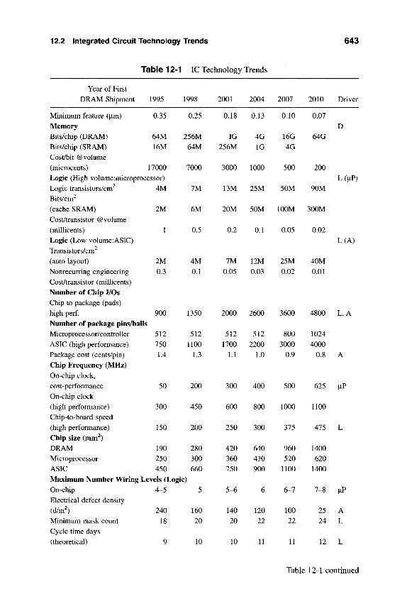
12.2 Integrated Circuit Technology Trends 643
Table 12-1 IC Technology Trends
Year of First DRAM Shipment
Minimum feature (|Lim) Memory Bits/chip (DRAM) Bits/chip (SRAM) Cost/bit ©volume (microcents)
1995
0.35
64M 16M
17000 Logic (High volume.microprocessor) Logic transistors/cm^ Bits/cm^ (cache SRAM) Cost/transistor ©volume (millicents) Logic (Low volumeiASlC) Transistors/cm^ (auto layout) Nonrecurring engineering Cost/transistor (millicents) Number of Chip I/Os Chip to package (pads) high perf.
4M
2M
1
2M 0.3
900 Number of package pins/balls Microprocessor/controller ASIC (high performance) Package cost (cents/pin) Chip Frequency (MHz) On-chip clock, cost-performance On-chip clock (high performance) Chip-to-board speed (high performance) Chip size (mm^) DRAM Microprocessor ASIC Maximum Number Wiring On-chip Electrical defect density (d/m^) Minimum mask count Cycle time days (theoretical)
512 750 1.4
50
300
150
190 250 450
1998
0.25
256M 64M
7000
7M
6M
0.5
4M 0.1
1350
512 1100
1.3
200
450
200
280 300 660
Levels (Logic) 4-5
240 18
9
5
160 20
10
2001
0.18
IG 256M
3000
13M
20M
0.2
7M 0.05
2000
512 1700
1.1
300
600
250
420 360 750
5-6
140 20
10
2004
0.13
4G IG
1000
25M
50M
0.1
12M 0.03
2600
512 2200
1.0
400
800
300
640 430 900
6
120 22
11
2007
0.10
16G 4G
500
50M
lOOM
0.05
25M 0.02
3600
800 3000
0.9
500
1000
375
960 520
1100
6-7
100 22
11
2010
0.07
64G
200
90M
300M
0.02
40M 0.01
4800
1024 4000
0.8
625
1100
475
1400 620
1400
7-8
25 24
12
Driver
D
L(^P)
L(A)
L,A
A
laP
L
|iP
A L
L
Table 12-1 continued
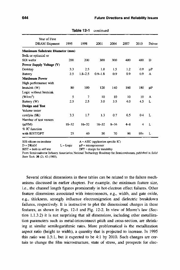
644 Future Directions and Reliability Issues
Table 12-1 continued
Year of First DRAM Shipment 1995
Maximum Substrate Diameter (mm) Bulk or epitaxial or SOI wafer Power Supply Voltage (V) Desktop Battery Maximum Power High performance with heatsink (W) Logic without heatsink (W/cm^) Battery (W) Design and Test Volume tester cost/pin ($K) Number of test vectors (^iP/M) % IC function with BIST/DFT
200
3.3 2.5
80
5 2.5
3.3
16-32
25
1998
200
2.5 1.8-2.5
100
7 2.5
1.7
16-32
40
2001
300
1.8 0.9-1.8
120
10 3.0
1.3
16-32
50
2004
300
1.5 0.9
140
10 3.5
0.7
8-16
70
2007
400
1.2 0.9
160
10 4.0
0.5
4-8
90
2010
400
0.9 0.9
180
10 4.5
0.4
4
90+
Driver
D
IP A
I P
A L
L
L
L
SOI-silicon-on-insulator A = ASIC (application specific IC) D = DRAM L = Logic |a.P = microprocessor BIST = built-in self test OFT = design for testability From Semiconductor Industry Association National Technology Roadmap for Semiconductors, published in Solid State Tech. 3S (2), 42 (1995).
Several critical dimensions in these tables can be related to the failure mech-anisms discussed in earlier chapters. For example, the minimum feature size, i.e., the channel length figures prominently in hot-electron effect failures. Other feature dimensions associated with interconnects, e.g., width, and gate oxide, e.g., thickness, strongly influence electromigration and dielectric breakdown failures, respectively. It is instructive to plot the dimensional changes in these features, as shown in Figs. 12-1 and Fig. 12-2. In view of Moore's law (Sec-tion 1.1.3.2) it is not surprising that all dimensions, including other metalHza-tion parameters such as metal-interconnect pitch and cross-section, are shrink-ing at similar semilogarithmic rates. More problematical is the metallization aspect ratio (height to width), a quantity that is projected to increase. In 1995 this ratio was 1.5:1, but it expected to be 4:1 by 2010. Such changes are cer-tain to change the film microstructure, state of stress, and prospects for elec-
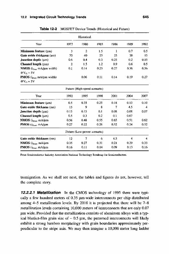
12.2 Integrated Circuit Technology Trends 645
Table 12-2 MOSFET Device Trends (Historical and Future)
Historical
Year
Minimum feature (|im) Gate oxide thickness (nm) Junction depth (|im) Channel length (|xm)
NMOS (iosat rnA/^im width) @VG = 5V PMOS (iosat mA/}im width) @VG = 5V
Year
Minimum feature (jim) Gate oxide thickness (nm) Junction depth (jim) Channel length (jim)
NMOS (/Dsat. mA/jim PMOS (iDsat. mA/jLim
1977
3 70
0.6 2
0.1
1980
2 40 0.4 1.5
0.14
0.06
Future (High-speed J
1992
0.5 15
0.15 0.5
0.56 0.27
1995
0.35 9
0.15 0.3
0.48 0.22
1983
1.5 25
0.3 1.2
0.23
0.11
scenario)
1998
0.25 8
0.1 0.2
0.55 0.26
1986
1 25
0.25 0.9
0.27
0.14
2001
0.18 7
0.08 0.1
0.65 0.32
1989
0.7 20
0.2 0.6
0.36
0.19
2004
0.13 4.5
0.08 0.07 0.51 0.24
1992
0.5 15
0.15 0.5
0.56
0.27
2007
0.10 4
0.07
0.62 0.32
Future (Low-power scenario)
Gate oxide thickness (nm)
NMOS (iDsat> mA/jim PMOS (iDsat* mA/fim
12 0.35 0.16
7 0.27 0.11
6 0.31 0.14
4.5 0.21 0.09
4 0.29 0.13
4 0.33 0.16
From Semiconductor Industry Association National Technology Roadmap for Semiconductors.
tromigration. As we shall see next, the tables and figures do not, however, tell the complete story.
12.2.2.1 Metallization In the CMOS technology of 1995 there were typi-cally a few hundred meters of 0.35 |im-wide interconnects per chip distributed among 4-5 metallization levels. By 2010 it is projected that there will be 7-8 metallization levels containing 10,000 meters of interconnects that are only 0.07 |xm wide. Provided that the metallization consists of aluminum alloys with a typ-ical blanket-film grain size of ~ 0.5 fim, the patterned interconnects will likely exhibit a strong bamboo morphology with grain boundaries approximately per-pendicular to the stripe axis. We may then imagine a 10,000 meter long ladder
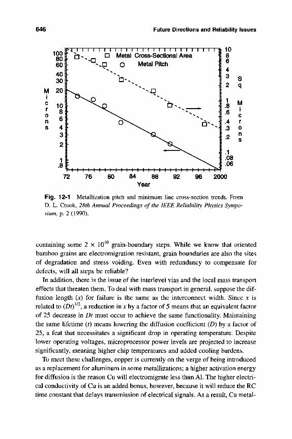
646 Future Directions and Reiiabiiity issues
4 I 1 I I I I I I I I I i I I I I I I I I I I [}x^ D Metal Cross-Sectional Area
.D O Metal Pitch
10 8 6 4 3 2
1 .8 .6 .4 .3
I .2
S q
M i c r 0 n s
.1
.08
.06
2000
Fig. 12-1 Metallization pitch and minimum line cross-section trends. From D. L. Crook, 28th Annual Proceedings of the IEEE Reliability Physics Sympo-sium, p. 2 (1990).
containing some 2 x 10 grain-boundary steps. While we know that oriented bamboo grains are electromigration resistant, grain boundaries are also the sites of degradation and stress voiding. Even with redundancy to compensate for defects, will all steps be reliable?
In addition, there is the issue of the interlevel vias and the local mass transport effects that threaten them. To deal with mass transport in general, suppose the dif-fusion length (x) for failure is the same as the interconnect width. Since x is related to {Dtf^, a reduction in x by a factor of 5 means that an equivalent factor of 25 decrease in Dt must occur to achieve the same functionality. Maintaining the same lifetime (0 means lowering the diffusion coefficient (D) by a factor of 25, a feat that necessitates a significant drop in operating temperature. Despite lower operating voltages, microprocessor power levels are projected to increase significantly, meaning higher chip temperatures and added cooling burdens.
To meet these challenges, copper is currently on the verge of being introduced as a replacement for aluminum in some metallizations; a higher activation energy for diffusion is the reason Cu will electromigrate less than Al. The higher electri-cal conductivity of Cu is an added bonus, however, because it will reduce the RC time constant that delays transmission of electrical signals. As a result, Cu metal-
12.2 Integrated Circuit Technology Trends 647
xriTTT—I—I 1 I—I—r~T—r~i—r~i—i—i—i—i—\—i i i \ i i r~r
* \
\ ( >
-" •
. s
20 i </) (fi CD
c ^^ - 10 o 8f 6 §
O
100 80
60
40
30
2000
Figs. 12-2 Gate oxide thickness and channel length. From D. L. Crook, 28th Annual Proceedings of the IEEE Reliability Physics Symposium, p. 2 (1990) and C. Hu Semi-conductor International, p. 105, June 1994.
lization is projected to increase circuit speed. Nevertheless, copper is difficult to plasma etch, and there are concerns that it can be a killer contaminant and poison silicon as well. There is an additional parallel strategy to increase chip speed, and that is to reduce circuit capacitance. For this reason there is an intense search for low-dielectric constant (e) insulators to replace the Si02 fill (£ = 3.9) that now sur-rounds the various levels of metallization. Assorted fluoropolymers (£ = -2.2 to ~3) as well as amorphous carbon (e = 2.6) have been touted for such use.
Metallization issues are only one example of the tradeoffs involved in imple-menting successive generations of devices and projecting their reliability. We have not even addressed processing complexities that an increase in the number of lithography steps implies. Lithography will have to cope with killer defects whose critical size decreases proportionately with feature geometry. For exam-ple, in 256 Mb DRAMs the killer-defect size is -0.02 jLim, but by 2010 it is pro-jected to be well below 10 nm.
648 Future Directions and Reliability Issues
12.2.2.2 Gate Oxide Hu (1) has pointed out two goals and two constraints associated with MOS scaHng and in particular, the influence of gate-oxide dimensions. The first goal is increased transistor current needed for quicker charging and discharging of parasitic capacitances. This requires short channels and high gate-oxide fields. To achieve the second goal, reduced sizes are required to increase device packing density, and minimize capacitance as well as power needs.
These two constraints demand suppression of leakage currents when the tran-sistor is off, and a typical reliability of 20 years. So called "short-channel" effects that lower the transistor threshold voltage and enhance bulk punch-through are causes of enhanced leakage currents. As with former generations of oxides, hot-carrier and contact-degradation effects as well as dielectric break-down will be the primary reliability concerns.
12.2.2.3 AC Versus DC Reliability Effects Inasmuch as Table 12-1 pro-jects a substantial increase in circuit operational frequencies, we may ask what effect this will have on the reliability of metallizations and gate oxides. A com-parison of mean times to failure obtained during both ac and dc testing has for-tunately revealed that the ratio MTTF(ac)/MTTF(dc) is substantially greater than one (2). This can be seen in Figs. 12-3a and b, where failure times are plotted versus frequency in the cases of electromigration and dielectric breakdown, respectively. The several orders of magnitude increase in interconnect lifetime relative to the dc value apparently stems from the inability to reach critical lev-els of defects; before vacancies can accumulate to generate void damage, the conductor heals because current reversal disperses them. Thus the ac signals that drive transistors will not cause damage; it is the larger bus lines that carry dc current that will pose the electromigration problems.
For analogous reasons, a 10-fold increase in gate-oxide life can be expected during ac relative to dc stressing. In this case holes do not have time to drift from the anode to the oxide interior because of field reversal. Instead of generating bulk electron traps that lead to breakdown, holes are limited to producing more benign interface traps.
Hu has also shown that the ac-to-dc hot-electron lifetime ratio for damage in n- as well as p-MOSFETs exceeds unity; however, the ratio decreases inversely with frequency increase.
12.2.3 Contamination Trends
Two major trends appear to define future contamination problems during chip processing. The first is the dominance of equipment and processes as sources of contamination relative to people and clean rooms. In the second, airborne mole-
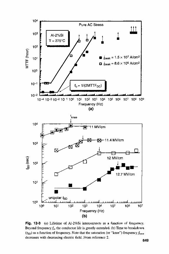
104
o
10-1 t
Pure AC Stress
i/i 1 m
• ypeak=1-5x10⁷A/cm2
D /peak = 8.6 X 10⁶ A/cm2
fo=1/(2MTTFDc)
10-4 10-3 10-2 10-1100 101 102 103 104 105 106 10^ 108 10^ Frequency (Hz)
(a)
ig -11 MV/cm
100 unipolar fsD
1 I NHIll 1 1 l l iml 1 I I mil l « ' «"iiil i i i mnl i i l u m l 11 HUH I I m i n i
100 101 102 103 104 105
Frequency (Hz)
(b)
106 107
Fig. 12-3 (a) Lifetime of Al-2%Si interconnects as a function of frequency. Beyond frequency/o, the conductor life is greatly extended, (b) Time to breakdown (%D) as a function of frequency. Note that the saturation (or "knee") frequency/knee decreases with decreasing electric field. From reference 2.
649
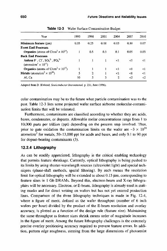
650 Future Directions and Reiiabiiity Issues
Table 12-3 Wafer Surface Contamination Budget
Year
Minimum feature (|im) Front End Processes
Organics (atoms of C/cm^ x 10 '*) Back End Processes
Anions F~, CI", S04^~, P04^" (atoms/cm^ x 10^ ) Organics (atoms of C/cm^ x 10^ )
Metals (atoms/cm^ x 10^ ) Al, Ca
1995
0.35
1
1
1 5
10
1998
0.25
0.5
1
1 2 5
2001
0.18
0.3
1
1 1 3
2004
0.13
0.1
<1
<1 <1
2
2007
0.10
0.05
<1
<1 <1 <2
2010
0.07
0.03
<1
<1 <1 <2
Adapted from D. Kinkead, Semiconductor International, p. 231, June (1996).
cular contamination may be to the future what particle contamination was to the past. Table 12-3 lists some projected wafer surface airborne molecular-contami-nation limits that will be tolerated.
Furthermore, contaminants are classified according to whether they are acids, bases, condensates, or dopants. Allowable molar concentrations range from 1 to 10,000 parts per trillion (ppt) depending on the process step involved. Thus, prior to gate oxidation the contamination limits on the wafer are ~3 x 10 ^ atoms/cm^ for metals, 50-13,000 ppt for acids and bases, and only 0.1 to 90 ppt for dopant-bearing contaminants (3).
12.2.4 Lithography
As can be readily appreciated, lithography is the critical enabling technology that permits feature shrinkage. Currently, optical lithography is being pushed to its limits by using shorter-wavelength sources (ultraviolet light) and special tech-niques (phase-shift methods, spatial filtering). By such means the resolution limit for optical lithography will be extended to about 0.15 jLim, corresponding to feature sizes in 1 Gb DRAMs. Beyond this, electron-beam and X-ray lithogra-phies will be necessary. Electron, or E-beam, lithography is already used in mak-ing masks and for direct writing on wafers but has not yet entered production lines. Comparison of the three lithography techniques is made in Fig. 12-4, where a figure of merit, defined as the wafer throughput (number of 6 inch wafers per hour) divided by the product of the E-beam resolution and overlay accuracy, is plotted as a function of the design rule (feature size). Maintaining the same throughput as feature sizes shrink means order of magnitude increases in the figure of merit. Among the future lithography challenges is the extremely precise overlay positioning accuracy required to prevent feature errors. In addi-tion, pattern edge roughness, steming from the large dimensions of photoresist
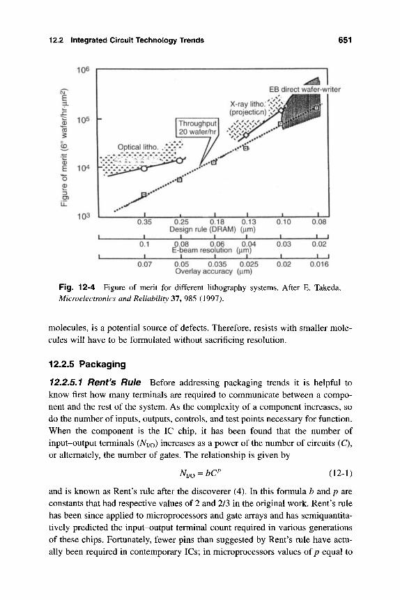
12.2 Integrated Circuit Technology Trends 651
106
0 E o 0)
-
EB direct wafer-writer E
^ 105 h 0
104 K
103 0.35 0.25 0.18 0.13
Design rule (DRAM) (jim) I I I I
0.10
0.1 0.08 0.06 0.04 E-beam resolution (|Lim)
0.03
0.07 0.05 0.035 0.025 Overlay accuracy (|Lim)
0.02
0.08
J I 0.02
- J I 0.016
Fig. 12-4 Figure of merit for different lithography systems. After E. Takeda, Microelectronics and Reliability 37, 985 (1997).
molecules, is a potential source of defects. Therefore, resists with smaller mole-cules will have to be formulated without sacrificing resolution.
12.2.5 Packaging
12.2.5.1 Rent's Rule Before addressing packaging trends it is helpful to know first how many terminals are required to communicate between a compo-nent and the rest of the system. As the complexity of a component increases, so do the number of inputs, outputs, controls, and test points necessary for function. When the component is the IC chip, it has been found that the number of input-output terminals (Nyo) increases as a power of the number of circuits (C), or alternately, the number of gates. The relationship is given by
Ny bCP (12-1)
and is known as Rent's rule after the discoverer (4). In this formula b and p are constants that had respective values of 2 and 2/3 in the original work. Rent's rule has been since applied to microprocessors and gate arrays and has semiquantita-tively predicted the input-output terminal count required in various generations of these chips. Fortunately, fewer pins than suggested by Rent's rule have actu-ally been required in contemporary ICs; in microprocessors values ofp equal to
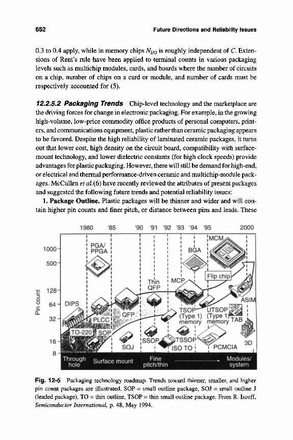
652 Future Directions and Reiiabllity Issues
0.3 to 0.4 apply, while in memory chips Nyo is roughly independent of C. Exten-sions of Rent's rule have been applied to terminal counts in various packaging levels such as multichip modules, cards, and boards where the number of circuits on a chip, number of chips on a card or module, and number of cards must be respectively accounted for (5).
12.2.5.2 Packaging Trends Chip-level technology and the marketplace are the driving forces for change in electronic packaging. For example, in the growing high-volume, low-price commodity office products of personal computers, print-ers, and communications equipment, plastic rather than ceramic packaging appears to be favored. Despite the high reliability of laminated ceramic packages, it turns out that lower cost, high density on the circuit board, compatibility with surface-mount technology, and lower dielectric constants (for high clock speeds) provide advantages for plastic packaging. However, there will still be demand for high-end, or electrical and thermal performance-driven ceramic and multichip-module pack-ages. McCullen et aH6) have recently reviewed the attributes of present packages and suggested the following future trends and potential reliability issues:
1. Package Outline. Plastic packages will be thinner and wider and will con-tain higher pin counts and finer pitch, or distance between pins and leads. These
'90 '91 '92 '93 '94 '95
Fig. 12-5 Packaging technology roadmap. Trends toward thinner, smaller, and higher pin count packages are illustrated. SOP = small outline package, SOJ = small outline J (leaded package), TO = thin outline, TSOP = thin small outline package. From R. Iscoff, Semiconductor International, p. 48, May 1994.
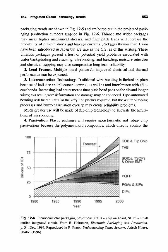
12.2 Integrated Circuit Technology Trends 653
packaging trends are shown in Fig. 12-5 and are borne out in the projected pack-aging production numbers graphed in Fig. 12-6. Thinner and wider packages may mean higher mechanical stresses, and finer pitch leads will increase the probability of pin-pin shorts and leakage currents. Packages thinner than 1 mm have been introduced in Japan but are rare in the U.S. as of this writing. These ultrathin packages present a host of potential yield problems associated with wafer backgrinding and cracking, wirebonding, and handling; moisture retention and chemical trapping may also compromise long-term reliability.
2. Lead Frames. Multiple metal planes for improved electrical and thermal performance can be expected.
3. Interconnection Technology. Traditional wire bonding is limited in pitch because of ball size and placement control, as well as tool interference with adja-cent bonds. Increasing lead count means finer pitch bond pads on the die and longer wires; as a result, wire deformation and damage may be enhanced. Tape-automated bonding will be required for the very fine pitches required, but the wafer bumping processes and bump-passivation overlap may create reliability problems.
Much greater use will be made of flip-chip technology to alleviate the limita-tions of wirebonding.
4. Passivation. Plastic packages will require more hermetic and robust chip passivations because the polymer mold compounds, which directly contact the
100
75 (0
O H—
o w 50 o m
25
Forecast
t /<;/<<^/,<^/,//|r/^/^/^^>^f/</^^<^</^/;/^/,4^/>^/\
-•«- jr ^^^
H 1980 1985 1990
Year 1995
COB & Flip Chip
TAB
SOICs, TSOPs & Other SMT
PQFP
PGAs & SIPs
DIPS
2000
Fig. 12-6 Semiconductor packaging projections. COB = chip on board, SOIC = small outline integrated circuit. From R. Heitmann, Electronic Packaging and Production, p. 34, Dec. 1993. Reproduced in R. Frank, Understanding Smart Sensors, Artech House, Boston (1996).
654 Future Directions and Reiiability issues
die, are not moisture barriers. The use of silicon nitride as the moisture barrier and polyimide for mechanical protection is one strategy; another approach employs reflowable glass/nitrides.
5. Die Attach. As die sizes increase there will probably be greater use made of the silver-filled epoxies. These evolve minimal amounts of volatile products on curing, thus inhibiting void formation. Voids are particularly troublesome during thermal cycling and are a cause of die fracture.
6. Circuit Board Mounting. Surface-mount technology will grow at the expense of through-hole mounting. In 1990 each of these solder mounting tech-nologies was employed equally, but by the end of the twentieth century surface mounting is projected to account for 95% of package attachments. This means that packages must be capable of resisting the solder reflow temperatures (~220°C). Fewer hygroscopic molding components will also be required. Pro-jecting into a future driven by increased numbers of I/O contacts and shrinking board space in which to accommodate them, flip-chip and ball-grid array mount-ing will become correspondingly favored. Micro ball-grid (|X-BGA) arrays with very small package footprints will no doubt gain wider acceptance.
In summary, the general trend is to more complex plastic/organic packages with larger dies using thinner and potentially more fragile passivations. These packages will have to withstand the thermomechanical shock of reflow solder-ing and the danger of popcorn cracking. They will also have to contend with higher temperatures as a result of increased microprocessor operating speeds. For example, newer versions of Pentium processors operating at frequencies greater than 200 MHz will generate twice the heat of chips they replace. Heat sinks or fans may be required, raising questions about battery life for portable applications. Package failure mechanisms and reliability problems that were raised in earlier chapters will remain concerns and probably worsen because of the added heat burden and increasing numbers of soldered electrical connec-tions.
12.3 SCALING
12.3.1 Introduction
Shrinking, or scaling down dimensions, is the usual route to improving device speed performance and approaching the reduced power-delay limits discussed in Section 12.4. The original device-scaling concept involved a coordinated change in dimensions, voltage, and doping while preserving a constant electric-field dis-
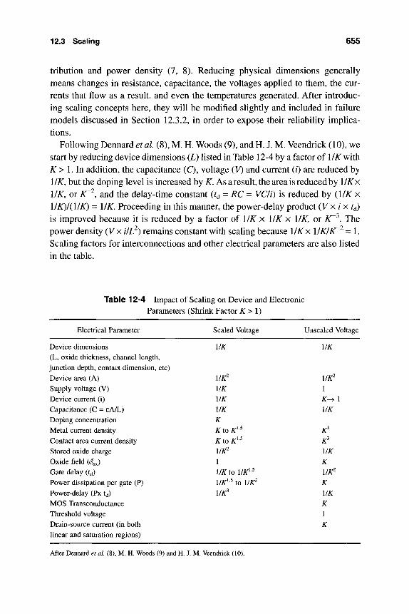
12.3 Scaling 655
tribution and power density (7, 8). Reducing physical dimensions generally means changes in resistance, capacitance, the voltages applied to them, the cur-rents that flow as a result, and even the temperatures generated. After introduc-ing scaling concepts here, they will be modified slightly and included in failure models discussed in Section 12.3.2, in order to expose their reliability implica-tions.
Following Dennard et al (8), M. H. Woods (9), and H. J. M. Veendrick (10), we start by reducing device dimensions (L) listed in Table 12-4 by a factor of 1/A with K> 1. In addition, the capacitance (C), voltage (V) and current (/) are reduced by \IK, but the doping level is increased by K. As a result, the area is reduced by 1/^x \IK, or K~^, and the delay-time constant (t^ = RC = VCIi) is reduced by {\IK x \IK)I{IIK) = \IK. Proceeding in this manner, the power-delay product (V x / x t^ is improved because it is reduced by a factor of 1/^ x 1/A x \IK, or K~^. The power density {Vxill}) remains constant with scaling because 1/^x IIKIKT^ = 1. Scaling factors for interconnections and other electrical parameters are also listed in the table.
Table 12-4 Impact of Scaling on Device and Electronic Parameters (Shrink Factor ^ > 1)
Electrical Parameter
Device dimensions (L, oxide thickness, channel length, junction depth, contact dimension, etc) Device area (A) Supply voltage (V) Device current (i) Capacitance (C = eA/L) Doping concentration Metal current density Contact area current density Stored oxide charge Oxide field ( 4 J Gate delay (tj) Power dissipation per gate (P) Power-delay (Px td) MOS Transconductance Threshold voltage Drain-source current (in both linear and saturation regions)
Scaled Voltage
l/K
l/K^ l/K l/K l/K K
KtoK'^ KtoK^^ l/K^ I l/K to l/K^-^ l/K^^ to l/K^ l/K^
Unsealed Voltage
l/K
l/K^ 1 K^ I l/K
K' K' l/K K l/K^ K l/K K I K
After Dennard et al. (8), M. H. Woods (9) and H. J. M. Veendrick (10).
656 Future Directions and Reliability Issues
In new generations of IC chips, the operating voltage is often not reduced, so that electric fields and power densities essentially increase. Assuming constant operating voltages, a different set of scaling factors is applicable, and these are entered in Table 12-4. Some scaling factors for MOSFETs under these condi-tions are also included. In what follows, the impact of scaling on several IC fail-ure mechanisms treated earlier in the book is considered.
12.3.2 Implications of Device Scaling
a. Electromigration The impact of scaling on electromigration reliability can be assessed by starting with the Black equation for the mean time to fail-ure (Eq. 5-31),
5 " e x p | ; MTTF = ^ r - ^ - (12-2)
It is assumed that B and E^ depend only on interconnect microstructure and not on scaling. For a worst-case, constant-voltage assumption, the current increases linearly, while cross-sectional dimensions decrease as the square of the scale factor; therefore, the current density scales as K^. But n = 2, so that an overall reduction in MTTF by a factor of K^ is predicted (11). Such a dis-astrous lifetime dependence on shrinking conductors is avoided by keeping j^ constant.
For contacts subjected to electromigration damage at thin sidewalls, the time-to-failure is given by a similar expression,
MTTF = - ^ ; ^ e x p ^ , (12-3)
where C is a constant independent of scaling, and L^ is proportional to the con-tact area. Because this area shrinks as K^, an overall decrease in lifetime by a factor of F^ may be anticipated. In both cases even higher scaling factors are possible if increased temperature operation is considered.
b. Oxide Breakdown Earlier, in Chapter 6, we considered both the recipro-cal-field and linear electric-field models for dielectric breakdown. With constant electric-field scaling there is no predicted adverse effect on reliability, because the expressions for MTTF under scaled (s) and unsealed (u) conditions are iden-tical. However, for the worst-case scenario of constant oxide voltage V^, the rec-iprocal field theory (Eq. 6-10) yields
12.3 Scaling 657
MTTF(s) MTTF(u) exp
^ R X O ( ^ - 1
(12-4)
where X^ is the oxide thickness and GR was defined earlier. In contrast, the lin-ear field model suggests that dielectric breakdown times are given by
MTTF(s)
MTTF(u) exp GL V, (K- 1)
Xo (12-5)
where GL was defined earlier, in Eq. 6-12. In either case, shrinkage of the gate-oxide thickness results in markedly shorter lifetimes. One consequence of scal-ing arises in screening. Weak oxides are normally screened through high-voltage stress for short time. As scaling has reduced oxide thicknesses, operating electric fields come closer to those for intrinsic wearout. This reduces field acceleration factors, making the screening of latent defects more difficult.
C. Hot-Carrier Effects We noted in Sect. 6.4.4 that the probability of inject-ing hot carriers from Si into Si02 is exponentially enhanced with increasing lat-eral electric field in the MOS channel. For short-channel lengths (Lc) the electric field varies inversely with L^. Hot-electron degradation thus scales in a manner similar to Eq. 12.4, or
MTTF(s)
MTTF(u) = exp
aU^-l
(12-6)
where a is a constant. Scaling down power-supply voltages is an obvious way to reduce the threat to reliability.
d. Soft Errors In Sect. 7.6.6.4 the critical charge (Qc) required to produce upsets was shown to decrease as device feature dimensions shrank (Eq. 7-46), thus enhancing the soft error rate (SER). Woods (11) has suggested that SER varies either exponentially or directly with Q^ for large or small charge levels, respectively. This would mean larger numbers of soft errors with respective scal-ing according to SER = exp (K^) or SER = K^.
Over the past 30 years a many-orders-of-magnitude decrease in reliability mar-gins has been predicted (Fig. 12-7) based on the effects of scaling devices and metallizations. Astonishingly, in apparent suspension of physical laws, the infant-mortality and long-term failure rates have actually declined. By the end of the twentieth century, a 10 FIT goal for ICs is projected. Perhaps when we take notice of the advances in the enabling processing technologies it is not so astonishing.
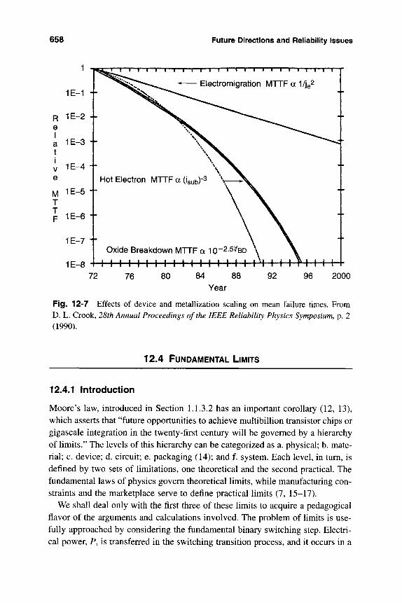
658 Future Directions and Reliabiiity Issues
1E-1 +
R 1E-2 I e I
1E-3 + t
V 1E-4 t e
M 1E-5 t T
I 1E-6 t
1E-7 t
1E-8
1—1111—I I I t I i I I I I 1 I I I I I 1 I I I
Electromigration MTTF a l/je^
Hot Electron MTTF a (isub)" \
Oxide Breakdown MTTF a 10~2-5^BD
I I I I I I I I I I M I I I I M 'I I I I y I I M 72 76 80 84 88
Year 92 96 2000
Fig. 12-7 Effects of device and metallization scaling on mean failure times. From D. L. Crook, 28th Annual Proceedings of the IEEE Reliability Physics Symposium, p. 2 (1990).
12.4 FUNDAI\/IENTAL LllVIITS
12.4.1 Introduction
Moore's law, introduced in Section 1.1.3.2 has an important corollary (12, 13), which asserts that "future opportunities to achieve multibillion transistor chips or gigascale integration in the twenty-first century will be governed by a hierarchy of limits." The levels of this hierarchy can be categorized as a. physical; b. mate-rial; c. device; d. circuit; e. packaging (14); and f. system. Each level, in turn, is defined by two sets of limitations, one theoretical and the second practical. The fundamental laws of physics govern theoretical limits, while manufacturing con-straints and the marketplace serve to define practical limits (7, 15-17).
We shall deal only with the first three of these limits to acquire a pedagogical flavor of the arguments and calculations involved. The problem of limits is use-fully approached by considering the fundamental binary switching step. Electri-cal power, P, is transferred in the switching transition process, and it occurs in a
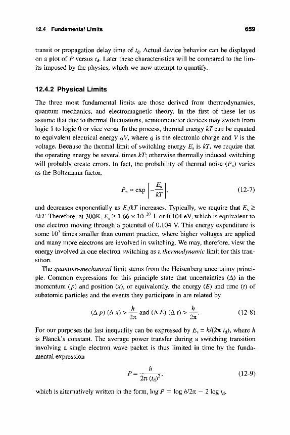
12.4 Fundamental Limits 659
transit or propagation delay time of t^. Actual device behavior can be displayed on a plot of P versus t^. Later these characteristics will be compared to the lim-its imposed by the physics, which we now attempt to quantify.
12.4.2 Physical Limits
The three most fundamental limits are those derived from thermodynamics, quantum mechanics, and electromagnetic theory. In the first of these let us assume that due to thermal fluctuations, semiconductor devices may switch from logic 1 to logic 0 or vice versa. In the process, thermal energy kT can be equated to equivalent electrical energy qV, where q is the electronic charge and V is the voltage. Because the thermal limit of switching energy E^ is kT, we require that the operating energy be several times kT; otherwise thermally induced switching will probably create errors. In fact, the probability of thermal noise (P^) varies as the Boltzmann factor.
^n - exp kT
(12-7)
and decreases exponentially as EJkT increases. Typically, we require that E^ > 4kT Therefore, at 300K, E, > 1.66 x 10"^^ J, or 0.104 eV, which is equivalent to one electron moving through a potential of 0.104 V. This energy expenditure is some 10^ times smaller than current practice, where higher voltages are applied and many more electrons are involved in switching. We may, therefore, view the energy involved in one electron switching as a thermodynamic limit for this tran-sition.
The quantum-mechanical limit stems from the Heisenberg uncertainty princi-ple. Common expressions for this principle state that uncertainties (A) in the momentum (p) and position (jc), or equivalently, the energy (E) and time (t) of subatomic particles and the events they participate in are related by
(A p) (Ax)>^ and (A ^ (A 0 > f". (12-8)
For our purposes the last inequality can be expressed by E^ = h/(2n t^), where h is Planck's constant. The average power transfer during a switching transition involving a single electron wave packet is thus limited in time by the funda-mental expression
which is alternatively written in the form, log P = log h/lrt — 2 log t^.
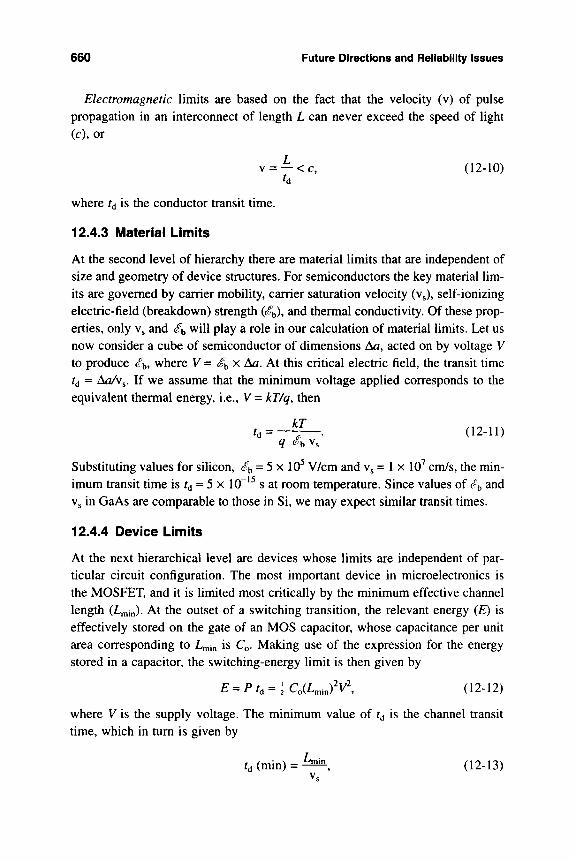
660 Future Directions and Reliability Issues
Electromagnetic limits are based on the fact that the velocity (v) of pulse propagation in an interconnect of length L can never exceed the speed of light (c), or
V = — < c, (12-10)
where t^ is the conductor transit time.
12.4.3 Material Limits
At the second level of hierarchy there are material limits that are independent of size and geometry of device structures. For semiconductors the key material lim-its are governed by carrier mobility, carrier saturation velocity (Vg), self-ionizing electric-field (breakdown) strength (^5), and thermal conductivity. Of these prop-erties, only Vs and ^b will play a role in our calculation of material limits. Let us now consider a cube of semiconductor of dimensions Aa, acted on by voltage V to produce b» where V= S'^x Aa. At this critical electric field, the transit time t^ = AoA^. If we assume that the minimum voltage applied corresponds to the equivalent thermal energy, i.e., V=kT/q, then
d = - f — . (12-11)
Substituting values for silicon, 4) = 5 x 10^ V/cm and Vs = 1 x 10^ cm/s, the min-imum transit time is t^- 5x 10" ^ s at room temperature. Since values of (4 and Vs in GaAs are comparable to those in Si, we may expect similar transit times.
12.4.4 Device Limits
At the next hierarchical level are devices whose limits are independent of par-ticular circuit configuration. The most important device in microelectronics is the MOSFET, and it is limited most critically by the minimum effective channel length (Lmin)- At the outset of a switching transition, the relevant energy (E) is effectively stored on the gate of an MOS capacitor, whose capacitance per unit area corresponding to L in is CQ. Making use of the expression for the energy stored in a capacitor, the switching-energy limit is then given by
E = Pt^ = \Co(L^jW\ (12-12)
where y is the supply voltage. The minimum value of t^ is the channel transit time, which in turn is given by
fd(min) = ^ (12-13)
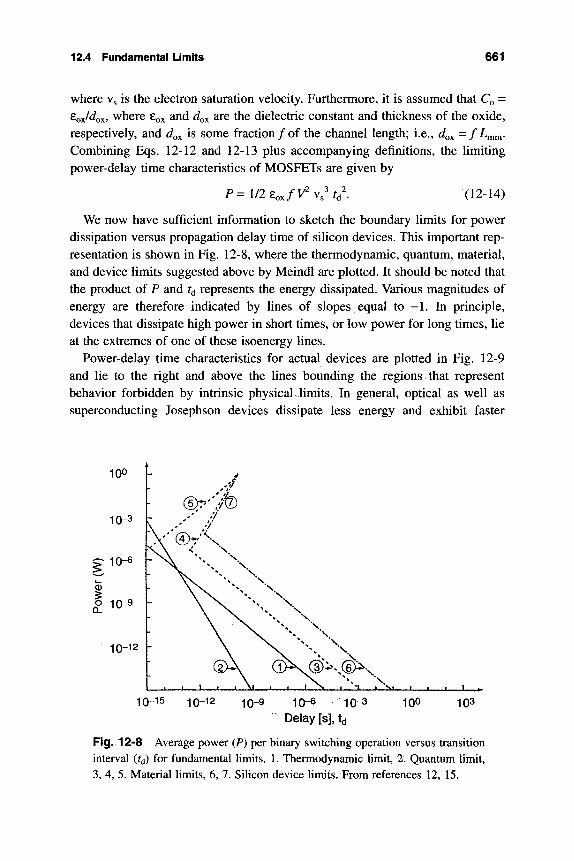
12.4 Fundamental Limits 661
where v is the electron saturation velocity. Furthermore, it is assumed that Q = 8ox/ ox» where Eox and d^^ are the dielectric constant and thickness of the oxide, respectively, and Jox is some fraction/of the channel length; i.e., ox =/^min-Combining Eqs. 12-12 and 12-13 plus accompanying definitions, the limiting power-delay time characteristics of MOSFETs are given by
P = l / 2 8, . / ^ ' V s ^ / (12-14)
We now have sufficient information to sketch the boundary limits for power dissipation versus propagation delay time of silicon devices. This important rep-resentation is shown in Fig. 12-8, where the thermodynamic, quantum, material, and device limits suggested above by Meindl are plotted. It should be noted that the product of P and t^ represents the energy dissipated. Various magnitudes of energy are therefore indicated by lines of slopes equal to - 1 . In principle, devices that dissipate high power in short times, or low power for long times, lie at the extremes of one of these isoenergy lines.
Power-delay time characteristics for actual devices are plotted in Fig. 12-9 and lie to the right and above the lines bounding the regions that represent behavior forbidden by intrinsic physical limits. In general, optical as well as superconducting Josephson devices dissipate less energy and exhibit faster
0 o a.
100
10-3
10-6
10-9
10-12
L
--. --
-
(^'
C'''(4>r''' \ V
-J 1 L-
.%'/ 'Vfe 7 '*\
N.
V \ N^ \ \ X ^ \
\ \ ^ \
\ ^ v ^^ \ .,-1 1 , »
10-15 10-12 10-9 10-6 10-3 Delay [s],td
100 103
Fig. 12-8 Average power (P) per binary switching operation versus transition interval {t^ for fundamental limits. 1. Thermodynamic limit, 2. Quantum limit, 3, 4, 5. Material limits, 6, 7. Silicon device limits. From references 12, 15.
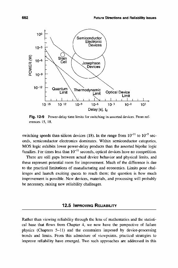
662 Future Directions and Reiiability issues
10-15 10-12 10-9 10-6 10-3 Delay [s], t^
Fig. 12-9 Power-delay time limits for switching in assorted devices. From ref-erences 15, 18.
switching speeds than silicon devices (18). In the range from 10" ^ to 10"^ sec-onds, semiconductor electronics dominates. Within semiconductor categories, MOS logic exhibits lower power-delay products than the assorted bipolar logic families. For times less than 10" ^ seconds, optical devices have no competition.
There are still gaps between actual device behavior and physical limits, and these represent potential room for improvement. Much of the difference is due to the practical limitations of manufacturing and economics. Limits pose chal-lenges and launch exciting quests to reach them; the question is how much improvement is possible. New devices, materials, and processing will probably be necessary, raising new reliability challenges.
12.5 liviPROviNG RELIABILITY
Rather than viewing reliability through the lens of mathematics and the statisti-cal base that flows from Chapter 4, we now have the perspective of failure physics (Chapters 5-11) and the constraints imposed by device-processing trends and limits. From this admixture of viewpoints, practical strategies to improve reliability have emerged. Two such approaches are addressed in this
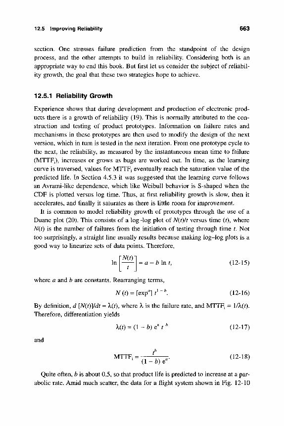
12.5 Improving Reliability 663
section. One stresses failure prediction from the standpoint of the design process, and the other attempts to build in reliability. Considering both is an appropriate way to end this book. But first let us consider the subject of reliabil-ity growth, the goal that these two strategies hope to achieve.
12.5.1 Reliability Growth
Experience shows that during development and production of electronic prod-ucts there is a growth of reliability (19). This is normally attributed to the con-struction and testing of product prototypes. Information on failure rates and mechanisms in these prototypes are then used to modify the design of the next version, which in turn is tested in the next iteration. From one prototype cycle to the next, the reliability, as measured by the instantaneous mean time to failure (MTTFi), increases or grows as bugs are worked out. In time, as the learning curve is traversed, values for MTTFi eventually reach the saturation value of the predicted life. In Section 4.5.3 it was suggested that the learning curve follows an Avrami-like dependence, which like Weibull behavior is S-shaped when the CDF is plotted versus log time. Thus, at first reliability growth is slow, then it accelerates, and finally it saturates as there is little room for improvement.
It is common to model reliability growth of prototypes through the use of a Duane plot (20). This consists of a log-log plot of N{t)lt versus time (0, where N{t) is the number of failures from the initiation of testing through time t. Not too surprisingly, a straight line usually results because making log-log plots is a good way to linearize sets of data points. Therefore,
In N{t)
a-bint, (12-15)
where a and b are constants. Rearranging terms,
A^(0 = [exp^] ^^"^ (12-16)
By definition, d [N(t)]/dt = X(t), where X is the failure rate, and MTTFi = l/A-(0-Therefore, differentiation yields
X(t) = (l-b) e f^ (12-17)
and
/*
Quite often, b is about 0.5, so that product life is predicted to increase at a par-abolic rate. Amid much scatter, the data for a flight system shown in Fig. 12-10
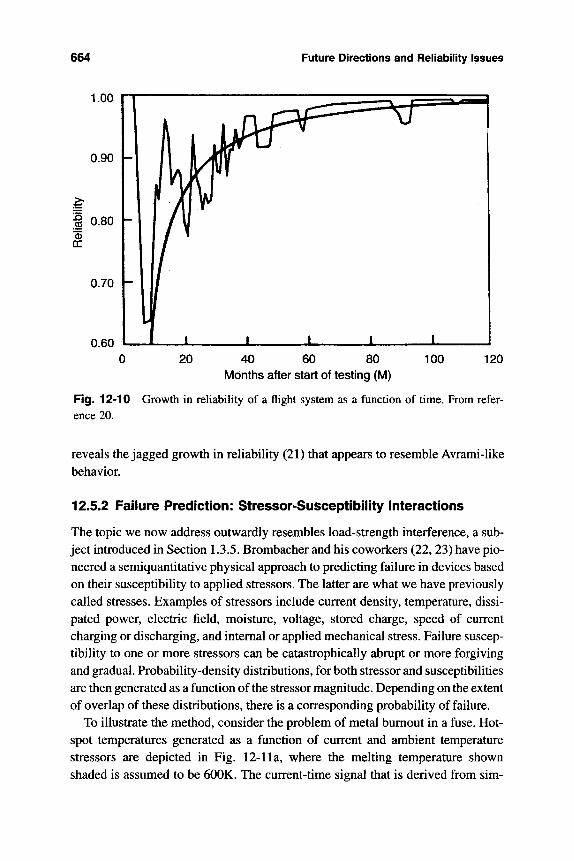
664 Future Directions and Reliability Issues
1.00
0.90
(D DC
0.70
0.60
r ± X
40 60 80 Mdnths after start of testing (M)
100 120
Fig. 12-10 Growth in reliability of a flight system as a function of time. From refer-ence 20.
reveals the jagged growth in reliability (21) that appears to resemble Avrami-like behavior.
12.5.2 Failure Prediction: Stressor-Susceptibility interactions
The topic we now address outwardly resembles load-strength interference, a sub-ject introduced in Section 1.3.5. Brombacher and his coworkers (22,23) have pio-neered a semiquantitative physical approach to predicting failure in devices based on their susceptibility to applied stressors. The latter are what we have previously called stresses. Examples of stressors include current density, temperature, dissi-pated power, electric field, moisture, voltage, stored charge, speed of current charging or discharging, and internal or applied mechanical stress. Failure suscep-tibility to one or more stressors can be catastrophically abrupt or more forgiving and gradual. Probability-density distributions, for both stressor and susceptibilities are then generated as a function of the stressor magnitude. Depending on the extent of overlap of these distributions, there is a corresponding probability of failure.
To illustrate the method, consider the problem of metal burnout in a fuse. Hot-spot temperatures generated as a function of current and ambient temperature stressors are depicted in Fig. 12-11 a, where the melting temperature shown shaded is assumed to be 600K. The current-time signal that is derived from sim-
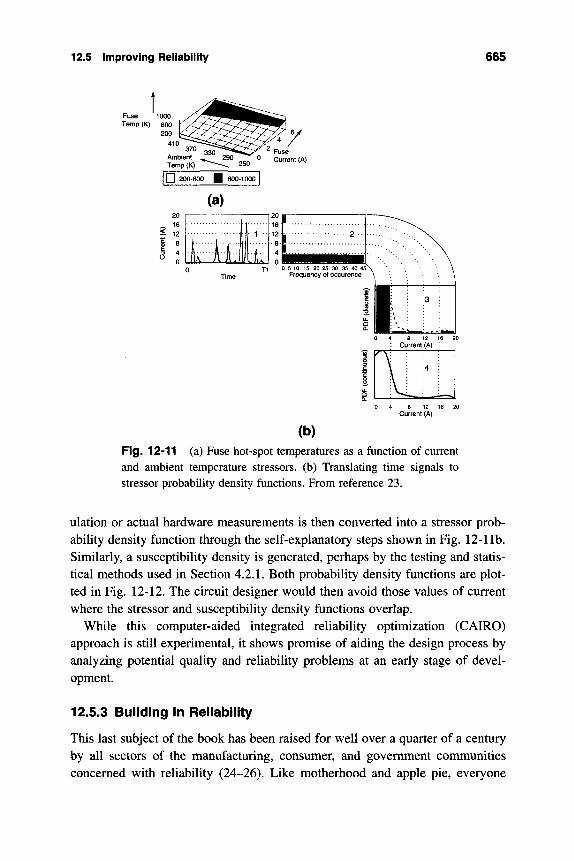
12.5 Improving Reliability 665
Fuse ^ Current (A)
Q 200-600 B 600-1000
< 2
i I
(a)
kill k 16 12-
::: 0
1
1 1 mmm
0 5 10 15 20 25 30 35 40 45^ Frequency of occurence
Current (A)
Current (A)
(b) Fig. 12-11 (a) Fuse hot-spot temperatures as a function of current and ambient temperature stressors, (b) Translating time signals to stressor probability density functions. From reference 23.
ulation or actual hardware measurements is then converted into a stressor prob-ability density function through the self-explanatory steps shown in Fig. 12-1 lb. Similarly, a susceptibility density is generated, perhaps by the testing and statis-tical methods used in Section 4.2.1. Both probability density functions are plot-ted in Fig. 12-12. The circuit designer would then avoid those values of current where the stressor and susceptibility density functions overlap.
While this computer-aided integrated reliability optimization (CAIRO) approach is still experimental, it shows promise of aiding the design process by analyzing potential quality and reliability problems at an early stage of devel-opment.
12.5.3 Building In Reliability
This last subject of the book has been raised for well over a quarter of a century by all sectors of the manufacturing, consumer, and government coromunities concerned with reliability (24-26). Like motherhood and apple pie, everyone
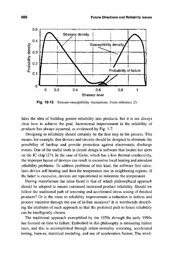
666 Future Directions and Reiiability Issues
0.4 0.6 Stressor level
Fig. 12-12 Stressor-susceptibility interactions. From reference 23.
likes the idea of building greater reliability into products, but it is not always clear how to achieve the goal. Incremental improvement in the reliability of products has always occurred, as evidenced by Fig. 1-7.
Designing in reliability should certainly be the first step in the process. This means, for example, that devices and circuits should be designed to eliminate the possibility of latchup and provide protection against electrostatic discharge events. One of the useful tools in circuit design is software that locates hot spots on the IC chip (27). In the case of GaAs, which has a low thermal conductivity, the improper layout of devices can result in excessive local heating and attendant reliability problems. To address problems of this kind, the software first calcu-lates device self-heating and then the temperature rise in neighboring regions. If the latter is excessive, devices are repositioned to minimize the temperature.
During manufacture the issue faced is that of which philosophical approach should be adopted to ensure continued increased product reliability. Should we follow the traditional path of screening and accelerated stress testing of finished products? Or is the route to reliability improvement a reduction in defects and process variation through the use of in-line monitors? It is worthwhile describ-ing the attributes of each approach so that the preferred path to future reliability can be intelligently chosen.
The traditional approach exemplified by the 1970s through the early 1990s has focused on time to failure. Embodied in this philosophy is measuring failure rates, and this is accomplished through infant-mortality screening, accelerated testing, bum-in, statistical modeling, and use of acceleration factors. The mind-
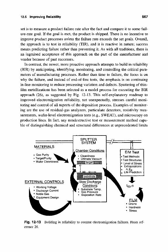
12.5 Improving Reliability 667
set is to measure a product failure rate after the fact and compare it to some fail-ure-rate goal. If the goal is met, the product is shipped. There is no incentive to improve product processes unless the failure rate exceeds the set goals. Overall, the approach is to test in reliability (TIR), and it is reactive in nature; success means predicting failure rather than preventing it. As with all traditions, there is an ingrained acceptance of this approach on the part of the manufacturer and vendor because of past successes.
In contrast, the newer, more proactive approach attempts to build in reliability (BIR) by anticipating, identifying, monitoring, and controlling the critical para-meters of manufacturing processes. Rather than time to failure, the focus is on why the failure, and instead of end-of-line tests, the emphasis is on continuing in-line monitoring to reduce processing variation and defects. Sputtering of thin-film metallizations has been selected as a model process for executing the BIR approach (26), as suggested by Fig. 12-13. This self-explanatory roadmap to improved electromigration reliability, not unexpectedly, stresses careful moni-toring and control of all aspects of the deposition process. Examples of monitor-ing are the use of residual-gas analyzers, particulate detectors, resistivity mea-surements, wafer-level electromigration tests (e.g., SWEAT), and microscopy on production lines. In fact, any nondestructive test or measurement method capa-ble of distinguishing chemical and structural differences at unprecedented limits
MATERIALS
• Gas Purity • Target/Purity • Wafer Cleanliness"
EXTERNAL CONTROLS • Working Voltage • Discharge Current • Noble Gas
L^ Equipment Design
SPUTTER SYSTEM
E/M Test • Test Methods • Test Structures • Level of Stress • Extrapolations • n,Ee • Life Prediction
Fig. 12-13 Building in reliability to counter electromigration failures. From ref-erence 26.
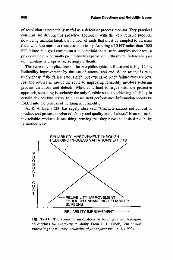
668 Future Directions and Reiiabiiity Issues
of resolution is potentially useful as a defect or process monitor. Very practical concerns are driving this proactive approach. With the very reliable products now being manufactured, the number of units that must be sampled to measure the low failure rates has risen astronomically. Assuring a 10 FIT rather than 1000 FIT failure-rate goal may mean a hundredfold increase in samples under test, a procedure that is normally prohibitively expensive. Furthermore, failure analysis on high-density chips is increasingly difficult.
The economic implications of the two philosophies is illustrated in Fig. 12-14. Reliability improvement by the use of screens and end-of-line testing is rela-tively cheap if the failure rate is high, but expensive when failure rates are low. Just the reverse is true if the route to improving reliability involves reducing process variations and defects. While it is hard to argue with the proactive approach, screening is probably the only feasible route to achieving reliability in certain devices like lasers. In all cases field performance information should be folded into the process of building in reliability.
As R. A. Evans (28) has sagely observed, "Characterization and control of product and process is what reliability and quality are all about." Even so, mak-ing reliable products is one thing; proving that they have the desired reliability is another issue.
P R O D U C T
C O
s T
RELIABILITY IMPROVEMENT THROUGH REDUCING PROCESS VARIATION/DEFECTS
-RELIABILITY IMPROVEMENT THROUGH ENHANCING RELIABILITY SCREENS
RELIABILITY IMPROVEMENT
Fig. 12-14 The economic implications of building-in and testing-in philosophies for improving reliability. From D. L. Crook, 28th Annual Proceedings of the IEEE Reliability Physics Symposium, p. 2, (1990)
Exercises 669
EXERCISES
12-1 What average rate of annual increase in transistor count has occurred over the 40 years from 1957 to 1997?
12-2 The Semiconductor Industry Association roadmap for silicon wafers includes the following projections:
Year 1995 1998 2001 2004 2007 2010
Minimum feature (fxm) Wafer diameter (mm) Surface Fe, Ni, Cu, Zn, Na (10^^ at/cm^) Total bulk Fe (10^^ at/cm^) Oxygen (ppma) Bulk microdefects (def/cm^) Oxygen-induced stacking faults (def/cm^) Particles per unit area (#/m^)
0.35 200
5 1
24 5000 20
1700
0.25 200 2.5 0.5 23
1000 20
1300
0.18 300
1 0.2 23
500 5
750
0.13 300 0.5 0.1 22 100 1
550
0.10 400 0.25 0.05 22 100 1
275
0.07 400
TBD TED TBD 100 1
150
a. What accounts for the roughly constant projected oxygen concentra-tion?
b. Why is it important to minimize the presence of the transition metals? c. If the oxygen concentration remains constant, what factors will serve
to reduce the bulk microdefect and oxygen-induced stacking fault densities?
d. Suppose microprocessor chips have the same killer-defect densities as noted above. Predict whether yields for these chips will increase or decrease with time from 1995 to 2010.
12-3 The memory-cell area of DRAMs has declined exponentially with time; e.g, 34 [im^, 1Mb in 1985; 1.6 |im^ 64 Mb in 1994; and 0.6 |im^ 256 Mb in 1997. Concurrently, the DRAM die area has increased at a greater than linear rate; e.g., 60 mm^ in 1985; 200 mm^ in 1994; and 300 mm^ in 1997. Plot these trends as a function of time. Explain the variation in die size with time.
12-4 How do you explain the paradox of decreasing reliability margins with scaling and a decreasing failure rate of ICs?
12-5 Show by means of sketches that as device densities and number of pads increase and package dimensions shrink, the length of bond wires must increase.
670 Future Directions and Reliability Issues
12-6 The total number of pins on the Pentium Pro (P6) microprocessor is 387 instead of the 900 predicted by an overly conservative version of Rent's rule. If each pin is 99.99% reliable, what is the relative difference in reli-ability between these two pin counts?
12-7 Suppose the failure rate of the fight system in Fig. 12-10 is given by A.(t) = 0.5 (exp a)i^'\ a. Derive an expression for the reliability dependence on time. b. From the reUability function and Fig. 12-10 calculate the value of a.
12-8 Develop a formula for the dependence of Al-2%Cu interconnect life on ac frequency and current density using data plotted in Fig. 12-3a. Does the low-frequency MTTF data obey the Black-equation dependence on current density?
12-9 Consider the dependence of oxide-breakdown times on frequency shown in Fig. 12-3b. a. Which model—the reciprocal electric-field or linear electric-field—
better describes breakdown times at a frequency of 1 Hz? b. Which model—the reciprocal electric-field or linear electric-field—
better describes breakdown times at a frequency of 10^ Hz? c. Can you account for the decrease in saturation (knee) frequency with
decreasing electric field?
12-10 Sketch the cross-sectional view of a field-effect transistor, e.g.. Fig. 2-16a, with source and drain contact metals in place. Resketch the tran-sistor dimensions under constant-field scaling conditions where features are reduced by a constant factor.
12-11 The MOS transistor gate-oxide thickness and voltage are projected to be 4 nm and 0.9 V, respectively, in 2007. Under these conditions the elec-tron tunneling current density through the oxide has been measured to be roughly 10"^ A/cm^. Speculate on the implications of the above with respect to the reliability of such gate oxides.
12-12 Suppose a CMOS device whose features are 0.1 \xm in size switches with energies of 5 x 10" ^ J. Locate the position of this device on Fig. 12-9.
12-13 There are important needs for new dielectric materials for use in DRAM storage capacitors and as inter-(metallization) layer filling, a. In each case explain whether a higher or lower dielectric constant
material, relative to that currently used, is desired.
References 671
b. Corrosion of Al-Cu metallization in contact with dielectrics is a potential reliability problem. How would you predict whether particu-lar metallization-dielectric pairs are reactive? What can be done to prevent reaction?
REFERENCES
1. C. Hu, Semiconductor International, p. 105 June (1994). 2. C. Hu, Microelectronics and Reliability 16, 1611 (1996). 3. D. Kinkead, Semiconductor International, p. 231, June (1996). 4. C. Radke, IEEE Proc. Design Automation Conf., 257 (1969). 5. D. P. Seraphim and A. L. Jones, in Principles of Electronic Packaging, ed.
D. P. Seraphim, R. Lasky, and C.-Y. Li, McGraw-Hill, New York (1989). 6. J. McCullen, T. M. Moore and S. V. Golwalker, Tutorial Notes, IEEE Inter-
national Reliability Physics Symposium, 1,1 (1996). 7. V. L. Rideout, in VLSI Electronics Microstructure Science, Vol 7, ed. N. Ein-
spruch, Academic Press, Orlando (1983). 8. R. H. Dennard, F. H. Gaensslen, H. N. Yu, V. L. Rideout, E. Bassous, and A.
LeBlanc, IEEE J. Solid State Circuits, SC-9, 256 (1974). 9. M. H. Woods, Prac. IEEE, 74 (12), 1715 (1986).
10. H. J. M. Veendrick, MOS ICs-From Basics to ASICs, VCH PubHshers, Weinheim (1992).
11. M. H. Woods, IEEE Tutorial Notes, IEEE International Reliability Physics Symposium, 6.1 (1985).
12. J. D. Meindl, Pwc. IEEE 83 (4) 619 (1995). 13. J. D. Meindl, J. Vac. ScL Tech. 14, 192 (1996). 14. W. E. Pence and J. P. Krusius, IEEE Trans. Comp. Hybrids and Manuf.
Tech. 10 (2), 176 (1987) 15. J. D. Meindl, Circuits and Devices, 12, 19, Nov. (1996). 16. R. W. Keyes, Advances in Electronics Physics 70, 159 (1988). 17. S. J. Wind, D. J. Frank and H.-S. Hong, Microelectronic Engineering 32,
271(1996). 18. P W. Smith, IEEE Circuits and Devices 3, 9, May (1987). 19. H. S. Blanks, Microelectronics and Reliability 20, 219 (1980). 20. J. J. Duane, IEEE Trans, on Aerospace 2, 563 (1964). 21. D. J. Lloyd, Quality and Reliability Engineering International 2, 19 (1986).
672 Future Directions and Reiiabiiity Issues
22. A. C. Brombacher, Reliability by Design, CAE Techniques for Electronic Components and Systems, Wiley, Chichester (1992).
23. A. C. Brombacher, E. V. Geest, R. Arendsen, A. V. Steenwuk, and O. Herr-mann, Quality and Reliability Engineering International 9, 239 (1993).
24. W. H. Schroen, J. G. Aiken, and G. A. Brown, 10th Annual Proceedings of the IEEE Reliability Physics Symposium, p. 42 (1972).
25. H. A. Schafft, D. A. Baglee, and P. E. Kennedy, 29th Annual Proceedings of the IEEE Reliability Physics Symposium, p. 1 (1991).
26. D. L. Erhart, H. A. Schafft, and W. K. Gladden, IEEE International Inte-grated Reliability Workshop, Lake Tahoe, Oct. (1995).
27. T. Volden and J. Hootman, Circuits and Devices 11, 23, Sept. (1995). 28. R. A. Evans, IEEE Trans, on Reliability 42 (4), 541 (1993).
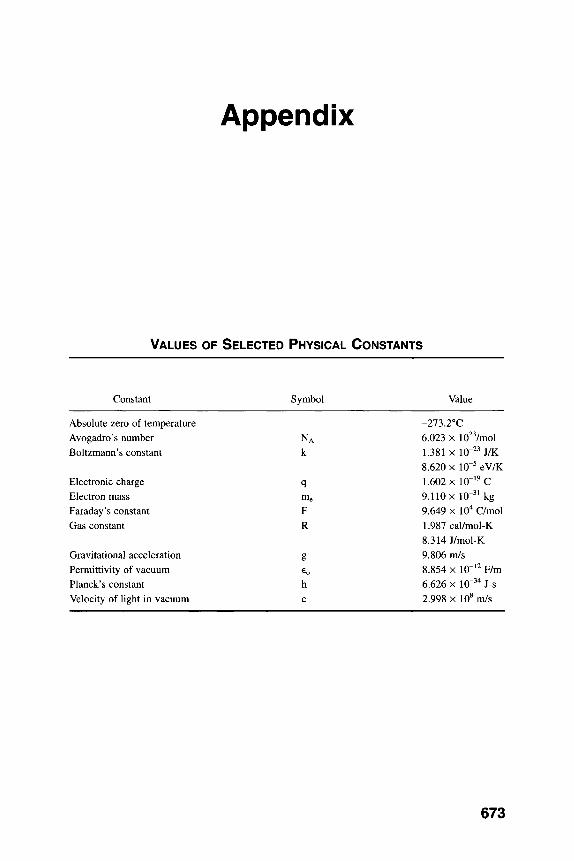
Appendix
VALUES OF SELECTED PHYSICAL CONSTANTS
Constant Symbol Value
Absolute zero of temperature Avogadro's number Boltzmann's constant
Electronic charge Electron mass Faraday's constant Gas constant
Gravitational acceleration Permittivity of vacuum Planck's constant Velocity of light in vacuum
NA
k
q me F R
g Co
h c
-273.2°C 6.023 X lO^Vmol 1.381 X 10"^^ J/K 8.620 X 10"^ eV/K 1.602 X 10"^^ C 9.110 X 10" ^ kg 9.649 X 10^ C/mol 1.987 cal/mol-K 8.314 J/mol-K 9.806 m/s 8.854 X 10"^^ F/m 6.626 X 10"^^ J-s 2.998 X 10^ m/s
673

This Page Intentionally Left Blank
Index
Abrasive wear, 488 Accelerated corrosion testing, 375-376 Accelerated current cycling tests, 489 Accelerated stress-cycling testing, 516 Accelerated temperature-humidity-ionic conta-
mination testing, 381 Acceleration factor (AF), 24-25, 212-214, 225.
See also Arrhenius acceleration factor; Linear acceleration factors; Solder; True acceleration factors; Voltage accelera-tion factors.
Accumulation, 63 Acoustic imaging, 596 Acoustic impedance, 597 Acoustic microscopy, 598 Acoustic waves, 595 Activation energies, 213, 214, 224, 225, 245,
268, 274, 308, 577. See also Stress-reduced activation energy.
Activation free energy, 20 Activation-energy values, 497 Adhesion force, 147 Adhesive wear, 488 Advisory Group on Reliability of Electronic
Equipment (AGREE), 15 Aerodynamic drag, 151 AES, 615, 617-618 Age softening, 437 Ag-fiUed epoxies, 420 Airborne contamination sources, 360-363 Al alloy metallizations, 278, 376 Al interconnect, 270, 275 Al-Cu precipitation hardening alloys, 279 AlGaAs lasers, 90, 540 AlGaAs/GaAs heterostructures, 540 Alkah ion contaminants, 70 Alloy spiking, 347 Alpha particles, 394, 401 Al-Si phase diagram, 250 Aluminum-Silicon (Al-Si) contacts, 248-252 Anodic polarization, 370 Anomalous dopant-diffusion effects, 110
Antenna ratio-dependent damage, 325 Antisite defects, 109 APDs. See Avalanche photodiodes. Application-specific ICs (ASICs), 5 Arcing, 51 Arrhenius, 20, 25, 214-215, 218-219, 321
acceleration factor, 219 Asperities, 479, 492 Atmospheric contamination, 359, 360-366 Atom movements, 20-24, 480. See also Solids. Atom transport. See Electromigration; Stresses. Atomic diffusion, 18, 21, 238 Atomic displacement, 393-395 Atomic fluorescent X-rays, 605 Atomic force microscope (AFM), 578, 581,
604, 605 Atomic velocities, 23 Au-based gate metallizations, 256 Au-Cr ohmic contact metallization, 274 Auger electrons, 395, 618
spectrometer, 607 Au-Si eutectic alloy solder, 418 AvailabiHty, 17 Avrami equation, 209-211, 663
B Backscattered electron-diffraction pattern, 280 Backscattered electrons, 607 Backscattered ions, 620 Ball grid array(s) (BGA), 449, 462, 593, 654 Ball limited metallurgy (BLM), 426, 427
interface, 444 Ball-wire interface, 422 Bamboo grain structure, 289 Band diagrams, 46 Band-gap energy, 48 Base current gain, 60 Basquin's exponent, 500 Bathtub curve, 29-31, 219-222 Bathtub failure, 29-31 Beam deflection, 136, 484 Beams, 528-529 Biaxial stress distribution, 286
675
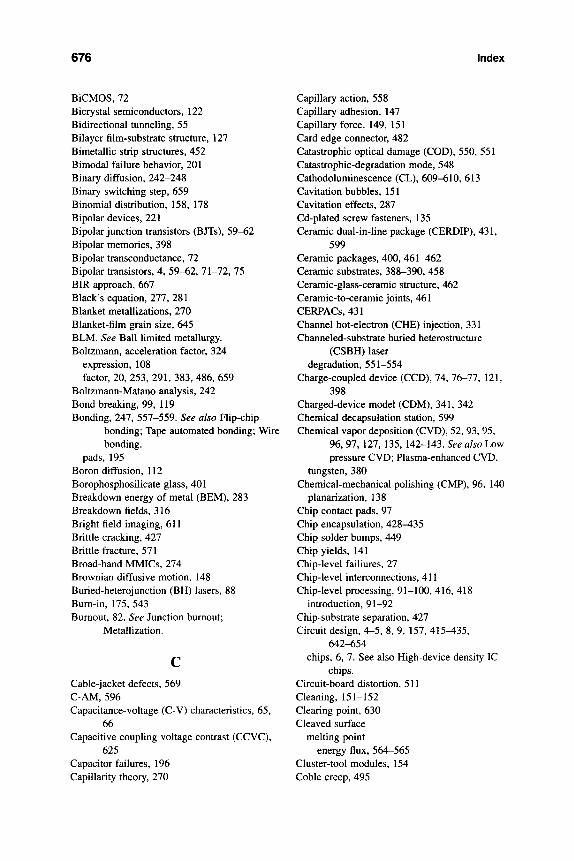
676 Index
BiCMOS, 72 Bicrystal semiconductors, 122 Bidirectional tunneling, 55 Bilayer film-substrate structure, 127 Bimetallic strip structures, 452 Bimodal failure behavior, 201 Binary diffusion, 242-248 Binary switching step, 659 Binomial distribution, 158, 178 Bipolar devices, 221 Bipolar junction transistors (BJTs), 59-62 Bipolar memories, 398 Bipolar transconductance, 72 Bipolar transistors, 4, 59-62, 71-72, 75 BIR approach, 667 Black's equation, 277, 281 Blanket metallizations, 270 Blanket-film grain size, 645 BLM. See Ball limited metallurgy. Boltzmann, acceleration factor, 324
expression, 108 factor, 20, 253, 291, 383, 486, 659
Boltzmann-Matano analysis, 242 Bond breaking, 99, 119 Bonding, 247, 557-559. See also Flip-chip
bonding; Tape automated bonding; Wire bonding.
pads, 195 Boron diffusion, 112 Borophosphosilicate glass, 401 Breakdown energy of metal (BEM), 283 Breakdown fields, 316 Bright field imaging, 611 Brittle cracking, 427 Brittle fracture, 571 Broad-band MMICs, 274 Brownian diffusive motion, 148 Buried-heterojunction (BH) lasers, 88 Bum-in, 175, 543 Burnout, 82. See Junction burnout;
Metallization.
Cable-jacket defects, 569 C-AM, 596 Capacitance-voltage (C-V) characteristics, 65,
66 Capacitive coupling voltage contrast (CCVC),
625 Capacitor failures, 196 Capillarity theory, 270
Capillary action, 558 Capillary adhesion, 147 Capillary force, 149, 151 Card edge connector, 482 Catastrophic optical damage (COD), 550, 551 Catastrophic-degradation mode, 548 Cathodoluminescence (CL), 609-610, 613 Cavitation bubbles, 151 Cavitation effects, 287 Cd-plated screw fasteners, 135 Ceramic dual-in-line package (CERDIP), 431,
599 Ceramic packages, 400, 461-462 Ceramic substrates, 388-390, 458 Ceramic-glass-ceramic structure, 462 Ceramic-to-ceramic joints, 461 CERPACs, 431 Channel hot-electron (CHE) injection, 331 Channeled-substrate buried heterostructure
(CSBH) laser degradation, 551-554
Charge-coupled device (CCD), 74, 76-77, 121, 398
Charged-device model (CDM), 341, 342 Chemical decapsulation station, 599 Chemical vapor deposition (CVD), 52, 93, 95,
96, 97, 127, 135, 142-143. See also Low pressure CVD; Plasma-enhanced CVD.
tungsten, 380 Chemical-mechanical polishing (CMP), 96, 140
planarization, 138 Chip contact pads, 97 Chip encapsulation, 428^35 Chip solder bumps, 449 Chip yields, 141 Chip-level failiures, 27 Chip-level interconnections, 411 Chip-level processing, 91-100, 416, 418
introduction, 91-92 Chip-substrate separation, 427 Circuit design, 4-5, 8, 9, 157, 415^35,
642-654 chips, 6, 7. See also High-device-density IC
chips. Circuit-board distortion, 511 Cleaning, 151-152 Clearing point, 630 Cleaved surface
melting point energy flux, 564-565
Cluster-tool modules, 154 Coble creep, 495
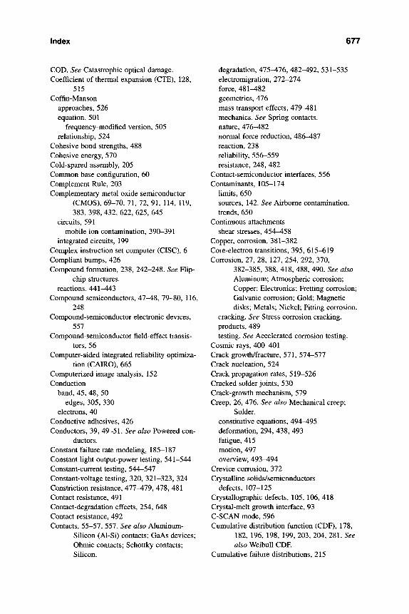
Index 677
COD. See Catastrophic optical damage. Coefficient of thermal expansion (CTE), 128,
515 Coffin-Manson
approaches, 526 equation, 501
frequency-modified version, 505 relationship, 524
Cohesive bond strengths, 488 Cohesive energy, 570 Cold-spared assembly, 205 Conmion base configuration, 60 Complement Rule, 203 Complementary metal oxide semiconductor
(CMOS), 69-70, 71, 72, 91, 114, 119, 383, 398, 432, 622, 625, 645
circuits, 591 mobile ion contamination, 390-391
integrated circuits, 199 Complex instruction set computer (CISC), 6 Compliant bumps, 426 Compound formation, 238, 242-248. See Flip-
chip structures, reactions, 441^43
Compound semiconductors, 4 7 ^ 8 , 79-80, 116, 248
Compound-semiconductor electronic devices, 557
Compound-semiconductor field-effect transis-tors, 56
Computer-aided integrated reliability optimiza-tion (CAIRO), 665
Computerized image analysis, 152 Conduction
band, 45, 48, 50 edges, 305, 330
electrons, 40 Conductive adhesives, 426 Conductors, 39, 49-51. See also Powered con-
ductors. Constant failure rate modeling, 185-187 Constant light output-power testing, 541-544 Constant-current testing, 544-547 Constant-voltage testing, 320, 321-323, 324 Constriction resistance, 477-479, 478, 481 Contact resistance, 491 Contact-degradation effects, 254, 648 Contact-resistance, 492 Contacts, 55-57, 557. See also Aluminum-
Silicon (Al-Si) contacts; GaAs devices; Ohmic contacts; Schottky contacts; Silicon.
degradation, 475^76, 482-492, 531-535 electromigration, 212-214 force, 481-482 geometries, 476 mass transport effects, 479^81 mechanics. See Spring contacts. nature, 476-482 normal force reduction, 486-487 reaction, 238 reliability, 556-559 resistance, 248, 482
Contact-semiconductor interfaces, 556 Contaminants, 105-174
limits, 650 sources, 142. See Airborne contamination. trends, 650
Continuous attachments shear stresses, 454-458
Copper, corrosion, 381-382 Core-electron transitions, 395, 615-619 Corrosion, 27, 28, 127, 254, 292, 370,
382-385, 388, 418, 488, 490. See also Aluminum; Atmospheric corrosion; Copper; Electronics; Fretting corrosion; Galvanic corrosion; Gold; Magnetic disks; Metals; Nickel; Pitting corrosion.
cracking. See Stress corrosion cracking. products, 489 testing. See Accelerated corrosion testing.
Cosmic rays, 400-401 Crack growth/fracture, 571, 574-577 Crack nucleation, 524 Crack propagation rates, 519-526 Cracked solder joints, 530 Crack-growth mechanism, 579 Creep, 26, 476. See also Mechanical creep;
Solder. constitutive equations, 494-495 deformation, 294, 438, 493 fatigue, 415 motion, 497 overview, 493-494
Crevice corrosion, 372 Crystalline solids/semiconductors
defects, 107-125 Crystallographic defects, 105, 106, 418 Crystal-melt growth interface, 93 C-SCAN mode, 596 Cumulative distribution function (CDF), 178,
182, 196, 198, 199, 203, 204, 281. See also WeibuU CDF
Cumulative failure distributions, 215
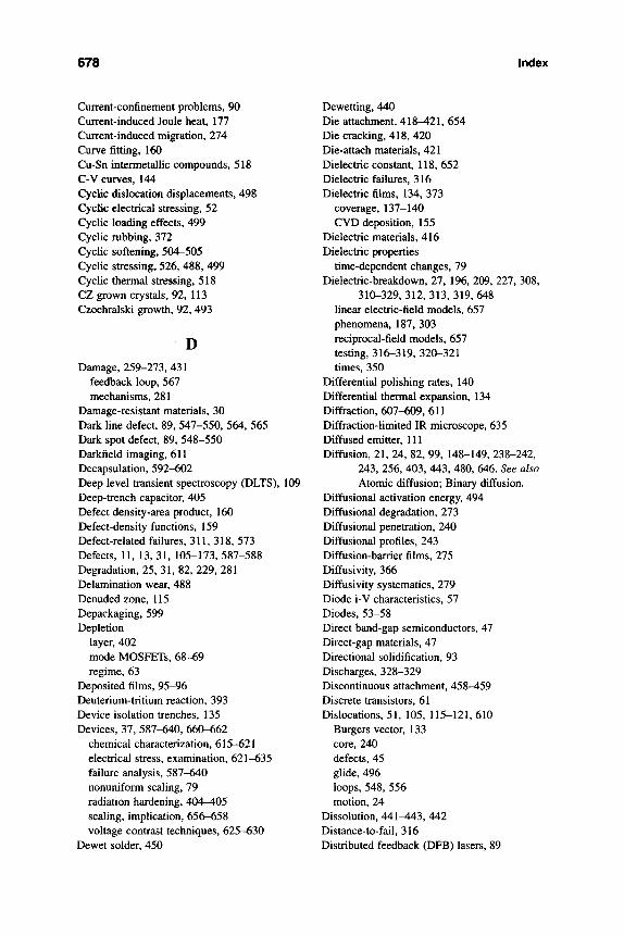
678 Index
Current-confinement problems, 90 Current-induced Joule heat, 177 Current-induced migration, 274 Curve fitting, 160 Cu-Sn intermetallic compounds, 518 C-V curves, 144 Cyclic dislocation displacements, 498 Cyclic electrical stressing, 52 Cyclic loading effects, 499 Cyclic rubbing, 372 Cyclic softening, 504-505 Cyclic stressing, 526, 488, 499 Cyclic thermal stressing, 518 CZ grown crystals, 92, 113 Czochralski growth, 92, 493
D Damage, 259-273, 431
feedback loop, 567 mechanisms, 281
Damage-resistant materials, 30 Dark line defect, 89, 547-550, 564, 565 Dark spot defect, 89, 548-550 Darkneld imaging, 611 Decapsulation, 592-602 Deep level transient spectroscopy (DLTS), 109 Deep-trench capacitor, 405 Defect density-area product, 160 Defect-density functions, 159 Defect-related failures, 311, 318, 573 Defects, 11, 13, 31, 105-173, 587-588 Degradation, 25, 31, 82, 229, 281 Delamination wear, 488 Denuded zone, 115 Depackaging, 599 Depletion
layer, 402 mode MOSFETs, 68-69 regime, 63
Deposited films, 95-96 Deuterium-tritium reaction, 393 Device isolation trenches, 135 Devices, 37, 587-640, 660-662
chemical characterization, 615-621 electrical stress, examination, 621-635 failure analysis, 587-640 nonuniform scaling, 79 radiation hardening, 404-405 scaling, impUcation, 656-658 voltage contrast techniques, 625-630
Dewet solder, 450
Dewetting, 440 Die attachment, 418-421, 654 Die cracking, 418, 420 Die-attach materials, 421 Dielectric constant, 118, 652 Dielectric failures, 316 Dielectric films, 134, 373
coverage, 137-140 CVD deposition, 155
Dielectric materials, 416 Dielectric properties
time-dependent changes, 79 Dielectric-breakdown, 27, 196, 209, 227, 308,
310-329, 312, 313, 319, 648 linear electric-field models, 657 phenomena, 187, 303 reciprocal-field models, 657 testing, 316-319, 320-321 times, 350
Differential polishing rates, 140 Differential thermal expansion, 134 Diffraction, 607-609, 611 Diffraction-limited IR microscope, 635 Diffused emitter, 111 Diffusion, 21, 24, 82, 99, 148-149, 238-242,
243, 256, 403, 443, 480, 646, See also Atomic diffusion; Binary diffusion.
Diffusional activation energy, 494 Diffusional degradation, 273 Diffusional penetration, 240 Diffusional profiles, 243 Diffusion-barrier films, 275 Diffusivity, 366 Diffusivity systematics, 279 Diode i-V characteristics, 57 Diodes, 53-58 Direct band-gap semiconductors, 47 Direct-gap materials, 47 Directional solidification, 93 Discharges, 328-329 Discontinuous attachment, 458-459 Discrete transistors, 61 Dislocations, 51, 105, 115-121, 610
Burgers vector, 133 core, 240 defects, 45 ghde, 496 loops, 548, 556 motion, 24
Dissolution, 441^W3, 442 Distance-to-fail, 316 Distributed feedback (DFB) lasers, 89

Index 679
Dopant diffusion profiles, 112 Dopant-bearing contaminants, 650 Doped n-channel, 74 Doped p-layers, 74 Doping concentration, 110 Dormancy, 16 Dose rate, 392 Double diffused drain (DDD), 338 Double-heterojunction lasers, 88 Drag, 147 Drain avalanche hot carrier (DAHC), 331 Drain depletion region, 68 Drain regions, 66 Drain-source current, 72 Driving forces, 20-24 Dual in-line package (DIP), 411, 428, 448, 599 Dynamic random access memory (DRAM), 10,
74, 75, 77, 106, 123-125, 135, 138, 146, 401, 403, 405, 630, 642, 647, 650
Dynamic-loading effects, 526
E Early-life reliability prediction, 226 Edge dislocation, 115 Edge-emitting diodes (EED), 86-87 EEPROM, 75, 77, 119 Elastic strain/plastic strain, 510-511 Electric field-induced metal migration, 254 Electrical overstress (EOS), 28, 29, 228,
339-352, 556 introduction, 339-341
Electrical stress failures, 27, 28 Electrode area-dependent breakdown effects,
325 Electrode sinking, 557 Electrode-solder interface, 557 Electroluminescence (EL), 548 Electrolytic corrosion, 441 Electromagnetic limits, 660 Electromagnetic waves, 2 Electromigration, 50, 51, 82, 136, 187, 254,
259-273, 273-284, 281-283, 288-289, 376, 435, 479, 480, 588, 656. See Con-tacts; Grain boundaries; Interconnects; Vias.
Electromigration-induced damage, 284 Electromigration-induced spiking, 557 Electron backscatter diffraction (EBSD), 280,
607 Electron beam testing (EBT) methods, 625,
626
Electron beam-induced current (EBIC), 610, 613, 624, 626-630
Electron energy loss spectroscopy (EELS), 611 Electron microscopy, 604-610, 613 Electron saturation velocity, 81, 661 Electron-atom interactions, 303 Electron-beam source, 137 Electron-defect centers, 580 Electron-hole pairs, 396, 397, 404, 560, 609 Electron-hole recombination, 48, 53, 116, 580 Electronic charge-induced damage, 303-357
exercises, 352-355 introduction, 303-304
Electronic devices, 1-36, 212 fabrication process, 37-104 radiation damage, 391^05
Electronic equipment, 218 dynamic loading effects, 526-531
introduction, 526-527 unreliability, 14 vibration, 527-531
Electronic packaging, 488, 495 Electron-metal interactions, 303 Electro-optical applications, 47 Electro-optical devices, 84-91, 221, 340, 393,
398, 539-540, 554, 569, 582-585 degradation/failure, 539-586
Electro-optical effects, 49, 560 Electro-optical materials, 539-540, 582-585
degradation/failure, 539-586 Electro-optical systems, 540 Electrostatic adhesion, 147, 151 Electrostatic damage, 339-341 Electrostatic discharge (ESD), 28, 29, 89-90,
228, 303, 308, 339-352, 591, 600, 622, 631
Electrothermomigration-induced mass trans-port, 347
Electrotransport, 267 Emission microscopy, 621-625, 623. See also
Light emission microscopy. Emitter-push effect, 112 Encapsulants, 431 Encapsulated ICs, 596 End-of-life (EOL), 544 Energy barriers, 20, 21. See also Lattice energy
barriers. Energy gap, 45, 50 Energy-dispersive X-ray analysis (EDX), 607,
611, 615-617 Enthalpies, 19, 20 Environmental factors, 29
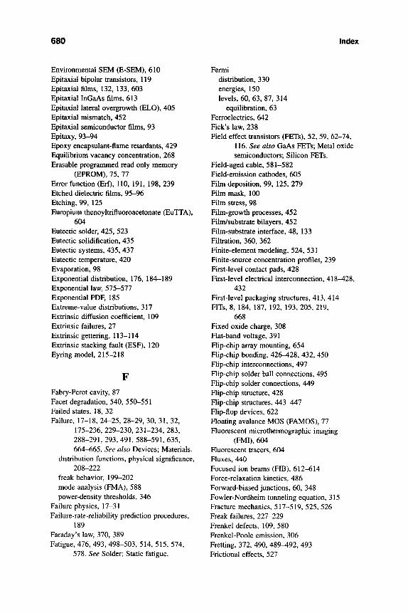
680 Index
Environmental SEM (E-SEM), 610 Epitaxial bipolar transistors, 119 Epitaxial films, 132, 133, 603 Epitaxial InGaAs films, 613 Epitaxial lateral overgrowth (ELO), 405 Epitaxial mismatch, 452 Epitaxial semiconductor films, 93 Epitaxy, 93-94 Epoxy encapsulant-flame retardants, 429 Equilibrium vacancy concentration, 268 Erasable programmed read only memory
(EPROM), 75, 77 Error function (Erf), 110, 191, 198, 239 Etched dielectric films, 95-96 Etching, 99, 125 Europium thenoyltrifluoroacetonate (EuTTA),
604 Eutectic solder, 425, 523 Eutectic solidification, 435 Eutectic systems, 435, 437 Eutectic temperature, 420 Evaporation, 98 Exponential distribution, 176, 184-189 Exponential law, 575-577 Exponential PDF, 185 Extreme-value distributions, 317 Extrinsic diffusion coefficient, 109 Extrinsic failures, 27 Extrinsic gettering, 113-114 Extrinsic stacking fault (ESP), 120 Eyring model, 215-218
Fabry-Perot cavity, 87 Facet degradation, 540, 550-551 Failed states, 18, 32 Failure, 17-18, 24-25, 28-29, 30, 31, 32,
175-236, 229-230, 231-234, 283, 288-291, 293, 491, 588-591, 635, 664-665. See also Devices; Materials,
distribution functions, physical significance, 208-222
freak behavior, 199-202 mode analysis (FMA), 588 power-density thresholds, 346
Failure physics, 17-31 Failure-rate-reliability prediction procedures,
189 Faraday's law, 370, 389 Fatigue, 476, 493, 498-503, 514, 515, 574,
578. See Solder; Static fatigue.
Fermi distribution, 330 energies, 150 levels, 60, 63, 87, 314
equilibration, 63 Ferroelectrics, 642 Pick's law, 238 Field effect transistors (FETs), 52, 59, 62-74,
116. See also GaAs FETs; Metal oxide semiconductors; Silicon FETs.
Field-aged cable, 581-582 Field-emission cathodes, 605 Film deposition, 99, 125, 279 Film mask, 100 Film stress, 98 Film-growth processes, 452 Film/substrate bilayers, 452 Film-substrate interface, 48, 133 Filtration, 360, 362 Finite-element modehng, 524, 531 Finite-source concentration profiles, 239 First-level contact pads, 428 First-level electrical interconnection, 418^28,
432 First-level packaging structures, 413, 414 FITS, 8, 184, 187, 192, 193, 205, 219,
668 Fixed oxide charge, 308 Flat-band voltage, 391 Flip-chip array mounting, 654 Flip-chip bonding, 426-428, 432, 450 Hip-chip interconnections, 497 Flip-chip solder ball connections, 495 Flip-chip solder connections, 449 Hip-chip structure, 428 Hip-chip structures, 443^447 Hip-flop devices, 622 Hoating avalance MOS (FAMOS), 77 Fluorescent microthermographic imaging
(FMI), 604 Huorescent tracers, 604 Fluxes, 440 Focused ion beams (FIB), 612-614 Force-relaxation kinetics, 486 Forward-biased junctions, 60, 348 Fowler-Nordheim tunneling equation, 315 Fracture mechanics, 517-519, 525, 526 Freak failures, 227-229 Frenkel defects, 109, 580 Frenkel-Poole emission, 306 Fretting, 372, 490, 489^92, 493 Frictional effects, 527
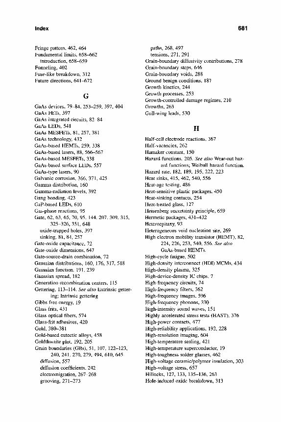
Index 681
Fringe pattern, 462, 464 Fundamental limits, 658-662
introduction, 658-659 Funneling, 402 Fuse-like breakdown, 312 Future directions, 641-672
GaAs devices, 79-84, 253-259, 397, 404 GaAs FETs, 397 GaAs integrated circuits, 82-84 GaAs LEDs, 541 GaAs MESFETs, 81, 257, 381 GaAs technology, 432 GaAs-based HEMTs, 259, 338 GaAs-based lasers, 88, 566-567 GaAs-based MESFETs, 338 GaAs-based surface LEDs, 557 GaAs-type lasers, 90 Galvanic corrosion, 366, 371, 425 Gamma distribution, 160 Gamma-radiation levels, 392 Gang bonding, 423 GaP-based LEDs, 610 Gas-phase reactions, 95 Gate, 62, 63, 65, 70, 95, 144, 207, 309, 315,
325-326, 351, 648 oxide-trapped holes, 397 sinking, 81, 84, 257
Gate-oxide capacitance, 72 Gate-oxide dimensions, 647 Gate-source-drain combination, 72 Gaussian distributions, 160, 176, 317, 518 Gaussian function, 191, 239 Gaussian spread, 182 Generation-recombination centers, 115 Gettering, 113-114. See also Extrinsic getter-
ing; Intrinsic gettering Gibbs free energy, 19 Glass frits, 431 Glass optical fibers, 574 Glass-frit adhesives, 420 Gold, 380-381 Gold-based eutectic alloys, 458 Goldthwaite plot, 192, 205 Grain boundaries (GBs), 51, 107, 122-123,
240, 241, 270, 279, 494, 610, 645 diffusion, 557 diffusion coefficients, 242 electromigration, 267-268 grooving, 271-273
paths, 268, 497 tensions, 271, 291
Grain-boundary diffusivity contributions, 278 Grain-boundary steps, 646 Grain-boundary voids, 288 Ground benign conditions, 187 Growth kinetics, 244 Growth processes, 253 Growth-controlled damage regimes, 210 Growths, 263 Gull-wing leads, 530
H Half-cell electrode reactions, 367 Half-vacancies, 262 Hamaker constant, 150 Hazard functions, 205. See also Wear-out haz-
ard functions; WeibuU hazard function. Hazard rate, 182, 189, 195, 222, 223 Heat sinks, 415, 462, 540, 556 Heat-age testing, 486 Heat-sensitive plastic packages, 450 Heat-sinking contacts, 254 Heat-treated glass, 127 Heisenberg uncertainty principle, 659 Hermetic packages, 431^32 Heteroepitaxy, 93 Heterogeneous void nucleation site, 269 High electron mobility transistor (HEMT), 82,
224, 226, 253, 540, 556. See also GaAs-based HEMTs.
High-cycle fatigue, 502 High-density interconnect (HDI) MCMs, 434 High-density plasma, 325 High-device-density IC chips, 7 High-frequency circuits, 74 High-frequency filters, 362 High-frequency images, 596 High-frequency phonons, 330 High-intensity sound waves, 151 Highly accelerated stress tests (HAST), 376 High-power contacts, 477 High-reliability appHcations, 192, 228 High-resolution imaging, 604 High-temperature sealing, 421 High-temperature superconductor, 19 High-toughness solder glasses, 462 High-voltage ceramic/polymer insulation, 303 High-voltage stress, 657 Hillocks, 127, 133, 135-136, 263 Hole-induced oxide breakdown, 313
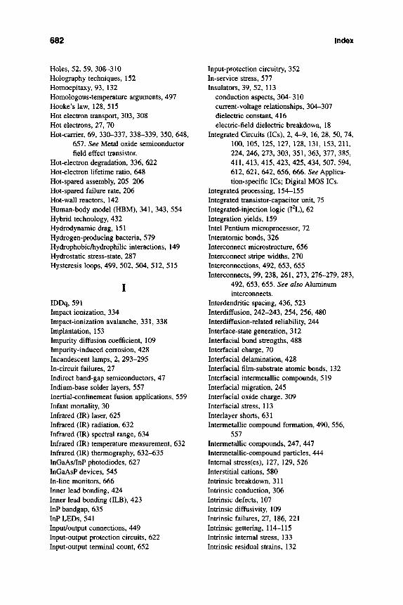
682 Index
Holes, 52, 59, 308-310 Holography techniques, 152 Homoepitaxy, 93, 132 Homologous-temperature arguments, 497 Hooke'slaw, 128,515 Hot electron transport, 303, 308 Hot electrons, 27, 70 Hot-carrier, 69, 330-337, 338-339, 350, 648,
657, See Metal oxide semiconductor field effect transistor.
Hot-electron degradation, 336, 622 Hot-electron lifetime ratio, 648 Hot-spared assembly, 205-206 Hot-spared failure rate, 206 Hot-wall reactors, 142 Human-body model (HBM), 341, 343, 554 Hybrid technology, 432 Hydrodynamic drag, 151 Hydrogen-producing bacteria, 579 Hydrophobic/hydrophilic interactions, 149 Hydrostatic stress-state, 287 Hysteresis loops, 499, 502, 504, 512, 515
I IDDq, 591 Impact ionization, 334 Impact-ionization avalanche, 331, 338 Implantation, 153 Impurity diffusion coefficient, 109 Impurity-induced corrosion, 428 Incandescent lamps, 2, 293-295 In-circuit failures, 27 Indirect band-gap semiconductors, 47 Indium-base solder layers, 557 Inertial-confinement fusion applications, 559 Infant mortality, 30 Infrared (IR) laser, 625 Infrared (IR) radiation, 632 Infrared (IR) spectral range, 634 Infrared (IR) temperature measurement, 632 Infrared (IR) thermography, 632-635 InGaAs/InP photodiodes, 627 InGaAsP devices, 545 In-line monitors, 666 Inner lead bonding, 424 Inner lead bonding (ILB), 423 InP bandgap, 635 InPLEDs, 541 Input/output connections, 449 Input-output protection circuits, 622 Input-output terminal count, 652
Input-protection circuitry, 352 In-service stress, 577 Insulators, 39,52, 113
conduction aspects, 304-310 current-voltage relationships, 304-307 dielectric constant, 416 electric-field dielectric breakdown, 18
Integrated Circuits (ICs), 2, 4-9, 16, 28, 50, 74, 100, 105, 125, 127, 128, 131, 153, 211, 224, 246, 273, 303, 351, 363, 377, 385, 411, 413, 415, 423, 425, 434, 507, 594, 612, 621, 642, 656, 666. See Applica-tion-specific ICs; Digital MOS ICs.
Integrated processing, 154-155 Integrated transistor-capacitor unit, 75 Integrated-injection logic (I^L), 62 Integration yields, 159 Intel Pentium microprocessor, 72 Interatomic bonds, 326 Interconnect microstructure, 656 Interconnect stripe widths, 270 Interconnections, 492, 653, 655 Interconnects, 99, 238, 261, 273, 276-279, 283,
492, 653, 655. See also Aluminum interconnects.
Interdendritic spacing, 436, 523 Interdiffusion, 242-243, 254, 256, 480 Interdiffusion-related reliability, 244 Interface-state generation, 312 Interfacial bond strengths, 488 Interfacial charge, 70 Interfacial delamination, 428 Interfacial film-substrate atomic bonds, 132 Interfacial intermetallic compounds, 519 Interfacial migration, 245 Interfacial oxide charge, 309 Interfacial stress, 113 Interlayer shorts, 631 Intermetallic compound formation, 490, 556,
557 Intermetallic compounds, 247, 447 Intermetallic-compound particles, 444 Internal stress(es), 127, 129, 526 Interstitial cations, 580 Intrinsic breakdown, 311 Intrinsic conduction, 306 Intrinsic defects, 107 Intrinsic diffusivity, 109 Intrinsic failures, 27, 186, 221 Intrinsic gettering, 114-115 Intrinsic internal stress, 133 Intrinsic residual strains, 132
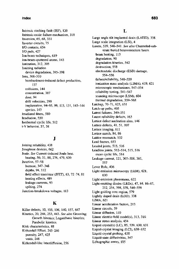
Index 683
Intrinsic stacking fault (ISF), 120 Intrinsic-oxide failure-mechanism, 318 Inversion, 65, 68, 331 Inverter circuits, 75 I/O contacts, 654 I/O pads, 427 Ion-beam techniques, 619 lon-beam-sputtered atoms, 143 Ionization, 312, 395 Ionizing radiation
device degradation, 395-398 Ions, 308-310
bombardment-induced defect production, 137
collisions, 144 concentration, 387 dose, 94 drift velocities, 390 implantation, 94-95, 99, 113, 131, 143-144 species, 143
Irradiated fibers, 580 Irradiation, 550 Isothermal cyclic life, 512 i-V behavior, 57, 58
Joining reliability, 438 Josephson devices, 662 Joule. See Current-induced Joule heat.
heating, 50, 51, 88, 276, 479, 630 Junction, 57-58
burnout, 347-348 depths, 94, 112 field effect transistor (JFET), 63, 72-74, 81 heating effects, 489 leakage currents, 93 spiking, 274
Junction-breakdown voltages, 113
K Killer defects, 10, 105, 106, 140, 157, 647 Kinetics, 20, 244, 253, 443, See also Grooving;
Growth kinetics; Logarithmic kinetics; Parabolic kinetics.
Kink characteristics, 88 Kirkendall Effect, 245-246
porosity, 247, 425 voids, 248
Kirkendall-like interdiffusion, 256
Large angle tilt implanted drain (LATID), 338 Large scale integration (LSI), 4 Lasers, 539, 540-541. See also Channeled-sub-
strate buried heterostructure lasers beam heating, 113 degradation, 90 degradation kinetics, 542 destruction, 558 electrostatic discharge (ESD) damage,
554-556 failure/reliability, 540-559 ionization mass analysis (LIMA), 619, 621 microscopic mechanisms, 547-554 reliability testing, 541-547 scanning microscope (LSM), 604 thermal degradation, 559-568
Latchup, 70-71, 625, 631 Latch-up paths, 405 Latent failures, 349-351 Latent reliability defects, 163 Lattice defect nucleation sites, 146 Lattice defects, 41, 51, 107 Lattice imaging, 611 Lattice match, 84, 86 Lattice mismatch, 132 Lead frames, 653 Leaded joints, 515,516 Leadless joints, 512-514, 515, 516
mean cyclic life, 514 Leakage current, 121, 307-308, 381,
557 Lever Rule, 436 Light emission microscopy (LEM), 621,
630 Light-emission phenomena, 622 Light-emitting diodes (LEDs), 47, 84, 86-87,
212, 254, 398, 539, 540-559 Light-guiding core region, 579 Lightly doped drain (LDD), 338 LIMA, 621 Linear acceleration factors, 213 Linear circuits, 59 Linear diffusion, 110 Linear electric-field model(s), 313, 316 Linear stress analysis, 454 Liquid crystal(s) (LC), 85, 539, 630, 631 Liquid-crystal imaging (LCI), 630-632 Liquid-crystal probing, 630 Liquid-state diffusivities, 347 Lithographic errors, 105
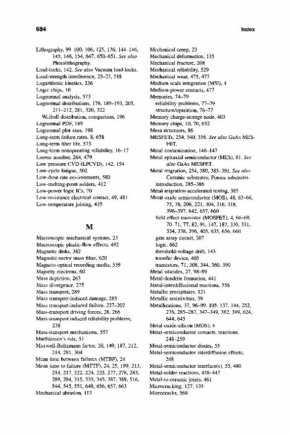
684 Index
Lithography, 99-100, 106, 125, 136, 144-146, 145, 146, 154, 647, 650-651. See also Photolithography.
Load-locks, 142. See also Vacuum load-locks. Load-strength interference, 25-27, 518 Logarithmic kinetics, 336 Logic chips, 10 Lognormal analysis, 573 Lognormal distributions, 176, 189-193, 205,
211-212,281,320,322 WubuU distribution, comparison, 196
Lognormal PDF, 189 Lognormal plot axes, 198 Long-term failure rates, 8, 658 Long-term fiber life, 573 Long-term nonoperating reliability, 16-17 Lorenz number, 264, 479 Low pressure CVD (LPCVD), 142, 154 Low-cycle fatigue, 502 Low-dose rate environments, 580 Low-melting-point solders, 412 Low-power logic ICs, 70 Low-resistance electrical contact, 49, 481 Low-temperature joining, 435
M Macroscopic mechanical systems, 23 Macroscopic plastic-flow effects, 492 Magnetic disks, 382 Magnetic-sector mass filter, 620 Magneto-optical recording media, 539 Majority electrons, 60 Mass depletion, 263 Mass divergence, 275 Mass transport, 289 Mass transport-induced damage, 285 Mass transport-induced failure, 237-302 Mass-transport driving forces, 28, 266 Mass-transport induced reliability problems,
238 Mass-transport mechanisms, 557 Matthiessen's rule, 51 Maxwell-Boltzmann factor, 20, 149, 187, 212,
214, 281, 304 Mean time between failures (MTBF), 24 Mean time to failure (MTTF), 24, 25, 199, 213,
214, 217, 222, 224, 225, 277, 278, 283, 289, 294, 315, 335, 345, 387, 389, 516, 544, 545, 551, 648, 656, 657, 663
Mechanical abrasion, 113
Mechanical creep, 23 Mechanical deformation, 135 Mechanical fracture, 208 Mechanical reUability, 529 Mechanical wear, 475, 477 Medium scale integration (MSI), 4 Medium-power contacts, 477 Memories, 74-79
reliability problems, 77-79 structure/operation, 76-77
Memory charge-storage node, 403 Memory chips, 10, 70, 652 Mesa structures, 86 MESFETs, 254, 540, 556. See also GaAs MES-
FET. Metal contamination, 146-147 Metal epitaxial semiconductor (MES), 81. See
also GaAs MESFET. Metal migration, 254, 380, 385-391. See also
Ceramic substrates; Porous substrates, introduction, 385-386
Metal migration-accelerated testing, 385 Metal oxide semiconductor (MOS), 48, 63-66,
75,76,206,221,304,316,318, 396-397, 642, 657, 660
field effect transistor (MOSFET), 4, 66-69, 70-71, 77, 82, 91, 147, 187, 330, 331, 334, 338, 396, 405, 635, 656, 660
gate array circuit, 207 logic, 662 threshold-voltage drift, 143 transfer device, 405 transistors, 71, 308, 344, 360, 390
Metal silicides, 27, 98-99 Metal-dendrite formation, 441 Metal-interdiffusional reactions, 556 Metallic precipitates, 121 Metallic resistivities, 39 Metallizations, 37, 96-99, 105, 137, 144, 252,
276, 285-287, 347-349, 382, 399, 624, 644,645
Metal-oxide-silicon (MOS), 4 Metal-semiconductor contacts, reactions,
248-259 Metal-semiconductor diodes, 55 Metal-semiconductor interdiffusion effects,
248 Metal-semiconductor interface(s), 55, 480 Metal-solder reactions, 438^47 Metal-to-ceramic joints, 461 Microcracking, 127, 135 Microcracks, 569
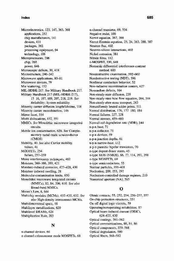
Index 685
Microelectronics, 123, 147, 363, 368 applications, 252 chip manufacturers, 141 devices, 411 packages, 382 processing equipment, 94 technology, 106
Microprocessors, 206 chip, 260 power, 646
Microscopic defects, 30, 418 Microstructure, 240-242 Microwave applications, 80-81 Microwave devices, 79 Mie scattering, 152 MIL-HDBK-217. See Military Handbook 217. Military Handbook 217 (MIL-HDBK-217),
15-16, 187, 189, 207, 218, 219. See Reliability; System reliability.
Minority carrier diffusion length/lifetime, 118 Minority carrier recombination, 146 Mirror facet, 554 Misfit dislocations, 132, 551 MMICs. See Monolithic microwave integrated
circuits. Mobile ion contamination, 620. See Comple-
mentary metal oxide semiconductor (CMOS)
Mobility, 40. See also Carrier mobility. values, 41
MODFETs, 254 failure, 257-259
Moire interferometry techniques, 462 Moisture, 360-366, 389, 421 Moisture-induced corrosion, 427^28, 430 Moisture-induced swelling, 28 Molecular-contamination limits, 650 Monolithic microwave integrated circuits
(MMICs), 82, 84, 206, 610. See also Broad-band MMICs.
Moore's Law, 6, 644 Multichip modules (MCMs), 432-435, 652. See
also High-density interconnect MCMs. Multidimensional space, 18 Multilayer metallizations, 620 Multilevel DRAMs, 624 Multiplication Rule, 203
N n-channel devices, 66 n-channel enhancement mode MOSFETs, 68
n-channel transistor, 69, 334 Negative resist, 100 Nemst equation, 367, 368 Nemst-Einstein equation, 23, 24, 263, 288, 387 Neutron flux, 402 Neutron-silicon interactions, 402 Nickel corrosion, 381 Nitride films, 112 n-MOSFET, 330, 648 Nomarski differential interference-contrast
method, 603 Nondestructive examination, 592-602 Nondestructive testing (NDT), 596 NonUnear conduction behavior, 52 Non-radiative recombination centers, 627 Nonrandom defects, 164 Non-steady-state diffusion, 239 Non-steady-state heat flow equation, 264, 344 Non-steady-state mass transport, 263 Nonuniformly heated solder joints, 511 Normal distribution, 176, 177-180, 184 Normal failures, 227, 228 Normal stresses, 459-460 Normalized degradation rate (NDR), 544 n-p-n base, 71 n-p-n collector, 71 n-p-n devices, 59 n-p-n junction depths, 61 n-p-n narrow-base, 112 n-p-n parasitic bipolar transistors, 70 n-type dopant donor states, 45 n-type MOS (NMOS), 66, 77, 114, 391, 398 n-type MOSFETs, 69 n-type semiconductors, 55 Nuclear particles, 399^01 Nucleation, 209, 253, 292 Nucleation-controUed damage regimes, 210 Numerical aperture (NA), 595
o Ohmic contacts, 55, 252, 254, 256-257, 557 On-chip protection structures, 351 On-off digital logic circuits, 59 Operating/nonoperating reliabilities, 17 Optical beam-induced current (OBIC),
624-625, 630 Optical coatings, 561-562 Optical communications, 80, 84, 86 Optical components, 559-568 Optical degradation, 580 Optical fibers, 568-582
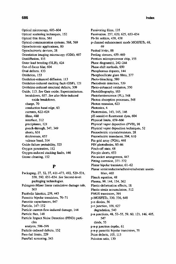
686 Index
Optical microscopy, 603-604 Optical scattering techniques, 152 Optical thin films, 561 Optical-communication systems, 568, 569 Optoelectronic applications, 80 Optoelectronic devices, 28 Orientation imaging microscopy (OIM), 607 Outdiffusion, 115 Outer lead bonding (OLB), 424 Out-of-focus blur, 604 Oval defects, 133 Oxidation, 153 Oxidation-enhanced diffusion, 113 Oxidation-induced stacking fault (OSF), 121 Oxidation-induced structural defects, 309 Oxide, 113. See Gate oxide; Superconductors.
breakdown, 657. See also Hole-induced oxide breakdown.
charge, 70 conduction band edge, 63 currents, 622-624 films, 488 interface, 312 precipitates, 121 punch-through, 347, 349 shorts, 631 thicknesses, 657 valence band, 314
Oxide-failure probability, 325 Oxygen penetration, 112 Oxygen-induced stacking faults, 146 Ozone cleaning, 152
Packaging, 27, 32, 37, 411-473, 492, 529-531, 558, 592, 651-654. See Second-level packaging technologies.
Palmgren-Miner linear cumulative damage rule, 503
Parabolic kinetics, 259, 443 Parasitic bipolar transistors, 70-71 Parasitic capacitances, 647 Particle, 147-152 Particle current-flow-induced damage, 144 Particle flux, 148 Particle Impact Noise Detection (PIND) parti-
cles analysis, 598-599
Particle-induced defects, 152 Pass-fail limits, 229 Pass/fail screening, 543
Passivating films, 135 Passivation, 257, 620, 625, 653-654 Pb-Sn solders, 438, 458 p-channel enhancement mode MOSFETs, 68,
69 Peaked kinks, 88 Peeling stresses, 459-460 Pentium microprocessor chip, 155 Phase diagram(s), 242-244 Phase-shift methods, 650 Phosphorous dopants, 144 Phosphosilicate glass films, 377 Photo-bleaching, 580 Photodiode detectors, 539 Photo-enhanced oxidation, 550 Photolithography, 163 Photoluminescence (PL), 548 Photon absorption processes, 548 Photon emission, 623 Photonics, 4 Photoresists, 143, 145, 146 pH-sensitive fluorescent dyes, 604 Physical Umits, 659-660 Physical vapor deposition (PVD), 98 Physical vapor deposition techniques, 52 Piezoelectric crystals/resistors, 28 Piezoelectric transducer, 594, 610 Pin grid array (PGA), 448 PIN photodiodes, 85-86 Pinch-off state, 68 Pin-pin shorts, 653 Pin-socket arrangement, 447 Pitting corrosion, 371-372 Planar bipolar transistor, 61-62 Planar semiconductor/adhesive/substrate assem-
blies, 460 Planck equation, 48 Plasma, 99, 144, 154, 562 Plastic-deformation effects, 18 Plastic-strain accumulation, 512 PMOS transistors, 391 p-MOSFETs, 330, 336, 648 p-n diodes, 56 p-n junction, 109, 627
degradation, 540 p-n junctions, 48, 53-55, 59, 60, 121, 146, 405,
547 diode, 55
p-n-p junction depths, 61 p-n-p parasitic bipolar transistors, 70 Point defects, 105, 113 Poission ratio, 130
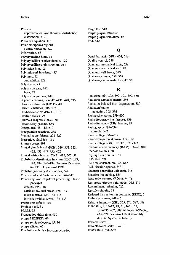
index 687
Poisson approximation. See Binomial distribution. distribution, 319
Poisson's equation, 116 Polar amorphous regions
electro-oxidation, 329 Polarization, 631 Polycrystalline films, 95 Polycrystalline semiconductors, 122 Poly crystalline-grain structure, 561 Polyimide film, 424 Polyimide-Al interface, 435 Polymers, 52
degradation, 329 Polysilicon, 95 Polysilicon gate, 622
layer, 77 Polysilicon patterns, 144 Popcorn cracking, 364, 429^31, 449, 596 Porous oxidized Si (FIPOS), 405 Porous substrates, 386-387 Position-sensitive detector, 137 Positive resists, 99 Pourbaix diagrams, 367-370 Power-delay product, 655 Precipitates, 45, 115, 610 Precipitation reactions, 238 Prediction confidence, 222-229 Pressurized fluid jets, 151 Primary creep, 493 Printed circuit board (PCB), 340, 352, 382,
412,431,447-450,462 Printed wiring boards (PWB), 412, 507, 511 Probability, distribution function (PDF), 179,
182, 184, 196-199. See also Exponen-tial PDF; Lognormal PDF.
Probability-density distributions, 664 Process-induced contamination, 142-147 Processing. See Chip-level processing; Plastic
packages defects, 125-140 extrinsic residual stress, 128-133 internal stress, 128, 133-137 intrinsic residual stress, 131-133
Processing defects, 107 Product yield, 31 PROM, 75 Propagation delay time, 659 p-type MOSFETs, 69 p-type semiconductors, 45, 76 p-type silicon, 66 Punch-through. See Junction behavior.
Purge test, 543 Purple plague, 246-248 Purple plague formation, 423 PZT, 642
Quad flat-pack (QFP), 464, 516 Quahty control, 588 Quantum-mechanical limit, 659 Quantum-mechanical well, 82 Quantum-well lasers, 540 Quaternary lasers, 550, 567 Quaternary semiconductors, 47, 79
R Radiation, 264, 308, 392-393, 399, 560 Radiation-damaged matrix, 393 Radiation-induced fiber degradation, 580 Radiation/matter
interaction, 393-395 Radioactive atoms, 399^00 Radio-frequency interference, 339 Radio-frequency (RF) plasmas, 99 Radiography, 592-594
example, 592 Ramp voltage, 316-319 Ramp-voltage breakdown, 317-319 Ramp-voltage tests, 317, 320, 321-323 Random access memory (RAM), 74-76, 400 Random failures, 30 Rayleigh distribution, 195 RBS, 620-621 RC time constant, 50, 646, 647 RCL circuit response, 343 Reaction-controlled oxidation, 245 Reactive ion etching, 155 Read only memory (ROM), 74-76 Reciprocal electric-field model, 313-316 Recombinant radiation, 622 Rectifier circuits, 58 Reduced instruction set computer (RISC), 6 Reflow processes, 449^51 Relative humidity (RH), 363, 375, 387, 389 Reliability, 3, 13-17, 29, 31, 163, 165,
175-236, 432, 588, 641-642, 662-668, 669-671. See also Latent reliability defects; System Reliability.
Reliable states, 18 Reliable/failed states, 17-18 Rent's Rule, 651-652
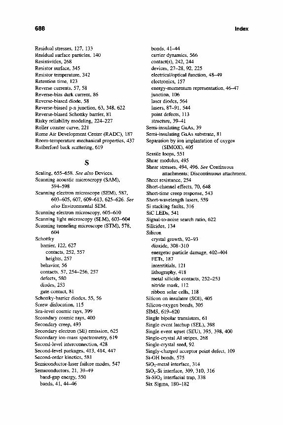
688 Index
Residual stresses, 127, 133 Residual surface particles, 140 Resistivities, 268 Resistor surface, 345 Resistor temperature, 342 Retention time, 123 Reverse currents, 57, 58 Reverse-bias dark current, 86 Reverse-biased diode, 58 Reverse-biased p-n junction, 63, 348, 622 Reverse-biased Schottky barrier, 81 Risky reliability modeling, 224-227 Roller coaster curve, 221 Rome Air Development Center (RADC), 187 Room-temperature mechanical properties, 437 Rutherford back scattering, 619
Scaling, 655-658. See also Devices. Scanning acoustic microscropy (SAM),
594-598 Scanning electron microscope (SEM), 587,
603-605, 607, 609-613, 625-626. See also Environmental SEM.
Scanning electron microscopy, 605-610 Scanning light microscopy (SLM), 603-604 Scanning tunneling microscope (STM), 578,
604 Schottky
barrier, 122, 627 contacts, 252, 557 heights, 257
behavior, 56 contacts, 57, 254-256, 257 defects, 580 diodes, 253 gate contact, 81
Schottky-barrier diodes, 55, 56 Screw dislocation, 115 Sea-level cosmic rays, 399 Secondary cosmic rays, 400 Secondary creep, 493 Secondary electron (SE) emission, 625 Secondary ion-mass spectrometry, 619 Second-level interconnection, 428 Second-level packages, 413, 414, 447 Second-order kinetics, 581 Semiconductor-laser failure modes, 547 Semiconductors, 21, 39-49
band-gap energy, 550 bands, 41, 44-46
bonds, 41-44 carrier dynamics, 566 contact(s), 242, 244 devices, 27-28, 92, 225 electrical/optical function, 48-49 electronics, 157 energy-momentum representation, 46-47 junction, 106 laser diodes, 564 lasers, 87-91, 544 point defects, 113 structure, 3 9 ^ 1
Semi-insulating GaAs, 39 Semi-insulating GaAs substrate, 81 Separation by ion implantation of oxygen
(SIMOX), 405 Sessile loops, 551 Shear modulus, 495 Shear stresses, 494, 496. See Continuous
attachments; Discontinuous attachment. Sheet resistance, 254 Short-channel effects, 70, 648 Short-time creep response, 543 Short-wavelength lasers, 559 Si stacking faults, 316 SiC LEDs, 541 Signal-to-noise search ratio, 622 Silicides, 134 Silicon
crystal growth, 92-93 dioxide, 308-310 energetic particle damage, 402-404 FETs, 187 interstitials, 121 hthography, 418 metal silicide contacts, 252-253 nitride mask, 112 ribbon solar cells, 118
Silicon on insulator (SOI), 405 Silicon-oxygen bonds, 305 SIMS, 619-620 Single bipolar transistors, 61 Single event latchup (SEL), 398 Single event upset (SEU), 395, 398, 400 Single-crystal Al stripes, 268 Single-crystal seed, 92 Singly-charged acceptor point defect, 109 Si-OH bonds, 575 Si02-metal interface, 314 Si02-Si interface, 309, 310, 316 Si-Si02 interfacial trap, 338 Six Sigma, 180-182
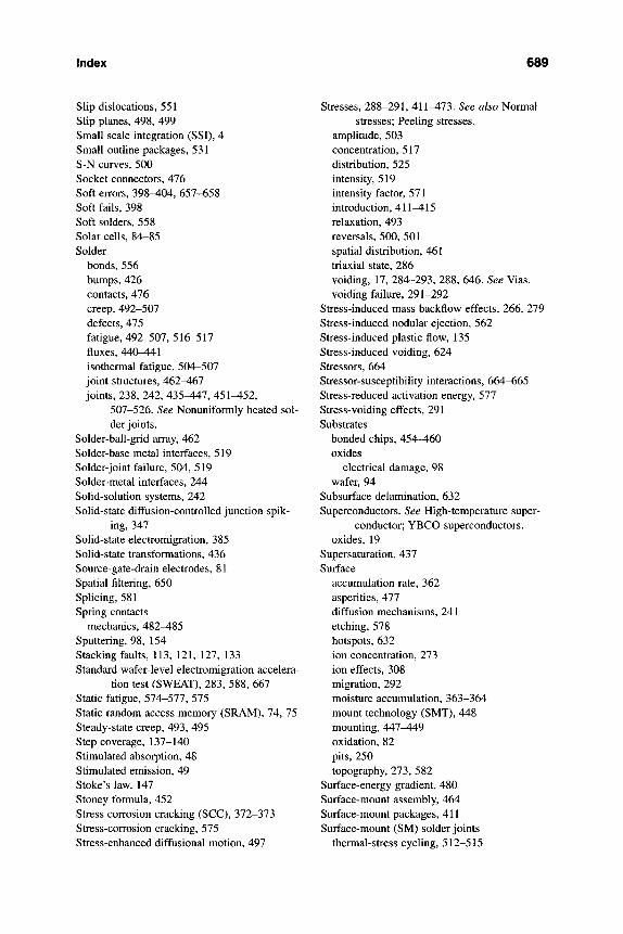
Index 689
Slip dislocations, 551 Slip planes, 498, 499 Small scale integration (SSI), 4 Small-outline packages, 531 S-N curves, 500 Socket connectors, 476 Soft errors, 398^04, 657-658 Soft fails, 398 Soft solders, 558 Solar cells, 84-85 Solder
bonds, 556 bumps, 426 contacts, 476 creep, 492-507 defects, 475 fatigue, 492-507, 516-517 fluxes, 440-441 isothermal fatigue, 504-507 joint structures, 462-467 joints, 238, 242, 435-447, 451-452,
507-526. See Nonuniformly heated sol-der joints.
Solder-ball-grid array, 462 Solder-base metal interfaces, 519 Solder-joint failure, 504, 519 Solder-metal interfaces, 244 Solid-solution systems, 242 Solid-state diffusion-controlled junction spik-
ing, 347 Solid-state electromigration, 385 Solid-state transformations, 436 Source-gate-drain electrodes, 81 Spatial filtering, 650 Splicing, 581 Spring contacts
mechanics, 482-485 Sputtering, 98, 154 Stacking faults, 113, 121, 127, 133 Standard wafer-level electromigration accelera-
tion test (SWEAT), 283, 588, 667 Static fatigue, 574-577, 575 Static random access memory (SRAM), 74, 75 Steady-state creep, 493, 495 Step coverage, 137-140 Stimulated absorption, 48 Stimulated emission, 49 Stoke's law, 147 Stoney formula, 452 Stress corrosion cracking (SCC), 372-373 Stress-corrosion cracking, 575 Stress-enhanced diffusional motion, 497
Stresses, 288-291, 411-473. See also Normal stresses; Peeling stresses.
amplitude, 503 concentration, 517 distribution, 525 intensity, 519 intensity factor, 571 introduction, 411-415 relaxation, 493 reversals, 500, 501 spatial distribution, 461 triaxial state, 286 voiding, 17, 284-293, 288, 646. See Vias. voiding failure, 291-292
Stress-induced mass backflow effects, 266, 279 Stress-induced nodular ejection, 562 Stress-induced plastic flow, 135 Stress-induced voiding, 624 Stressors, 664 Stressor-susceptibility interactions, 664-665 Stress-reduced activation energy, 577 Stress-voiding effects, 291 Substrates
bonded chips, 454-460 oxides
electrical damage, 98 wafer, 94
Subsurface delamination, 632 Superconductors. See High-temperature super-
conductor; YBCO superconductors. oxides, 19
Supersaturation, 437 Surface
accumulation rate, 362 asperities, 477 diffusion mechanisms, 241 etching, 578 hotspots, 632 ion concentration, 273 ion effects, 308 migration, 292 moisture accumulation, 363-364 mount technology (SMT), 448 mounting, AA1-AA9 oxidation, 82 pits, 250 topography, 273, 582
Surface-energy gradient, 480 Surface-mount assembly, 464 Surface-mount packages, 411 Surface-mount (SM) solder joints
thermal-stress cycling, 512-515
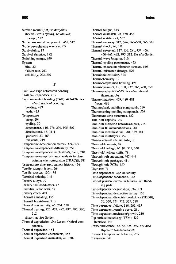
690 Index
Surface-mount (SM) solder joints thermal-stress cycling, (continued)
scope, 512 Surface-mounted components, 451, 512 Surface-roughening reaction, 579 Survivability, 17 Survival function, 182 Switching energy^ 659 System
bias, 23 failure rate, 203 reliability, 202-207
TAB. See Tape automated bonding. Tantalum capacitors, 213 Tape automated bonding (TAB), 423-426. See
also Inner lead bonding. bonding, 427 leads, 425
Temperature creep, 294 cycling, 30 dependence, 146, 276-279, 505-507 distributions, 481, 511 gradients, 23, 263 transients, 219
Temperature-acceleration factors, 324-325 Temperature-dependent diffusivity, 257 Temperature-dependent nucleation/growth, 210 Temperature-ramp resistance analysis to char-
acterize electromigration (TRACE), 281 Temperature-time-environment history, 476 Tensile strength levels, 26 Tensile stresses, 130, 136 Terminal velocity, 148 Ternary alloys, 79 Ternary semiconductors, 47 Terrestrial solar cells, 85 Tertiary creep, 494 Thermal annealing, 155 Thermal breakdown, 310 Thermal conductivity, 46, 264, 558 Thermal cychng, 427, 437, 492, 497, 507, 510,
512 distortion. See Solder.
Thermal degradation. See Lasers; Optical com-ponents.
Thermal expansion, 454 Thermal expansion coefficients, 452 Thermal expansion mismatch, 461, 507
Thermal fatigue, 415 Thermal mismatch, 28, 128, 456 Thermal resistivities, 557 Thermal runaway, 312, 564, 565-568, 566, 568 Thermal shock, 26, 511 Thermal stress(es), 127, 133, 291, 454, 456,
460-467, 492, 495, 512. See also Solder. Thermal wave imaging, 610 Thermal-cycling phenomena, 493 Thermal-expansion mismatch stresses, 556 Thermal-mismatch damage, 526 Thermionic emission, 304 Thermochemistry, 19 Thermocompression bonding, 421 Thermodynamics, 18, 108, 237, 266, 430, 659 Thermography, 630-635. See also Infrared
thermography. Thermomigration, 479, 480-481
fluxes, 480 Thermoplastic molding compounds, 599 Thermosetting molding compounds, 599 Thermostat strip structures, 452 Thin-film deposits, 142 Thin-film dielectric breakdown data, 215 Thin-film IC interconnections, 261 Thin-film metaUizations, 348, 359, 381 Thin-film multilayers, 559 Three-electrode vacuum tube, 3 Threshold currents, 89 Threshold voltage, 66, 94, 325, 330 Threshold voltage shifts, 79 Through-hole mounting, 447-449 Through-hole packages, 411 Through-hole PCBs, 450 Thyristor, 71 Time dependence. See Reliability. Time-dependent conduction, 312 Time-dependent corrosion failures. See Bond-
ing pads. Time-dependent degradation, 334, 571 Time-dependent destructive testing, 176 Time-dependent dielectric breakdown (TDDB),
70, 320, 321, 323, 325, 588 Time-dependent failure, 186, 263, 415 Time-dependent learning curve, 211 Time-dependent nucleation/growth, 210 Top surface metallurgy (TSM), 427
interface, 444 Transconductance, 72, 82, 325, 397. See also
Bipolar transconductance. Transient temperature behavior, 265 Transistors, 59
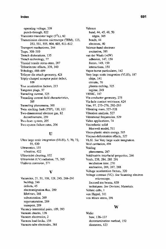
Index 691
operating voltage, 339 punch-through, 622
Transistor-transistor logic (T^L), 62 Transmission electron microscope (TEM), 123,
253, 551, 555, 604, 605, 611-612 Transport mechanisms, 244 Traps, 308-310 Trench dislocations, 135 Trench technology, 77 Triaxial tensile stress-state, 287 Triboelectric effects, 339, 340 Tribology, 488-489 Trilayer die-attach geometry, 421 Triply-charged acceptor point defect,
109 True acceleration factors, 213 Tungsten plugs, 97 Tunneling current, 325 Tunneling current-field characteristics,
305 Tunneling phenomena, 305 Twin stacking fault (TSF), 120, 121 Two-dimensional electron gas, 82
deconfinement, 259 Two-laser system, 205 Two-system failure rates, 206
u Ultra large scale integration (ULSI), 5, 70, 72,
95, 630 Ultrasonics, 151
vibration, 422 Ultraviolet cleaning, 152 Ultraviolet (UV) radiation, 75, 395 Uniform corrosion, 371
Vacancies, 21, 51, 108, 121, 245, 288-291 buildup, 246 defects, 45 electromigration flux, 289 lifetimes, 268 subsaturation, 269 supersaturation, 269 transport, 289
Vacancy-interstitial pairs, 109, 393 Vacuum chucks, 136 Vacuum electronics, 2 Vacuum load-locks, 154 Vacuum-tube electrodes, 381
Valence band, 44, 45, 48, 50
edges, 305 bonds, 44 electrons, 40
Valence-band electrons excitation, 395
van der Waals (vdW) adhesion, 147, 150 forces, 149, 150 interactions, 151
Vapor-borne particulates, 142 Very large scale integration (VLSI), 187
chips, 141 circuits, 70 plasma etching, 325 regime, 249
VHSIC, 187 Via-conductor geometry, 275 Via-hole contact resistance, 624 Vias, 97, 275-276, 292-293 Vibrating mass, 527-528 Vibration analysis, 527 Vibrational frequencies, 529 Video applications, 74 Viscoelastic solid
Maxwell model, 511 Visco-plastic strain energy, 515 Viscous-deformation effects, 527 VLSI. See Very large scale integration. Void cavitation, 494 Voiding
phenomena, 267 Void/matrix interfacial properties, 246 Voids, 238, 284, 288-291
incubation time, 270 nucleation, 269, 287, 288
Voltage acceleration factors, 320 Voltage contrast (VC). See Scanning electron
microscope. focused ion beams, 630 techniques. See Devices; Materials.
Voltaic cells, 1 von Hippel, 311 von Mises stress, 291
w Wafer
bow, 136-137 decontamination method, 152 diameters, 123
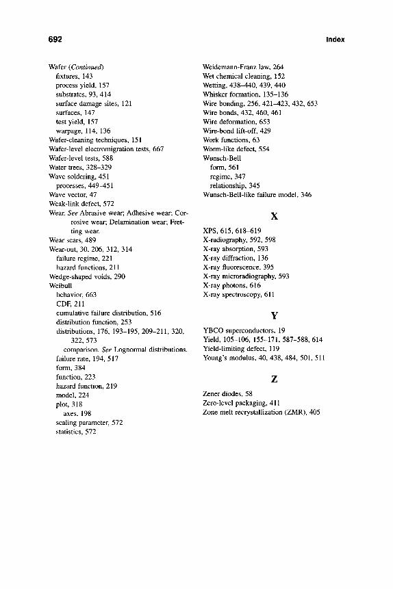
692 Index
Wafer (Continued) fixtures, 143 process yield, 157 substrates, 93, 414 surface damage sites, 121 surfaces, 147 test yield, 157 warpage, 114, 136
Wafer-cleaning techniques, 151 Wafer-level electromigration tests, 667 Wafer-level tests, 588 Water trees, 328-329 Wave soldering, 451
processes, 449-451 Wave vector, 47 Weak-link defect, 572 Wear. See Abrasive wear; Adhesive weeir; Cor-
rosive wear; Delamination wear; Fret-ting wear.
Wear scars, 489 Wear-out, 30, 206, 312, 314
failure regime, 221 hazard functions, 211
Wedge-shaped voids, 290 WeibuU
behavior, 663 CDF, 211 cumulative failure distribution, 516 distribution function, 253 distributions, 176, 193-195, 209-211, 320,
322, 573 comparison. See Lognormal distributions.
failure rate, 194,517 form, 384 function, 223 hazard function, 219 model, 224 plot, 318
axes, 198 scaling parameter, 572 statistics, 572
Weidemann-Franz law, 264 Wet chemical cleaning, 152 Wetting, 438-UO, 439, 440 Whisker formation, 135-136 Wire bonding, 256, 421-423, 432, 653 Wire bonds, 432, 460, 461 Wire deformation, 653 Wire-bond lift-off, 429 Work functions, 63 Worm-like defect, 554 Wunsch-Bell
form, 561 regime, 347 relationship, 345
Wunsch-Bell-like failure model, 346
XPS, 615, 618-619 X-radiography, 592, 598 X-ray absorption, 593 X-ray diffraction, 136 X-ray fluorescence, 395 X-ray microradiography, 593 X-ray photons, 616 X-ray spectroscopy, 611
YBCO superconductors, 19 Yield, 105-106, 155-171, 587-588, 614 Yield-limiting defect, 119 Young's modulus, 40, 438, 484, 501, 511
Zener diodes, 58 Zero-level packaging, 411 Zone melt recrystallization (ZMR), 405