Reliability Experience - Computer Action Teamweb.cecs.pdx.edu/~cgshirl/Documents/QRE_ECE510... ·...
95
1 Reliability Experience Bill Roesch (Rush) TriQuint Fellow, Reliability Science (503) 615-9292 [email protected]
Transcript of Reliability Experience - Computer Action Teamweb.cecs.pdx.edu/~cgshirl/Documents/QRE_ECE510... ·...

1
Reliability
Experience
Bill Roesch (Rush) TriQuint Fellow, Reliability Science
(503) 615-9292

2
Purposes:
Increase Your Reliability Knowledge Base. (Share Experience)
Answer Questions
About Reliability.
2
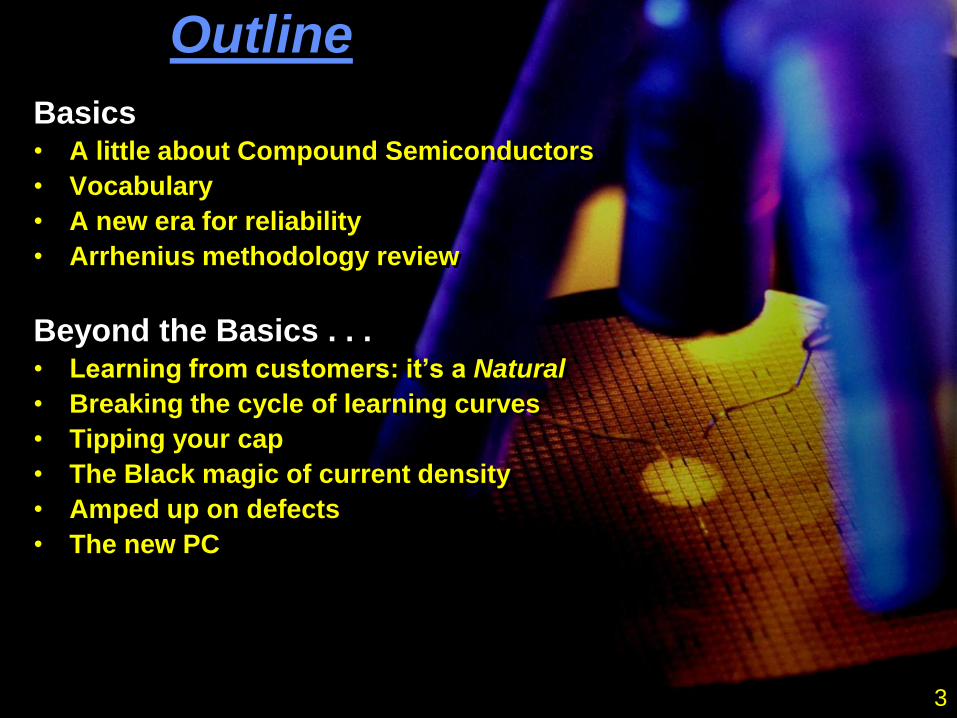
Outline
3
Basics
• A little about Compound Semiconductors
• Vocabulary
• A new era for reliability
• Arrhenius methodology review
Beyond the Basics . . . • Learning from customers: it’s a Natural
• Breaking the cycle of learning curves
• Tipping your cap
• The Black magic of current density
• Amped up on defects
• The new PC

4
Why GaAs Reliability?
• Volume drives reliability.
• GaAs is different than silicon.
• New compounds (GaN) have more to go.
“Reliability counts.
In almost every case integrated electronics
has demonstrated high reliability.”
Gordon Moore, Electronics Magazine, 1965.
Cramming more components onto integrated circuits
4 of 50
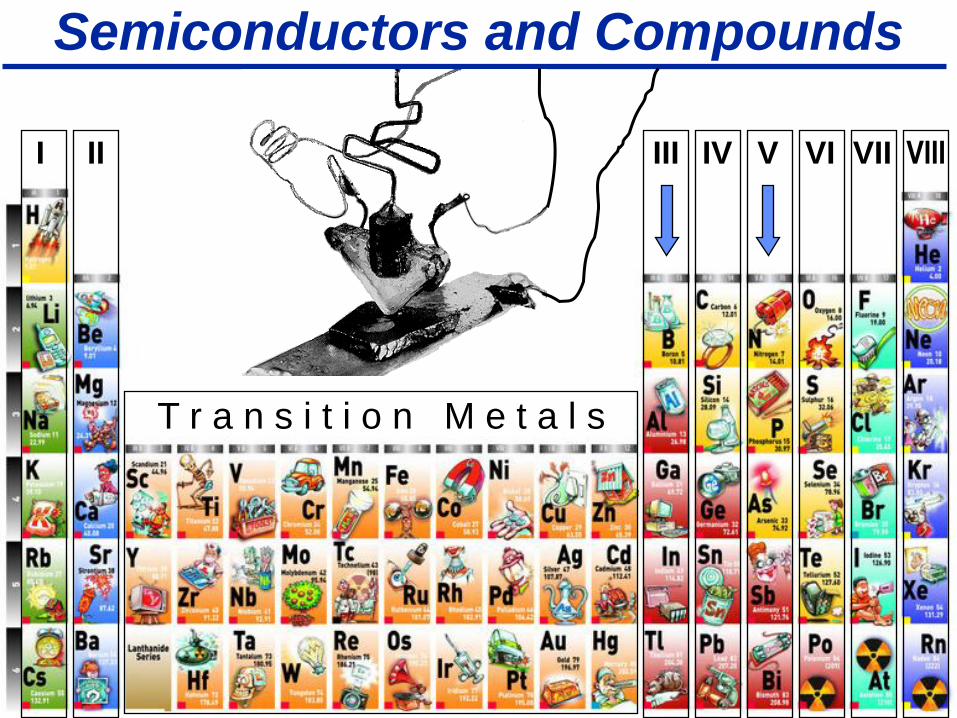
5
I II III IV V VI VII VIII
T r a n s i t i o n M e t a l s
Semiconductors and Compounds

6
Contrasting Improvement Methods 1. No significant historical improvement in lifetimes.
Performance Reliability Yield Focus
Si Shrink Physical
Size New Materials Defects
C.S. New
Materials Don’t Shrink (Good Enough)
Parametric
See for yourself – Check out the International
Technology Roadmap for Semiconductors.
There is an RF for wireless communications chapter!
2. Moore’s Law doesn’t exactly apply to Compound Semiconductors.
6 of 50

7
Choosing Materials
“Silicon is likely to remain the basic material, although
others will be of use in specific applications. For
example, gallium arsenide will be important in
integrated microwave functions.”
Gordon Moore, Electronics Magazine, 1965.
Cramming more components onto integrated circuits

8
What’s so great about GaAs?
Direct Gap, Low Electron Effective Mass
Perfect for LEDs & Solar Cells
High Speed Electrons
9
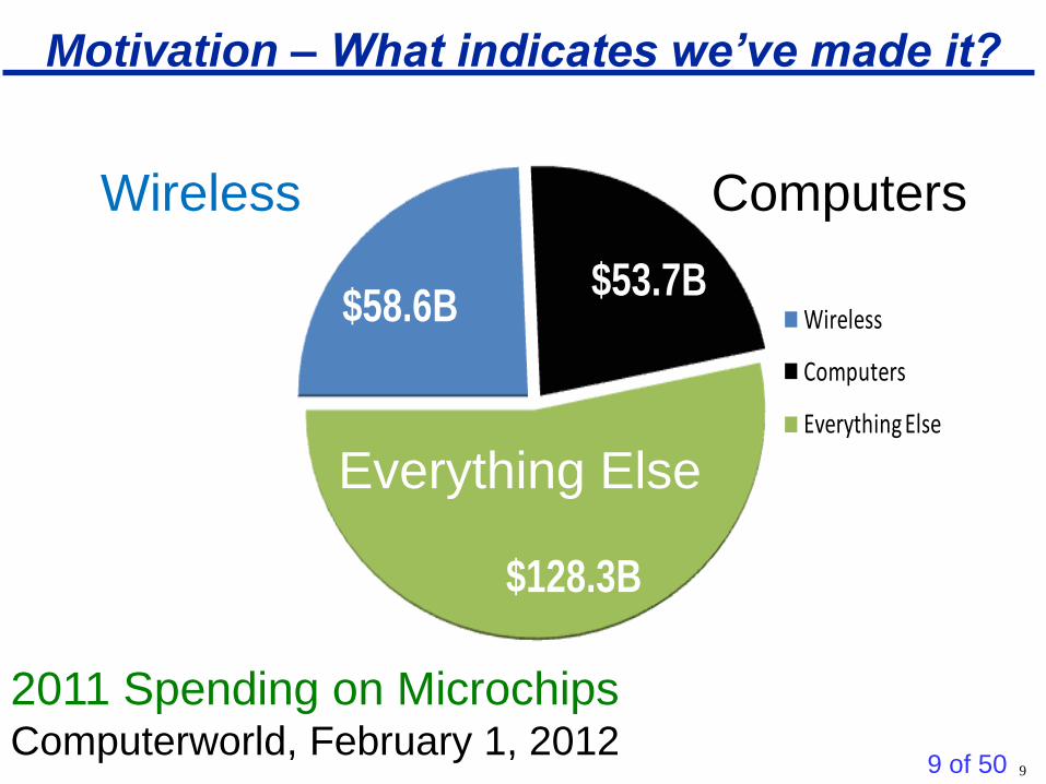
Motivation – What indicates we’ve made it?
$58.6B$53.7B
$128.3B
Wireless
Computers
Everything Else
2011 Spending on Microchips Computerworld, February 1, 2012
Wireless Computers
Everything Else
9 of 50

Vocabulary – What is an RF Product?
11
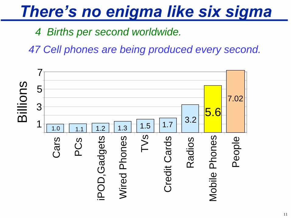
There’s no enigma like six sigma
47 Cell phones are being produced every second.
5.6
4 Births per second worldwide.
1.3 1.5 1.2 1.1 1.0 1.7
3.2 5.6
1
3
5
7
Cars
PC
s
iPO
D,G
adg
ets
Wired
Ph
on
es
Cre
dit C
ard
s
TV
s
Radio
s
Mobile
Phon
es
Pe
op
le
Bill
ions
7.02
12
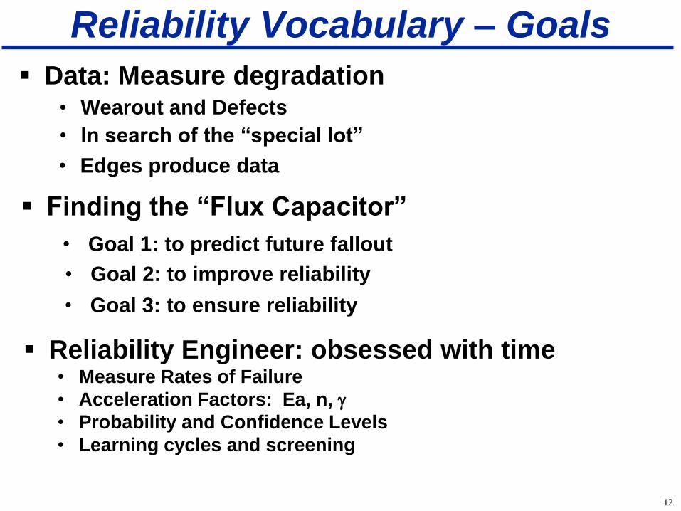
Reliability Vocabulary – Goals
Data: Measure degradation
Finding the “Flux Capacitor”
• In search of the “special lot”
• Edges produce data
• Goal 1: to predict future fallout
• Goal 2: to improve reliability
• Goal 3: to ensure reliability
• Wearout and Defects
Reliability Engineer: obsessed with time • Measure Rates of Failure
• Acceleration Factors: Ea, n, g
• Probability and Confidence Levels
• Learning cycles and screening
13
Success
Testing
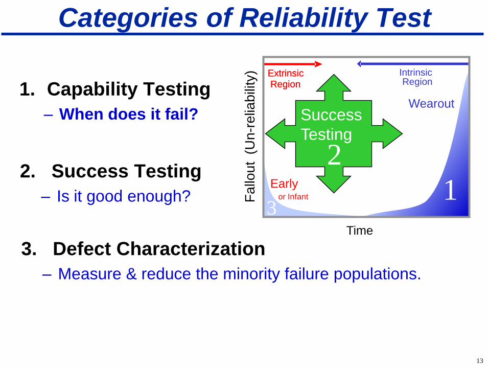
Categories of Reliability Test
1. Capability Testing
– When does it fail?
Time
Wearout
Extrinsic
Region
Intrinsic Region
Fa
llou
t (
Un-r
elia
bili
ty)
Early or Infant
Extrinsic
Region
1 3
2. Success Testing
– Is it good enough?
3. Defect Characterization
– Measure & reduce the minority failure populations.
2
14
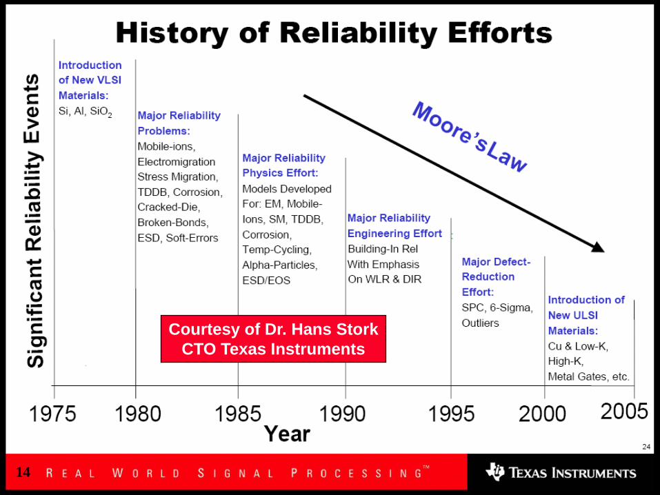
Courtesy of Dr. Hans Stork
CTO Texas Instruments
14

15
Historical Eras of Reliability
Era Definition VLSI Silicon Example Compound Semi
1 Materials 1975 Materials: Si, Al, SiO2 1980 GaAs, Au, SixNx
2 Mechanisms (Major Reliability
Problems)
1980 Mobile-ions, E-M,
S-M, TDDB, Corrosion,
Cracked-Die, ESD, Soft-
Errors
1985 Sinking Gates,
Ohmic Contacts
3 Physics
(Major Reliability
Physics Effort)
1985 Models… EM, Mobile-Ions, SM, TDDB,
Corrosion, Temp-Cycling,
Alpha Particles, EOS/ESD
1990 Models… Thermal Diffusion,
JEP118, Hydrogen
4 Engineering (Major Reliability
Engineering Effort)
1990 Building-In Reliability, with
Emphasis on WLR & DIR
1995 WLR, Passives, BIR
5 Defects
(Major Defect-
Reduction Effort)
1995 SPC & 6 Sigma Outliers
2000 Capacitors,
Interconnects

16
Outline
Basics
• A little about Compound Semiconductors
• Vocabulary
• A new era for reliability
• Arrhenius methodology review
Beyond the Basics . . .
• Learning from customers: it’s a Natural
• Breaking the cycle of learning curves
• Tipping your cap
• The Black magic of current density
• Amped up on defects
• The new PC

17
How to Accelerate?
Temperature Current Humidity Voltage
Mech. Stress Contaminants
Radiation Electric Fields
Force Power
Pressure Light
How long does reliability qualification really take?
These
are the
reliability
engineer’s
tools

18
Arrhenius: Godfather of Reliability
Time To Fail = exp[Ea/k(1/Temp)] Ea = Activation Energy (in eV = “Electron Volts”), k = Boltzman’s Constant
Graphical analysis using log time and 1/temperature
grid to reveal thermal acceleration factor.
19
FET Technology Primary Wearout Mechanism
• No Gate Oxide.
• Reliable, Recessed, Schottky Gate. Not MOS!
• Less Susceptible to Surface Effects.
• No Ionic Contamination.
• Relatively Short Process Flow.

20
FET Degradation Distribution
12 Samples out of 24 FETs
Actual Data: notice time to reach 20%
reduction in channel current.

21
245ºC FET Distribution
These are individual FET times to
failure plotted on a lognormal grid.

22
FET Distributions
Distributions for the same population
aged at five different temperatures.
23
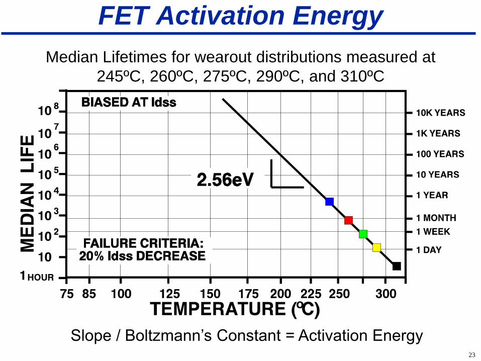
FET Activation Energy
Median Lifetimes for wearout distributions measured at
245ºC, 260ºC, 275ºC, 290ºC, and 310ºC
Slope / Boltzmann’s Constant = Activation Energy
24
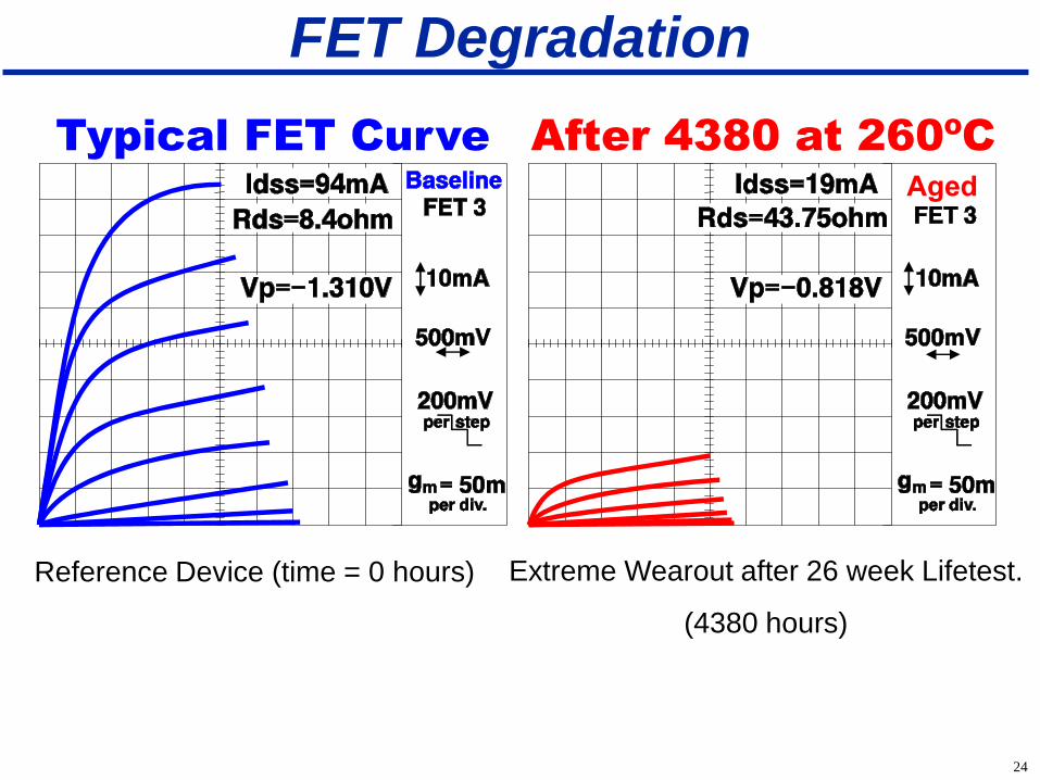
FET Degradation
Reference Device (time = 0 hours) Extreme Wearout after 26 week Lifetest.
(4380 hours)
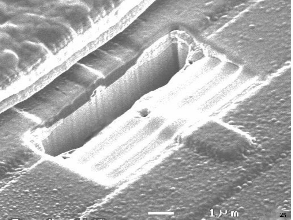
25 25

26 26
27
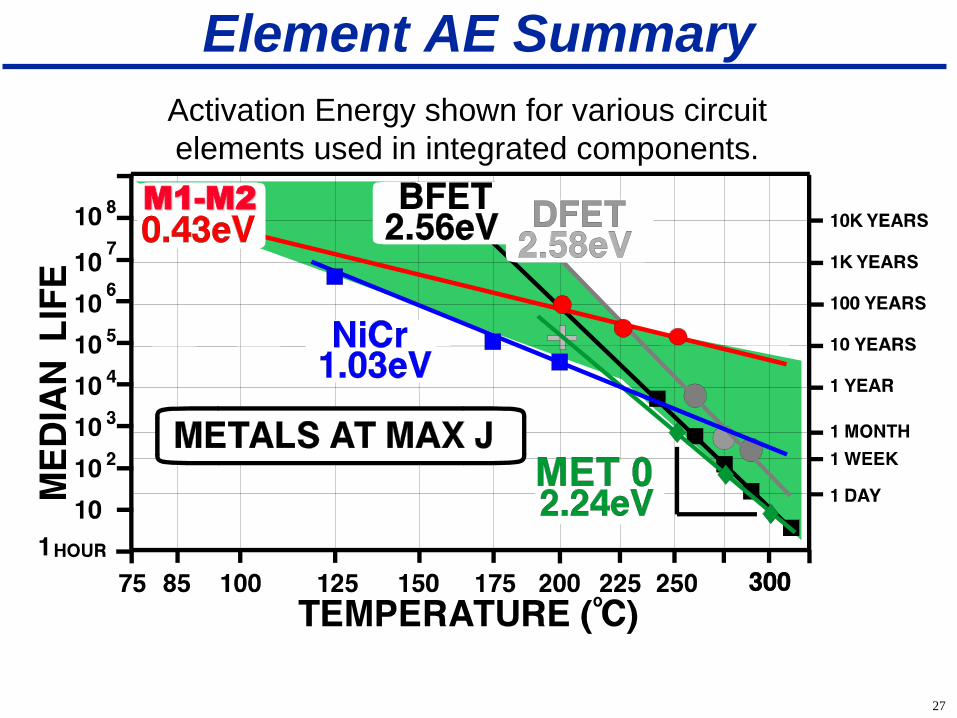
Element AE Summary
M1-M2
Activation Energy shown for various circuit
elements used in integrated components.

28
Long Term Trend for pHEMT

Basics Review Basics
• Vocabulary: Reliability is the duration of quality – We’re headed the same direction, just different words for it.
• A new era for reliability: Improvement follows a progression – The path to improvement is well travelled.
– Compound Semiconductors don’t obey Moore’s law.
– One man’s trash is a reliability man’s treasure.
• Arrhenius methodology review: Time to move beyond temperature
High
Temperature
WEAROUT
VOLUME
QUALITY
YIELD
DEFECTS
“I think I dropped my car
keys over there, but let’s look
here because the light is
much better.” 29
– We have to stop looking where the light seems to better.
• Are we doomed to repeat history? We know where we’ve been.

30
Outline
Basics
• A little about Compound Semiconductors
• Vocabulary
• A new era for reliability
• Arrhenius methodology review
Beyond the Basics . . .
• Learning from customers: it’s a Natural
• Breaking the cycle of learning curves
• Tipping your cap
• The Black magic of current density
• Amped up on defects
• The new PC
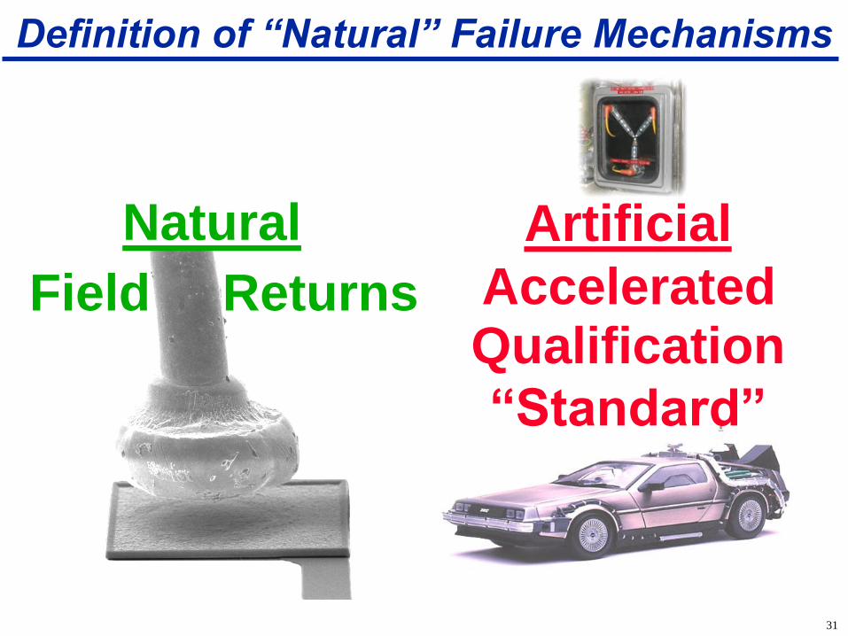
31
Natural
Field Returns
Artificial
Accelerated
Qualification
“Standard”
Definition of “Natural” Failure Mechanisms
32
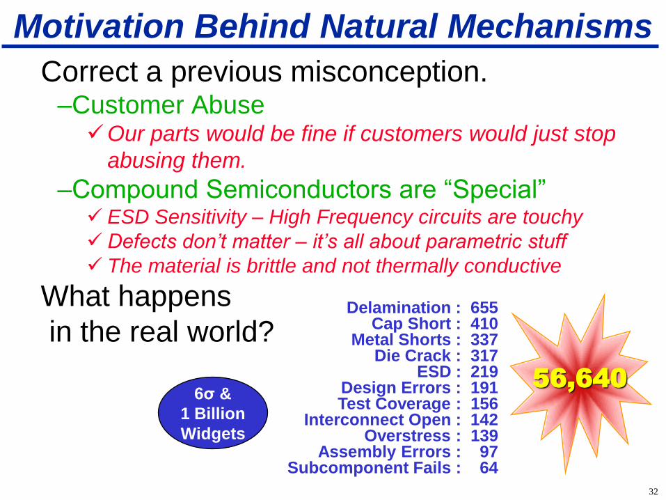
Correct a previous misconception. –Customer Abuse Our parts would be fine if customers would just stop
abusing them.
–Compound Semiconductors are “Special” ESD Sensitivity – High Frequency circuits are touchy
Defects don’t matter – it’s all about parametric stuff
The material is brittle and not thermally conductive
What happens
in the real world?
56,640
Delamination : 655 Cap Short : 410
Metal Shorts : 337 Die Crack : 317
ESD : 219 Design Errors : 191 Test Coverage : 156
Interconnect Open : 142 Overstress : 139
Assembly Errors : 97 Subcomponent Fails : 64
6σ &
1 Billion
Widgets
Motivation Behind Natural Mechanisms
33
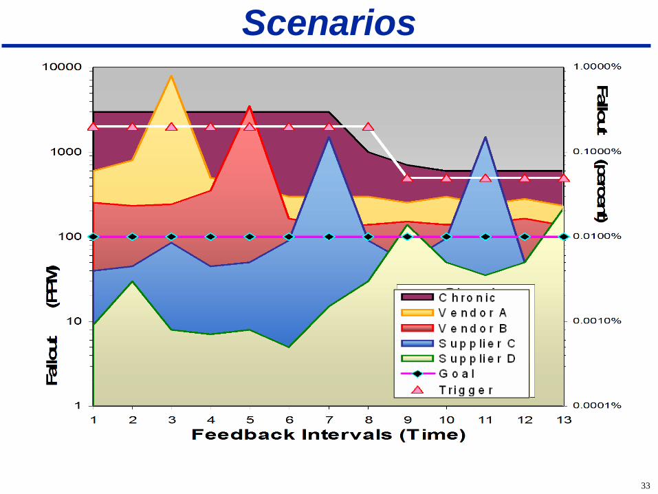
Scenarios

34
Customer
Category
RF Product
Type Volume
Claimed
Trigger Actual Trigger
Automotive PA Low > zero Every Failure
Standard
Product Various Large 100 DPM 100-2000 DPM
Cell Phone PA High 100 DPM 200-2000 DPM
Cell Phone RF High 100 DPM 20,000 DPM
Long Haul Digital Medium 100 DPM 20,000 DPM
PC/LAN LNA High 200 DPM 20,000 DPM
Cell Phone PA High 40 DPM 50,000 DPM
Levels Triggering Returns
35
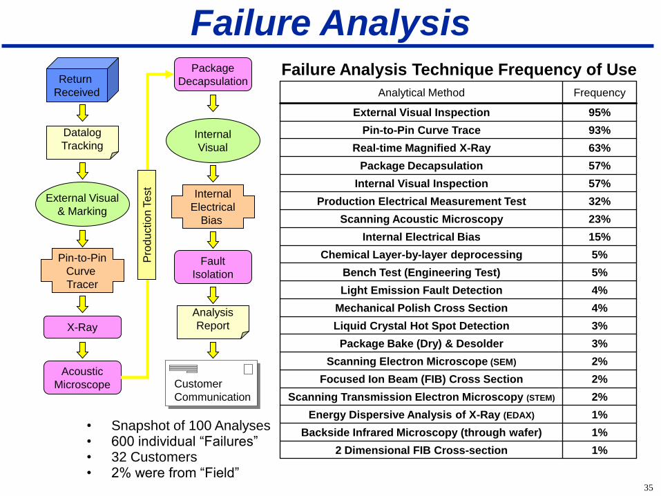
Failure Analysis Technique Frequency of Use
1% 2 Dimensional FIB Cross-section
1% Backside Infrared Microscopy (through wafer)
1% Energy Dispersive Analysis of X-Ray (EDAX)
2% Scanning Transmission Electron Microscopy (STEM)
2% Focused Ion Beam (FIB) Cross Section
2% Scanning Electron Microscope (SEM)
3% Package Bake (Dry) & Desolder
3% Liquid Crystal Hot Spot Detection
4% Mechanical Polish Cross Section
4% Light Emission Fault Detection
5% Bench Test (Engineering Test)
5% Chemical Layer-by-layer deprocessing
15% Internal Electrical Bias
23% Scanning Acoustic Microscopy
32% Production Electrical Measurement Test
57% Internal Visual Inspection
57% Package Decapsulation
63% Real-time Magnified X-Ray
93% Pin-to-Pin Curve Trace
95% External Visual Inspection
Frequency Analytical Method
Return
Received
Datalog
Tracking
External Visual
& Marking
Pin-to-Pin
Curve
Tracer
X-Ray
Acoustic
Microscope
Package
Decapsulation
Internal
Visual
Internal
Electrical
Bias
Analysis
Report
Customer
Communication
Fault
Isolation
Pro
du
ctio
n T
est
Failure Analysis
• Snapshot of 100 Analyses • 600 individual “Failures” • 32 Customers • 2% were from “Field”

36
►Electrical Overstress
►Thermal Overstress
►Mechanical Overstress
►Assembly & Packaging
►No Fault Found
►Design
►Test
►Others
►Defects
Natural Mechanism Examples
36

37
De
sig
n 3%
Test Issue
9%No Fault
Found
33%
Assembly/
Packaging
Issues
13%
Fab
Process
Defect
18%
EOS/ESD
24%
Design
Issue
4%Fab
Process
Defect
32%
Assembly/
Packaging
Issues
19%
No Fault
Found
19%
Test Issue
7%
EOS/ESD
19%
Test
Issue
3%
Design
Issue 4%
Untestable 3%
No Fault
Found
20%
Application
42%
EOS/ESD
28%
1985-1992
1999-2004
2005-2006
Evolution of Natural Failure Mechanisms
38
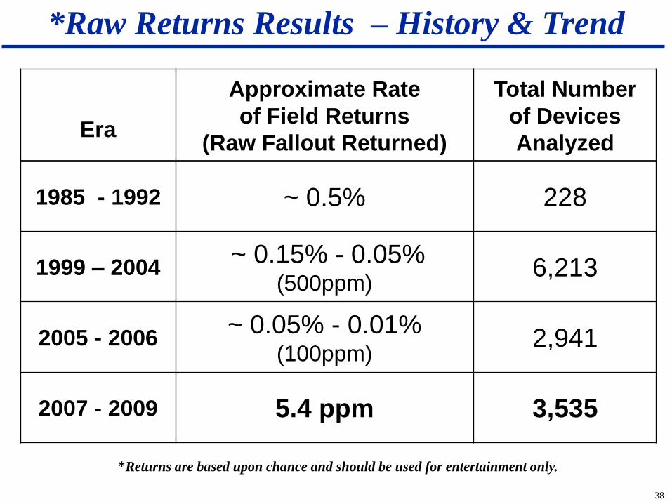
Era
Approximate Rate
of Field Returns
(Raw Fallout Returned)
Total Number
of Devices
Analyzed
1985 - 1992 ~ 0.5% 228
1999 – 2004 ~ 0.15% - 0.05%
(500ppm) 6,213
2005 - 2006 ~ 0.05% - 0.01%
(100ppm) 2,941
2007 - 2009 5.4 ppm 3,535
*Raw Returns Results – History & Trend
*Returns are based upon chance and should be used for entertainment only.
39
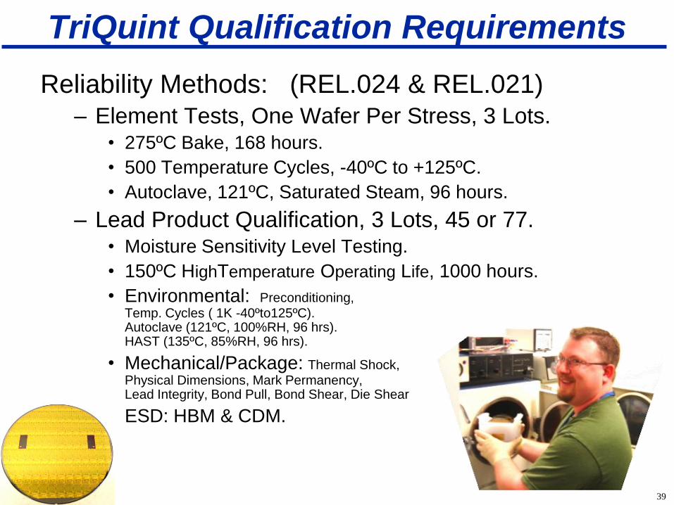
TriQuint Qualification Requirements
Reliability Methods: (REL.024 & REL.021) – Element Tests, One Wafer Per Stress, 3 Lots.
• 275ºC Bake, 168 hours.
• 500 Temperature Cycles, -40ºC to +125ºC.
• Autoclave, 121ºC, Saturated Steam, 96 hours.
– Lead Product Qualification, 3 Lots, 45 or 77. • Moisture Sensitivity Level Testing.
• 150ºC HighTemperature Operating Life, 1000 hours.
• Environmental: Preconditioning, Temp. Cycles ( 1K -40ºto125ºC). Autoclave (121ºC, 100%RH, 96 hrs). HAST (135ºC, 85%RH, 96 hrs).
• Mechanical/Package: Thermal Shock, Physical Dimensions, Mark Permanency, Lead Integrity, Bond Pull, Bond Shear, Die Shear
• ESD: HBM & CDM.
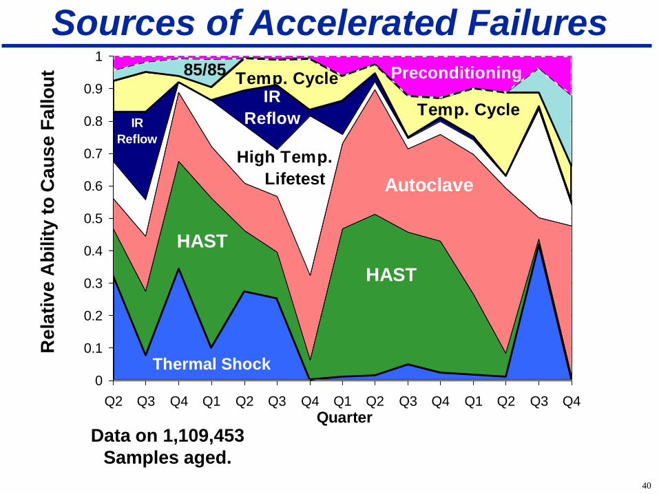
40
0
0.1
0.2
0.3
0.4
0.5
0.6
0.7
0.8
0.9
1
Q2 Q3 Q4 Q1 Q2 Q3 Q4 Q1 Q2 Q3 Q4 Q1 Q2 Q3 Q4
Quarter
Re
lati
ve
Ab
ilit
y t
o C
au
se
Fa
llo
ut
HAST
Autoclave
High Temp.
Lifetest
IR
Reflow
Temp. Cycle85/85 Preconditioning
IR
Reflow
Temp. Cycle
HAST
Data on 1,109,453
Samples aged.
Sources of Accelerated Failures
Thermal Shock

41
Cap Short
15%
Metal Short
12%
Die Crack
12%
ESD
8%
Design Error
7%
Test Coverage
5%
Inteconnect
Open
5%
Overstress
5%
Assembly Error
5%
Subcomponent
Fails
2%
Delamination
24%
Natural
Accelerated
Comparisons – A snapshot
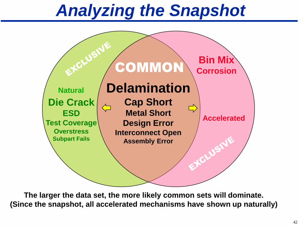
42
Natural
Accelerated
COMMON
Delamination Cap Short Metal Short
Design Error Interconnect Open
Assembly Error
Bin Mix Corrosion
Die Crack ESD
Test Coverage Overstress Subpart Fails
Analyzing the Snapshot
The larger the data set, the more likely common sets will dominate.
(Since the snapshot, all accelerated mechanisms have shown up naturally)
43
• Customer data is the best we can get, but it’s not perfect
– Lack of returns should not be interpreted as a lack of failures
• Findings are not static, they change over time
• Focus on exclusive mechanisms (both sides)
• Natural is a sanity check on accelerated
• Natural is reactive, but only if you react
• Breaking through the improvement cycle
Value of Investigating Natural FMs

44
Outline
Basics
• A little about Compound Semiconductors
• Vocabulary
• A new era for reliability
• Arrhenius methodology review
Beyond the Basics . . .
• Learning from customers: it’s a Natural
• Breaking the cycle of learning curves
• Tipping your cap
• The Black magic of current density
• Amped up on defects
• The new PC

45
C.I. = Early RF Product Fallout Data
W.Roesch, “Getting to Zero, Methods of Reducing Defects,”
GaAs REL Workshop, pp. 37-46, 2001
1
10
100
1000
10000
100000
99Q1 99Q2 99Q3 99Q4 00Q1 00Q2 00Q3 00Q4 01Q1 01Q2
Fiscal Quarter
De
fec
ts P
er
Milli
on
Customer-Measured Defects (DPM)
Outgoing Sample Defects (DPM)
Volume ramp on MESFET phone receivers.
2 Years

46
Working With a Customer
• We send a million parts.
Fix Process Defect.
Redesign & improve ESD Performance.
Customer finds ESD Source.
Fix Another Process Defect.
Beware of the desk drawer syndrome.
• They return 19.
• We re-test, and 13 pass.
• We perform FA on 6.
• Find 3 process defects.
• Result ~ 3 DPM.
• Corrective Action.
• Start Over.

47
Historical Product/Reliability Cycle
2000 WorkWeek 2008 1
10
100
1000
10000
Defe
cts
P
er
Mill
ion
Integrated
RF Receiver 1st Gen
PA Module
2st Gen
PA Module
Transmit
Module
PA Switch Filter Module
Supplier outgoing quality sample Customer Factory Data
48
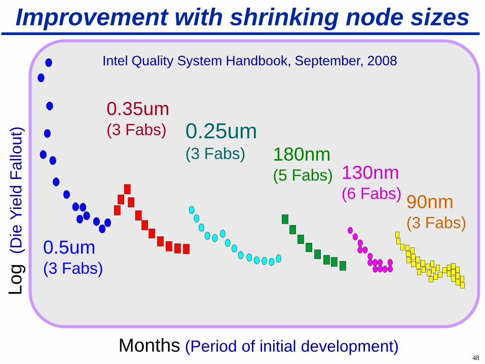
Improvement with shrinking node sizes
Intel Quality System Handbook, September, 2008
Months (Period of initial development)
Lo
g
(Die
Yie
ld F
allo
ut)
0.5um (3 Fabs)
0.35um (3 Fabs) 0.25um
(3 Fabs)
130nm (6 Fabs)
180nm (5 Fabs)
90nm (3 Fabs)

49
RF Outrunning
the Bear
50
Outline
Basics
• A little about Compound Semiconductors
• Vocabulary
• A new era for reliability
• Arrhenius methodology review
Beyond the Basics . . .
• Learning from customers: it’s a Natural
• Breaking the cycle of learning curves
• Tipping your cap
• The Black magic of current density
• Amped up on defects
• The new PC
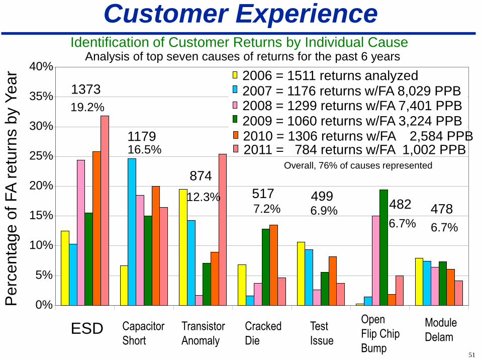
51
0%
5%
10%
15%
20%
25%
30%
35%
40%
ESD Capacitor
Short
Transistor
Anomaly
Cracked
Die
Test
Issue
Open
Flip Chip
Bump
Module
Delam
2006 = 1511 returns analyzed
2007 = 1176 returns w/FA 8,029 PPB 2008 = 1299 returns w/FA 7,401 PPB
2009 = 1060 returns w/FA 3,224 PPB 2010 = 1306 returns w/FA 2,584 PPB
2011 = 784 returns w/FA 1,002 PPB
1373
1179
874
517 499 482 478
19.2%
16.5%
12.3% 7.2% 6.9%
6.7% 6.7%
Overall, 76% of causes represented
Customer Experience Identification of Customer Returns by Individual Cause
Analysis of top seven causes of returns for the past 6 years
Perc
enta
ge o
f FA
retu
rns b
y Y
ear

52
Planarizing dielectric (BCB)
Overlaying Dielectric
Capacitor Dielectric
Capacitor Construction – Sources of Variation
All defects underneath and coincident with the Metal Zero layer
can affect the integrity of the capacitor. These “defects” and
anomalies in the dielectric layer can be considered as a variation
in the dielectric thickness.
Underlying dielectric layers
Capacitor Bottom Plate (Metal 0)
Capacitor Top Plate (MIM Metal)
Plated Gold Interconnect
Metal 1
Via 1
Wafer Substrate
Capacitors

53 1300pF/mm2
Capacitor Test Structures
10K
μm2
5K
μm2
1K
μm2
800K μm2
400K μm2 200K μm2
100Kμm2 50K
μm2
25K
μm2
54
Ord
ere
d C
ap
acito
r D
ata
0
10
20
30
40
50
60
70
80
90
100
110
Voltage Ramp: Destructive Test
Intrinsic capacitor
population
(Good Capacitors)
Extrinsic capacitor
population
(Defect-driven)
25KCap Capacitor Fail Voltage
0 5 10 15 20 25 30 35 40 45 50 55 60
Process Variation
Defect Density
55
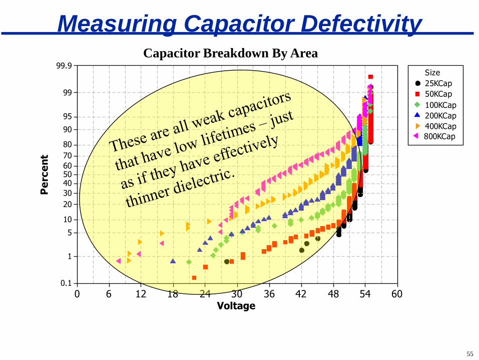
Measuring Capacitor Defectivity
6 0 5 4 4 8 4 2 3 6 3 0 2 4 1 8 1 2 6 0
9 9 . 9
9 9
9 5
9 0
8 0
7 0
6 0 5 0 4 0
3 0
2 0
1 0
5
1
0 . 1
Voltage
P e
r c e
n t
2 5 K C a p
1 0 0 K C a p
2 0 0 K C a p
4 0 0 K C a p
S i z e
5 0 K C a p
8 0 0 K C a p
Capacitor Breakdown By Area

56
Example of a Capacitor Short due to a Defect The capacitor is cross-
sectioned at the solid red line
MET0 – Capacitor Bottom Plate
MIM – Top Plate
Defect
The defect is a metal filament lying on top of the capacitor bottom plate
Capacitor
Dielectric
PR
LA BD
GaAs

57
Relative Resolution of Electrical Detection Methods
Full population
characteristics determined
. by ramp-to-breakdown
testing. (Black is unstressed)
This is a 99% defective population!
3-6V Module FT (100%)
20V Die Sort (100%)
Duration
Duration
Module Litmus Sample 20- 80
10-3% LTPD
Wafer Litmus Sample 8- 22
30-10% LTPD
1-12hr
8.5min
Breakdown Voltage (Volts) 500Å Dielectric Cap
Not Detectible by Low Voltage Stress
Not Detectible by Moderate Voltage
Sam
ple
Siz
e R
eso
luti
on
.
Voltage Resolution

58
Outline
Basics
• A little about Compound Semiconductors
• Vocabulary
• A new era for reliability
• Arrhenius methodology review
Beyond the Basics . . .
• Learning from customers: it’s a Natural
• Breaking the cycle of learning curves
• Tipping your cap
• The Black magic of current density
• Amped up on defects
• The new PC
59
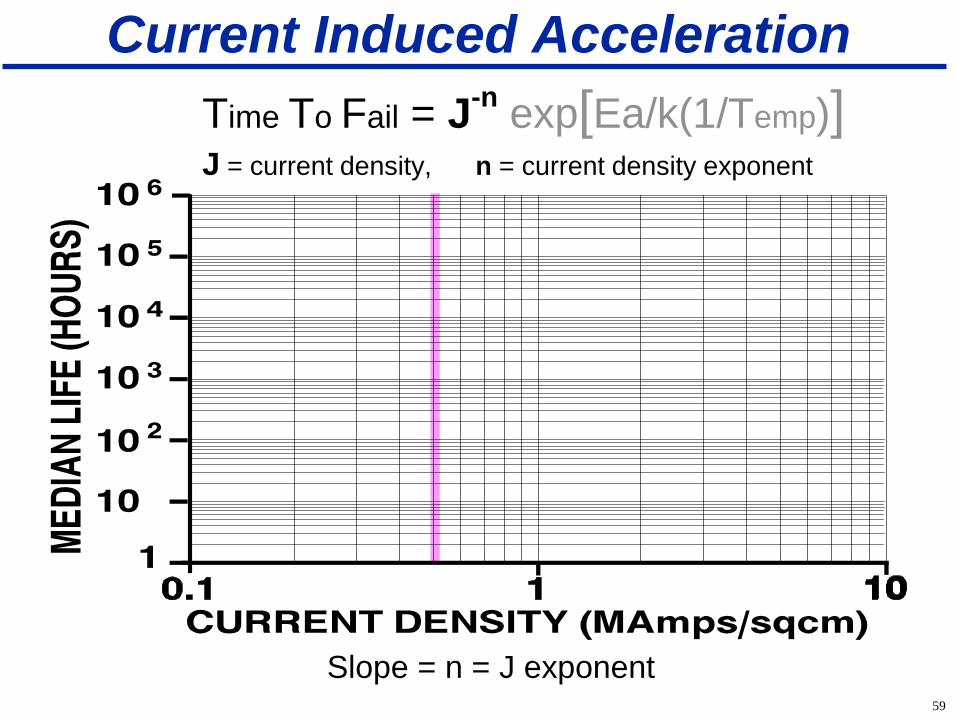
Current Induced Acceleration
Time To Fail = J-n
exp[Ea/k(1/Temp)] J = current density, n = current density exponent
Slope = n = J exponent

60
How to get > 1 Million Amps?
Interpreting these conditions
is problematic because the “standard” user environment is not easily predictable . . .
and because the factors of Stress, Current, and Voltage are almost always confounded with Temperature.
60

61
Summary of current density acceleration
factors for various circuit elements.
M0
M1-M2
J Exponent Summary

62
Plated Gold Activation Energy

63
Outline
Basics
• A little about Compound Semiconductors
• Vocabulary
• A new era for reliability
• Arrhenius methodology review
Beyond the Basics . . .
• Learning from customers: it’s a Natural
• Breaking the cycle of learning curves
• Tipping your cap
• The Black magic of current density
• Amped up on defects
• The new PC

64
In Q1 2004,
process
defects
became the
leading
cause of
failure for
field returns
at TriQuint
Oregon.
0%
10%
20%
30%
40%
50%
60%
70%
80%
90%
100%
01Q1 01Q2 01Q3 01Q4 02q1 02q2 02q3 02q4 03Q1 03Q2 03Q3 03Q4 04q1 04q2
Pe
rce
nt
of
Fa
ilu
res
An
aly
ze
d
Design or Application Issues
Process Defect
EOS/ESD Test
Issue
No Fault Found (Good)
Yearly Reporting Quarter
Root Causes of Field Returns

65
Non-thermal Acceleration Example
Early Wearout
Time (arbitrary units)
Failu
re R
ate
(a
rbitra
ry u
nits)
Finding Early or Infant Failure
Mechanisms is a challenge for
the Reliability Engineer.
Leakage
Voltage
Spacing
Defects Amp
Defect Amplification
66
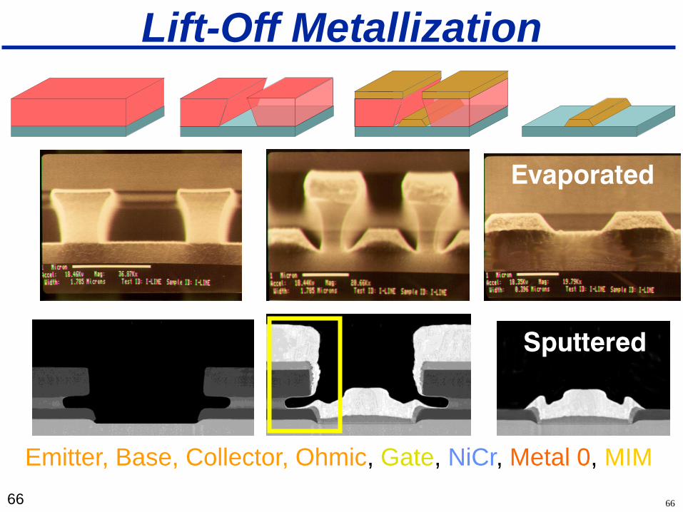
Lift-Off Metallization
Emitter, Base, Collector, Ohmic, Gate, NiCr, Metal 0, MIM
66
Sputtered
Evaporated
67
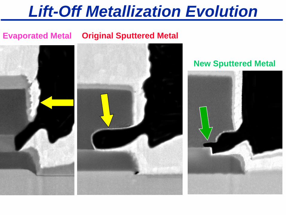
Evaporated Metal Original Sputtered Metal
Original Sputtered Metal
New Sputtered Metal
New Sputtered Metal
Lift-Off Metallization Evolution

Gap
Interdigitated Fingers.
1880um Periphery.
One leakage across.
Comb
Pair of folded traces “meandering”. . .
diagonally, horizontally, & vertically.
30mm Periphery.
Leakage between traces.
Resistance of each trace.
Meander
Gap in solid
rectangle.
1350um
Periphery.
One leakage
across.
68 68

69
How to “amplify” low level defects:
Comb Style Structure.
Unknown?
Testable Electrically: Apply Voltage, Measure Leakage
Quality Concerns
(Always Shorted)
Yield Loss
Reliability
Concerns
(Near Shorts)
70
0
10
20
30
40
50
60
70
80
90
100
Spacing Between Metals ( Approximate 100 nm Units)
Test
Str
uctu
re Q
uality
Level (%
)
Approach
Guardband
Layout
Limit
DEFECT AMPLIFICATION
70

71
Yield as a Function of Spacing
y = 3.4886x + 95.088
R2 = 0.9983
84
86
88
90
92
94
96
98
100
0.5 1 1.5 2 2.5
Space Between Adjacent Metals (micron)
Yie
ld a
t Z
ero
Ag
e (
% p
er
cm
)
1.408 um

72
Site 74, 2.0 um Gap
0.E+00
2.E-06
4.E-06
6.E-06
8.E-06
1.E-05
1.E-05
1.E-05
2.E-05
2.E-05
0 1 2 3 4 5 6 7 8 9 10 11 12
Sweep Voltage (Volts)
Leakag
e C
urr
en
t (A
mp
s)
750 Kohms
2.2M ohms
Site 74, 2.0um Gap Space
0.E+00
5.E-04
1.E-03
2.E-03
2.E-03
3.E-03
0 1 2 3 4 5 6 7 8 9 10 11 12Voltage Sweep (volts)
Leakag
e C
urr
en
t (A
mp
s)
932 ohms
~50K ohms
What
Voltage?
72

73
Looking for Voltage… found acceleration

74
Voltage Acceleration + Physical Amplification
65
70
75
80
85
90
95
100
0 10 20 30 40 50 60 70 80 90 100
Age (Volts)
Te
st
Str
uc
ture
Qu
ali
ty (
% p
er
cm
)
1.2μmGap
1.1μmGap
1μmGap
0.9μmGap
0.8μmGap0.7μmGap
0.6μmGap
75
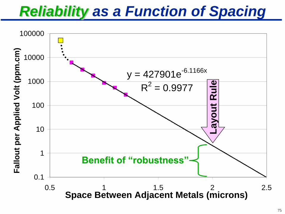
y = 427901e-6.1166x
R2 = 0.9977
0.1
1
10
100
1000
10000
100000
0.5 1 1.5 2 2.5Space Between Adjacent Metals (microns)
Fallo
ut
per
Ap
plied
Vo
lt (
pp
m.c
m)
Layo
ut
Ru
le
Benefit of “robustness”
Reliability as a Function of Spacing

76
Voltage Aging Effects – Narrow Gap Defect Distribution Vs. Voltage with
3600 second, 2V lifetest inserted
Voltage and time relationships are similar between
capacitors and amplified interconnect.
1 h
r L
ifete
st
0.1
0.2
0.3
0.4
0.5
0.6
1 2 3 4 5 6 7 8 9 10
Voltage (Volts)
Qu
ali
ty L
evel
(%
)
Defect Distribution (with interruption)
2V Lifetest Fallout (12s, 15s, 39s, 50s, 3460s)
Reference Distribution (w/o interruption)
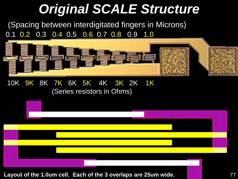
Layout of the 1.0um cell. Each of the 3 overlaps are 25um wide.
Original SCALE Structure
Desire a compact PCM-style
structure to measure liftoff
quality at a single voltage
10K 9K 8K 7K 6K 5K 4K 3K 2K 1K
(Series resistors in Ohms)
(Spacing between interdigitated fingers in Microns)
0.1 0.2 0.3 0.4 0.5 0.6 0.7 0.8 0.9 1.0
77
78
Scale Sensitivity Over Time (Single V Measurement)
A116505A
A118104A
A119302A
A221401A
A224904A
A228006A
A233702A
A234105A
A301104A
A304003A
A306717A
A313803A
A321505A
A329106A
Run Number
600
800
1000
1200
1400
1600
1800
2000
2200
2400
2600
2800
3000
3200
3400
GA
P_M
0(1316)
L EG END
G AP_ M 0 ( 1 3 1 6 )
M e ta l0 Ba s e line : M e ta l0 Lift-Off Struc ture
2001 2002 2003
78
724 Ω=0.8μ
10.KΩ=0.1μ
4.8KΩ=0.2μ
3.0KΩ=0.3μ
2.1KΩ=0.4μ
1.6KΩ=0.5μ
1.2KΩ=0.6μ
936 Ω=0.7μ
547 Ω=0.9μ
385 Ω=1.0μ
2,671 Reliability Wafers Evaluated

79 79
Applicability of Amplification
●Sampled meter-sized periphery to estimate for centimeters and below.
●Verified layout rules and applicability of periphery amplification.
●Found lower limits of gap amplification, not upper limits. (need more periphery)
●Relationships between Yield & Reliability were demonstrated.
79
80
Outline
Basics
• A little about Compound Semiconductors
• Vocabulary
• A new era for reliability
• Arrhenius methodology review
Beyond the Basics . . . What’s manufacturability got to do with it?
• Learning from customers: it’s a Natural
• Breaking the cycle of learning curves
• Tipping your cap
• The Black magic of current density
• Amped up on defects
• The new PC

81
Finding the “right” stress
• Acceleration Factors known for
Temperature, Voltage, Current.
• Experience from the field does not
match wearout mechanisms.
• Causes of reliability test and field
failures indicate “excursions.”
• Samples: special lot available.

82
Thermal Excursions - Background
• “Special” Lot
• 13,000 samples per wafer
• 14 wafer lot (5 anomalous)
• 200 additional lots screened
(representing 2.6 million)
• >130,500 tested for one mechanism

83
Excursions: Methods - Tests
Test Type JEDEC Range Cycles
1 Infrared Reflow JESD22-A113-B +25ºC to +240ºC <20
2 Thermal Shock JESD22-A106-A Condition D -65ºC to +150ºC <20
3 Thermal Shock JESD26A Condition C-1 -40ºC to +125ºC <100
4 Temperature Cycle JESD22-A104-A Condition G -40ºC to +125ºC <500
5 Thermal Shock JESD22-A106-A Condition B 0ºC to +100ºC <2500
Maximum Minimum Maximum
Test Type Transfer Dwell Time Time to
Time Time Temperature
1 Infrared Reflow ~140 seconds 20 seconds 6 minutes
2 Thermal Shock 10 seconds 2 minutes 5 minutes
3 Thermal Shock 10 seconds 2 minutes 5 minutes
4 Temperature Cycle 1 minute 10 minutes 15 minutes
5 Thermal Shock 10 seconds 2 minutes 5 minutes
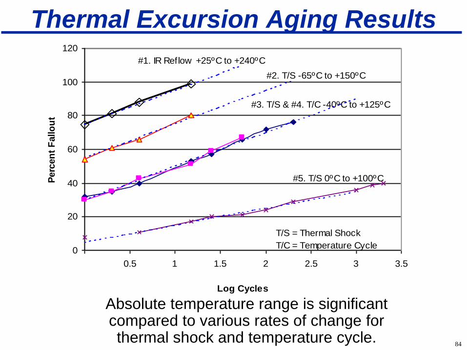
84
0
20
40
60
80
100
120
0 0.5 1 1.5 2 2.5 3 3.5
Log Cycles
Perc
en
t F
allo
ut
#2. T/S -65ºC to +150ºC
#3. T/S & #4. T/C -40ºC to +125ºC
#1. IR Reflow +25ºC to +240ºC
#5. T/S 0ºC to +100ºC
T/S = Thermal Shock
T/C = Temperature Cycle
Thermal Excursion Aging Results
Absolute temperature range is significant compared to various rates of change for thermal shock and temperature cycle.

85
Thermal Excursions: Acceleration
1 Solder Reflow =
8 Thermal Shocks
-65ºC to +150ºC
or
144 Cycles
-40ºC to +125ºC
or
4.99 Million Cycles
0ºC to +100ºC
86
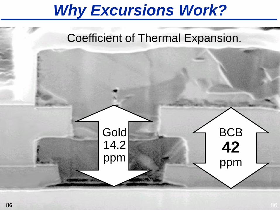
Why Excursions Work?
Coefficient of Thermal Expansion.
Gold 14.2 ppm
BCB
42 ppm
86 86

87
Excursions: Building on the Tool
Structures
Rel Mask Sets PCMs
Products PDQs
Stresses
Bake
Autoclave
Temp. Cycle
IR Reflow
HAST
Power Cycle Constraints
Faster
Time to Fail
Idea!

88
Investigation: Via Chains & Power Cycling
Four Via Chain
Arrays. Up to
6,500 links each.
Each Array
Surrounded by
NiCr “heater”
Resistors.
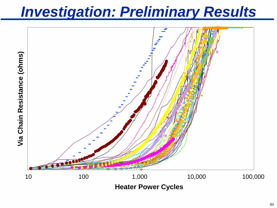
89
Investigation: Preliminary Results
10 100 1,000 10,000 100,000
Heater Power Cycles
Via
Ch
ain
Resis
tan
ce (
oh
ms)

90
Ramp Cycle to Failure Plot (“TDDB” for power cycling)
Ord
ere
d V
ia C
ha
in F
ailu
res
10 100 1,000 10,000
Power Cycles to Failure
91
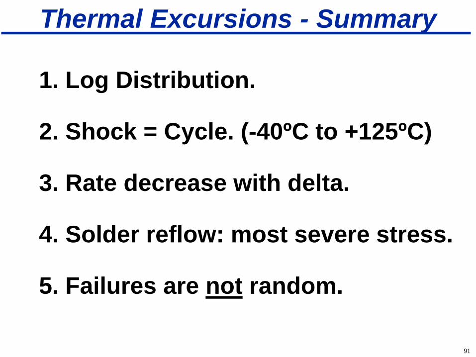
Thermal Excursions - Summary
1. Log Distribution.
2. Shock = Cycle. (-40ºC to +125ºC)
3. Rate decrease with delta.
4. Solder reflow: most severe stress.
5. Failures are not random.
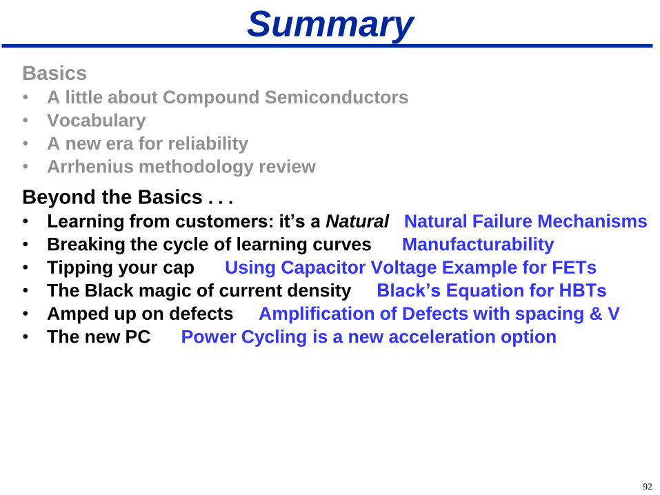
92
Summary
Basics
• A little about Compound Semiconductors
• Vocabulary
• A new era for reliability
• Arrhenius methodology review
Beyond the Basics . . .
• Learning from customers: it’s a Natural Natural Failure Mechanisms
• Breaking the cycle of learning curves Manufacturability
• Tipping your cap Using Capacitor Voltage Example for FETs
• The Black magic of current density Black’s Equation for HBTs
• Amped up on defects Amplification of Defects with spacing & V
• The new PC Power Cycling is a new acceleration option
93
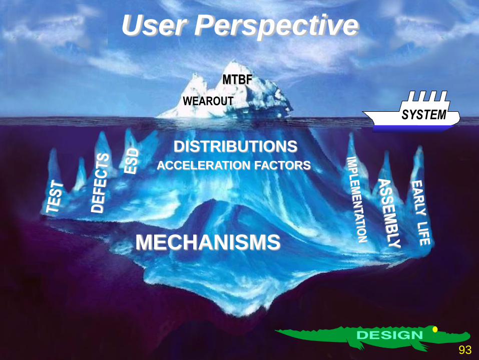
User Perspective
WEAROUT
MTBF
DISTRIBUTIONS ACCELERATION FACTORS
MECHANISMS
SYSTEM
93
94
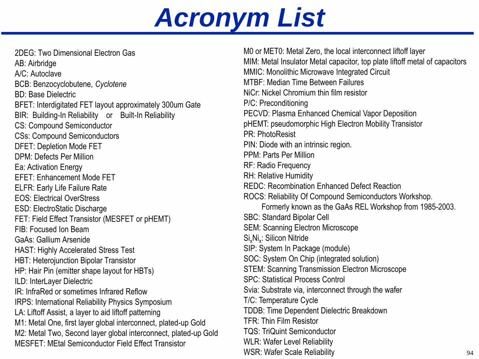
Acronym List 2DEG: Two Dimensional Electron Gas
AB: Airbridge
A/C: Autoclave
BCB: Benzocyclobutene, Cyclotene
BD: Base Dielectric
BFET: Interdigitated FET layout approximately 300um Gate
BIR: Building-In Reliability or Built-In Reliability
CS: Compound Semiconductor
CSs: Compound Semiconductors
DFET: Depletion Mode FET
DPM: Defects Per Million
Ea: Activation Energy
EFET: Enhancement Mode FET
ELFR: Early Life Failure Rate
EOS: Electrical OverStress
ESD: ElectroStatic Discharge
FET: Field Effect Transistor (MESFET or pHEMT)
FIB: Focused Ion Beam
GaAs: Gallium Arsenide
HAST: Highly Accelerated Stress Test
HBT: Heterojunction Bipolar Transistor
HP: Hair Pin (emitter shape layout for HBTs)
ILD: InterLayer Dielectric
IR: InfraRed or sometimes Infrared Reflow
IRPS: International Reliability Physics Symposium
LA: Liftoff Assist, a layer to aid liftoff patterning
M1: Metal One, first layer global interconnect, plated-up Gold
M2: Metal Two, Second layer global interconnect, plated-up Gold
MESFET: MEtal Semiconductor Field Effect Transistor
M0 or MET0: Metal Zero, the local interconnect liftoff layer
MIM: Metal Insulator Metal capacitor, top plate liftoff metal of capacitors
MMIC: Monolithic Microwave Integrated Circuit
MTBF: Median Time Between Failures
NiCr: Nickel Chromium thin film resistor
P/C: Preconditioning
PECVD: Plasma Enhanced Chemical Vapor Deposition
pHEMT: pseudomorphic High Electron Mobility Transistor
PR: PhotoResist
PIN: Diode with an intrinsic region.
PPM: Parts Per Million
RF: Radio Frequency
RH: Relative Humidity
REDC: Recombination Enhanced Defect Reaction
ROCS: Reliability Of Compound Semiconductors Workshop.
Formerly known as the GaAs REL Workshop from 1985-2003.
SBC: Standard Bipolar Cell
SEM: Scanning Electron Microscope
SixNix: Silicon Nitride
SIP: System In Package (module)
SOC: System On Chip (integrated solution)
STEM: Scanning Transmission Electron Microscope
SPC: Statistical Process Control
Svia: Substrate via, interconnect through the wafer
T/C: Temperature Cycle
TDDB: Time Dependent Dielectric Breakdown
TFR: Thin Film Resistor
TQS: TriQuint Semiconductor
WLR: Wafer Level Reliability
WSR: Wafer Scale Reliability
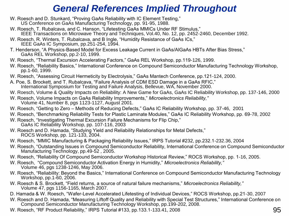
General References Implied Throughout W. Roesch and D. Stunkard, “Proving GaAs Reliability with IC Element Testing,”
US Conference on GaAs Manufacturing Technology, pp. 91-95, 1988.
W. Roesch, T. Rubalcava, and C. Hanson, “Lifetesting GaAs MMICs Under RF Stimulus,” IEEE Transactions on Microwave Theory and Techniques, Vol.40, No. 12, pp. 2452-2460, December 1992.
W. Roesch, R. Winters, T. Rubalcava, and B Ingle, “Humidity Resistance of GaAs ICs,” IEEE GaAs IC Symposium, pp.251-254, 1994.
T. Henderson, “A Physics-Based Model for Excess Leakage Current in GaAs/AlGaAs HBTs After Bias Stress,” GaAs REL Workshop, pp.2-10, 1999.
W. Roesch, “Thermal Excursion Accelerating Factors,” GaAs REL Workshop, pp.119-126, 1999.
W. Roesch, “Reliability Basics,” International Conference on Compound Semiconductor Manufacturing Technology Workshop, pp.1-60, 1999.
W. Roesch, “Assessing Circuit Hermeticity by Electrolysis,” GaAs Mantech Conference, pp.121-124, 2000.
A. Poe, S. Brockett, and T. Rubalcava, “Failure Analysis of CDM ESD Damage in a GaAs RFIC,” International Symposium for Testing and Failure Analysis, Bellevue, WA, November 2000.
W. Roesch, Volume & Quality Impacts on Reliability: A New Game for GaAs, GaAs IC Reliability Workshop, pp. 137-146, 2000
W. Roesch, Volume Impacts on GaAs Reliability Improvements,” Microelectronics Reliability,” Volume 41, Number 8, pgs 1123-1127, August 2001.
W. Roesch, “Getting to Zero – Methods of Reducing Defects,” GaAs IC Reliability Workshop, pp. 37-46, 2001
W. Roesch, “Benchmarking Reliability Tests for Plastic Laminate Modules,” GaAs IC Reliability Workshop, pp. 69-78, 2002
W. Roesch, “Investigating Thermal Excursion Failure Mechanisms for Flip Chip,” GaAs IC Reliability Workshop, pp. 107-116, 2003
W. Roesch and D. Hamada, “Studying Yield and Reliability Relationships for Metal Defects,” ROCS Workshop, pp. 121-133, 2004.
W. Roesch, “MMIC Manufacturing & Packaging Reliability Issues,” IRPS Tutorial #232, pp.232.1-232.36, 2004
W. Roesch, “Outstanding Issues in Compound Semiconductor Reliability, International Conference on Compound Semiconductor Manufacturing Technology, pp.49-52 , 2005.
W. Roesch, “Reliability Of Compound Semiconductor Workshop Historical Review,” ROCS Workshop, pp. 1-16, 2005.
W. Roesch, “Compound Semiconductor Activation Energy in Humidity,” Microelectronics Reliability,” Volume 46, pgs 1238-1246, May 2006.
W. Roesch, “Reliability: Beyond the Basics,” International Conference on Compound Semiconductor Manufacturing Technology Workshop, pp.1-60, 2006.
W. Roesch & S. Brockett, “Field returns, a source of natural failure mechanisms,” Microelectronics Reliability,” Volume 47, pgs 1156-1165, March 2007.
D. Hamada & W. Roesch, “Wafer-Level Accelerated Lifetesting of Individual Devices,” ROCS Workshop, pp.21-30, 2007
W. Roesch and D. Hamada, “Measuring Liftoff Quality and Reliability with Special Test Structures,” International Conference on Compound Semiconductor Manufacturing Technology Workshop, pp.199-202, 2008.
W. Roesch, “RF Product Reliability,” IRPS Tutorial #133, pp.133.1-133.41, 2008 95