Related products DFN8 2x2 mm - STMicroelectronics · Symbol Parameter Condition Min. Typ. Max. Unit...
23
July 2017 DocID026989 Rev 4 1/23 This is information on a product in full production. www.st.com TSX393 Micropower dual CMOS voltage comparators Datasheet - production data Features Low supply current: 5 μA typ. per comparator Wide single supply range 2.7 V to 16 V or dual supplies (±1.35 V to ±8 V) Extremely low input bias current: 1 pA typ. Input common-mode voltage range includes ground Open drain output High input impedance: 10 12 Ω typ Fast response time: 2 μs typ. for 5 mV overdrive ESD tolerance: 4 kV HBM, 200 V MM Related products Pin-to-pin and functionally compatible with the dual CMOS TS393 comparators See the TSX3702 for push-pull output Applications Automotive Industrial Description The TSX393 is a micropower CMOS dual voltage comparator which exhibits a very low current consumption of 5 μA typical per comparator. This device was designed as the improvement of the TS393: it shows a lower current consumption, a better input offset voltage, and an enhanced ESD tolerance. The TSX393 is fully specified over a wide temperature range and is proposed in automotive grade for the SO8 package. It is fully compatible with the TS393 CMOS comparator and is available with similar packages. New tiny packages (MiniSO8 and DFN8 2x2 mm) are also proposed for the TSX393 thus allowing even more integration on applications. S MiniSO8 (plastic package) D SO8 (plastic micropackage) P TSSOP8 (thin shrink small outline package) DFN8 2x2 mm (plastic micropackage)
Transcript of Related products DFN8 2x2 mm - STMicroelectronics · Symbol Parameter Condition Min. Typ. Max. Unit...

July 2017 DocID026989 Rev 4 1/23
This is information on a product in full production. www.st.com
TSX393
Micropower dual CMOS voltage comparators
Datasheet - production data
Features Low supply current: 5 µA typ. per
comparator Wide single supply range 2.7 V to 16 V or
dual supplies (±1.35 V to ±8 V) Extremely low input bias current: 1 pA typ.
Input common-mode voltage range includes ground
Open drain output High input impedance: 1012 Ω typ Fast response time: 2 µs typ. for 5 mV
overdrive ESD tolerance: 4 kV HBM, 200 V MM
Related products Pin-to-pin and functionally compatible with
the dual CMOS TS393 comparators See the TSX3702 for push-pull output
Applications Automotive Industrial
Description The TSX393 is a micropower CMOS dual voltage comparator which exhibits a very low current consumption of 5 µA typical per comparator. This device was designed as the improvement of the TS393: it shows a lower current consumption, a better input offset voltage, and an enhanced ESD tolerance. The TSX393 is fully specified over a wide temperature range and is proposed in automotive grade for the SO8 package. It is fully compatible with the TS393 CMOS comparator and is available with similar packages. New tiny packages (MiniSO8 and DFN8 2x2 mm) are also proposed for the TSX393 thus allowing even more integration on applications.
S
MiniSO8
(plastic package)
D
SO8
(plastic micropackage)
P
TSSOP8
(thin shrink small outline package)
DFN8 2x2 mm
(plastic micropackage)

Contents TSX393
2/23 DocID026989 Rev 4
Contents
1 Package pin connections ................................................................ 3
2 Absolute maximum ratings ............................................................. 4
3 Operating conditions ...................................................................... 5
4 Schematic diagram .......................................................................... 6
5 Electrical characteristics ................................................................ 7
6 Application information (input voltages) ..................................... 14
7 Package information ..................................................................... 15
7.1 SO8 package information ................................................................ 16
7.2 TSSOP8 package information ......................................................... 17
7.3 DFN8 2x2 package information ....................................................... 18
7.4 MiniSO8 package information ......................................................... 20
8 Ordering information ..................................................................... 21
9 Revision history ............................................................................ 22
TSX393 Package pin connections
DocID026989 Rev 4 3/23
1 Package pin connections Figure 1: Pin connections top view
Out1
In1-
In1+
Vcc-
Vcc+
Out2
In2-
In2+
1
2
3
4 5
6
7
8
-
+
+
-
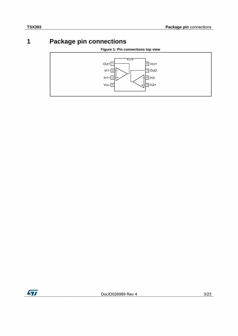
Absolute maximum ratings TSX393
4/23 DocID026989 Rev 4
2 Absolute maximum ratings Table 1: Absolute maximum ratings (AMR)
Symbol Parameter Value Unit
VCC+ Supply voltage(1) 18
V Vid Differential input voltage(2) ±18
Vin Input voltage(3) -0.3 to 18
Vo Output voltage 18
Io Output current 20 mA
IF Forward current in ESD protection diodes on inputs(4) 50
Tj Maximum junction temperature 150 ºC
Rthja Thermal resistance junction to ambient(5)
SO8 125
ºC/W TSSOP8 120
MiniSO8 190
DFN8 2x2 115
Tstg Storage temperature range -65 to 150 ºC
ESD
HBM: human body model(6) 4000
V MM: machine model(7) 200
CDM: charged device model(8) 1500
Latch-up immunity 200 mA
Notes:
(1)All voltage values, except the differential voltage, are with respect to network ground terminal (2)Differential voltages are the non-inverting input terminal with respect to the inverting input terminal (3)Excursions of input voltages may exceed the power supply level. As long as the common mode voltage (Vicm = (Vin+) + (Vin-)/2) remains within the specified range, the comparator provides a stable output state. However, the maximum current of the input stage, through the ESD diodes (IF), must be strictly observed. (4)Guaranteed by design (5)Short-circuits can cause excessive heating and destructive dissipation. Values are typical. (6)According to JEDEC standard JESD22-A114F (7)According to JEDEC standard JESD22-A115A (8)According to ANSI/ESD STM5.3.1

TSX393 Operating conditions
DocID026989 Rev 4 5/23
3 Operating conditions Table 2: Operating conditions
Symbol Parameter Value Unit
VCC+ Supply voltage 2.7 to 16
V Vicm
Common mode input voltage range 0 to (VCC+) - 1.5
Tmin ≤ Tamb ≤ Tmax 0 to (VCC+) - 2
Toper Operating free-air temperature range -40 to 125 ºC

Schematic diagram TSX393
6/23 DocID026989 Rev 4
4 Schematic diagram Figure 2: Schematic diagram (one operator)
ESD
CLAMPIN-IN+ OUT
VCC+
VCC-

TSX393 Electrical characteristics
DocID026989 Rev 4 7/23
5 Electrical characteristics Table 3: VCC+ = 3 V, VCC- = 0 V, Tamb = 25 ºC (unless otherwise specified)
Symbol Parameter Condition Min. Typ. Max. Unit
Vio Input offset voltage(1) Vicm = 0 V -5 0.1 5
mV Tmin ≤ Tamb ≤ Tmax -6 6
Iio Input offset current(2) Vicm = VCC/2 1 10
pA Tmin ≤ Tamb ≤ Tmax 600
Iib Input bias current (2) Vicm = VCC/2 1 10
Tmin ≤ Tamb ≤ Tmax 1200
CMR Common-mode rejection ratio
Vicm = 0 to (VCC+) - 1.5 V 58 73
dB Vicm = 0 to (VCC+) - 2 V, Tmin ≤ Tamb ≤ Tmax 55
SVR Supply voltage rejection ratio
VCC+ = 3 V to 5 V, Vicm = VCC/2 69 88 Tmin ≤ Tamb ≤ Tmax 69
IOH High-level output voltage
Vid = 1 V, VOH = 3 V 1 40 nA
Tmin ≤ Tamb ≤ Tmax 1000
VOL Low-level output voltage
Vid = -1 V, IOL = 4 mA 300 400 mV
Tmin ≤ Tamb ≤ Tmax 600
ICC Supply current per comparator
No load, outputs low 5 6
μA Tmin ≤ Tamb ≤ Tmax 7
No load, outputs high 8 9
Tmin ≤ Tamb ≤ Tmax 11
tPLH Response time low to high
Vicm = 0 V, f = 10 kHz, RL = 5.1 kΩ, CL = 50 pF, overdrive = 5 mV 2.5
μs
Overdrive = 100 mV 0.53 0.65
Tmin ≤ Tamb ≤ Tmax 0.7
tPHL Response time high to low
Vicm = 0 V, f = 10 kHz, RL = 5.1 kΩ, CL = 50 pF, overdrive = 5 mV 2.0 Overdrive = 100 mV 0.4 0.6
Tmin ≤ Tamb ≤ Tmax 0.65
tf Fall time f = 10 kHz, CL = 50 pF, RL = 5.1 kΩ, overdrive 50 mV 39 ns
Notes:
(1)The specified offset voltage is the maximum value required to drive the output up to 2.5 V or down to 0.3 V (2)Guaranteed by design

Electrical characteristics TSX393
8/23 DocID026989 Rev 4
Table 4: VCC+ = 5 V, VCC- = 0 V, Tamb = 25 ºC (unless otherwise specified)
Symbol Parameter Condition Min. Typ. Max. Unit
Vio Input offset voltage(1) Vicm = VCC/2 -5 0.1 5
mV Tmin ≤ Tamb ≤ Tmax -6 6
Iio Input offset current(2) Vicm = VCC/2 1 10
pA Tmin ≤ Tamb ≤ Tmax 600
Iib Input bias current (2) Vicm = VCC/2 1 10
Tmin ≤ Tamb ≤ Tmax 1200
CMR Common-mode rejection ratio
Vicm = 0 to (VCC+) - 1.5 V 66 85
dB Vicm = 0 to (VCC+) - 2 V, Tmin ≤ Tamb ≤ Tmax 65
SVR Supply voltage rejection ratio
VCC+ = 5 V to 10 V, Vicm = VCC/2 71 89 Tmin ≤ Tamb ≤ Tmax 70
IOH High-level output voltage
Vid = 1 V, VOH = 5 V 1 40 nA
Tmin ≤ Tamb ≤ Tmax 1000
VOL Low-level output voltage
Vid = -1 V, IOL = 4 mA 180 250 mV
Tmin ≤ Tamb ≤ Tmax 400
ICC Supply current per comparator
No load, outputs low 5 8
μA Tmin ≤ Tamb ≤ Tmax 9
No load, outputs high 9 10
Tmin ≤ Tamb ≤ Tmax 11
tPLH Response time low to high
Vicm = 0 V, f = 10 kHz, RL = 5.1 kΩ, CL = 50 pF, overdrive = 5 mV 2.5
μs
Overdrive = 10 mV 1.6 Overdrive = 20 mV 1.0 Overdrive = 40 mV 0.7 Overdrive = 100 mV 0.52 0.6
Tmin ≤ Tamb ≤ Tmax 0.7
TTL input(3) 0.55 0.7
Tmin ≤ Tamb ≤ Tmax 0.75
tPHL Response time high to low
Vicm = 0 V, f = 10 kHz, RL = 5.1 kΩ, CL = 50 pF, overdrive = 5 mV 2.8 Overdrive = 10 mV 1.8 Overdrive = 20 mV 1.0 Overdrive = 40 mV 0.7 Overdrive = 100 mV 0.46 0.6
Tmin ≤ Tamb ≤ Tmax 0.7
TTL input (3) 0.30 0.40
Tmin ≤ Tamb ≤ Tmax 0.50

TSX393 Electrical characteristics
DocID026989 Rev 4 9/23
Symbol Parameter Condition Min. Typ. Max. Unit
tf Fall time f = 10 kHz, CL = 50 pF, RL = 5.1 kΩ, overdrive 50 mV 30 ns
Notes:
(1)The specified offset voltage is the maximum value required to drive the output up to 4.5 V or down to 0.3 V (2)Guaranteed by design (3)A step from 0 V to 3 V is applied on one input while the other is fixed at 1.4 V. Response time is the time interval between the application of the input voltage step and the moment the output voltage reaches 50 % of its final value.
Table 5: VCC+ = 16 V, VCC- = 0 V, Tamb = 25 ºC (unless otherwise specified)
Symbol Parameter Condition Min. Typ. Max. Unit
Vio Input offset voltage(1) Vicm = VCC/2 -5 0.1 5
mV Tmin ≤ Tamb ≤ Tmax -6 6
Iio Input offset current(2) Vicm = VCC/2 1 10
pA Tmin ≤ Tamb ≤ Tmax 600
Iib Input bias current(2) Vicm = VCC/2 1 10
Tmin ≤ Tamb ≤ Tmax 1200
CMR Common-mode rejection ratio
Vicm = 0 to (VCC+) - 1.5 V 72 90
dB Vicm = 0 to (VCC+) - 2 V, Tmin ≤ Tamb ≤ Tmax 70
SVR Supply voltage rejection ratio
VCC+ = 5 V to 16 V, Vicm = VCC/2 73 90 Tmin ≤ Tamb ≤ Tmax 72
IOH High-level output voltage
Vid = 1 V, VOH = 16 V 1 40 nA
Tmin ≤ Tamb ≤ Tmax 1000
VOL Low-level output voltage
Vid = -1 V, IOL = 4 mA 90 150 mV
Tmin ≤ Tamb ≤ Tmax 250
ICC Supply current per comparator
No load, outputs low 7 9
μA Tmin ≤ Tamb ≤ Tmax 10
No load, outputs high 11 13
Tmin ≤ Tamb ≤ Tmax 14
tPLH Response time low to high
Vicm = 0 V, f = 10 kHz, RL = 5.1 kΩ, CL = 50 pF, overdrive = 5 mV 2.3
μs
Overdrive = 10 mV 1.5 Overdrive = 20 mV 1.0 Overdrive = 40 mV 0.7 Overdrive = 100 mV 0.55 0.65
Tmin ≤ Tamb ≤ Tmax 0.70
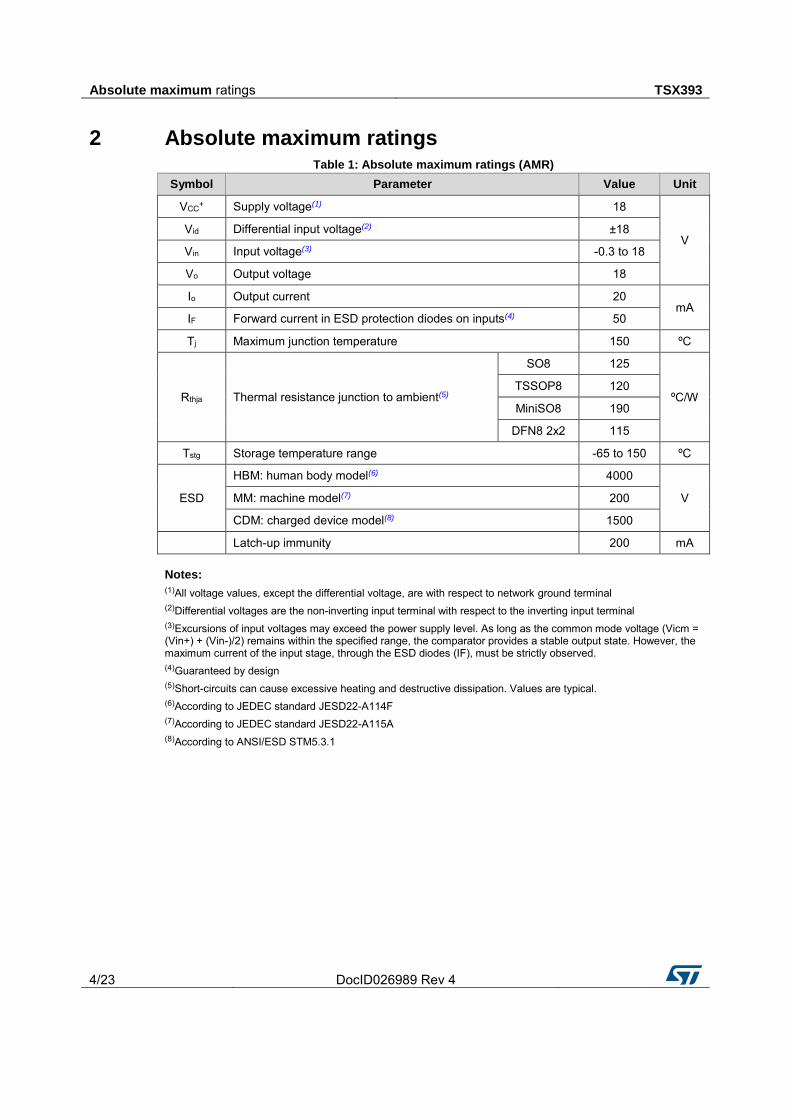
tPHL Response time high to low
Vicm = 0 V, f = 10 kHz, RL = 5.1 kΩ, CL = 50 pF, overdrive = 5 mV 2.4 Overdrive = 10 mV 1.6
Electrical characteristics TSX393
10/23 DocID026989 Rev 4
Symbol Parameter Condition Min. Typ. Max. Unit
Overdrive = 20 mV 1.0 Overdrive = 40 mV 0.7 Overdrive = 100 mV 0.55 0.70
Tmin ≤ Tamb ≤ Tmax 0.75
tf Fall time f = 10 kHz, CL = 50 pF, RL = 5.1 kΩ, overdrive 50 mV 11 ns
Notes:
(1)The specified offset voltage is the maximum value required to drive the output up to 4.5 V or down to 0.3 V (2)Guaranteed by design

TSX393 Electrical characteristics
DocID026989 Rev 4 11/23
Figure 3: Current consumption vs. supply voltage, output high
Figure 4: Current consumption vs. supply voltage, output low
Figure 5: Current consumption vs. input
common-mode voltage, output high
Figure 6: Current consumption vs. common-mode voltage, output low
Figure 7: Output leakage current vs. output
voltage, VCC = 5 V
Figure 8: Output leakage current vs. supply voltage, VCC = 5 V

Electrical characteristics TSX393
12/23 DocID026989 Rev 4
0 2 4 6 8 10 12 14 161E-141E-131E-121E-111E-101E-91E-81E-71E-61E-51E-41E-3
VCC= 5VT = 85oC
T = 25oC
T = 125oC
I ib(A
)
Vin (V)
Figure 9: Output voltage drop vs. output sink current, VCC = 5 V
Figure 10: Output voltage drop vs. output sink current, VCC = 12 V
Figure 11: Input offset voltage distribution, VCC = 5 V
Figure 12: Input current vs input voltage, VCC = 5 V
Figure 13: Propagation delay tPLH vs. input signal overdrive, VCC = 5 V
Figure 14: Propagation delay tPHL vs. input signal overdrive, VCC = 5 V
TSX393 Electrical characteristics
DocID026989 Rev 4 13/23
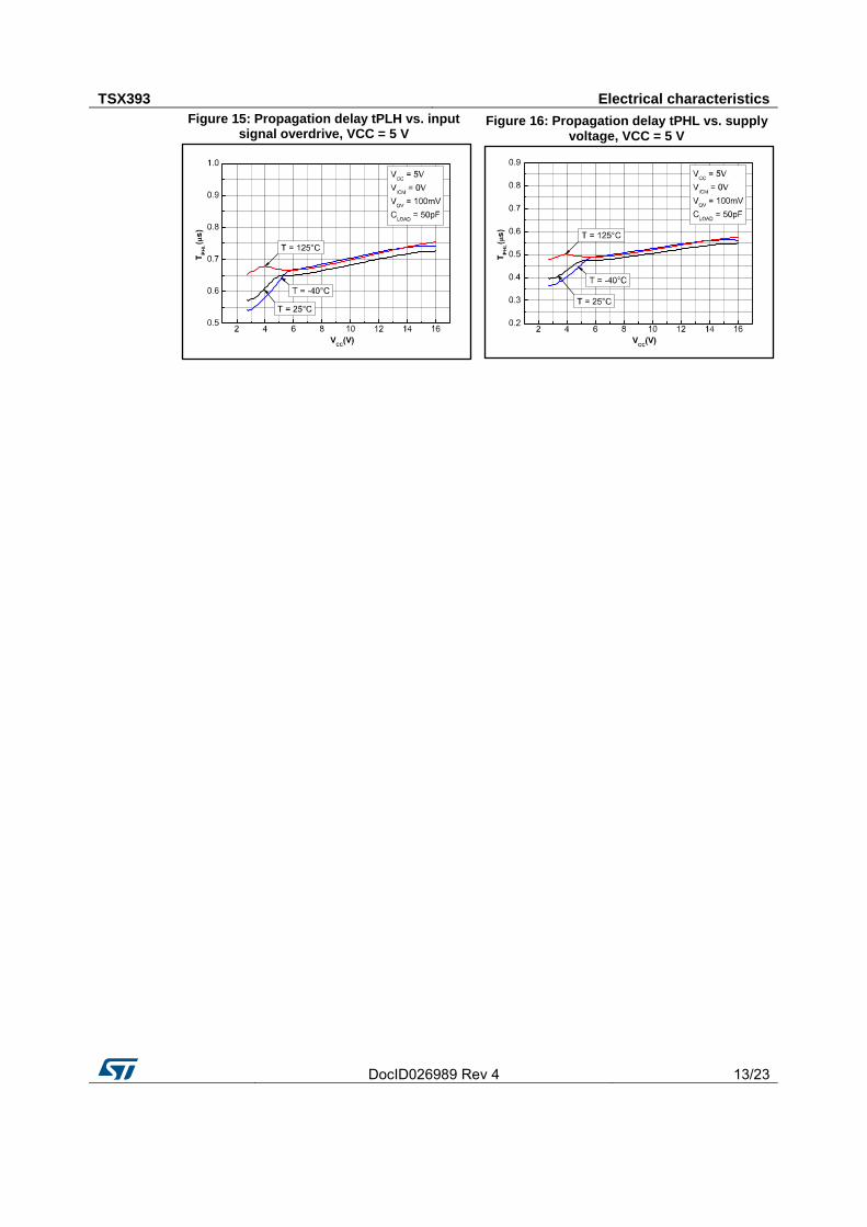
Figure 15: Propagation delay tPLH vs. input signal overdrive, VCC = 5 V
Figure 16: Propagation delay tPHL vs. supply voltage, VCC = 5 V

Application information (input voltages) TSX393
14/23 DocID026989 Rev 4
6 Application information (input voltages)
The ESD strategy used in the TSX393 (and shown in Figure 2 allows input voltages from -0.3 V up to 16 V to be applied regardless of the VCC+ voltage. When VIN > VCC+ a leakage current goes from the input through the protection diode to the ESD clamp. This current is about 0.2 nA at 25 °C and about 250 nA at 125 °C. For a detailed input characteristic see Figure 12. The device is designed to prevent phase reversal.
TSX393 Package information
DocID026989 Rev 4 15/23
7 Package information
In order to meet environmental requirements, ST offers these devices in different grades of ECOPACK® packages, depending on their level of environmental compliance. ECOPACK® specifications, grade definitions and product status are available at: www.st.com. ECOPACK® is an ST trademark.

Package information TSX393
16/23 DocID026989 Rev 4
7.1 SO8 package information
Figure 17: SO8 package outline
Table 6: SO8 mechanical data
Ref.
Dimensions
Millimeters Inches
Min. Typ. Max. Min. Typ. Max
A
1.75
0.069
A1 0.10
0.25 0.004
0.010
A2 1.25
0.049
b 0.28
0.48 0.011
0.019
c 0.17
0.23 0.007
0.010
D 4.80 4.90 5.00 0.189 0.193 0.197
E 5.80 6.00 6.20 0.228 0.236 0.244
E1 3.80 3.90 4.00 0.150 0.154 0.157
e
1.27
0.050
h 0.25
0.50 0.010
0.020
L 0.40
1.27 0.016
0.050
L1
1.04
0.040
k 0°
8° 0°
8°
ccc
0.10
0.004

TSX393 Package information
DocID026989 Rev 4 17/23
7.2 TSSOP8 package information
Figure 18: TSSOP8 package outline
Table 7: TSSOP8 mechanical data
Ref.
Dimensions
Millimeters Inches
Min. Typ. Max. Min. Typ. Max.
A
1.2
0.047
A1 0.05
0.15 0.002
0.006
A2 0.80 1.00 1.05 0.031 0.039 0.041
b 0.19
0.30 0.007
0.012
c 0.09
0.20 0.004
0.008
D 2.90 3.00 3.10 0.114 0.118 0.122
E 6.20 6.40 6.60 0.244 0.252 0.260
E1 4.30 4.40 4.50 0.169 0.173 0.177
e
0.65
0.0256
k 0°
8° 0°
8°
L 0.45 0.60 0.75 0.018 0.024 0.030
L1
1
0.039
aaa
0.1
0.004

Package information TSX393
18/23 DocID026989 Rev 4
7.3 DFN8 2x2 package information
Figure 19: DFN8 2x2 package outline
Table 8: DFN8 2x2 mechanical data
Ref.
Dimensions
Millimeters Inches
Min. Typ. Max. Min. Typ. Max.
A 0.70 0.75 0.80 0.028 0.030 0.031
A1 0.00 0.02 0.05 0.000 0.001 0.002
b 0.15 0.20 0.25 0.006 0.008 0.010
D
2.00
0.079
E
2.00
0.079
e
0.50
0.020
L 0.045 0.55 0.65 0.018 0.022 0.026
N 8
TSX393 Package information
DocID026989 Rev 4 19/23
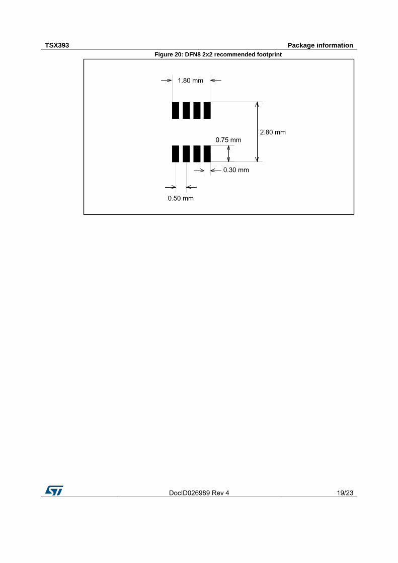
Figure 20: DFN8 2x2 recommended footprint
1.80 mm
2.80 mm0.75 mm
0.30 mm
0.50 mm

Package information TSX393
20/23 DocID026989 Rev 4
7.4 MiniSO8 package information
Figure 21: MiniSO8 package outline
Table 9: MiniSO8 mechanical data
Ref.
Dimensions
Millimeters Inches
Min. Typ. Max. Min. Typ. Max.
A
1.1
0.043
A1 0
0.15 0
0.006
A2 0.75 0.85 0.95 0.030 0.033 0.037
b 0.22
0.40 0.009
0.016
c 0.08
0.23 0.003
0.009
D 2.80 3.00 3.20 0.11 0.118 0.126
E 4.65 4.90 5.15 0.183 0.193 0.203
E1 2.80 3.00 3.10 0.11 0.118 0.122
e
0.65
0.026
L 0.40 0.60 0.80 0.016 0.024 0.031
L1
0.95
0.037
L2
0.25
0.010
k 0°
8° 0°
8°
ccc
0.10
0.004
TSX393 Ordering information
DocID026989 Rev 4 21/23
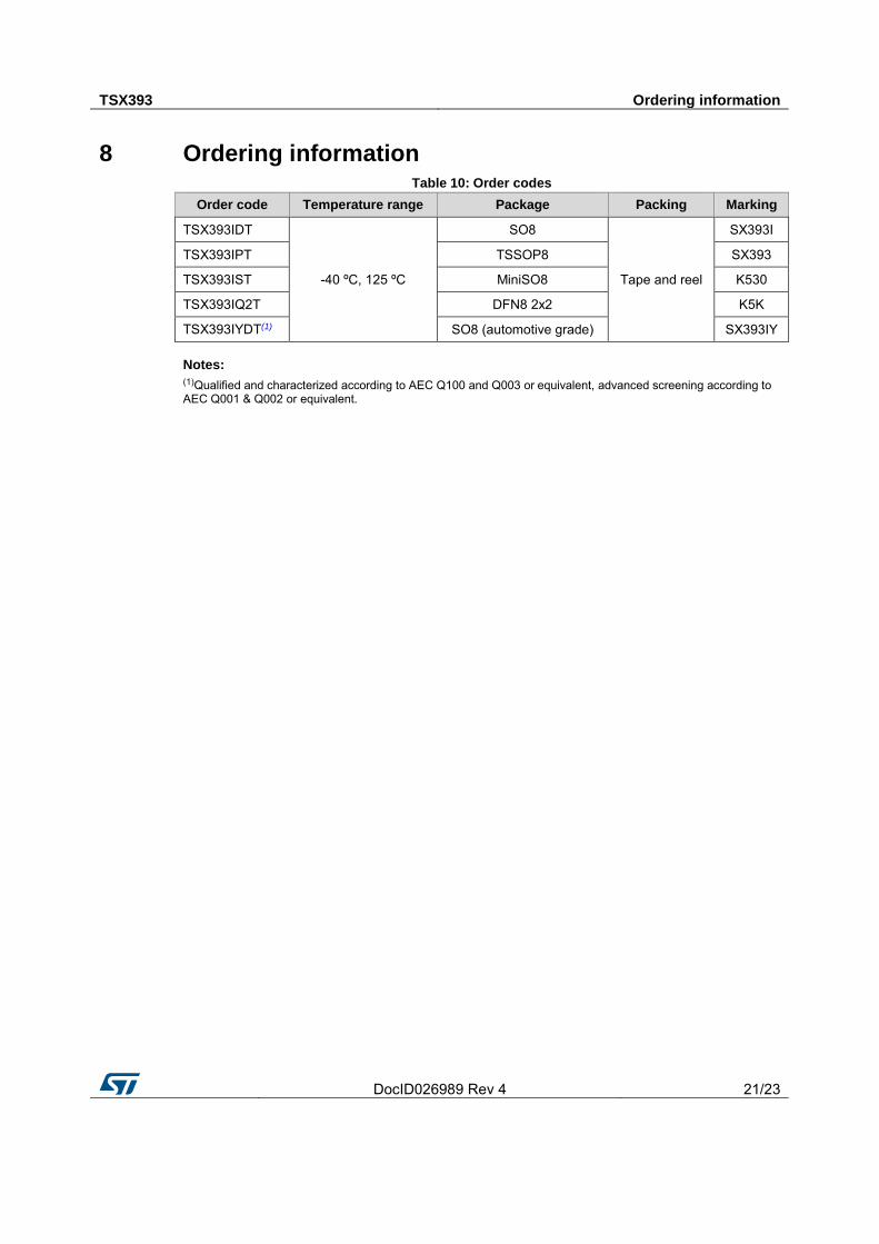
8 Ordering information Table 10: Order codes
Order code Temperature range Package Packing Marking
TSX393IDT
-40 ºC, 125 ºC
SO8
Tape and reel
SX393I
TSX393IPT TSSOP8 SX393
TSX393IST MiniSO8 K530
TSX393IQ2T DFN8 2x2 K5K
TSX393IYDT(1) SO8 (automotive grade) SX393IY
Notes:
(1)Qualified and characterized according to AEC Q100 and Q003 or equivalent, advanced screening according to AEC Q001 & Q002 or equivalent.

Revision history TSX393
22/23 DocID026989 Rev 4
9 Revision history Table 11: Document revision history
Date Revision Changes
30-Oct-2014 1 Initial release.
07-Sep-2015 2
Table 1: "Absoluet maximum ratings (AMR)": updated Rthja value for the DFN8 2x2 package. Section 7.3" "DFN8 2x2 package information": replaced pacakge outline, mechanical data, and recommended footprint by "non-exposed" pad information.
06-Jun-2016 3
Table 3, Table 4, and Table 5: updated Iio and Iib temperature max values, updated VOL condition. In Table 3 only, updated tPHL max value. In Table 5 only, updated IOH condition. Table 10: updated automotive footnote.
06-Jul-2017 4 Table 10: updated automotive footnote.

TSX393
DocID026989 Rev 4 23/23
IMPORTANT NOTICE – PLEASE READ CAREFULLY
STMicroelectronics NV and its subsidiaries (“ST”) reserve the right to make changes, corrections, enhancements, modifications , and improvements to ST products and/or to this document at any time without notice. Purchasers should obtain the latest relevant information on ST products before placing orders. ST products are sold pursuant to ST’s terms and conditions of sale in place at the time of order acknowledgement.
Purchasers are solely responsible for the choice, selection, and use of ST products and ST assumes no liability for application assistance or the design of Purchasers’ products.
No license, express or implied, to any intellectual property right is granted by ST herein.
Resale of ST products with provisions different from the information set forth herein shall void any warranty granted by ST for such product.
ST and the ST logo are trademarks of ST. All other product or service names are the property of their respective owners.
Information in this document supersedes and replaces information previously supplied in any prior versions of this document.
© 2017 STMicroelectronics – All rights reserved
![Dimensions: [mm] Recommended Hole Pattern: [mm] Electrical ... · R 630 V (DC) Insulation Resistance 1 min @ 500 V (DC) R ISO 30000 MΩ min. Dissipation Factor @ 1 kHz DF 0.1 % max.](https://static.fdocuments.in/doc/165x107/604ef7bad686fb6c7b6202eb/dimensions-mm-recommended-hole-pattern-mm-electrical-r-630-v-dc-insulation.jpg)