Regularity for Reduced Variability - Columbia University · 28 July 2006 Regularity for Reduced...
34
28 July 2006 www.c2s2.org Regularity for Reduced Variability Regularity for Reduced Variability Larry Pileggi Carnegie Mellon [email protected]
Transcript of Regularity for Reduced Variability - Columbia University · 28 July 2006 Regularity for Reduced...

28 July 2006
www.c2s2.org
Regularity for Reduced VariabilityRegularity for Reduced VariabilityLarry Pileggi
Carnegie [email protected]

28 July 2006 Slide 2
www.c2s2.org
CMU CollaboratorsCMU CollaboratorsAndrzej StrojwasSlava RovnerTejas JhaveriThiago HersanKim Yaw TongSandeep GuptaXin LiNorris LuiJon ProeselUmut Arslan

28 July 2006 Slide 3
www.c2s2.org
Layout Dependent VariationsLayout Dependent VariationsLayout dependent variations are having an increasingly dominant impact on functional and parametric yield
0%10%20%30%40%50%60%70%80%90%
100%
130nm 90nm 65nm
Pattern Dependent Random Parametric
Per
cent
of Y
ield
Los
s
Source: PDF Solutions

28 July 2006 Slide 4
www.c2s2.org
Layout DependenciesLayout DependenciesExample: Without SRAM-layout specific SPICE models, design closure would be improbable for scaled CMOS
Statistical transistor models based on “all possible”patterns produce a very wide noise margin distribution
SRAM
0.8 0.9 1 1.1 1.20
50
100
150
200
250
Static Noise M argin (Normalized)N
umbe
r of S
ampl
es
DR compliant SPICE models
σ = 0.060
90nm bulk CMOS
28 July 2006 Slide 5
www.c2s2.org
Layout DependenciesLayout Dependencies
SRAM
0.8 0.9 1 1.1 1.20
50
100
150
200
250
Static Noise M argin (Normalized)
Num
ber o
f Sam
ples
SRAM-layout-specific SPICE models
0.8 0.9 1 1.1 1.20
50
100
150
200
250
Static Noise M argin (Normalized)
Num
ber o
f Sam
ples
DR compliant SPICE models
σ = 0.060 σ = 0.026
Based on 1000-simulation-run Monte Carlo

28 July 2006 Slide 6
www.c2s2.org
Micro-RegularityMicro-RegularityGrid of CD shapes with 500nm pitch Frequency response suggests that simple RETs would be effective for controlling this set of patterns
2-D FFT plotsof poly-Si patterns
Highest peak at 2 “Hz”(2 objects per micron)

28 July 2006 Slide 7
www.c2s2.org
Macro-RegularityMacro-RegularityLess restriction is required for the patterns that can be encapsulated within macro-regular pattern groups Can pre-qualify fundamental elements in silicon for known pattern neighborhoods
Pattern neighborhood is known, therefore cells can be reliably implemented to create manufacturable arrays
Macro-Regularity for cell-to-cell variationsMicro-regularity for transistor-to-transistor variations

28 July 2006 Slide 8
www.c2s2.org
90nm Memory Array90nm Memory ArrayMacro-regularity evident from repeated bit-cells
Spread of impulses due to lack of micro-regularity in bit-cells, but patterns validated in silicon via trial-and-error
2-D FFT plotsof poly-Si patterns

28 July 2006 Slide 9
www.c2s2.org
Standard Logic CellsStandard Logic CellsIncreasingly difficult to apply RETs and precisely print all patterns with a single optical setup for these 90nm std cells
2-D FFT plotsof poly-Si patterns

28 July 2006 Slide 10
www.c2s2.org
Micro- and Macro-Variability ImpactMicro- and Macro-Variability ImpactEx: identical min size transistors measured for three different physical environments on the same 65nm IC
Macro-regularity can provide for identical pattern environments for devices and “cells”
Micro-regularity is an area/performance vs. variability trade-off
Source: PDF Solutions
-10.50-10.00-9.50-9.00-8.50-8.00
-7.00
-6.00
300.00 400.00 500.00 600.00 700.00 800.00Idrive
Ioff
(log)
Env I Env II Env III

28 July 2006 Slide 11
www.c2s2.org
Full Adder Ring OscillatorFull Adder Ring Oscillator
1 0
CinCoutB_7 A_7
sum … 0
osc1 0
CinCoutB_6 A_6
sum
1 0
CinCoutB_1 A_1
sum
1 0
CinCoutB_0 A_0
sum
Micro-regular layout expected to enhance printabilityExpect reduced variability – tighter Tp and Idc variation
E.g. Tp ~ gate_length; Idc ~ exp(gate_length)

28 July 2006 Slide 12
www.c2s2.org
Layout ComparisonLayout Comparison
Regular Logic Fabrics2.88μm x 3.2 μm ≈ 9.2 μm2
Standard cell mirror adder3.6μm x 2.6 μm ≈ 9.4 μm2
Std cell and regular mirror adders Regular adder based on SRAM FEOL-like “pushed rules” that are enabled by regularity to provide for comparable area design
Std cell layout based on wrong-way poly with multiple jogs,
diffusion routing, and multiple metal routing directions
28 July 2006 Slide 13
www.c2s2.org
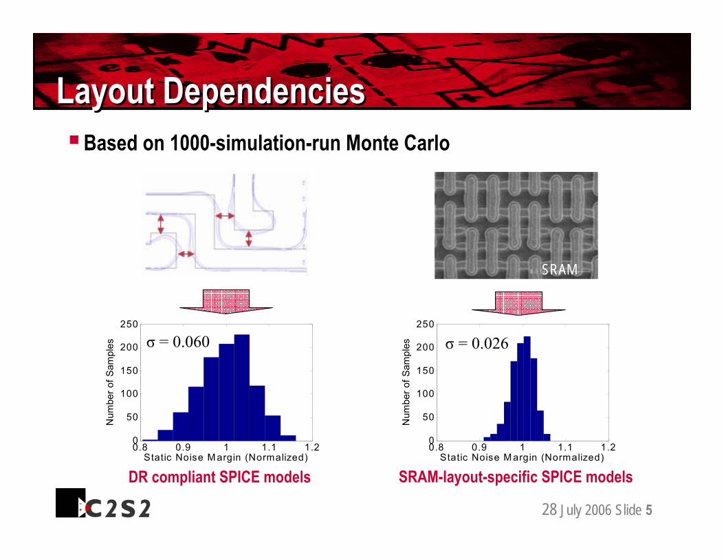
Extra Capacitance on CICO PathExtra Capacitance on CICO Path
Regular Logic FabricsTotal diffusion area at switching nodes =
0.57 μm2
Standard cell mirror adderTotal diffusion area at switching nodes =
0.26 μm2
Larger diffusion areas due to on-grid placement of poly, contacts and metals – but identical transistor sizing for both adders
output
output
internal
input
input
internal
28 July 2006 Slide 14
www.c2s2.org
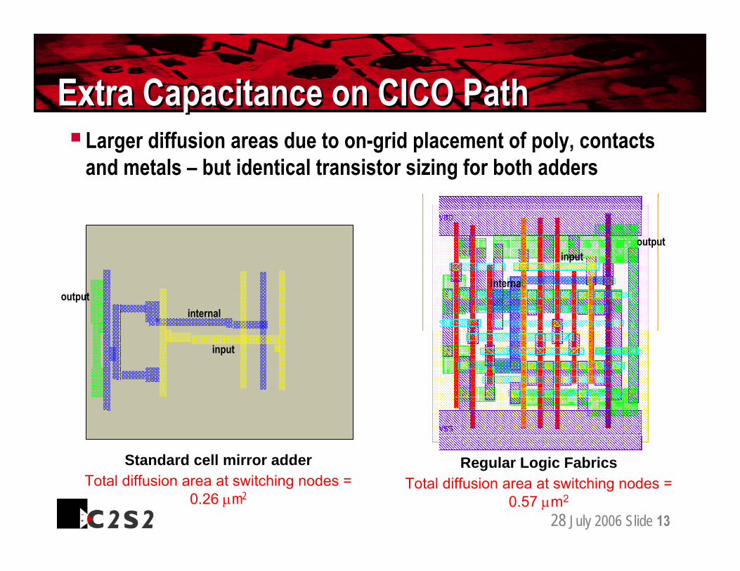
Wafer Probe MeasurementsWafer Probe MeasurementsCommercial 65nm bulk processDistributed ROsthroughout waferMeasured 1 waferthus far (147 sites)2 sites with failedmeasurements for standard cell adderMore measurementsplanned to show consistencyof results across multiple wafers
28 July 2006 Slide 15
www.c2s2.org
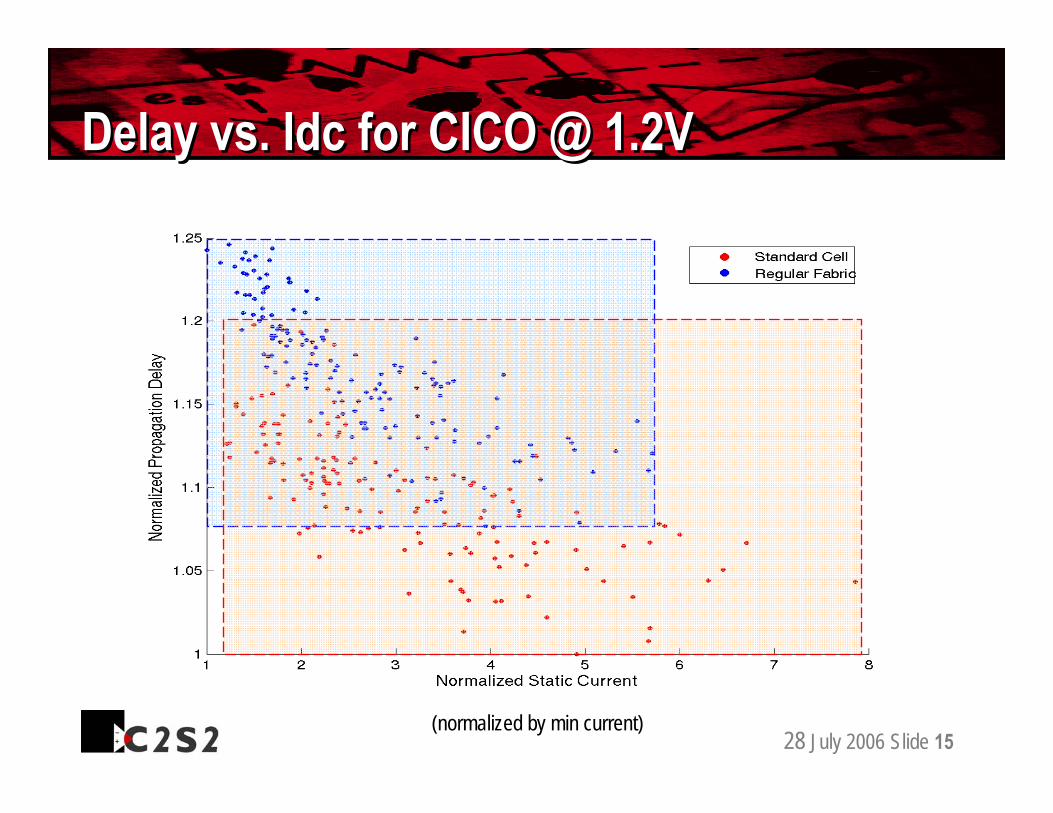
Delay vs. Idc for CICO @ 1.2VDelay vs. Idc for CICO @ 1.2V
(normalized by min current)
28 July 2006 Slide 16
www.c2s2.org
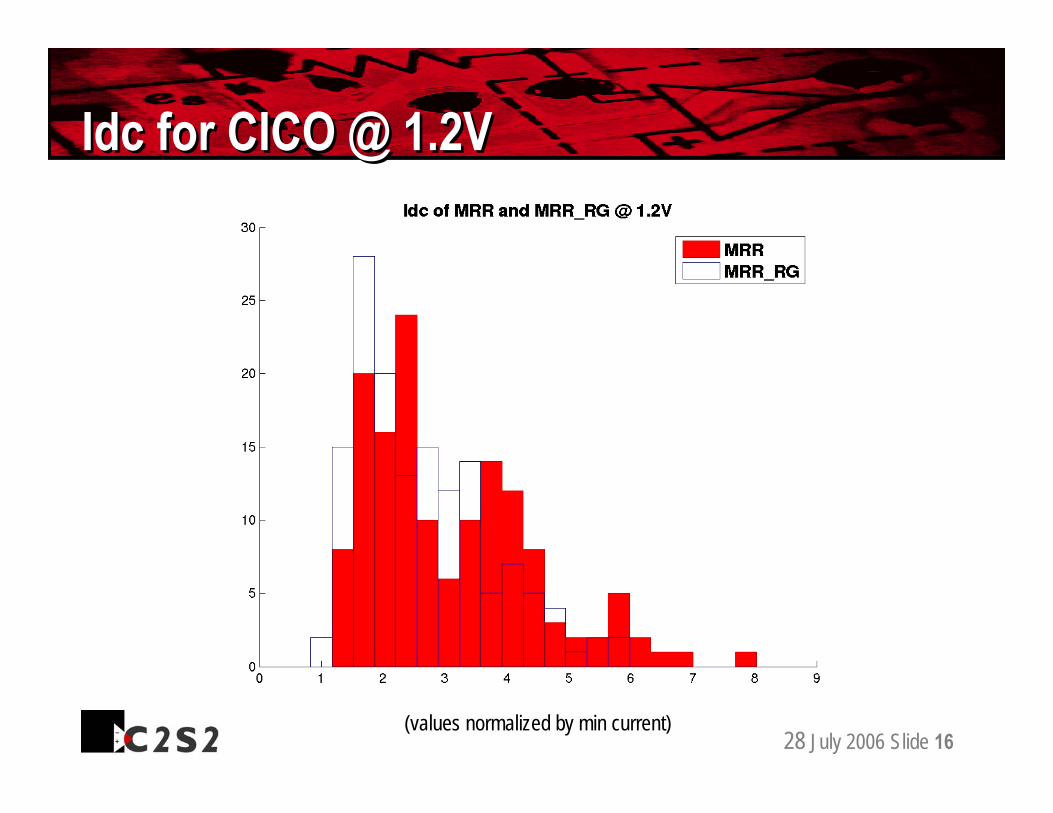
Idc for CICO @ 1.2VIdc for CICO @ 1.2V
(values normalized by min current)
28 July 2006 Slide 17
www.c2s2.org
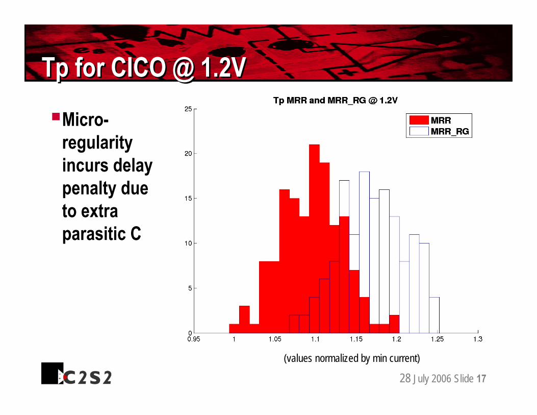
Tp for CICO @ 1.2VTp for CICO @ 1.2V
Micro-regularity incurs delay penalty due to extra parasitic C
(values normalized by min current)

28 July 2006 Slide 18
www.c2s2.org
Mean, Std. Deviation, and Coeff. Of Var.Mean, Std. Deviation, and Coeff. Of Var.Mean
Std. Deviation
assuming xi are independent, identically distributed samples
Coefficient of Variation is
( )∑=
−−
=N
iix
N 1
2
11 μσ
∑=
=N
iix
N 1
1μ
μσ

28 July 2006 Slide 19
www.c2s2.org
Static Current Comparisons (CICO)Static Current Comparisons (CICO)Mean Static Current
1.0
2.0
3.0
4.0
5.0
6.0
7.0
8.0
0.8 0.9 1 1.1 1.2 1.3 1.4Vdd (V)
Nor
mal
ized
Sta
tic
Cur
rent
Standard Cell
Regular Fabric
Standard Deviation
1.02.03.04.05.06.07.08.09.0
10.0
0.8 0.9 1 1.1 1.2 1.3 1.4Vdd (V)
Nor
mal
ized
Sta
ndar
d D
evia
tion
Standard Cell
Regular Fabric
Coefficient of Variation
1.00
1.05
1.10
1.15
1.20
1.25
1.30
0.8 0.9 1 1.1 1.2 1.3 1.4
Vdd (V)
Nor
mal
ized
Coe
ffici
ent o
f Va
riatio
n
Standard CellRegular Fabric
σ/μ

28 July 2006 Slide 20
www.c2s2.org
Propagation Delay Comparison (CICO)Propagation Delay Comparison (CICO)Mean Propagational Delay
1.0
1.5
2.0
2.5
3.0
3.5
4.0
4.5
5.0
0.8 0.9 1 1.1 1.2 1.3 1.4
Vdd (V)
Nor
mal
ized
Pro
paga
tiona
l D
elay
Standard CellRegular Fabric
Standard Deviation
1.0
2.0
3.0
4.0
5.0
6.0
7.0
8.0
9.0
0.8 0.9 1 1.1 1.2 1.3 1.4
Vdd (V)
Nor
mal
ized
Sta
ndar
d D
evia
tion
Standard CellRegular Fabric
Coefficient of Variation
1.00
1.10
1.20
1.30
1.40
1.50
1.60
1.70
1.80
1.90
2.00
0.8 0.9 1 1.1 1.2 1.3 1.4Vdd (V)
Nor
mal
ized
Coe
ffici
ent o
f Va
riatio
n
Standard CellRegular Fabric
Slightly higher nominal delay expected due to increased parasitics for pushed-rule regular fabric adder

28 July 2006 Slide 21
www.c2s2.org
Variations - Tp per gate @ Vdd = 1.2VVariations - Tp per gate @ Vdd = 1.2V
Standard cell mirror adderμ= 1.000 σ = 0.0371
Regular mirror adderμ = 1.025 σ = 0.0327
Wafermaps of abs(x - μ), normalized by max value
0
0.1
0.2
0.3
0.4
0.5
0.6
0.7
0.8
0.9
1
-6 -4 -2 0 2 4 6
-6
-4
-2
0
2
4
6
-6 -4 -2 0 2 4 6
-6
-4
-2
0
2
4
6

28 July 2006 Slide 22
www.c2s2.org
Variations – Idc per gate @ Vdd = 1.2VVariations – Idc per gate @ Vdd = 1.2V
Standard cell mirror adderμ= 1.000 σ = 0.4224
Regular mirror adderμ = 0.7213 σ = 0.2920
Wafermaps of abs(x - μ), normalized by max value
-6 -4 -2 0 2 4 6
-6
-4
-2
0
2
4
6
-6 -4 -2 0 2 4 6
-6
-4
-2
0
2
4
6
0
0.1
0.2
0.3
0.4
0.5
0.6
0.7
0.8
0.9
1

28 July 2006 Slide 23
www.c2s2.org
Outlier Count (Tp)Outlier Count (Tp)
Non-Regular mirror adder (all paths)# of outliers = 20
Regular mirror adder (all paths)# of outliers = 0
-6 -4 -2 0 2 4 6
-6
-4
-2
0
2
4
6
0
1
2
3
4
5
6
7
-6 -4 -2 0 2 4 6
-6
-4
-2
0
2
4
6
Count of outlyers beyond 3σ
σ = 0.0371 σ = 0.0327

28 July 2006 Slide 24
www.c2s2.org
Outlier Count (Idc)Outlier Count (Idc)
Non-Regular mirror adder (all paths)# of outliers = 22
Regular mirror adder (all paths)# of outliers = 12
Count of outliers beyond 3σ
-6 -4 -2 0 2 4 6
-6
-4
-2
0
2
4
6
0
1
2
3
4
5
6
7
-6 -4 -2 0 2 4 6
-6
-4
-2
0
2
4
6
σ = 0.4224 σ = 0.2920

28 July 2006 Slide 25
www.c2s2.org
ObservationsObservationsAny difference is due solely to micro-regularity of layout
Both designs are macro-regularImplementations have identical transistor topology and sizing
Difference in spread is most prominent in IdcExponentially dependent on gate length
We expect a greater variability impact when comparing macro-regularity differences

28 July 2006 Slide 26
www.c2s2.org
Macro-Regular Logic BricksMacro-Regular Logic BricksRecently proposed macro-regular design via regular bricks
Less cell-to-cell variation, as in SRAM bit-cellsTotal number of geometry patterns dramatically reduced
Provides known pattern neighborhood to adjacent bricksTighter characterization with known electrical environments
Micro-regularlogic
r
Micro-regularlogic
Micro-regularlogic
well-characterized, predictable pattern environments like memories

28 July 2006 Slide 27
www.c2s2.org
Big enough to satisfy optical proximity constraintsSmall enough to allow characterization and optimizationSpecific enough to minimize wasted logicGeneric enough to allow reuse over multiple logic functions
Optimal Brick SizeOptimal Brick Size
Brick Size
Total Area Small generic cells; (micro-regularity
penalty)
Big, generic bricks(wasted logic)
FewerPatterns
LogicEfficiency

28 July 2006 Slide 28
www.c2s2.org
Experimental FlowExperimental Flow

28 July 2006 Slide 29
www.c2s2.org
65nm Low Power CMOSStd Cell Spec Design:
16KB D cache, 32KB I cache250MHz worst caseArea: 1.1323 mm2
Bricks derived from7 fixed-size primitives3 Flip Flop typesVarious INV sizes for buffering16 fixed-size application-specific bricks
ARM9 ImplementationARM9 Implementation
ICache
MMU
DCache
Identical block footprint area for bricks and
std cell designs

28 July 2006 Slide 30
www.c2s2.org
ARM9 Implementation ResultsARM9 Implementation ResultsStd cells based on full sizing and resynthesis using complete library40% more buffer area for bricks design due to sizing limitationsDoes not measure potential improvement in parametric yield
99.4718.40Regular Bricks (using primitive mapping)
105.4016.90Primitives (on grid)
100.0025.17Standard Cells (not on grid)
Relative WC Timing (%)Silicon Whitespace (%)
Brick design has slightly less whitespace but fewer nets to routeSimulation results do not capture improvement in control of variations, or improvement with Brick-specific synthesis and flow

28 July 2006 Slide 31
www.c2s2.org
Normalized Leff comparison based on ACLV simulations at nominal process conditions for DFFs:
ACLV comparisonACLV comparison
3σµ
0.56921.0000.99051.000
FEOL push-rule BricksStd Cells

28 July 2006 Slide 32
www.c2s2.org
Regularity-Friendly CircuitsRegularity-Friendly CircuitsCan further consider circuits and topologies which better match regular brick methodology and constraintsExample:
New DFF topology can reduce footprint, require only single clk polarity, and provide 20-40% improvement in speed

28 July 2006 Slide 33
www.c2s2.org
Statistical OptimizationStatistical OptimizationBricks can be statistically optimized for sizing w.r.t. variationsWe expect that macro-regularity of bricks vs. standard cells will provide substantial improvement in predictability
Adjacent stress
Active corner
Random DopantSTI-Poly distance stress
Contact placement
Poly corner

28 July 2006 Slide 34
www.c2s2.org
Conclusions and Future DirectionsConclusions and Future DirectionsForms of Regular Fabrics appear to offer advantages beginning at 65nm node
Benefits of reduced design margins have yet to be fully measuredWith limited number of bricks we can optimize them for better control and prediction of variations
Both systematic (those which we can model) and random (those which cannot completely model) variations can be reducedCan carefully design bricks to reduce sensitivity to random variations
![CHAPTER 5 THE ALLARD REGULARITY THEOREMmaths-proceedings.anu.edu.au/.../CMAProcVol3-Chapter5.pdfCHAPTER 5 THE ALLARD REGULARITY THEOREM Here we discuss Allard's ([AWl]) regularity](https://static.fdocuments.in/doc/165x107/5fb2cc5e95482068621741eb/chapter-5-the-allard-regularity-theoremmaths-chapter-5-the-allard-regularity-theorem.jpg)


![T2 · 2019. 8. 1. · 310 M.N. MUKHERJEE AND S.P. SINHA regularity were also defined in [6]. Wecharacterize fuzzy regularity and these weaker forms of fuzzy regularity in terms of](https://static.fdocuments.in/doc/165x107/60b0546db5896d7af80bbfee/t2-2019-8-1-310-mn-mukherjee-and-sp-sinha-regularity-were-also-defined.jpg)