Reflection High-Energy Electron Diffraction as a Tool for...
29
In: “In Situ Process Diagnostics and Intelligent Materials Processing”, edited by O. Auciello and A.R. Krauss, (Wiley Science, 2000). pp.29-56 Reflection High-Energy Electron Diffraction as a Tool for Real-Time Characterization of Growth of Complex Oxides IVAN BOZOVIC Oxxel GmbH, Bremen, Germany J. N. ECKSTEIN University of Illinois, Urbana, Illinois NATASHA BOZOVIC San Jose State University, San Jose, California 2.1 INTRODUCTION An attachment for reflection high-energy electron diffraction (RHEED) is frequently found on ultrahigh vacuum systems, such as molecular beam epitaxy (MBE) machines, used for the growth of epitaxial thin films. In most cases, these are used to study semiconductors such as Si, Ge, or GaAs, and hence most RHEED treatises focus on these materials. However, after the discovery of high- temperature superconductivity in LaBaCuO in 1986, a number of MBE systems have been designed and built specifically for deposition of thin films of cuprates. Virtually each of these machines contains a RHEED accessory. More recently, some of these MBE systems have been employed also to synthesize other interesting oxides: ferroelectrics (e.g., titanates) and ferromagnets (e.g., manganites). Given the short history of RHEED study of oxides, it is not surprising that it has not been reviewed yet in the literature, except for two brief expositions (Bozovic and Eckstein, 1995; Bozovic et al., 1997). Thus, we feel that there is some motivation for this chapter, which is an expanded version of these two earlier articles. Our own work has been in this area (see Eckstein et al., 1992, 1994), and hence so are our examples. For a good general introduction to RHEED, see Lagally (1985) and Lagally and Savage, 1993; there one can find a clear explanation of electron diffraction, the reciprocal-space representation, reflection from imperfect surfaces, and so on. 2.2 READING RHEED PATTERNS
Transcript of Reflection High-Energy Electron Diffraction as a Tool for...

In: “In Situ Process Diagnostics and Intelligent Materials Processing”, edited by O. Auciello and A.R. Krauss,(Wiley Science, 2000). pp.29-56
Reflection High-Energy ElectronDiffraction as a Tool for Real-TimeCharacterization of Growth ofComplex OxidesIVAN BOZOVICOxxel GmbH, Bremen, Germany
J. N. ECKSTEINUniversity of Illinois, Urbana, Illinois
NATASHA BOZOVICSan Jose State University, San Jose, California
2.1 INTRODUCTION
An attachment for reflection high-energy electron diffraction (RHEED) is frequently foundon ultrahigh vacuum systems, such as molecular beam epitaxy (MBE) machines, used forthe growth of epitaxial thin films. In most cases, these are used to study semiconductorssuch as Si, Ge, or GaAs, and hencemost RHEED treatises focus on these materials. However, after the discovery of high-temperature superconductivity in LaBaCuO in 1986, a number of MBE systems have beendesigned and built specifically for deposition of thin films of cuprates. Virtually each ofthese machines contains a RHEED accessory. Morerecently, some of these MBE systems have been employed also to synthesize otherinteresting oxides: ferroelectrics (e.g., titanates) and ferromagnets (e.g., manganites).Given the short history of RHEED study of oxides, it is not surprising that it has not beenreviewed yet in the literature, except for two brief expositions (Bozovic and Eckstein, 1995;Bozovic et al., 1997). Thus, we feel that there is some motivation for this chapter, which isan expanded version of these two earlier articles. Our own work has been in this area (seeEckstein et al., 1992, 1994), and hence so are our examples. For a good generalintroduction to RHEED, see Lagally (1985) and Lagally and Savage, 1993; there one canfinda clear explanation of electron diffraction, the reciprocal-space representation, reflectionfrom imperfect surfaces, and so on.
2.2 READING RHEED PATTERNS

30
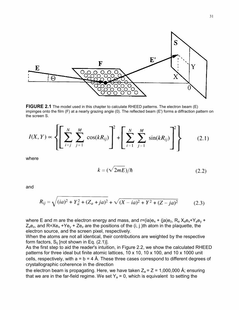
Reflection high-energy electron diffraction patterns result from and contain detailedinformation about the crystalline properties of surfaces. In the field of oxide thin films,RHEED analysis is currently used mainly for qualitative information-simply to watchdiffraction patterns and to note their evolution in time. Even this can be quite useful andcan reveal atomic scale information about how a sample is growing by reference tophenomenology developed by experience. As we discuss below, it is possible todistinguish a flat, two-dimensional (2D) surface from one having (usually unwanted) three-dimensional (3D)nanoparticles. For the time being, we consider the former case.At least in principle, the diagnostic value of RHEED monitoring could be substantiallyincreased if it were supplemented by a quantitative analysis of the entire RHEED pattern.Ultimately, one could envision a numerical routine that solves the inverse problem in realtime, that is, computes the real-space atomic arrangement on the surface thatcorresponds to a given RHEED image. Unfortunately, in the general case, this task isintractable because phase information about the electron wave function is missing.In many cases, however, it is possible to begin with a plausible guess as to the atomicsurface configuration and to use the RHEED pattern to refine this guess. We haveperformed numerical simulations of some 2D surfaces in which we started by postulating a"reasonable" surface structure, calculated the corresponding RHEED pattern, andcompared it to the experimentally observed image. While clearly limited in scope, thissimple approach still enables one to extract more quantitative information about thecrystallographic arrangement, extent of long-range order on the surface, roughness, andso on. In the long run, this may help to develop more sophisticated methods of analysis.In Figure 2.1, we show a schematic of a typical calculation and of an experimental RHEEDsetup. The electron beam (E) impinges onto the film surface (F) at a nearly grazing angle(N), and is reflected (E') onto the screen (S).The electron beam is coherent over several thousand angstroms and is nearlymonoenergetic; in our case, the electron energy is typically K8.5-10.0 keV. The filmsurface is approximated as a perfect but finite rectangular N x M array of atoms with thelattice periods a and b, respectively.Since typically aKbK4 � >> Ue K0.15 �, the electrons are strongly diffracted, and oneexpects to see multiple interference maxima on the screen. In this case, the refinementprocedure provides an estimate of the size of in-plane crystallographic coherence, that is,an estimate of the numbers N and M.To calculate the diffraction pattern, we sum the scattering contributions from all the atoms.The resulting intensity distribution on the screen is given by
31
FIGURE 2.1 The model used in this chapter to calculate RHEED patterns. The electron beam (E)impinges onto the film (F) at a nearly grazing angle (0). The reflected beam (E') forms a diffraction pattern onthe screen S.
where
and
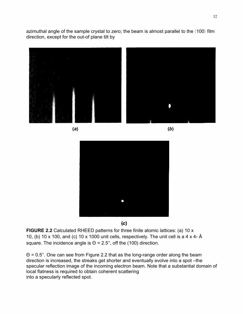
where E and m are the electron energy and mass, and r=(ia)ex + (ja)ez, Ra Xaex+Yaey +Zaez, and R=Xex +Yey + Zez are the positions of the (i, j )th atom in the plaquette, theelectron source, and the screen pixel, respectively.When the atoms are not all identical, their contributions are weighted by the respectiveform factors, Sij [not shown in Eq. (2.1)].As the first step to aid the reader's intuition, in Figure 2.2, we show the calculated RHEEDpatterns for three ideal but finite atomic lattices, 10 x 10, 10 x 100, and 10 x 1000 unitcells, respectively, with a = b = 4 �. These three cases correspond to different degrees ofcrystallographic coherence in the directionthe electron beam is propagating. Here, we have taken Za = Z = 1,000,000 �; ensuringthat we are in the far-field regime. We set Ya = 0, which is equivalent to setting the
32
azimuthal angle of the sample crystal to zero; the beam is almost parallel to the H100I filmdirection, except for the out-of plane tilt by
FIGURE 2.2 Calculated RHEED patterns for three finite atomic lattices: (a) 10 x10, (b) 10 x 100, and (c) 10 x 1000 unit cells, respectively. The unit cell is a 4 x 4-��square. The incidence angle is N = 2.5�, off the (100) direction.
N = 0.5�. One can see from Figure 2.2 that as the long-range order along the beamdirection is increased, the streaks get shorter and eventually evolve into a spot –thespecular reflection image of the incoming electron beam. Note that a substantial domain oflocal flatness is required to obtain coherent scatteringinto a specularly reflected spot.
33
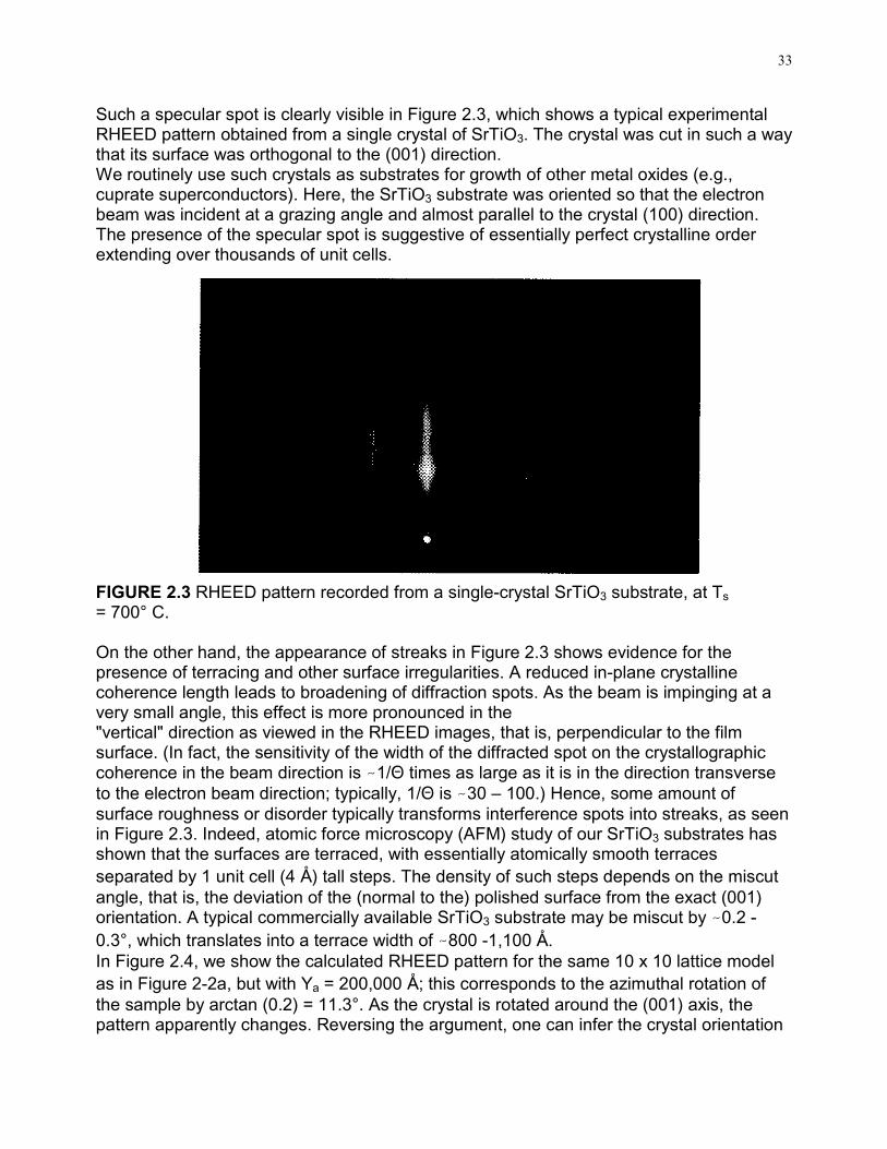
Such a specular spot is clearly visible in Figure 2.3, which shows a typical experimentalRHEED pattern obtained from a single crystal of SrTiO3. The crystal was cut in such a waythat its surface was orthogonal to the (001) direction.We routinely use such crystals as substrates for growth of other metal oxides (e.g.,cuprate superconductors). Here, the SrTiO3 substrate was oriented so that the electronbeam was incident at a grazing angle and almost parallel to the crystal (100) direction.The presence of the specular spot is suggestive of essentially perfect crystalline orderextending over thousands of unit cells.
FIGURE 2.3 RHEED pattern recorded from a single-crystal SrTiO3 substrate, at Ts= 700° C.
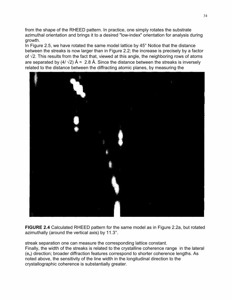
On the other hand, the appearance of streaks in Figure 2.3 shows evidence for thepresence of terracing and other surface irregularities. A reduced in-plane crystallinecoherence length leads to broadening of diffraction spots. As the beam is impinging at avery small angle, this effect is more pronounced in the"vertical" direction as viewed in the RHEED images, that is, perpendicular to the filmsurface. (In fact, the sensitivity of the width of the diffracted spot on the crystallographiccoherence in the beam direction is J1/N times as large as it is in the direction transverseto the electron beam direction; typically, 1/N is J30 – 100.) Hence, some amount ofsurface roughness or disorder typically transforms interference spots into streaks, as seenin Figure 2.3. Indeed, atomic force microscopy (AFM) study of our SrTiO3 substrates hasshown that the surfaces are terraced, with essentially atomically smooth terracesseparated by 1 unit cell (4 �) tall steps. The density of such steps depends on the miscutangle, that is, the deviation of the (normal to the) polished surface from the exact (001)orientation. A typical commercially available SrTiO3 substrate may be miscut by J0.2 -0.3°, which translates into a terrace width of J800 -1,100 �.In Figure 2.4, we show the calculated RHEED pattern for the same 10 x 10 lattice modelas in Figure 2-2a, but with Ya = 200,000 �; this corresponds to the azimuthal rotation ofthe sample by arctan (0.2) = 11.3°. As the crystal is rotated around the (001) axis, thepattern apparently changes. Reversing the argument, one can infer the crystal orientation
34
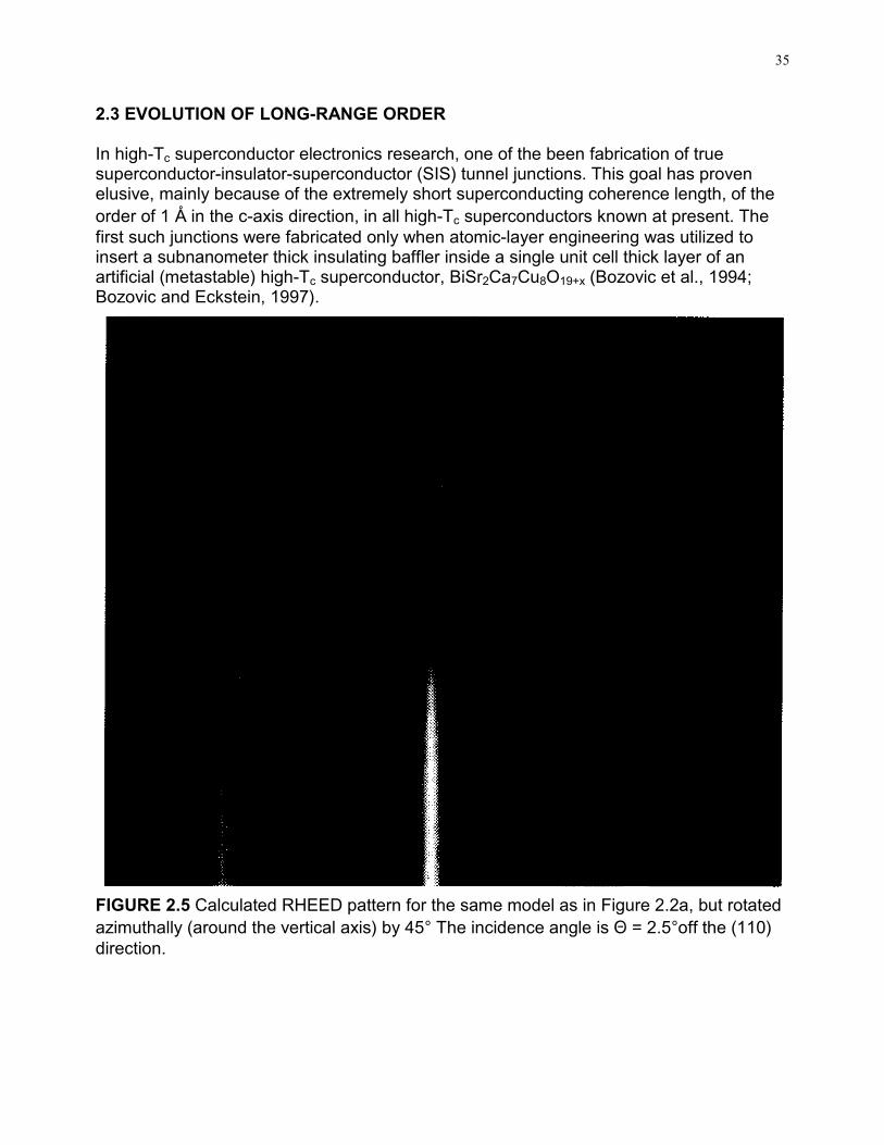
from the shape of the RHEED pattern. In practice, one simply rotates the substrateazimuthal orientation and brings it to a desired "low-index" orientation for analysis duringgrowth.In Figure 2.5, we have rotated the same model lattice by 45° Notice that the distancebetween the streaks is now larger than in Figure 2.2; the increase is precisely by a factorof √2. This results from the fact that, viewed at this angle, the neighboring rows of atomsare separated by (4/ √2) � = 2.8 �. Since the distance between the streaks is inverselyrelated to the distance between the diffracting atomic planes, by measuring the
FIGURE 2.4 Calculated RHEED pattern for the same model as in Figure 2.2a, but rotatedazimuthally (around the vertical axis) by 11.3°.
streak separation one can measure the corresponding lattice constant.Finally, the width of the streaks is related to the crystalline coherence range in the lateral(ex) direction; broader diffraction features correspond to shorter coherence lengths. Asnoted above, the sensitivity of the line width in the longitudinal direction to thecrystallographic coherence is substantially greater.
35
2.3 EVOLUTION OF LONG-RANGE ORDER
In high-Tc superconductor electronics research, one of the been fabrication of truesuperconductor-insulator-superconductor (SIS) tunnel junctions. This goal has provenelusive, mainly because of the extremely short superconducting coherence length, of theorder of 1 � in the c-axis direction, in all high-Tc superconductors known at present. Thefirst such junctions were fabricated only when atomic-layer engineering was utilized toinsert a subnanometer thick insulating baffler inside a single unit cell thick layer of anartificial (metastable) high-Tc superconductor, BiSr2Ca7Cu8O19+x (Bozovic et al., 1994;Bozovic and Eckstein, 1997).
FIGURE 2.5 Calculated RHEED pattern for the same model as in Figure 2.2a, but rotatedazimuthally (around the vertical axis) by 45� The incidence angle is N = 2.5�off the (110)direction.

36
Since in the cuprates the in-plane coherence length is much longer (20-30��), a number ofgroups focused their efforts on deposition of so-called a-axis oriented YBa2Cu3O7 films,with CuO2 planes perpendicular to the substrate and the film surface (Eom et al., 1990,1991; Barrier et al., 1991; Hashimoto et al., 1992; Umezawa et al., 1993; Takahashi et al.,1991, 1992; Suzuki et al., 1993, 1994). The key technological problems that theyencountered were (1) surface roughness and (2) formation of secondary-phase (mostlyCuO) precipitates.Both of these are deleterious to fabrication of tunnel junctions, since rough surfaces makeit difficult to deposit ultrathin yet continuous insulator barriers without pinholes, which ifpresent would short the junctions and render them useless. The same is true for CuOgrains, which are conducting.To the best of our knowledge, no conclusive success has been reported so far in growingatomically smooth a-axis oriented YBa2Cu3O7 films without any secondary-phaseprecipitates. In what follows, we will show how we have achieved this goal using atomic-layer MBE deposition technique and continuous RHEED monitoring, which guided usthrough the complex phase diagram of DyBa2Cu3O7-x. (Instead of Y, we used Dy becauseof its higher vapor pressure.)
37
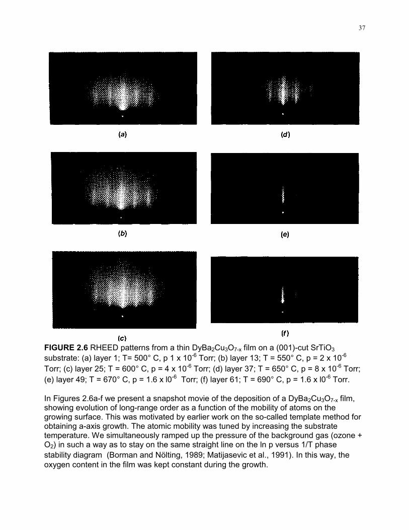
FIGURE 2.6 RHEED patterns from a thin DyBa2Cu3O7-x film on a (001)-cut SrTiO3
substrate: (a) layer 1; T= 500� C, p 1 x 10⁻⁶ Torr; (b) layer 13; T = 550� C, p = 2 x 10⁻⁶
Torr; (c) layer 25; T = 600��C, p = 4 x 10⁻⁶ Torr; (d) layer 37; T = 650� C, p = 8 x 10⁻⁶ Torr;(e) layer 49; T = 670��C, p = 1.6 x l0-6 Torr; (f) layer 61; T = 690���, p = 1.6 x l0-6 Torr.
In Figures 2.6a-f we present a snapshot movie of the deposition of a DyBa2Cu3O7-x film,showing evolution of long-range order as a function of the mobility of atoms on thegrowing surface. This was motivated by earlier work on the so-called template method forobtaining a-axis growth. The atomic mobility was tuned by increasing the substratetemperature. We simultaneously ramped up the pressure of the background gas (ozone +O2) in such a way as to stay on the same straight line on the ln p versus 1/T phasestability diagram (Borman and N�lting, 1989; Matijasevic et al., 1991). In this way, theoxygen content in the film was kept constant during the growth.
38
At the lowest temperature, 500��C (Fig. 2.6a), after depositing 1 unit cell thick layer ofDyBa2Cu3O7-x, we saw broadened 0, ±1, ±2 streaks together with a bright specularreflection; the surface remained flat but disordered. The streaks became sharper at 550�C (Fig. 2.6b). At 600��C (Fig. 2.6c), one starts to see faint lines in between the mainstreaks. These side bands became more visible at 650��C (Fig. 2.6d), and rather intenseand sharp at 670��C (Fig. 2.6e) and 690��C (Fig. 2.6f). These are one-third-order streaks-the diffraction signatures of strong periodicity with an in-plane lattice constant three timeslarger (J11.7 �) than the original (3.9 �) lattice constant. This is direct crystallographicevidence of growth of an a axis oriented DyBa2Cu3O7-x film. Reemergence of the strongspecular reflection in Figure 2.6e and f signals simultaneous flattening out of the surface.
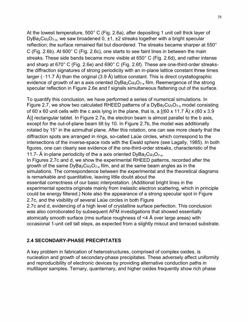
To quantify this conclusion, we have performed a series of numerical simulations. InFigure 2.7, we show two calculated RHEED patterns of a DyBa2Cu3O7-x model consistingof 60 x 60 unit cells with the c axis lying in the plane, that is, a [(60 x 11.7 �) x (60 x 3.9�)] rectangular tablet. In Figure 2.7a, the electron beam is almost parallel to the b axis,except for the out-of-plane beam tilt by 10. In Figure 2.7b, the model was additionallyrotated by 15� in the azimuthal plane. After this rotation, one can see more clearly that thediffraction spots are arranged in rings, so-called La�e circles, which correspond to theintersections of the inverse-space rods with the Ewald sphere (see Lagally, 1985). In bothfigures, one can cleariy see evidence of the one-third-order streaks, characteristic of the11.7-�� in-plane periodicity of the a axis oriented DyBa2Cu3O7-x.In Figures 2.7c and d, we show the experimental RHEED patterns, recorded after thegrowth of the same DyBa2Cu3O7-x film, and at the same beam angles as in thesimulations. The correspondence between the experimental and the theoretical diagramsis remarkable and quantitative, leaving little doubt about theessential correctness of our basic interpretation. (Additional bright lines in theexperimental spectra originate mainly from inelastic electron scattering, which in principlecould be energy filtered.) Note also the appearance of a strong specular spot in Figure2.7c, and the visibility of several La�e circles in both Figure2.7c and d, evidencing of a high level of crystalline surface perfection. This conclusionwas also corroborated by subsequent AFM investigations that showed essentiallyatomically smooth surface (rms surface roughness of <4 � over large areas) withoccasional 1-unit cell tall steps, as expected from a slightly miscut and terraced substrate.
2.4 SECONDARY-PHASE PRECIPITATES
A key problem in fabrication of heterostructures, comprised of complex oxides, isnucleation and growth of secondary-phase precipitates. These adversely affect uniformityand reproducibility of electronic devices by providing alternative conduction paths inmultilayer samples. Ternary, quanternary, and higher oxides frequently show rich phase
39
FIGURE 2.7 (a) Calculated RHEED pattern for a perfect a axis oriented DyBa2Cu3O7-xfilm; the beam is tilted by 10 off (100). (b) The same but with the model rotated azimuthallyby 15°. (c) Experimentally observed RHEED patterns of a thin DyBa2Cu3O7-x film on a(100)-cut SrTiO3 substrate; end of growth, layer 126. (d) The same but with the samplerotated azimuthally by J15° off the (100) direction.
diagrams, containing many compounds, and these even vary with the growth conditions.The stoichiometry that is optimal for single-phase thin-film growth need not be the sameas the one found in bulk single crystals. Furthermore, it is unknown a priori in most cases.Overall, heterogeneous growth often occurs in oxide films, and grains of an undesired(secondary) phases are embedded in the matrix of the targeted phase. For multilayerdevices, this must be understood and eliminated. If such precipitates are detected as soonas they are nucleated, we have found that it is possible to dissolve them by adjusting the
40
stoichiometry in the subsequent layers to account for the incorrect initial composition.Thus RHEED provides an unparalleled tool for accurate phase determination and control.
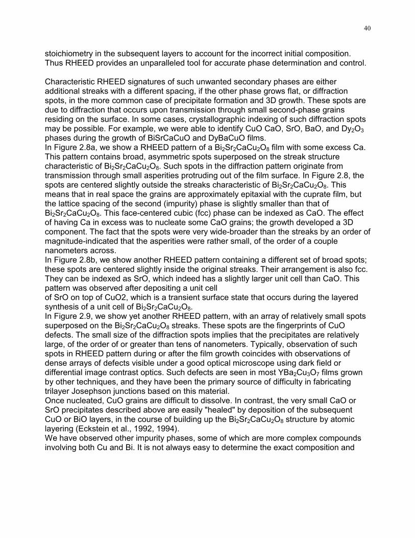
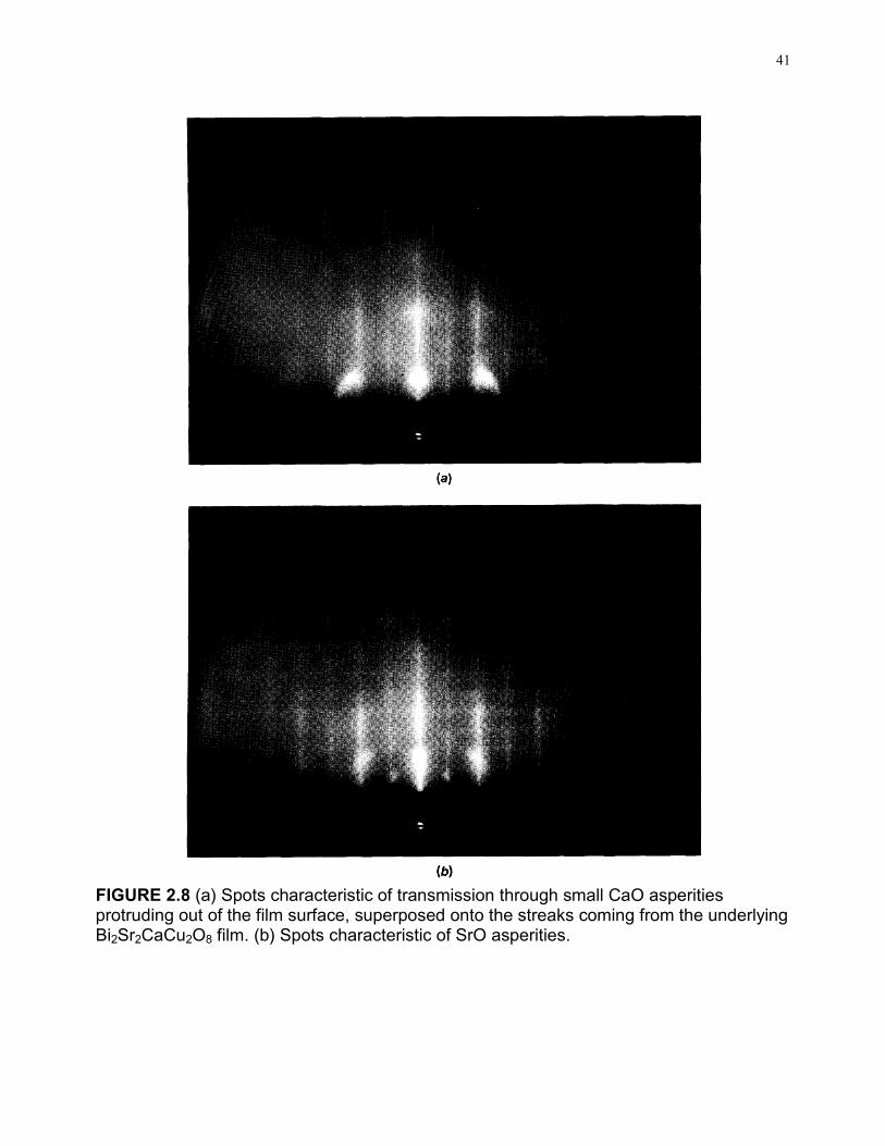
Characteristic RHEED signatures of such unwanted secondary phases are eitheradditional streaks with a different spacing, if the other phase grows flat, or diffractionspots, in the more common case of precipitate formation and 3D growth. These spots aredue to diffraction that occurs upon transmission through small second-phase grainsresiding on the surface. In some cases, crystallographic indexing of such diffraction spotsmay be possible. For example, we were able to identify CuO CaO, SrO, BaO, and Dy2O3phases during the growth of BiSrCaCuO and DyBaCuO films.In Figure 2.8a, we show a RHEED pattern of a Bi2Sr2CaCu2O8 film with some excess Ca.This pattern contains broad, asymmetric spots superposed on the streak structurecharacteristic of Bi2Sr2CaCu2O8. Such spots in the diffraction pattern originate fromtransmission through small asperities protruding out of the film surface. In Figure 2.8, thespots are centered slightly outside the streaks characteristic of Bi2Sr2CaCu2O8. Thismeans that in real space the grains are approximately epitaxial with the cuprate film, butthe lattice spacing of the second (impurity) phase is slightly smaller than that ofBi2Sr2CaCu2O8. This face-centered cubic (fcc) phase can be indexed as CaO. The effectof having Ca in excess was to nucleate some CaO grains; the growth developed a 3Dcomponent. The fact that the spots were very wide-broader than the streaks by an order ofmagnitude-indicated that the asperities were rather small, of the order of a couplenanometers across.In Figure 2.8b, we show another RHEED pattern containing a different set of broad spots;these spots are centered slightly inside the original streaks. Their arrangement is also fcc.They can be indexed as SrO, which indeed has a slightly larger unit cell than CaO. Thispattern was observed after depositing a unit cellof SrO on top of CuO2, which is a transient surface state that occurs during the layeredsynthesis of a unit cell of Bi2Sr2CaCu2O8.In Figure 2.9, we show yet another RHEED pattern, with an array of relatively small spotssuperposed on the Bi2Sr2CaCu2O8 streaks. These spots are the fingerprints of CuOdefects. The small size of the diffraction spots implies that the precipitates are relativelylarge, of the order of or greater than tens of nanometers. Typically, observation of suchspots in RHEED pattern during or after the film growth coincides with observations ofdense arrays of defects visible under a good optical microscope using dark field ordifferential image contrast optics. Such defects are seen in most YBa2Cu3O7 films grownby other techniques, and they have been the primary source of difficulty in fabricatingtrilayer Josephson junctions based on this material.Once nucleated, CuO grains are difficult to dissolve. In contrast, the very small CaO orSrO precipitates described above are easily "healed" by deposition of the subsequentCuO or BiO layers, in the course of building up the Bi2Sr2CaCu2O8 structure by atomiclayering (Eckstein et al., 1992, 1994).We have observed other impurity phases, some of which are more complex compoundsinvolving both Cu and Bi. It is not always easy to determine the exact composition and
41
FIGURE 2.8 (a) Spots characteristic of transmission through small CaO asperitiesprotruding out of the film surface, superposed onto the streaks coming from the underlyingBi2Sr2CaCu2O8 film. (b) Spots characteristic of SrO asperities.
42
FIGURE 2.9 Spots characteristic of transmission through small CuO grains protruding outof the film surface are superposed onto the Bi2Sr2CaCu2O8 streaks.
structure of the secondary phases from RHEED alone, and in such cases one needs touse other surface analytical techniques.
2.5 SURFACE PLANARIZATION
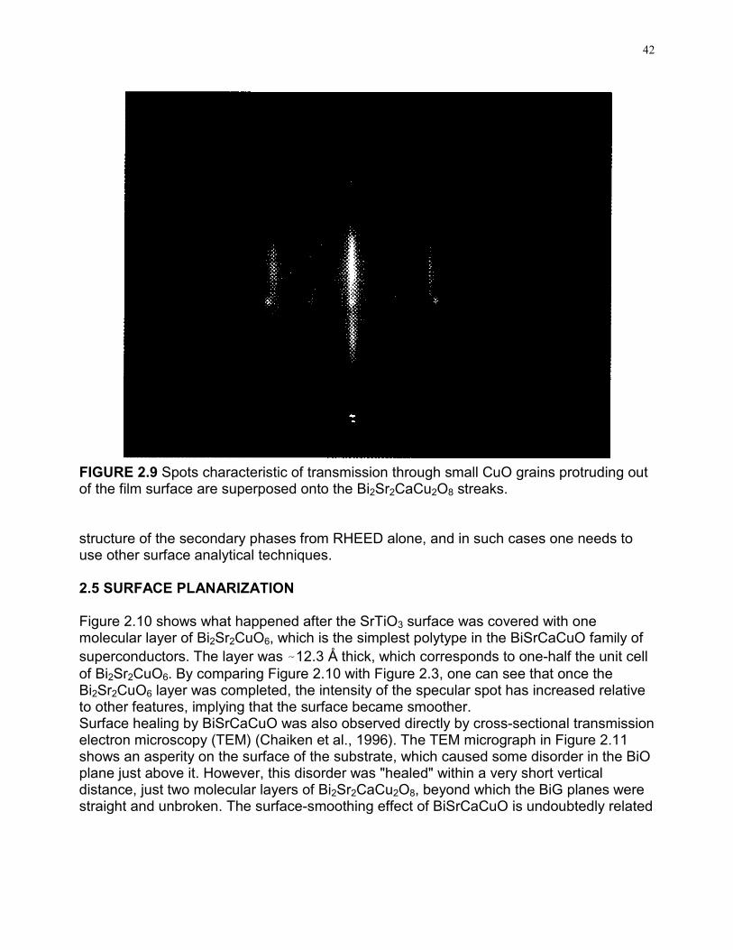
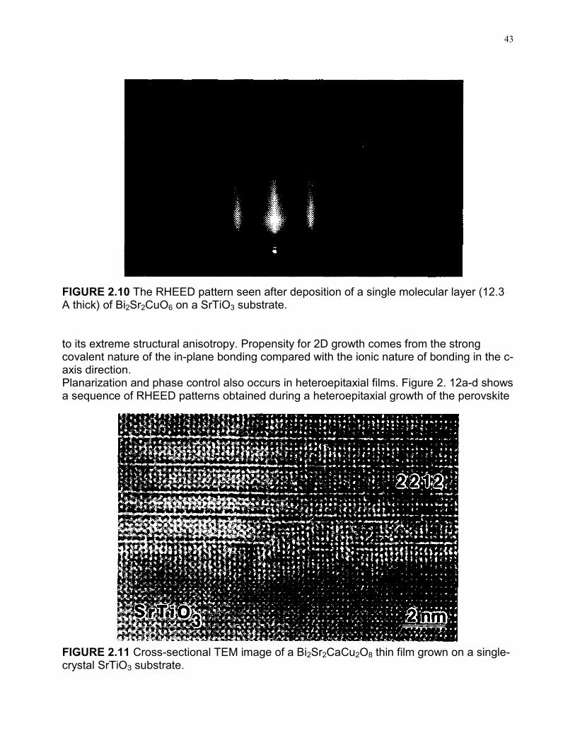
Figure 2.10 shows what happened after the SrTiO3 surface was covered with onemolecular layer of Bi2Sr2CuO6, which is the simplest polytype in the BiSrCaCuO family ofsuperconductors. The layer was J12.3 � thick, which corresponds to one-half the unit cellof Bi2Sr2CuO6. By comparing Figure 2.10 with Figure 2.3, one can see that once theBi2Sr2CuO6 layer was completed, the intensity of the specular spot has increased relativeto other features, implying that the surface became smoother.Surface healing by BiSrCaCuO was also observed directly by cross-sectional transmissionelectron microscopy (TEM) (Chaiken et al., 1996). The TEM micrograph in Figure 2.11shows an asperity on the surface of the substrate, which caused some disorder in the BiOplane just above it. However, this disorder was "healed" within a very short verticaldistance, just two molecular layers of Bi2Sr2CaCu2O8, beyond which the BiG planes werestraight and unbroken. The surface-smoothing effect of BiSrCaCuO is undoubtedly related
43
FIGURE 2.10 The RHEED pattern seen after deposition of a single molecular layer (12.3A thick) of Bi2Sr2CuO6 on a SrTiO3 substrate.
to its extreme structural anisotropy. Propensity for 2D growth comes from the strongcovalent nature of the in-plane bonding compared with the ionic nature of bonding in the c-axis direction.Planarization and phase control also occurs in heteroepitaxial films. Figure 2. 12a-d showsa sequence of RHEED patterns obtained during a heteroepitaxial growth of the perovskite
FIGURE 2.11 Cross-sectional TEM image of a Bi2Sr2CaCu2O8 thin film grown on a single-crystal SrTiO3 substrate.
44
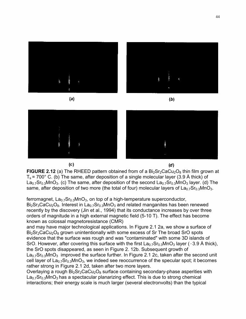
FIGURE 2.12 (a) The RHEED pattern obtained from of a Bi2Sr2CaCu2O8 thin film grown atTs = 700° C. (b) The same, after deposition of a single molecular layer (3.9 Å thick) ofLa0.7Sr0.3MnO3. (c) The same, after deposition of the second La0.7Sr0.3MnO3 layer. (d) Thesame, after deposition of two more (the total of four) molecular layers of La0.7Sr0.3MnO3.
ferromagnet, La0.7Sr0.3MnO3, on top of a high-temperature superconductor,Bi2Sr3CaCu2O8. Interest in La0.7Sr0.3MnO3 and related manganites has been renewedrecently by the discovery (Jin et al., 1994) that its conductance increases by over threeorders of magnitude in a high external magnetic field (5-10 T). The effect has becomeknown as colossal magnetoresistance (CMR)and may have major technological applications. In Figure 2.1 2a, we show a surface ofBi2Sr2CaCu2O8 grown unintentionally with some excess of Sr The broad SrO spotsevidence that the surface was rough and was "contaminated" with some 3D islands ofSrO. However, after covering this surface with the first La0.7Sr0.3MnO3 layer (J3.9 Å thick),the SrO spots disappeared, as seen in Figure 2. 12b. Subsequent growth ofLa0.7Sr0.3MnO3 improved the surface further. In Figure 2.1 2c, taken after the second unitcell layer of La0.7Sr0.3MnO3, we indeed see reoccurrence of the specular spot; it becomesrather strong in Figure 2.1 2d, taken after two more layers.Overlaying a rough Bi2Sr2CaCu2O8 surface containing secondary-phase asperities withLa0.7Sr0.3MnO3 has a spectacular planarizing effect. This is due to strong chemicalinteractions; their energy scale is much larger (several electronvolts) than the typical
45
thermal energy (1000 K or J0.1 eV) of the atoms on the surface. Imagine a chemistpouring onto the substrate minute quantities of different compounds to control thechemical reactions –but note that we are dealing with really minute quantities here,picograms at a time. And in our case, the chemistry is restricted to the surface; atoms arerather mobile on the free surface, while there is very little bulk diffusion, as evidenced byatomically sharp interfaces that are apparent in crossection TEM images of variousmultilayers and superlattices (Chaiken et al., 1996). Thanks to this capability to dissolveexcess SrO without affecting the rest of the film, it is relatively easy to fabricatesophisticated heterostructures comprised of Bi2Sr2CaCu2O8, La0.7Sr0.3MnO3, and otherrelated oxides, with virtually atomically perfect heterointerfaces.Such heterostructures are of substantial current interest in the context of spin-injectiondevices.
2.6 SUPERSTRUCTURES AND TWINNING
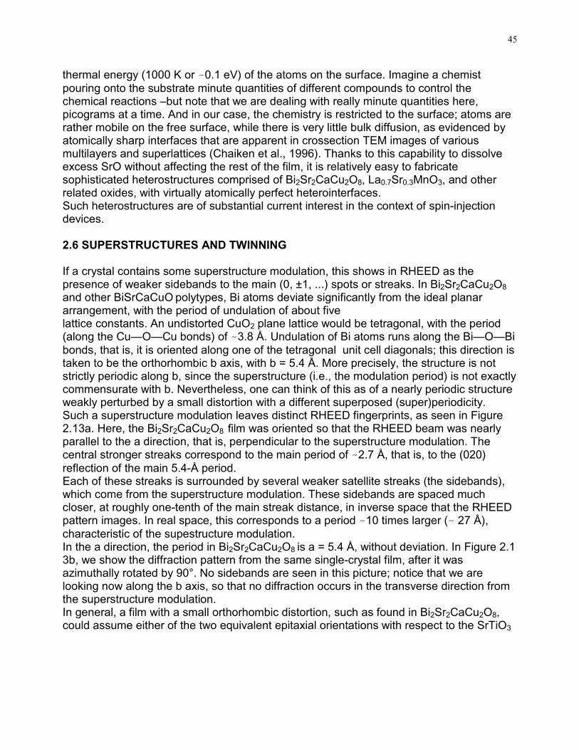
If a crystal contains some superstructure modulation, this shows in RHEED as thepresence of weaker sidebands to the main (0, ±1, ...) spots or streaks. In Bi2Sr2CaCu2O8and other BiSrCaCuO polytypes, Bi atoms deviate significantly from the ideal planararrangement, with the period of undulation of about fivelattice constants. An undistorted CuO2 plane lattice would be tetragonal, with the period(along the Cu—O—Cu bonds) of J3.8 Å. Undulation of Bi atoms runs along the Bi—O—Bibonds, that is, it is oriented along one of the tetragonal unit cell diagonals; this direction istaken to be the orthorhombic b axis, with b = 5.4 Å. More precisely, the structure is notstrictly periodic along b, since the superstructure (i.e., the modulation period) is not exactlycommensurate with b. Nevertheless, one can think of this as of a nearly periodic structureweakly perturbed by a small distortion with a different superposed (super)periodicity.Such a superstructure modulation leaves distinct RHEED fingerprints, as seen in Figure2.13a. Here, the Bi2Sr2CaCu2O8 film was oriented so that the RHEED beam was nearlyparallel to the a direction, that is, perpendicular to the superstructure modulation. Thecentral stronger streaks correspond to the main period of J2.7 Å, that is, to the (020)reflection of the main 5.4-Å period.Each of these streaks is surrounded by several weaker satellite streaks (the sidebands),which come from the superstructure modulation. These sidebands are spaced muchcloser, at roughly one-tenth of the main streak distance, in inverse space that the RHEEDpattern images. In real space, this corresponds to a period J10 times larger (J 27 Å),characteristic of the supestructure modulation.In the a direction, the period in Bi2Sr2CaCu2O8 is a = 5.4 Å, without deviation. In Figure 2.13b, we show the diffraction pattern from the same single-crystal film, after it wasazimuthally rotated by 90°. No sidebands are seen in this picture; notice that we arelooking now along the b axis, so that no diffraction occurs in the transverse direction fromthe superstructure modulation.In general, a film with a small orthorhombic distortion, such as found in Bi2Sr2CaCu2O8,could assume either of the two equivalent epitaxial orientations with respect to the SrTiO3
46
FIGURE 2.13 (a) The RHEED pattern from an untwinned Bi2Sr2CaCu2O8 film. Theelectron beam is incident along the b axis. The sidebands originate from superstructuremodulation. (b) The pattern from the same crystal rotated azimuthally by 90°. The beam isincident along the a axis.
47
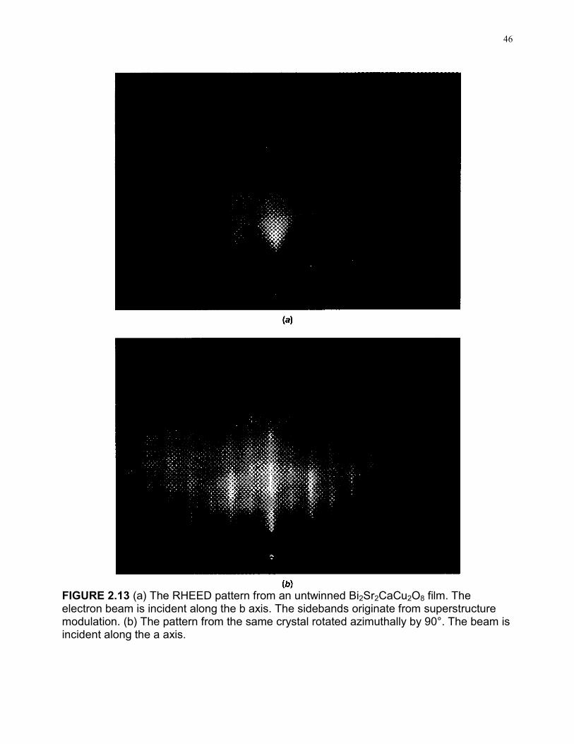
FIGURE 2.14 The RHEED pattern from a twinned Bi2Sr2CaCu2O8 film. The electron beamis incident along the (110) direction of the SrTiO3 substrate.
substrate (which is cubic). Consequently, bulk Bi2Sr2CaCu2O8 crystals most frequentlyshow extensive twinning between domains oriented along the a and b axes. In twinnedfilms, one observes sidebands like those shown in Figure 2.13a, in both (100) and (010)orientations.
In Figure 2.14, we show a RHEED pattern from a twinned thin film of Bi2Sr2CaCu2O8,taken with the beam along (100). The pattern taken along the (010) direction in this filmwas essentially the same. Notice how strongly this contrasts with our previous exampleillustrated in Figure 2.1 3a and b, where the Bi2Sr2CaCu2O8 film was completelyuntwinned, that is, single domain. In Figure 2.15, we show a cross-sectional TEM image ofa twinned Bi2Sr2CaCu2O8 film. The superstructure modulation is clearly visible, as is a twinboundary near the middle of the picture.Hence, RHEED patterns enable one to easily and unambiguously detect whether a film istwinned or not. In some experiments on Bi2Sr2CaCu2O8 films, twinning is importantbecause certain physical properties (electrical conductivity, reflectance, and otherelectronic properties) are affected by the Bimodulation –they are rather different along thea and b directions. Guided by RHEED, we were able to show that untwinned films can be
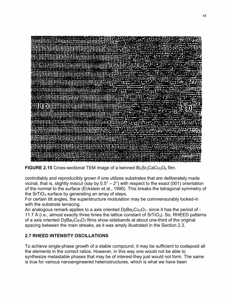
48
FIGURE 2.15 Cross-sectional TEM image of a twinned Bi2Sr2CaCu2O8 film.
controllably and reproducibly grown if one utilizes substrates that are deliberately madevicinal, that is, slightly miscut (say by 0.5° – 2°) with respect to the exact (001) orientationof the normal to the surface (Eckstein et al., 1990). This breaks the tetragonal symmetry ofthe SrTiO3 surface by generating an array of steps.For certain tilt angles, the superstructure modulation may be commensurably locked-inwith the substrate terracing.An analogous remark applies to a axis oriented DyBa2Cu3O7, since it has the period of -11.7 Å (i.e., almost exactly three times the lattice constant of SrTiO3). So, RHEED patternsof a axis oriented DyBa2Cu3O7 films show sidebands at about one-third of the originalspacing between the main streaks, as it was amply illustrated in the Section 2.3.
2.7 RHEED INTENSITY OSCILLATIONS
To achieve single-phase growth of a stable compound, it may be sufficient to codeposit allthe elements in the correct ratios. However, in this way one would not be able tosynthesize metastable phases that may be of interest-they just would not form. The sameis true for various nanoengineered heterostructures, which is what we have been
49
interested in the first place. Hence, we have been trying deliberately to achieve film growththat is substantially kinetically controlled. This implies that apart from p, T, and the
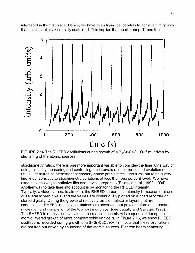
FIGURE 2.16 The RHEED oscillations during growth of a Bi2Sr2CaCu2O8 film, driven byshuttering of the atomic sources.
stoichiometry ratios, there is one more important variable to consider-the time. One way ofdoing this is by measuring and controlling the intervals of occurrence and evolution ofRHEED features of intermittent secondary-phase precipitates. This turns out to be a veryfine knob, sensitive to stoichiometry variations at less than one percent level. We haveused it extensively to optimize film and device properties (Eckstein et al., 1992, 1994).Another way to take time into account is by monitoring the RHEED intensity.Typically, a video camera is aimed at the RHEED screen, the intensity is measured at oneor several screen pixels, and the values are continuously plotted on a chart recorder orstored digitally. During the growth of relatively simple molecular layers that arecodeposited, RHEED intensity oscillations are observed that provide information aboutnucleation and completion of the topmost monolayer (see Lagally and Savage, 1993).The RHEED intensity also evolves as the reaction chemistry is sequenced during theatomic layered growth of more complex oxide unit cells. In Figure 2.16, we show RHEEDoscillations recorded during growth of a Bi2Sr2CaCu2O8 film. Note that these oscillationsare not free but driven by shuttering of the atomic sources. Electron beam scattering
50
depends on the atomic number of the surface atoms, and hence periodic changes of thecomposition of the surface layer induce periodic changes in the intensity of RHEEDstreaks.
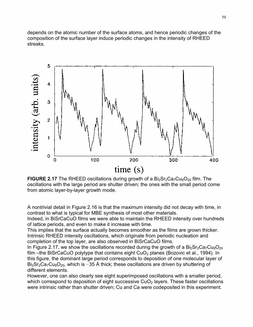
FIGURE 2.17 The RHEED oscillations during growth of a Bi2Sr2Ca7Cu8O20 film. Theoscillations with the large period are shutter driven; the ones with the small period comefrom atomic layer-by-layer growth mode.
A nontrivial detail in Figure 2.16 is that the maximum intensity did not decay with time, incontrast to what is typical for MBE synthesis of most other materials.Indeed, in BiSrCaCuO films we were able to maintain the RHEED intensity over hundredsof lattice periods, and even to make it increase with time.This implies that the surface actually becomes smoother as the films are grown thicker.Intrinsic RHEED intensity oscillations, which originate from periodic nucleation andcompletion of the top layer, are also observed in BiSrCaCuO films.In Figure 2.17, we show the oscillations recorded during the growth of a Bi2Sr2Ca7Cu8O20film –the BiSrCaCuO polytype that contains eight CuO2 planes (Bozovic et al., 1994). Inthis figure, the dominant large period corresponds to deposition of one molecular layer ofBi2Sr2Ca7Cu8O20, which is J35 Å thick; these oscillations are driven by shuttering ofdifferent elements.However, one can also clearly see eight superimposed oscillations with a smaller period,which correspond to deposition of eight successive CuO2 layers. These faster oscillationswere intrinsic rather than shutter driven; Cu and Ca were codeposited in this experiment.
51
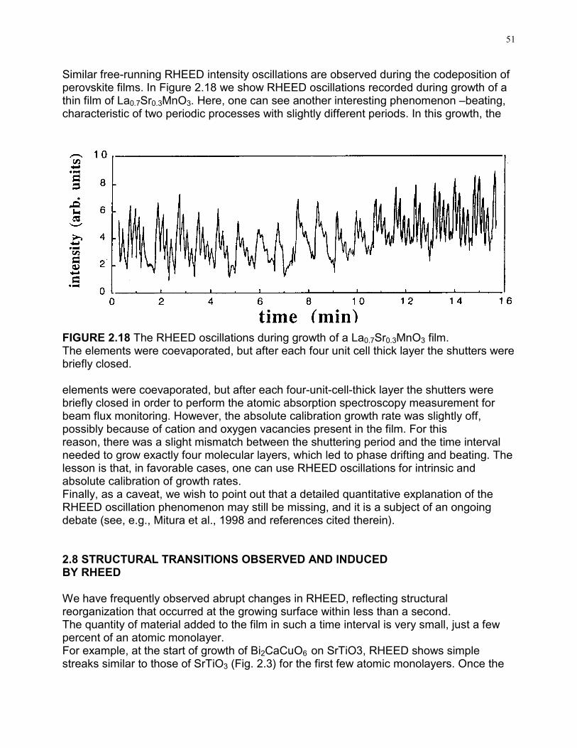
Similar free-running RHEED intensity oscillations are observed during the codeposition ofperovskite films. In Figure 2.18 we show RHEED oscillations recorded during growth of athin film of La0.7Sr0.3MnO3. Here, one can see another interesting phenomenon –beating,characteristic of two periodic processes with slightly different periods. In this growth, the
FIGURE 2.18 The RHEED oscillations during growth of a La0.7Sr0.3MnO3 film.The elements were coevaporated, but after each four unit cell thick layer the shutters werebriefly closed.
elements were coevaporated, but after each four-unit-cell-thick layer the shutters werebriefly closed in order to perform the atomic absorption spectroscopy measurement forbeam flux monitoring. However, the absolute calibration growth rate was slightly off,possibly because of cation and oxygen vacancies present in the film. For thisreason, there was a slight mismatch between the shuttering period and the time intervalneeded to grow exactly four molecular layers, which led to phase drifting and beating. Thelesson is that, in favorable cases, one can use RHEED oscillations for intrinsic andabsolute calibration of growth rates.Finally, as a caveat, we wish to point out that a detailed quantitative explanation of theRHEED oscillation phenomenon may still be missing, and it is a subject of an ongoingdebate (see, e.g., Mitura et al., 1998 and references cited therein).
2.8 STRUCTURAL TRANSITIONS OBSERVED AND INDUCEDBY RHEED
We have frequently observed abrupt changes in RHEED, reflecting structuralreorganization that occurred at the growing surface within less than a second.The quantity of material added to the film in such a time interval is very small, just a fewpercent of an atomic monolayer.For example, at the start of growth of Bi2CaCuO6 on SrTiO3, RHEED shows simplestreaks similar to those of SrTiO3 (Fig. 2.3) for the first few atomic monolayers. Once the
52
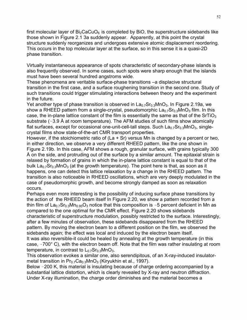
first molecular layer of Bi2CaCuO6 is completed by BiO, the superstructure sidebands likethose shown in Figure 2.1 3a suddenly appear. Apparently, at this point the crystalstructure suddenly reorganizes and undergoes extensive atomic displacement reordering.This occurs in the top molecular layer at the surface, so in this sense it is a quasi-2Dphase transition.
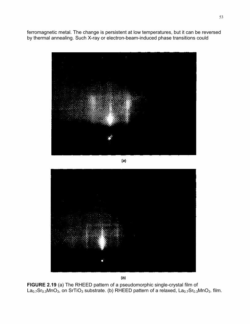
Virtually instantaneous appearance of spots characteristic of secondary-phase islands isalso frequently observed. In some cases, such spots were sharp enough that the islandsmust have been several hundred angstroms wide.These phenomena are veritable surface-phase transitions –a displacive structuraltransition in the first case, and a surface roughening transition in the second one. Study ofsuch transitions could trigger stimulating interactions between theory and the experimentin the future.Yet another type of phase transition is observed in La0.7Sr0.3MnO3. In Figure 2.19a, weshow a RHEED pattern from a single-crystal, pseudomorphic La0.7Sr0.3MnO3 film. In thiscase, the in-plane lattice constant of the film is essentially the same as that of the SrTiO3substrate (J3.9 Å at room temperature). The AFM studies of such films show atomicallyflat surfaces, except for occasional one-unit-cell-tall steps. Such La0.7Sr0.3MnO3, single-crystal films show state-of-the-art CMR transport properties.However, if the stoichiometric ratio of (La + Sr) versus Mn is changed by a percent or two,in either direction, we observe a very different RHEED pattern, like the one shown inFigure 2.19b. In this case, AFM shows a rough, granular surface, with grains typically 300Å on the side, and protruding out of the surface by a similar amount. The epitaxial strain isrelaxed by formation of grains in which the in-plane lattice constant is equal to that of thebulk La0.7Sr0.3MnO3 (at the growth temperature). The point here is that, as soon as ithappens, one can detect this lattice relaxation by a change in the RHEED pattern. Thetransition is also noticeable in RHEED oscillations, which are very deeply modulated in thecase of pseudomorphic growth, and become strongly damped as soon as relaxationoccurs.Perhaps even more interesting is the possibility of inducing surface phase transitions bythe action of the RHEED beam itself In Figure 2.20, we show a pattern recorded from athin film of La0.7Sr0.3Mn0.95O3 notice that this composition is J5 percent deficient in Mn ascompared to the one optimal for the CMR effect. Figure 2.20 shows sidebandscharacteristic of superstructure modulation, possibly restricted to the surface. Interestingly,after a few minutes of observation, these sidebands disappeared from the RHEEDpattern. By moving the electron beam to a different position on the film, we observed thesidebands again; the effect was local and induced by the electron beam itself.It was also reversible-it could be healed by annealing at the growth temperature (in thiscase, J700° C), with the electron beam off. Note that the film was rather insulating at roomtemperature, in contrast to L0.7Sr0.3MnO3.This observation evokes a similar one, also serendipitous, of an X-ray-induced insulator-metal transition in Pr0.7Ca0.3MnO3 (Kiryukhin et al., 1997).Below J200 K, this material is insulating because of charge ordering accompanied by asubstantial lattice distortion, which is clearly revealed by X-ray and neutron diffraction.Under X-ray illumination, the charge order diminishes and the material becomes a
53
ferromagnetic metal. The change is persistent at low temperatures, but it can be reversedby thermal annealing. Such X-ray or electron-beam-induced phase transitions could
FIGURE 2.19 (a) The RHEED pattern of a pseudomorphic single-crystal film ofLa0.7Sr0.3MnO3, on SrTiO3 substrate. (b) RHEED pattern of a relaxed, La0.7Sr0.3MnO3. film.
54
FIGURE 2.20 The RHEED pattern of a La0.7Sr0.3Mn0.95O3 film, at Ts = 700° C, showingsuperstructure modulation.
attract more attention in the future, in the quest for both fundamental insights and for all-solid-state, high-resolution particle and radiation detectors and imaging arrays.
2.9 BEYOND THE PRESENT RHEED ANALYSIS
In recent years, a number of groups have been trying to further improve or expand therange of in situ, real-time RHEED diagnostics. For example, several groups havesuccessfully implemented RHEED in pulsed laser deposition PLD) systems. Note that inthe case of cuprates, PLD is usually performed under relatively high oxygen pressure (ofthe order of 0.1 Torr), enough to burn hot filaments. Solutions to this problem include apulsed oxygen source that is opened only briefly and concurrently with laser firing (Chernet al., 1992), differential pumping on the RHEED manifold (Rijnders et al., 1997), andutilization of reactive gases such as NO2 or O3 (Koinuma et al., 1991; Tabata et al., 1989;Matsumoto et al., 1991).Next, researchers have been looking for ways to extract more information, for example, byrecording and reanalyzing RHEED video movies of each growth (Lagües, 1994), or bysubtracting steady background recorded when the surface is the flattest from subsequentimages (Bodin et al., 1992). "Stroboscopic" real-time RHEED monitoring of rotatingsubstrates (Matijasevic, 1997) is yet another interesting new implementation. Finally, therehave been attempts to supplement RHEED by other analytical techniques, such as the

55
Auger electron spectroscopy (AES) or X-ray absorption spectroscopy. Since the electronscome from the RHEED gun with a substantial kinetic energy, in some configurations ashigh as 35 keV, they can generate a range of excitations in the target material. Variousdeexcitation channels are also possible, and one could select one or more of these tomonitor. These inelastic processes can be detected and examined in parallel to andwithout disrupting the observation of the elastically reflected (and diffracted) electronbeam.Particularly attractive here is the possibility to obtain chemical information. Indeed, onecould benefit a lot from the ability to monitor the elemental composition of the surface, andin particular at the topmost atomic layer. A way to accomplish this is by both exciting anddetecting at a grazing angle. Examples of such instrumentation are the RHEED/TRAXS(total reflection angle X-ray spectroscopy) apparatus at ISTEC in Tokyo, Japan (Kamei etal., 1992, 1993), and the RHEED/AES (Auger electron spectroscopy) system at theElectrotechnical Laboratory in Tsukuba, Japan (Nonaka et al., 1993 a,b).These efforts are still in the pioneering stage, awaiting commercial production and broaderutilization.
2.10 CONCLUSIONS AND OUTLOOK
In recent years, there has been a surge of interest in deposition of high-quality (i.e.,single-crystal) films of complex oxides such as cuprate superconductors or perovskiteferroelectrics. The RHEED method is currently one of the important technique for in situ,real-time analysis of the growing surface of such films.Here, we have reviewed some less well-known issues specific to RHEED monitoring ofdeposition of complex oxides. These include observations of superstructure modulationand twinning, a study of the evolution of long-range order during the growth of thin films ofa axis oriented DyBa2Cu3O7-x as a function of atomic mobility on the surface, and adiscovery of surface phase transitions induced by the electron beam.The RHEED analysis can be made quantitative. We have illustrated this by performingsome numerical simulations and comparing the calculated RHEED patterns to theexperimentally observed ones. In the future, one could expect that real-time RHEEDanalysis can and will be perfected further. For example, one could expect that intelligentprograms will be developed, including pattern recognition capability based on a builtinlibrary of RHEED images, to aid the grower and ultimately even to control the growth.
ACKNOWLEDGMENTS
The authors would like to thank many colleagues for stimulating conversations during thetime this work was done. We also thank the Office of Naval Research, the Naval ResearchLaboratory, and the National Science Foundation for their support of this work, and to theMaterials Research Society for permission to use material from Bozovic and Eckstein,1995 and Bozovic et al., 1997.
56
REFERENCES
Barner, J.B., Rogers, C. T., Inam, A., Ramesh, R., and Bersey, S., Appl. Phys. Lett., 59,472 (1991).
Bodin, P., Sakai, S., and Kasai, Y. Jpn. J. Appl. Phys. Lett., 31 949 (1992).Borman, R. and Nölting, J. Appl. Phys. Lett., 54, 2148 (1989).Bozovic, I. and Eckstein, J. N. MRS Bull., 20(5), 32 (1995).Bozovic, I., Eckstein, J. N., Bozovic, N., and O'Donnell, J., in In Situ Process Diagnostics
and Intelligent Materials Processing, edited by P. A. Rosenthal, W. M. Duncan,and J. A. Woolam, Mat. Res. Soc. Symp. Proc.. 169, 503 (1997).
Bozovic, I., Eckstein, J. N., and Virshup, C. F., Physica C 235-240, 178 (1994).Chaiken, A., Wall, M. A., Howell, R. H., et al. J. Mater Res., 11, 1609 (1996).Chern, M. Y, Gupta, A., and Hussey, B. W. Appl.. Phys. Lett., 60, 3045 (1992).Eckstein, J. N., Bozovic, I., Klausmeier-Brown, M. E., Virshup, C., and Ralls, K. S.,
MRS Bull., 17(8), 27 (1992).Eckstein, J. N., Bozovic, I., Schlom, D. C., and Hats, J. S., Jr., Appl. Phys. Lett. 57,
1049 (1990).Eckstein, J. N., Bozovic, I., and Virshup, C. K, MRS Bull., 19(9), 44 (1994).Eom, C. B., Marshall, A. F, Laderman, S. S., Jacowitz, R. D., and Geballe, T. H.,
Science, 249, 1549 1990.Eom, C. B., Marshall, A. F., Triscone, J. M. et al. Science, 251, 780 (1991).Hashimoto, T., Sagoi, M., Mizutani, Y, Yoshida, J., and Mizushima, K., Appl. Phys.
Lett., 60, 1756 (1992).Jin, S., McCormack, M., Tiefel, T. H., and Ramesh, R., J. Appl. Phys., 76, 6929
(1994).Kamei, M., Aoki, Y, Usui, T., and Morishita, T., Jpn. J. Appl. Phys., 31, 1326 (1992).Kamei, M., Aoki, Y, Ogota, S., Usui, T., and Morishita, T., J. Appl. Phys., 74, 436
(1993).Kiryukhin, V., Casa D., and Hill, J. P. et al. Science, 386, 813 (1997).Koinuma, H., Nagata, H., Tsukahara, T., Gonda, S., and Yoshimoto, M., Appl. Phys.
Lett., 58, 2027 (1991).Lagally, M., in Methods of Experimental Physics 22, 237 (Academic Press, NY,
1985).Lagally, M. C. and Savage, D. B., MRS Bull., 18(1), 24 (1993).Lagües, M., private communication (1994).Matijasevic, V., Rosenthal, F, Shinohara, K. et al. J. Mater. Res., 6, 682 (1991).Matijasevic, V., private communication (1997).Matsumoto, T., Kawai, T., Kitahama, K., et al. (1991) Appl. Phys. Lett., 58, 2039
(1991).Mitura, Z., Dudarev, S. L., and Whelan, M. J., Phys. Rev. B, 57, 6309 (1998).Nonaka, H., Shimizu, T., and Arai, K., Physica C, 217, 280 (1993a).Nonaka, H., Shimizu, T., Ichimura, S., and Arai, K., J. Vac. Sci. Technol. A, 11, 2676
(1993b).
57
Rijnders, G. J. H. M., Koster, G., Blank, D. H. A., and Rogalla, H., Appl. Phys. Lett.,70, 1888 (1997).
Suzuki, Y., Lew, D., Marshall, A. F., Beasley, M. R., and Geballe, T. H., Phys. Rev. B,48, 10642 (1993).
Suzuki, Y., Triscone, J.-M., Eom, C. B., Beasley, M. R., and Geballe, T. H., Phys. Rev.Lett., 73, 328 (1994).
Tabata, H., Kawai, I., Kanai, M., Murata, 0., and Kawai, S., Jpn. J. Appl. Phys. Lett.28, 823 (1989).
Takahashi, H., Izumi, H., Ohata, K. et al., Physica C, 179, 291 (1991).Takahashi, H., Ohata, K., and Morishita, T., Physica C, 201, 273 (1992).Umezawa, I., Lew, D. J., Streiffer, S. K., and Beasley, M. R., Appl. Phys. Lett., 63,
3221 (1993).