RECTIFIER CIRCUITS - phy.uniri.hr · The difference between output and input voltage will be only...
13
RECTIFIER CIRCUITS Semiconductor diode is the basic element of the rectifying circuit due to its rectifying properties. Diode forwards the current only in one direction, and blocks in the opposite, which allows it to rectify alternate current (AC) and voltage into direct current (DC) and voltage. So, diode has low resistance in one direction of the current, and very large in the opposite. Ideal diode will have zero resistance in forward direction, and infinite in the reverse direction. This is one of the most important applications of the diode in electronic circuits. Rectifying circuits are essential in all modern electronics, appliances and instruments that use city power supply in order to rectify AC voltage into constant DC voltage with no fluctuations. Stable voltage and stable power supply is extremely important in many sensitive modern instruments and equipment. CAPACITOR Capacitor is an electronic element that stores electric charge. In a simple approximation, it can be considered to consist of two parallel equal metal plates that can store electric charge. In order to preserve electric neutrality, plates must store opposite charges and the electric field between the plates arises. Energy of the electric field is also stored in the capacitor. Capacitance C of a capacitor represents amount of electric charge dQ stored on the plates of the capacitor per difference of electric potential (voltage) dU between the plates: = In other words, capacitance is change in the electric charge stored in the capacitor per the change in its electric potential. Capacitance of a plate capacitor made of two equal parallel plates with the surface area S spaced at a distance d: = 0 where 0 = 8.854 · 10 -12 F/m is dielectric constant of the vacuum or vacuum permittivity; r is dielectric constant or permittivity of the material that fills the space between the plates (if vacuum fills the space, r = 1).
-
Upload
vuongthuan -
Category
Documents
-
view
230 -
download
0
Transcript of RECTIFIER CIRCUITS - phy.uniri.hr · The difference between output and input voltage will be only...

RECTIFIER CIRCUITS
Semiconductor diode is the basic element of the rectifying circuit due to its rectifying properties. Diode forwards the current only in one direction, and blocks in the opposite, which allows it to rectify alternate current (AC) and voltage into direct current (DC) and voltage. So, diode has low resistance in one direction of the current, and very large in the opposite. Ideal diode will have zero resistance in forward direction, and infinite in the reverse direction. This is one of the most important applications of the diode in electronic circuits. Rectifying circuits are essential in all modern electronics, appliances and instruments that use city power supply in order to rectify AC voltage into constant DC voltage with no fluctuations. Stable voltage and stable power supply is extremely important in many sensitive modern instruments and equipment.
CAPACITOR
Capacitor is an electronic element that stores electric charge. In a simple
approximation, it can be considered to consist of two parallel equal metal plates that
can store electric charge. In order to preserve electric neutrality, plates must store
opposite charges and the electric field between the plates arises. Energy of the electric
field is also stored in the capacitor. Capacitance C of a capacitor represents amount of
electric charge dQ stored on the plates of the capacitor per difference of electric
potential (voltage) dU between the plates:
𝐶 =𝑑𝑄
𝑑𝑈
In other words, capacitance is change in the electric charge stored in the capacitor per
the change in its electric potential.
Capacitance of a plate capacitor made of two equal parallel plates with the
surface area S spaced at a distance d:
𝐶 = 0𝑟
𝑆
𝑑
where 0 = 8.854 · 10-12 F/m is dielectric constant of the vacuum or vacuum permittivity;
r is dielectric constant or permittivity of the material that fills the space between the
plates (if vacuum fills the space, r = 1).
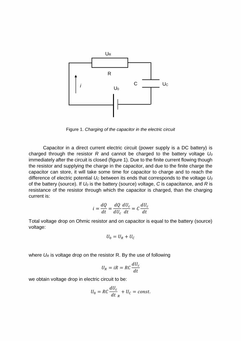
Figure 1. Charging of the capacitor in the electric circuit
Capacitor in a direct current electric circuit (power supply is a DC battery) is
charged through the resistor R and cannot be charged to the battery voltage U0
immediately after the circuit is closed (figure 1). Due to the finite current flowing though
the resistor and supplying the charge in the capacitor, and due to the finite charge the
capacitor can store, it will take some time for capacitor to charge and to reach the
difference of electric potential UC between its ends that corresponds to the voltage U0
of the battery (source). If U0 is the battery (source) voltage, C is capacitance, and R is
resistance of the resistor through which the capacitor is charged, than the charging
current is:
𝑖 =𝑑𝑄
𝑑𝑡=
𝑑𝑄
𝑑𝑈𝑐
𝑑𝑈𝑐
𝑑𝑡= 𝐶
𝑑𝑈𝑐
𝑑𝑡
Total voltage drop on Ohmic resistor and on capacitor is equal to the battery (source)
voltage:
𝑈0 = 𝑈𝑅 + 𝑈𝐶
where UR is voltage drop on the resistor R. By the use of following
𝑈𝑅 = 𝑖𝑅 = 𝑅𝐶𝑑𝑈𝑐
𝑑𝑡
we obtain voltage drop in electric circuit to be:
𝑈0 = 𝑅𝐶𝑑𝑈𝑐
𝑑𝑡 𝑅+ 𝑈𝐶 = 𝑐𝑜𝑛𝑠𝑡.
U0
UC C
R
i
UR
The above equation represents differential equation of voltage drop on capacitor.
Solution of this differential equation has the form:
𝑈𝐶 = 𝐴𝑒−𝑝𝑡 + 𝐵
where coefficients A and B can be determined from boundary conditions at the
beginning (t=0) of the charging of the capacitor:
𝑈𝐶(𝑡 = 0) = 0 𝑉
while the voltage drop on capacitor after very long time (t→) must become equal to
the battery (source) voltage:
𝑈𝐶(𝑡 → ∞) = 𝑈0
Finally, voltage drop on capacitor is:
𝑈𝐶 = 𝑈0(1 − 𝑒−𝑡/𝑅𝐶) = 𝑈0(1 − 𝑒−𝑡/𝜏)
where = RC is the characteristic charging time of the capacitor.
According to the above equation, capacitor cannot be charged instantly to the battery (source) voltage, and this process takes some time which is characterized by
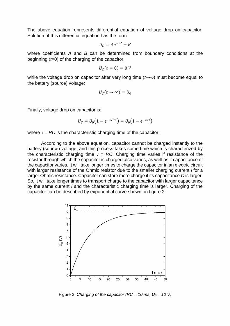
the characteristic charging time = RC. Charging time varies if resistance of the resistor through which the capacitor is charged also varies, as well as if capacitance of the capacitor varies. It will take longer times to charge the capacitor in an electric circuit with larger resistance of the Ohmic resistor due to the smaller charging current i for a larger Ohmic resistance. Capacitor can store more charge if its capacitance C is larger. So, it will take longer times to transport charge to the capacitor with larger capacitance by the same current i and the characteristic charging time is larger. Charging of the capacitor can be described by exponential curve shown on figure 2.
Figure 2. Charging of the capacitor (RC = 10 ms, U0 = 10 V)

Capacitor discharging it equivalent to the charging process. It will take finite time to carry away all the charge stored in the capacitor and to drop the voltage across the capacitor to zero if the capacitor is discharged through the resistor R. Discharging is also described by exponential drop of the voltage across the capacitor in time:
𝑈𝐶 = 𝑈0𝑒−𝑡/𝑅𝐶 = 𝑈0𝑒−𝑡/𝜏
Again, characteristic discharging time of the capacitor is = RC. Equivalently, discharge will be faster if the discharging current is larger and the Ohmic resistance through which the capacitor is discharged smaller. Discharge time will be shorter if smaller amount of charge is stored in the capacitor, i.e. if the capacitance C of the capacitor is smaller.
Figure 3. Discharging of the capacitor (RC = 10 ms, U0 = 10 V)
HALF-WAVE RECTIFIER CIRCUIT
Half-wave rectifier is the simples rectifying circuit. The circuit, as well as the shapes of the input AC voltage and output DC voltage are shown on figures 4a and 4b. Diode is forward biased and the current can flow though it and through the load resistor (Rp) during the positive half-period of the input AC voltage. Voltage drop on the load resistor will be proportional to the current and have the same shape as the input AC voltage. The difference between output and input voltage will be only due to the small voltage drop on the diode UD (diode resistance in the forward bias direction
is small but still finite). Diode is reverse biased during negative half-period of the input voltage and only the reverse bias current is flowing through the diode. Reverse bias
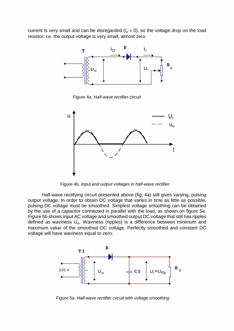
current is very small and can be disregarded (Is 0), so the voltage drop on the load
resistor, i.e. the output voltage is very small, almost zero.
iD i i
u uU i
p
Figure 4a. Half-wave rectifier circuit
uu
Ui u
Figure 4b. Input and output voltages in half-wave rectifier
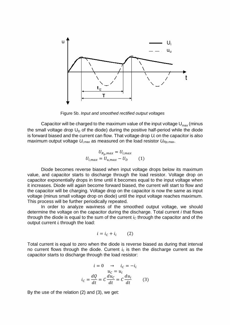
Half-wave rectifying circuit presented above (fig. 4a) still gives varying, pulsing
output voltage. In order to obtain DC voltage that varies in time as little as possible, pulsing DC voltage must be smoothed. Simplest voltage smoothing can be obtained by the use of a capacitor connected in parallel with the load, as shown on figure 5a. Figure 5b shows input AC voltage and smoothed output DC voltage that still has ripples defined as waviness Uw. Waviness (ripples) is a difference between minimum and
maximum value of the smoothed DC voltage. Perfectly smoothed and constant DC voltage will have waviness equal to zero.
p220 V u u U i=URp
Figure 5a. Half-wave rectifier circuit with voltage smoothing
u Ui
uu
Figure 5b. Input and smoothed rectified output voltages
Capacitor will be charged to the maximum value of the input voltage Umax (minus
the small voltage drop UD of the diode) during the positive half-period while the diode
is forward biased and the current can flow. That voltage drop Ui on the capacitor is also maximum output voltage Ui,max as measured on the load resistor URp,max.
𝑈𝑅𝑝,𝑚𝑎𝑥 = 𝑈𝑖,𝑚𝑎𝑥
𝑈𝑖,𝑚𝑎𝑥 = 𝑈𝑢,𝑚𝑎𝑥 − 𝑈𝐷 (1)
Diode becomes reverse biased when input voltage drops below its maximum
value, and capacitor starts to discharge through the load resistor. Voltage drop on capacitor exponentially drops in time until it becomes equal to the input voltage when it increases. Diode will again become forward biased, the current will start to flow and the capacitor will be charging. Voltage drop on the capacitor is now the same as input voltage (minus small voltage drop on diode) until the input voltage reaches maximum. This process will be further periodically repeated.
In order to analyze waviness of the smoothed output voltage, we should determine the voltage on the capacitor during the discharge. Total current i that flows through the diode is equal to the sum of the current iC through the capacitor and of the output current ii through the load:
𝑖 = 𝑖𝐶 + 𝑖𝑖 (2)
Total current is equal to zero when the diode is reverse biased as during that interval no current flows through the diode. Current ic is then the discharge current as the capacitor starts to discharge through the load resistor:
𝑖 = 0 → 𝑖𝐶 = −𝑖𝑖
𝑢𝐶 = 𝑢𝑖
𝑖𝐶 =𝑑𝑄
𝑑𝑡= 𝐶
𝑑𝑢𝐶
𝑑𝑡= 𝐶
𝑑𝑢𝑖
𝑑𝑡 (3)
By the use of the relation (2) and (3), we get:
𝑖𝑖 = −𝐶𝑑𝑢𝑖
𝑑𝑡=
𝑢𝑖
𝑅𝑝 (4)
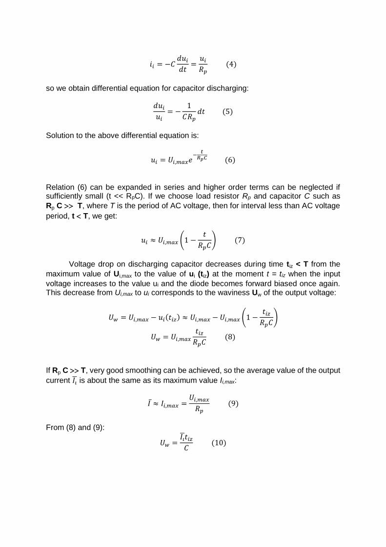
so we obtain differential equation for capacitor discharging:
𝑑𝑢𝑖
𝑢𝑖= −
1
𝐶𝑅𝑝𝑑𝑡 (5)
Solution to the above differential equation is:
𝑢𝑖 = 𝑈𝑖,𝑚𝑎𝑥𝑒−
𝑡𝑅𝑝𝐶 (6)
Relation (6) can be expanded in series and higher order terms can be neglected if sufficiently small (t << RpC). If we choose load resistor Rp and capacitor C such as
Rp C T, where T is the period of AC voltage, then for interval less than AC voltage
period, t T, we get:
𝑢𝑖 ≈ 𝑈𝑖,𝑚𝑎𝑥 (1 −𝑡
𝑅𝑝𝐶) (7)
Voltage drop on discharging capacitor decreases during time tiz < T from the
maximum value of Ui,max to the value of ui (tiz) at the moment t = tiz when the input
voltage increases to the value ui and the diode becomes forward biased once again. This decrease from Ui,max to ui corresponds to the waviness Uw of the output voltage:
𝑈𝑤 = 𝑈𝑖,𝑚𝑎𝑥 − 𝑢𝑖(𝑡𝑖𝑧) ≈ 𝑈𝑖,𝑚𝑎𝑥 − 𝑈𝑖,𝑚𝑎𝑥 (1 −𝑡𝑖𝑧
𝑅𝑝𝐶)
𝑈𝑤 = 𝑈𝑖,𝑚𝑎𝑥
𝑡𝑖𝑧
𝑅𝑝𝐶 (8)
If Rp C T, very good smoothing can be achieved, so the average value of the output
current 𝐼�̅� is about the same as its maximum value Ii,max:
𝐼 ̅ ≈ 𝐼𝑖,𝑚𝑎𝑥 =𝑈𝑖,𝑚𝑎𝑥
𝑅𝑝 (9)
From (8) and (9):
𝑈𝑤 =𝐼�̅�𝑡𝑖𝑧
𝐶 (10)

FULL-WAVE RECTIFIER CIRCUIT (using center-tapped transformer)
Full-wave rectifier circuit is shown in figure 6a. This electric circuit provide higher DC currents and lower waviness of the output rectified voltage than the half-wave rectifier circuit. This is achieved by the use of both half-periods of the AC input voltage in order to obtain DC voltage. In half-wave rectifier circuit, only one half-period (positive) of the input voltage is used for rectifying. Full-wave rectifier circuit in figure 6a uses center-tapped transformer, a connection at the middle of the secondary winding of the transformer. So, half of the input voltage on secondary winding of the transformer is used for rectification in every half-period of the input AC voltage. Diode D1 is forward biased and D2 is reverse biased, and the current flows through the diode D1 and load resistor in the positive half-period of the input AC voltage. This current causes positive voltage drop on the load, which corresponds to the output voltage. Diode D1 becomes reverse biased and diode D2 forward biased during the negative half-period of the input AC voltage. Current flows through the diode D2 and load resistor which is connected to the lower half of the secondary winding. Direction of the current and polarity of the voltage on the load resistor remain the same as before and during the positive half-period. Rectified pulsating DC voltage is obtained with the frequency twice the value of the frequency of the input AC signal. This pulsating rectified voltage must be smoothed in order to obtain constant DC voltage. Smoothing is achieved as in half-wave rectifier by the use of capacitor in parallel with the load resistor. Capacitor will be charged twice during one period of the input DC signal in the full-wave rectifier. This reduces waviness for around two times compared to half-wave rectifier. Both diodes take part in rectifying, each in one half-period, so average value of the output
current 𝐼 ̅is twice the average value of the current 𝐼�̅� in each of two diodes:
𝐼 ̅ = 2𝐼�̅�
u u
u u
I i
u i
Figure 6a. Half-wave rectifier circuit

Ui izglađeni
Uu
U ispravljeni pulzirajući
u
t
Figure 6b. Input AC voltage, pulsating rectified DC voltage and smoothed
rectified DC output voltage
VOLTAGE STABILIZER
Zener diode is most commonly used to stabilize the voltage. Zener diode works in reverse bias when electric breakthrough occurs. I-U characteristics of working regime of the Zener diode is shown on figure 7b, while the corresponding electric circuit with Zener diode is shown on figure 7a.
Rp
Figure 7a. Voltage stabilizer with Zener diode
Izmin
Iz
Izmax
UpUzUzmax
Figure 7b. I-U characteristics of the Zener diode
Smoothed rectified
output DC voltage
Pulsating rectified
DC voltage

Currents though the Zener diode can vary in very broad range from minimal Iz,min to maximal Iz,max values. Minimal value of the current through the reverse biased Zener diode is determined by the breakthrough voltage Up. Voltage is not stabilized below the breakthrough voltage. Zener diode is overloaded if the voltage reaches the value of Uz,max with the current Iz,max.
Stability of the output voltage depends on: a) variations of the input voltage b) variations of the output current
a) Assume that the resistance Rp of the load resistor is very large, much larger
than the resistance rZ of the Zener diode ( Rp >> rz). In that case, current through the
load is much smaller than the current through the Zener diode, Ip << Iz, so all the
variations of the input current goes through the Zener diode and not through the load.
∆𝐼 ≈ ∆𝐼𝑍 =∆𝑈𝑍
𝑟𝑍 (11)
Total variation of the input voltage U is divided between resistor R (UR) and
Zener diode (UZ):
∆𝑈 = ∆𝑈𝑅 + ∆𝑈𝑍 = (𝑅 + 𝑟𝑍)∆𝐼 (12)
From (11) and (12):
∆𝑈𝑍
∆𝑈=
𝑟𝑍
𝑅 + 𝑟𝑍≈
𝑟𝑍
𝑅≪ 1 (13)
Variation of the voltage on output, which corresponds to the variation of the
voltage drop on Zener diode, is much smaller than the variation of the input voltage.
This ratio is equal to the ratio of the resistance of the Zener diode and resistor R.
Variation of the output voltage can be very small if the resistance of the Zener diode is
also small. Consequently, such an electric circuit acts as a voltage stabilizer.
b) Stabilizer with Zener diode can also stabilize voltage if output current Ip
through the load varies. Assume that the input voltage does not vary, U = 0. Then:
∆𝑈 = ∆𝑈𝑅 + ∆𝑈𝑍 = 0 (14)
Total variation of the current is equal to the sum of the variation of the current that flows though the Zener diode and of the current that flows through the load:
∆𝐼 = ∆𝐼𝑍 + ∆𝐼𝑝 (15)
The current Ip through the load will increase if the load resistance is smaller.
This will cause an increase of the total current I though the resistance R and of the voltage drop on that resistor R. The voltage across the Zener diode must decrease as

the input voltage is constant. So, by increasing the current Ip through the load, voltage drop UZ on Zener diode must decrease and their tendencies are opposite.
Ohm’s law for resistor R and Zener diode:
∆𝐼 =∆𝑈𝑅
𝑅
∆𝐼𝑍 =∆𝑈𝑍
𝑟𝑍
Output current flows through the load, so variation of the output current is – lp and from the above relations and relations (14) and (15) output resistance Ri of the stabilizer can be determined:
𝑅𝑖 =∆𝑈𝑍
−∆𝐼𝑝=
∆𝑈𝑍
∆𝐼𝑍 − ∆𝐼=
∆𝑈𝑍
∆𝑈𝑍
𝑟𝑍−
∆𝑈𝑅
𝑅
=∆𝑈𝑍
∆𝑈𝑍
𝑟𝑍+
∆𝑈𝑍
𝑅
=∆𝑈𝑍
∆𝑈𝑍 (1𝑟𝑍
+1𝑅)
=𝑟𝑍𝑅
𝑟𝑍 + 𝑅
𝑅𝑖 =𝑟𝑍𝑅
𝑟𝑍 + 𝑅=
𝑟𝑍
1 +𝑟𝑍
𝑅
≈ 𝑟𝑍 (16)
So, stabilizer is a voltage source with internal resistance rZ . This resistance rZ
is very small, so the variation of the output voltage is also small.
ASSIGNMENTS: I. Assembly the half-wave rectifier according to the electric circuit scheme, and measure the following:
Uiuu
uu = input AC voltage Ui = output DC voltage
ID = diode current Ii = output current
Rp = load resistor
1. By the use of oscilloscope and without the capacitor C, observe and show the
following on the same diagram: a) Voltage drop across the load resistor without diode connected in the circuit
(Ui = Ui (t)) b) Voltage drop across the load resistor (output voltage) Ui with diode
connected in the circuit c) Voltage drop on diode UD

d) Connect voltages in b) and c) to both channels of the oscilloscope. Compare obtained voltages with the input voltage in order to verify the relation uu = UD + Ui
2. Measure output current Ii vs. diode current ID
a) without capacitor in the circuit b) with capacitor in the circuit (C = 220 F)
3. Measure waviness Uw of the output voltage vs. output current Ii with the constant
capacitance (C = 470 F). Compare results with the expected values obtained by relation (10) on a diagram. Use measured values of the output current Ii and
of the discharging time tiz of the capacitor in relation (10).
4. Measure waviness Uw of the output voltage vs. capacitance of the capacitor C
with constant output current (Ii = 10 mA). Compare the obtained with expected
curve.
5. Measure output voltage Ui vs. input effective voltage Uueff with constant output
current Ii = 0 by the use of the below circuit. Show U f Ui eff ( ) and U Ueff 2
on the same diagram U = f(Ueff). Verify relation 𝑈𝑖 = 𝑈𝑒𝑓𝑓√2 − 𝑈𝐷 by obtaining
UD from the diagram.
uu Ui470 F
II. Assembly the full-wave rectifier according to the electric circuit scheme.
Rp
C = 100, 220, 470, 1000 F Rp = load resistor (potentiometer)
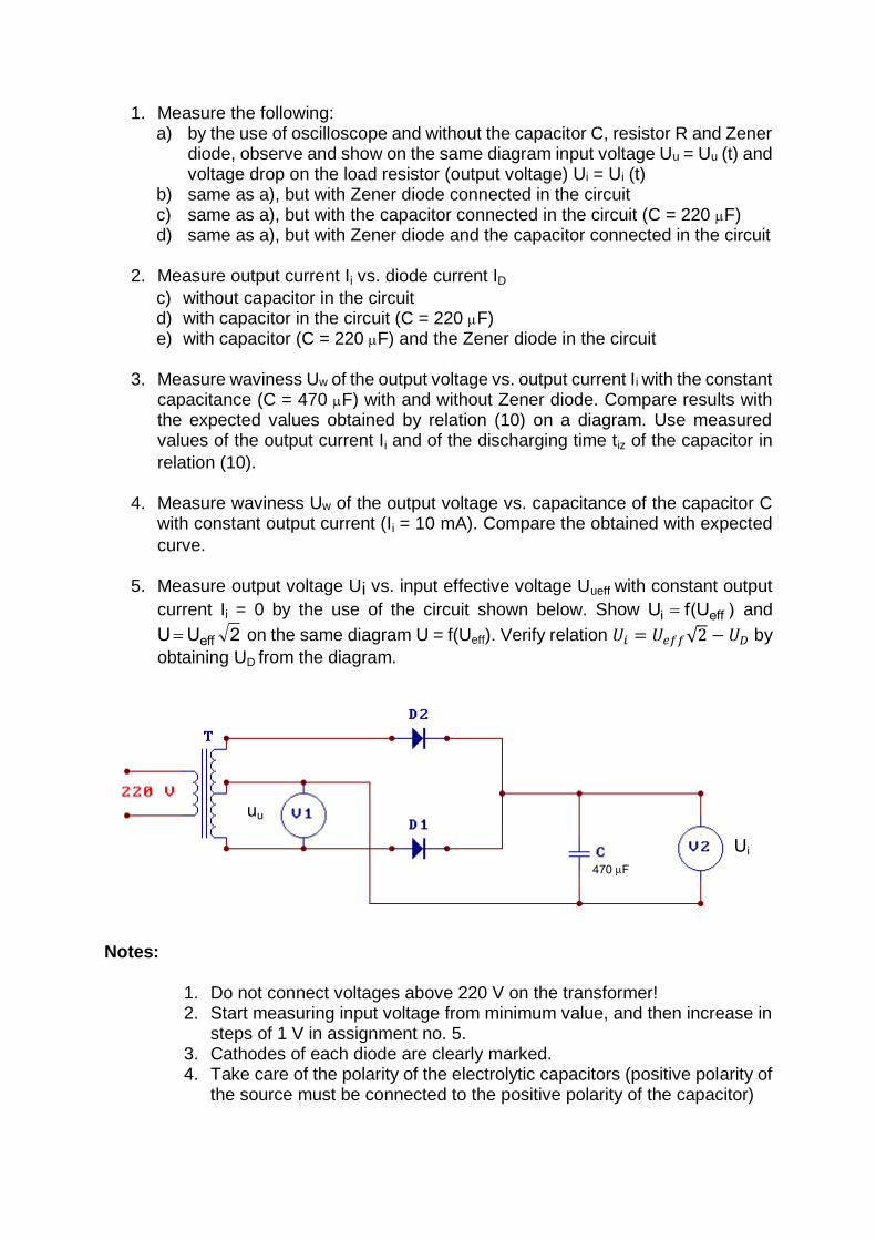
1. Measure the following: a) by the use of oscilloscope and without the capacitor C, resistor R and Zener
diode, observe and show on the same diagram input voltage Uu = Uu (t) and voltage drop on the load resistor (output voltage) Ui = Ui (t)
b) same as a), but with Zener diode connected in the circuit c) same as a), but with the capacitor connected in the circuit (C = 220 F) d) same as a), but with Zener diode and the capacitor connected in the circuit
2. Measure output current Ii vs. diode current ID
c) without capacitor in the circuit d) with capacitor in the circuit (C = 220 F) e) with capacitor (C = 220 F) and the Zener diode in the circuit
3. Measure waviness Uw of the output voltage vs. output current Ii with the constant
capacitance (C = 470 F) with and without Zener diode. Compare results with the expected values obtained by relation (10) on a diagram. Use measured values of the output current Ii and of the discharging time tiz of the capacitor in
relation (10).
4. Measure waviness Uw of the output voltage vs. capacitance of the capacitor C with constant output current (Ii = 10 mA). Compare the obtained with expected
curve.
5. Measure output voltage Ui vs. input effective voltage Uueff with constant output
current Ii = 0 by the use of the circuit shown below. Show U f Ui eff ( ) and
U Ueff 2 on the same diagram U = f(Ueff). Verify relation 𝑈𝑖 = 𝑈𝑒𝑓𝑓√2 − 𝑈𝐷 by
obtaining UD from the diagram.
uu
Ui
470 F
Notes:
1. Do not connect voltages above 220 V on the transformer! 2. Start measuring input voltage from minimum value, and then increase in
steps of 1 V in assignment no. 5. 3. Cathodes of each diode are clearly marked. 4. Take care of the polarity of the electrolytic capacitors (positive polarity of
the source must be connected to the positive polarity of the capacitor)