RECORD OF REVISIONS - chuanling.netchuanling.net/down/LD070WS2-SL02.pdf · RECORD OF REVISIONS 1.0...
26
Product Specification 1 / 26 LD070WS2 Liquid Crystal Display Ver. 1.0 Mar.22, 2011 RECORD OF REVISIONS Final specification - Mar.22, 2011 1.0 Description Page Revision Date Revision No www.DataSheet.co.kr Datasheet pdf - http://www.DataSheet4U.net/
Transcript of RECORD OF REVISIONS - chuanling.netchuanling.net/down/LD070WS2-SL02.pdf · RECORD OF REVISIONS 1.0...

Product Specification
1 / 26
LD070WS2Liquid Crystal Display
Ver. 1.0 Mar.22, 2011
RECORD OF REVISIONS
Final specification-Mar.22, 20111.0
DescriptionPageRevision DateRevision No
www.DataSheet.co.kr
Datasheet pdf - http://www.DataSheet4U.net/

Product Specification
2 / 26
LD070WS2Liquid Crystal Display
Ver. 1.0 Mar.22, 2011
1. General Description
General Features
6-bit + 2-bit FRC, 16,7M colorsColor Depth
1024 horiz. By 600 vert. Pixels RGB strip arrangementPixel Format
400 cd/m2 (Typ.)Luminance, White
95g(Max.)Weight
Transmitting type, normally BlackDisplay Operating Mode
Hard coat on the polarizerSurface Treatment
0.050mm × 0.150mm Dot Pitch
162.8mm x102.9mm x 2.47mm (Typ.)Outline Dimension
7.0 inches diagonal Active Screen Size
The LD070WS2 is a Color Active Matrix Liquid Crystal Display with an integral Light Emitting Diode(LED) backlight system. The matrix employs a-Si Thin Film Transistor as the active element. It is a transmissive type display operating in the normally Black mode. This TFT-LCD has 7.0 inches diagonally measured active display area with WSVGA resolution(1024 horizontal by 600 vertical pixel array). Each pixel is divided into Red, Green and Blue sub-pixels or dots which are arranged in vertical stripes. Gray scale or the brightness of the sub-pixel color is determined with a 6-bit + 2-bit FRC gray scale signal for each dot, thus, presenting a palette of more than 16,772,216 colors.The LD070WS2 has been designed to apply the interface method that enables low power, high speed, low EMI. The LD070WS2 is intended to support applications where thin thickness, low power are critical factors and graphic displays are important. In combination with the vertical arrangement of the sub-pixels, the LD070WS2 characteristics provide an excellent flat display.
CN130pin
SPI
3 Wire
Power circuitblock
Source driverT-con & PWM Embedded
Source driverT-con & PWM Embedded
TFT-LCD Panel(1024×RGB×600 pixels)
TFT-LCD Panel(1024×RGB×600 pixels)
G600
S1024 S1
G1
LED Backlight Ass’yLED Backlight Ass’y
LVDS_CLK
1 Pair
LVDS_DATA
4 Pair
GateDriver
VLED_A
VLED_C
DIMO
DIMI
3 Line
2 Line
8 Line
www.DataSheet.co.kr
Datasheet pdf - http://www.DataSheet4U.net/

Product Specification
3 / 26
LD070WS2Liquid Crystal Display
Ver. 1.0 Mar.22, 2011
2. Absolute Maximum Ratings
The following are maximum values which, if exceeded, may cause faulty operation or damage to the unit.
Table 1. ABSOLUTE MAXIMUM RATINGS
Units
[Note 2-1,2]°C70-20HSTStorage Temperature
[Note 2-1,2,3,4]°C60-10TOPOperating Temperature
at 25 ± 5°CVdc5.0-0.5VCCPower Input Voltage
MaxMinParameter Notes
ValuesSymbol
[Note 2-1] This rating applies to all parts of the module and should not be exceeded.[Note 2-2] Maximum wet-bulb temperature is 46℃. Condensation of dew must be avoided as electrical
current leaks will occur, causing a degradation of performance specifications.[Note 2-3] The operating temperature only guarantees operation of the circuit and doesn’t guarantee
all the contents of Electro-optical specification.[Note 2-4] Ambient temperature when the backlight is lit (reference value).
[Storage range][Storage range][Storage range][Storage range]
[Operation[Operation[Operation[Operation
----20 20 20 20 ----10101010 10101010 20202020 30303030 40404040 50505050 60606060 707070700000
Dry Bulb Temperature [Dry Bulb Temperature [Dry Bulb Temperature [Dry Bulb Temperature [℃℃℃℃]]]]
10101010%%%%
30303030%%%%
60606060%%%%
000010101010
2020202030303030
40404040
50505050
60606060
Wet BulbWet BulbWet BulbWet BulbTemperature [Temperature [Temperature [Temperature [℃℃℃℃]]]]
Hum
idity[(%
)RH
]H
um
idity[(%
)RH
]H
um
idity[(%
)RH
]H
um
idity[(%
)RH
]
80%80%80%80%
www.DataSheet.co.kr
Datasheet pdf - http://www.DataSheet4U.net/
Product Specification
4 / 26
LD070WS2Liquid Crystal Display
Ver. 1.0 Mar.22, 2011
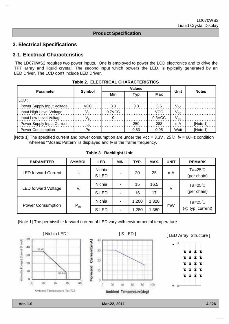
3. Electrical Specifications
3-1. Electrical Characteristics
The LD070WS2 requires two power inputs. One is employed to power the LCD electronics and to drive the TFT array and liquid crystal. The second input which powers the LED, is typically generated by an LED Driver. The LCD don’t include LED Driver.
Table 2. ELECTRICAL CHARACTERISTICS
VDC0.3VCC-0VILInput Low-Level Voltage
VDCVCC-0.7VCCVIHInput High-Level Voltage
[Note 1]Watt0.950.83-PcPower Consumption
VDC3.63.33.0VCCPower Supply Input Voltage
[Note 1]mA288250-ICCPower Supply Input Current
LCD :
Parameter SymbolMaxTypMin
NotesUnitValues
[Note 1] The specified current and power consumption are under the Vcc = 3.3V , 25℃, fv = 60Hz condition whereas “Mosaic Pattern” is displayed and fv is the frame frequency.
Table 3. Backlight Unit
1,3601,280-S-LED
1716-S-LED
-
-
-
MIN.
Ta=25℃
(per chain)mA2520
NichiaS-LED
IfLED forward Current
REMARKUNITMAX.TYP.LEDSYMBOLPARAMETER
Ta=25℃
(@ typ. current)mW
1,3201,200NichiaPBLPower Consumption
Ta=25℃
(per chain)V
16.515NichiaVfLED forward Voltage
[Note 1] The permissible forward current of LED vary with environmental temperature.
[ LED Array Structure ]
+
-
[ Nichia LED ] [ S-LED ]
www.DataSheet.co.kr
Datasheet pdf - http://www.DataSheet4U.net/

Product Specification
5 / 26
LD070WS2Liquid Crystal Display
Ver. 1.0 Mar.22, 2011
3-2. Interface (Input Terminal)
Table 4. Module Connection Pin Configuration(cn1)
This LCD employs one interface connections, a 30 pin connector is used for the module electronics interface.
(Connector Type : 30Pin 0.5mm pitch, Matching Connector : JAE AA01B-S030VA1)
+3.3V Power SupplyVCC
GroundGND
LVDS differential data inputD3-IN-P30
Ground
Backlight Dimmer SignalBL-PWM-OUT29
LVDS differential data inputD3-IN-Nt28
Brightness Control SignalBL-PWM-IN27
GroundGND26
GroundGND25
LVDS differential data inputD2-IN-P24
Serial Communication Data InputSDA23
LVDS differential data inputD2-IN-N22
Serial Communication Clock InputSCL21
GroundGND20
Serial Communication Chip SelectCSB19
LVDS differential data inputD1-IN-P18
No ConnectionNC17
LVDS differential data inputD1-IN-N16
No ConnectionNC15
GroundGND14
GroundGND13
LVDS differential data inputD0-IN-P12
Power Supply For LED [Cathode]LEDN11
LVDS differential data inputD0-IN-N10
Power Supply For LED [Anode]LEDP9
GroundGND8
GND7
LVDS Clock Input (Positive)CLK-IN-P6
+3.3V Power SupplyVCC5
LVDS Clock Input (Negative)CLK-IN-N4
3
2
+3.3V Power SupplyVCC1
NotesDescriptionSymbolNo.
www.DataSheet.co.kr
Datasheet pdf - http://www.DataSheet4U.net/
Product Specification
6 / 26
LD070WS2Liquid Crystal Display
Ver. 1.0 Mar.22, 2011
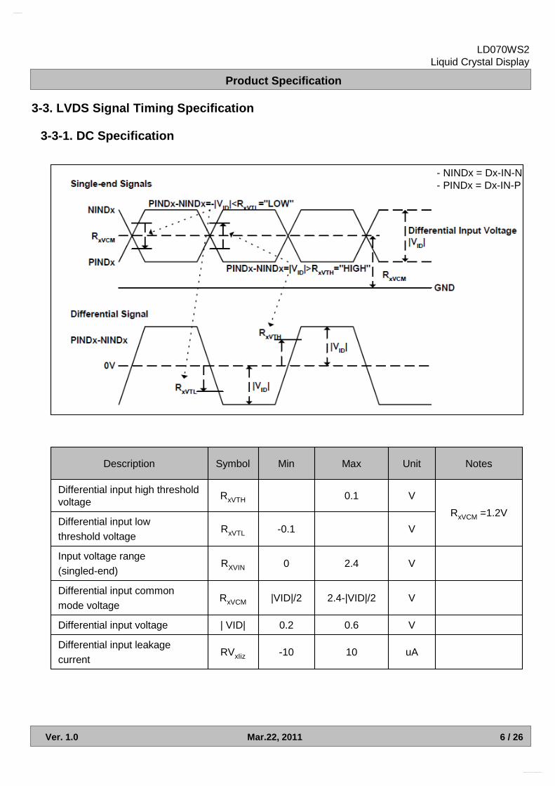
3-3. LVDS Signal Timing Specification
uA10-10RVxIiz
Differential input leakagecurrent
V2.40RXVIN
Input voltage range(singled-end)
V2.4-|VID|/2|VID|/2RxVCM
Differential input commonmode voltage
V0.60.2| VID|Differential input voltage
Description Symbol Min Max Unit Notes
Differential input high threshold voltage
RxVTH 0.1 V
RxVCM =1.2VDifferential input lowthreshold voltage
RxVTL -0.1 V
3-3-1. DC Specification
- NINDx = Dx-IN-N- PINDx = Dx-IN-P
www.DataSheet.co.kr
Datasheet pdf - http://www.DataSheet4U.net/

Product Specification
7 / 26
LD070WS2Liquid Crystal Display
Ver. 1.0 Mar.22, 2011
3-3-2. AC Specification
-
500
45.9
Min
-ns3/(7* RxFCLK)TLVCLClock low time
Description Symbol Typ Max Unit Notes
Clock Frequency RXFCLK - 59.1 MHz
Input Data Skew Margin TRSKM - ps| VID| = 400mVRxVCM = 1.2VRxFCLK = 71 MHz
Clock high time TLVCH 4/(7* RxFCLK) ns -
PLL wake-up time TenPLL 150 us -
PINC= CLK-IN-PNINC= CLK-IN-NINDx = Dx-IN
Ta=25°C, VCC=3.3V
www.DataSheet.co.kr
Datasheet pdf - http://www.DataSheet4U.net/

Product Specification
8 / 26
LD070WS2Liquid Crystal Display
Ver. 1.0 Mar.22, 2011
< LVDS Data Format >
3-3-3. Data Format-. LVDS 1 Port
G0 R5 R4 R3 R2 R1 R0
B1 B0 G5 G4 G3 G2 G1
DE VSYNC HSYNC B5 B4 B3 B2
X B7 B6 G7 G6 R7 R6
R1 R0
G2 G1
B3 B2
R7 R6
G0
B1
DE
X
Current (Nth ) Cycle
R5 R4
B0 G5
VSYNC HSYNC
B7 B6
R3 R2
G4 G3
B5 B4
G7 G6
Previous (N-1)th Cycle Next (N+1)th Cycle
RCLK+
RA+/-
RB+/-
RC+/-
RD+/-
www.DataSheet.co.kr
Datasheet pdf - http://www.DataSheet4U.net/

Product Specification
9 / 26
LD070WS2Liquid Crystal Display
Ver. 1.0 Mar.22, 2011
3-4. Signal Timing Specifications
Table 5. TIMING TABLE
This is the signal timing required at the input of the User connector. All of the interface signal timing should be satisfied with the following specifications and specifications of LVDS Tx/Rx for its proper operation.
3-5. Signal Timing Waveform Condition : VCC =3.3V
Low: 0.3VCC
High: 0.7VCCData Enable, Hsync, Vsync
Hsync
Data Enable
Vsync
Data Enable
tWH
tHP
tHFPtHBP
tVP
tWV
tVBPtVFP
tWHA
tWVA
tCLK0.5 VccDCLK
600600600tWVAWidth-Active
102410241024tWHAWidth-Active
tCLK160160160tHBPHorizontal back porch
21616016tHFPHorizontal front porch
tHP232323tVBPVertical back porch
127121tVFPVertical front porch
tHP
718635623tVPPeriod
10-1tWVWidth
140-1tWHWidth tCLK
137213441229ThpPeriod
Hsync
Vsync
DataEnable
MHz59.151.245.9fCLK FrequencyDCLK
NoteUnitMaxTypMinSymbolITEM
* HV Mode
www.DataSheet.co.kr
Datasheet pdf - http://www.DataSheet4U.net/
Product Specification
10 / 26
LD070WS2Liquid Crystal Display
Ver. 1.0 Mar.22, 2011
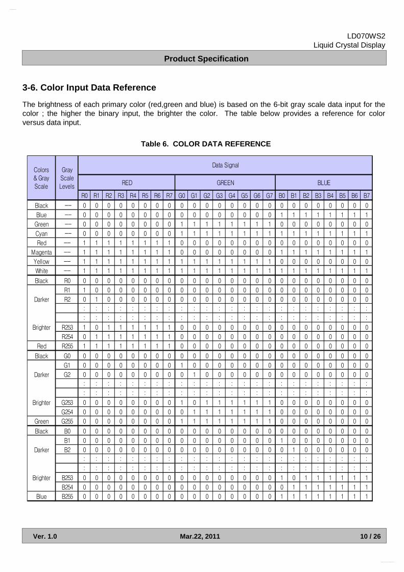
3-6. Color Input Data Reference
The brightness of each primary color (red,green and blue) is based on the 6-bit gray scale data input for thecolor ; the higher the binary input, the brighter the color. The table below provides a reference for color versus data input.
Table 6. COLOR DATA REFERENCE
R0 R1 R2 R3 R4 R5 R6 R7 G0 G1 G2 G3 G4 G5 G6 G7 B0 B1 B2 B3 B4 B5 B6 B7
Black -- 0 0 0 0 0 0 0 0 0 0 0 0 0 0 0 0 0 0 0 0 0 0 0 0
Blue -- 0 0 0 0 0 0 0 0 0 0 0 0 0 0 0 0 1 1 1 1 1 1 1 1
Green -- 0 0 0 0 0 0 0 0 1 1 1 1 1 1 1 1 0 0 0 0 0 0 0 0
Cyan -- 0 0 0 0 0 0 0 0 1 1 1 1 1 1 1 1 1 1 1 1 1 1 1 1
Red -- 1 1 1 1 1 1 1 1 0 0 0 0 0 0 0 0 0 0 0 0 0 0 0 0
Magenta -- 1 1 1 1 1 1 1 1 0 0 0 0 0 0 0 0 1 1 1 1 1 1 1 1
Yellow -- 1 1 1 1 1 1 1 1 1 1 1 1 1 1 1 1 0 0 0 0 0 0 0 0
White -- 1 1 1 1 1 1 1 1 1 1 1 1 1 1 1 1 1 1 1 1 1 1 1 1
Black R0 0 0 0 0 0 0 0 0 0 0 0 0 0 0 0 0 0 0 0 0 0 0 0 0
R1 1 0 0 0 0 0 0 0 0 0 0 0 0 0 0 0 0 0 0 0 0 0 0 0
Darker R2 0 1 0 0 0 0 0 0 0 0 0 0 0 0 0 0 0 0 0 0 0 0 0 0
: : : : : : : : : : : : : : : : : : : : : : : :
: : : : : : : : : : : : : : : : : : : : : : : :
Brighter R253 1 0 1 1 1 1 1 1 0 0 0 0 0 0 0 0 0 0 0 0 0 0 0 0
R254 0 1 1 1 1 1 1 1 0 0 0 0 0 0 0 0 0 0 0 0 0 0 0 0
Red R255 1 1 1 1 1 1 1 1 0 0 0 0 0 0 0 0 0 0 0 0 0 0 0 0
Black G0 0 0 0 0 0 0 0 0 0 0 0 0 0 0 0 0 0 0 0 0 0 0 0 0
G1 0 0 0 0 0 0 0 0 1 0 0 0 0 0 0 0 0 0 0 0 0 0 0 0
Darker G2 0 0 0 0 0 0 0 0 0 1 0 0 0 0 0 0 0 0 0 0 0 0 0 0
: : : : : : : : : : : : : : : : : : : : : : : :
: : : : : : : : : : : : : : : : : : : : : : : :
Brighter G253 0 0 0 0 0 0 0 0 1 0 1 1 1 1 1 1 0 0 0 0 0 0 0 0
G254 0 0 0 0 0 0 0 0 0 1 1 1 1 1 1 1 0 0 0 0 0 0 0 0
Green G255 0 0 0 0 0 0 0 0 1 1 1 1 1 1 1 1 0 0 0 0 0 0 0 0
Black B0 0 0 0 0 0 0 0 0 0 0 0 0 0 0 0 0 0 0 0 0 0 0 0 0
B1 0 0 0 0 0 0 0 0 0 0 0 0 0 0 0 0 1 0 0 0 0 0 0 0
Darker B2 0 0 0 0 0 0 0 0 0 0 0 0 0 0 0 0 0 1 0 0 0 0 0 0
: : : : : : : : : : : : : : : : : : : : : : : :
: : : : : : : : : : : : : : : : : : : : : : : :
Brighter B253 0 0 0 0 0 0 0 0 0 0 0 0 0 0 0 0 1 0 1 1 1 1 1 1
B254 0 0 0 0 0 0 0 0 0 0 0 0 0 0 0 0 0 1 1 1 1 1 1 1
Blue B255 0 0 0 0 0 0 0 0 0 0 0 0 0 0 0 0 1 1 1 1 1 1 1 1
Data SignalColors& GrayScale
GrayScaleLevels
RED GREEN BLUE
www.DataSheet.co.kr
Datasheet pdf - http://www.DataSheet4U.net/

Product Specification
11 / 26
LD070WS2Liquid Crystal Display
Ver. 1.0 Mar.22, 2011
3-7. Power Sequence
[Note 1] Valid Data is Data to meet “3-3. LVDS Signal Timing Specifications”[Note 2] Please avoid floating state of interface signal at invalid period.[Note 3] When the interface signal is invalid, be sure to pull down the power supply for LCD VCC to 0V.[Note 4] LED power must be turn on after power supply for LCD and interface signal are valid.
Table 7. POWER SEQUENCE TABLE
T6
Interface Signal, Vi
(LVDS Signal of Transmitter)
LED Power
Power Supply For LCDVCC
90%
10%10%0V
90%
T1 T2T5
OFFOFF LED ON
T7
T3
-(ms)50-0T5
-(ms)--200T3
-
-
-
-
-
Remark
(ms)--400T7
(ms)10-3T6
(ms)--200T4
(ms)16-0T2
(ms)10-0.5T1
Max.Typ.Min.
UnitsValueParameter
T4
Valid Data
Initial 3-Wire Command
www.DataSheet.co.kr
Datasheet pdf - http://www.DataSheet4U.net/
Product Specification
12 / 26
LD070WS2Liquid Crystal Display
Ver. 1.0 Mar.22, 2011
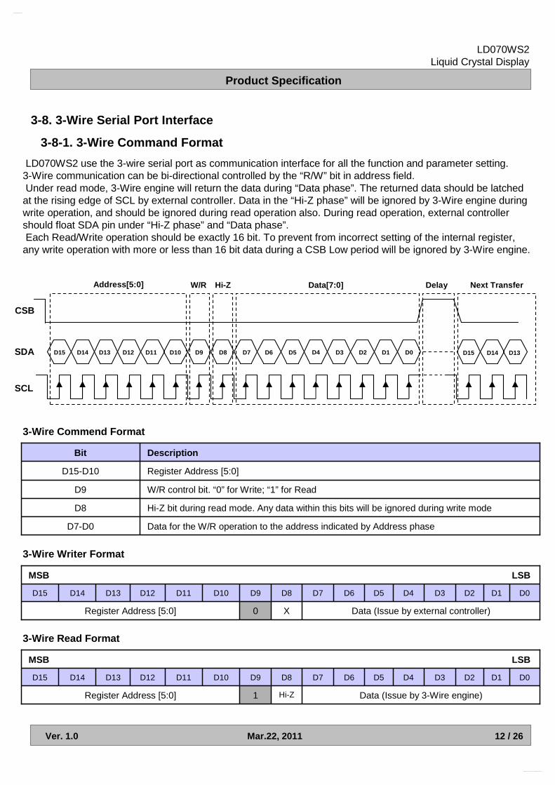
3-8. 3-Wire Serial Port Interface
3-8-1. 3-Wire Command Format
D15 D14 D13 D12 D11 D10 D9 D8 D7 D6 D5 D4 D3 D2 D1 D0 D15 D14 D13
CSB
SDA
SCL
Address[5:0] W/R Hi-Z Data[7:0] Delay Next Transfer
LD070WS2 use the 3-wire serial port as communication interface for all the function and parameter setting.3-Wire communication can be bi-directional controlled by the “R/W” bit in address field. Under read mode, 3-Wire engine will return the data during “Data phase”. The returned data should be latched
at the rising edge of SCL by external controller. Data in the “Hi-Z phase” will be ignored by 3-Wire engine during write operation, and should be ignored during read operation also. During read operation, external controller should float SDA pin under “Hi-Z phase” and “Data phase”.Each Read/Write operation should be exactly 16 bit. To prevent from incorrect setting of the internal register,
any write operation with more or less than 16 bit data during a CSB Low period will be ignored by 3-Wire engine.
Data for the W/R operation to the address indicated by Address phase
Hi-Z bit during read mode. Any data within this bits will be ignored during write mode
W/R control bit. “0” for Write; “1” for Read
Register Address [5:0]
Description
D9
D8
D7-D0
D15-D10
Bit
3-Wire Commend Format
Data (Issue by external controller)X0
D0D1D2D3D4D5D6D7D8D9D10D11D12D13D14
Register Address [5:0]
D15
MSB LSB
3-Wire Writer Format
Data (Issue by 3-Wire engine)Hi-Z1
D0D1D2D3D4D5D6D7D8D9D10D11D12D13D14
Register Address [5:0]
D15
MSB LSB
3-Wire Read Format
www.DataSheet.co.kr
Datasheet pdf - http://www.DataSheet4U.net/

Product Specification
13 / 26
LD070WS2Liquid Crystal Display
Ver. 1.0 Mar.22, 2011
3-8-2. 3-Wire Control Register
PWR_EN
-
SHLR
UPDN
STBYB
GRB
DCLKPOL
MODE
Designation
POWER enable.PWR_EN = H , enable PWM , Charge pump and VCOM bufferPWR_EN = L , disable PWM , Charge pump and VCOM buffer (Default)
Reserved
Right/Left sequence control of source driver.SHLR=”0”, Shift left: Last data=S1<-S2<-S3 … <-S960=First data.SHLR=”1”, Shift right: First data=S1->S2->S3 … ->S960=Last data. (Default)
G Gate Up or Down scan control.UPDN = “0”, STV2 output vertical start pulse and UD pin output logical “0” to Gate driver.(Default)UPDN = “1”, STV1 output vertical start pulse and UD pin output logical “1” to Gate driver.
Standby mode selection bit.STBYB=”0”, Timing control, driver and DC-DC converter, are off, and all outputs areHigh-Z.STBYB=”1”, Normal operation. (Default)
Global reset bit.GRB=”0”, The controller is in reset state.GRB=”1”, Normal operation. (Default)
DCLK polarity control bit.DCLKPOL=”0”: Data sampling at DCLK falling edge. (Default)DCLKPOL=”1”: Data sampling at DCLK rising edge.
DE / SYNC mode select.MODE=”0”, HSD/VSD mode.MODE=”1”, DE mode. (Default)
Description
R0[5]
R0[6]
R0[3]
R0[2]
R0[7]
R0[4]
R0[1]
R0[0]
Address
R00: System Control Register
R01: System Control Register
CABC_EN[1:0]
HFRC
DITHER
BIST
RES[1:0]
Designation
CABC H/W enable pin. Normally pull low.When CABC_EN=”00”, CABC OFF. (Default mode)When CABC_EN=”01”, User interface Image.When CABC_EN=”10”, Still Picture.When CABC_EN=”11”, Moving Image.
H-FRC selection. Normally pull lowHFRC = H : H-FRC enableHFRC = L : H-FRC disable (Default)If DITHER = H and HFRC = L : enable only FRC/dithering functionIf DITHER = L , disable dithering function(H-FRC and FRC both disable)
Dithering function enable control.DITHER = “1”, Enable internal dithering functionDITHER = “0”, Disable internal dithering function (Default)
Normal Operation/BIST pattern select.BIST = H : BIST(DCLK input is not needed)BIST = L : Normal Operation (Default)
Display resolution selection.RES[1:0] = “01”, for 1024(RGB)*768 display resolution(dual or cascade)RES[1:0] = “00”, for 1024(RGB)*600 display resolution(dual or cascade) (Default)RES[1:0] = “10”, for 800(RGB)*600 display resolution(dual or cascade)
(601~936 channel disable )RES[1:0] = “11”, for 800(RGB)*480 display resolution(dual or cascade)
(601~936 channel disable )
Reserved
Description
R1[7:6]
R1[4]
R1[3]
R1[5]
R1[2:1]
R1[0]
Address
www.DataSheet.co.kr
Datasheet pdf - http://www.DataSheet4U.net/

Product Specification
14 / 26
LD070WS2Liquid Crystal Display
Ver. 1.0 Mar.22, 2011
3-8-2. 3-Wire Control Register
-
NBW
-
Designation
Reserved
Normally black or normally white setting.NBW = H : Normally blackNBW = L : Normally white (Default)
Reserved
Description
R2[7]
R2[6]
R2[5:0]
Address
R02: System Control Register
R03: Gate on sequence Controller Register
-
Frame
SEL[1:0]
Designation
Reserved
Frame inverse or not select.FRAME = “1”, UniformFRAME = “0”, Frame inverse (Default)
Gate on sequence select
Description
R3[7:3]
R3[2]
R3[1:0]
Address
Z(Default)00
01
Z + 11
1
SEL[1]
0
Pin control functionSEL[0]
TEST_mode(1)
Designation
Enter test mode(1)TEST_mode = 8’h5F, enterTEST_mode = other exit (Default)
Description
R0E[7:0]
Address
TEST_mode(2)
Designation
Enter test mode(2)TEST_mode = 8’hA4, enterTEST_mode = other exit (Default)
Description
R0F[7:0]
Address
R0E:Test mode (1)
R0F: Test mode (2)
OE_WIDTH
Designation
Inversion type select. Enter Test mode(1) and (2) first. Then R0D setting will be activeTEST_mode = 8’h00, increase charging time
Description
R0D[7:0]
Address
R0D:Charing time control (3)
www.DataSheet.co.kr
Datasheet pdf - http://www.DataSheet4U.net/

Product Specification
15 / 26
LD070WS2Liquid Crystal Display
Ver. 1.0 Mar.22, 2011
EQC_ADJ
Designation
Inversion type select. Enter Test mode(1) and (2) first. Then R10 setting will be activeEQC_ADJ = 8’h43, adjust charge sharing time
Description
R02[7:0]
Address
R02:Charge sharing control (4)
BIAS_TRIG
Designation
Inversion type select. Enter Test mode(1) and (2) first. Then R10 setting will be activeBIAS_TRIG = 8’h28, trigger bias reduction
Description
R0A[7:0]
Address
R0A: BIAS current control (5)
INV
Designation
Inversion type select. Enter Test mode(1) and (2) first. Then R10 setting will be active2line / 1dot = 8’h411line / 1dot = 8’h01 (Default)
Description
R10F[7:0]
Address
R10: Inversion architecture
※※※※ Recommend Register Setting (CABC Off Mode)Register write sequence : R00�R00�R01�R02�R0E�R0F�R0D�R02�R0A�R10 �R00If you don’t use register write sequence, it may cause faulty operation.
D15 D14 D13 D12 D11 D10 D9 D8 D7 D6 D5 D4 D3 D2 D1 D0
R00 0 0 0 0 0 0 0 0 0 0 1 0 0 0 0 1 Reset
R00 0 0 0 0 0 0 0 0 1 0 1 0 0 1 0 1 Into Standby mode
R01 0 0 0 0 0 1 0 0 0 0 1 1 0 0 0 0 Enable FRC/Dither (CABC Off Mode)
R02 0 0 0 0 1 0 0 0 0 1 0 0 0 0 0 0 Enable Normally Black
R0E 0 0 1 1 1 0 0 0 0 1 0 1 1 1 1 1 Enter Test mode(1)
R0F 0 0 1 1 1 1 0 0 1 0 1 0 0 1 0 0 Enter Test mode(2)
R0D 0 0 1 1 0 1 0 0 0 0 0 0 0 0 0 0 Increase line charging time
R02 0 0 0 0 1 0 0 0 0 1 0 0 0 0 1 1 Adjust charge sharing time
R0A 0 0 1 0 1 0 0 0 0 0 1 0 1 0 0 0 Trigger bias reduction
R10 0 1 0 0 0 0 0 0 0 1 0 0 0 0 0 1 Adopt 2 Line / 1 Dot
R00 0 0 0 0 0 0 0 0 1 0 1 0 1 1 0 1 PWM On, Released standby mode
www.DataSheet.co.kr
Datasheet pdf - http://www.DataSheet4U.net/
Product Specification
16 / 26
LD070WS2Liquid Crystal Display
Ver. 1.0 Mar.22, 2011
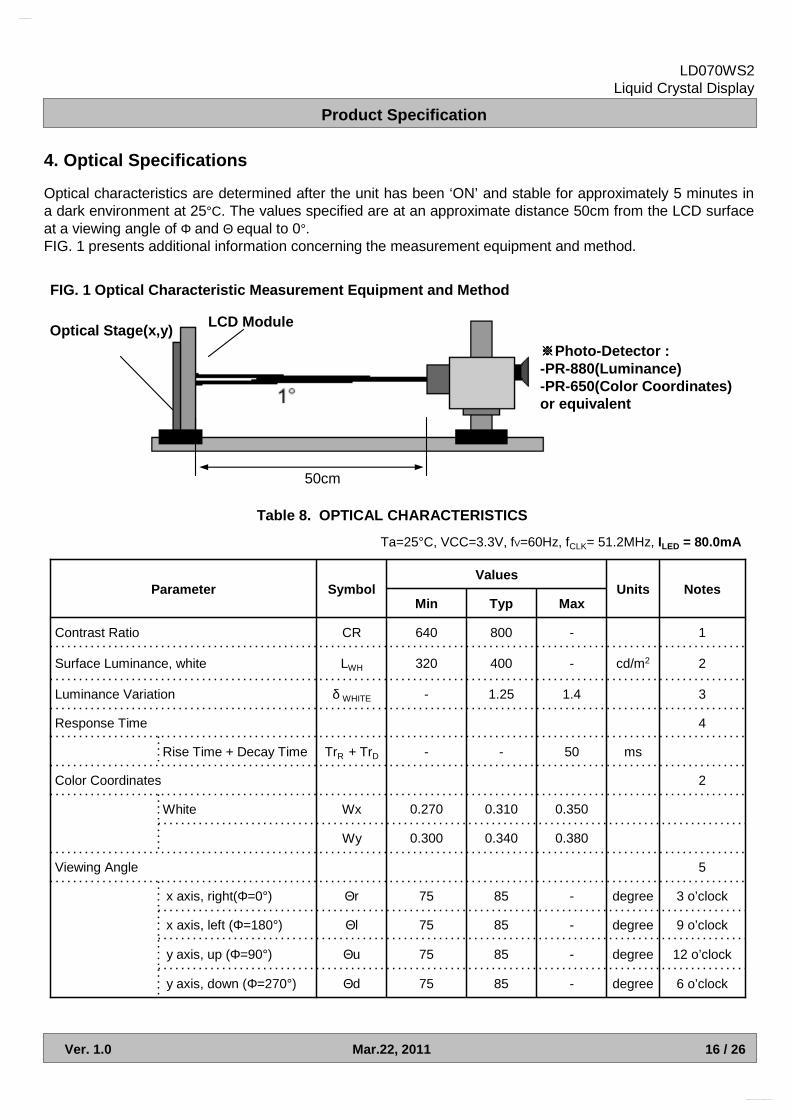
4. Optical Specifications
FIG. 1 Optical Characteristic Measurement Equipment and Method
Table 8. OPTICAL CHARACTERISTICS
Ta=25°C, VCC=3.3V, fV=60Hz, fCLK= 51.2MHz, ILED = 80.0mA
ms50--TrR + TrDRise Time + Decay Time
5Viewing Angle
2Color Coordinates
4Response Time
0.3500.3100.270WxWhite
y axis, down (Φ=270°)
y axis, up (Φ=90°)
x axis, left (Φ=180°)
x axis, right(Φ=0°) 3 o’clockdegree-8575Θr
9 o’clockdegree-8575Θl
12 o’clockdegree-8575Θu
6 o’clockdegree-8575Θd
0.3800.3400.300Wy
31.41.25-δ WHITELuminance Variation
MaxTypMin
1-800640CRContrast Ratio
2cd/m2-400320LWHSurface Luminance, white
Parameter Symbol NotesUnitsValues
LCD ModuleOptical Stage(x,y)
※※※※Photo-Detector :-PR-880(Luminance)-PR-650(Color Coordinates)or equivalent
50cm
Optical characteristics are determined after the unit has been ‘ON’ and stable for approximately 5 minutes in a dark environment at 25°C. The values specified are at an approximate distance 50cm from the LCD surface at a viewing angle of Φ and Θ equal to 0°.FIG. 1 presents additional information concerning the measurement equipment and method.
www.DataSheet.co.kr
Datasheet pdf - http://www.DataSheet4U.net/
Product Specification
17 / 26
LD070WS2Liquid Crystal Display
Ver. 1.0 Mar.22, 2011
[Note 4-1] Contrast Ratio(CR) is defined mathematically as
Surface Luminance with all white pixelsContrast Ratio =
Surface Luminance with all black pixels
[Note 4-2] Surface luminance is measured at the center point(L1) of the LCD with all pixels displaying white at the distance of 50cm by PR-880. Color Coordinates are measured at the center point(L1) of the LCD with all pixels displaying red, green, blue and white at the distance of 50cm by PR-650. For more information, refer to the FIG 1 and FIG 2.
[Note 4-3] Luminance % uniformity is measured for 9 point For more information see FIG 2.δ WHITE = Maximum(L1,L2, ….. L9) ÷ Minimum(L1,L2, ….. L9)
[Note 4-4] Response time is the time required for the display to transition from white to black (Rise Time, TrR) and from black to white(Decay Time, TrD). For additional information see FIG 3.
[Note 4-5] Viewing angle is the angle at which the contrast ratio is greater than 10. The angles are determined for the horizontal or x axis and the vertical or y axis with respect to the z axis which is normal to the LCD surface. For more information see FIG 4.
www.DataSheet.co.kr
Datasheet pdf - http://www.DataSheet4U.net/

Product Specification
18 / 26
LD070WS2Liquid Crystal Display
Ver. 1.0 Mar.22, 2011
FIG. 3 Response Time
The response time is defined as the following figure and shall be measured by switching the input signal for “black” and “white”.`
TrD
10090
100
%
Optical
Response
black white
FIG. 2 Luminance
<measuring point for surface luminance & measuring point for luminance variation>
L1
H
H/2
V/2
V
L2 L3 L4
L5 L6
L7 L8 L9
H/4
*H,V : ACTIVE AREA
V/4
TrR
black
www.DataSheet.co.kr
Datasheet pdf - http://www.DataSheet4U.net/

Product Specification
19 / 26
LD070WS2Liquid Crystal Display
Ver. 1.0 Mar.22, 2011
FIG. 4 Viewing angle
<Dimension of viewing angle range>
Normal
YEye
φ
θ
φ = 0° ,Right
φ = 180° ,Left
φ = 270° ,Down
φ = 90°, Up
Driver IC side
www.DataSheet.co.kr
Datasheet pdf - http://www.DataSheet4U.net/
Product Specification
20 / 26
LD070WS2Liquid Crystal Display
Ver. 1.0 Mar.22, 2011
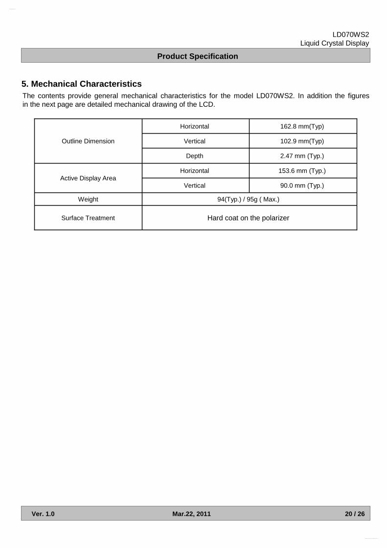
5. Mechanical CharacteristicsThe contents provide general mechanical characteristics for the model LD070WS2. In addition the figuresin the next page are detailed mechanical drawing of the LCD.
90.0 mm (Typ.)Vertical
Hard coat on the polarizerSurface Treatment
94(Typ.) / 95g ( Max.)Weight
102.9 mm(Typ)Vertical
2.47 mm (Typ.)Depth
153.6 mm (Typ.)HorizontalActive Display Area
162.8 mm(Typ)Horizontal
Outline Dimension
www.DataSheet.co.kr
Datasheet pdf - http://www.DataSheet4U.net/

Product Specification
21 / 26
LD070WS2Liquid Crystal Display
Ver. 1.0 Mar.22, 2011
<FRONT VIEW> Unit:[mm], General tolerance: ± 0.3mm
“ FOR REFERENCE ONLY ”
www.DataSheet.co.kr
Datasheet pdf - http://www.DataSheet4U.net/
Product Specification
22 / 26
LD070WS2Liquid Crystal Display
Ver. 1.0 Mar.22, 2011
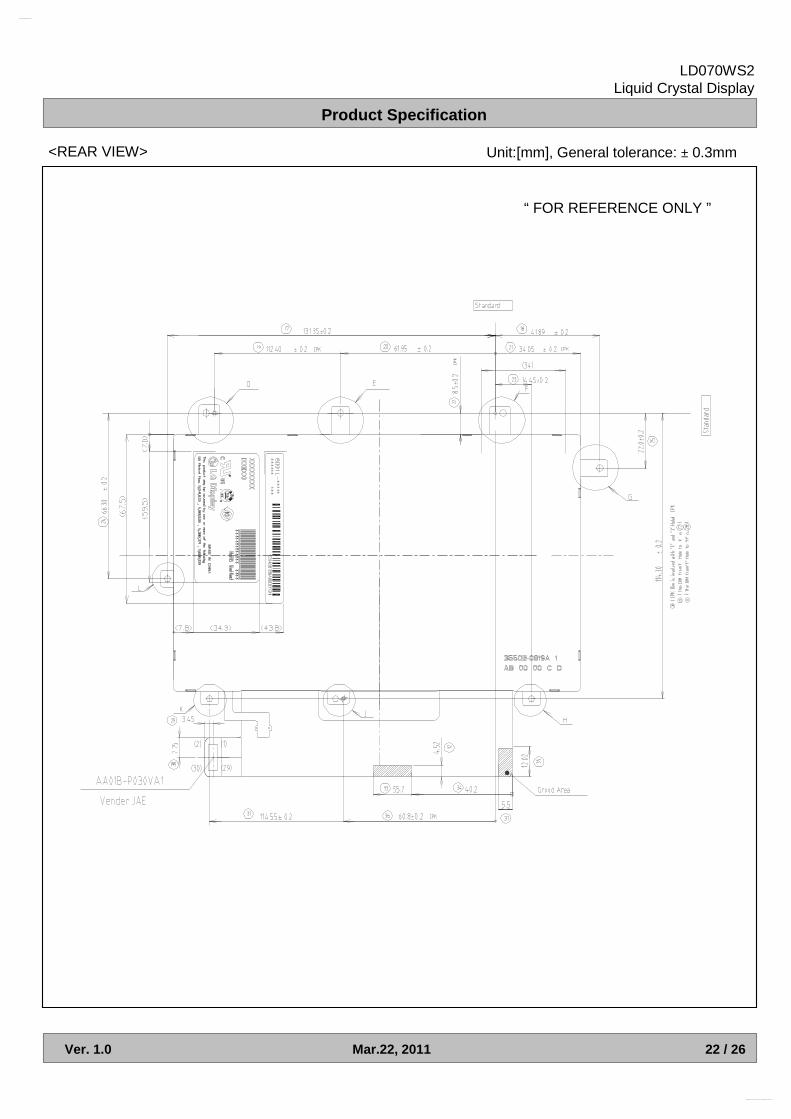
<REAR VIEW> Unit:[mm], General tolerance: ± 0.3mm
`
“ FOR REFERENCE ONLY ”
www.DataSheet.co.kr
Datasheet pdf - http://www.DataSheet4U.net/

Product Specification
23 / 26
LD070WS2Liquid Crystal Display
Ver. 1.0 Mar.22, 2011
6. International Standards
6-1. Safety
c) EN 60950-1:2006 + A11:2009, European Committee for Electrotechnical Standardization(CENELEC).Information Technology Equipment - Safety - Part 1 : General Requirements.
a) UL 60950-1, Second Edition, Underwriters Laboratories Inc.Information Technology Equipment - Safety - Part 1 : General Requirements.
b) CAN/CSA C22.2 No.60950-1-07, Second Edition, Canadian Standards Association.Information Technology Equipment - Safety - Part 1 : General Requirements.
6-2. Environment
a) RoHS, Directive 2002/95/EC of the European Parliament and of the council of 27 January 2003
www.DataSheet.co.kr
Datasheet pdf - http://www.DataSheet4U.net/
Product Specification
24 / 26
LD070WS2Liquid Crystal Display
Ver. 1.0 Mar.22, 2011
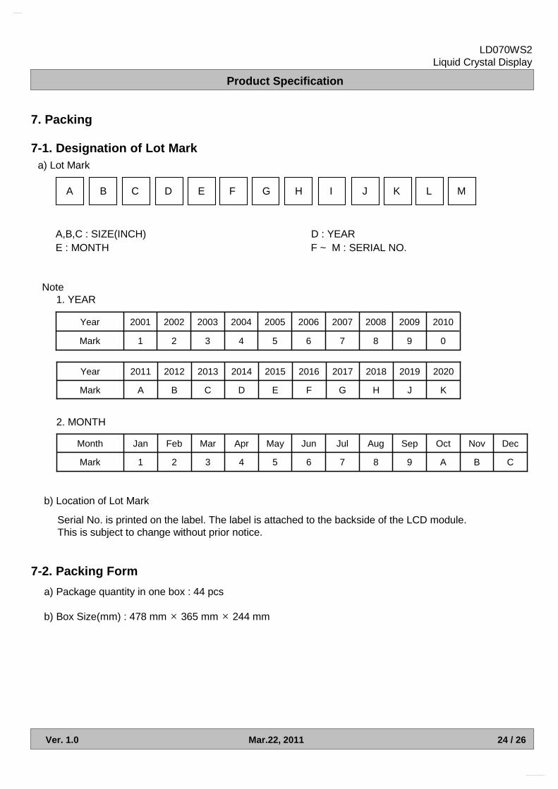
7. Packing
7-1. Designation of Lot Mark
7-2. Packing Form
a) Lot Mark
A B C D E F G H I J K L M
A,B,C : SIZE(INCH) D : YEAR E : MONTH F ~ M : SERIAL NO.
Note1. YEAR
2. MONTH
B
Nov
Mark
Month
A
Oct
6
Jun
7
Jul
8
Aug
9
Sep
4
Apr
5
May
C321
DecMarFebJan
b) Location of Lot Mark
Serial No. is printed on the label. The label is attached to the backside of the LCD module.This is subject to change without prior notice.
Mark
Year
0
2010
6
2006
7
2007
8
2008
9
2009
4
2004
5
2005
321
200320022001
a) Package quantity in one box : 44 pcs
b) Box Size(mm) : 478 mm × 365 mm × 244 mm
Mark
Year
K
2020
F
2016
G
2017
H
2018
J
2019
D
2014
E
2015
CBA
201320122011
www.DataSheet.co.kr
Datasheet pdf - http://www.DataSheet4U.net/

Product Specification
25 / 26
LD070WS2Liquid Crystal Display
Ver. 1.0 Mar.22, 2011
8. Precautions
Please pay attention to the followings when you use this TFT LCD module.
8-1. Mounting precautions
(1) You must mount a module using holes arranged in four corners or four sides.(2) You should consider the mounting structure so that uneven force (ex. Twisted stress) is not applied to the
module. And the case on which a module is mounted should have sufficient strength so that external force is not transmitted directly to the module.
(3) Please attach the surface transparent protective plate to the surface in order to protect the polarizer.Transparent protective plate should have sufficient strength in order to the resist external force.
(4) You should adopt radiation structure to satisfy the temperature specification.(5) Acetic acid type and chlorine type materials for the cover case are not desirable because the former
generates corrosive gas of attacking the polarizer at high temperature and the latter causes circuit break by electro-chemical reaction.
(6) Do not touch, push or rub the exposed polarizers with glass, tweezers or anything harder than HBpencil lead. And please do not rub with dust clothes with chemical treatment.Do not touch the surface of polarizer for bare hand or greasy cloth.(Some cosmetics are detrimentalto the polarizer.)
(7) When the surface becomes dusty, please wipe gently with absorbent cotton or other soft materials like chamois soaks with petroleum benzene. Normal-hexane is recommended for cleaning the adhesives used to attach front / rear polarizers. Do not use acetone, toluene and alcohol because they cause chemical damage to the polarizer.
(8) Wipe off saliva or water drops as soon as possible. Their long time contact with polarizer causes deformations and color fading.
(9) Do not open the case because inside circuits do not have sufficient strength.
8-2. Operating precautions
(1) The spike noise causes the mis-operation of circuits. It should be lower than following voltage : V=± 200mV(Over and under shoot voltage)
(2) Response time depends on the temperature.(In lower temperature, it becomes longer.)(3) Brightness depends on the temperature. (In lower temperature, it becomes lower.)
And in lower temperature, response time(required time that brightness is stable after turned on) becomeslonger.
(4) Be careful for condensation at sudden temperature change. Condensation makes damage to polarizer or electrical contacted parts. And after fading condensation, smear or spot will occur.
(5) When fixed patterns are displayed for a long time, remnant image is likely to occur.(6) Module has high frequency circuits. Sufficient suppression to the electromagnetic interference shall be
done by system manufacturers. Grounding and shielding methods may be important to minimized theinterference.
(7) This module is not designed to attach TSP(touch screen panels). If TSP is applied, LPL can't guaranteethe ‘Ripple’ related problems.
www.DataSheet.co.kr
Datasheet pdf - http://www.DataSheet4U.net/
Product Specification
26 / 26
LD070WS2Liquid Crystal Display
Ver. 1.0 Mar.22, 2011
Since a module is composed of electronic circuits, it is not strong to electrostatic discharge. Make certain that treatment persons are connected to ground through wrist band etc. And don’t touch interface pin directly.
9-3. Electrostatic discharge control
Strong light exposure causes degradation of polarizer and color filter.
9-4. Precautions for strong light exposure
9-5. Storage
(1) When the protection film is peeled off, static electricity is generated between the film and polarizer.This should be peeled off slowly and carefully by people who are electrically grounded and with wellion-blown equipment or in such a condition, etc.
(2) The protection film is attached to the polarizer with a small amount of glue. If some stress is appliedto rub the protection film against the polarizer during the time you peel off the film, the glue is apt toremain on the polarizer.Please carefully peel off the protection film without rubbing it against the polarizer.
(3) When the module with protection film attached is stored for a long time, sometimes there remains avery small amount of glue still on the polarizer after the protection film is peeled off.
(4) You can remove the glue easily. When the glue remains on the polarizer surface or its vestige isrecognized, please wipe them off with absorbent cotton waste or other soft material like chamoissoaked with normal-hexane.
9-6. Handling precautions for protection film
When storing modules as spares for a long time, the following precautions are necessary.
(1) Store them in a dark place. Do not expose the module to sunlight or fluorescent light. Keep the temperature between 5°C and 35°C at normal humidity.
(2) The polarizer surface should not come in contact with any other object.It is recommended that they be stored in the container in which they were shipped.
www.DataSheet.co.kr
Datasheet pdf - http://www.DataSheet4U.net/