Reconfigurable Ultrasonic Smart Sensor Platform for ...eoruklu/IIT/Publications_files/Review Copy...
40
Review Copy 1 Reconfigurable Ultrasonic Smart Sensor Platform for Nondestructive Evaluation and Imaging Applications Professor J. Saniie, Professor E. Oruklu, S. Gilliland and Professor S. Aslan Abstract: In this chapter, a Reconfigurable Ultrasonic Smart Sensor Platform (RUSSP) for real-time signal analysis and image processing is presented. The RUSSP is designed to facilitate the development and implementation of ultrasonic signal processing algorithms with embedded software and reconfigurable hardware. It provides the opportunity to explore the full design space including software only, hardware only, and hardware/software co-design architectures. Multiple case studies are investigated including real-time ultrasonic flaw detection, signal decomposition and parameter estimation on the RUSSP which hosts a Linux operating system and reconfigurable fabric. Keywords: Ultrasonic signal processing, system-on-chip, non-destructive testing, flaw detection, field-programmable gate arrays, reconfigurable computing
-
Upload
truongdiep -
Category
Documents
-
view
222 -
download
0
Transcript of Reconfigurable Ultrasonic Smart Sensor Platform for ...eoruklu/IIT/Publications_files/Review Copy...

Review Copy
1
Reconfigurable Ultrasonic Smart Sensor Platform for
Nondestructive Evaluation and Imaging Applications
Professor J. Saniie, Professor E. Oruklu, S. Gilliland and Professor S. Aslan
Abstract:
In this chapter, a Reconfigurable Ultrasonic Smart Sensor Platform (RUSSP) for real-time signal
analysis and image processing is presented. The RUSSP is designed to facilitate the development
and implementation of ultrasonic signal processing algorithms with embedded software and
reconfigurable hardware. It provides the opportunity to explore the full design space including
software only, hardware only, and hardware/software co-design architectures. Multiple case
studies are investigated including real-time ultrasonic flaw detection, signal decomposition and
parameter estimation on the RUSSP which hosts a Linux operating system and reconfigurable
fabric.
Keywords: Ultrasonic signal processing, system-on-chip, non-destructive testing, flaw
detection, field-programmable gate arrays, reconfigurable computing

Review Copy
2
Reconfigurable Ultrasonic Smart Sensor Platform for Nondestructive Evaluation
and Imaging Applications
Jafar Saniie, Erdal Oruklu, Spenser Gilliland and Semih Aslan
1.1 Introduction
In recent years, high speed signal analysis has been used to modernize methods of ultrasonic
measurement, imaging, and testing (Weber, et al. 2011; Oruklu and Saniie 2009; Lu et al. 2006;
Goldsmith, et al. 2008; Kunita et al. 2008). Ultrasonic technologies have continued to gain in
popularity due to their high precision, low cost and shrinking footprint of the sensors. It is now
possible to measure object properties and produce high resolution images and video that provide
a complete three-dimensional view of the internal physical geometrical characteristics within an
object. These capabilities have given new insight into fields such as structural health
monitoring, material science, and medical imaging.
This chapter presents the design and application of an FPGA-based Reconfigurable Ultrasonic
Smart Sensor Platform (RUSSP). The proposed system provides real-time signal processing for
nondestructive evaluation (NDE) and imaging applications using ultrasonic sensors ranging from
20 KHz to 20 MHz operational frequencies. Specifically, hardware implementations suitable for
portable systems with networking capability are discussed. In practice, NDE of materials
requires the design of sensor array to be tightly coupled to data collection at high sampling rates
and real-time computation. For high resolution imaging, ultrasonic measurements involve
sensors operating in MHz frequency range. This results in a significant computational load for
embedded systems. In order to address these challenges, we present an exploration of

Review Copy
3
architectural variations and realizations that are designed to efficiently achieve the real-time
performance goals and constraints. A smart sensor system is presented for ultrasonic pulse-echo
measurements targeting flaw detection and parametric echo classification applications. For real-
time implementation, an FPGA-based system is developed on Xilinx Virtex-5 FPGA platform.
In order to achieve high throughput and robust performance, several design methodologies are
investigated; including the execution of the flaw detection and echo classification algorithms on
an embedded microprocessor configured within the FPGA running a Linux operating system, the
creation of a dedicated hardware solution, use of hardware/software (HW/SW) co-design
methods, and network enabled operations.
Advances in digital signal processing (DSP) hardware facilitate the development of low cost and
portable ultrasound sensor devices. Instead of requiring multiple discrete components, an
ultrasound measurement system can now be built using just DSP hardware and an analog-to-
digital converter (ADC). The processing requirements for ultrasonic DSP hardware have
traditionally been met using Application Specific Integrated Circuits (ASIC) which provide very
high performance but have substantial costs and cannot be reconfigured for different
applications, thereby limiting their availability to low volume applications and research. Today,
many ultrasonic applications are now able to fit within the capabilities of reconfigurable logic
such as Field Programmable Gate Arrays (FPGA) (Rodriguez-Andina et al. 2007). An FPGA
provides all the parallelism capabilities of an ASIC while allowing the device to be
reprogrammed for a given application. This allows a single FPGA to be used in testing multiple
algorithms that would traditionally require multiple manufacturing runs (or additional die area)
to implement in an ASIC. DSP and FPGAs have opened additional avenues for ultrasound

Review Copy
4
signal analysis techniques in both industry and academia. FPGAs satisfy the demands of
researchers due to their relatively low cost, reconfigurability, and ASIC-like parallelism and
performance capabilities. Within the industry, time to market and budget limitations have forced
even shorter development periods. FPGA based systems are well suited for smart sensor
ultrasonic imaging applications due to having a much shorter development time and lower costs
than that of an ASIC.
The proposed Reconfigurable Ultrasonic Smart Sensor Platform (RUSSP) provides real-time
signal analysis and image processing for a full range of ultrasonic testing and imaging
applications. The project aims to streamline the development and implementation of signal
processing algorithms in embedded software and reconfigurable hardware. This provides the
user with an opportunity to explore the full design space including software only, hardware only,
and hardware/software co-design. Specifically, the RUSSP provides high speed access to a 12-
bit 250 MSPS Maxim MAX1215N ADC (Maxim1215N 2012) controlled by a Xilinx
XC5VLX110T FPGA (Xilinx 2010). Access to the ultrasound data and custom IP cores is
available through a gigabit Ethernet connection managed by an embedded Linux based operating
system running on a Microblaze processor instantiated in the FPGA fabric. The major feature of
this SoC is the integration of a processor which is capable of executing platform independent C
code. The ability to execute C code allows the reuse of a substantial portion of available
software, thus reducing design and development time. This system also promotes additional
reuse at the hardware level as IP Cores are able to easily integrate with the processor.
Furthermore, the bus architecture has been integrated into an off-the-shelf operating system so
that device drivers can be easily reused.

Review Copy
5
1.2 Fundamentals of ultrasonic sensing and pulse-echo measurements
When an ultrasonic wavelet passes through materials, it loses energy and its sound pressure
decreases. This loss results from two causes, scattering and absorption, both of which can be
combined in the concept of attenuation. Scattering results when the material is not strictly
homogeneous and contains boundaries at which the acoustic impedance changes abruptly due the
difference in density and/or sound velocity at the interfaces. There are also materials which are
inhomogeneous by their nature. Typically the degree of inhomogeneity can be estimated in two
separate modes of signal analysis. A practical method is by an estimation of the attenuation
coefficient. The other widely used method is by inspection of the backscattered echoes. One of
the most popular ultrasonic imaging techniques involve transmitting extremely short burst of
sound energy into the sample and monitoring the return echo. This method is referred to as the
ultrasonic pulse-echo technique for NDE and imaging applications. Depending on the
experimental setup and the type of signal processing, one may use these received signals to
represent the data in one, two, or three dimensions.
In ultrasonic pulse-echo scanning, the received signal contains the reflected echo from physical
and geometrical variation and discontinuity within the sample under testing. The time of flight of
these echoes provides information which pertains to the depth of the reflector and the intensity
yields information about the gradient of the impedance and the size of the reflector. In practice,
identification of the reflecting surfaces becomes extremely difficult, if not impossible, due the

Review Copy
6
existence of multiple reflections. The setup for ultrasonic pulse-echo measurement using the
proposed RUSSP is shown in Figure 1.1 and Figure 1.2.
The RUSSP is designed to be an easy to use platform for developing high throughput, real-time
signal processing algorithms. The primary requirement is the use of an ultrasonic pulser to excite
the transmitting transducer. This transducer converts the electrical signal to an acoustical
radiation field. The generated ultrasonic wave both propagates and reflects echoes
corresponding to the characteristic of the propagation path in the sample under test. For example
in NDE of materials, there may be cracks or cavities created by stress during use, impurities
during manufacturing, etc. Because such cracks and cavities introduce a discontinuity within
materials, they can be observed using ultrasonic pulse-echo measurement techniques. The
reflected ultrasonic wave excites the receiving transducer which converts the transient vibration
energy into an electrical signal. In RUSSP, the backscattered and reflected echoes can be
sampled with a precision of 12 bits and up to 250 MSPS. Through experimentation, it was
determined that the pulsar/receiver can operate at a maximum trigger rate of 10 KHz.
1.3 Reconfigurable ultrasonic smart sensor platform (RUSSP)
1.3.1 System features and user interface
It is important to build a system that is convenient for both hardware and software developers by
meeting the interface requirements. The data acquisition system needs to be integrated with the
Matlab programming environment due to common use of the Matlab tool among algorithm
developers. Furthermore, Matlab can be used in the validation of the systems hardware and

Review Copy
7
software components. The Application Programming Interface (API) to communicate with the
system is based on TCP/IP using the UNIX socket API. The UNIX socket API is a commonly
used and well understood methodology for transmitting and receiving data across the Internet.
The Xilinx Embedded Development Kit software (Xilinx 2012) is used in developing RUSSP
hardware. This allows the use of self-contained pcores for hardware components of the system
and Xilinx Board Definition (XBD) files to designate the SoC design, off chip connections, and
constraints. The self-contained nature of these methods allows reuse across different
implementations of the RUSSP. Finally, the RUSSP uses a Linux based operating system which
is accessible over SSH and serial port (Corbet 2005; POSIX 2008). This provides a common
UNIX shell interface to the developer for system exploration and debugging.
1.3.2 System response and real time operational requirements
Real-time processing in the DSP context is considered as a system which is capable of
processing the incoming signal before the next signal arrives. However in relation to software
and hardware, real time constraints are: determinism, jitter, and delay. Determinism is the
requirement of a system to finish processing a required task within a finite time frame. Jitter is
the difference between the minimum and maximum response time to an external event. Delay is
the maximum time between an external event occurring and a process executing. Both DSP and
software/hardware real-time constraints are applicable to the RUSSP system.
The system must provide an interface which offers less than 5 ns jitter for use in coherent
averaging since the maximum sampling rate is 200 MSPS. This interface should provide access

Review Copy
8
to the incoming sample, a high speed memory interface, and the time in samples since the pulse
was triggered. As the bulk of the system is implemented in FPGA logic, the system is able to
guarantee strict hard real-time demands in hardware; however, software interrupt and scheduling
latencies should be contained to avoid buffer overruns when copying data from the ADC to the
memory or network. The maximum delay for a software application running on the RUSSP is
100 μs or 10 KHz. This ensures that the software is able to process a response before the next
response is acquired.
1.3.3 RUSSP architecture
The RUSSP was built using several components including a Xilinx XUPV5 FPGA development
platform (Xilinx 2010), a Maxim MAX1215N ADC Evaluation Kit (Maxim1215N 2012), a
Maxim MAX5874 DAC Evaluation Kit (Maxim5874 2012), and two Maxim MAX1536 Power
Supply Evaluation Kits (Maxim1536 2012). By integrating these components the RUSSP
system is created. The system can be miniaturized by creating a custom printed circuit board
which includes chips from each of the components above. The interconnections of these
components are presented in Figure 1.3 and the throughput of the various interfaces is presented
in Figure 1.4.
In the RUSSP design, the XUPV5's XC5VLX110T FPGA is used for signal processing. The
DDR2 memory controller is used for volatile data storage during processing. The compact flash
is used for non-volatile storage of the FPGA and software configuration. The serial port is used
for debugging and configuration. The gigabit Ethernet controller provides remote data and

Review Copy
9
control communication. The benefit of using a Virtex 5 FPGA such as the XC5VLX110T over
other FPGAs is the inclusion of DSP48 blocks. DSP48 blocks provide constant multiply and
accumulate (MAC), two operand multiply, and division capabilities. The ability to execute
MAC operations greatly increases the maximum operating frequency of digital filter
implementations. The system is capable of storing up to 256 MB of data in the DDR2 memory
for future analysis. The DDR2-400 used in RUSSP has a maximum theoretical bandwidth of
3200 MB/s and interfaces to the RUSSP though the MPMC (Multi-Port Memory Controller)
provided by Xilinx (Xilinx 2011). The gigabit Ethernet controller is connected to the processor
using the PLB (Processor Local Bus) interface and an SDMA (Soft Direct Memory Access) PIM
(Personality Interface Modules) of the MPMC (Multi-Port Memory Controller). The SDMA
PIM provides high speed scatter-gather DMA (Direct Memory Access) transfers to the Ethernet
MAC so that the processor is free to process even when data is being copied into or out of main
memory. The gigabit Ethernet is connected to the local network and provides ample bandwidth
for simultaneous command/control and data capture. The main bottleneck in RUSSP is the
throughput of the PLB bus inside the FPGA SoC. Therefore in future iterations of this design,
integration of direct memory access peripherals will be used to reduce data transfers across the
PLB bus.
The RUSSP system communicates with the user using TCP/IP on top of gigabit Ethernet. The
RUSSP system is theoretically capable of providing wired gigabit Ethernet communication at
125 MB/s. Given a packet of 1500 bytes, the total overhead for IP and Ethernet is approximately
4%. Given another 1% of overhead for TCP, leaves a total of 118.75 MB/s for data
transmission.

Review Copy
10
A block diagram of the FPGA embedded system is shown in Figure 1.4. The FPGA System-on-
chip (SoC) is based around the Processor Local Bus (PLB). PLB is a standard from IBM which
defines how components interconnect with one another in a standard bus topology. The SoC
includes the following cores from Xilinx: A multi-port memory controller (MPMC), universal
asynchronous receiver transmitter (UART), Gigabit Ethernet, System Advanced Configuration
Environment (Sys ACE) compact flash controller, timer, clock generators, and a Microblaze
processor.
The multi-port memory controller provides high speed memory access to the system. It provides
this through PIM. PIMs allow the memory to transfer data using some common patterns. There
are PIM modules for PLB, AMBA (Advanced Microcontroller Bus Architecture), DMA, Frame
Buffer, Cachelink, Locallink and a raw native interface. Three PIMs are used in our design. A
Cachelink PIM is used to interface the MPMC with the processor caches. A PLB PIM is used to
provide access to memory for the PLB bus peripherals. A DMA PIM is connected to the gigabit
Ethernet MAC to provide high speed data transfers.
The software runs on a Xilinx Microblaze processor. The Microblaze processor is a 32 bit
reduced instruction set CPU (RISC) which is unique because it allows the engineer to make
modifications to its functionality during synthesis. Notably, the processor can be configured to
include an MMU which is a requirement of the Linux kernel. The Microblaze core can be
customized to include an FPU (Floating-Point Unit) and streaming interface to either fast
simplex link or AXI (Advanced eXtensible Interface) stream interfaces. This allows the core to

Review Copy
11
have additional pseudo instructions added to the instruction set. 12 KB data and 4KB instruction
caches were chosen in order to strike a balance between resource usage and performance. The
cache is backed by the multi-port memory controller (MPMC) which interfaces to the DDR2
memory.
A timer/counter, interrupt controller and UART are present in the base system to accommodate
the requirements of Linux. The timer counter provides timer interrupts to the software system,
the interrupt controller allows multiple interrupts to be received and decoded by the software
system, and the UART provides a basic interface to the system for debugging.
1.3.4 ADC to FPGA interface
In choosing an ADC, the main goal was to design for a broad frequency spectrum of ultrasound
from 20 KHz to 20 MHz. The MAX1215N is capable of supporting up to 250 MSPS which is
above the minimum required sampling rate. This allows enough bandwidth to capture all the
received ultrasonic echoes. Assuming a 250 MHz clock, the total throughput of the ADC is 375
MB/s.
The ADC uses LVDS (low voltage differential signaling) when interfacing to the FPGA. LVDS
is a differential signaling methodology which uses a small current to generate a voltage at the
receiver. The LVDS generates a 3.5mA current on either the negative or positive (N or P) net
depending on the polarity of the signal. This is then transformed into a voltage using a
terminating resistor. The key to making a reliable and high speed connection between the FPGA
and the ADC is to use the DIFF_TERM attribute of the FPGAs IOB (Input/Output Block) for

Review Copy
12
each LVDS pair in the constraints file. This attribute turns the built-in, 100Ω, differential
termination resistor on (Xilinx 2010).
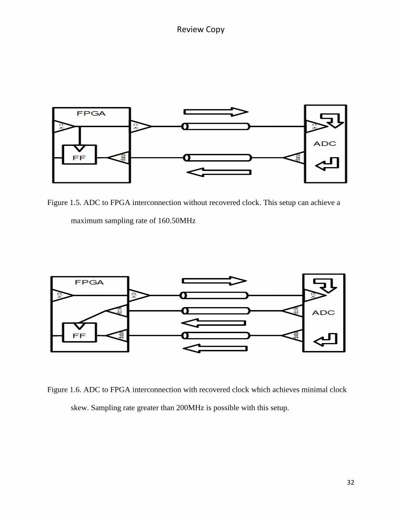
Initially, the connections between the ADC and the FPGA can be represented by Figure 1.5. The
maximum operating frequency is governed by the delay, which depends on the length of
wire and delay of the ADC. Because the edge rate of the ADC is significant with respect to the
length of wire, the line must be treated as a transmission line. The transmission line has a delay
of 170 ps/inch according to the measurement obtained in this study which compares an 18 inch
vs. 12 inch coaxial wire. For this arrangement, the total skew is approximately 6.23 ns and limits
the connection to a maximum sampling rate of 160.50 MHz.
In order to meet the 200 MHz requirement of RUSSP system, the recovered clock feature of the
ADC was implemented as shown in Figure 1.6. The recovered clock is aligned with the data
which ensures that minimal clock skew is present (assuming equal length data/clock traces).
This allows the ADC to operate at its maximum operational frequency.
1.4 Algorithms used in evaluation of RUSSP
Throughout this study, several algorithms and techniques have been implemented in the RUSSP.
Coherent averaging is used as a method for reducing electrical noise. Split Spectrum Processing
(Bilgutay et al. 1979; Newhouse et al. 1982; Saniie et al. 1988) is used as a method for reducing
Rayleigh scattering noise. Chirplet Signal Decomposition (Lu et al. 2006) is used as a method
for classifying and compressing ultrasound data. Combining these methods creates an effective
ultrasound signal classification and detection system.

Review Copy
13
1.4.1 Coherent averaging
Coherent averaging is a method for reducing the signal to noise ratio (SNR) of a pulsed signal. It
is based on acquiring multiple responses and averaging them together based on their time
difference from the start of the pulse. Given an ideal signal, corrupt by the additive noise,
, the received signal can be represented as:
(1.1)
The signal is assumed to be deterministic and the same for multiple measurements. The additive
noise is a random process with zero mean and noise embedded within multiple measurements are
assumed to be independent and identically distributed. Then, the SNR of the received signal is
defined as,
(1.2)
where indicates the expected noise power (i.e., noise variance) and
represents the signal power. Since the target is stationary and the excitation pulse is constantly
repeated, the coherent average of multiple responses can be used. Therefore, the SNR of a
coherently averaged signal can be expressed by
(1.3)
Inspection of reveals that a √ ⁄ reduction in noise amplitude is provided by coherent
averaging.

Review Copy
14
1.4.2 Split spectrum processing
Split Spectrum processing (SSP) is an algorithm used for discerning frequency diverse echoes.
The algorithm splits a broadband signals into multiple narrowband signals (N. Bilgutay et al.
1979; Newhouse et al. 1982). These signals are then post processed using algorithms such as
absolute minimization, median filtering, or more complex algorithms based on fuzzy set logic,
ordered statistics, and neural networks. The general goal is to remove the Rayleigh scattering in
a system thereby increasing the target to clutter ratio (TCR). In a given signal, there are three
types of scattering: i) Rayleigh Scattering, ii) Stochastic Scattering, and iii) Geometric
Scattering. The relationship between the size of the discontinuity and the wavelength of the
pulse determines the type of scattering created. Rayleigh scattering occurs when the object
causing the scattering is small compared to the wavelength of the ultrasound pulse. Stochastic
scattering occurs when the wavelength of the ultrasound pulse is similar in size to the measured
object. Diffusion scattering occurs when the wavelength of the ultrasound pulse is much smaller
than the size of the object. Of the three types of scattering, Rayleigh scattering and Stochastic
scattering can be considered noise for an ultrasonic flaw detection system.
The combined effects of Rayleigh scattering and stochastic scattering are known as clutter.
Clutter is a combination of the many echoes that are produced in the microstructures of a
material (i.e., grains). When an ultrasound wave scatters from grains, it produces a stationary
scatter which represents these grain scatterers. When the aggregate of all of the scatterer echoes
are combined, they produce a static noise that hides the target echo. Therefore, these scatterings
must be filtered from the signal in order to increase the SNR for the classification or detection

Review Copy
15
system and enable accurate detection of the target. When a measurement is taken using a
number of different narrowband pulses with different frequencies, the clutter echoes become
randomly distributed across the pulse frequencies and can be filtered using statistical processing.
For the performance evaluation of RUSSP, there is an emphasis on a post processing
methodology called pass-through absolute minimization. Pass-through absolute minimization
takes advantage of the special properties of absolute minimization (Newhouse et al. 1982) in
improving the signal-to-noise ratio but maintains the sign of the original signal such that the
response can be classified by other signal processing method such as chirplet signal
decomposition.
The SSP procedure has five steps as shown in Figure 1.7. The first part is data acquisition. The
second step, Fast Fourier Transform (FFT) gives the frequency spectrum of the received echo
signal. Third step, several filters split the spectrum into different frequency bands. Next step,
inverse FFT gives the time domain signal of each individual frequency band. The signals from
each individual frequency band are first normalized and then passed into a post processing block
for detection. This detection processor can employ different techniques such as averaging,
minimization, order statistic filters (e.g. minimization), or Bayesian classifiers (Saniie et al.
1988; Saniie et al. 1991; Saniie and Nagle 1992; Saniie 1992). SSP has been successfully applied
to ultrasonic flaw/target detection applications due to its robust performance.
1.4.3 Chirplet signal decomposition

Review Copy
16
Ultrasonic signals are often composed of many interfering echoes. Each echo is similar to a
chirplet and chirplets can be described with six parameters using chirplet signal decomposition
(CSD) (Lu et al. 2006; Lu et al. 2008). Therefore, CSD representation results in a major data
reduction (compression) when compared to the raw ADC data and it can be used for data storage
and assessment. Furthermore, the estimated chirplets can be used for material characterization
and system identification.
The chirplet signal can be defined as,
(1.4) This equation has six parameters where term is the time-of-arrival,
cf
is the center frequency, is the amplitude, 2 is the chirp rate, is the phase, and
1 is the
bandwidth factor of the echo. This model accurately models the echoes from ultrasound
experiments. The algorithm for CSD is as follows [Lu et al. 2008]:
1. Find the maximum location of in the time domain and use it as the initial
guess of time-of-arrival and the starting point of iteration.
2. Estimate the center frequency which maximizes the chirplet transform, given
initial guess of time-of-arrival.
3. Estimate the time-of-arrival which maximizes the chirplet transform, given the
estimated center frequency from the previous step.
4. Estimate the center frequency which maximizes the chirplet transform, given the
new estimated time-of-arrival from step 3.
5. Check convergence: If and where and are
predefined convergence conditions, then go to the next step otherwise, go back to
step 3.

Review Copy
17
6. Estimate the amplitude β and the remaining parameters , φ, and
successively.
7. Obtain the residual signal by subtracting the estimated echo from the signal.
8. Calculate energy of the residual signal ( ) and check convergence ( is
predefined convergence condition): If , STOP; otherwise go to step 1.
The method for extracting chirplet parameters utilizes the chirplet transform,
∫
(1.5) Where
is chirplet kernel and can be represent as
(
)
( (
)
)
(1.6)
],,,,2
,[ˆ12
ab c denotes the parameter vector of the chirplet used for transformation.
The first step of this method is to extract an estimated based on the maximum value in the time
domain. Then, the parameter , which has the highest correlation at , can be used as an
initial estimate. From these two values, the parameter can be estimated, followed by , θ and
and finally β. This equation for the estimation algorithm is summarized below:
| |
| |
}
(1.7)
| |
|
(1.8)

Review Copy
18
| |
|
(1.9)
| |
|
(1.10)
Chirplet signal decomposition block diagram for estimation of chirplet parameters is shown in
Figure 1.8.
1.5 Hardware realization of ultrasonic imaging algorithms using RUSSP
RUSSP is a flexible system designed to host real-time ultrasonic signal processing algorithms.
Due to the reconfigurable logic, an embedded CPU and the Linux OS, RUSSP facilitates
multiple implementation schemes such as Hardware/Software codesign for fast design time and
rapid prototyping. This section presents implementation details for four case studies including
the algorithms discussed in Section 1.4.
1.5.1 Averaging implementation
Coherent averaging heavily relies on precise synchronization between the pulse and capture logic
in order to provide accurate results. Thus, this implementation takes advantage of the
preprocessing block in the ADC as shown in Figure 1.9 to create a highly accurate
synchronization between the data acquisition capture clock and the excitation trigger pulse
applied to the ultrasonic transducer. Since the preprocessing block is clocked by the dclk of the
ADC, the timing is guaranteed to be accurate to within the frequency of the clock used to drive
the ADC.

Review Copy
19
Initially, a basic averaging implementation was developed. However, it was not possible to meet
timing with this original design. In order to explore the design space for timing closure, the
original implementation was extended to support parallel operations. In the current
configuration, the coherent averaging block is parallelized by a factor of four and can be
represented by Figure 1.10. Due to the concurrent nature of this design, the implementation is
able to reliably meet timing requirement in this system.
Coherent Since the slower distributed RAM was unable to meet the 200 MHz timing
requirement, the coherent averaging block implements its memory using Block RAMs (BRAM.)
In Xilinx FPGAs, BRAMs are faster but have a one cycle delay for access. Therefore, it takes
two clock cycles for an accumulation to occur. The first cycle is a read cycle and the second is a
write cycle. During the read cycle, the BRAM exports the value to a register. During the write
cycle, the incoming data is added to the value in the register and stored back in the BRAM.
1.5.2 Split spectrum processing (SSP) implementation
The goal of SSP is to reduce interference resulting from scatterers. An implementation of the
SSP algorithm has been instantiated inside the FPGA fabric. The SSP hardware uses FFT
followed by a basic one-zero windowing algorithm to split spectrum, inverse FFT (iFFT) to
obtain frequency-diverse signals, and pass-through absolute minimum processing to improve the
visibility of target echo in presence of clutter.

Review Copy
20
As the SSP algorithm uses a significant number of FFTs, it is important that the FFT
implementation must be highly area efficient. The most efficient IP Core available for
implementing an FFT/iFFT is the Xilinx Radix 2-Lite FFT IP Core (FFT 2012). At a transform
size of 4096 points, this IP Core has a latency of 57,539 cycles; however, it uses only two DSP
48 components, seven BRAMs, and approximately 250 slices. This low resource usage allows
up to 13 FFTs to be implemented in tandem with the other components of the RUSSP.
The SSP implementation has synthesis parameters which can be altered in EDK for changing the
number of channels, and the maximum number of samples. In the current configuration, the SSP
algorithm uses twelve channels and 4096 samples which is the maximum number possible given
the DSP48 resources available on the FPGA. For the SSP processing, the number of FFTs
required is equal to the number of channels plus one. In the current configuration, the
implementation has thirteen FFTs instantiated in the FPGA.
Control registers specify the number of samples to use, the start, width and offset of the SSP
algorithm. The implementation makes use of a memory which is used to load the samples into
the SSP algorithm and store them after processing. The memory has two ports; one is connected
to the SSP algorithm block as shown in Figure 1.11; the other is connected to the PLB bus and is
addressable by the processor.
In Figure 1.12, the results from a four channel instantiation of the SSP algorithm are shown. The
flaw echo, located at around sample number 1750, is present in each of the channels and has
unchanged amplitude. This is because the flaw echo is not a composite signal in contrast to the

Review Copy
21
clutter signal which is highly dependent on the frequency span of narrow-bands. By using a pass-
through absolute minimization processing block, the flaw signal maintains many of its original
properties, but the frequency dependent scattering signal is substantially reduced.
1.5.3 Chirplet signal decomposition (CSD) implementation
An implementation of the CSD algorithm was created in the C programming language. The
algorithm was implemented in software due to the high complexity. The basis for the
implementation is the algorithm discussed in Section 1.4.3; however, the algorithm has been
optimized by using precomputation and estimation methods. Additionally, the algorithm has
been altered to provide deterministic behavior.
The primary goal of the current implementation of the CSD algorithm is to reduce the execution
time as much as possible while maintaining an adequate SNR for echo estimation. The main
performance impediment for CSD is the correlation operations which require regenerating a
chirplet with different parameters thousands of times during each parameter estimation step in
the algorithm. By pre-computing a table of these values and manipulating this table to perform
the operation, the computation time was drastically reduced. This was accomplished by finding
expressions which could have shared parts and extracting them from the inner loops.
Furthermore, this CSD implementation takes advantage of estimation techniques to reduce the
overall computation time. By using lookup tables for cosine, sine and tangent, the total
execution time was substantially reduced with only a slight reduction in accuracy.

Review Copy
22
The CSD algorithm is enhanced by altering the non-deterministic operations such as step 5 and
step 8 from the listing in Section 1.4.3. In step 5 and step 8, the reiteration of the algorithm if the
error condition is not met makes it impossible to reliably determine the total execution time. To
gain determinism, the reiteration condition is changed such that a finite number of iterations are
performed. In our case, the number of time of arrival and frequency re-estimates (step 5) is two
and a total of fifteen echoes are extracted (step 8). These parameters ensure a total SNR of the
regenerated signal equal to approximately 10 dB. In Figure 1.13, the echoes from the CSD
algorithm are regenerated and compared to the echoes in the original signal.
1.5.4 Resource usage and timing constraints
The RUSSP implementation uses a significant portion of the FPGA resources when the SSP
algorithm is included. The total resource usage of the RUSSP with a 4, 8 and 12 channel SSP
implementation is shown in Table 1.1. In the case of a 12 channel SSP implementation, a total
of 13 hardware FFTs are implemented in the FPGA fabric and a total of 59 DSP48s are in use.
The total number of channels for the SSP implementation is limited by the total number of
DSP48s available in the system. Removal of the SSP component cuts the resource usage in half.
The RUSSP meets timing for all critical nets in the system. The system has a total of three main
clock domains: the processor clock, the ADC clock, and the SSP clock. The processor clock
meets timing at 100 MHz, the ADC clock meets timing at 200 MHz, and the SSP clock meets
timing at 100 MHz. The total execution time of the SSP implementation with a total of 2048
samples as measured from the processor is 16 ms. The testing methodology for the SSP
execution times is based on the clock_gettime(CLOCK_MONOTONIC) function. This function

Review Copy
23
returns wall clock time in a monotonic fashion such that alterations due to network time protocol
or other clock tuning would have no effect on the results.
Execution times for the CSD algorithm are listed in Table 1.2. These results show a nearly linear
increase in execution time with respect to number of echoes.
1.6 Future trends and sources of further information
For embedded ultrasonic signal processing systems, new reconfigurable hardware platforms such
as Xilinx Zynq-7000 EPP (Zynq-7000 2012) present an important evolutionary step. Zynq
combines an industry-standard ARM® dual-core Cortex™-A9 MPCore™ processing system
with Xilinx 28nm programmable logic. This platform would be ideal for RUSSP applications
since the embedded ARM processor provides a significant boost to the software execution
capabilities. Additionally, due to the penetration of embedded ARM devices, it is more
convenient to acquire code development tools, technical support and market acceptance.
Dynamic Partial Reconfiguration (DPR) also provides an interesting approach to developing
applications for the RUSSP. DPR allows users to download hardware accelerators into the
system during runtime (Desmouliers et al. 2011; Sudarsanam et al. 2010; Rossi et al. 2009; Rossi
et al. 2010; Ahmed et al. 2011). This allows applications to swap in and out their accelerators as
FPGA resources and requirements allow. In a sense, DPR achieves time-multiplexing of the
available reconfigurable fabric for multi-tasking operations. Several ultrasonic platforms already
support DPR (Oruklu & Saniie 2009; Yoon et al. 2006; Desmouliers et al. 2008), and it is

Review Copy
24
expected to gain wider adoption in the near future with more mature tools and support from
FPGA vendors.
More information about ultrasonic imaging systems can be found in the journal publications;
IEEE Transactions on Ultrasonics, Ferroelectrics and Frequency Control, Journal of the
Acoustical Society of America, Ultrasonics (Elsevier) and in the proceedings of IEEE
Ultrasonics Symposium, International Congress on Ultrasonics, and Acoustical Society of
America meetings.
1.7 Conclusion
The RUSSP is an adaptable FPGA based platform for implementing real-time ultrasonic signal
processing applications. The architecture of the RUSSP makes it adaptable to effectively
implement new algorithms, analyse old algorithms and optimize a system for embedded system
usage. By providing the ability to implement algorithms using hardware, software or codesign
approaches, end users are given a large design space to find the optimal implementation of a
given algorithm with respect to processing speed, logic area usage, , and power efficiency..
Future iterations of the RUSSP will pave the way for more advanced algorithms and additional
avenues for design space exploration of ultrasonic smart sensors.

Review Copy
25
1.8 References
Ahmed, W., Shafique, M., Bauer, L., Henkel, J., 2011. mRTS: Run-time system for
reconfigurable processors with multi-grained instruction-set extensions. In Design,
Automation Test in Europe Conference Exhibition (DATE), 2011. pp. 1 -6.
Bilgutay, N., Saniie, J., Newhouse, V., and Furgason, E., 1979. Flaw-to-Grain Echo
Enhancement. In Proceedings of IEEE Ultrasound International Conference, pp. 152 -
157.
Corbet, J., 2005, Linux device drivers, O'Reilly, Beijing Sebastopol, CA.
Desmouliers, C., Oruklu, E., and Saniie, J., 2008. Universal Wavelet Kernel Implementation
Using Reconfigurable Hardware. In ReConFig’08 IEEE International Conference on
Reconfigurable Computing and FPGAs, pp. 373-378.
Desmouliers, C., Oruklu, E., and Saniie, J., 2011. Discrete wavelet transform realisation using
run-time reconfiguration of field programmable gate array (FPGA)s. IET Circuits,
Devices & Systems, 5(4), pp.321-328.
Fast Fourier Transform (FFT) IP core, 2012, Xilinx datasheet,
http://www.xilinx.com/products/intellectual-property/FFT.htm
Goldsmith, A.M., Pedersen, P.C., and Szabo. T.L., 2008. An inertial-optical tracking system for
portable, quantitative, 3d ultrasound. In IEEE Ultrasonics Symposium, 2008. pp. 45-49.
Kunita, M., Sudo, M., and Mochizuki, T., 2008. Range measurement using ultrasound fmcw
signals. In IEEE Ultrasonics Symposium, pp. 1366 -1369.
Lu, Y., Demirli, R., Cardoso, G., and Saniie, J., 2006. A successive parameter estimation
algorithm for chirplet signal decomposition. IEEE Transactions on Ultrasonics,
Ferroelectrics and Frequency Control, 53(11), pp.2121-2131.
Lu, Y., Oruklu, E., and Saniie, J., 2008. Fast Chirplet Transform with FPGA-Based
Implementation. IEEE Signal Processing Letters, 15, pp.577-580.
MAX1215N, 2012, Maxim Datasheet, http://datasheets.maxim-ic.com/en/ds/MAX1215N.pdf
MAX1536, 2012, Maxim Datasheet, http://datasheets.maxim-ic.com/en/ds/MAX1536.pdf
MAX5874, 2012, Maxim Datasheet, http://pdfserv.maxim-ic.com/en/ds/MAX5874.pdf
Newhouse, V., Bilgutay, N., Saniie, J., and Furgason, E., 1982. Flaw-to-Grain Echo
Enhancement by Split-Spectrum Processing. Ultrasonics, 20, pp.59-68.
Review Copy
26
Oruklu, E. and Saniie, J., 2009. Dynamically Reconfigurable Architecture Design for Ultrasonic
Imaging. IEEE Transactions on Instrumentation and Measurement, 58(8), pp.2856-2866.
POSIX, Portable Operating System Interface Base Specifications, 2008, IEEE Standard for
Information Technology - IEEE Std 1003.1-2008.
Rodriguez-Andina, J.J., Moure, M.J., and Valdes, M.D., 2007. Features, design tools, and
application domains of fpgas. IEEE Transactions on Industrial Electronics, 54(4):1810-
1823.
Rossi, D., Campi, F., Deledda, A., Spolzino, S., and Pucillo, S., 2009. A heterogeneous digital
signal processor implementation for dynamically reconfigurable computing. In IEEE
Custom Integrated Circuits Conference, 2009. CICC ’09. pp. 641-644.
Rossi, D., Campi, F., Spolzino, S., Pucillo, S., and Guerrieri, R., 2010. A Heterogeneous Digital
Signal Processor for Dynamically Reconfigurable Computing. Solid-State Circuits, IEEE
Journal of, 45(8), pp.1615 -1626.
Saniie, J. and Nagle, D.T., 1992. Analysis of order-statistic CFAR threshold estimators for
improvedultrasonic flaw detection. IEEE Transactions on Ultrasonics, Ferroelectrics and
Frequency Control, 39(5), pp.618-630.
Saniie, J. Donohue, K.D., Nagle, D.T., and Bilgutay, N.M., 1988. Frequency diversity ultrasonic
flaw detection using order statistic filters. In Proceedings of IEEE Ultrasonics
Symposium, pp. 879-884 vol.2.
Saniie, J., Nagle, D.T. and Donohue, K.D., 1991. Analysis of order statistic filters applied to
ultrasonic flawdetection using split-spectrum processing. IEEE Transactions on
Ultrasonics, Ferroelectrics and Frequency Control, 38(2), pp.133-140.
Saniie, J., 1992. Performance evaluation of frequency diverse Bayesian ultrasonic flaw detection.
The Journal of the Acoustical Society of America, 91, pp.2034.
Sudarsanam, A., Barnes, R., Carver, J., Kallam, R., Dasu, A., 2010. Dynamically reconfigurable
systolic array accelerators: A case study with extended Kalman filter and discrete wavelet
transform algorithms. Computers Digital Techniques, IET, 4(2), pp.126 -142.
Weber, J., Oruklu, E. and Saniie, J., 2011. FPGA-Based Configurable Frequency-Diverse
Ultrasonic Target Detection System. IEEE Transactions on Industrial Electronics, 58(3),
pp. 871-879.
Xilinx, 2010, Virtex-5 User Guide,
http://www.xilinx.com/support/documentation/user_guides/ug190.pdf
Xilinx, 2011, LogiCORE IP Multi-Port Memory Controller (MPMC) v6.03 Datasheet,
http://www.xilinx.com/support/documentation/ip_documentation/mpmc.pdf

Review Copy
27
Xilinx, 2012, Platform Specification Format Reference Manual v13.4,
http://www.xilinx.com/support/documentation/sw_manuals/xilinx13_4/psf_rm.pdf
Yoon, S., Oruklu, E. and Saniie, J., 2006. P1G-2 Dynamically Reconfigurable Neural Network
Hardware Design for Ultrasonic Target Detection. In IEEE Ultrasonics Symposium, pp.
1377-1380.
Zynq-7000, 2012, Extensible Processing Platform, Xilinx,
http://www.xilinx.com/publications/prod_mktg/zynq7000/Product-Brief.pdf.

Review Copy
28
Figure 1.1. Typical ultrasound experimental setup for testing cracks within a steel block. RUSSP
handles all the sensor operations and real-time signal processing.

Review Copy
29
Figure 1.2. RUSSP system including Virtex-5 FPGA, ADC, DAC, pulser/receiver and ultrasonic
transducers

Review Copy
30
Figure 1.3. RUSSP block diagram showing hardware components and interconnections

Review Copy
31
Figure 1.4. RUSSP embedded system and bus interfaces showing the maximum bandwidth
information: 10MB/s between CPU and FPGA fabric; 1GB/s for DDR2 accesses, 350
MB/s for DAC, 375 MB/s for ADC and 125 MB/s for gigabit Ethernet.
Review Copy
32
Figure 1.5. ADC to FPGA interconnection without recovered clock. This setup can achieve a
maximum sampling rate of 160.50MHz
Figure 1.6. ADC to FPGA interconnection with recovered clock which achieves minimal clock
skew. Sampling rate greater than 200MHz is possible with this setup.

Review Copy
33
Figure 1.7. Ultrasonic split spectrum processing algorithm: Step 1 is ultrasonic data acquisition,
Step 2 is Fourier transform; Step 3 is subband decomposition; Step 4 is inverse Fourier
transform; Step 5 is post-processing operation such as minimization.

Review Copy
34
Figure 1.8. Chirplet signal decomposition flowchart for estimation of ultrasonic echoes based on
chirplet model parameters; time-of-arrival , center frequencycf , amplitude , chirp rate
2 , phase , and bandwidth factor of the echo 1 .

Review Copy
35
Figure 1.9. ADC system implementation
Figure 1.10. ADC coherent averaging block. DFF is a D flip-flop and BRAM is the block RAM
available in Xilinx FPGAs.

Review Copy
36
Figure 1.11. Block diagram of the SSP implementation

Review Copy
37
Figure 1.12. SSP subbands and results – Channel 1 covers the frequency bands 0 to 4 MHz,
Channel 2 covers the frequency band 0.5 to 5.9 MHz, Channel 3 covers the frequency
bands 1 to 5.8 MHz, and Channel 4 covers the frequency bands 1.5 to 5.9 MHz.

Review Copy
38
Figure 1.13. CSD echo extraction and parameter estimation - Top trace: original signal,
Middle trace: estimated echoes, and Bottom trace: reconstructed signal

Review Copy
39
Table 1.1 RUSSP resource usage with split spectrum processing hardware
Resource Available Base 4 Ch 8 Ch 12 Ch
DSP48 64 6 23 41 59
SLICES 17,280 6,743 8,612 10,279 11,326
BRAMS 148 43 66 81 97
Table 1.2 CSD execution times and SNR for a dataset of 512 samples
Echoes Execution Time Signal-to-Noise
1 1050 ms 1.365 dB
2 2050 ms 2.073 dB
4 4040 ms 3.008 dB
8 8060 ms 5.604 dB
15 14880 ms 9.979 dB
16 15940 ms 10.371 dB

Review Copy
40