Reconfigurable RF MEMS Bandpass Filter
26
NORTHEASTERN UNIVERSITY EECE 7244 INTRODUCTION TO MICROELECTROMECHANICAL SYSTEMS (MEMS) Fall 2013 Project name: Reconfigurable RF MEMS Bandpass Filter Adviser: M. Rinaldi Group number: IV Yuan Li, Zinan Xiong, Cunzheng Dong, Wei Wei, Ziliang Zhang Based on Microelectromechanical system (MEMS) fast growing technology, the devices has smaller dimensions ranging from a few micrometers to a few millimeters. There are numerous applications for MEMS in automotive, military, medical, telecommunications and aerospace industries. In the picture below, it is the comparison between present-day SAW resonator technology and the MEMS free-free beam resonator technology.
Transcript of Reconfigurable RF MEMS Bandpass Filter
NORTHEASTERN UNIVERSITY
EECE 7244
INTRODUCTION TO MICROELECTROMECHANICAL SYSTEMS (MEMS) Fall 2013
Project name: Reconfigurable RF MEMS Bandpass Filter
Adviser: M. Rinaldi
Group number: IV
Yuan Li, Zinan Xiong, Cunzheng Dong, Wei Wei, Ziliang Zhang
Based on Microelectromechanical system (MEMS) fast growing technology, the devices
has smaller dimensions ranging from a few micrometers to a few millimeters. There are
numerous applications for MEMS in automotive, military, medical, telecommunications
and aerospace industries. In the picture below, it is the comparison between present-day
SAW resonator technology and the MEMS free-free beam resonator technology.

RF MEMS provides a class of new devices and components that display superior high-
frequency performance relative to conventional semiconductor devices. A key advantage
of the RF MEMS devices compared to semiconductor counterparts is the
electromechanical isolation which means that the RF circuit does not couple significantly
to the actuation circuit. Lower power consumption is another advantage, in many of the
RF MEMS devices the electrostatic actuation occurs within an air gap or vacuum and as a
result there is no static power dissipation.
A bandpass filter is a device that passes frequencies within a certain range and rejects
frequencies outside that range. It is used primarily in wireless transmitters and receivers.
The Reconfigurable filter is a device which can isolate an arbitrary choose band at an
arbitrary wavelength over a broad, continuous spectral range, preferably with a response
function which is identical in form at all wavelengths. As we know, the range of the radio
frequency (RF) is from 300 kHz to 30GHz.
Normally, the reconfigurable bandpass filter is designed which operates on the closing
frequencies. For example, some design is based on changeable capacitor in which way to
achieve tunable frequency. The disadvantage of this is there is a limitation for the
frequency changing range. Like when we choose the center frequency, we can only
shifting the center frequency little bit through changing the capacitor. That’s means the
filter can work only in the same unit, like kHz, MHz or GHz.
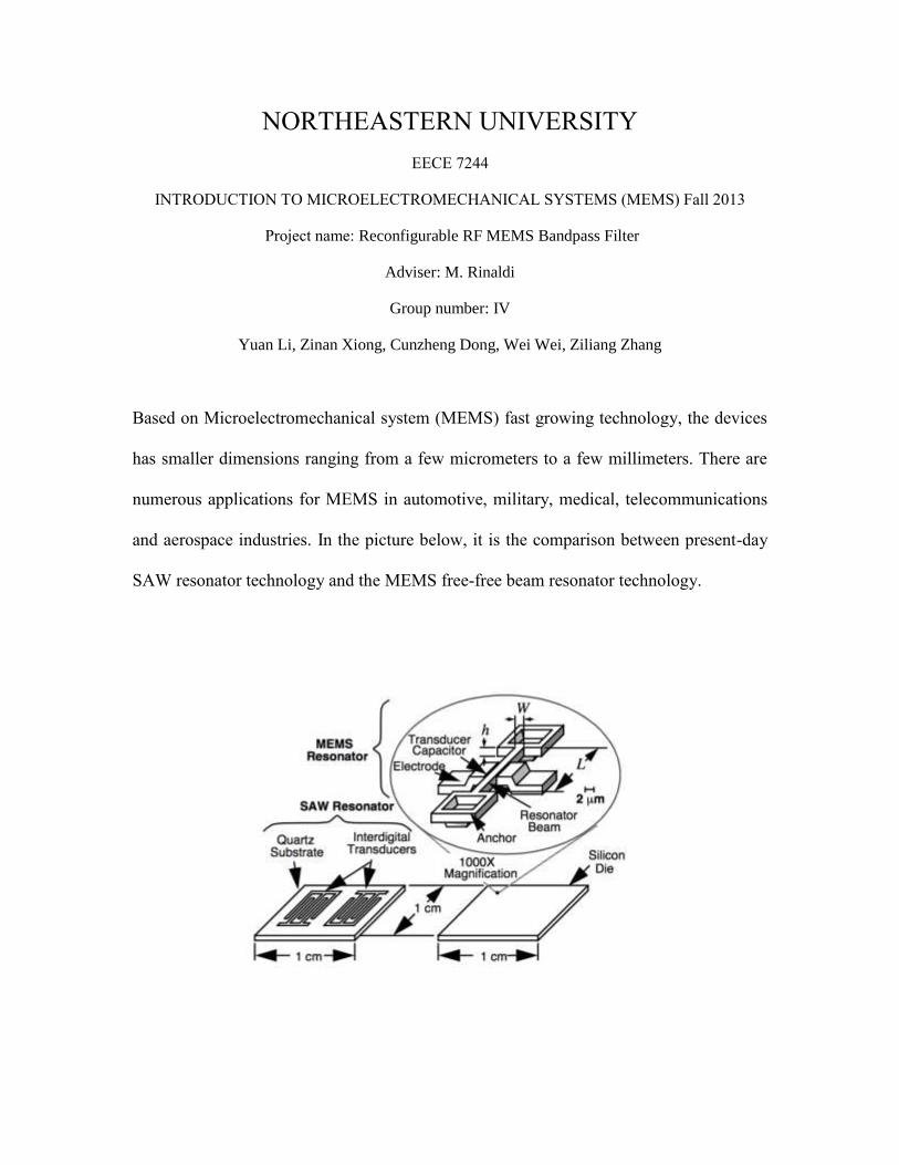
In our design, we consider the range of the radio frequency and we trying design a
bandpass filter which can work on kHz, MHz and also GHz. We use cantilever switch to
change the choice of the filter and in this way to make our device work on the different
frequencies. Because all the knowledge we used in our design is from our class and
lectures, so we just design the filter, which can work on both kHz and MHz. and we still
trying to design the filter which operate on microwave frequencies (1GHz and above). In
the kHz filter design we use the 2nd order comb-driven filter. In the MHz filter design we
use the 2nd order fixed-fixed beam filter. In the figure below its show’s the concept of the
2nd order filter.
Figure 2nd order filter
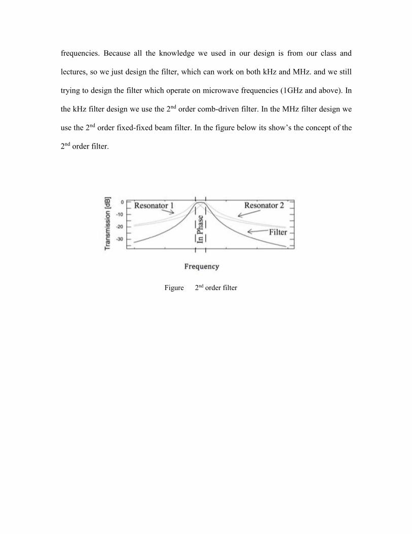
Comb-Driven filter
Our first filter is use comb-Driven model. Two-port, folded-beam, lateral comb-
driven resonator.
Figure 1 shows the overhead view of a two-port, folded-beam, and lateral comb-
driven resonator. The resonator mainly consists of electrostatic comb capacitor,
movable electrode, supporting beam, fixed end, fixed electrode. Movable plate
moves under the electrostatic force generated by the interdigitated comb fingers,
and thus the deformation happens, of the supporting beams. When the structure be
supplied with an AC signal, the movable plate begins to vibrate under both
electrostatic force and elastic force. At a time when the frequency of the drive
voltage is close to the movable comb structure’s nature frequency, oscillation
happens.
Fig. 1 Overhead view of a two-port, folded-beam, and lateral comb-driven resonator
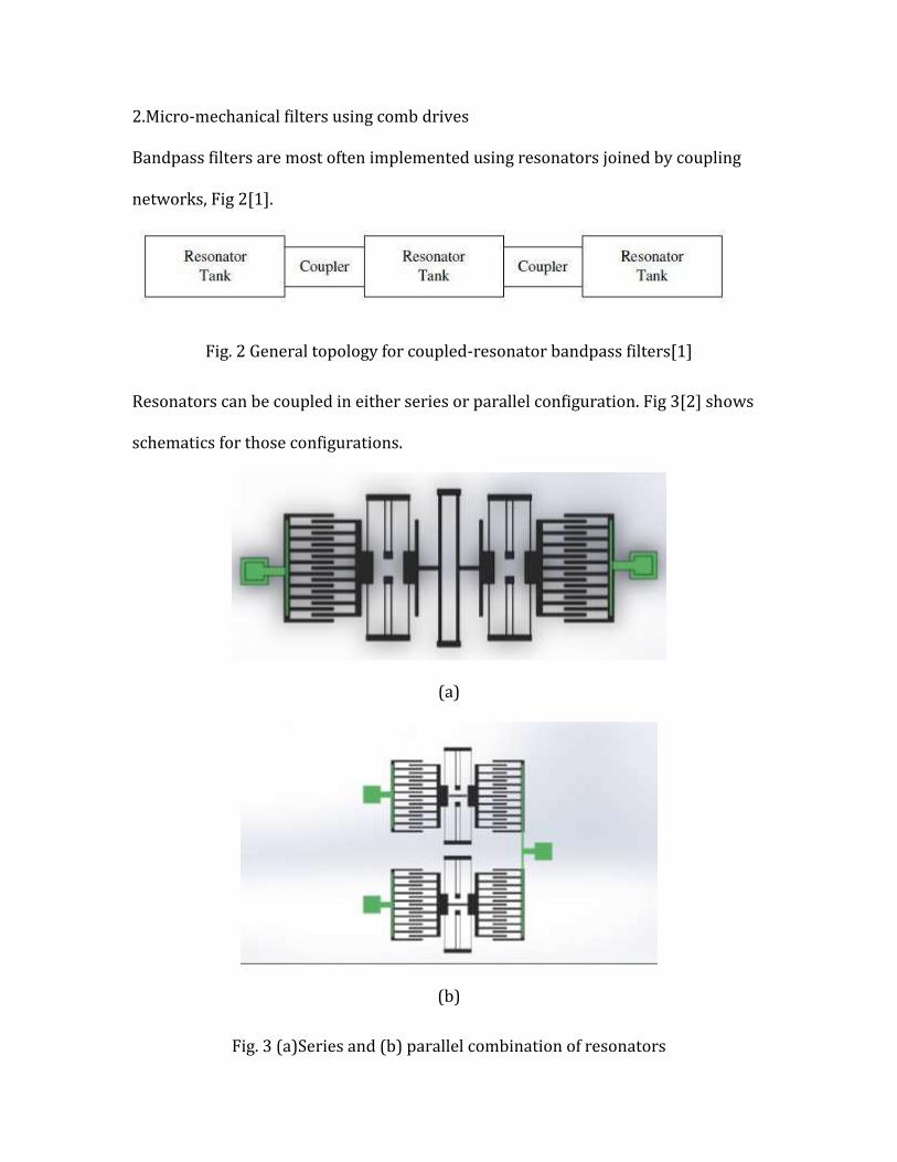
2.Micro-mechanical filters using comb drives
Bandpass filters are most often implemented using resonators joined by coupling
networks, Fig 2[1].
Fig. 2 General topology for coupled-resonator bandpass filters[1]
Resonators can be coupled in either series or parallel configuration. Fig 3[2] shows
schematics for those configurations.
(a)
(b)
Fig. 3 (a)Series and (b) parallel combination of resonators

In the series filter, a square truss coupling spring connects the two resonators. In
the parallel configuration of band pass filter, the input and output terminals of the
resonators are connected in parallel such that the output current are added up[2].
3. The series two-resonator micro filter
In this project of reconfigurable RF MEMS filter, we use the series combination of
two comb-driven resonators to build the first stage of reconfigurable RF filter. The
goal of the center frequency of this filter is about 700 kHz.
Fig. 4 Series two-resonator micro filter
Signals, in the form of current or voltage, are converted by an input
electromechanical transducer into mechanical vibrations at the filter, pass through
the series filter, and are then converted back into electrical signals by an output
electromechanical transducer[3].
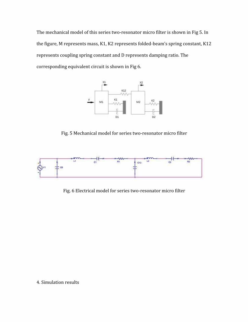
The mechanical model of this series two-resonator micro filter is shown in Fig 5. In
the figure, M represents mass, K1, K2 represents folded-beam’s spring constant, K12
represents coupling spring constant and D represents damping ratio. The
corresponding equivalent circuit is shown in Fig 6.
Fig. 5 Mechanical model for series two-resonator micro filter
Fig. 6 Electrical model for series two-resonator micro filter
4. Simulation results
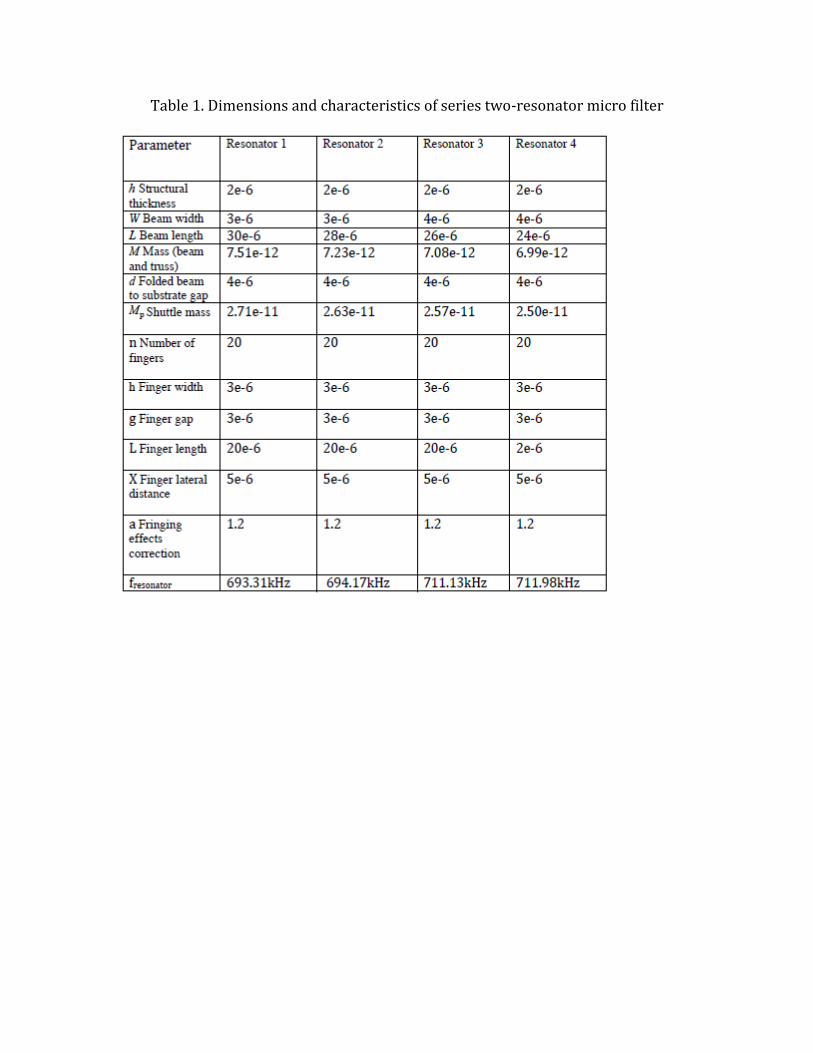
Table 1. Dimensions and characteristics of series two-resonator micro filter

Fixed-Fixed beam filter
In our design, the second resonator and filter we use the Fixed-Fixed beam (FF beam)
filter. It’s also called Clamped-Clamped beam. The picture below is the structure of FF
beam resonator.
In the high frequency range, in order to maximize resonance frequency, based on the
general expression
𝑓0 =1
2𝜋√
𝑘𝑟
𝑚𝑟
The effective resonator spring stiffness 𝑘𝑟 must be maximized, while its effective mass
𝑚𝑟 minimized. The resonator’s frequency on this FF beam depends on many factors, like
structure material properties, stress, and bias-voltage Vp and so on. After consider these
factors while neglecting finite width effects, the expression for resonator frequency can
be written as below:
The electrical equivalent circuit for the resonator in the picture below

The principle of the resonator work is when we put a AC as the Vin at the electrode pad,
the resonator pad (red part in the picture below) will have an attraction force between the
Vin electrode pad and resonator pad, and there will occurs oscillation. The frequency of
this oscillation is the center frequency of this resonator.
Here we need to know, if we don’t put a bias-valtage (Vp) the resonator in an open circuit
condition.
In the table below, it is the parameter of the center frequency f0 equation. Which shows
Yong’s modulus, density of structural material, bias-voltage, the size of the resonator and
so on. For the MEMS resonators, the k is dominate by the anchor step-up and finite
elasticity effects.
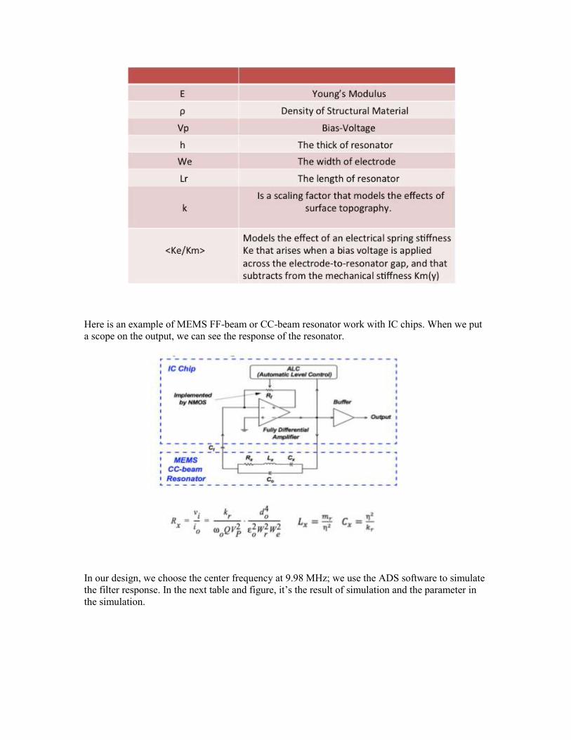
Here is an example of MEMS FF-beam or CC-beam resonator work with IC chips. When we put
a scope on the output, we can see the response of the resonator.
In our design, we choose the center frequency at 9.98 MHz; we use the ADS software to simulate
the filter response. In the next table and figure, it’s the result of simulation and the parameter in
the simulation.

Now we can design the 2nd order filter. The principle of the filter is to connect the two resonators
through a coupling spring in parallel and they will oscillate in a closing frequency. The
structure of the filter is shows on the picture below.
The electrical equivalent circuit is shows here. The green part in the picture is the coupling spring.

The first filter center frequency is 10.04 MHz and the second filter center frequency is 15.29 MHz. The parameter of resonator is shows below.

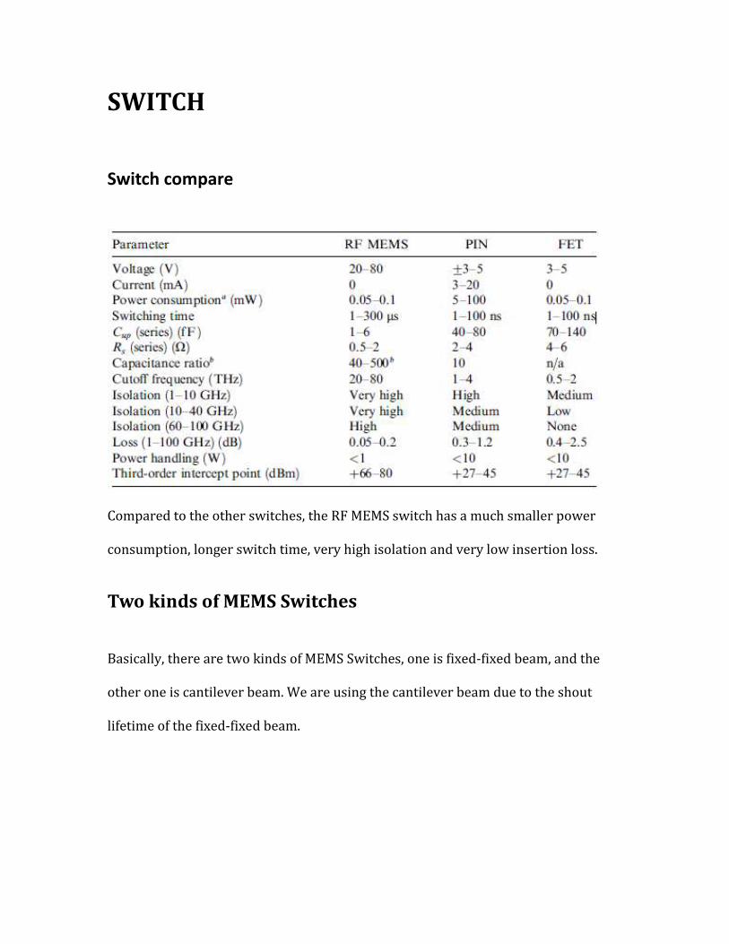
SWITCH
Switch compare
Compared to the other switches, the RF MEMS switch has a much smaller power
consumption, longer switch time, very high isolation and very low insertion loss.
Two kinds of MEMS Switches
Basically, there are two kinds of MEMS Switches, one is fixed-fixed beam, and the
other one is cantilever beam. We are using the cantilever beam due to the shout
lifetime of the fixed-fixed beam.
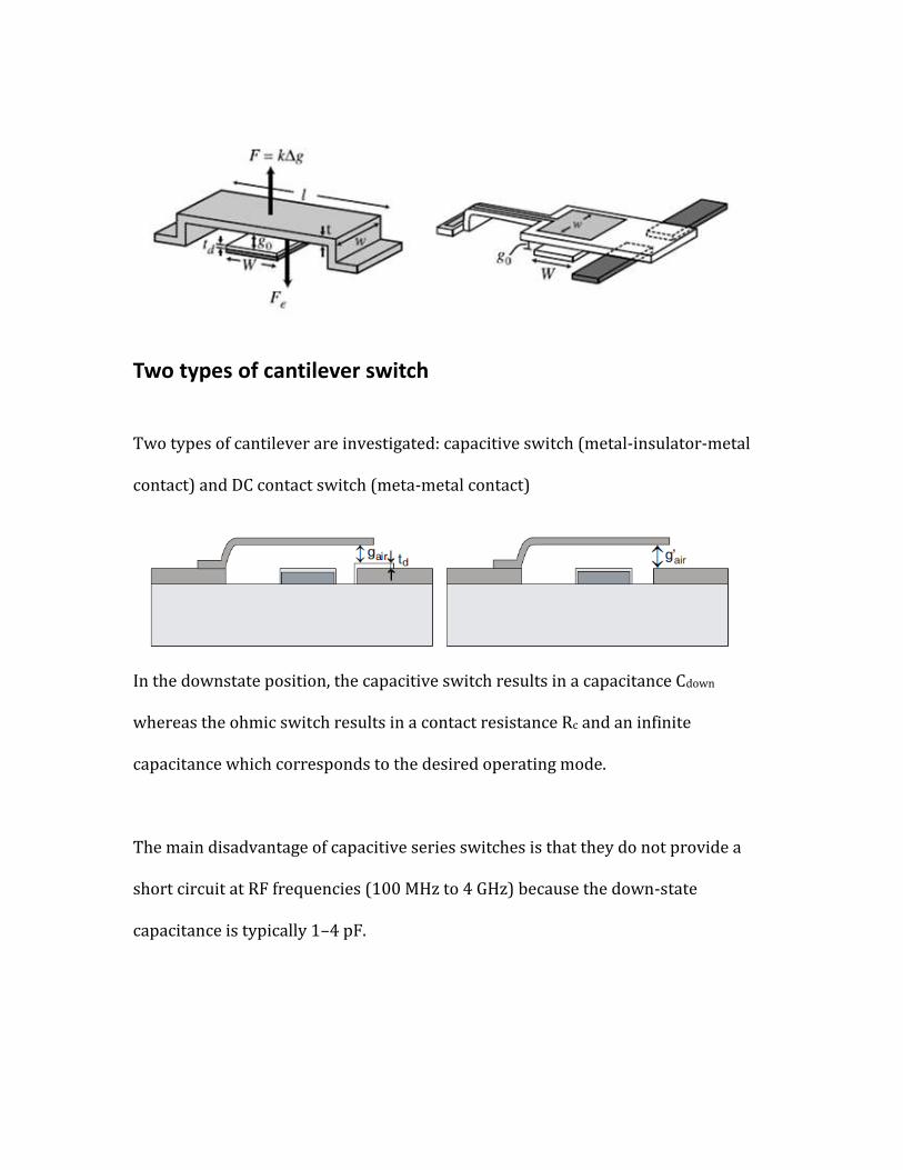
Two types of cantilever switch
Two types of cantilever are investigated: capacitive switch (metal-insulator-metal
contact) and DC contact switch (meta-metal contact)
In the downstate position, the capacitive switch results in a capacitance Cdown
whereas the ohmic switch results in a contact resistance Rc and an infinite
capacitance which corresponds to the desired operating mode.
The main disadvantage of capacitive series switches is that they do not provide a
short circuit at RF frequencies (100 MHz to 4 GHz) because the down-state
capacitance is typically 1–4 pF.

From these observations, the inline DC contact MEMS series switch is the most
suitable for our application.
Cantilever beam switch Topology
Equivalent circuit
Geometric parameters of cantilever
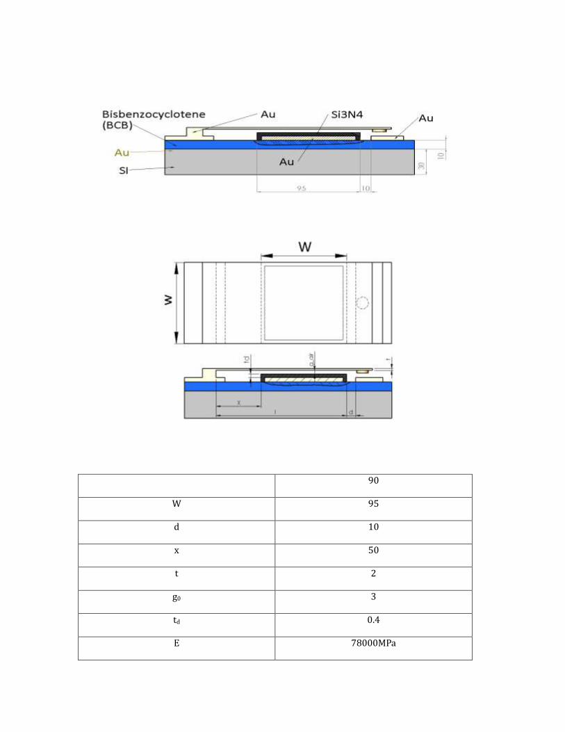
90
W 95
d 10
x 50
t 2
g0 3
td 0.4
E 78000MPa
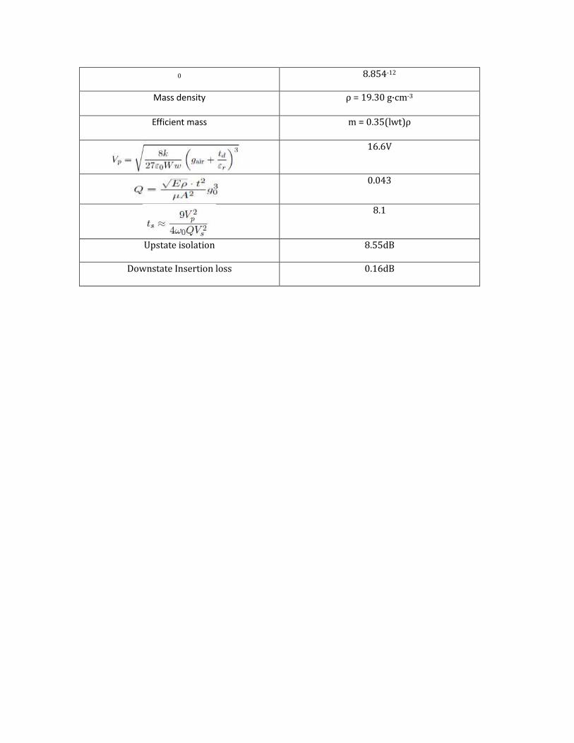
0 8.854-12
Mass density ρ = 19.30 g·cm-3
Efficient mass m = 0.35(lwt)ρ
16.6V
0.043
8.1
Upstate isolation 8.55dB
Downstate Insertion loss 0.16dB


Fabrication process flow
1. The Fabrication process of the switch
Figure the fabrication process flow of RF MEMS switch
The fabrication process of RF MEMS switch composes of eight main steps which are
described as follows:
(1) First the ground plan of microstrip is realized using a Ti/Au seed layer deposited by
evaporation prior to gold electroplating.
(2) The via-holes are then deposited by 20-μm-thick gold electroplating in a thick
photoresist mould.
(3) Next step consists in BCB deposition. A 300A thin film of titanium is first evaporated
in order to improve adhesion of BCB layer on gold. 20-μm-thick BCB layer is then
deposited. The polymer is then hard-cured at 250℃. Next step consists in an oxygen
plasma descuming to eliminate residues left from the BCB deposition.
(4) The microstrip is then elaborated in a similar way as the ground plane metallization.
Nevertheless, at this time Ti/Au evaporation should be realized at 150℃ to enhance
adhesion of gold on BCB layer. The seed layer Ti/Au between lines is then removed by
chemical etching.
(5) Next step is to realize dielectric layer on the electrode. A 500ºA-thick Ti layer is first
evaporated on the electrode to improve adhesion of dielectric layer on gold. The 400 nm-
thick Si3N4 layer is then deposited by plasma-enhanced chemical vapor deposition
(PECVD). The dielectric layer out of the electrode is etched by reactive ion etching (RIE).
(6) Once the dielectric layer is patterned on the electrode, a photoresist mould is
deposited for gap filling and then two sacrificial photoresist layers are elaborated which
form cantilever (growth of anchors and dimples).
(7) Cantilever metallization is deposited by 100 nm-thick gold evaporation followed by
1.9 μm-thick Au electroplating and then gold etching.
(8) The final step consists in releasing the switch. The sacrificial layer is removed using
successive chemicals baths and the structure is dried by CO2 critical point drying system.
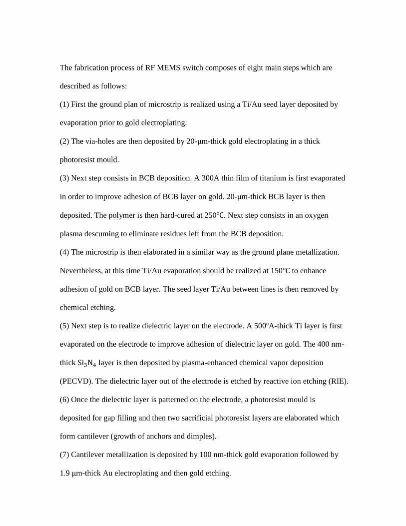
2. The Fabrication process of the fixed-fixed beam filter
Here, patterned phosphorus-doped poly-silicon I/O electrodes and interconnect (3000 Å
thick) are covered by a 1300-Å-thick layer of sacrificial LPCVD silicon dioxide, except
at portions wet-etched to serve as anchors for eventual resonators. A 2- m-thick structural
poly-silicon film is then deposited via LPCVD at 585℃ and made conductive via a POCl
gas doping step. 5000 Å of LPCVD SiO2 then follows to serve first as a diffusion barrier
against dopant loss during a subsequent 1-h 1050℃ stress and dopant distribution anneal,
then as a hard mask during patterning of the structural poly-silicon layer via a chlorine-
based, high-density-plasma reactive ion etch (RIE). Note that throughout the back end of
this process, the sacrificial oxide layer supports the structural poly-silicon material during
deposition, patterning, and annealing, and defines the electrode-to-resonator gap spacing
d0. In the final step of the process, the wafer is dipped into a solution of hydrofluoric acid,
which etches away the sacrificial oxide layer without significantly attacking the poly-
silicon structural material. This leaves the free-standing structure shown in Fig.2 free to
move in several dimensions if necessary. The release etch is followed by extensive
cleaning, including a 10-min dip in a solution of H2SO4 and H2O2 and often a
supercritical CO2 clean, to remove etch by-products and other residuals from the thin
electrode-to-resonator gap.
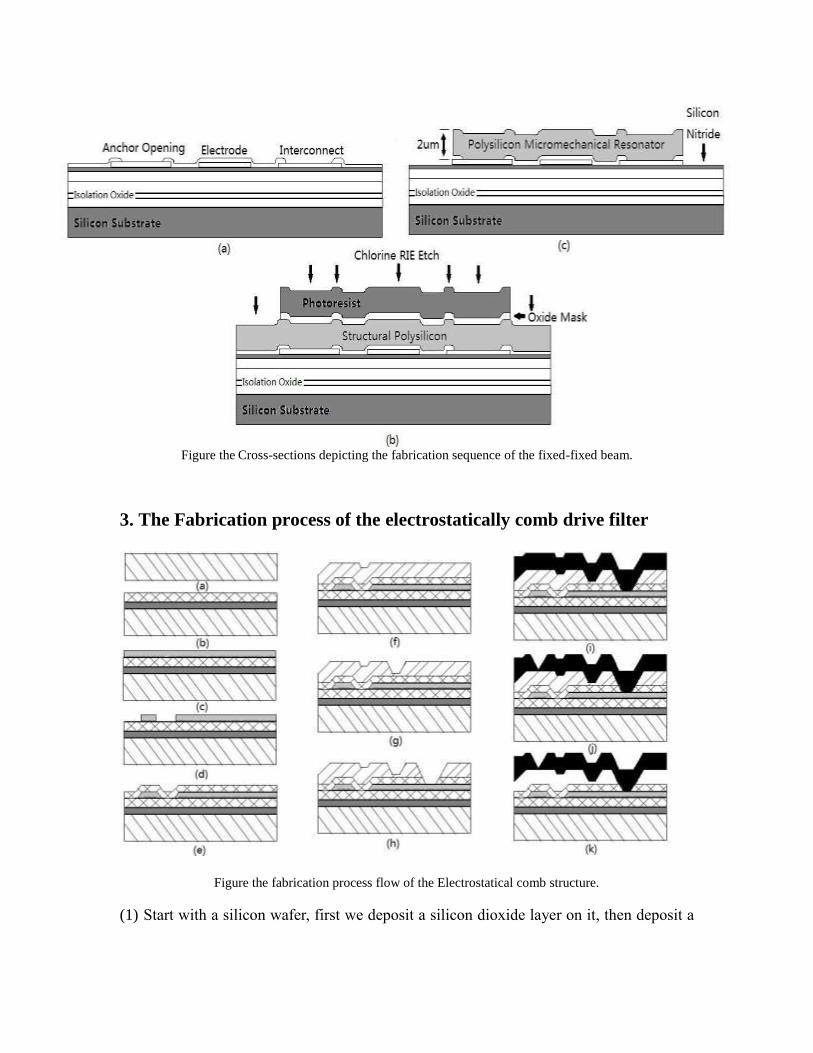
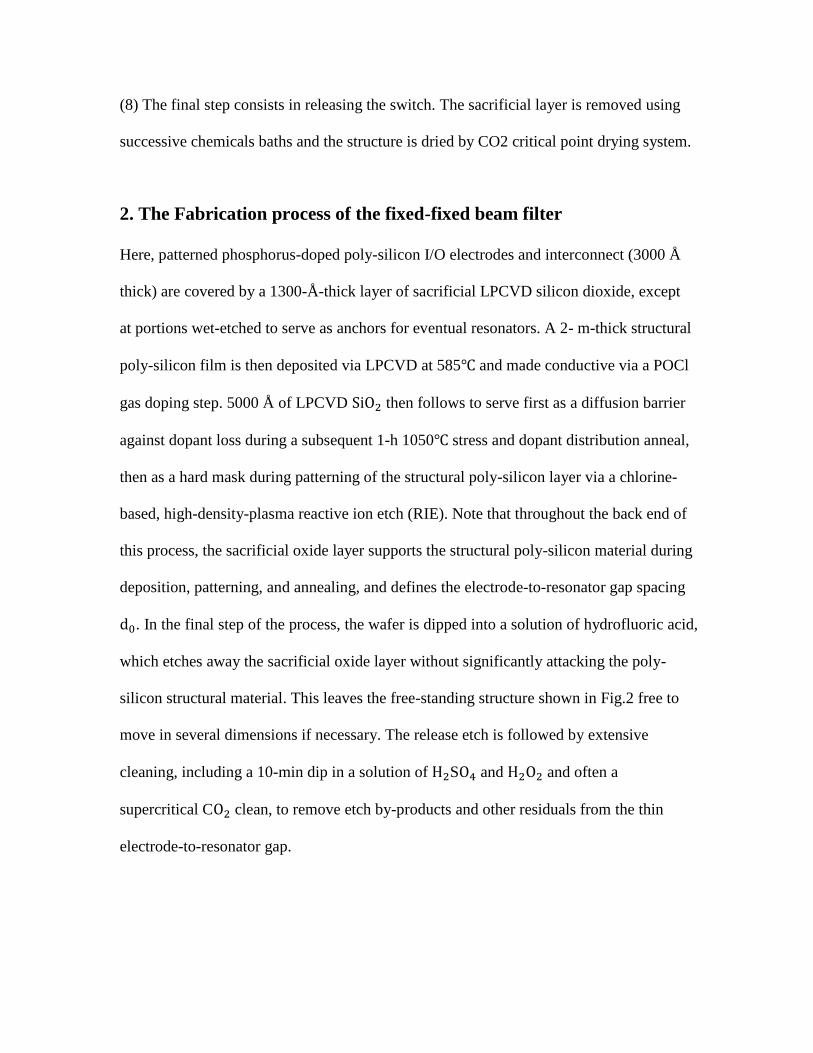
Figure the Cross-sections depicting the fabrication sequence of the fixed-fixed beam.
3. The Fabrication process of the electrostatically comb drive filter
Figure the fabrication process flow of the Electrostatical comb structure.
(1) Start with a silicon wafer, first we deposit a silicon dioxide layer on it, then deposit a
silicon nitride layer on the silicon dioxide layer which both composite as the insulator.
(2) LPCVD a thin layer of poly-silicon onto the insulator and dope it in order to provide
conductance between the mechanism.
(3) Using the mask to perform the first photolithography, retain the figure to form wire
and gauge and other figures.
(4) Make another silicon nitride insulator in case of short-circuited when the conduct
layer might have contacted the poly-silicon.
(5) Deposit a 2-micron-thick sacrifice layer, using the mask to perform the second
photolithography which will prepare for the formation of the bump of suspended
mechanism in order to provide support and reduce adhesion.
(6) Using another mask to perform the third photolithography of the sacrifice layer, carve
the selected figure to form anchor in order to support the poly-silicon structure and
realize the connection between the conduct layer and the poly-silicon layer.
(7) Deposit a 2-micron-thick poly-silicon, using the mask to perform the fourth
photolithography. Retain the figure of moveable comb, foldable beam, and mass bulk.
(8) Finally we use diluted HF solution to get the complete structure.
References
[1] T. M. Vu1, G. Prigent, J. Ruan, and R. Plana, “Design and fabrication of RF-MEMS
switch for V-band reconfigurable application”, Progress In Electromagnetics Research B,
Vol. 39, 301-318, 2012
[2] Frank D. Bannon, III, Student Member, IEEE, John R. Clark, Student Member, IEEE,
and Clark T.-C. Nguyen, Member, IEEE, “High-Q HF Microelectromechanical Filters”,
IEEE JOURNAL OF SOLID-STATE CIRCUITS, VOL. 35, NO. 4, APRIL 2000
[3] Liwei Lin, Roger T. Howe, Fellow, IEEE, and Albert P. Pisano,
“Microelectromechanical Filters for Signal Processing”, JOURNAL OF
MICROELECTROMECHANICAL SYSTEMS, VOL. 7, NO. 3, SEPTEMBER 1998
[4] Md. Fokhrul Islam, Mohd Alauddin Mohd Ali, Burhanuddin Yeop Majlis, "RF
MEMS TUNABLE FILTER USING MICRO FIXED–FIXED BEAM"
[5] Durai Praveen. D, Gautham Muthukumar. S, "RF MEMS Filters"
[6] Elliott R. Brown, "RF-MEMS Switches for Reconfigurable Integrated Circuits"
[7] S. Kanthamani, s. Raju and V. Abhai Kumar, "Design of Low Actuation Voltage RF
MEMS Cantilever Switch"
[8] James Brank, Jamie Yao, Mike Eberly, Andrew Malczewski, Karl Varian,
Charles Goldsmith, "RF MEMS-Based Tunable Filters"
[9] Ai-Qun Liu, "RF MEMS Switches and Integrated Switching Circuits"
[10] Bashar K. Hammad, 2008. “Modeling, Simulation, and Analysis of
Micromechanical Filters Coupled with Capacitive Transducers”. PhD dissertation,
Virginia Polytechnic Institute and State University.
[11] Vijay K. Varadan, K.J Vinoy, K.A. Jose, 2003. “RF MEMS filters and their
applications”. 258-265.