Reconfigurable multi-mode sigma–delta modulator for 4G mobile terminals
13
Reconfigurable multi-mode sigma–delta modulator for 4G mobile terminals Artur Silva a,b , Jorge Guilherme b,c , Nuno Horta a,b, a Instituto Superior Te´cnico, Technical University of Lisbon, Lisbon, Portugal b Instituto de Telecomunicac - o ˜es, Lisbon, Portugal c Escola Superior de Tecnologia de Tomar, Instituto Polite´cnico de Tomar, Tomar, Portugal article info Keywords: Multi-standard Sigma–delta modulator Reconfigurable Analog-to-digital converter abstract A reconfigurable sigma–delta modulator, which is able to support the predictable standards for the fourth generation (4G) of mobile communication systems, is presented in this paper. This modulator was designed to cope with six different communications standards relying on a flexible architecture. Furthermore, the proposed architecture introduces the ability to process concurrently two different signals. The major design issues are outlined and operation modes are detailed. The feasibility of the presented solution is demonstrated using high-level system-level simulations as well as device-level simulations of the modulator implemented with switched capacitor circuits. & 2008 Elsevier B.V. All rights reserved. 1. Introduction The incessant growth on wireless mobile systems poses continuously new challenges to the development of novel solutions, capable to accommodate the new emerging technolo- gies. Over the years, standards for wireless communications systems have constantly being developed in order to achieve higher data rates and at the same time allow the introduction of new services. Permanent technology developments allowed the design of transceivers capable to adjust to more challenging specifications through the generations of cellular systems. 1.1. Standards evolution on mobile terminals The first generation of cellular systems, which was based on analog voice modulation, appeared in the 1980s. Several standards operated at different parts of the globe, as nordic mobile telephone (NMT) in Europe or advanced mobile phone system (AMPS) in North America. The succeeding generation, 2G, was introduced 10 years later replacing the later voice analog modulation by a digital one. Like 1G, different standards appeared worldwide, although global system for mobile (GSM) commu- nications rapidly spread over world, becoming the major mobile phone standard. During 2G, data rates were progressively increased, up to 384 kbps, with the development of GSM, by introducing General Packet Radio Service (GPRS) and enhanced data rate for GSM evolution (EDGE) systems. Previous generations supported mainly voice applications, while 3G provided a wider range of services at higher data rates (about 5 Mbps) through the use of the access scheme wide-band code division multiple access (WCDMA), for instance. The limited success of 3G associated with new emerging standards and the upcoming of a new generation every decade forced the development of fourth generation (4G) [1]. Therefore, 4G is predicted to be implemented near 2010–2015 with data rates up to 100 Mbps envisaging a new concept of mobility and cooperative services. Although it is not fully defined yet, 4G is expected to be a convergence platform, offering a plethora of new heterogeneous services. Besides the integration of former stan- dards as GSM, WCDMA and Bluetooth, 4G will incorporate high- speed access technologies, such as wireless local area network (WLAN) and wireless metropolitan area network (WMAN), represented by IEEE 802.11a/b/g and WiMAX. This standard’s convergence is depicted in Fig. 1 . 1.2. Multi-standard receivers Handheld devices are expected to cope with diverse specifica- tions, resulting from the implementation of a large variety of standards in 4G. The need to support several standards in the same handheld device, associated with the power consumption and area restrictions, created the necessity to develop a portable, power efficient, integrated solution. This would require multi- mode user terminals that are able to adapt themselves to the user’s requirements [2–4]. The most straightforward solution is the implementation of several front-end receivers, contradicting the objectives of area and power minimization in mobile devices. To overcome these limitations the multi-standard solution was developed. Multi-standard receivers lead to flexible, reconfigur- able solutions, controlled by software, that are adjusted to the ARTICLE IN PRESS Contents lists available at ScienceDirect journal homepage: www.elsevier.com/locate/vlsi INTEGRATION, the VLSI journal 0167-9260/$ - see front matter & 2008 Elsevier B.V. All rights reserved. doi:10.1016/j.vlsi.2008.07.004 Corresponding author at: Instituto de Telecomunicac - o ˜es, Lisbon, Portugal. E-mail address: [email protected] (N. Horta). INTEGRATION, the VLSI journal 42 (2009) 34–46
-
Upload
artur-silva -
Category
Documents
-
view
213 -
download
0
Transcript of Reconfigurable multi-mode sigma–delta modulator for 4G mobile terminals

ARTICLE IN PRESS
INTEGRATION, the VLSI journal 42 (2009) 34–46
Contents lists available at ScienceDirect
INTEGRATION, the VLSI journal
0167-92
doi:10.1
� Corr
E-m
journal homepage: www.elsevier.com/locate/vlsi
Reconfigurable multi-mode sigma–delta modulator for 4G mobile terminals
Artur Silva a,b, Jorge Guilherme b,c, Nuno Horta a,b,�
a Instituto Superior Tecnico, Technical University of Lisbon, Lisbon, Portugalb Instituto de Telecomunicac- oes, Lisbon, Portugalc Escola Superior de Tecnologia de Tomar, Instituto Politecnico de Tomar, Tomar, Portugal
a r t i c l e i n f o
Keywords:
Multi-standard
Sigma–delta modulator
Reconfigurable
Analog-to-digital converter
60/$ - see front matter & 2008 Elsevier B.V. A
016/j.vlsi.2008.07.004
esponding author at: Instituto de Telecomun
ail address: [email protected] (N. Horta).
a b s t r a c t
A reconfigurable sigma–delta modulator, which is able to support the predictable standards for the
fourth generation (4G) of mobile communication systems, is presented in this paper. This modulator
was designed to cope with six different communications standards relying on a flexible architecture.
Furthermore, the proposed architecture introduces the ability to process concurrently two different
signals. The major design issues are outlined and operation modes are detailed. The feasibility of the
presented solution is demonstrated using high-level system-level simulations as well as device-level
simulations of the modulator implemented with switched capacitor circuits.
& 2008 Elsevier B.V. All rights reserved.
1. Introduction
The incessant growth on wireless mobile systems posescontinuously new challenges to the development of novelsolutions, capable to accommodate the new emerging technolo-gies. Over the years, standards for wireless communicationssystems have constantly being developed in order to achievehigher data rates and at the same time allow the introduction ofnew services. Permanent technology developments allowed thedesign of transceivers capable to adjust to more challengingspecifications through the generations of cellular systems.
1.1. Standards evolution on mobile terminals
The first generation of cellular systems, which was based onanalog voice modulation, appeared in the 1980s. Several standardsoperated at different parts of the globe, as nordic mobiletelephone (NMT) in Europe or advanced mobile phone system(AMPS) in North America. The succeeding generation, 2G, wasintroduced 10 years later replacing the later voice analogmodulation by a digital one. Like 1G, different standards appearedworldwide, although global system for mobile (GSM) commu-nications rapidly spread over world, becoming the major mobilephone standard. During 2G, data rates were progressivelyincreased, up to 384 kbps, with the development of GSM, byintroducing General Packet Radio Service (GPRS) and enhanceddata rate for GSM evolution (EDGE) systems. Previous generationssupported mainly voice applications, while 3G provided a wider
ll rights reserved.
icac- oes, Lisbon, Portugal.
range of services at higher data rates (about 5 Mbps) through theuse of the access scheme wide-band code division multiple access(WCDMA), for instance.
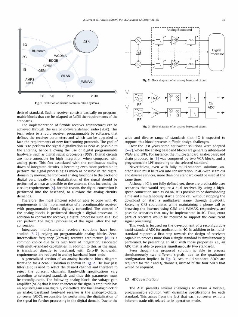
The limited success of 3G associated with new emergingstandards and the upcoming of a new generation every decadeforced the development of fourth generation (4G) [1]. Therefore,4G is predicted to be implemented near 2010–2015 with datarates up to 100 Mbps envisaging a new concept of mobility andcooperative services. Although it is not fully defined yet, 4G isexpected to be a convergence platform, offering a plethora of newheterogeneous services. Besides the integration of former stan-dards as GSM, WCDMA and Bluetooth, 4G will incorporate high-speed access technologies, such as wireless local area network(WLAN) and wireless metropolitan area network (WMAN),represented by IEEE 802.11a/b/g and WiMAX. This standard’sconvergence is depicted in Fig. 1.
1.2. Multi-standard receivers
Handheld devices are expected to cope with diverse specifica-tions, resulting from the implementation of a large variety ofstandards in 4G. The need to support several standards in thesame handheld device, associated with the power consumptionand area restrictions, created the necessity to develop a portable,power efficient, integrated solution. This would require multi-mode user terminals that are able to adapt themselves to theuser’s requirements [2–4]. The most straightforward solution isthe implementation of several front-end receivers, contradictingthe objectives of area and power minimization in mobile devices.To overcome these limitations the multi-standard solution wasdeveloped. Multi-standard receivers lead to flexible, reconfigur-able solutions, controlled by software, that are adjusted to the
ARTICLE IN PRESS
WLAN
Bluetooth
2010
4G
WiMAX
1G
2G
3G
AMPSNMT
‘80
WCDMA
GSMGPRS
EDGE
‘90 2000
Fig. 1. Evolution of mobile communication systems.
PGA ADC
090
PGA ADC
DigitalProcessor
Analog Baseband
Fig. 2. Block diagram of an analog baseband circuit.
ΣΔADC
LNA
RFI
RF
LNA
Q
I Q
Fig. 3. Block diagram of an analog baseband circuit.
A. Silva et al. / INTEGRATION, the VLSI journal 42 (2009) 34–46 35
desired standard. Such a receiver consists basically on program-mable blocks that can be adapted to fulfill the requirements of thestandards.
The implementation of flexible receiver architectures can beachieved through the use of software defined radio (SDR). Thisterm refers to a radio receiver, programmable by software, thatdefines the receiver parameters and which can be upgraded toface the requirements of new forthcoming protocols. The goal ofSDR is to perform the signal digitalization as near as possible tothe antenna, hence allowing the use of digital programmablehardware, such as digital signal processors (DSPs). Digital circuitsare more amenable for high integration when compared withanalog parts. This fact associated with the continuous scalingdown of integrated circuits, is becoming even more preferable toperform the signal processing as much as possible in the digitaldomain by moving the front-end analog functions to the back-enddigital part. Ideally, the digitalization of the signal should beperformed as near as possible to the antenna, thus increasing thecircuits requirements [4]. For this reason, the digital conversion isperformed into the baseband, to alleviate the analog circuits’demands.
Therefore, the most efficient solution able to cope with 4Grequirements is the implementation of a reconfigurable receiver,with programmable blocks digitally controlled. The control ofthe analog blocks is performed through a digital processor. Inaddition to control the receiver, a digital processor such as a DSPcan perform the digital processing of the signal after the A/Dconversion.
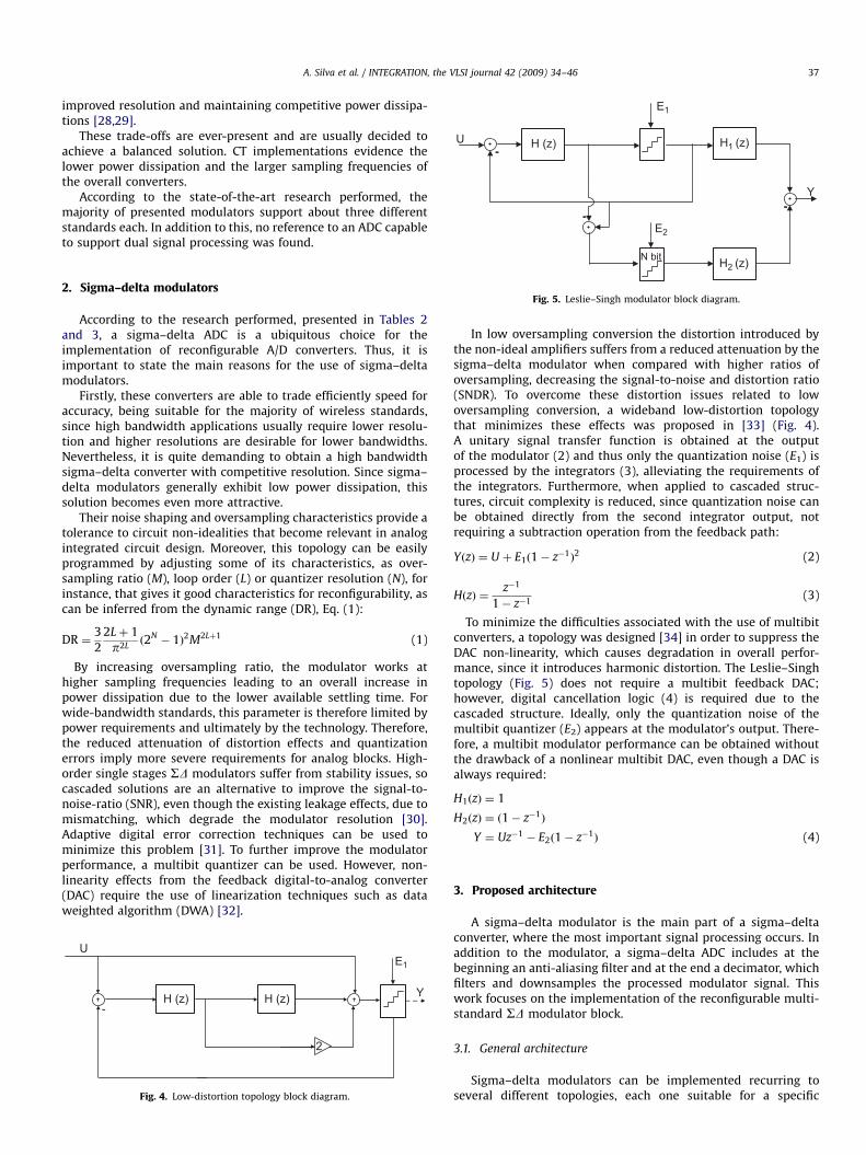
Integrated multi-standard receivers solutions have beenstudied [5–7], relying on programmable analog blocks. Zero-intermediate frequency (Zero-IF) receiver architecture [8] is acommon choice due to its high level of integration, associatedwith multi-standard capabilities. In addition to this, as the signalis translated directly to baseband, with Zero-IF, bandwidthrequirements are reduced in analog baseband front-ends.
A generalized version of an analog baseband block diagramfront-end for a Zero-IF solution is shown in Fig. 2. The low passfilter (LPF) is used to select the desired channel and therefore toreject the adjacent channels. Bandwidth specifications varyaccording to selected standards and thus this parameter mustbe reconfigurable. The following analog block, the voltage gainamplifier (VGA) that is used to increase the signal’s amplitude hasan adjusted gain also digitally controlled. The final analog block ofan analog baseband front-end receiver is the analog-to-digitalconverter (ADC), responsible for performing the digitalization ofthe signal for further processing in the digital domain. Due to the
wide and diverse range of standards that 4G is expected tosupport, this block presents difficult design challenges.
Over the last years some equivalent solutions were adopted[5–7], where the analog baseband blocks are generally interleavedVGAs and LPFs. For instance, the multi-standard analog basebandchain proposed in [7] was composed by two VGA blocks and aprogrammable LPF according to the selected standard.
Nevertheless, even with fully multi-standard solutions, an-other issue must be taken into consideration. In 4G with seamlessand diverse services, more than one standard could be used at thesame time.
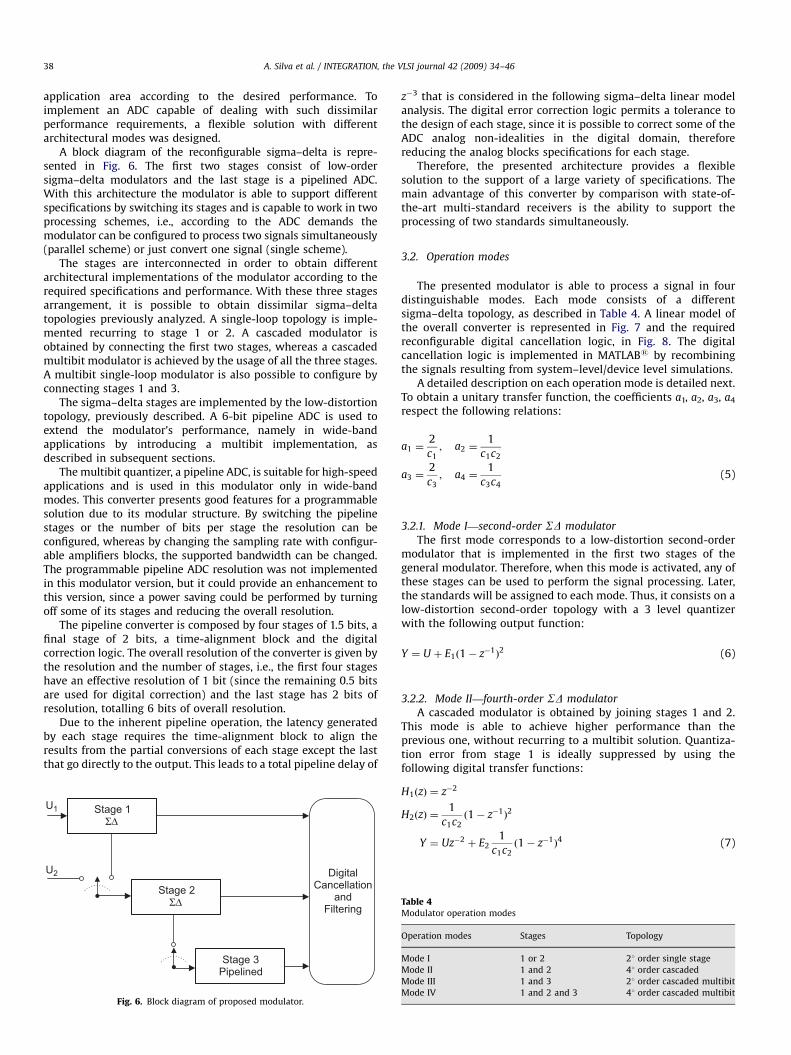
Although 4G is not fully defined yet, there are predictable userscenarios that would require a dual receiver. By using a high-speed connection such as WLAN, it is possible to be downloadinga file and simultaneously start a phone call without stopping thedownload or start a multiplayer game through Bluetooth.Receiving GPS coordinates while maintaining a phone call orbrowsing the internet using GSM and WiMAX, respectively, arepossible scenarios that may be implemented in 4G. Thus, extraparallel receivers would be required to support the concurrentsignal processing.
This work is focused on the development of a reconfigurablemulti-standard ADC for application in 4G. In addition to its multi-standard support, a first step towards the design of receiverscapable to process more than a single standard is simultaneouslyperformed, by presenting an ADC with those properties, i.e., anADC that is able to process simultaneously two standards.
Even though the proposed solution is able to processsimultaneously two different signals, due to the quadratureconfiguration implicit in Fig. 3, two multi-standard ADCs arerequired for the I and Q channels, instead of the four ADCs thatwould be required.
1.3. ADC specifications
The ADC presents several challenges to obtain a flexible,programmable solution with dissimilar specifications for eachstandard. This arises from the fact that each converter exhibitsinherent trade-offs related to its operation mode.

ARTICLE IN PRESS
A. Silva et al. / INTEGRATION, the VLSI journal 42 (2009) 34–4636
A detailed analysis on the overall receiver chain, determiningthe impact of interferers and establishing the specifications foreach block is beyond the scope of this work. Therefore, a researchon ADC specifications was performed, based on several publica-tions on this area [9–27], where the ADC specifications for eachstandard were established, Table 1.
1.4. State-of-the-art
Reusability is an essential key in the development ofreconfigurable A/D converters, since power consumption and arearequirements are a major trend in multi-standard receivers, as
Table 1Wireless communications standards ADC specs
Standard Frequency bands
(MHz)
Channel bandwidth
(MHz)
ENOBa
(bits)
GSM 890–915 0.2 12–14
935–960
Bluetooth 2400–2483,5 1 10–13
GPS 1575,42 2 10
WCDMA 1920–1980 3.84 9–12
2110–2170
WLAN 2400–2483,5 22 8–14
WiMAX 2000–11000 20 7–11
a Effective number of bits.
Table 2State-of-the-art multi-standard A/D converters performance summary (protoype)
Reference
year
Wireless standards ADC Results
DR (dB)
[9] 2001 GSM/UMTS DT 31 order SD 86/54
[10] 2002 GSM/WCDMA DT 21 order SD 79/50
[11] 2003 WCDMA/GPRS DT MASH 2-1 70/82
[12] 2003 GSM/CDMA2000/UMTS CT 51 order SD –
[13] 2003 WCDMA/GSM DT 21 order SD –
[14] 2004 802.11b/Bluetooth Time-interleaved
pipelined
–
[15] 2005 GSM/WCDMA DT 31 order SD 76/55
[16] 2005 GSM/WCDMA/WLAN CT Leslie–Singh –
[17] 2006 CDMA2000/WCDMA DT 21 order SD 76/68
[18] 2007 EDGE/UMTS/WLAN DT 41 order SD 88/79/67
[19] 2007 EDGE/CDMA/UMTS DT/CT 51 order SD 88/82/73
[20] 2007 GSM/Bluetooth/WLAN CT 51 order SD 82/75/52
[21] 2007 GSM/Bluetooth/WCDMA DT MASH 2-1-1 86.7/81/63.3
Table 3State-of-the-art multi-standard A/D converters performance summary (simulation leve
Reference
year
Wireless standards ADC Results
DR (dB)
[22] 2004 GSM/UMTS/WLANa DT MASH 2-2-1 103/82/66
[23] 2004 WCDMA/GSM/Bluetooth MASH 2-2, 5-5 bit –
[24] 2004 GSM/WCDMA DT MASH 2-2, 1-4 bit –
[25] 2006 GSM/WCDMA/WLAN DT31order SD 4bit –
[26] 2006 GSM/WCDMA/WLAN/
WiMAX
DT MASH 2-2, 4-4 bit –
[27] 2006 GSM/BLUETOOTH/UMTS/
WLAN
DT MASH 2-1-1 85/72/62/59
stated earlier. Thus, it is vital to the converter to be able to scaleeasily through resolution and bandwidth.
Focusing on reconfigurable converters for application in multi-standard receivers, a state-of-the-art research is presented. Ashave been seen before, plenty of standards are expected to beimplemented in mobile devices on 4G. Therefore, severalpublications have been presented through recent years regardingthis issue, thus emphasizing the importance of multi-standardreceivers. However, the majority of these publications focused onlow-medium bandwidth standards [9–13,15,17,19,21,23,24], sup-porting essentially GSM and WCDMA standards. Recently, newconverters were introduced in order to improve the bandwidthand therefore to be able to cope with WLAN requirements[14,16,18,20,22,25–27].
The performance summary of recently published reconfigur-able multi-standard A/D converters is presented in Tables 2 and 3.The former table groups the proposed converters that have beensubmitted to fabrication, while the latter contains results fromsimulations. In the tables the circuit implementation of eachpresented solution is indicated, namely continuous-time (CT) anddiscrete-time (DT).
From the tables analysis it is evident that WLAN and WiMAXstandards achieve the highest power consumptions. The exceptionis a recent publication [20] based on a CT implementation, wherethe stated power dissipation is closer to the other standards,even though the achieved performance is comparatively lower.Nevertheless, there are implementations in CT circuits with
Max.
sampling
frequency
(MHz)
Technology Power (mW) Area
(mm2)
SNDR (dB)
72/52 184.3 0.25mm 2.5 V 8/8 0.36
75/49 46 0.13mm 1.5 V 2.4/2.9 0.2
64/81 39 0.13mm 1.2 V 4.3/2.4 0.2
92/83/74 153.6 0.18mm 1.8 V 3.8/4.1/4.5 0.18
70/81 46 0.18mm 2.7 V 50 1.4
60/64 44 0.25mm 2.5 V 20.2/14.8 2.1
– 40 0.18mm 1.8 V 4/4 0.7
70/60/58 480 0.18mm 15/15/37 0.9
71/65 61 0.13mm 2.8 V 10/10 0.42
85/77/63 240 0.13mm 1.2 V 2.9/7.4/20.5 0.4
– 153.6 65 nm 2.5 V 2.6/3.1/3.7 0.125
- 400 90 nm 1.2 V 1.44/3.6/6.6 –
74/68.4/52.8 80 0.13mm 3.3 V 11/10.5/24.8 1.37
l)
Max.
sampling
frequency
(MHz)
Type of simulation Power (mW)
SNDR (dB)
101/82/69 320 Device level 0.35mm 3.3 V 40
60/70/53 48 Device level 0.18mm 1.8 V 11/5.8/5
83/75 64 Device level 0.18mm 1.8 V –
96/77/54 160 Device level 0.18mm 1.8 V 18/23/39
83/75/63/63 160 Device level 0.18mm 1.8 V 8.3/17.8/42/42
– 200 Device level 0.35mm 2.2 V 4.6/5.5/7.4/18.9
ARTICLE IN PRESS
- H (z)
-
E1
E2
H1 (z)
-Y
U
A. Silva et al. / INTEGRATION, the VLSI journal 42 (2009) 34–46 37
improved resolution and maintaining competitive power dissipa-tions [28,29].
These trade-offs are ever-present and are usually decided toachieve a balanced solution. CT implementations evidence thelower power dissipation and the larger sampling frequencies ofthe overall converters.
According to the state-of-the-art research performed, themajority of presented modulators support about three differentstandards each. In addition to this, no reference to an ADC capableto support dual signal processing was found.
H2 (z)N bit
Fig. 5. Leslie–Singh modulator block diagram.
2. Sigma–delta modulatorsAccording to the research performed, presented in Tables 2and 3, a sigma–delta ADC is a ubiquitous choice for theimplementation of reconfigurable A/D converters. Thus, it isimportant to state the main reasons for the use of sigma–deltamodulators.
Firstly, these converters are able to trade efficiently speed foraccuracy, being suitable for the majority of wireless standards,since high bandwidth applications usually require lower resolu-tion and higher resolutions are desirable for lower bandwidths.Nevertheless, it is quite demanding to obtain a high bandwidthsigma–delta converter with competitive resolution. Since sigma–delta modulators generally exhibit low power dissipation, thissolution becomes even more attractive.
Their noise shaping and oversampling characteristics provide atolerance to circuit non-idealities that become relevant in analogintegrated circuit design. Moreover, this topology can be easilyprogrammed by adjusting some of its characteristics, as over-sampling ratio (M), loop order (L) or quantizer resolution (N), forinstance, that gives it good characteristics for reconfigurability, ascan be inferred from the dynamic range (DR), Eq. (1):
DR ¼3
2
2Lþ 1
p2Lð2N� 1Þ2M2Lþ1 (1)
By increasing oversampling ratio, the modulator works athigher sampling frequencies leading to an overall increase inpower dissipation due to the lower available settling time. Forwide-bandwidth standards, this parameter is therefore limited bypower requirements and ultimately by the technology. Therefore,the reduced attenuation of distortion effects and quantizationerrors imply more severe requirements for analog blocks. High-order single stages SD modulators suffer from stability issues, socascaded solutions are an alternative to improve the signal-to-noise-ratio (SNR), even though the existing leakage effects, due tomismatching, which degrade the modulator resolution [30].Adaptive digital error correction techniques can be used tominimize this problem [31]. To further improve the modulatorperformance, a multibit quantizer can be used. However, non-linearity effects from the feedback digital-to-analog converter(DAC) require the use of linearization techniques such as dataweighted algorithm (DWA) [32].
H (z) H (z)-
U
Y
E1
2
Fig. 4. Low-distortion topology block diagram.
In low oversampling conversion the distortion introduced bythe non-ideal amplifiers suffers from a reduced attenuation by thesigma–delta modulator when compared with higher ratios ofoversampling, decreasing the signal-to-noise and distortion ratio(SNDR). To overcome these distortion issues related to lowoversampling conversion, a wideband low-distortion topologythat minimizes these effects was proposed in [33] (Fig. 4).A unitary signal transfer function is obtained at the outputof the modulator (2) and thus only the quantization noise (E1) isprocessed by the integrators (3), alleviating the requirements ofthe integrators. Furthermore, when applied to cascaded struc-tures, circuit complexity is reduced, since quantization noise canbe obtained directly from the second integrator output, notrequiring a subtraction operation from the feedback path:
YðzÞ ¼ U þ E1ð1� z�1Þ2 (2)
HðzÞ ¼z�1
1� z�1(3)
To minimize the difficulties associated with the use of multibitconverters, a topology was designed [34] in order to suppress theDAC non-linearity, which causes degradation in overall perfor-mance, since it introduces harmonic distortion. The Leslie–Singhtopology (Fig. 5) does not require a multibit feedback DAC;however, digital cancellation logic (4) is required due to thecascaded structure. Ideally, only the quantization noise of themultibit quantizer (E2) appears at the modulator’s output. There-fore, a multibit modulator performance can be obtained withoutthe drawback of a nonlinear multibit DAC, even though a DAC isalways required:
H1ðzÞ ¼ 1
H2ðzÞ ¼ ð1� z�1Þ
Y ¼ Uz�1 � E2ð1� z�1Þ (4)
3. Proposed architecture
A sigma–delta modulator is the main part of a sigma–deltaconverter, where the most important signal processing occurs. Inaddition to the modulator, a sigma–delta ADC includes at thebeginning an anti-aliasing filter and at the end a decimator, whichfilters and downsamples the processed modulator signal. Thiswork focuses on the implementation of the reconfigurable multi-standard SD modulator block.
3.1. General architecture
Sigma–delta modulators can be implemented recurring toseveral different topologies, each one suitable for a specific
ARTICLE IN PRESS
A. Silva et al. / INTEGRATION, the VLSI journal 42 (2009) 34–4638
application area according to the desired performance. Toimplement an ADC capable of dealing with such dissimilarperformance requirements, a flexible solution with differentarchitectural modes was designed.
A block diagram of the reconfigurable sigma–delta is repre-sented in Fig. 6. The first two stages consist of low-ordersigma–delta modulators and the last stage is a pipelined ADC.With this architecture the modulator is able to support differentspecifications by switching its stages and is capable to work in twoprocessing schemes, i.e., according to the ADC demands themodulator can be configured to process two signals simultaneously(parallel scheme) or just convert one signal (single scheme).
The stages are interconnected in order to obtain differentarchitectural implementations of the modulator according to therequired specifications and performance. With these three stagesarrangement, it is possible to obtain dissimilar sigma–deltatopologies previously analyzed. A single-loop topology is imple-mented recurring to stage 1 or 2. A cascaded modulator isobtained by connecting the first two stages, whereas a cascadedmultibit modulator is achieved by the usage of all the three stages.A multibit single-loop modulator is also possible to configure byconnecting stages 1 and 3.
The sigma–delta stages are implemented by the low-distortiontopology, previously described. A 6-bit pipeline ADC is used toextend the modulator’s performance, namely in wide-bandapplications by introducing a multibit implementation, asdescribed in subsequent sections.
The multibit quantizer, a pipeline ADC, is suitable for high-speedapplications and is used in this modulator only in wide-bandmodes. This converter presents good features for a programmablesolution due to its modular structure. By switching the pipelinestages or the number of bits per stage the resolution can beconfigured, whereas by changing the sampling rate with configur-able amplifiers blocks, the supported bandwidth can be changed.The programmable pipeline ADC resolution was not implementedin this modulator version, but it could provide an enhancement tothis version, since a power saving could be performed by turningoff some of its stages and reducing the overall resolution.
The pipeline converter is composed by four stages of 1.5 bits, afinal stage of 2 bits, a time-alignment block and the digitalcorrection logic. The overall resolution of the converter is given bythe resolution and the number of stages, i.e., the first four stageshave an effective resolution of 1 bit (since the remaining 0.5 bitsare used for digital correction) and the last stage has 2 bits ofresolution, totalling 6 bits of overall resolution.
Due to the inherent pipeline operation, the latency generatedby each stage requires the time-alignment block to align theresults from the partial conversions of each stage except the lastthat go directly to the output. This leads to a total pipeline delay of
Stage 1ΣΔ
Stage 2ΣΔ
Stage 3Pipelined
DigitalCancellation
andFiltering
U2
U1
Fig. 6. Block diagram of proposed modulator.
z�3 that is considered in the following sigma–delta linear modelanalysis. The digital error correction logic permits a tolerance tothe design of each stage, since it is possible to correct some of theADC analog non-idealities in the digital domain, thereforereducing the analog blocks specifications for each stage.
Therefore, the presented architecture provides a flexiblesolution to the support of a large variety of specifications. Themain advantage of this converter by comparison with state-of-the-art multi-standard receivers is the ability to support theprocessing of two standards simultaneously.
3.2. Operation modes
The presented modulator is able to process a signal in fourdistinguishable modes. Each mode consists of a differentsigma–delta topology, as described in Table 4. A linear model ofthe overall converter is represented in Fig. 7 and the requiredreconfigurable digital cancellation logic, in Fig. 8. The digitalcancellation logic is implemented in MATLABs by recombiningthe signals resulting from system–level/device level simulations.
A detailed description on each operation mode is detailed next.To obtain a unitary transfer function, the coefficients a1, a2, a3, a4
respect the following relations:
a1 ¼2
c1; a2 ¼
1
c1c2
a3 ¼2
c3; a4 ¼
1
c3c4(5)
3.2.1. Mode I—second-order SD modulator
The first mode corresponds to a low-distortion second-ordermodulator that is implemented in the first two stages of thegeneral modulator. Therefore, when this mode is activated, any ofthese stages can be used to perform the signal processing. Later,the standards will be assigned to each mode. Thus, it consists on alow-distortion second-order topology with a 3 level quantizerwith the following output function:
Y ¼ U þ E1ð1� z�1Þ2 (6)
3.2.2. Mode II—fourth-order SD modulator
A cascaded modulator is obtained by joining stages 1 and 2.This mode is able to achieve higher performance than theprevious one, without recurring to a multibit solution. Quantiza-tion error from stage 1 is ideally suppressed by using thefollowing digital transfer functions:
H1ðzÞ ¼ z�2
H2ðzÞ ¼1
c1c2ð1� z�1Þ
2
Y ¼ Uz�2 þ E21
c1c2ð1� z�1Þ
4 (7)
Table 4Modulator operation modes
Operation modes Stages Topology
Mode I 1 or 2 21 order single stage
Mode II 1 and 2 41 order cascaded
Mode III 1 and 3 21 order cascaded multibit
Mode IV 1 and 2 and 3 41 order cascaded multibit

ARTICLE IN PRESS
-c1
U1
Y
E1
1 − z−1
z−1
H1(z)
-
E2
H2 (z)
E3
H3 (z)
YaSTAGE 1
STAGE 2
STAGE 3
1 − z−1
z−1
1 − z−1
z−1
1 − z−1
z−1
U2
S1
S1
Y3
Y2
Y1
Y3
Yb
a1
c2 a2
a4
a3
c3 c4
c1 = c3 = 0.5
c2 = c4 = 2
a1 = a3 = 4
a2 = a4 = 1
Fig. 7. Reconfigurable multi-mode sigma–delta modulator.
(1-Z-1)2 Z-2
Y2Y2
Z-2 Z-3Y1
Y1
(1-Z-1)2 (1-Z-1)2Y3
Y3
H2 (z)
H3 (z)
H1 (z)Z-2
Y1
Z-3
Y2
Fig. 8. Reconfigurable digital error cancellation logic.
A. Silva et al. / INTEGRATION, the VLSI journal 42 (2009) 34–46 39
3.2.3. Mode III—second-order SD multibit modulator
Using a Leslie–Singh topology, a multibit sigma–delta modulator isimplemented without the linearity issues associated with traditionalmultibit designs. By combining the second (the first one could also beused) and third stages of the modulator a low-distortion sigma–deltamodulator with a multibit quantizer is obtained.
This configuration can be viewed as a cascade modulator, withthe last stage replaced by a pipelined quantizer. Thus, digitalrecombination filters are required (8):
H1ðzÞ ¼ z�2z�3
H2ðzÞ ¼1
c1c2ð1� z�1Þ
2
Y ¼ Uz�5 þ E21
c1c2z�3ð1� z�1Þ
2 (8)
3.2.4. Mode IV—fourth-order SD multibit modulator
The last mode uses all the stages of the converter for themost demanding standards. It is composed by two second-order stages and a multibit quantizer implemented in thelast stage. Due to its cascaded structure, recombination logic isneeded (9):
H1ðzÞ ¼ z�4z�3
H2ðzÞ ¼1
c1c2ð1� z�1Þ
2z�2z�3
H3ðzÞ ¼1
c1c2c3c4ð1� z�1Þ
4
Y ¼ Uz�7 þ E31
c1c2c3c4z�3ð1� z�1Þ
4 (9)

ARTICLE IN PRESS
A. Silva et al. / INTEGRATION, the VLSI journal 42 (2009) 34–4640
3.3. Circuit implementation
There exist two major solutions to the implementation ofsigma–delta modulators: CT and DT modulators that are based onswitched capacitor circuits.
CT modulators are able to support higher sampling frequencieswhen compared with DT, since the requirements that are posed onthe amplifiers are less stringent than on the DT ones. Conse-quently, CT modulators support higher oversampling ratios, whichare particularly relevant in wide bandwidth applications.
In addition to this, switched capacitor circuits, due to its ownnature, are mainly limited to thermal noise, requiring high valuesof capacitance for low oversampling ratios that are mainly used inhigh-speed applications, due to the maximum sampling frequencylimitation, resulting in increased area and power consumption. CTmodulators are becoming more popular over the last years facedto DT solutions mainly due to its lower power dissipation. Incontrast with switched capacitor implementations, continuoussigma–delta converters do not require an anti-aliasing filterpreceding the modulator that has a considerable contribution onthe power budget. Nevertheless, this implementation exhibits itsown limitations. CT sigma–delta are more sensible to clock jitterin the feedback DAC that lead to degradation in the overallperformance, even though these effects can be minimized byusing a switched capacitor feedback [35]. Another drawback is theimpact of excess loop delay resultant from the finite delaybetween the quantizer’s input and DAC pulse, which can lead tothe instability and performance degradation of the modulatoraccording to the delay [36].
The major limitation for the implementation of CT modulatorsrelies on the fact that the transfer functions of the analog blocksare not constant over different sampling frequencies. For a multi-standard purpose, as is the case of this modulator, this constraintis not admissible, since the oversampling ratio is variableaccording to the selected standard. In addition to this, the transferfunction of the CT modulators are more severely dependent on theprocess and temperature variations, leading to incorrect transferfunctions that can adversely affect the overall performance of themodulator. Therefore, auxiliary circuits would be required in orderto trim the components values.
Taking the above limitations into consideration, the imple-mentation of the modulator is based on switched capacitorcircuits.
3.4. Standards implementation
The proposed modulator was projected in order to supportdual signal processing concurrently, thus another ADC was notrequired. It was considered that GSM and WCDMA implementsimilar services, such as WLAN and WiMAX. So each pair of thesestandards is not allowed to work simultaneously. Each one of theremaining standards, GPS and Bluetooth can work at same timewith any other one. As stated earlier, 4G standards are not fullydefined yet. The selected standards are considered the mostpromising ones to be implemented in the next generation.Therefore, even more than demonstrating the ability to supportsuch a range of standards, the considered combinations shows thereconfigurability of the presented modulator that demonstratesan enormous flexibility that can be easily adjusted to support newupcoming protocols in the future.
3.5. Noise considerations
The main error sources contributions for the sigma–deltamodulator are estimated in order to obtain the noise distribution
of the overall converter and be able to estimate the capacitorvalues without degrading the performance of each operationmode.
Quantization noise of a sigma–delta modulator can beestimated theoretically by calculating the total quantization noiseconsidering the noise shaping characteristic of the sigma–deltamodulator. This is performed by calculating the noise transferfunction (NTF) and integrating over the frequency band themultiplication of the noise power transfer function and thequantization noise. The thermal noise sampled by the feedforward capacitors is shaped with the same transfer function asthe quantization noise. Noise resulting from other capacitors isnoise shaped by a transfer function according to the capacitorlocation.
For each operation mode the quantization noise power is givenby (10), where D represents the quantization step:
s2Q ¼
Z f 0
�f 0
S2Q ðf ÞjNTFModeXðf Þj
2 ¼D2
12
p2L
2Lþ 1
1
M
� �2Lþ1
(10)
By determining the transfer functions of each thermal sourceand the thermal noise power, integrating them into the respectivesignal band [37], the overall noise power resultant from thermalnoise can be approximated by (11)
s2Th n ¼
Z f 0
�f 0
s2ThjNTFðf Þj2 ’
XL
i¼1
4kT
CSi
p2ði�1Þ
ð2i� 1ÞMð2i�1Þ(11)
As a result, thermal noise dictates the capacitors values. Tointroduce the thermal noise into the behavioural simulations it isnecessary to calculate the values of capacitance required for eachmode, so that the generated thermal noise does not limit thedesired performance.
Although the presented modulator is intended to be fullyconfigurable, adapting itself to the selected standard, area andpower minimization must not be forgotten. Therefore, theeventual option of switching between capacitors according tothe selected standard, which would allow a power optimization,was discarded due to the extra area overhead necessary toaccommodate all the standards.
Taking into account the reconfigurable architecture of themodulator, the first stage capacitors are limited by operationmode IV, which implements WLAN/WiMAX standards at lowoversampling ratio. The second stage is limited by GSM standardin Mode I, since it requires the higher dynamic range, even thoughit has the higher oversampling ratio.
To determine the values of capacitance, sampling capacitorsversus performance graphs were plotted in Fig. 9. A value of 2.5and 1 pF was chosen for the first and second sampling capacitor ofeach stage.
For each operation mode and according to the selectedstandard the noise allocation can be estimated taking into accountthe above calculations and Eq. (12). In addition to the considerednoises, other noise sources are included in the noise estimation asa percentage of the noise budget. These noises include flickernoise, intrinsic noise from amplifiers, switches nonlinearity,amplifier DC finite and nonlinear gain, for instance. An overallpercentage of about a quarter of percentage has been allocated forthese other noise sources:
SNDR ¼s2
signal
s2Q þ s2
Th þ s2other
(12)
Taking the above considerations into account, each standardwas encased in a specific mode of operation as described inTable 5, with the standard parameters shown in Table 6.
Even though the digital part, namely the decimator thatsucceeds the output of the modulator, is not part of this work,

ARTICLE IN PRESS
Fig. 9. Variation of performance according to sampling capacitors.
Table 5Standards operation modes parameters
Parallel
U1 Mode Stage M U2 Mode Stage M
GSM I 1 128 GPS I 2 32
GSM I 1 128 Bluetooth I 2 64
GPS I 1 32 Bluetooth I 2 64
WCDMA I 1 32 Bluetooth I 2 64
WCDMA I 1 32 GPS I 2 32
WLAN III 1–3 8 WCDMA I 2 32
WLAN III 1–3 8 Bluetooth I 2 64
WLAN III 1–3 8 GPS I 2 32
WLAN III 1–3 8 GSM I 2 128
WiMAX III 1–3 8 GSM I 2 128
WiMAX III 1–3 8 Bluetooth I 2 64
WiMAX III 1–3 8 WCDMA I 2 32
WiMAX III 1–3 8 GPS I 2 32
Single
GPS II 1–2 16 – – – –
WCDMA II 1–2 16 – – – –
WLAN IV 1–2–3 8 – – – –
WiMAX IV 1–2–3 8 – – – –
Table 6Standards parameters
Standard Mode M Bandwidth Sampling
frequency (MHz)
GSM I 128 100 kHz 25.6
Bluetooth I 64 500 kHz 64
GPS I 32 1 MHz 64
WCDMA I 32 1.92 MHz 128
GPS II 16 1 MHz 32
WCDMA II 16 1.92 MHz 64
WLAN III 8 11 MHz 176
WiMAX III 8 10 MHz 160
WLAN IV 8 11 MHz 176
WiMAX IV 8 10 MHz 160
A. Silva et al. / INTEGRATION, the VLSI journal 42 (2009) 34–46 41
care has been taken in the choice of the oversampling ratios inorder to simplify the digital signal processing, by choosing powerof two as oversampling ratios, which are easily implementeddigitally.
3.6. System-level simulation
The chosen topology was simulated using MATLABs softwareto perform a system-level simulation of the proposed architecture,verifying its performance and behaviour faced to analog imper-fections. Based on SIMULINKs models [38], it was possible toinclude several non-idealities, such as thermal noise, DC gain,finite bandwidth, slew rate and output swing.
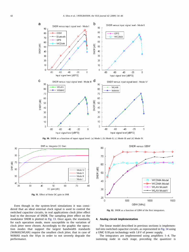
The simulated SNDR versus input signal level was simulatedand the above non-idealities included. The corresponding resultsdivided by the four operation modes are plotted in Fig. 10. Itcan be observed that the modes designed to operate with asingle standard (Modes II and IV) present better results whencompared with the other ones (Modes I and III) for the stan-
dards that can be processed in two different modes. On one hand,the single standard modes can be used to improve the perfor-mance of the conversion at the cost of hardware that lead tohigher power consumption. On the other hand, it is possible toreduce the power consumption if necessary and taking intoaccount the user’s requirements by switching the operation mode.
Nevertheless, the standards implemented with Modes I and IIIfor parallel processing are able to cope with the resolutionrequirements previously defined in Table 1.
The finite DC gain of the amplifier leads to a shift of theintegrators poles, changing the overall transfer functions. In thecascaded solutions, this problem is even more serious sincethe digital cancellation filters were calculated based on the idealtransfer functions and thus the error cancellation is not going tobe perfect.
To fully understand this issue, the degradation of the SNR wascalculated as a function of the finite gain, by recalculating thetransfer functions of all the operation modes with the non-idealtransfer function. The results obtained are plotted in Fig. 11. Basedon these results, a medium DC gain of 60 dB was chosen for theamplifiers.
The specifications of the amplifiers for the different standardsand operation modes are different. The gain bandwidth (GBW) ofthe modulator’s amplifiers is plotted in Fig. 12 for each modeof operation. The parameter of GBW considered correspondsto the first integrator, since this one presents the most strin-gent requirements of the entire modulator. For each operationmode the standards that required the larger values of GBW wereplotted.
ARTICLE IN PRESS
Fig. 10. SNDR as a function of input signal level: (a) Mode I, (b) Mode II, (c) Mode III and (d) Mode IV.
Fig. 11. Effect of finite DC gain in SNR
Fig. 12. SNDR as a function of GBW of the first integrators.
A. Silva et al. / INTEGRATION, the VLSI journal 42 (2009) 34–4642
Even though in the system-level simulations it was consi-dered that an ideal external clock signal is used to control theswitched capacitor circuits, in real applications clock jitter effectlead to the decrease of SNDR. The sampling jitter effect on themodulator SNDR is plotted in Fig. 13. Once again, the standards,for each operation mode, more susceptible to the variation ofclock jitter were chosen. Accordingly to the graphic the opera-tion modes that support the largest bandwidth standards(WiMAX/WLAN) require the smallest clock jitter, that in case ofWiMAX reach the 10 ps in order to not severely degrade theperformance.
4. Analog circuit implementation
The linear model described in previous sections is implemen-ted into switched capacitor circuits, as represented in Fig. 14 usinga UMC 0.18mm technology with 1.8 V of power supply.
The integrators are implemented using amplifiers 1–4. Thesumming node in each stage, preceding the quantizer is

ARTICLE IN PRESS
Fig. 13. SNDR as a function of sampling jitter.
A. Silva et al. / INTEGRATION, the VLSI journal 42 (2009) 34–46 43
implemented using amplifiers x–y, since a summing node basedon pure capacitive division would introduce a reduction factorthat would require compensation.
The telescopic cascode amplifier (Fig. 15) was chosen for theimplementation of the integrators and amplifiers, mainly due toits low power consumption and frequency response. When it isnot possible to obtain the desired gain, the gain-boostingtechnique is adopted, i.e. for the integrators of the widebandstandards of the sigma–delta modulator.
Performing the system-level simulations of the modulatorbased on MATLABs blocks, the specifications for the integrators ofall the operation modes were obtained. Taking into account thosevalues, for each operation mode, a different set of amplifierswould be required to face the requirements posed by thebehavioural simulations.
To avoid the implementation of such a large number ofdifferent amplifiers, the solution adopted consists in designingamplifier modules that are connected and operated in parallelaccording to the operation mode. Therefore, six amplifier’smodules were designed. Identical modules are connected inparallel when required.
Each amplifier block has two different sets of modules, i.e., twogroups of amplifiers, one is used for low-medium bandwidthstandards and the other for large bandwidth standards (WLANand WiMAX). The first group of amplifiers (Amp1, Amp2 andAmp5) is implemented recurring to telescopic amplifier. The otheramplifiers (Amp3, Amp4 and Amp6) are implemented using thesame structure previously discussed, telescopic with gain boost-ing enhancement.
The distribution of the amplifier’s modules is detailed inTable 7. For each amplifier block (part of the integrators orsumming nodes of the stages), the corresponding amplifiermodule (Amp1–6) and the number (]) of those modules operatedin parallel, for each operation mode, are described.
The specifications of the different modules are presented inTable 8 for single modules up to a maximum of four equalmodules connected in parallel.
Since the amplifiers used are implemented using a fullydifferential configuration, a common mode feedback (CMFB)circuit (Fig. 15) is required to sense the output voltage maintainingit ideally at the common mode voltage. To minimize the capacitiveloads, for each Ampx, only a switched capacitor CMFB circuit is
used. The drawback of this solution is the mismatch that couldlead to an offset in the common mode voltage, since only oneswitched capacitor CMFB circuit is used to control the amplifiermodules in parallel.
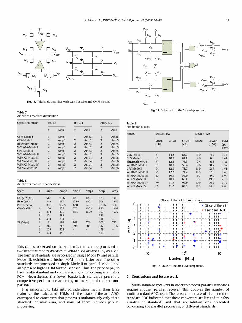
A 1.5 bit quantizer is implemented in the first two stages of thesigma–delta modulator. This tri-level quantizer also uses switchedcapacitor circuits as represented in Fig. 16. The reference voltagesof the ADC are subtracted in the switched capacitor part andtherefore built in threshold levels are not required in thecomparator.
During phase F2 the reference voltages are charged incapacitors CQ, while the comparator is in reset mode and thevalues from digital-to-analog conversion are being fed to the firstintegrator sampling capacitors. During the next phase, thecomparator performs the comparison of the input voltage minusthe reference voltage previously stored on capacitor CQ. Thesignals a, b and c control the DAC switches according to the resultsof the comparators.
The switches used in the sigma–delta modulator are imple-mented using CMOS switches and bootstrapped switches. Thelatter are used on the switches connected to the input signal andthe former are used in the remaining modulator switches.
Bootstrapped switches are used at the input to enhance theswitches linearity, i.e., keeping a constant resistance over theinput signal’s range voltage to avoid signal’s distortion to degradethe modulator performance. Nevertheless, these switches cansuffer from reliability issues due to the voltage applied to thetransistors gate that can become higher than the power supply,which can lead to device degradation.
The switches that drive the reference signals are designed forequal impedances improving the linearity of the switch. The otherswitches are designed so that the both transistors have the samesizes minimizing the resistance for the same dimensions, whencompared with the latter ones.
By using a fully differential implementation the problem ofcharge injection is eliminated since there is a common modecharge injection. However, at integrator’s sampling front-end,charge errors are signal dependent due to the charge injection as afunction of input signal, which originates signal dependentdistortion. To overcome this effect a two-phase non-overlappingclock with delayed versions has been used.
Therefore, opening switch F1 before F1d, does not cause signaldependent charge injection and this enables subsequent openingof F1d minimizing the previous effect, since the top plate of Cs isnow floating and a high impedance is seen by the transistorresulting in the flow of the majority charge to input.
To generate the phases that control the switches of themodulator, a traditional phase generator with non-overlappedclock phases and delayed versions is used. Due to the parallelprocessing mode, two standards can be processed simultaneouslyby using different stages. Thus, two-phase generators are requiredto provide different sampling frequencies to the modulator withthe different clock signals fed externally according to the selectedprocessing modes.
The performance of sigma–delta modulator is measured basedon spectral analysis, by determining the SNDR and consequenteffective number of bits. The obtained results are detailed inTable 9. Nevertheless, there are some considerations to take intoaccount. The simulation at device level of the modulator is anextremely time-consuming process. Therefore it was possibleneither to simulate all the operation modes at the desiredprecision nor to include all the designed analog blocks, namelythe phase generator and the respective buffers. To validate thecorrect behaviour of the phase generator included in the circuit,this analog block was used to generate the different frequencyphases for GSM Mode I and Bluetooth Mode I, not degrading the

ARTICLE IN PRESS
Φ1Φ1
Φ1Φ2
Φ1 Φ Φ1
Φ2Φ2 Φ1
Φ2
+-++
+-
-
-C s1 Cs2
Ci1 Ci2
Cn1
Cn3
Cn2
U1+
U2+
Φ1Φ1
Φ1
Φ2
Φ1 Φ2 Φ1
Φ2
Φ2 Φ1 Φ2
Ci1 Ci2
Cn3
Cn2
U1-
21
Φ2
Φ2
VDACp
VDACn
-+
+-x
U2-
Cf1
Φ1Φ1
Φ 1Φ 2
Φ1 Φ2 Φ1
Φ2Φ2 Φ1
Φ2
+-++
+-
-
-C s3 Cs4
Ci3 Ci4
Cn4
Cn6
Cn5
U2+
U3+
Φ1Φ1
Φ1
Φ2
Φ1 Φ2 Φ1
Φ2
Φ2 Φ1 Φ2
Ci3 Ci4
Cn7
Cn5
U2-
43
Φ2
Φ2
VDACp
VDACn
U3-
U3+
U3-
Time Alignment & Digital Correction
Stage 1
Stage 2
Stage 3
Stage 4
Stage5
1.5b 1.5b1.5b 1.5b 2b
Y1
Y3
Φ2
Φ2
Φ 2
Φ1
Φ2
Cf1 Φ2
Φ1
Φ2
-+
+-y
Cf2Φ2
Φ1
Φ2
Cf2 Φ2
Φ1
Φ2
Y2
Φ2
Φ2
2
Fig. 14. Schematic of modulator-switched capacitor circuit.
A. Silva et al. / INTEGRATION, the VLSI journal 42 (2009) 34–4644
overall performance of the modulator. For the wideband modes(WLAN and WiMAX) a latched comparator modelled in Verilog-AMS with 10 mV offset was introduced and the results shownbellows were obtained with this block.
The device level simulation results are detailed and comparedwith the behavioural results previously obtained in Fig. 10. Ingeneral, the presented results are similar to the ones predicted inprevious analysis. The margin difference to the behavioural resultsis acceptable, since the accuracy and the higher abstraction levelof behavioural simulations are not comparable with the device-level simulations. It was not possible to include thermal noise inthe transient simulations. Thus, to maintain the coherence of thesimulated results, the estimated thermal noise was included inthe total SNDR, with the obtained results considering the thermalnoise presented in Table 9, and the calculated figure of merit(FOM) values based on these values.
To clearly identify the potential of the proposed solution acomparison with the state-of-the-art multi-standard converters isperformed, recurring to the general FOM (13), where the powercorresponds to the power consumption, BW is the modulatorbandwidth and ENOB is the effective number of bits calculatedbased on the peak SNDR:
FOM ¼Power
2� BW� 2ENOB(13)
The FOMs of state-of-the-art multi-standard ADCs presented inTables 2 and 3 are calculated for each supported standard and areplotted in Fig. 17. All the standards supported by the presentedmodulator in each operation mode are also plotted in the samegraph. From the analysis of Fig. 17, it is possible to verify that themodes designed to process the signal concurrently present ahigher FOM when compared to their counterparts in single mode.
ARTICLE IN PRESS
M7
M5
M9
M3
M1
M2
M4
M6
M8
+ -+-
+ -+-
Vin+ Vin-
Vout- Vout+
Vctr
Vb3
Φ2
Φ2
Φ2
Φ1
Φ1
Φ1
Vcm
C1
C1
C2
C2
Vout+
Vout-Vcm
Vctr Vb
Fig. 15. Telescopic amplifier with gain boosting and CMFB circuit.
Table 7Amplifier’s modules distribution
Operation mode Int. 1,3 Int. 2,4 Amp. x, y
] Amp ] Amp ] Amp
GSM-Mode I 1 Amp1 1 Amp2 1 Amp5
GPS-Mode I 2 Amp1 2 Amp2 2 Amp5
Bluetooth-Mode I 2 Amp1 2 Amp2 2 Amp5
WCDMA-Mode I 4 Amp1 4 Amp2 4 Amp5
GPS-Mode II 2 Amp1 2 Amp2 2 Amp5
WCDMA-Mode II 3 Amp1 3 Amp2 3 Amp5
WiMAX-Mode III 2 Amp3 2 Amp4 2 Amp6
WLAN-Mode III 2 Amp3 2 Amp4 2 Amp6
WiMAX-Mode IV 2 Amp3 2 Amp4 2 Amp6
WLAN-Mode IV 2 Amp3 2 Amp4 2 Amp6
Table 8Amplifier’s modules specifications
Specs ] Amp1 Amp2 Amp3 Amp4 Amp5 Amp6
DC gain (dB) 61.2 63.6 101 100 62.1 101
Ibias (mA) 340 187 1340 1002 301 1340
Power (mW) 0.856 0.579 4.48 3.88 0.785 4.48
GBW (MHz) 1 156 238 670 1003 286 1065
2 288 430 1150 1630 506 1675
3 401 581 – – 676 –
4 499 704 – – 811 –
SR (V/ms) 1 121 139 443 574 206 762
2 214 217 697 885 347 1186
3 269 302 – – 459 –
4 328 340 – – 556 –
Fig. 16. Schematic of the 3-level quantizer.
Table 9Simulation results
Modes System level Device level
SNDR
(dB)
ENOB SNDR
(dB)
ENOB Power
(mW)
FOM
(pJ/
conv)
GSM Mode I 87 14.2 85.7 13.9 4.2 1.33
GPS Mode I 62 10.0 61.1 9.9 6.3 3.41
Bluetooth Mode I 77 12.5 76.3 12.4 6.3 1.18
WCDMA Mode I 62 10.0 59.4 9.6 10.7 3.52
GPS Mode II 74 12.0 73.7 11.9 12.7 1.61
WCDMA Mode II 75 12.2 71.2 11.5 17.0 1.43
WiMAX Mode III 62 10.0 59.9 9.7 49.0 3.04
WLAN Mode III 62 10.0 60.1 9.7 49.0 2.70
WiMAX Mode IV 70 11.3 65.9 10.6 74.6 2.32
WLAN Mode IV 69 11.2 63.9 10.3 74.6 2.63
Fig. 17. State-of-the-art FOM comparison.
A. Silva et al. / INTEGRATION, the VLSI journal 42 (2009) 34–46 45
This can be observed on the standards that can be processed intwo different modes, as cases of WiMAX/WLAN and GPS/WCDMA.The former standards are processed in single Mode IV and parallelMode III, exhibiting a higher FOM in the latter one. The otherstandards are processed in single Mode II or parallel Mode I andalso present higher FOM for the last case. Thus, the price to pay tohave multi-standard and concurrent signal processing is a higherFOM. Nevertheless, the lower bandwidth standards present acompetitive performance according to the state-of-the-art com-parison.
It is important to take into consideration that in their largemajority, the calculated FOMs of the state-of-the-art ADCscorrespond to converters that process simultaneously only threestandards at maximum, and none of them includes parallelprocessing.
5. Conclusions and future work
Multi-standard receivers in order to process parallel standardsrequire another parallel receiver. This doubles the number ofmulti-standard ADCs used. The research on state-of-the-art multi-standard ADC indicated that these converters are limited to a fewnumber of standards and that no solution was presentedconcerning the parallel processing of different standards.

ARTICLE IN PRESS
A. Silva et al. / INTEGRATION, the VLSI journal 42 (2009) 34–4646
Thus, a solution based on an extremely flexible architecturewith four distinguishable operation modes was presented. Theproposed architecture has a flexibility supported on the excellentmulti-standard characteristics of sigma–delta modulators, beingable to process six different standards with the option of parallelprocessing of two of them.
A system-level simulation including some of the expected non-idealities in the analog design was performed to confirm thefeasibility of the proposed solution with the obtained results,leading to implementation of the modulator at device level. Themodulator was implemented recurring to switched capacitorcircuits and simulated at device level.
The presented work aims at full integration of the proposedreconfigurable analog-to-digital converter, so that the resultsobtained from the system-level simulations can be confirmed bydevice-level simulation. The converter will then be submitted tointegration in UMC 0.18mm technology.
References
[1] B.G. Evans, K. Baughan, Visions of 4G, Electron. Commun. Eng. J. 12 (2000)293–303.
[2] J.G. Atallah, M. Ismail, Future 4G front-ends enabling smooth verticalhandoversaper, IEEE Circuits Devices Mag. 22 (2006) 6–15.
[3] S. Frattasi, H. Fathi, F.H.P. Fitzek, R. Prasad, M.D. Katz, Defining 4G technologyfrom the user’s perspective, IEEE Network 20 (2006) 35–41.
[4] S.Y. Hui, K.H. Yeung, Challenges in the migration to 4G mobile systems, IEEECommun. Mag. 41 (2003) 54–59.
[5] J. Craninckx, et al., A fully reconfigurable software-defined radio transceiver in0.13mm CMOS, in: Proceedings of the ISSCC, 2007, pp. 346–607.
[6] N. Ghittori, A. Vigna, P. Malcovati, S. D’Amico, A. Baschirotto, Analog basebandchannel for reconfigurable multistandard (GSM/UMTS/WLAN/Bluetooth)receivers, in: Proceedings of the WIRTEP, 2006, pp. 88–92.
[7] M. Brandolini, P. Rossi, D. Manstretta, F. Svelto, Toward multistandard mobileterminals—fully integrated receivers requirements and architectures, IEEETrans. Microwave. Theory Tech. 53 (2005) 1026–1038.
[8] A.A. Abidi, Direct-conversion radio transceivers for digital communication,IEEE J. Solid-State Circuits 30 (1995) 1399–1410.
[9] T. Burger, et al., A 13.5 mW 185-Msample/s DS modulator for UMTS/GSMdual-standard IF reception, IEEE J. Solid-State Circuits 36 (2001) 1868–1878.
[10] G. Gomez, et al., A 1.5 V 2.4/2.9 mW 79/50 dB DR SD modulator for GSM/WCDMA in 0.13mm digital process, in: Proceedings of the ISSCC, 2002,pp. 242–490.
[11] A. Dezzani, E. Andre, A 1.2 V dual-mode WCDMA/GPRS. SD modulator, in:Proceedings of the ISSCC, 2003, pp. 58–59.
[12] R.H.M. van Veldhoven, A tri-mode continuous-time SD modulator withswitched-capacitor feedback DAC for a GSM/EDGE/CDMA2000/UMTS recei-ver, in: Proceedings of the ISSCC, 2003, pp. 60–61.
[13] M.R. Miller, et al., A multibit sigma–delta ADC for multimode receivers, IEEE J.Solid-State Circuits 38 (2003) 475–482.
[14] B. Xia, A. Valdes-Garcia, E. Sanchez-Sinencio, A configurable time-interleavedpipeline ADC for multi-standard wireless receivers, in: Proceedings of theESSCIRC, 2004, pp. 259–262.
[15] J.H. Shim, et al., A third-order SD modulator in 0.18mm CMOS with calibratedmixed-mode integrators, IEEE J. Solid-State Circuits 40 (2005) 918–925.
[16] G. Gielen, E. Goris, Reconfigurable front-end architectures and A/D convertersfor flexible wireless transceivers for 4G radios, in: Proceedings of the ESAT-MICAS, 2004, pp. 13–18.
[17] J. Lim, et al., A low-power sigma–delta modulator for wireless communicationreceivers using adaptive biasing circuitry and cascaded comparator scheme,Analog Integrated Circuits Signal Process. (2006) 359–365.
[18] T. Christen, T. Burger, Q. Huang, A 0.13mm CMOS EDGE/UMTS/WLAN tri-modeDS ADC with -92 dB THD, in: Proceedings of the ISSCC, 2007, pp. 240–599.
[19] B. Putter, A Fifth-order CT/DT multi-mode DS modulator, in Proceedings.ISSCC, 2007, 244–245.
[20] S. Ouzounov, et al., A 1.2 V 121-mode CT DS modulator for wireless receiversin 90 nm CMOS, in: Proceedings of the ISSCC, 2007, pp. 242–600.
[21] A. Morgado, et al., An adaptive SD modulator for multi-standard hand-heldwireless devices, in: Proceedings of the ASSCC, 2007, pp. 232–235.
[22] A. Xotta, A. Gerosa, A. Neviani, A programmable-order sigma–delta converterfor a multi-standard wireless receiver, in: Proceedings of the WoWCAS, 2004,pp. 33–34.
[23] B.J. Farahani, M. Ismail, A low power multi-standard sigma delta ADC forWCDMA/GSM/Bluetooth applications, in: Proceedings of the NEWCAS, 2004,pp. 241–243.
[24] A. Rusu, B.R. Jose, M. Ismail, H. Tenhunen, A dual-band sigma–deltamodulator for GSM/WCDMA receivers, in: Proceedings of the DCIS, 2004,pp. 673–676.
[25] A. Rusu, A. Borodenkov, M. Ismail, H. Tenhunen, A triple-mode sigma–deltamodulator for multi-standard wireless radio receivers, J. Analog IntegratedCircuits Signal Process. 47 (2006) 113–124.
[26] A. Rusu, D.R.L. Gonzalez, M. Ismail, Reconfigurable ADCs enable smart radiosfor 4G wireless connectivity, IEEE Circuits Devices Mag. (2006).
[27] A. Gerosa, A. Xotta, A. Bevilacqua, A. Neviani, An A/D converter for multimodewireless receivers, based on the cascade of a doublesampling SD modulatorand a flash converter, IEEE Trans. Circuits Syst. I 53 (10) (2006).
[28] R. Schoofs, M.S.J. Steyaert, W.M.C. Sansen, A design-optimized continuous-time delta–sigma ADC for WLAN applications, IEEE Trans. Circuits Syst. I 54(2007) 209–217.
[29] G. Mitteregger, et al., A 20 mW 640 MHz CMOS continuous-time sigma–deltaADC with 20 MHz signal bandwidth, 80 dB dynamic range and 12-bit ENOB,IEEE J. Solid-State Circuits 41 (2006) 2641–2649.
[30] R. Schreier, G.C. Themes, Understanding Delta–Sigma Data Converters, Wiley,New York, 2005.
[31] P. Kiss, J. Silva, A. Wiesbauer, T. Sun, U. Moon, J. Stonick, G.C. Temes, Adaptivedigital correction of analog errors in MASH ADC’s—Part II: correction usingtest-signal injection, IEEE Trans. Circuits Syst. II 47 (2000) 629–638.
[32] R.T. Baird, T.S. Fiez, Linearity enhancement of multibit SD A/D and D/Aconverters using data weighted averaging, IEEE Trans. Circuits Syst. II 42(1995) 753–762.
[33] J. Silva, U. Moon, J. Steensgaard, G.C. Temes, A wideband low-distortiondelta–sigma ADC topology, Electron. Lett. 37 (2001) 737–738.
[34] T. Leslie, B. Singh, An improved sigma–delta modulator architecture, in:Proceedings of the ISCAS, 1990, pp. 372–375.
[35] M. Ortmanns, F. Gerfers, Y. Manoli, A continuous-time sigma–delta modulatorwith reduced jitter sensitivity, in: Proceedings of the ESSCIRC, 2002,pp. 287–290.
[36] J.A. Cherry, W.M. Snelgrove, Excess loop delay in continuous-time delta–sigma modulators, IEEE J. Solid-State Circuits (1999) 376–389.
[37] R. Schreier, J. Silva, J. Steensgaard, G.C. Temes, Design-oriented estimation ofthermal noise in switched-capacitor circuits, IEEE Trans. Circuits Syst. I 52(2005) 2358–2368.
[38] S. Brigati, F. Francesconi, P. Malcovati, D. Tonietto, A. Baschirotto, F. Maloberti,Modeling sigma–delta modulator non-idealities in simulink, in: Proceedingsof the ISCAS, 1999, pp. 384–387.
Artur Silva received the M.Sc. degree in Electrical andComputer Engineering from Instituto Superior Tecnico,Technical University of Lisbon, Portugal, in 2007.During 2006-2007 he worked as a researcher inIntegrated Circuits and Systems Group at Instituto deTelecomunicac- oes, Lisbon. Currently he works as aDesign Engineer with Integration Portugal. His currentresearch interests are focused on Sigma-Delta mod-ulators and switched capacitor circuits.
Jorge Guilherme received the M.Sc. and Ph.D. degreesfrom Instituto Superior Tecnico, Lisbon in 1994 and2003, in the area of microelectronics. He joined theElectrical and Computer Engineering Department atthe Instituto Politecnico Tomar in 1996. Since 2003, heis, also, a researcher at Instituto de Telecomunicac- oes.His research interests are in the areas of microelec-tronics, data conversion and power management. Hehas worked in the microelectronics area since 1990and has published more than 45 papers. He hasworked for 10 years in Arakit in the area of electronicsand was the head of the technical department. He
joined Chipidea in 1999 as an analogue designerworking in the field of data converters and powermanagement.Nuno Horta received the Licenciado, M.Sc. and Ph.D.degrees in electrical engineering from Instituto Super-ior Tecnico (IST), Technical University of Lisbon,Portugal, in 1989, 1992 and 1997, respectively. InMarch 1998, he joined the IST Electrical and ComputerEngineering Department. Since 1998, he is, also, aresearcher at Instituto de Telecomunicac- oes. Hisresearch interests are in the design of analog andmixed-signal integrated circuits, and especially inanalog and mixed-signal computer-aided design toolsand design automation. Dr. Horta has authored or co-authored more than 50 papers in international journals
and conferences. He has also participated as researcheror main researcher in several National and EuropeanR&D projects.