Recent Trends in Optical Lithography - Semantic …...• ROTHSCHILD ET AL. Recent Trends in Optical...
16
VOLUME 14, NUMBER 2, 2003 LINCOLN LABORATORY JOURNAL 221 O , of patterning, has enabled semiconductor de- vices to progressively shrink since the incep- tion of integrated circuits more than three decades ago. Throughout the 1980s and 1990s, the trend of miniaturization continued unabated and even accel- erated. Current semiconductor devices are being mass produced with 130-nm dense features; by 2007 these devices will have 65-nm dense features. Optical li- thography has been, and will remain for the foresee- able future, the critical technology that makes this trend possible. (To learn the fundamentals of optical lithography, see the sidebar entitled “Optical Lithog- raphy Primer.”) In 1993, a consortium of semiconductor manu- facturers called SEMATECH (for Semiconductor Manufacturing Technology) began periodically pub- Recent Trends in Optical Lithography Mordechai Rothschild, Theodore M. Bloomstein, Theodore H. Fedynyshyn, Roderick R. Kunz, Vladimir Liberman, Michael Switkes, Nikolay N. Efremow, Jr., Stephen T. Palmacci, Jan H.C. Sedlacek, Dennis E. Hardy, and Andrew Grenville ■ The fast-paced evolution of optical lithography has been a key enabler in the dramatic size reduction of semiconductor devices and circuits over the last three decades. Various methods have been devised to pattern at dimensions smaller than the wavelength used in the process. In addition, the patterning wavelength itself has been reduced and will continue to decrease in the future. As a result, it is expected that optical lithography will remain the technology of choice in lithography for at least another decade. Lincoln Laboratory has played a seminal role in the progress of optical lithography; it pioneered 193-nm lithography, which is used in advanced production, and 157-nm lithography, which is under active development. Lincoln Laboratory also initiated exploration of liquid- immersion lithography and studied the feasibility of 121-nm lithography. Many of the challenges related to practical implementation of short-wavelength optical lithography are materials-related, including engineering of new materials, improving on existing materials, and optimizing their photochemistry. This article examines the technical issues facing optical lithography and Lincoln Laboratory’s contributions toward their resolution. lishing the Technology Roadmap for Semiconductors, which assesses and predicts semiconductor technol- ogy requirements [1]. Technological and market forces have resulted in critical dimensions for semi- conductor chips that outpace the critical dimensions predicted by any editions of the Technology Roadmap. Lincoln Laboratory has played a seminal role in the progress of optical lithography. In 1988, when most of the lithography community was solving diffi- culties in the nascent 248-nm lithography, Lincoln Laboratory started a systematic development of 193- nm lithography with argon fluoride (ArF) excimer la- sers. A transition to the shorter wavelength required the solution of several material-science challenges, in- cluding improving on the transmission and durability of lens materials and coatings, and the development of transparent and etch-resistant photoresists. With
Transcript of Recent Trends in Optical Lithography - Semantic …...• ROTHSCHILD ET AL. Recent Trends in Optical...
• ROTHSCHILD ET AL.Recent Trends in Optical Lithography
VOLUME 14, NUMBER 2, 2003 LINCOLN LABORATORY JOURNAL 221
O , ofpatterning, has enabled semiconductor de-vices to progressively shrink since the incep-
tion of integrated circuits more than three decadesago. Throughout the 1980s and 1990s, the trend ofminiaturization continued unabated and even accel-erated. Current semiconductor devices are being massproduced with 130-nm dense features; by 2007 thesedevices will have 65-nm dense features. Optical li-thography has been, and will remain for the foresee-able future, the critical technology that makes thistrend possible. (To learn the fundamentals of opticallithography, see the sidebar entitled “Optical Lithog-raphy Primer.”)
In 1993, a consortium of semiconductor manu-facturers called SEMATECH (for SemiconductorManufacturing Technology) began periodically pub-
Recent Trends inOptical LithographyMordechai Rothschild, Theodore M. Bloomstein, Theodore H. Fedynyshyn,Roderick R. Kunz, Vladimir Liberman, Michael Switkes, Nikolay N. Efremow, Jr.,Stephen T. Palmacci, Jan H.C. Sedlacek, Dennis E. Hardy, and Andrew Grenville
■ The fast-paced evolution of optical lithography has been a key enabler in thedramatic size reduction of semiconductor devices and circuits over the last threedecades. Various methods have been devised to pattern at dimensions smallerthan the wavelength used in the process. In addition, the patterning wavelengthitself has been reduced and will continue to decrease in the future. As a result, itis expected that optical lithography will remain the technology of choice inlithography for at least another decade. Lincoln Laboratory has played a seminalrole in the progress of optical lithography; it pioneered 193-nm lithography,which is used in advanced production, and 157-nm lithography, which is underactive development. Lincoln Laboratory also initiated exploration of liquid-immersion lithography and studied the feasibility of 121-nm lithography. Manyof the challenges related to practical implementation of short-wavelength opticallithography are materials-related, including engineering of new materials,improving on existing materials, and optimizing their photochemistry. Thisarticle examines the technical issues facing optical lithography and LincolnLaboratory’s contributions toward their resolution.
lishing the Technology Roadmap for Semiconductors,which assesses and predicts semiconductor technol-ogy requirements [1]. Technological and marketforces have resulted in critical dimensions for semi-conductor chips that outpace the critical dimensionspredicted by any editions of the Technology Roadmap.
Lincoln Laboratory has played a seminal role inthe progress of optical lithography. In 1988, whenmost of the lithography community was solving diffi-culties in the nascent 248-nm lithography, LincolnLaboratory started a systematic development of 193-nm lithography with argon fluoride (ArF) excimer la-sers. A transition to the shorter wavelength requiredthe solution of several material-science challenges, in-cluding improving on the transmission and durabilityof lens materials and coatings, and the developmentof transparent and etch-resistant photoresists. With
• ROTHSCHILD ET AL.Recent Trends in Optical Lithography
222 THE LINCOLN LABORATORY JOURNAL VOLUME 14, NUMBER 2, 2003
is a com-plex process used to mass-pro-duce patterned silicon wafers insemiconductor manufacturing.Most integrated circuits are pat-terned with this technique.
Figure A illustrates a reductionprojection lithography systemcommonly used in optical lithog-raphy. A laser shines ultravioletlight first through an illuminator,which expands, homogenizes,and conditions the beam, andthen through a photomask,which contains the pattern to beimaged onto the wafer. The waferis coated with a photosensitivematerial, the photoresist. A com-plex projection lens reduces thephotomask pattern by a factor offour or five, and images it ontothe photoresist.
Advanced lithography systemsimage the photomask patternonto each wafer many times, in atwo-step process called step andscan. In the scanning part, por-tions of the photomask are im-aged onto the wafer in a continu-ous scanning motion, until thewhole photomask pattern istransferred to the wafer. In thenext stepping part, the wafer ismoved to a new location, and thescanning is repeated. Because thewafer production rate, orthroughput, significantly affectswafer costs, step-and-scan sys-tems are designed to pattern a
full wafer in less than a minute.The imaging (exposure) step is
followed by the developmentstep, where the exposed portionsof the photoresist are removed,leaving behind the desired pat-tern, which is then transferred tothe underlying wafer through anetch process. The sequence ofcoating the wafer with photore-sist, exposing it with ultravioletlight, developing it, and etchingit is repeated many times to com-plete the integrated circuit.
The performance of the pro-jection system is ultimately deter-mined by the laws governing the
O P T I C A L L I T H O G R A P H Y P R I M E R
propagation of electromagneticwaves. In lithography, there aretwo key metrics: the resolution,or the ability of the system to dis-tinguish between nearby features,and the depth of focus, which is ameasure of the precision withwhich the surface of the wafermust be positioned. Both quanti-ties depend on the patterningwavelength l and the numericalaperture (NA), the latter beingequal to nsinq, where q is thehalf-angle of the converging raysin the imaging system (see FigureA) and n is the index of refractionof the medium in contact withthe photoresist. The expressionsgoverning resolution and depthof focus are
resolution =NA
k1l (1)
and
depth of focus =(NA)2
k2l . (2)
The coefficients of propor-tionality k1 and k2 are measuresof the difficulty in printing agiven dimension with a given ex-posure system-photoresist com-bination. These values reflect sev-eral factors, including the effectof novel illumination modes andphotomasks, and improved pho-toresist performance. In more ad-vanced devices k1 is 0.4 and k2 is0.7. When patterning equal lines
FIGURE A. Reduction projectionlithography system.
Opticalintegrator
Illuminator
Laserlight
Condenserlens
Photomask
Projectionlens
Wafer
θ
• ROTHSCHILD ET AL.Recent Trends in Optical Lithography
223 THE LINCOLN LABORATORY JOURNAL VOLUME 14, NUMBER 2, 2003
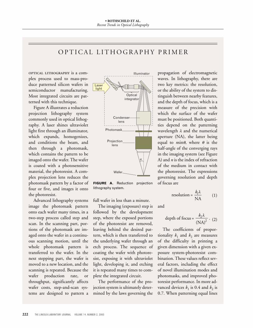
and spaces, the fundamentallower limit of k1 is 0.25, deter-mined by diffraction. For othergeometries, k1 can be smaller.
Equation 1 indicates that im-proved resolution can be ob-tained by reducing the wave-
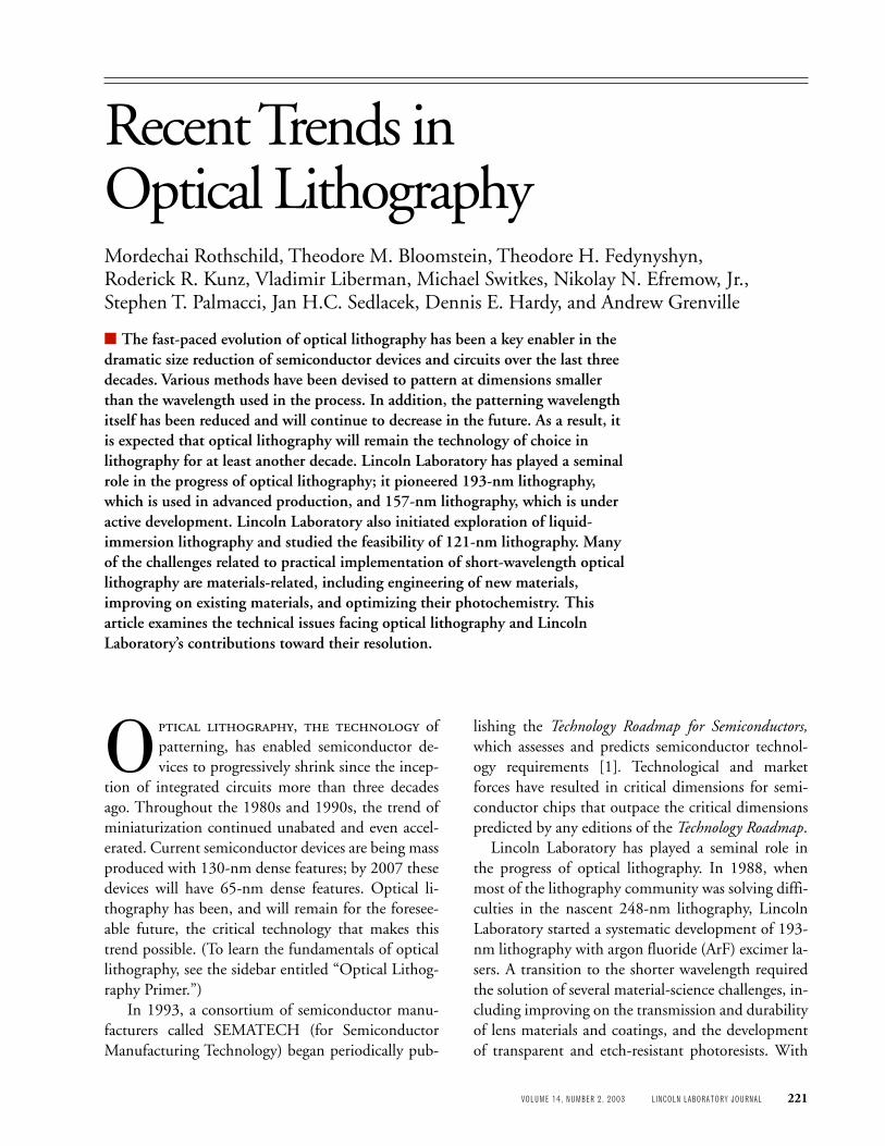
about 30% every two years. Onaverage, the number of transis-tors in an integrated circuit hasdoubled every eighteen months.This trend, shown in Figure B, isknown as Moore’s law because itwas recognized by GordonMoore in 1965.
Keeping pace with Moore’slaw has been the main challengeof optical lithography. To thisend, optical lithography hastaken on the complex techno-logical challenge of using deepultraviolet lasers and fabricatingoptics with very high NAs andnear-diffraction-limited perfor-mance, as discussed elsewhere inthis article. An equally impressiveeffort is taking place in develop-ing strategies to reduce k1, with-out changing the wavelength orimaging optics. When the mini-mum feature size became lessthan the wavelength, k1 becameless than the NA and optical li-thography entered the era ofsubwavelength imaging. Thistransition, which took placearound 1996, is shown in FigureC as the intersection between theexposure-wavelength curve (or-ange) and the minimum-feature-size curve (green). The reductionin k1 was facilitated by severalfactors, described in the compan-ion article in this issue by Fritzeet al., entitled “SubwavelengthOptical Lithography with Phase-Shift Photomasks.” These factorsinclude modified illuminationschemes and changes in the pat-tern on the photomask.
length l of the laser and by in-creasing the NA of the imagingsystem. Continued improve-ments in optical lithography haveenabled the printing of ever finerfeatures, with the smallest size, orcritical dimension, decreasing by
FIGURE B. Logarithmic plot showing how the number of transistors placed ona microprocessor chip increases according to Moore’s law.
FIGURE C. Reduction in minimum feature size and exposure wavelength overtime. Mercury arc lamps produce the G-line at 436 nm and the I-line at 365 nm.The krypton-fluoride (KrF) excimer laser operates at 248 nm, the argon-fluoride(ArF) laser operates at 193 nm, and the fluorine (F2) excimer laser operates at157 nm.
' 70 ' 72 ' 74 ' 76 ' 78 ' 80 ' 82 ' 84 ' 88 ' 90 ' 92 ' 94 ' 96 ' 98 ' 00 ' 02
107
108
106
105
104
103
Year of introduction
4004
Z80008085
8086
68000 80286
68040 80486
Super sparc Pentium
ItaniumPentium IV
AlphaAthlon
8080
Num
ber o
f tra
nsis
tors
/chi
p
20003000
436G-line
15001000
600
365I-line
400KrF248 ArF
193F2157
90
130150180
250350
Exposure wavelengthMinimum feature size
' 88 ' 90 ' 92 ' 94 ' 96 ' 98 ' 00 ' 02 ' 04' 80 ' 82 ' 84 ' 860.05
0.10
1.0
10.0
Above wavelength SubwavelengthNearwavelength
Year
Feat
ure
size
(nm
)

• ROTHSCHILD ET AL.Recent Trends in Optical Lithography
224 LINCOLN LABORATORY JOURNAL VOLUME 14, NUMBER 2, 2003
support from the Defense Advanced ResearchProjects Agency (DARPA), Lincoln Laboratory facili-tated much of the development in these areas, largelythrough collaborations with suppliers and researchlaboratories [2]. It also had built and installed in itsclean rooms the world’s first 193-nm large-field pro-jection lithography system [3], and fabricated the firstdevices at 193 nm [4].
By 1996, when it became apparent that 193-nm li-thography would indeed become the next technology,we started studying the feasibility of 157-nm lithog-raphy, the wavelength of fluorine (F2) excimer lasers[5]. (Although the actual wavelength used is 157.6nm, the lithography community shortens this valueto 157 nm.) Lithography at 193 nm was introducedinto advanced manufacturing in 2001; 157-nm li-thography is expected to follow in its path around2005. In 2000, on the heels of these programs, webegan exploring two new directions in optical lithog-raphy: increasing the numerical aperture (NA) be-yond 1.0 by using immersion liquids [6], and short-ening the wavelength further to 121 nm [7]. Thisarticle summarizes the current status of these tech-nologies in which Lincoln Laboratory continues toplay an important role—157-nm lithography, liquid-immersion lithography, and 121-nm lithography.
Lithography at 157 nm
The transition from 193- to 157-nm lithography re-quires several important changes in the projectionsystems, the photomasks, and the photoresists. Forthe projection systems there are three new issues toconsider. First, the lens material must be exclusivelycrystalline calcium fluoride, whereas at 193 nm manyelements are fabricated of fused silica. Second, the op-tical coatings require new materials, mostly fluoridethin films. And third, the ambient must be high-pu-rity nitrogen, with well-controlled levels of potentialcontaminants.
In general, issues encountered at 193 nm are moredifficult to resolve at 157 nm because of the shorterwavelength. The change to optics made of calciumfluoride at 157 nm requires the growth of crystals ofmuch higher quality than needed at 193 nm. The ab-sorption coefficient must be less than 0.002 cm–1 atthe new wavelength, which imposes stringent require-
ments on the impurity levels in the starting materialsand in the final crystal. (Note that throughout thisarticle, absorption coefficients are given in base 10,not base e.) The inhomogeneities in refractive indexmust be less than 1 part per million (ppm), and theresidual stress-induced birefringence must be lessthan 1 nm/cm, both values implying near-perfectcrystal growth.
Because of these requirements, the crystal-growingcompanies have made large investments in technol-ogy development and infrastructure. The optical li-thography market has generated an explosive expan-sion in the fluoride-crystal-growth industry, driving amanifold increase in capacity and quality in just a fewyears. Still, the industry’s current yield of near-perfectcrystals is low at present. Unless there are significantimprovements in the crystal-growth process, the de-mand for calcium fluoride crystals may not be metfrom 2005 to 2008, the ramp-up years of 157-nmlithography.
An added complication to the calcium-fluoridesituation was the realization in early 2001 that cal-cium fluoride has an intrinsic birefringence that can-not be reduced by the crystal growth or annealingprocess [8]. This intrinsic birefringence is caused bythe interaction between the laser electric field and thecrystal lattice, and therefore it is both deterministicand dependent on the angle of propagation and crys-talline orientation. Also, it is much larger at 157 nmthan at 193 nm. To overcome this problem, it is nec-essary to employ lenses made of calcium fluoride withtwo different crystalline orientations. Again, crystalgrowers bear the burden of ensuring that high-yieldprocesses are available to grow high-quality crystals,this time in both orientations.
Practically every optical element requires a thin-film coating for antireflective purposes. The mostcommon coatings are antireflective. These consist ofseveral layers of dielectric thin films, each having athickness of approximately one quarter wavelengthand alternating in their refractive index between highand low. Of course, these dielectric films must behighly transparent, and at 157 nm this requirementimplies the use of metal fluorides. High-index materi-als are lanthanum fluoride or gadolinium fluoride;low-index materials are magnesium fluoride or alumi-
• ROTHSCHILD ET AL.Recent Trends in Optical Lithography
VOLUME 14, NUMBER 2, 2003 LINCOLN LABORATORY JOURNAL 225
num fluoride. Oxide films used at longer wave-lengths, such as silicon dioxide or hafnium oxide, areusually too absorptive at 157 nm. The near-universaluse of fluoride thin films introduces a level of uncer-tainty because they must be qualified with respect totheir antireflective properties as well as their durabil-ity upon long-term exposure to laser radiation.
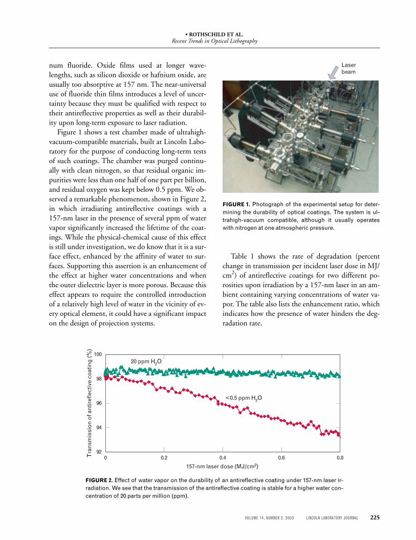
Figure 1 shows a test chamber made of ultrahigh-vacuum-compatible materials, built at Lincoln Labo-ratory for the purpose of conducting long-term testsof such coatings. The chamber was purged continu-ally with clean nitrogen, so that residual organic im-purities were less than one half of one part per billion,and residual oxygen was kept below 0.5 ppm. We ob-served a remarkable phenomenon, shown in Figure 2,in which irradiating antireflective coatings with a157-nm laser in the presence of several ppm of watervapor significantly increased the lifetime of the coat-ings. While the physical-chemical cause of this effectis still under investigation, we do know that it is a sur-face effect, enhanced by the affinity of water to sur-faces. Supporting this assertion is an enhancement ofthe effect at higher water concentrations and whenthe outer dielectric layer is more porous. Because thiseffect appears to require the controlled introductionof a relatively high level of water in the vicinity of ev-ery optical element, it could have a significant impacton the design of projection systems.
Table 1 shows the rate of degradation (percentchange in transmission per incident laser dose in MJ/cm2) of antireflective coatings for two different po-rosities upon irradiation by a 157-nm laser in an am-bient containing varying concentrations of water va-por. The table also lists the enhancement ratio, whichindicates how the presence of water hinders the deg-radation rate.
FIGURE 1. Photograph of the experimental setup for deter-mining the durability of optical coatings. The system is ul-trahigh-vacuum compatible, although it usually operateswith nitrogen at one atmospheric pressure.
Laser beam
FIGURE 2. Effect of water vapor on the durability of an antireflective coating under 157-nm laser ir-radiation. We see that the transmission of the antireflective coating is stable for a higher water con-centration of 20 parts per million (ppm).
92
94
96
98
100
0 0.2 0.4 0.6 0.8Tra
nsm
issi
on o
f ant
iref
lect
ive
coat
ing
(%)
157-nm laser dose (MJ/cm2)
20 ppm H2O
<0.5 ppm H2O
• ROTHSCHILD ET AL.Recent Trends in Optical Lithography
226 LINCOLN LABORATORY JOURNAL VOLUME 14, NUMBER 2, 2003
The cleanliness of the purge gas is also of para-mount importance at 157 nm. Photoinduced con-tamination of optics due to trace contaminants in thepurge gas has already been observed at 248 and 193nm, and the shorter wavelength of 157 nm only exac-erbates this effect. Furthermore, scattered 157-nm ra-diation is more effective at decomposing organic ma-terials, thereby liberating volatile contaminants,which in turn may form photoinduced deposits onoptical surfaces. Over the past four years we have useda sensitive gas-chromatograph mass spectrometer totest over one hundred materials for such photoin-duced outgassing. Tested materials include opticaladhesives, tubing for purge gases, and photoresists[9]. The concern over detrimental effects of photo-outgassing is not unique to lithography. In fact, thephenomenon is akin to similar effects in space opticsprograms, where our gas-chromatograph mass-spec-trometer system has been useful in identifying photo-induced contamination reactions.
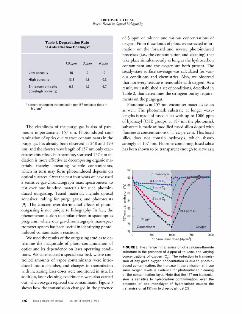
We used the results of the outgassing studies to de-termine the magnitude of photo-contamination ofoptics and its dependence on laser operating condi-tions. We constructed a special test bed, where con-trolled amounts of vapor contaminants were intro-duced into a chamber, and changes in transmissionwith increasing laser doses were monitored in situ. Inaddition, laser-cleaning experiments were also carriedout, when oxygen replaced the contaminant. Figure 3shows how the transmission changed in the presence
of 3 ppm of toluene and various concentrations ofoxygen. From these kinds of plots, we extracted infor-mation on the forward and reverse photoinducedprocesses (i.e., the contamination and cleaning) thattake place simultaneously as long as the hydrocarboncontaminant and the oxygen are both present. Thesteady-state surface coverage was calculated for vari-ous conditions and chemistries. Also, we observedthat not every residue is removable with oxygen. As aresult, we established a set of conditions, described inTable 2, that determines the stringent purity require-ments on the purge gas.
Photomasks at 157 nm encounter materials issuesas well. The photomask substrate at longer wave-lengths is made of fused silica with up to 1000 ppmof hydroxyl (OH) groups; at 157 nm the photomasksubstrate is made of modified fused silica doped withfluorine at concentrations of a few percent. This fusedsilica does not contain hydroxyls, which absorbstrongly at 157 nm. Fluorine-containing fused silicahas been shown to be transparent enough to serve as a
Table 1. Degradation Rateof Antireflective Coatings*
1.5 ppm 3 ppm 6 ppm
Low porosity 10 2 2
High porosity 13.3 1.6 0.3
Enhancement ratio 0.8 1.3 6.7(low/high porosity)
*percent change in transmission per 157-nm laser dose inMJ/cm2
FIGURE 3. The change in transmission of a calcium-fluoridesubstrate in the presence of 3 ppm of toluene, and varyingconcentrations of oxygen (O2). The reduction in transmis-sion at any given oxygen concentration is due to photoin-duced contamination; the increase in transmission at thesesame oxygen levels is evidence for photoinduced cleaningof the contamination layer. Note that the 157-nm transmis-sion is sensitive to hydrocarbon contamination; even thepresence of one monolayer of hydrocarbon causes thetransmission at 157 nm to drop by almost 2%.
76
78
80
82
84
86
88
90
92
0 500 1000 1500 2000157-nm laser dose (J/cm2)
<0.4 ppm O2
1.2 ppm O2
1.9 ppm O2
3.4 ppm O2
Oxygen
Oxygen +
Contaminant
157
-nm
tran
smis
sion
(%)
~1 monolayer

• ROTHSCHILD ET AL.Recent Trends in Optical Lithography
VOLUME 14, NUMBER 2, 2003 LINCOLN LABORATORY JOURNAL 227
photomask substrate, and it is also resistant to laser-induced damage [10].
The absorber in binary photomasks is the tradi-tional chromium-based stack of thin films. Severalabsorptive materials have been proposed for attenuat-ing phase-shift photomasks, and it appears that prac-tical options may become available [11]. The largestuncertainty with the photomask at 157 nm is not re-lated to the photomask itself, but to the means re-quired to protect it from particle contamination.There is essentially zero tolerance to particles landingon the photomask, because of the severe yield impli-cations of even one particle in the wrong place.Therefore, the accepted method of protecting thephotomask has been to use a very thin membrane, thepellicle, which is placed several millimeters away from
the photomask. Because of the standoff, particles onthe pellicle are out of focus, and a high process yieldcan be maintained. The pellicles at 193 and 248 nmare submicrometer-thick fluoropolymers, chosen fortheir mechanical properties as well as for their trans-mission and their laser durability [12].
At 157 nm, the situation is much more complex.Several pellicle candidates meet the mechanical andtransmission requirements, but to date all materialshave exhibited rapid degradation in 157-nm trans-mission when irradiated with a 157-nm laser. A com-mon benchmark used to asses the durability of pel-licle materials is the 10% lifetime, which is the laserdose that changes the transmission of the pellicle by10%. For practical use in industry, this value must beat least 100 J/cm2, and probably 1 kJ/cm2. Figure 4
Table 2. Effects of 157-nm Photoinduced Contamination of Optical SurfacesCaused by Contaminants in the Ambient
Low Levels High Levels
Hydrocarbons Reversible Irreversible
Parts-per-billion levels limit surface losses Brief exposure (< 1 kJ/cm2) to ppmto < 0.1% in sub-ppm levels of oxygen. levels can lead to permanent degradation.
Organosilicons Irreversible Irreversible
Parts-per-trillion levels are necessary tolimit growth of SiO2 over lifetime of tool.
Fluorocarbons No contamination No contamination at > 10 ppm
FIGURE 4. 10% lifetime of pellicle material samples tested. The 10% lifetime is defined as the incident laserdose that produces a 10% change in the transmission of the pellicle material with a thickness of 0.8 mm.
0
1
2
3
4
5
6
7
Samples
10%
life
time
(J/c
m2 )

• ROTHSCHILD ET AL.Recent Trends in Optical Lithography
228 LINCOLN LABORATORY JOURNAL VOLUME 14, NUMBER 2, 2003
shows that the 10% lifetime of all pellicle materialstested at 157 nm is less than 7 J/cm2, which is at leastone and probably two orders of magnitude less thanwhat is needed, given the number of wafers that areexposed for each photomask. The failure mode of thepellicles is loss of transmission, a process named pho-tochemical darkening. The underlying photochemis-try is complex, but it is probably initiated by photo-generated free radicals, which then form a range ofunsaturated bonds.
While active research is ongoing to reduce photo-chemical darkening, an alternative approach has beenengineered that uses thin inorganic plates as hard pel-licles. The hard pellicles are made of the fluorinatedfused-silica material used in photomask blanks. Be-cause of manufacturing limitations, they are about800 mm thick, not as thin as soft pellicles. They mustbe viewed as an additional optical element in the pro-jection system, which means that they must meetstringent requirements of flatness and uniformity,and even their mounting is critical. Nevertheless, atpresent hard pellicles are more promising than softpellicles, because of the uncertainty of controllingphotochemical darkening.
Photoresists at 157 nm have encountered a differ-ent set of challenges. The thickness of photoresists isdetermined by two opposing considerations. In orderto maintain a good photoresist profile after develop-ment, it has been customary to set an upper limit onthe absorption of photoresists. An optical density of0.4 is an accepted value for this upper limit, and thisvalue translates into a lower limit of transmission ofabout 40%. The optical density is the product of ab-sorption coefficient and thickness; therefore, themore transparent the photoresist, the thicker it canbe. Traditional hydrocarbon polymers have 157-nmabsorption coefficients of approximately 6 mm–1, im-plying that the maximum photoresist thickness is lessthan 70 nm. While the absorption coefficient deter-mines the upper limit of the photoresist thickness,processing considerations set a lower limit of approxi-mately 200 nm (for the 65-nm node). Thus the ab-sorption coefficient of 157-nm photoresists must bereduced to approximately 2 mm–1, or maybe even less.
The last several years have witnessed a continuousreduction in the absorption coefficient of 157-nm
photoresists, accomplished primarily by the incorpo-ration of C-F bonds and the elimination of C-H, un-saturated, and aromatic bonds along with carbonylgroups in the polymer. Of course, the new materialsmust retain all the excellent photo-imaging propertiesof the more established photoresists, as well as theirplasma-etch resistance. Fortunately, the basic chemi-cal amplification scheme that works so effectively at248 and 193 nm can still be used at 157 nm [13]. Thespecific chemistry and formulation of the photoresistentails various trade-offs. Still, resolution of 50 nmhas been shown with photoresists having a thicknessof 120 nm [14]. Absorption coefficients of even lessthan 1 mm–1 have been reported recently [15]. An-other promising approach to the development of157-nm photoresists is the incorporation of transpar-ent inorganic nanoparticles in the polymer [16]. Thisapproach accomplishes two goals simultaneously—increased transparency and enhanced plasma-etch re-sistance (lower etch rate), thus enabling a smallerthickness. Figure 5 shows plasma-etch rates of a com-mercially available photoresist modified with varyingamounts of silicon dioxide nanoparticles.
0
50
100
150
200
Basephotoresist
10% SiO2
20% SiO2
33% SiO2
50% SiO2
100% SiO2
Pla
sma-
etch
rat
e (n
m/m
in)
Oxygen plasmaChlorine plasma
Photoresist
FIGURE 5. Plasma-etch rates of photoresists incorporatingvarying amounts of inorganic nanoparticles, in differentreactive ion-etching chemistries (chlorine and oxygen). Thebase photoresist contains no silicon dioxide (SiO2). Reduc-tions of an order of magnitude in the plasma-etch rate canbe achieved with about 30% to 50% content of nanoparticles.
• ROTHSCHILD ET AL.Recent Trends in Optical Lithography
VOLUME 14, NUMBER 2, 2003 LINCOLN LABORATORY JOURNAL 229
In the aggregate, the various subsystems requiredfor a successful implementation of 157-nm lithogra-phy are in place. Lincoln Laboratory has performedpioneering research in many of these areas and con-tinues to be a significant technology contributor.
Liquid-Immersion Lithography
Liquid-immersion lithography achieves higher pat-terning resolutions not by reducing the patterningwavelength l in Equation 1 in the sidebar, but by in-creasing the NA beyond 1.0 through the use of im-mersion liquids. Equation 1 shows that, in additionto reducing l and k1, increasing the refractive index ofthe imaging medium results in higher resolution. Ifinstead of air or nitrogen, we employ a liquid with arefractive index n of about 1.4, then the maximumNA approaches 1.4, and a resolution enhancementproportional to n is achieved without changing wave-length, lasers, photomasks, and other establishedcomponents of the technology base.
The physics underlying this resolution enhance-ment is as follows: adding a liquid between the lastoptical element and the photoresist enables the cou-pling of rays that propagate at steep angles and thatwould otherwise be reflected through total internalreflection at the optics-air interface. This phenom-enon is the basis of oil-immersion microscopy, whichhas been used for over a century, and the newly engi-neered liquid-immersion lithography.
The differences between oil-immersion micros-copy and liquid-immersion lithography are more
practical than fundamental. One difference is thewavelength. To be useful, liquid-immersion lithogra-phy must be implemented at the deep ultraviolet(UV) wavelengths of 193 and 157 nm. At such shortwavelengths there are few transparent liquids. Fur-thermore, even small residual absorption can lead todetrimental photochemical reactions, which coulddegrade the liquid, the optical element in contactwith the liquid, or the photoresist in contact with theliquid. Another difference is that the field of viewmust be much larger in lithography than in micros-copy. The design of diffraction-limited imaging op-tics is therefore more complex in lithography. Thethird difference relates to the optical-mechanicalspecifications of the liquid. To be useful in lithogra-phy, any spatial or temporal variations of the indexshould be kept to a minimum, and no bubbles shouldbe present during imaging. Finally, since lithographicprojection systems are used in a step-and-scan mode,the engineering of handling the liquid in a high-speedscanning environment is critical.
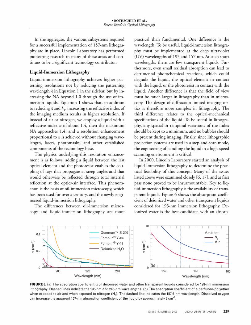
In 2000, Lincoln Laboratory started an analysis ofliquid-immersion lithography to determine the prac-tical feasibility of this concept. Many of the issueslisted above were examined closely [6, 17], and at firstpass none proved to be insurmountable. Key to liq-uid-immersion lithography is the availability of trans-parent liquids. Figure 6 shows the absorption coeffi-cient of deionized water and other transparent liquidsconsidered for 193-nm immersion lithography. De-ionized water is the best candidate, with an absorp-
FIGURE 6. (a) The absorption coefficient a of deionized water and other transparent liquids considered for 193-nm immersionlithography. Dashed lines indicate the 193-nm and 248-nm wavelengths. (b) The absorption coefficient of a perfluoro-polyetherwhen exposed to air and when exposed to nitrogen (N2). The dashed line indicates the 157.6-nm wavelength. Dissolved oxygencan increase the apparent 157-nm absorption coefficient of the liquid by approximately 3 cm–1.
Wavelength (nm)
0.4
0.2
0240220200
Demnum™ S-200
Fomblin® Y-04
Fomblin® Y-18
Deionized H2O(cm
–1)
α
10
5
0
Wavelength (nm)165160155
Ambient N2 Air
(cm
–1)
α
(b)(a)

• ROTHSCHILD ET AL.Recent Trends in Optical Lithography
230 LINCOLN LABORATORY JOURNAL VOLUME 14, NUMBER 2, 2003
tion coefficient of 0.036 cm–1, which enables a suffi-cient working distance of several millimeters for theoptical and mechanical designers of projection sys-tems. Note that for practical reasons, the working dis-tance must be at least approximately 1 mm. At 157nm, the most transparent liquids found to date havean absorption coefficient of approximately 3 cm–1, re-quiring a working distance of less than 0.1 mm. Toachieve a larger working distance, we must reduce theabsorption coefficient proportionally.
The transparent liquids under consideration be-long to the class of perfluoro-polyethers (PFPEs).These liquids, which are currently used as lubricantsand heat-transfer fluids, and their optical properties,such as transmission at 157 nm, have not been thesubject of optimization. For instance, hydrocarbonimpurities at the level of 10 ppm may be sufficient toaccount for most of the observed absorption at 157nm. Lincoln Laboratory has an active program toidentify the causes of the 157-nm absorption in theseliquids, and ultimately engineer a liquid transparentenough for immersion lithography. Indeed, we haverecently demonstrated the highest transparency ofany liquid at 157 nm, with an absorption coefficientof 0.5 cm–1. This value is within striking distance ofthe target needed in practical implementation.
Preliminary experiments at Lincoln Laboratoryhave focused on the possible photoinduced changesat the liquid-optics interface and at the liquid-photo-resist interface. A 157-nm antireflective optical coat-ing exposed to flowing PFPE under laser irradiationhas shown no degradation in transmission, up to atleast a 15-kJ/cm2 dose. Similarly, fused silica exposedto deionized water and 193-nm laser irradiation hasnot shown changes in transmission. Furthermore,angle-resolved forward scattering at 157 nm has notrevealed the existence of bubbles due to flowingPFPE, up to flow rates of at least 30 cm/min.
Interactions between the immersion liquid and thephotoresist may lead to subtle changes in photoresistperformance. Again, our initial experiments involv-ing contrast curves of 157-nm photoresists with andwithout PFPE during exposure indicate that no ma-jor changes take place. Figure 7 shows contrast curvesof three 157-nm photoresists exposed in semitrans-parent liquid, compared to their respective curves
when exposed in nitrogen; there is indication that inone photoresist a liquid-induced inhibition layer isformed, but this result must still be confirmed. Thin-ning of 193-nm photoresists by the liquid in the ab-sence of laser irradiation has been measured to be lessthan 0.5 nm, well within acceptable limits.
While many of these initial experiments are beingrefined and expanded, they nevertheless have shownthat no major roadblocks are expected in implement-ing liquid-immersion lithography. Largely as a resultof this work performed at Lincoln Laboratory, liquid-immersion lithography has emerged during the lastyear as a serious candidate for extending optical li-thography. In 2002 and 2003 SEMATECH orga-
FIGURE 7. Contrast curves of three 157-nm photoresists ex-posed in semitransparent liquid (immersion), compared totheir respective curves when exposed in nitrogen. The upperand middle photoresists show no change, while the bottomphotoresist exhibits behavior that can be attributed to theformation of a surface-inhibition layer.
1.0
0.5
0
1.0
0.5
0
1.20.80.4 0.6 1.00.20
1.20.80.4 0.6 1.00.20
1.20.80.4 0.6 1.00.20
1.0
0.5
0
Nor
mal
ized
thic
knes
s (T
0)
Immersion
Nitrogen
Normalized dose (E0)

• ROTHSCHILD ET AL.Recent Trends in Optical Lithography
VOLUME 14, NUMBER 2, 2003 LINCOLN LABORATORY JOURNAL 231
nized formal workshops on this topic; one of theiroutcomes was an accelerated set of feasibility studies,several of which are being carried out at LincolnLaboratory. If these studies are successful, liquid-im-mersion lithography at 193 nm would be used toprint 45-nm devices, and at 157 nm it would be em-ployed in patterning 32-nm features. These dimen-sions are projected to be mass produced in the year2007 or later.
Lithography at 121 nm
The shortest UV wavelength to be used in optical li-thography may possibly be 121.6 nm, the wavelengthof the Lyman-a line of atomic hydrogen. If feasible,lithography at 121 nm would enable extension ofprojection dry lithography in a direct path extendingfrom 248 to 193 to 157 nm, and then to 121 nm. Aswith any new lithographic wavelength, many issuesmust be examined and then overcome before this pat-terning wavelength can be introduced into manufac-turing. Lincoln Laboratory has explored the varioussubsystems at 121 nm [7]. Some appear to requirerelatively minor engineering changes, but others maybe more difficult to solve.
One advantage of 121-nm lithography over alter-natives such as extreme ultraviolet (EUV) at 13-nmor electron-beam lithography is that vacuum-basedsystems are not necessary. In fact, the absorption coef-ficient at 121 nm of most common purge gases andatmospheric constituents is similar to, and even lowerthan, that at 157 nm. Therefore, lithographic systemscan be engineered by using best practices similar tothose used at 157 nm.
The main deviation from 157-nm lithographywould be the use of pulsed discharge sources at 121nm instead of lasers. Because convenient lasers havenot been demonstrated at 121 nm, we would resort tohydrogen-containing plasmas. This approach is notnovel. Mercury plasmas have been used in lithogra-phy at 436 and 365 nm, and even in the early phasesof 248 nm. They are also being engineered for futureEUV lithography. Indeed, in an initial experiment weemployed a focused plasma system optimized forEUV and showed that approximately 6%, or about0.5 J/pulse, of the stored capacitor energy can be gen-erated at 121 nm. This efficiency was one order of
magnitude higher than that at EUV, holding theprospect of powerful 121-nm plasma sources for li-thography even in the absence of lasers.
The biggest challenge to date in 121-nm lithogra-phy is the lack of suitably transparent optical materi-als. Projection systems at 121 nm would have to usehigh NAs over 0.75, which almost certainly demandsoptical designs that require lenses, either all refractive(using only lenses) or catadioptric (a combination oflenses and mirrors). Therefore, highly transparentlens materials are essential. Because of the short wave-length, it appears that only a few crystalline fluorideshave the requisite high band gap. The primary candi-date is lithium fluoride (LiF), which is often used aswindow material for detecting Lyman-a radiation.However, the absorption coefficient required in li-thography applications would be about five timeslower than that of the most transparent LiF that wehave identified, i.e., approximately 0.02 cm–1 com-pared to the lowest measured 0.09 cm–1. The cause ofthe relatively high absorption coefficient has not yetbeen determined, but it is probably related to thepresence of lithium oxide or hydroxide in the crystal.Therefore, it should be possible to grow truly low-ab-sorption LiF under the appropriate ambient and an-nealing conditions. Such a demonstration must stillbe performed.
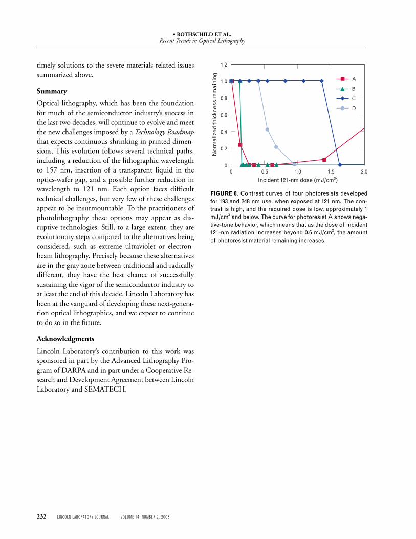
The next critical issue of any new lithographicwavelength is that of a suitable photoresist. Our stud-ies indicate that the basic photochemistry of polymersand additives is not qualitatively different at 121 nmthan at 157 or 193 nm. Therefore, the widely ac-cepted scheme of chemical amplification via pho-tolytically generated acids applies at 121 nm, and therequired incident doses presented in Figure 8 arequite low, about 1 mJ/cm2. The main difficulty in en-gineering photoresists at 121 nm is the universallyhigh absorption coefficient of organic polymers. Thisimplies the use of very thin layers of photoresist, ap-proximately 25 to 35 nm thick. These thicknesses areat least three times lower than those of the thinnestphotoresists used at 157 or 193 nm, and they may notbe compatible with pattern transfer processing stepssuch as reactive ion etching.
Photolithography at 121 nm is still a possibility,but to a large extent its success will be determined by
• ROTHSCHILD ET AL.Recent Trends in Optical Lithography
232 LINCOLN LABORATORY JOURNAL VOLUME 14, NUMBER 2, 2003
timely solutions to the severe materials-related issuessummarized above.
Summary
Optical lithography, which has been the foundationfor much of the semiconductor industry’s success inthe last two decades, will continue to evolve and meetthe new challenges imposed by a Technology Roadmapthat expects continuous shrinking in printed dimen-sions. This evolution follows several technical paths,including a reduction of the lithographic wavelengthto 157 nm, insertion of a transparent liquid in theoptics-wafer gap, and a possible further reduction inwavelength to 121 nm. Each option faces difficulttechnical challenges, but very few of these challengesappear to be insurmountable. To the practitioners ofphotolithography these options may appear as dis-ruptive technologies. Still, to a large extent, they areevolutionary steps compared to the alternatives beingconsidered, such as extreme ultraviolet or electron-beam lithography. Precisely because these alternativesare in the gray zone between traditional and radicallydifferent, they have the best chance of successfullysustaining the vigor of the semiconductor industry toat least the end of this decade. Lincoln Laboratory hasbeen at the vanguard of developing these next-genera-tion optical lithographies, and we expect to continueto do so in the future.
Acknowledgments
Lincoln Laboratory’s contribution to this work wassponsored in part by the Advanced Lithography Pro-gram of DARPA and in part under a Cooperative Re-search and Development Agreement between LincolnLaboratory and SEMATECH.
FIGURE 8. Contrast curves of four photoresists developedfor 193 and 248 nm use, when exposed at 121 nm. The con-trast is high, and the required dose is low, approximately 1mJ/cm2 and below. The curve for photoresist A shows nega-tive-tone behavior, which means that as the dose of incident121-nm radiation increases beyond 0.6 mJ/cm2, the amountof photoresist material remaining increases.
Incident 121-nm dose (mJ/cm2)
Nor
mal
ized
thic
knes
s re
mai
ning
1.2
1.0
0.8
0.6
0.4
0.2
0
A
B
C
D
0 0.5 1.0 1.5 2.0
• ROTHSCHILD ET AL.Recent Trends in Optical Lithography
VOLUME 14, NUMBER 2, 2003 LINCOLN LABORATORY JOURNAL 233
R E F E R E N C E S1. <http://www.sematech.org/public/corporate/history/
history.htm>2. M. Rothschild, R.B. Goodman, M.A. Hartney, M.W. Horn,
R.R. Kunz, J.H.C. Sedlacek, and D.C. Shaver, “Photolithog-raphy at 193 nm,” J. Vac. Sci. Technol. B 10 (6), 1992, pp.2989–2996.
3. M. Hibbs, R. Kunz, and M. Rothschild, “193-nm Lithographyat MIT Lincoln Lab,” Solid State Technol. 38 (7), 1995, pp. 69–78.
4. M. Rothschild, J.A. Burns, S.G. Cann, A.R. Forte, C.L. Keast,R.R. Kunz, S.C. Palmateer, J.H.C. Sedlacek, R. Uttaro, A.Grenville, and D. Corliss, “How Practical Is 193 nm Lithog-raphy?” J. Vac. Sci. Technol. B 14 (6), 1996, pp. 4157–4161.
5. T.M. Bloomstein, M.W. Horn, M. Rothschild, R.R. Kunz,S.T. Palmacci, and R.B. Goodman, “Lithography with 157 nmLasers,” J. Vac. Sci. Technol. B 15 (6), 1997, pp. 2112–2116.
6. M. Switkes and M. Rothschild, “Immersion Lithography at157 nm,” J. Vac. Sci. Technol. B 19 (6), 2001, pp. 2353–2356.
7. V. Liberman, M. Rothschild, P.G. Murphy, and S.T. Palmacci,“Prospects for Photolithography at 121 nm,” J. Vac. Sci.Technol. B 20 (6), 2002, pp. 2567–2573.
8. J.H. Burnett, Z.H. Levine, and E.L. Shirley, “Intrinsic Bire-fringence in Calcium Fluoride and Barium Fluoride,” Phys.Rev. B 64 (24), 2001, pp. 241102-1–241102-4.
9. R.R. Kunz, V. Liberman, and D.K. Downs, “Photo-InducedOrganic Contamination of Lithographic Optics,”Microlithogr. World 9 (1), 2000, pp. 2–9.
10. V. Liberman, T.M. Bloomstein, M. Rothschild, J.H.C.Sedlacek, R.S. Uttaro, A.K. Bates, C. Van Peski, and K. Orvek,“Materials Issues for Optical Components and Photomasks in157 nm Lithography,” J. Vac. Sci. Technol. B 17 (6), 1999, pp.3272–3279.
11. V. Liberman, M. Rothschild, S.J. Spector, K.E. Krohn, S.C.Cann, and S. Hien, “Attenuating Phase Shifting Mask at 157nm,” SPIE 4691, pt. 1, 2002, pp. 561–567.
12. V. Liberman, R.R. Kunz, M. Rothschild, J.H.C. Sedlacek, R.S.Uttaro, A. Grenville, A.K. Bates, and C. Van Peski, “DamageTesting of Pellicles for 193-nm Lithography,” SPIE 3334,1998, pp. 480–495.
13. R.R. Kunz, T.M. Bloomstein, D.E. Hardy, R.B. Goodman,D.K. Downs, and J.E. Curtin, “Outlook for 157 nm ResistDesign,” J. Vac. Sci. Technol. B 17 (6), 1999, pp. 3267–3272.
14. T. Itani, T. Suganaga, N. Kanda, J.-H. Kim, K. Watanabe,J. Cashmore, and M. Gower, “Effect of High Numerical Ap-erture Lens on Lithographic Performance in 157 nm Lithog-raphy,” J. Vac. Sci. Technol. B 20 (6), 2002, pp. 2562–2566.
15. S.-I. Kodama, I. Kaneko, Y. Takebe, S. Okada, Y. Kawaguchi,N. Shida, S. Ishikawa, M. Toriumi, and T. Itani, “Synthesis ofNovel Fluoropolymer for 157nm Photoresist by Cyclo-Poly-merization,” SPIE 4690, pt. 1, 2002, pp. 76–83.
16. T.H. Fedynyshyn, R.F. Sinta, M. Sworin, R.B. Goodman, S.P.Doran, I. Sondi, and E. Matijevic, “Encapsulated InorganicResist Technology Applied to 157-nm Lithography,” SPIE4345, pt. 1, 2001, pp. 308–318.
17. M. Switkes and M. Rothschild, “Resolution Enhancement of157 nm Lithography by Liquid Immersion,” SPIE 4691, pt. 1,2002, pp. 459–465.

• ROTHSCHILD ET AL.Recent Trends in Optical Lithography
234 LINCOLN LABORATORY JOURNAL VOLUME 14, NUMBER 2, 2003
. is a staff member in theSubmicrometer Technologygroup. Upon joining the staffat Lincoln Laboratory, heperformed the initial feasibilitystudy of optical lithography at157 nm, assessing opticalmaterials, potential photoresistcandidates, laser performance,and photomask related issues.He has constructed the world’sfirst 157-nm microstepper,which demonstrated 80-nmpatterning. Recently, he hasbeen investigating the effectsof surface contaminants on theperformance of optical materi-als and coatings at 157 nm.He earned a Sc.D. degree inelectrical engineering fromMIT. His doctoral thesis wason laser direct forming ofthree-dimensional structures insilicon.
leads the SubmicrometerTechnology group, where hisresponsibilities include manag-ing the advanced lithographyprojects at Lincoln Laboratory,as well as several other micro-fabrication activities. Prior tojoining Lincoln Laboratory in1984, he conducted research atthe University of Illinois andthe University of SouthernCalifornia in the areas of laserphotochemistry and laser-induced nonlinear processes,He received his Ph.D. degreein optics from the Universityof Rochester in 1979.
. .is a senior staff member of theSubmicrometer Technologygroup. He is an expert inphotoresist development andqualification, having served intechnical and program man-agement leadership roles atOlin, Shipley, and LincolnLaboratory for over twentyyears. He earned a Ph.Ddegree in chemistry fromBrown University in 1979.
. joined the SubmicrometerTechnology group in 1988 andhas been a senior staff memberthere since 1997. His principalfocus has been on the develop-ment of 193-nm photoresistprocesses, investigation ofexcimer-laser direct processes,and chemical sensing. Prior tojoining Lincoln Laboratory, hestudied the fundamentalaspects of particle-beam-induced deposition and etch-ing processes. He received aB.S. degree in chemistry fromRensselaer Polytechnic Insti-tute in 1983 and a Ph.D.degree in analytical chemistryfrom the University of NorthCarolina at Chapel Hill in1988. While earning hisdoctoral degree, Roderickworked at the IBM T.J.Watson Research Center,where he studied reactions ofatomic hydrogen on crystallinesilicon surfaces.
• ROTHSCHILD ET AL.Recent Trends in Optical Lithography
VOLUME 14, NUMBER 2, 2003 LINCOLN LABORATORY JOURNAL 235
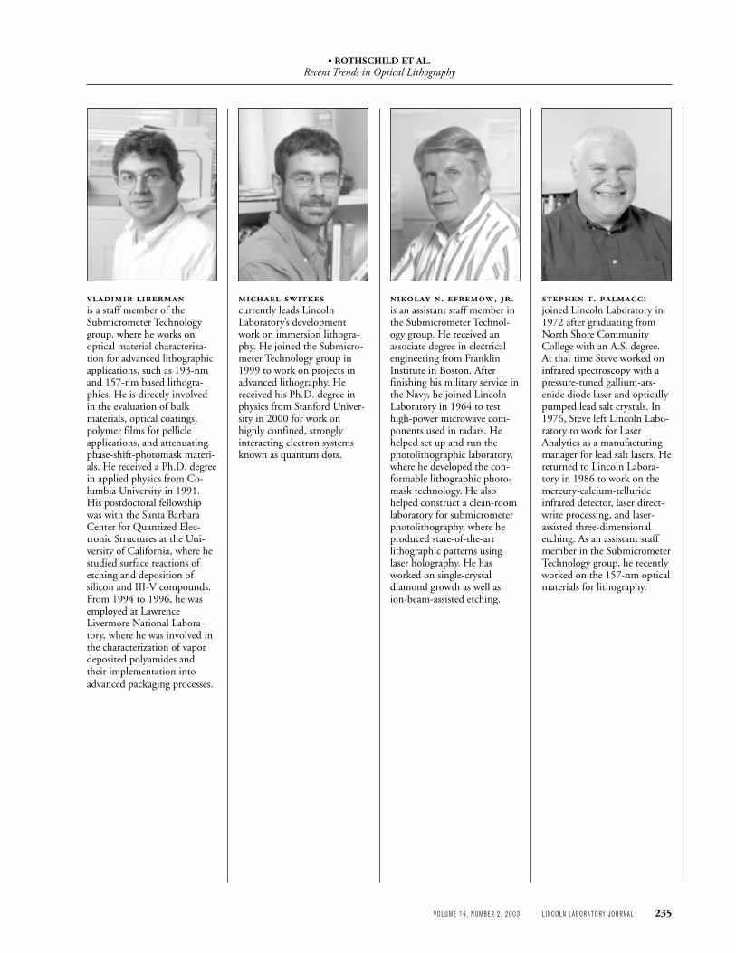
currently leads LincolnLaboratory’s developmentwork on immersion lithogra-phy. He joined the Submicro-meter Technology group in1999 to work on projects inadvanced lithography. Hereceived his Ph.D. degree inphysics from Stanford Univer-sity in 2000 for work onhighly confined, stronglyinteracting electron systemsknown as quantum dots.
is a staff member of theSubmicrometer Technologygroup, where he works onoptical material characteriza-tion for advanced lithographicapplications, such as 193-nmand 157-nm based lithogra-phies. He is directly involvedin the evaluation of bulkmaterials, optical coatings,polymer films for pellicleapplications, and attenuatingphase-shift-photomask materi-als. He received a Ph.D. degreein applied physics from Co-lumbia University in 1991.His postdoctoral fellowshipwas with the Santa BarbaraCenter for Quantized Elec-tronic Structures at the Uni-versity of California, where hestudied surface reactions ofetching and deposition ofsilicon and III-V compounds.From 1994 to 1996, he wasemployed at LawrenceLivermore National Labora-tory, where he was involved inthe characterization of vapordeposited polyamides andtheir implementation intoadvanced packaging processes.
. , .is an assistant staff member inthe Submicrometer Technol-ogy group. He received anassociate degree in electricalengineering from FranklinInstitute in Boston. Afterfinishing his military service inthe Navy, he joined LincolnLaboratory in 1964 to testhigh-power microwave com-ponents used in radars. Hehelped set up and run thephotolithographic laboratory,where he developed the con-formable lithographic photo-mask technology. He alsohelped construct a clean-roomlaboratory for submicrometerphotolithography, where heproduced state-of-the-artlithographic patterns usinglaser holography. He hasworked on single-crystaldiamond growth as well asion-beam-assisted etching.
. joined Lincoln Laboratory in1972 after graduating fromNorth Shore CommunityCollege with an A.S. degree.At that time Steve worked oninfrared spectroscopy with apressure-tuned gallium-ars-enide diode laser and opticallypumped lead salt crystals. In1976, Steve left Lincoln Labo-ratory to work for LaserAnalytics as a manufacturingmanager for lead salt lasers. Hereturned to Lincoln Labora-tory in 1986 to work on themercury-calcium-tellurideinfrared detector, laser direct-write processing, and laser-assisted three-dimensionaletching. As an assistant staffmember in the SubmicrometerTechnology group, he recentlyworked on the 157-nm opticalmaterials for lithography.
• ROTHSCHILD ET AL.Recent Trends in Optical Lithography
236 LINCOLN LABORATORY JOURNAL VOLUME 14, NUMBER 2, 2003
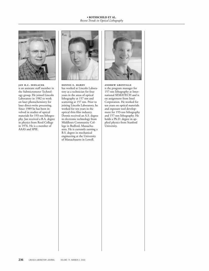
. has worked at Lincoln Labora-tory as a technician for fouryears in the areas of opticallithography at 157 nm andscattering at 157 nm. Prior tojoining Lincoln Laboratory, heworked for ten years in theoptical thin-film industry.Dennis received an A.S. degreein electronic technology fromMiddlesex Community Col-lege in Bedford, Massachu-setts. He is currently earning aB.S. degree in mechanicalengineering at the Universityof Massachusetts in Lowell.
.. is an assistant staff member inthe Submicrometer Technol-ogy group. He joined LincolnLaboratory in 1982 to workon laser photochemistry forlaser direct-write processing.Since 1989 he has been in-volved in studies of opticalmaterials for 193-nm lithogra-phy. Jan received a B.A. degreein physics from Reed Collegein 1976. He is a member ofAAAS and SPIE.
is the program manager for157-nm lithography at Inter-national SEMATECH and ison assignment from IntelCorporation. He worked forten years on optical materialsand exposure tool develop-ment for 193-nm lithographyand 157-nm lithography. Heholds a Ph.D. degree in ap-plied physics from StanfordUniversity.


![Milestones in Optical Lithography Tool Suppliers [Compatibility Mode]](https://static.fdocuments.in/doc/165x107/5868eafe1a28ab4a408c31c6/milestones-in-optical-lithography-tool-suppliers-compatibility-mode.jpg)