Recent progress in flexible and wearable bio …quanyuan.whu.edu.cn/pdf/2017NR.pdfRecent progress in...
24
Recent progress in flexible and wearable bio-electronics based on nanomaterials Yanbing Yang, Xiangdong Yang, Yaning Tan, and Quan Yuan ( ) Key Laboratory of Analytical Chemistry for Biology and Medicine (Ministry of Education), College of Chemistry and Molecular Sciences, Wuhan University, Wuhan 430072, China Received: 29 September 2016 Revised: 2 January 2017 Accepted: 5 January 2017 © Tsinghua University Press and Springer-Verlag Berlin Heidelberg 2017 KEYWORDS flexible biosensor, electronics, nanostructured materials, integrated devices, graphene ABSTRACT Flexible and stretchable biosensors that can monitor and quantify the electrical or chemical signals generated by specific microenvironments have attracted a great deal of attention. Wearable biosensors that can be intimately attached to skin or tissue provide a new opportunity for medical diagnostics and therapy. In recent years, there has been enormous progress in device integration and the design of materials and manufacturing processes for flexible and stretchable systems. Here, we describe the most recent developments in nanomaterials employed in flexible and stretchable biosensors. We review successful examples of such biosensors used for the detection of vital physiological and biological markers such as gas released from organisms. Furthermore, we provide a detailed overview of recent achievements regarding integrated platforms that include multifunctional nanomaterials. The issues and challenges related to the effective integration of multifunctional nanomaterials in bio-electronics are also discussed. 1 Introduction Flexible electronics may be incorporated into wearable devices that can accommodate dramatic mechanical deformations while maintaining stable performance [1‒4]. Recently, flexible biosensors have attracted the attention of researchers owing to their potential usefulness in personal healthcare and disease diagnosis [5‒8]. Flexible and wearable biosensors have several intriguing advantages; they are light-weight, ultra- conformable, portable, noninvasive, and implantable. They can be attached to the tissue surface and can con- tinuously and closely monitor physiological biomarkers and the electronic, electrochemical, thermal, mechanical, and biochemical signals emanating from the human body without interrupting or influencing an individual’s activities [9‒11]. Therefore, the development of inexpensive, wearable systems for the rapid in situ detection and measurement of vital signals in the human body provides an opportunity for designing point-of-care clinical devices for disease diagnosis, therapy, and health monitoring. Typically, flexible biosensors are composed of several essential parts: 1) a flexible substrate that supports the Nano Research 2017, 10(5): 1560–1583 DOI 10.1007/s12274-017-1476-8 Address correspondence to [email protected]
Transcript of Recent progress in flexible and wearable bio …quanyuan.whu.edu.cn/pdf/2017NR.pdfRecent progress in...

Recent progress in flexible and wearable bio-electronicsbased on nanomaterials
Yanbing Yang, Xiangdong Yang, Yaning Tan, and Quan Yuan ()
Key Laboratory of Analytical Chemistry for Biology and Medicine (Ministry of Education), College of Chemistry and Molecular Sciences, Wuhan University, Wuhan 430072, China
Received: 29 September 2016
Revised: 2 January 2017
Accepted: 5 January 2017
© Tsinghua University Press
and Springer-Verlag Berlin
Heidelberg 2017
KEYWORDS
flexible biosensor,
electronics,
nanostructured materials,
integrated devices,
graphene
ABSTRACT
Flexible and stretchable biosensors that can monitor and quantify the electrical
or chemical signals generated by specific microenvironments have attracted a
great deal of attention. Wearable biosensors that can be intimately attached to
skin or tissue provide a new opportunity for medical diagnostics and therapy.
In recent years, there has been enormous progress in device integration and the
design of materials and manufacturing processes for flexible and stretchable
systems. Here, we describe the most recent developments in nanomaterials
employed in flexible and stretchable biosensors. We review successful examples
of such biosensors used for the detection of vital physiological and biological
markers such as gas released from organisms. Furthermore, we provide a
detailed overview of recent achievements regarding integrated platforms that
include multifunctional nanomaterials. The issues and challenges related to the
effective integration of multifunctional nanomaterials in bio-electronics are also
discussed.
1 Introduction
Flexible electronics may be incorporated into wearable
devices that can accommodate dramatic mechanical
deformations while maintaining stable performance
[1‒4]. Recently, flexible biosensors have attracted the
attention of researchers owing to their potential
usefulness in personal healthcare and disease diagnosis
[5‒8]. Flexible and wearable biosensors have several
intriguing advantages; they are light-weight, ultra-
conformable, portable, noninvasive, and implantable.
They can be attached to the tissue surface and can con-
tinuously and closely monitor physiological biomarkers
and the electronic, electrochemical, thermal, mechanical,
and biochemical signals emanating from the human
body without interrupting or influencing an individual’s
activities [9‒11]. Therefore, the development of
inexpensive, wearable systems for the rapid in situ
detection and measurement of vital signals in the
human body provides an opportunity for designing
point-of-care clinical devices for disease diagnosis,
therapy, and health monitoring.
Typically, flexible biosensors are composed of several
essential parts: 1) a flexible substrate that supports the
Nano Research 2017, 10(5): 1560–1583
DOI 10.1007/s12274-017-1476-8
Address correspondence to [email protected]

www.theNanoResearch.com∣www.Springer.com/journal/12274 | Nano Research
1561 Nano Res. 2017, 10(5): 1560–1583
entire circuit and simultaneously conforms to irregular
structures [12‒14]; 2) electrodes or active materials
for electronic or optical signal export [15‒17]; and
3) specific sensing elements for recognizing analytes
[18‒21]. The development of flexible and stretchable
biosensors requires a novel approach to material design
regarding the selection of suitable nanomaterials and
the synthesis of new multifunctional nanomaterials
[22‒24]. New sensing materials, fabrication techniques,
and sensing mechanisms have significantly promoted
the development of flexible and stretchable biosensors
[25‒27]. Recently, research interest has focused on
multiple sensors that are integrated into a single sensor
network [28]. Such sensor systems are required to
simultaneously measure multiple stimuli because the
human body can generate physical information as well
as chemical and biological signals under stimulation.
Therefore, integrated systems with physical and
chemical or biological sensors are of vital importance
for the development of advanced flexible biosensors
with multiple functions [29]. The integration of
biosensors with medical treatment and data processing
systems is another requirement of wearable sensors
[30, 31]. More recently, a few research groups have
demonstrated integrated systems that combine pH
and glucose sensors with drug delivery systems for
diabetes diagnosis and therapy [32].
Here, we summarize the recent progress made in
the development of flexible and stretchable biosensors
that can be used as wearable devices, with regard
to the various nanomaterials, nanostructures, and
engineering technologies used. We provide a brief
introduction to the general working principle of
biosensors based on different types of components
used to monitor vital signals such as those pertaining
to heart and respiration rate, diabetes, DNA, and cancer
biomarkers. We also summarize detailed descriptions
of the development of flexible biosensors in con-
junction with device design. In particular, we provide
an overview of flexible biosensors with integrated
systems together with examples of flexible biosensors
reported in the literature. The issues and challenges
faced by flexible biosensors are comprehensively
discussed. Overall, in this review, we present the
recent advances in nanomaterials used in flexible
biosensors. We also provide an overview of the recent
progress made in the development of flexible bio-
electronics based on integrated device designs. The
challenges and future opportunities presented by
flexible biosensors based on nanomaterials are also
discussed.
2 Materials for flexible biosensors
The flexible substrate plays an important role in
device development because it acts as a mechanical
support for active materials and electronic circuits.
Apart from flexibility, the substrate should be bendable,
stretchable, transparent, and even biodegradable.
Polyethylene terephthalate (PET) and polyimide (PI)
are the most widely used substrates in flexible biosensor
fabrication owing to their high thermal and chemical
resistance [33‒36]. In addition to flexibility, the
remarkable elasticity of polydimethylsiloxane (PDMS)
makes it the best choice for stretchable sensors [37, 38].
Natural biomaterials such as silk are considered
excellent candidates for implantable biosensors owing
to their excellent characteristics such as biocompati-
bility, biodegradability, and natural abundance [39,
40]. Large area patterned conducting polymers such
as polypyrrole (PPy), polyaniline (PANI), and poly-
thiophene can also be used as the active materials
in biosensors [41‒43]. The polythiophene derivative
poly(3,4-ethylenedioxythiophene):poly(styrene sulfonate)
(PEDOT:PSS) is the most commonly used organic
semiconductor for chemical and biological sensing
applications [44].
Recently, nanomaterials have been explored in
the context of flexible biosensor applications because
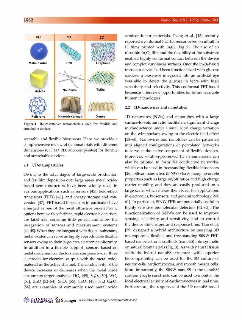
they provide tunable nanostructures. Figure 1 shows
representative nanomaterials used in flexible and
stretchable devices. Nanomaterials can be patterned
to form films or arrays to provide mechanical flexibility,
thereby resolving the intrinsic mechanical mismatch
between rigid devices and curvilinear biological
structures. Furthermore, the nanoscale dimensions
of nanostructured materials endow them with large
surface areas that significantly increase the effective
contact area, which is an advantage for flexible
biosensors that require high sensitivity. The develop-
ment of nanomaterials with favorable electrical and
mechanical properties facilitates the fabrication of
| www.editorialmanager.com/nare/default.asp
1562 Nano Res. 2017, 10(5): 1560–1583
Figure 1 Representative nanomaterials used for flexible and stretchable devices.
wearable and flexible biosensors. Here, we provide a
comprehensive review of nanomaterials with different
dimensions (0D, 1D, 2D, and composites) for flexible
and stretchable devices.
2.1 0D-nanoparticles
Owing to the advantages of large-scale production
and fast film deposition over large areas, metal oxide-
based semiconductors have been widely used in
various applications such as sensors [45], field-effect
transistors (FETs) [46], and energy storage and con-
version [47]. FET-based biosensors in particular have
emerged as one of the most attractive bio-electronic
options because they facilitate rapid electronic detection,
are label-free, consume little power, and allow the
integration of sensors and measurement systems
[44, 48]. When they are integrated with flexible substrates,
metal oxides can serve as highly reproducible flexible
sensors owing to their large-area electronic uniformity.
In addition to a flexible support, sensors based on
metal oxide semiconductors also comprise two or three
electrodes for electrical output, with the metal oxide
material as the active channel. The conductivity of the
device increases or decreases when the metal oxide
encounters target analytes. TiO2 [49], V2O5 [50], WO3
[51], ZnO [52‒54], SnO2 [55], In2O3 [45], and Ga2O3
[56] are examples of commonly used metal oxide
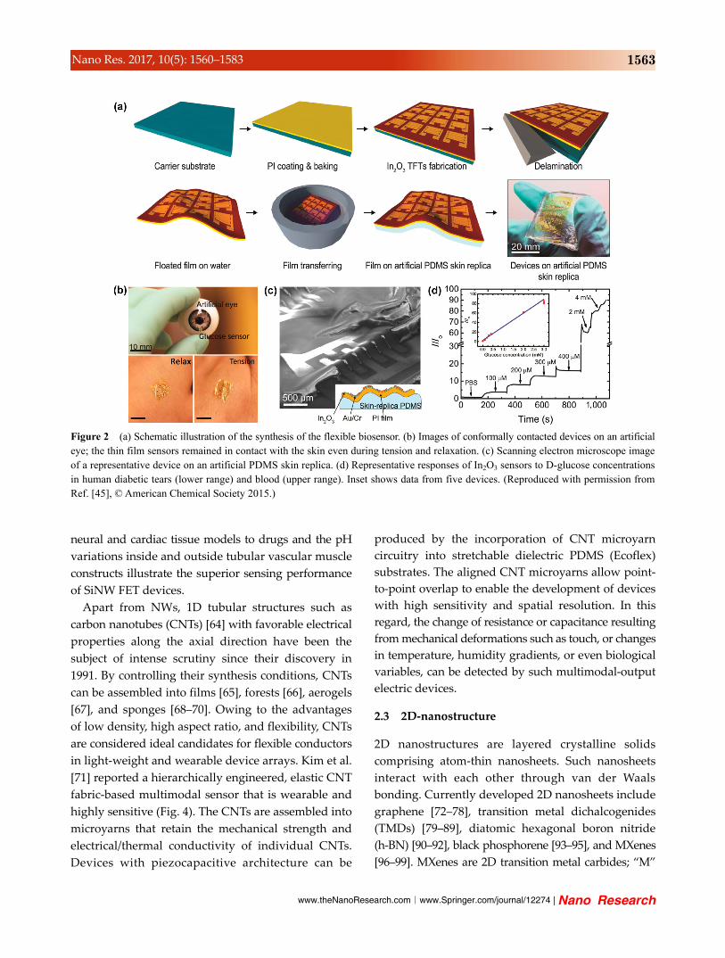
semiconductor materials. Tseng et al. [45] recently
reported a conformal FET biosensor based on ultrathin
PI films printed with In2O3 (Fig. 2). The use of an
ultrathin In2O3 film and the flexibility of the substrate
enabled highly conformal contact between the device
and complex curvilinear surfaces. Once the In2O3-based
transistor device had been functionalized with glucose
oxidase, a biosensor integrated into an artificial eye
was able to detect the glucose in tears with high
sensitivity and selectivity. This conformal FET-based
biosensor offers new opportunities for future wearable
human technologies.
2.2 1D-nanowires and nanotubes
1D nanowires (NWs) and nanotubes with a large
surface-to-volume ratio facilitate a significant change
in conductance under a small local charge variation
on the wire surface, owing to the electric field effect
[58‒60]. Nanowires and nanotubes can be patterned
into aligned configurations or percolated networks
to serve as the active component of flexible devices.
Moreover, solution-processed 1D nanomaterials can
also be printed to form 3D conductive networks,
which can be used in freestanding flexible biosensors
[26]. Silicon nanowires (SiNWs) have many favorable
properties such as large on/off ratios and high charge
carrier mobility, and they are easily produced on a
large scale, which makes them ideal for applications
in electronics, biosensors, and general technology [60,
61]. In particular, SiNW FETs are potentially useful in
highly sensitive biomolecular detectors [62, 63]. The
functionalization of SiNWs can be used to improve
sensing selectivity and sensitivity, and to control
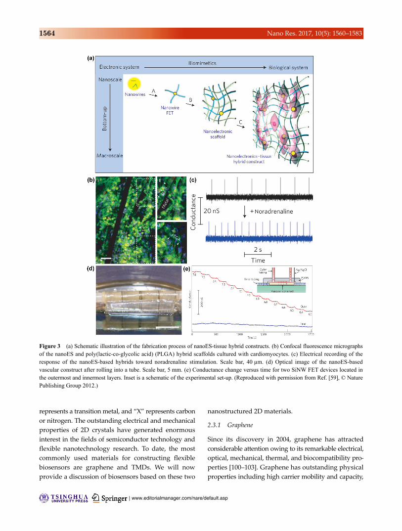
the device dimensions and response time. Tian et al.
[59] designed a hybrid architecture by inserting 3D
macroporous, flexible, and free-standing SiNW FET-
based nanoelectronic scaffolds (nanoES) into synthetic
or natural biomaterials (Fig. 3). As with natural tissue
scaffolds, hybrid nanoES structures with superior
biocompatibility can be used for the 3D culture of
neuron cells, cardiomyocytes, and smooth muscle cells.
More importantly, the SiNW nanoES in the nanoES/
cardiomyocyte constructs can be used to monitor the
local electrical activity of cardiomyocytes in real time.
Furthermore, the responses of the 3D nanoES-based
www.theNanoResearch.com∣www.Springer.com/journal/12274 | Nano Research
1563 Nano Res. 2017, 10(5): 1560–1583
neural and cardiac tissue models to drugs and the pH
variations inside and outside tubular vascular muscle
constructs illustrate the superior sensing performance
of SiNW FET devices.
Apart from NWs, 1D tubular structures such as
carbon nanotubes (CNTs) [64] with favorable electrical
properties along the axial direction have been the
subject of intense scrutiny since their discovery in
1991. By controlling their synthesis conditions, CNTs
can be assembled into films [65], forests [66], aerogels
[67], and sponges [68‒70]. Owing to the advantages
of low density, high aspect ratio, and flexibility, CNTs
are considered ideal candidates for flexible conductors
in light-weight and wearable device arrays. Kim et al.
[71] reported a hierarchically engineered, elastic CNT
fabric-based multimodal sensor that is wearable and
highly sensitive (Fig. 4). The CNTs are assembled into
microyarns that retain the mechanical strength and
electrical/thermal conductivity of individual CNTs.
Devices with piezocapacitive architecture can be
produced by the incorporation of CNT microyarn
circuitry into stretchable dielectric PDMS (Ecoflex)
substrates. The aligned CNT microyarns allow point-
to-point overlap to enable the development of devices
with high sensitivity and spatial resolution. In this
regard, the change of resistance or capacitance resulting
from mechanical deformations such as touch, or changes
in temperature, humidity gradients, or even biological
variables, can be detected by such multimodal-output
electric devices.
2.3 2D-nanostructure
2D nanostructures are layered crystalline solids
comprising atom-thin nanosheets. Such nanosheets
interact with each other through van der Waals
bonding. Currently developed 2D nanosheets include
graphene [72‒78], transition metal dichalcogenides
(TMDs) [79‒89], diatomic hexagonal boron nitride
(h-BN) [90‒92], black phosphorene [93‒95], and MXenes
[96‒99]. MXenes are 2D transition metal carbides; “M”
Figure 2 (a) Schematic illustration of the synthesis of the flexible biosensor. (b) Images of conformally contacted devices on an artificialeye; the thin film sensors remained in contact with the skin even during tension and relaxation. (c) Scanning electron microscope imageof a representative device on an artificial PDMS skin replica. (d) Representative responses of In2O3 sensors to D-glucose concentrations in human diabetic tears (lower range) and blood (upper range). Inset shows data from five devices. (Reproduced with permission fromRef. [45], © American Chemical Society 2015.)
| www.editorialmanager.com/nare/default.asp
1564 Nano Res. 2017, 10(5): 1560–1583
represents a transition metal, and “X” represents carbon
or nitrogen. The outstanding electrical and mechanical
properties of 2D crystals have generated enormous
interest in the fields of semiconductor technology and
flexible nanotechnology research. To date, the most
commonly used materials for constructing flexible
biosensors are graphene and TMDs. We will now
provide a discussion of biosensors based on these two
nanostructured 2D materials.
2.3.1 Graphene
Since its discovery in 2004, graphene has attracted
considerable attention owing to its remarkable electrical,
optical, mechanical, thermal, and biocompatibility pro-
perties [100‒103]. Graphene has outstanding physical
properties including high carrier mobility and capacity,
Figure 3 (a) Schematic illustration of the fabrication process of nanoES-tissue hybrid constructs. (b) Confocal fluorescence micrographsof the nanoES and poly(lactic-co-glycolic acid) (PLGA) hybrid scaffolds cultured with cardiomyocytes. (c) Electrical recording of theresponse of the nanoES-based hybrids toward noradrenaline stimulation. Scale bar, 40 µm. (d) Optical image of the nanoES-based vascular construct after rolling into a tube. Scale bar, 5 mm. (e) Conductance change versus time for two SiNW FET devices located inthe outermost and innermost layers. Inset is a schematic of the experimental set-up. (Reproduced with permission from Ref. [59], © NaturePublishing Group 2012.)

www.theNanoResearch.com∣www.Springer.com/journal/12274 | Nano Research
1565 Nano Res. 2017, 10(5): 1560–1583
an ultrathin form factor, an ambipolar field effect,
and highly tunable conductance; it is therefore very
useful in science and technology [104‒106]. Graphene
comprises a 2D, single atom-thick honeycomb lattice
of carbon atoms; it has exceptional mechanical strength
and flexibility, which makes it very useful for flexible
electronic devices [105, 107, 108]. The properties of
graphene can be tuned by chemical doping or func-
tionalization with receptor molecules, and it is therefore
suitable for high-performance flexible nanoelectronic
sensors.
The combination of a PET substrate and graphene
materials facilitates the development of flexible
graphene-based biosensors. Flexible graphene-based
biosensors have been used to detect a variety of
biological indicators including DNA, proteins, organic
molecules, cells, the gas released from bio-systems,
and pH levels [109‒113]. Reduced graphene oxide
(RGO)-based biosensors have the advantages of device
structure simplicity and label-free detection [20, 114].
Figure 4 (a) Schematic view of the active layers of CNT microyarn-based sensor skin. (b) Photographs of the all-carbon-based deviceunder folding, twisting, and stretching deformations. (c) Photographs of the skin-attachable sensor incorporated onto the palm with different motions. (d) Resistance and capacitance variation of the CNT microyarn under motions. (Reproduced with permission fromRef. [71], © John Wiley & Sons 2015.)
| www.editorialmanager.com/nare/default.asp
1566 Nano Res. 2017, 10(5): 1560–1583
Importantly, such devices can be produced on a large
scale because they are simple and easy to manufacture.
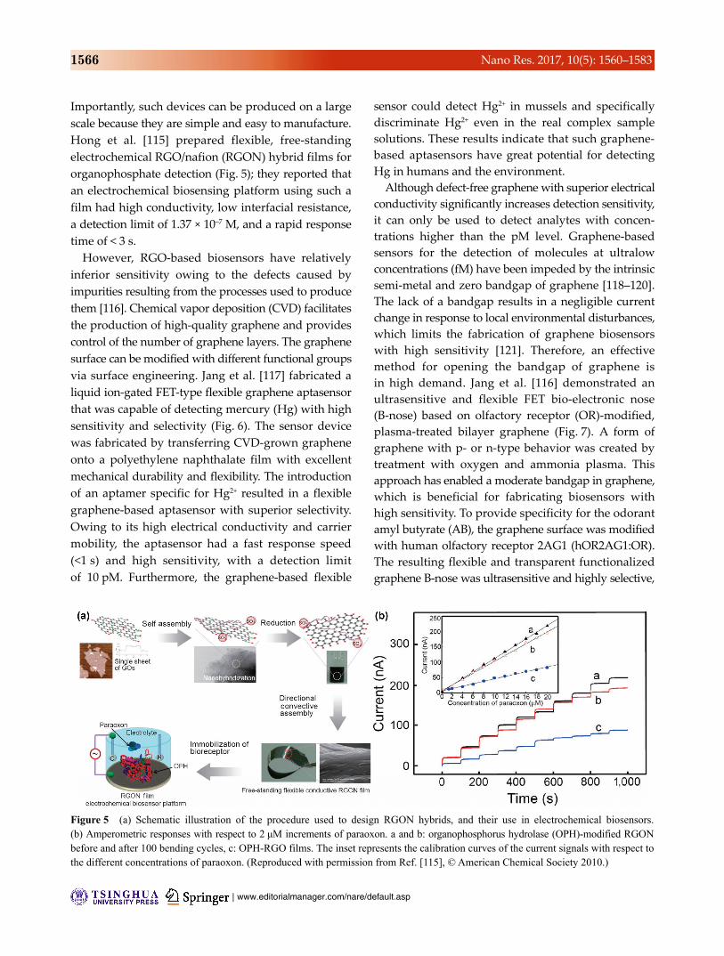
Hong et al. [115] prepared flexible, free-standing
electrochemical RGO/nafion (RGON) hybrid films for
organophosphate detection (Fig. 5); they reported that
an electrochemical biosensing platform using such a
film had high conductivity, low interfacial resistance,
a detection limit of 1.37 × 10‒7 M, and a rapid response
time of < 3 s.
However, RGO-based biosensors have relatively
inferior sensitivity owing to the defects caused by
impurities resulting from the processes used to produce
them [116]. Chemical vapor deposition (CVD) facilitates
the production of high-quality graphene and provides
control of the number of graphene layers. The graphene
surface can be modified with different functional groups
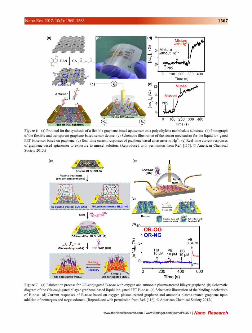
via surface engineering. Jang et al. [117] fabricated a
liquid ion-gated FET-type flexible graphene aptasensor
that was capable of detecting mercury (Hg) with high
sensitivity and selectivity (Fig. 6). The sensor device
was fabricated by transferring CVD-grown graphene
onto a polyethylene naphthalate film with excellent
mechanical durability and flexibility. The introduction
of an aptamer specific for Hg2+ resulted in a flexible
graphene-based aptasensor with superior selectivity.
Owing to its high electrical conductivity and carrier
mobility, the aptasensor had a fast response speed
(<1 s) and high sensitivity, with a detection limit
of 10 pM. Furthermore, the graphene-based flexible
sensor could detect Hg2+ in mussels and specifically
discriminate Hg2+ even in the real complex sample
solutions. These results indicate that such graphene-
based aptasensors have great potential for detecting
Hg in humans and the environment.
Although defect-free graphene with superior electrical
conductivity significantly increases detection sensitivity,
it can only be used to detect analytes with concen-
trations higher than the pM level. Graphene-based
sensors for the detection of molecules at ultralow
concentrations (fM) have been impeded by the intrinsic
semi-metal and zero bandgap of graphene [118‒120].
The lack of a bandgap results in a negligible current
change in response to local environmental disturbances,
which limits the fabrication of graphene biosensors
with high sensitivity [121]. Therefore, an effective
method for opening the bandgap of graphene is
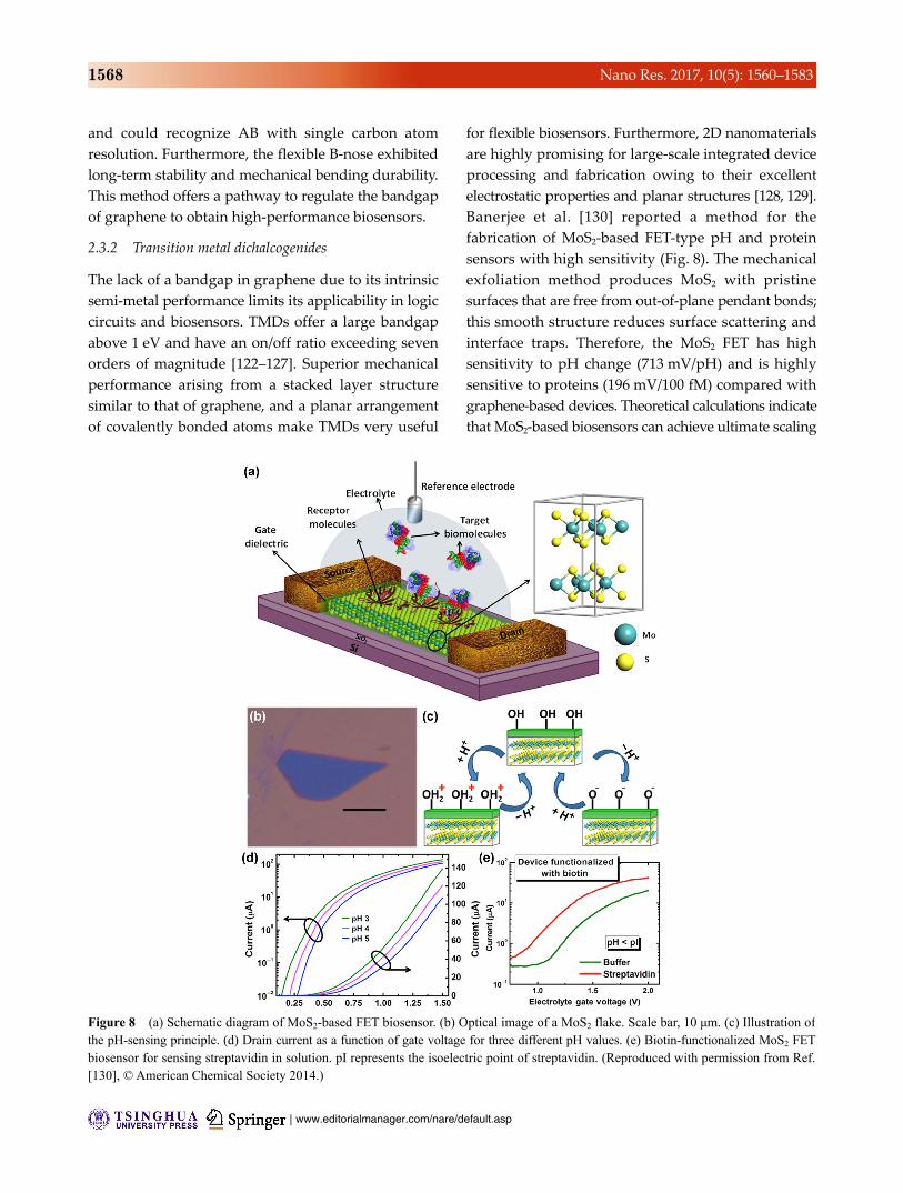
in high demand. Jang et al. [116] demonstrated an
ultrasensitive and flexible FET bio-electronic nose
(B-nose) based on olfactory receptor (OR)-modified,
plasma-treated bilayer graphene (Fig. 7). A form of
graphene with p- or n-type behavior was created by
treatment with oxygen and ammonia plasma. This
approach has enabled a moderate bandgap in graphene,
which is beneficial for fabricating biosensors with
high sensitivity. To provide specificity for the odorant
amyl butyrate (AB), the graphene surface was modified
with human olfactory receptor 2AG1 (hOR2AG1:OR).
The resulting flexible and transparent functionalized
graphene B-nose was ultrasensitive and highly selective,
Figure 5 (a) Schematic illustration of the procedure used to design RGON hybrids, and their use in electrochemical biosensors.(b) Amperometric responses with respect to 2 μM increments of paraoxon. a and b: organophosphorus hydrolase (OPH)-modified RGONbefore and after 100 bending cycles, c: OPH-RGO films. The inset represents the calibration curves of the current signals with respect to the different concentrations of paraoxon. (Reproduced with permission from Ref. [115], © American Chemical Society 2010.)
www.theNanoResearch.com∣www.Springer.com/journal/12274 | Nano Research
1567 Nano Res. 2017, 10(5): 1560–1583
Figure 6 (a) Protocol for the synthesis of a flexible graphene-based aptasensor on a polyethylene naphthalate substrate. (b) Photograph of the flexible and transparent graphene-based sensor device. (c) Schematic illustration of the sensor mechanism for the liquid ion-gated FET biosensor based on graphene. (d) Real-time current responses of graphene-based aptasensor to Hg2+. (e) Real-time current responsesof graphene-based aptasensor to exposure to mussel solution. (Reproduced with permission from Ref. [117], © American Chemical Society 2013.)
Figure 7 (a) Fabrication process for OR-conjugated B-nose with oxygen and ammonia plasma-treated bilayer graphene. (b) Schematic diagram of the OR-conjugated bilayer graphene-based liquid ion-gated FET B-nose. (c) Schematic illustration of the binding mechanism of B-nose. (d) Current responses of B-nose based on oxygen plasma-treated graphene and ammonia plasma-treated graphene upon addition of nontargets and target odorant. (Reproduced with permission from Ref. [116], © American Chemical Society 2012.)
| www.editorialmanager.com/nare/default.asp
1568 Nano Res. 2017, 10(5): 1560–1583
and could recognize AB with single carbon atom
resolution. Furthermore, the flexible B-nose exhibited
long-term stability and mechanical bending durability.
This method offers a pathway to regulate the bandgap
of graphene to obtain high-performance biosensors.
2.3.2 Transition metal dichalcogenides
The lack of a bandgap in graphene due to its intrinsic
semi-metal performance limits its applicability in logic
circuits and biosensors. TMDs offer a large bandgap
above 1 eV and have an on/off ratio exceeding seven
orders of magnitude [122‒127]. Superior mechanical
performance arising from a stacked layer structure
similar to that of graphene, and a planar arrangement
of covalently bonded atoms make TMDs very useful
for flexible biosensors. Furthermore, 2D nanomaterials
are highly promising for large-scale integrated device
processing and fabrication owing to their excellent
electrostatic properties and planar structures [128, 129].
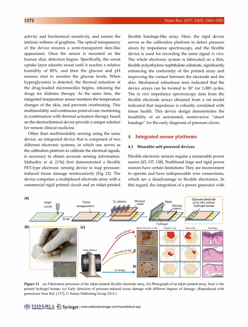
Banerjee et al. [130] reported a method for the
fabrication of MoS2-based FET-type pH and protein
sensors with high sensitivity (Fig. 8). The mechanical
exfoliation method produces MoS2 with pristine
surfaces that are free from out-of-plane pendant bonds;
this smooth structure reduces surface scattering and
interface traps. Therefore, the MoS2 FET has high
sensitivity to pH change (713 mV/pH) and is highly
sensitive to proteins (196 mV/100 fM) compared with
graphene-based devices. Theoretical calculations indicate
that MoS2-based biosensors can achieve ultimate scaling
Figure 8 (a) Schematic diagram of MoS2-based FET biosensor. (b) Optical image of a MoS2 flake. Scale bar, 10 μm. (c) Illustration of the pH-sensing principle. (d) Drain current as a function of gate voltage for three different pH values. (e) Biotin-functionalized MoS2 FETbiosensor for sensing streptavidin in solution. pI represents the isoelectric point of streptavidin. (Reproduced with permission from Ref. [130], © American Chemical Society 2014.)

www.theNanoResearch.com∣www.Springer.com/journal/12274 | Nano Research
1569 Nano Res. 2017, 10(5): 1560–1583
limits while retaining high sensitivity. Ultrathin MoS2
nanosheets are highly transparent, flexible, and
mechanically strong. 2D TMDs can be used in wearable
and implantable biosensors by interfacing the nano-
material with flexible substrates. However, the practical
application of 2D TMDs in flexible biosensors is
problematic because the high temperatures involved
in their fabrication may lead to the decomposition of
the substrates. Furthermore, carrier mobility on flexible
substrates is lower than on Si substrates.
2.4 Composites
The formation of hybrid nanostructures can com-
pensate for the shortcomings of a single material. For
instance, graphene/silver nanowire hybrid films not
only overcome the limitations of nanowire-percolating
networks by decreasing their pattern sizes, the weakness
of the nanowire against electrical breakdown, and
chemical oxidation, but also decrease the relatively
high sheet resistance of graphene [131]. In fluidic
sensing devices, pristine graphene has structural
limitations such as structural unreliability, irregular
active areas, poor adhesion of the fluidic modules,
and low sensitivity and selectivity. Therefore, novel
technologies for advanced graphene-based hybrids
are needed for fabricating high-performance flexible
electronics. Lee et al. [132] reported a novel FET
biosensor based on RGO-encapsulated nanoparticles
for the selective and sensitive detection of key
biomarkers of breast cancer. These well-organized 2D
or 3D graphene nanostructures with high surface-to-
volume ratios can generate 3D electrical surfaces,
improving detection limits and facilitating the highly
reproducible detection of important biomarkers.
The combination of graphene and nanoparticles
provides enlarged active areas that interact with
analytes and have a stable sensing geometry. Duan
et al. [133] fabricated a new type of flexible electro-
chemical sensor by depositing high-density Pt nano-
particles on RGO-carrying MnO2 nanowire networks
(Fig. 9). In this well-organized system, RGO serves as
the mechanical support and provides high electrical
Figure 9 (a) Fabrication of a biosensor system with paper-based electrodes. (b) Optical photographs of the GO and RGO paper.(c) Amperometric responses of the Pt-MnO2/RGO paper electrode with the addition of fMLP and catalase in the absence (upper) andpresence (bottom) of HepG2 cells. Inset, microscopy image of HepG2 cells. (Reproduced with permission from Ref. [133], © John Wiley & Sons 2012.)

| www.editorialmanager.com/nare/default.asp
1570 Nano Res. 2017, 10(5): 1560–1583
conductivity, MnO2 networks have a high surface area,
and Pt nanoparticles have superior catalytic activity.
Consequently, the device demonstrated significantly
improved sensitivity and selectivity when it was used
for the non-enzymatic detection of H2O2 secreted by
live cells. Jang et al. [134] constructed novel liquid
ion-gated FET flexible HIV immunoassays using
large-scale graphene micropattern (GM) nanobiohybrids
with close-packed carboxylated polypyrrole nano-
particle (cPPyNP) arrays (Fig. 10). Size-controllable
graphene micropatterns facilitate the accurate and
reliable production of fluidic systems. Owing to
the synergistic effect of graphene and the conducting
polymer, a nano-biohybrid HIV immunosensor exhibits
an unprecedentedly low detection limit of 1 pM.
Furthermore, the nano-biohybrid sensor also has
excellent mechanical bendability and durability.
3 Device designs
Previously, the developers of flexible biosensors mostly
focused on the design of high-sensitivity biosensors
with a single modality in which the sensor only
measures a unique sensing parameter under a single
stimulus. However, in real biological systems multiple
variations exist in the micro-environment. Therefore,
bio-electronics must be designed to provide multimo-
dality in sensing multiple stimuli. Kim et al. [135]
reported a graphene-based wearable electrochemical
device for diabetes monitoring and feedback therapy
(Fig. 11). The device consists of a sensor system that
is composed of temperature, humidity, glucose, and
pH sensors. It also includes a therapy system that
comprises a heater and polymeric microneedles,
which can be thermally activated to deliver drugs
transcutaneously. The large-area stretchable device
comprises a bilayer of gold mesh and gold-doped
graphene with high electrical conductivity and
mechanical reliability, which provides the major
electrochemical interface for the stable transfer of
electrical signals. The sensor for detecting multiple
stimuli is produced by selective functionalization of
the gold-doped graphene with electrochemically active
and soft materials, which enhances the electrochemical
Figure 10 (a) Protocol for the fabrication of flexible FET-type GM nano-biohybrid immunosensor based on GMs conjugated with close-packed CPPyNPs. (b) Schematic illustration of GM nano-biohybrid-based immunosensors (GMNS) operated by liquid gating. (c) Real-time current responses of GM, CPPy-GM, HIV-2 Ag-GM, and GMNS upon exposure to different HIV-2 gp36 Ab concentrations. (d) Current responses of the flexible FET-type GMNS to different HIV-2 gp36 Ab concentrations. (Reproduced with permission from Ref. [134], © John Wiley & Sons 2013.)

www.theNanoResearch.com∣www.Springer.com/journal/12274 | Nano Research
1571 Nano Res. 2017, 10(5): 1560–1583
Figure 11 (a) Schematic representation of the diabetes patch with various functional components such as sweat-control, sensing, and therapy systems. (b) Optical camera images of the diabetes patch deposited on human skin with various mechanical deformations.(c) Optical image of a portable electrochemical system connected to the wearable diabetes monitoring and therapy system. (d) Relativehumidity measurement by the diabetes patch. (e) Real-time detection of glucose in human sweat and blood with the diabetes patch.(f) Optical image of the heater integrated with microneedles deposited on mouse skin. (g) Optical images of the mouse skin withmicro-sized holes. (Reproduced with permission from Ref. [135], © Nature Publishing Group 2016.)
| www.editorialmanager.com/nare/default.asp
1572 Nano Res. 2017, 10(5): 1560–1583
activity and biochemical sensitivity, and retains the
intrinsic softness of graphene. The optical transparency
of the device ensures a semi-transparent skin-like
appearance. Once the sensor is mounted on the
human skin, detection begins. Specifically, the sweat
uptake layer adsorbs sweat until it reaches a relative
humidity of 80%, and then the glucose and pH
sensors start to monitor the glucose levels. When
hyperglycemia is detected, the thermal actuation of
the drug-loaded microneedles begins, releasing the
drugs for diabetes therapy. At the same time, the
integrated temperature sensor monitors the temperature
changes of the skin, and prevents overheating. This
multimodality and continuous point-of-care monitoring
in combination with thermal actuation therapy based
on the electrochemical device provide a unique solution
for remote clinical medicine.
Other than multimodality sensing using the same
device, an integrated device that is composed of two
different electronic systems, in which one serves as
the calibration platform to calibrate the electrical signals,
is necessary to obtain accurate sensing information.
Maharbiz et al. [136] first demonstrated a flexible
FET-type electronic sensing device to map pressure-
induced tissue damage noninvasively (Fig. 12). The
device comprises a multiplexed electrode array with a
commercial rigid printed circuit and an inkjet-printed
flexible bandage-like array. Here, the rigid device
serves as the calibration platform to detect pressure
ulcers by impedance spectroscopy, and the flexible
device is used for recording the same signal in vivo.
The whole electronic system is fabricated on a thin,
flexible polyethylene naphthalate substrate, significantly
enhancing the conformity of the printed array and
improving the contact between the electrode and the
skin. Mechanical robustness tests indicated that the
device arrays can be twisted to 30° for 1,000 cycles.
The in vivo impedance spectroscopy data from the
flexible electrode arrays obtained from a rat model
indicated that impedance is robustly correlated with
tissue health. This device design demonstrates the
feasibility of an automated, noninvasive “smart
bandage” for the early diagnosis of pressure ulcers.
4 Integrated sensor platforms
4.1 Wearable self-powered devices
Flexible electronic sensors require a sustainable power
source [43, 137, 138]. Traditional large and rigid power
sources have certain limitations: They are inconvenient
to operate and have indispensable wire connections,
which are a disadvantage in flexible electronics. In
this regard, the integration of a power generator with
Figure 12 (a) Fabrication processes of the inkjet printed flexible electrode array. (b) Photograph of an inkjet printed array. Inset is theprinted hydrogel bumps. (c) Early detection of pressure-induced tissue damage with different degrees of damage. (Reproduced with permission from Ref. [137], © Nature Publishing Group 2015.)
www.theNanoResearch.com∣www.Springer.com/journal/12274 | Nano Research
1573 Nano Res. 2017, 10(5): 1560–1583
a flexible biosensor is an efficient design for wearable
self-powered devices. The mechanical energy derived
from various stretching motions is a cost-effective
and highly efficient approach to energy harvesting.
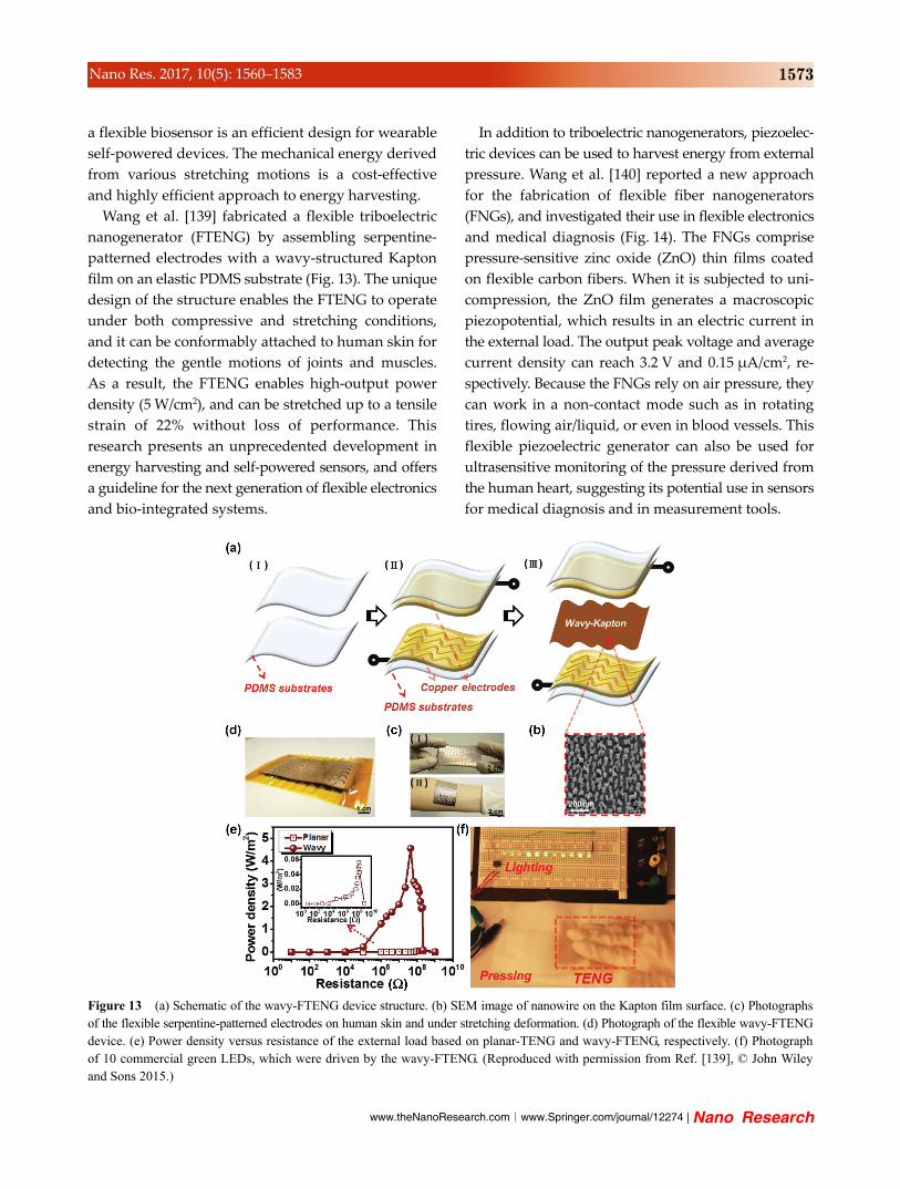
Wang et al. [139] fabricated a flexible triboelectric
nanogenerator (FTENG) by assembling serpentine-
patterned electrodes with a wavy-structured Kapton
film on an elastic PDMS substrate (Fig. 13). The unique
design of the structure enables the FTENG to operate
under both compressive and stretching conditions,
and it can be conformably attached to human skin for
detecting the gentle motions of joints and muscles.
As a result, the FTENG enables high-output power
density (5 W/cm2), and can be stretched up to a tensile
strain of 22% without loss of performance. This
research presents an unprecedented development in
energy harvesting and self-powered sensors, and offers
a guideline for the next generation of flexible electronics
and bio-integrated systems.
In addition to triboelectric nanogenerators, piezoelec-
tric devices can be used to harvest energy from external
pressure. Wang et al. [140] reported a new approach
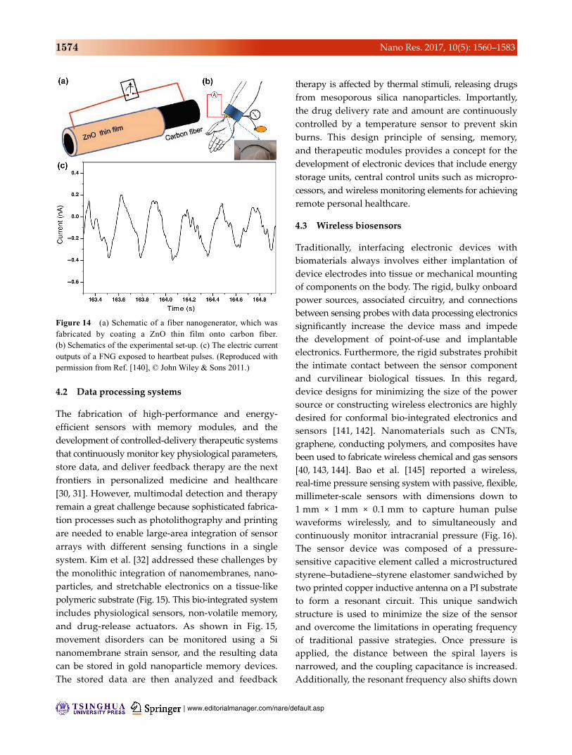
for the fabrication of flexible fiber nanogenerators
(FNGs), and investigated their use in flexible electronics
and medical diagnosis (Fig. 14). The FNGs comprise
pressure-sensitive zinc oxide (ZnO) thin films coated
on flexible carbon fibers. When it is subjected to uni-
compression, the ZnO film generates a macroscopic
piezopotential, which results in an electric current in
the external load. The output peak voltage and average
current density can reach 3.2 V and 0.15 μA/cm2, re-
spectively. Because the FNGs rely on air pressure, they
can work in a non-contact mode such as in rotating
tires, flowing air/liquid, or even in blood vessels. This
flexible piezoelectric generator can also be used for
ultrasensitive monitoring of the pressure derived from
the human heart, suggesting its potential use in sensors
for medical diagnosis and in measurement tools.
Figure 13 (a) Schematic of the wavy-FTENG device structure. (b) SEM image of nanowire on the Kapton film surface. (c) Photographsof the flexible serpentine-patterned electrodes on human skin and under stretching deformation. (d) Photograph of the flexible wavy-FTENGdevice. (e) Power density versus resistance of the external load based on planar-TENG and wavy-FTENG, respectively. (f) Photograph of 10 commercial green LEDs, which were driven by the wavy-FTENG. (Reproduced with permission from Ref. [139], © John Wiley and Sons 2015.)
| www.editorialmanager.com/nare/default.asp
1574 Nano Res. 2017, 10(5): 1560–1583
Figure 14 (a) Schematic of a fiber nanogenerator, which was fabricated by coating a ZnO thin film onto carbon fiber. (b) Schematics of the experimental set-up. (c) The electric current outputs of a FNG exposed to heartbeat pulses. (Reproduced with permission from Ref. [140], © John Wiley & Sons 2011.)
4.2 Data processing systems
The fabrication of high-performance and energy-
efficient sensors with memory modules, and the
development of controlled-delivery therapeutic systems
that continuously monitor key physiological parameters,
store data, and deliver feedback therapy are the next
frontiers in personalized medicine and healthcare
[30, 31]. However, multimodal detection and therapy
remain a great challenge because sophisticated fabrica-
tion processes such as photolithography and printing
are needed to enable large-area integration of sensor
arrays with different sensing functions in a single
system. Kim et al. [32] addressed these challenges by
the monolithic integration of nanomembranes, nano-
particles, and stretchable electronics on a tissue-like
polymeric substrate (Fig. 15). This bio-integrated system
includes physiological sensors, non-volatile memory,
and drug-release actuators. As shown in Fig. 15,
movement disorders can be monitored using a Si
nanomembrane strain sensor, and the resulting data
can be stored in gold nanoparticle memory devices.
The stored data are then analyzed and feedback
therapy is affected by thermal stimuli, releasing drugs
from mesoporous silica nanoparticles. Importantly,
the drug delivery rate and amount are continuously
controlled by a temperature sensor to prevent skin
burns. This design principle of sensing, memory,
and therapeutic modules provides a concept for the
development of electronic devices that include energy
storage units, central control units such as micropro-
cessors, and wireless monitoring elements for achieving
remote personal healthcare.
4.3 Wireless biosensors
Traditionally, interfacing electronic devices with
biomaterials always involves either implantation of
device electrodes into tissue or mechanical mounting
of components on the body. The rigid, bulky onboard
power sources, associated circuitry, and connections
between sensing probes with data processing electronics
significantly increase the device mass and impede
the development of point-of-use and implantable
electronics. Furthermore, the rigid substrates prohibit
the intimate contact between the sensor component
and curvilinear biological tissues. In this regard,
device designs for minimizing the size of the power
source or constructing wireless electronics are highly
desired for conformal bio-integrated electronics and
sensors [141, 142]. Nanomaterials such as CNTs,
graphene, conducting polymers, and composites have
been used to fabricate wireless chemical and gas sensors
[40, 143, 144]. Bao et al. [145] reported a wireless,
real-time pressure sensing system with passive, flexible,
millimeter-scale sensors with dimensions down to
1 mm × 1 mm × 0.1 mm to capture human pulse
waveforms wirelessly, and to simultaneously and
continuously monitor intracranial pressure (Fig. 16).
The sensor device was composed of a pressure-
sensitive capacitive element called a microstructured
styrene–butadiene–styrene elastomer sandwiched by
two printed copper inductive antenna on a PI substrate
to form a resonant circuit. This unique sandwich
structure is used to minimize the size of the sensor
and overcome the limitations in operating frequency
of traditional passive strategies. Once pressure is
applied, the distance between the spiral layers is
narrowed, and the coupling capacitance is increased.
Additionally, the resonant frequency also shifts down

www.theNanoResearch.com∣www.Springer.com/journal/12274 | Nano Research
1575 Nano Res. 2017, 10(5): 1560–1583
Figure 15 (a) Wearable electronic patch with data storage modules, diagnostic tools, and therapeutic actuating elements. (b) Optical imageof the wearable bio-integrated system. (c) Current versus voltage characteristics with compliance currents below ~100 µA. (d) Schematic representation of the controlled transdermal drug delivery patch. (e) Temperature distribution of the heater on the skin patch. (Reproducedwith permission from Ref. [32], © Nature Publishing Group 2014.)
Figure 16 (a) Structure design of the resonant sensor device. (b) Photograph of the pyramidal-structured SBS dielectric. (c) Photograph of the 2-turn devices with different dimensions. (d) Wireless monitoring with the sensor implanted in mouse. (e) The sensor resonant peak in the measured group delay distortion (GDD) spectrum under no applied air pressure, saline, and mouse. (f) Measured pressurewaveforms after performing abdominal compression on mouse. An external reference sensor was also used. Arrows indicate when compression was applied. (Reproduced with permission from Ref. [145], © Nature Publishing Group 2014.)
| www.editorialmanager.com/nare/default.asp
1576 Nano Res. 2017, 10(5): 1560–1583
to lower frequencies under a specific pressure. This
uniquely designed small and flexible device with
improved mechanical robustness allows the intimate
connection of sensors with biomaterials. The wireless
sensor arrays can continuously capture human pulse
waveforms in vivo with high sensitivity, and can obtain
concurrent spatial pressure mapping. This fabrication
technology has enabled a range of applications in
continuous and wireless detection of various important
physiological parameters for biomedical research and
human healthcare.
5 Issues and challenges
Despite the outstanding properties of nanostructured
material for advanced bio-electronics and integrated
devices, it is prudent to give a comprehensive discussion
of the challenges that flexible electronics have faced.
In terms of the material synthesis, the exploration of
a large-scale and highly efficient approach towards
patterned nanomaterials is of vital importance for the
fabrication of flexible devices with high sensitivity
and reproducibility. However, the engineering of 0D
nanomaterials with superior contact to improve
the conductivity and reduce the power consumption
remains a practical challenge. Interconnected 1D
nanomaterials exhibit high conductivity, even when
stretched. However, nanowires are not widely utilized
in devices owing to the limitations of reproducibility
and stability [146‒148]. High-performance nanowire-
based devices always require complex and difficult
fabrication processes. More importantly, for practical
flexible nanoelectronics, the large area pattering of
2D thin films and devices on flexible substrates is an
essential prerequisite. Though some techniques based
on sheet and roll-to-roll processing for large-area
nanotechnology have been explored, obtaining large-
area and high-quality 2D nanomaterials has significantly
impeded the commercialization of the current flexible
devices [149‒151].
The surface modifications of nanomaterials with
specific recognition elements are convincing solutions
to satisfy the required selectivity, sensitivity, and
stability of biosensors. Thus, surface modification
technologies that do not influence the electronic and
physical performance of nanomaterials are desired.
The long-term toxicity analysis of nanomaterials is
also critical for invasive bioelectronics. In addition,
the selectivity and long-term stability of biosensors in
practical or complex environments must be considered.
The engineering of functionalized nanomaterial arrays
to facilitate the fabrication of multifunctional microchips
for highly efficient, sensitive, and selective sensing are
of critical importance for real-time analysis. It is worth
mentioning that the surface functionalization of nano-
materials to provide hydrophilicity can also significantly
enhance the contact between the device and bio-
materials, and thus improve biosensing performance.
In real-life applications of flexible biosensors for
disease diagnosis, the exploitation of integrated systems
such as the combination of physical and chemical or
biological sensors for monitoring multiplex motions
and disease biomarkers are essential. In particular,
the integration of sensors with data storage systems
and transmission systems for long-term and continuous
monitoring, delivering signals to an instrument for
further analysis, transferring feedback information to
humans, and providing the corresponding therapies
is a goal for personal healthcare. However, the com-
bination of each device component to realize fully
integrated flexible bio-electronics remains a challenge.
More importantly, the sophisticated preparation pro-
cedures involving photolithography and printing to
obtain large-area sensor arrays, power sources, and
wireless monitoring systems remains to be addressed
for practical implementation. Currently developed
energy harvesting and storage devices that provide
the energy to power electronic devices are typically
heavy owing to the presence of bulk and rigid cell
encapsulation material. The mass loading of active
material in electrodes must be kept at a relatively
high value to obtain high energy and power density,
which significantly impedes the realization of trans-
parent batteries [152‒157]. Therefore, it is difficult to
integrate energy storage systems with whole bio-
electronics because flexible and wearable bio-electronics
require characteristics such as low weight and trans-
parency. Although devices that provide detection and
therapy facilitate a pathway for point-of-care medicine,
the low drug loading capacity of such devices makes
disease therapy difficult [32, 135]. Furthermore, detection
and therapy devices that can only be used once
www.theNanoResearch.com∣www.Springer.com/journal/12274 | Nano Research
1577 Nano Res. 2017, 10(5): 1560–1583
owing to the difficulty of cleaning the device surface,
significantly increase the fabrication costs.
6 Conclusions and outlook
Over the past decade, advances in nanostructured
materials, mechanical analysis, surface engineering,
device design, and nanofabrication techniques have
accelerated the development of flexible bio-electronics.
We have summarized the most recent developments
in flexible biosensors from the perspective of various
nanostructured nanomaterials and integrated device
systems. This review will provide researchers with
information on material selection, sensor fabrication,
data processing, and power requirements for flexible
biosensors. However, there are several remaining
challenges for the effective integration of these nano-
materials with soft substrates to obtain flexible bio-
electronics. The optimization of material fabrication
and modification techniques to obtain large-area,
high quality, and uniform arrays is essential for the
fabrication of highly sensitive and reproducible
biosensors. The exploration of small energy storage
and conversion devices with high energy and power
density, and optical transparency is important for
the development of high-performance bio-electronics.
Furthermore, device integration should be optimized
to minimize the whole device volume for implantable
electronics and point-of-care healthcare.
Acknowledgements
This work was supported by the National Natural
Science Foundation of China (Nos. 51272186, 21422105,
and 21675120), the Foundation for the Author of
National Excellent Doctoral Dissertation of PR China
(No. 201220), and Ten Thousand Talents Program for
Young Talents.
References
[1] Gao, W.; Emaminejad, S.; Nyein, H. Y. Y.; Challa, S.;
Chen, K.; Peck, A.; Fahad, H. M.; Ota, H.; Shiraki, H.;
Kiriya, D. et al. Fully integrated wearable sensor arrays for
multiplexed in situ perspiration analysis. Nature 2016, 529,
509–526.
[2] Tee, B. C.-K.; Wang, C.; Allen, R.; Bao, Z. N. An electrically
and mechanically self-healing composite with pressure- and
flexion-sensitive properties for electronic skin applications.
Nat. Nanotechnol. 2012, 7, 825–832.
[3] Park, S.; Wang, G.; Cho, B.; Kim, Y.; Song, S.; Ji, Y.;
Yoon, M.-H.; Lee, T. Flexible molecular-scale electronic
devices. Nat. Nanotechnol. 2012, 7, 438–442.
[4] Trung, T. Q.; Lee N.-E. Flexible and stretchable physical
sensor integrated platforms for wearable human-activity
monitoring and personal healthcare. Adv. Mater. 2016, 28,
4338–4372.
[5] Viventi, J.; Kim, D.-H.; Vigeland, L.; Frechette, E. S.;
Blanco, J. A.; Kim, Y.-S.; Avrin, A. E.; Tiruvadi, V. R.;
Hwang, S.-W.; Vanleer, A. C. et al. Flexible, foldable,
actively multiplexed, high-density electrode array for mapping
brain activity in vivo. Nat. Neurosci. 2011, 14, 1599–1607.
[6] Nguyen, T. D.; Deshmukh, N.; Nagarah, J. M.; Kramer, T.;
Purohit, P. K.; Berry M. J.; McAlpine, M. C. Piezoelectric
nanoribbons for monitoring cellular deformations. Nat.
Nanotechnol. 2012, 7, 587–593.
[7] Rim, Y. S.; Bae, S.-H.; Chen, H. J.; De Marco, N.; Yang, Y.
Recent progress in materials and devices toward printable
and flexible sensors. Adv. Mater. 2016, 28, 4415–4440.
[8] Khan, Y.; Ostfeld, A. E.; Lochner, C. M.; Pierre, A.; Arias,
A. C. Monitoring of vital signs with flexible and wearable
medical devices. Adv. Mater. 2016, 28, 4373–4395.
[9] Salvatore, G. A.; Münzenrieder, N.; Kinkeldei, T.; Petti, L.;
Zysset, C.; Strebel, I.; Büthe, L.; Tröster, G. Wafer-scale
design of lightweight and transparent electronics that wraps
around hairs. Nat. Commun. 2014, 5, 2982.
[10] Mannsfeld, S. C. B.; Tee, B. C.-K.; Stoltenberg, R. M.;
Chen, C. V. H.-H.; Barman, S.; Muir, B. V. O.; Sokolov, A.
N. Reese, C.; Bao, Z. N. Highly sensitive flexible pressure
sensors with microstructured rubber dielectric layers. Nat.
Mater. 2010, 9, 859–864.
[11] Lee, S.; Reuveny, A.; Reeder, J.; Lee, S.; Jin, H.; Liu,
Q. H.; Yokota, T.; Sekitani, T.; Isoyama, T.; Abe, Y. et al.
A transparent bending-insensitive pressure sensor. Nat.
Nanotechnol. 2016, 11, 472–478.
[12] Ramuz, M.; Tee, B. C.-K.; Tok, J. B.-H.; Bao, Z. N.
Transparent, optical, pressure-sensitive artificial skin for
large-area stretchable electronics. Adv. Mater. 2012, 24,
3223–3227.
[13] Jung, S.; Lee, J.; Hyeon, T.; Lee, M.; Kim, D.-H. Fabric-
based integrated energy devices for wearable activity monitors.
Adv. Mater. 2014, 26, 6329–6334.
[14] Pang, C.; koo, J. H.; Nguyen, A.; Caves, J. M.; Kim, M.-G.;
Chortos, A.; Kim, K.; Wang, P. J.; Tok, J. B.-H.; Bao, Z. N.
Highly skin-conformal microhairy sensor for pulse signal
amplification. Adv. Mater. 2015, 27, 634–640.
| www.editorialmanager.com/nare/default.asp
1578 Nano Res. 2017, 10(5): 1560–1583
[15] Kim, J.; Lee, M.; Shim, H. J.; Ghaffari, R.; Cho, H. R.;
Son, D.; Jung, Y. H.; Soh, M.; Choi, C.; Jung, S. et al.
Stretchable silicon nanoribbon electronics for skin prosthesis.
Nat. Commun. 2014, 5, 5747.
[16] Kim, R.-H.; Kim, D.-H.; Xiao, J. L.; Kim, B. H.; Park, S.-I.;
Panilaitis, B.; Ghaffari, R.; Yao, J. M.; Li, M.; Liu, Z. J.
et al. Waterproof AlInGaP optoelectronics on stretchable
substrates with applications in biomedicine and robotics.
Nat. Mater. 2010, 9, 929–937.
[17] Guo, Y. L.; Wu, B.; Liu, H. T.; Ma, Y. Q.; Yang, Y.;
Zheng, J.; Gui, Y.; Liu, Y. Q. Electrical assembly and
reduction of graphene oxide in a single solution step for use
in flexible sensors. Adv. Mater. 2011, 23, 4626–4630.
[18] Dong, X. C.; Shi, Y. M.; Huang, W.; Chen, P.; Li, L.-J.
Electrical detection of DNA hybridization with single-base
specificity using transistors based on CVD-grown graphene
sheets. Adv. Mater. 2010, 22, 1649–1653.
[19] Xu, G. Y.; Abbott, J.; Qin, L.; Yeung, K. Y. M.; Song, Y.;
Yoon, H. S.; Kong, J.; Ham, D. Electrophoretic and field-
effect graphene for all-electrical DNA array technology. Nat.
Commun. 2014, 5, 4866.
[20] He, Q. Y.; Sudibya, H. G.; Yin, Z. Y.; Wu, S. X.; Li, H.;
Boey, F.; Huang, W.; Chen, P.; Zhang, H. Centimeter-long
and large-scale micropatterns of reduced graphene oxide
films: Fabrication and sensing applications. ACS Nano 2010,
4, 3201–3208.
[21] Feng, L. Y.; Chen, Y.; Ren, J. S.; Qu, X. G. A graphene
functionalized electrochemical aptasensor for selective label-
free detection of cancer cells. Biomaterials 2011, 32, 2930–
2937.
[22] Zhang, M.; Liao, C. Z.; Mak, C. H.; You, P.; Mak, C. L.;
Yan, F. Highly sensitive glucose sensors based on enzyme-
modified whole-graphene solution-gated transistors. Sci. Rep.
2015, 5, 8311.
[23] Zhang, M.; Liao, C. Z.; Yao, Y. L.; Liu, Z. K.; Gong, F. F.;
Yan, F. High-performance dopamine sensors based on whole-
graphene solution-gated transistors. Adv. Funct. Mater. 2014,
24, 978–985.
[24] Yan, F.; Zhang, M.; Li, J. H. Solution-gated graphene
transistors for chemical and biological sensors. Adv. Healthc.
Mater. 2014, 3, 313–331.
[25] Deng, W.; Zhang, X. J.; Huang, L. M.; Xu, X. Z.; Wang, L.;
Wang, J. C.; Shang, Q. X.; Lee, S.-T.; Jie, J. S. Aligned
single-crystalline perovskite microwire arrays for high-
performance flexible image sensors with long-term stability.
Adv. Mater. 2016, 28, 2201–2208.
[26] Shin, S. R.; Farzad, R.; Tamayol, A.; Manoharan, V.;
Mostafalu, P.; Zhang, Y. S.; Akbari, M.; Jung, S. M.; Kim,
D.; Comotto, M. et al. A bioactive carbon nanotube-based
ink for printing 2D and 3D flexible electronics. Adv. Mater.
2016, 28, 3280–3289.
[27] Bhattacharyya, D.; Senecal, K.; Marek, P.; Senecal, A.;
Gleason, K. K. High surface area flexible chemiresistive
biosensor by oxidative chemical vapor deposition. Adv.
Funct. Mater. 2011, 21, 4328–4337.
[28] Baeg, K.-J.; Caironi, M.; Noh, Y.-Y. Toward printed
integrated circuits based on unipolar or ambipolar polymer
semiconductors. Adv. Mater. 2013, 25, 4210–4244.
[29] Chen, H. T.; Cao, Y.; Zhang, J. L.; Zhou, C. W. Large-scale
complementary macroelectronics using hybrid integration
of carbon nanotubes and IGZO thin-film transistors. Nat.
Commun. 2014, 5, 4097.
[30] Chen, H. L.; Cheng, N. Y.; Ma, W.; Li, M. L.; Hu, S. X.;
Gu, L.; Meng, S.; Guo, X. F. Design of a photoactive hybrid
bilayer dielectric for flexible nonvolatile organic memory
transistors. ACS Nano 2016, 10, 436–445.
[31] Kim, R. H.; Kim, H. J.; Bae, I.; Hwang, S. K.; Velusamy,
D. B.; Cho, S. M.; Takaishi, K.; Muto, T.; Hashizume, D.;
Uchiyama, M. et al. Non-volatile organic memory with sub-
millimetre bending radius. Nat. Commun. 2014, 5, 3583.
[32] Son, D.; Lee, J.; Qiao, S. T.; Ghaffari, R.; Kim, J.; Lee, J. E.;
Song, C.; Kim, S. J.; Lee, D. J.; Jun, S. W. et al.
Multifunctional wearable devices for diagnosis and therapy
of movement disorders. Nat. Nanotechnol. 2014, 9, 397–404.
[33] Irimia-Vladu, M.; Troshin, P. A.; Reisinger, M.; Shmygleva,
L.; Kanbur, Y.; Schwabegger, G.; Bodea, M.; Schwödiauer,
R.; Mumyatov, A.; Fergus, J. W. et al. Biocompatible and
biodegradable materials for organic field-effect transistors.
Adv. Funct. Mater. 2010, 20, 4069–4076.
[34] Takahashi, T.; Takei, K.; Gillies, A. G.; Fearing, R. S.;
Javey, A. Carbon nanotube active-matrix backplanes for
conformal electronics and sensors. Nano Lett. 2011, 11,
5408–5413.
[35] Lau, P. H.; Takei, K.; Wang, C.; Ju, Y.; Kim, J.; Yu, Z. B.;
Takahashi, T.; Cho, G.; Javey, A. Fully printed, high
performance carbon nanotube thin-film transistors on flexible
substrates. Nano Lett. 2013, 13, 3864–3869.
[36] Chae, S. H.; Yu, W. J.; Bae, J. J.; Duong, D. L.; Perello, D.;
Jeong, H. Y.; Ta, Q. H.; Ly, T. H.; Vu, Q. A.; Yun, M. et al.
Transferred wrinkled Al2O3 for highly stretchable and
transparent graphene–carbon nanotube transistors. Nat. Mater.
2013, 12, 403–409.
[37] Wang, X. W.; Gu, Y.; Xiong, Z. P.; Cui, Z.; Zhang, T.
Silk-molded flexible, ultrasensitive, and highly stable electronic
skin for monitoring human physiological signals. Adv. Mater.
2014, 26, 1336–1342.
[38] Segev-Bar, M.; Haick, H. Flexible sensors based on
nanoparticles. ACS Nano 2013, 7, 8366–8378.

www.theNanoResearch.com∣www.Springer.com/journal/12274 | Nano Research
1579 Nano Res. 2017, 10(5): 1560–1583
[39] Zhu, B. W.; Wang, H.; Leow, W. R.; Cai, Y. R.; Loh, X. J.;
Han, M.-Y.; Chen, X. D. Silk fibroin for flexible electronic
devices. Adv. Mater. 2016, 28, 4250–4265.
[40] Mannoor, M. S.; Tao, H.; Clayton, J. D.; Sengupta, A.;
Kaplan, D. L.; Naik, R. R.; Verma, N.; Omenetto, F. G.;
McAlphine, M. C. Graphene-based wireless bacteria detection
on tooth enamel. Nat. Commun. 2012, 3, 763.
[41] Lee, H.; Choi, T. K.; Lee, Y. B.; Cho, H. R.; Ghaffari, R.;
Wang, L.; Choi, H. J.; Chung, T. D.; Lu, N. S.; Hyeon, T.
et al. A graphene-based electrochemical device with
thermoresponsive microneedles for diabetes monitoring and
therapy. Nat. Nanotechnol. 2016, 11, 566–572.
[42] Swisher, S. L.; Lin, M. C.; Liao, A.; Leeflang, E. J.; Khan, Y.;
Pavinatto, F. J.; Mann, K.; Naujokas, A.; Young, D.; Roy, S.
et al. Impedance sensing device enables early detection of
pressure ulcers in vivo. Nat. Commun. 2015, 6, 6575.
[43] Wang, X. D.; Zhang, H. L.; Yu, R. M.; Dong, L.; Peng, D. F.;
Zhang, A. H.; Zhang, Y.; Liu, H.; Pan, C. F.; Wang, Z. L.
Dynamic pressure mapping of personalized handwriting by
a flexible sensor matrix based on the mechanoluminescence
process. Adv. Mater. 2015, 27, 2324–2331.
[44] Khodagholy, D.; Rivnay, J.; Sessolo, M.; Gurfinkel, M.;
Leleux, P.; Jimison, L. H.; Stavrinidou, E.; Herve, T.; Sanaur,
S.; Owens, R. M. et al. High transconductance organic
electrochemical transistors. Nat. Commun. 2013, 4, 2133.
[45] Rim, Y. S.; Bae, S.-H.; Chen, H. J.; Yang, J. L.; Kim, J.;
Andrews, A. M.; Weiss, P. S.; Yang, Y.; Tseng, H.-R.
Printable ultrathin metal oxide semiconductor-based conformal
biosensors. ACS Nano 2015, 9, 12174–12181.
[46] Liu, J.; Buchholz, B.; Chang, R. P. H.; Facchetti, A.; Marks,
T. J. High-performance flexible transparent thin-film transistors
using a hybrid gate dielectric and an amorphous zinc indium
tin oxide channel. Adv. Mater. 2010, 22, 2333–2337.
[47] Lu, X. H.; Zhai, T.; Zhang, X. H.; Shen, Y. Q.; Yuan, L. Y.;
Hu, B.; Gong, L.; Chen, J.; Gao, Y. H.; Zhou, J. et al.
WO3–x@Au@MnO2 core–shell nanowires on carbon fabric
for high-performance flexible supercapacitors. Adv. Mater.
2012, 24, 938–944.
[48] Lin, P.; Luo, X. T.; Hsing, I.-M.; Yan, F. Organic electro-
chemical transistors integrated in flexible microfluidic systems
and used for label-free DNA sensing. Adv. Mater. 2011, 23,
4035–4040.
[49] Bavykin, D. V.; Friedrich, J. M.; Walsh, F. C. Protonated
titanates and TiO2 nanostructured materials: Synthesis,
properties, and applications. Adv. Mater. 2006, 18, 2807–
2824.
[50] Wu, C. Z.; Wei, H.; Ning, B.; Xie, Y. New vanadium oxide
nanostructures: Controlled synthesis and their smart electrical
switching properties. Adv. Mater. 2010, 22, 1972–1976.
[51] Yan, J. Q.; Wang, T.; Wu, G. J.; Dai, W. L.; Guan, N. J.; Li,
L. D.; Gong, J. L. Tungsten oxide single crystal nanosheets
for enhanced multichannel solar light harvesting. Adv. Mater.
2015, 27, 1580–1586.
[52] Pradhan, D.; Noroui, F.; Leung, K. T. High-performance,
flexible enzymatic glucose biosensor based on ZnO nanowires
supported on a gold-coated polyester substrate. ACS Appl.
Mater. Interfaces 2010, 2, 2409–2412.
[53] Liu, X.; Gu, L. L.; Zhang, Q. P.; Wu, J. Y.; Long, Y. Z.;
Fan, Z. Y. All-printable band-edge modulated ZnO nanowire
photodetectors with ultra-high detectivity. Nat. Commun.
2014, 5, 4007.
[54] Kim, M.-G.; Kanatzidis, M. G.; Facchetti, A.; Marks, T. J.
Low-temperature fabrication of high-performance metal
oxide thin-film electronics via combustion processing. Nat.
Mater. 2011, 10, 382–388.
[55] Zhang, H.-X.; Feng, C.; Zhai, Y.-C.; Jiang, K.-L.; Li, Q.-Q.;
Fan, S.-S. Cross-stacked carbon nanotube sheets uniformly
loaded with SnO2 nanoparticles: A novel binder-free and
high-capacity anode material for lithium-ion batteries. Adv.
Mater. 2009, 21, 2299–2304.
[56] Vanithakumari, S. C.; Nanda, K. K. A one-step method
for the growth of Ga2O3-nanorod-based white-light-emitting
phosphors. Adv. Mater. 2009, 21, 3581–3584.
[57] Gong, S.; Schwalb, W.; Wang, Y. W.; Chen, Y.; Tang, Y.;
Si, J.; Shirinzadeh, B.; Cheng, W. L. A wearable and highly
sensitive pressure sensor with ultrathin gold nanowires. Nat.
Commun. 2014, 5, 3132.
[58] Yaman, M.; Khudiyev, T.; Ozgur, E.; Kanik, M.; Aktas, O.;
Ozgur, E. O.; Deniz, H.; Korkut, E.; Bayindir, M. Arrays of
indefinitely long uniform nanowires and nanotubes. Nat.
Mater. 2011, 10, 494–501.
[59] Tian, B. Z.; Liu, J.; Dvir, T.; Jin, L. H.; Tsui, J. H.; Qing, Q.;
Suo, Z. G.; Langer, R.; Kohane, D. S.; Lieber, C. M.
Macroporous nanowire nanoelectronic scaffolds for synthetic
tissues. Nat. Mater. 2012, 11, 986–994.
[60] Weisse, J. M.; KIm, D. R.; Lee, C. H.; Zheng, X. L.
Vertical transfer of uniform silicon nanowire arrays via
crack formation. Nano Lett. 2011, 11, 1300–1305.
[61] Xu, F.; Liu, W.; Zhu, Y. Controlled 3D buckling of silicon
nanowires for stretchable electronics. ACS Nano 2011, 5,
672–678.
[62] Jeon, D.-Y.; Pregl, S.; Park, S. J.; Baraban, L.; Cuniberti, G.;
Mikolajick, T.; Weber, W. M. Scaling and graphical
transport-map analysis of ambipolar schottky-barrier thin-
film transistors based on a parallel array of Si nanowires.
Nano Lett. 2015, 15, 4578–4584.
[63] Li, B.-R.; Hsieh, Y.-J.; Chen, Y.-X.; Chung, Y.-T.; Pan,
C.-Y.; Chen, Y.-T. An ultrasensitive nanowire-transistor
biosensor for detecting dopamine release from living PC12
cells under hypoxic stimulation. J. Am. Chem. Soc. 2013,

| www.editorialmanager.com/nare/default.asp
1580 Nano Res. 2017, 10(5): 1560–1583
135, 16034–16037.
[64] Kim, K. H.; Oh, Y.; Islam, M. F. Graphene coating makes
carbon nanotube aerogels superelastic and resistant to fatigue.
Nat. Nanotechnol. 2012, 7, 562–566.
[65] Shi, E. Z.; Li, H. B.; Yang, L.; Hou, J. F.; Li, Y. C.; Li, L.;
Cao, A. Y.; Fang, Y. Carbon nanotube network embroidered
graphene films for monolithic all-carbon electronics. Adv.
Mater. 2015, 27, 682–688.
[66] Liu, Z. F.; Jiao, L. Y.; Yao, Y. G.; Xian, X. J.; Zhang, J.
Aligned, ultralong single-walled carbon nanotubes: From
synthesis, sorting, to electronic devices. Adv. Mater. 2010,
22, 2285–2310.
[67] Bryning, M. B.; Milkie, D. E.; Islam, M. F.; Hough, L. A.;
Kikkawa, J. M.; Yodh, A. G. Carbon nanotube aerogels. Adv.
Mater. 2007, 19, 661–664.
[68] Gui, X. C.; Wei, J. Q.; Wang, K. L.; Cao, A. Y.; Zhu, H. W.;
Jia, Y.; Shu, Q. K.; Wu, D. H. Carbon nanotube sponges.
Adv. Mater. 2010, 22, 617–621.
[69] Yang, Y. B.; Li, P. X.; Wu, S. T.; Li, X. Y.; Shi, E. Z.;
Shen, Q. C.; Wu, D. H.; Xu, W. J.; Cao, A. Y.; Yuan, Q.
Hierarchically designed three-dimensional macro/mesoporous
carbon frameworks for advanced electrochemical capacitance
storage. Chem.—Eur. J. 2015, 21, 6157–6164.
[70] Yang, Y. B.; Shi, E. Z.; Li, P. X.; Wu, D. H.; Wu, S. T.;
Shang, Y. Y.; Xu, W. J.; Cao, A. Y.; Yuan, Q. A compressible
mesoporous SiO2 sponge supported by a carbon nanotube
network. Nanoscale 2014, 6, 3585–3592.
[71] Kim, S. Y.; Park, S.; Park, H. W.; Park, D. H.; Jelong, Y.;
Kim, D. H. Highly sensitive and multimodal all-carbon
skin sensors capable of simultaneously detecting tactile and
biological stimuli. Adv. Mater. 2015, 27, 4178–4185.
[72] Shin, K.-Y.; Hong, J.-Y.; Jang, J. Micropatterning of graphene
sheets by inkjet printing and its wideband dipole-antenna
application. Adv. Mater. 2011, 23, 2113–2118.
[73] Zhang, L. M.; Diao, S.; Nie, Y. F.; Yan, K.; Liu, N.; Dai,
B. Y.; Xie, Q.; Reina, A.; Kong, J.; Liu, Z. F. Photocatalytic
patterning and modification of graphene. J. Am. Chem. Soc.
2011, 133, 2706–2713.
[74] Sun, J. Y.; Gao, T.; Song, X. J.; Zhao, Y. F.; Lin, Y. W.;
Wang, H. C.; Ma, D. L.; Chen, Y. B.; Xiang, W. F.; Wang,
J. et al. Direct growth of high-quality graphene on high-ĸ
dielectric SrTiO3 substrates. J. Am. Chem. Soc. 2014, 136,
6574–6577.
[75] Liao, L.; Peng, H. L.; Liu, Z. F. Chemistry makes graphene
beyond graphene. J. Am. Chem. Soc. 2014, 136, 12194–12200.
[76] Huang, X.; Zeng, Z. Y.; Fan, Z. X.; Liu, J. Q.; Zhang, H.
Graphene-based electrodes. Adv. Mater. 2012, 24, 5979–6004.
[77] Huang, X.; Qi, X. Y.; Boey, F.; Zhang, H. Graphene-based
composites. Chem. Soc. Rev. 2012, 41, 666–686.
[78] Huang, X.; Yin, Z. Y.; Wu, S. X.; Qi, X. Y.; He, Q. Y.;
Zhang, Q. C.; Yan, Q. Y.; Boey, F.; Zhang, H. Graphene-
based materials: Synthesis, characterization, properties, and
applications. Small 2011, 7, 1876–1902.
[79] Wan, C. L.; Gu, X. K.; Dang, F.; Itoh, T.; Wang, Y. F.;
Sasaki, H.; Kondo, M.; Koga, K. J.; Yabuki, K.; Snyder, G.
J. et al. Flexible n-type thermoelectric materials by organic
intercalation of layered transition metal dichalcogenide TiS2.
Nat. Mater. 2015, 14, 622–627.
[80] Georgious, T.; Jalil, R.; Belle, B. D.; Britnell, L.; Gorbachev,
R. V.; Morozov, S. V.; Kim, Y.-J.; Gholinia, A.; Haigh, S. J.;
Makarovsky, O. et al. Vertical field-effect transistor based
on graphene-WS2 heterostructures for flexible and transparent
electronics. Nat. Nanotechnol. 2013, 8, 100–103.
[81] Zhang, Y.; Chang, T.-R.; Zhou, B.; Cui, Y.-T.; Yan, H.;
Liu, Z. K.; Schmitt, F.; Lee, J.; Moore, R.; Chen, Y. L. et al.
Direct observation of the transition from indirect to direct
bandgap in atomically thin epitaxial MoSe2. Nat. Nanotechnol.
2014, 9, 111–115.
[82] Baugher, B. W. H.; Churchill, H. O. H.; Yang, Y. F.;
Jarillo-Herrero, P. Optoelectronic devices based on electrically
tunable p-n diodes in a monolayer dichalcogenide. Nat.
Nanotechnol. 2014, 9, 262–267.
[83] Kurapati, R.; Kostarelos, K.; Prato, M.; Bianco, A. Biomedical
uses for 2D materials beyond graphene: Current advances
and challenges ahead. Adv. Mater. 2016, 28, 6052–6074.
[84] Akinwande, D.; Petrone, N.; Hone, J. Two-dimensional
flexible nanoelectronics. Nat. Commun. 2014, 5, 5678.
[85] Zhang, H. Ultrathin two-dimensional nanomaterials. ACS
Nano 2015, 9, 9451–9469.
[86] Chen, Y.; Tan, C. L.; Zhang, H.; Wang, L. Z. Two-dimensional
graphene analogues for biomedical applications. Chem. Soc.
Rev. 2015, 44, 2681–2701.
[87] Tan, C. L.; Zhang, H. Two-dimensional transition metal
dichalcogenide nanosheet-based composites. Chem. Soc.
Rev. 2015, 44, 2713–2731.
[88] Huang, X.; Tan, C. L.; Yin, Z. Y.; Zhang, H. Hybrid
nanostructures based on two-dimensional nanomaterials.
Adv. Mater. 2014, 26, 2185–2204.
[89] Huang, X.; Zeng, Z. Y.; Zhang, H. Metal dichalcogenide
nanosheets: Preparation, properties and applications. Chem.
Soc. Rev. 2013, 42, 1934–1946.
[90] Wang, M.; Jang, S. K.; Jang, W.-J.; Kim, M.; Park, S.-Y.;
Kim, S.-W.; Kahng, S.-J.; Choi, J.-Y.; Ruoff, R. S.; Song, Y. J.
et al. A platform for large-scale graphene electronics-CVD
growth of single-layer graphene on CVD-grown hexagonal
boron nitride. Adv. Mater. 2013, 25, 2746–2752.
[91] Liu, S.; Lu, B.; Zhao, Q.; Li, J.; Gao, T.; Chen, Y. B.;
Zhang, Y. F.; Liu, Z. F.; Fan, Z. C.; Yang, F. H. et al. Boron
www.theNanoResearch.com∣www.Springer.com/journal/12274 | Nano Research
1581 Nano Res. 2017, 10(5): 1560–1583
nitride nanopores: Highly sensitive DNA single-molecule
detectors. Adv. Mater. 2013, 25, 4549–4554.
[92] Wang, L. F.; Wu, B.; Jiang, L. L.; Chen, J. S.; Li, Y. T.;
Guo, W.; Hu, P. G.; Liu, Y. Q. Growth and etching of
monolayer hexagonal boron nitride. Adv. Mater. 2015, 27,
4858–4864.
[93] Sun, J.; Zheng, G. Y.; Lee, H.-W.; Liu, N.; Wang, H. T.;
Yao, H. B.; Yang, W. S.; Cui, Y. Formation of stable
phosphorus-carbon bond for enhanced performance in black
phosphorus nanoparticle-graphite composite battery anodes.
Nano Lett. 2014, 14, 4573–4580.
[94] Luo, Z.; Maassen, J.; Deng, Y. X.; Du, Y. C.; Garrelts, R. P.;
Lundstrom, M. S.; Ye, P. D.; Xu, X. F. Anisotropic in-plane
thermal conductivity observed in few-layer black phosphorus.
Nat. Commun. 2015, 6, 8572.
[95] Yuan, J. T.; Najmaei, S.; Zhang, Z. H.; Zhang, J.; Lei, S. D.;
Ajayan, P. M.; Yakobson, B. I.; Lou, J. Photoluminescence
quenching and charge transfer in artificial heterostacks of
monolayer transition metal dichalcogenides and few-layer
black phosphorus. ACS Nano 2015, 9, 555–563.
[96] Lukatskaya, M. R.; Mashtalir, O.; Ren, C. E.; Dall’Agnese,
Y.; Rozier, P.; Taberna, P. L.; Naguib, M.; Simon, P.;
Barsoum, M. W.; Gogotsi, Y. Cation intercalation and high
volumetric capacitance of two-dimensional titanium carbide.
Science 2013, 341, 1502–1505.
[97] Liang, X.; Garsuch, A.; Nazar, L. F. Sulfur cathodes based
on conductive MXene nanosheets for high-performance
lithium-sulfur batteries. Angew. Chem., Int. Ed. 2015, 54,
3907–3911.
[98] Ling, Z.; Ren, C. E.; Zhao, M.-Q.; Yang, J.; Giammarco,
J. M.; Qiu, J. S.; Barsoum, M. W.; Gogotsi, Y. Flexible
and conductive MXene films and nanocomposites with high
capacitance. Proc. Natl. Acad. Sci. USA 2014, 111,
16676–16681.
[99] Yin, H. B.; Zhu, J. P.; Guan, X. M.; Yang, Z. P.; Zhu, Y.;
Zhao, H. Y.; Zhang, Z. Y.; Zhou, A. G.; Zhang, X.; Feng,
C. H. et al. Effect of MXene (nano-Ti3C2) on early-age
hydration of cement paste. J. Nanomater. 2015, 2015,
Article ID 430578.
[100] Yan, W.; He, W.-Y.; Chu, Z.-D.; Liu, M. X.; Meng, L.;
Dou, R.-F.; Zhang, Y. F.; Liu, Z. F.; Nie, J.-C.; He, L.
Strain and curvature induced evolution of electronic band
structures in twisted graphene bilayer. Nat. Commun.
2013, 4, 2159.
[101] Kuzum, D.; Takano, H.; Shim, E.; Reed, J. C.; Juul, H.;
Richardson, A. G.; de Vries, J.; Bink, H.; Dichter, M. A.;
Lucas, T. H. et al. Transparent and flexible low noise
graphene electrodes for simultaneous electrophysiology
and neuroimaging. Nat. Commun. 2014, 5, 5259.
[102] Torrisi, F.; Hasan, T.; Wu, W. P.; Sun, Z. P.; Lombardo,
A.; Kulmala, T. S.; Hsieh, G.-W.; Jung, S.; Bonaccorso,
F.; Paul, P. J. et al. Inkjet-printed graphene electronics.
ACS Nano 2012, 6, 2992–3006.
[103] Chen, J.-H.; Ishigami, M.; Jang, C.; Hines, D. R.; Ruhrer,
M. S.; Williams, E. D. Printed graphene circuits. Adv.
Mater. 2007, 19, 3623–3627.
[104] Avouris, P. Graphene: Electronic and photonic properties
and devices. Nano Lett. 2010, 10, 4285–4294.
[105] Weiss, N. O.; Zhou, H. L.; Liao, L.; Liu, Y.; Jiang, S.;
Huang, Y.; Duan, X. F. Graphene: An emerging electronic
material. Adv. Mater. 2012, 24, 5782–5825.
[106] Schwierz, F. Graphene transistors. Nat. Nanotechnol. 2010,
5, 487‒496.
[107] Kim, B. J.; Jang, H.; Lee, S.-K.; Hong, B. H.; Ahn, J.-H.;
Cho, J. H. High-performance flexible graphene field effect
transistors with ion gel gate dielectrics. Nano Lett. 2010,
10, 3464–3466.
[108] Lee, S.-K.; Jang, H. Y.; Jang, S.; Choi, E.; Hong, B. H.;
Lee, J.; Park, S.; Ahn, J.-H. All graphene-based thin film
transistors on flexible plastic substrates. Nano Lett. 2012,
12, 3472–3476.
[109] Stine, R.; Robinson, J. T.; Sheehan, P. E.; Tamanaha, C. R.
Real-time DNA detection using reduced graphene oxide
field effect transistors. Adv. Mater. 2010, 22, 5297–5300.
[110] He, Q. Y.; Wu, S. X.; Yin, Z. Y.; Zhang, H. Graphene-based
electronic sensors. Chem. Sci. 2012, 3, 1764–1772.
[111] Liu, Y. X.; Dong, X. C.; Chen, P. Biological and chemical
sensors based on graphene materials. Chem. Soc. Rev. 2012,
41, 2283–2307.
[112] Mohanty, N.; Berry, V. Graphene-based single-bacterium
resolution biodevice and DNA transistor: Interfacing
graphene derivatives with nanoscale and microscale bio-
components. Nano Lett. 2008, 8, 4469–4476.
[113] Jiang, S.; Cheng, R.; Wang, X.; Xue, T.; Liu, Y.; Nel, A.;
Huang, Y.; Duan, X. F. Real-time electrical detection of
nitric oxide in biological systems with sub-nanomolar
sensitivity. Nat. Commun. 2013, 4, 2225.
[114] Larisika, M.; Kotlowski, C.; Steininger, C.; Mastrogiacomo,
R.; Pelosi, P.; Schütz, S.; Peteu, S. F.; Kleber, C.; Reiner-
Rozman, C.; Nowak, C. et al. Electronic olfactory sensor
based on A. mellifera odorant-binding protein 14 on a reduced
graphene oxide field-effect transistor. Angew. Chem., Int.
Ed. 2015, 54, 13245–13248.
[115] Choi, B. G.; Park, H. S.; Park, T. J.; Yang, M. H.; Kim, J. S.;
Jang, S.-Y.; Heo, N. S.; Lee, S. Y.; Kong, J.; Hong, W. H.
Solution chemistry of self-assembled graphene nanohybrids
for high-performance flexible biosensors. ACS Nano 2010,
4, 2910–2918.

| www.editorialmanager.com/nare/default.asp
1582 Nano Res. 2017, 10(5): 1560–1583
[116] Park, S. J.; Kwon, O. S.; Lee, S. H.; Song, H. S.; Park, T. H.;
Jang, J. Ultrasensitive flexible graphene based field-effect
transistor (FET)-type bioelectronic nose. Nano Lett. 2012,
12, 5082–5090.
[117] An, J. H.; Park, S. J.; Kwon, O. S.; Bae, J.; Jang, J. High-
performance flexible graphene aptasensor for mercury
detection in mussels. ACS Nano 2013, 7, 10563–10571.
[118] Kosynkin, D. V.; Higginbotham, A. L.; Sinitskii, A.;
Lomeda, J. R.; Dimiev, A.; Price, B. K.; Tour, J. M.
Longitudinal unzipping of carbon nanotubes to form
graphene nanoribbons. Nature 2009, 458, 872–877.
[119] Talirz, L.; Ruffieux, P.; Fasel, R. On-surface synthesis
of atomically precise graphene nanoribbons. Adv. Mater.
2016, 28, 6222–6231.
[120] Bai, J. W.; Zhong, X.; Jiang, S.; Huang, Y. Duan, X. F.
Graphene nanomesh. Nat. Nanotechnol. 2010, 5, 190–194.
[121] Kwon, O. S.; Park, S. J.; Hong, J.-Y.; Han, A.-R.; Lee, J. S.;
Lee, J. S.; Oh, J. H.; Jang, J. Flexible FET-type VEGF
aptasensor based on nitrogen-doped graphene converted
from conducting polymer. ACS Nano 2012, 6, 1486–1493.
[122] Lopez-Sanchez, O.; Lambke, D.; Kayci, M.; Radenovic, A.;
Kis, A. Ultrasensitive photodetectors based on monolayer
MoS2. Nat. Nanotechnol. 2013, 8, 497–501.
[123] Zhu, C. F.; Zeng, Z. Y.; Li, H.; Li, F.; Fan, C. H.; Zhang, H.
Single-layer MoS2-based nanoprobes for homogeneous
detection of biomolecules. J. Am. Chem. Soc. 2013, 135,
5998–6001.
[124] He, Q. Y.; Zeng, Z. Y.; Yin, Z. Y.; Li, H.; Wu, S. X.;
Huang, X.; Zhang, H. Fabrication of flexible MoS2 thin-
film transistor arrays for practical gas-sensing applications.
Small 2012, 8, 2994–2999.
[125] Li, H.; Yin, Z. Y.; He, Q. Y.; Li, H.; Huang, X.; Lu, G.; Fam,
D. W. H.; Tok, A. L. Y.; Zhang, Q.; Zhang, H. Fabrication
of single- and multilayer MoS2 film-based field-effect
transistors for sensing NO at room temperature. Small
2012, 8, 63–67.
[126] Perkins, F. K.; Feriedman, A. L.; Cobas, E.; Campbell, P. M.;
Jernigan, G. G.; Jonker, B. T. Chemical vapor sensing with
monolayer MoS2. Nano Lett. 2013, 13, 668–673.
[127] Late, D. J.; Huang, Y.-K.; Liu, B.; Acharya, J.; Shirodkar,
S. N.; Luo, J. J.; Yan, A. M.; Charles, D.; Waghmare, U. V.;
Dravid, V. P. et al. Sensing behavior of atomically thin-
layered MoS2 transistors. ACS Nano 2013, 7, 4879–4891.
[128] Lee, D.-W.; Lee, J.; Sohn, I. Y.; Kim, B.-Y.; Son, Y. M.;
Bark, H.; Jung, J.; Choi, M.; Kim, T. H.; Lee, C. G. et al.
Field-effect transistor with a chemically synthesized MoS2
sensing channel for label-free and highly sensitive electrical
detection of DNA hybridization. Nano Res. 2015, 8,
2340–2350.
[129] Chen, M. K.; Nam, H.; Rokni, H.; Wi, S. J.; Yoon, J. S.;
Chen, P. Y.; Kurabayashi, K.; Lu, W.; Liang, X. G.
Nanoimprint-assisted shear exfoliation (NASE) for producing
multilayer MoS2 structures as field-effect transistor channel
arrays. ACS Nano 2015, 9, 8773–8785.
[130] Sarkar, D.; Liu, W.; Xie, X. J.; Anselmo, A. C.;
Mitragotri, S.; Banerjee, K. MoS2 field-effect transistor
for next-generation label-free biosensors. ACS Nano 2014,
8, 3992–4003.
[131] Kim, J.; Lee, M.-S.; Jeon, S.; Kim, M.; Kim, S.; Kim, K.;
Bien, F.; Hong, S. Y.; Park, J.-U. Highly transparent and
stretchable field-effect transistor sensors using graphene-
nanowire hybrid nanostructures. Adv. Mater. 2015, 27,
3292–3297.
[132] Myung, S.; Solanki, A.; Kim, C.; Park, J.; Kim, K. S.; Lee,
K.-B. Graphene-encapsulated nanoparticle-based biosensor
for the selective detection of cancer biomarkers. Adv.
Mater. 2011, 23, 2221–2225.
[133] Xiao, F.; Li, Y. Q.; Zan, X. L.; Liao, K.; Xu, R.; Duan, H. W.
Growth of metal-metal oxide nanostructures on freestanding
graphene paper for flexible biosensors. Adv. Funct. Mater.
2012, 22, 2487–2494.
[134] Kwon, O. S.; Lee, S. H.; Park, S. J.; An, J. H.; Song, H. S.;
Kim, T.; Oh, J. H.; Bae, J.; Yoon, H.; Park, T. H. et al.
Large-scale graphene micropattern nano-biohybrids: High-
performance transducers for FET-type flexible fluidic HIV
immunoassays. Adv. Mater. 2013, 25, 4177–4185.
[135] Lee, H.; Choi, T. K.; Lee, Y. B.; Cho, H. R.; Ghaffari, R.;
Wang, L.; Choi, H. J.; Chung, T. D.; Lu, N. S.; Hyeon, T.
et al. A graphene-based electrochemical device with
thermoresponsive microneedles for diabetes monitoring
and therapy. Nat. Nanotechnol. 2016, 11, 566–572.
[136] Swisher, S. L.; Lin, M. C.; Liao, A.; Leeflang, E. J.; Khan, Y.;
Pavinatto, F. J.; Mann, K.; Naujokas, A.; Young, D.; Roy,
S. et al. Impedance sensing device enables early detection
of pressure ulcers in vivo. Nat. Commun. 2015, 6, 6575.
[137] Fan, F.-R.; Lin, L.; Zhu, G.; Wu, W. Z.; Zhang, R.; Wang,
Z. L. Transparent triboelectric nanogenerators and self-
powered pressure sensors based on micropatterned plastic
films. Nano Lett. 2012, 12, 3109–3114.
[138] Kim. S. L.; Choi, K.; Tazebay, A.; Yu, C. Flexible power
fabrics made of carbon nanotubes for harvesting ther-
moelectricity. ACS Nano 2014, 8, 2377–2386.
[139] Yang, P.-K.; Lin, L.; Yi, F.; Li, X. H.; Pradel, K. C.; Zi, Y. L.;
Wu, C.-I.; He, J.-H.; Zhang, Y.; Wang Z. L. A flexible,
stretchable and shape-adaptive approach for versatile energy
conversion and self-powered biomedical monitoring. Adv.
Mater. 2015, 27, 3817–3824.
[140] Li, Z. T.; Wang, Z. L. Air/liquid-pressure and heartbeat-
www.theNanoResearch.com∣www.Springer.com/journal/12274 | Nano Research
1583 Nano Res. 2017, 10(5): 1560–1583
driven flexible fiber nanogenerators as a micro/nano-power
source or diagnostic sensor. Adv. Mater. 2011, 23, 84–89.
[141] Kim, T.-I.; McCall, J. G.; Jung, Y. H.; Huang, X.; Siuda,
E. R.; Li, Y. H.; Song, J. Z.; Song, Y. M.; Pao, H. A.; Kim,
R.-H. et al. Injectable, cellular-scale optoelectronics with
applications for wireless optogenetics. Science 2013, 340,
211–217.
[142] Jeon, J.; Lee, H.-B.-R.; Bao, Z. N. Flexible wireless tem-
perature sensors based on Ni microparticle-filled binary
polymer composites. Adv. Mater. 2013, 25, 850–855.
[143] Chen, K.; Gao, W.; Emaminejad, S.; Kiriya, D.; Ota, H.;
Nyein, H. Y. Y.; Takei, K.; Javey, A. Printed carbon
nanotube electronics and sensor systems. Adv. Mater. 2016,
28, 4397–4414.
[144] Fukuda, K.; Takeda, Y.; Yoshimura, Y.; Shiwaku, R.; Tran,
L. T.; Sekine T.; Mizukami, M.; Kumaki, D.; Tokito, S.
Fully-printed high-performance organic thin-film transistors
and circuitry on one-micron-thick polymer films. Nat.
Commun. 2014, 5, 4147.
[145] Chen, L. Y.; Tee, B. C.-K.; Chortos, A. L.; Schwartz, G.;
Tse, V.; Lipomi, D. J.; Wong, H.-S. P.; McConnell, M. V.;
Bao, Z. N. Continuous wireless pressure monitoring and
mapping with ultra-small passive sensors for health
monitoring and critical care. Nat. Commun. 2014, 5, 5028.
[146] Shin, G. C.; Yoon, C. H.; Bae, M. Y.; Kim, Y. C.; Hong, S. K.;
Rogers, J. A.; Ha, J. S. Stretchable field-effect-transistor
array of suspended SnO2 nanowires. Small 2011, 7, 1181–
1185.
[147] Liu, X.; Long, Y.-Z.; Liao, L.; Duan, X. F.; Fan, Z. Y.
Large-scale integration of semiconductor nanowires for
high-performance flexible electronics. ACS Nano 2012, 6,
1888–1900.
[148] Wu, W. W.; Bai, S.; Yuan, M. M.; Qin, Y.; Wang, Z. L.;
Jing, T. Lead zirconate titanate nanowire textile nano-
generator for wearable energy-harvesting and self-powered
devices. ACS Nano 2012, 6, 6231–6235.
[149] Wei, D. C.; Liu, Y. Q. Controllable synthesis of graphene
and its applications. Adv. Mater. 2010, 22, 3225–3241.
[150] Zhou, Y.; Loh, K. P. Making patterns on graphene. Adv.
Mater. 2010, 22, 3615–3620.
[151] Zhu, Y.; James, D. K.; Tour, J. M. New routes to graphene,
graphene oxide and their related applications. Adv. Mater.
2012, 24, 4924–4955.
[152] Hwang, S.-W.; Song, J.-K.; Huang, X.; Cheng, H. Y.;
Kang, S.-K.; Kim, B. H.; Kim J.-H.; Yu, S.; Huang, Y. G.;
Rogers, J. A. High-performance biodegradable/transient
electronics on biodegradable polymers. Adv. Mater. 2014,
26, 3905–3911.
[153] Yin, L.; Huang, X.; Xu, H. X.; Zhang, Y. F.; Lam, J.; Cheng,
J. J.; Rogers, J. A. Materials, designs, and operational
characteristics for fully biodegradable primary batteries.
Adv. Mater. 2014, 26, 3879–3884.
[154] Zhang, R. F.; Wen, Q.; Qian, W. Z.; Su, D. S.; Zhang, Q.;
Wei, F. Superstrong ultralong carbon nanotubes for
mechanical energy storage. Adv. Mater. 2011, 23, 3387–
3391.
[155] Kim, S.-K.; Koo, H.-J.; Lee, A.; Braun, P. V. Selective
wetting-induced micro-electrode patterning for flexible
micro-supercapacitors. Adv. Mater. 2014, 26, 5108–5112.
[156] Yang, Z. B.; Deng, J.; Sun, H.; Ren, J.; Pan, S. W.; Peng,
H. S. Self-powered energy fiber: Energy conversion in
the sheath and storage in the core. Adv. Mater. 2014, 26,
7038–7042.
[157] Fan, F. R.; Tang, W.; Wang, Z. L. Flexible nanogenerators
for energy harvesting and self-powered electronics. Adv.
Mater. 2016, 28, 4283–4305.