Realization of DQPSK Modulator on FPGA · DQPSK modulation is realized by controlling the DDS...
4
Realization of DQPSK Modulator on FPGA XIE Haixia Department of Physics, Qiongzhou University, Sanya, China Abstract: A method of realizing DQPSK modulator based on FPGA is presented using VHDL and basic component of quartusII 5.1 tools of Altera. DQPSK modulation is realized by controlling the DDS output. The proposed method is verified by simulation experiment. Keywords: DQPSK modulator; DDS; FPGA 1 Introduction [1] shows that Differential Quadrature Phase Shift Keying (DQPSK) modulation is an important technology , which possess of many features such as high spectrum utilization rate, better spectrum specification, strong anti-jamming ability and good security. The modulation has been applied universally in mobile communication system and satellite communication system. With ultra large scale integrated circuit appearance, Field Programmable Gate Array (FPGA) has used widely in the communication system day by day. At present many kinds of methods to realize DQPSK based on FPGA have been proposed. This paper mainly discusses the relevant topics that DQPSK is realized by a Direct Digital frequency Synthesis (DDS) technique. A phase change from one to another is simply controlled by two arrays. This technique can be applied simply and conveniently. The model is simulated on the base of QuartusII5.1, a FPGA development platform developed by Atlera. 2 Basic Principle of DQPSK Modulation There are two kinds of implementation for DQPSK modulator, one is phase selected by logic, and the other is quadrature modulation. This paper uses the phase selected by logic to achieve DQPSK modulator. The modulator is consisted of S/P, differential code, phase selected by logic and DDS in this paper, as shown in Figure 1. 3 Realization of DQPSK Modulator on FPGA 3.1 Serial-to-Parallel Circuit The data sequence is separated by the serial-to-parallel converter (S/P) to form the odd-numbered-bit sequence for I-channel and the even-numbered-bit sequence for Q-channel. The circuit for S/P is shown as figure 2. Supposed the data sequence is {01100011}, the S/P converted it into I and Q signal. The simulation is shown as Figure 3; it shows that after 3 clock pulses, every 2 clock pulse, Q3 and Q6 simultaneously output a 2 bit data, which is QI. Twin bit rate is just a half of clock signal (CLK1) frequency. In order to coordinate the following phase modulation circuit, the clock signal (CLK1) frequency is equal to 1/M of system clock frequency (f CLK ). Figure 2 and 3 are as follow: 3.2 Differential Code Differential coder converts absolute code into relative code. Let {a} be the original binary data sequence, then a differentially encoded binary data sequence {r} is produced according to the following rule. r i ia ir Z Z Z 1 (1) In formula (1), a subscript designates absolute code, r subscript designates relative code; sign i is the serial number of quaternary symbol, Here sign + indicates modulo-4 addition. 0 0 1 2 2 2 2 1 i i ir i i ia d c Z b a Z (2) According to formula (2), we get the result as follow. 0 1 1 1 1 0 1 1 1 0 1 1 1 0 1 0 1 2 ) ( 2 ) ( 2 ) ( 2 ) ( 2 2 2 2 2 2 i i i i i i i i i i i i i i i i d b d b c a d b c a d c b a d c (3) Then we can obtain the following formula. 1 1 1 ) ( i i i i i i i i d b d d b c a c (4) From formula (4), we can obtain quaternary differential coding circuit, which is showed as Figure 4. Figure 5 shows the simulation result of quaternary differential encoding. Technology and Application of Electronic Information 978-1-935068-04-4 © 2009 SciRes. 327
Transcript of Realization of DQPSK Modulator on FPGA · DQPSK modulation is realized by controlling the DDS...

Realization of DQPSK Modulator on FPGA
XIE Haixia Department of Physics, Qiongzhou University, Sanya, China
Abstract: A method of realizing DQPSK modulator based on FPGA is presented using VHDL and basic component of quartusII 5.1 tools of Altera. DQPSK modulation is realized by controlling the DDS output. The proposed method is verified by simulation experiment.
Keywords: DQPSK modulator; DDS; FPGA 1 Introduction
[1] shows that Differential Quadrature Phase Shift
Keying(DQPSK)modulation is an important technology ,
which possess of many features such as high spectrum
utilization rate, better spectrum specification, strong
anti-jamming ability and good security. The modulation
has been applied universally in mobile communication
system and satellite communication system. With ultra
large scale integrated circuit appearance, Field
Programmable Gate Array (FPGA) has used widely in
the communication system day by day. At present many
kinds of methods to realize DQPSK based on FPGA have
been proposed.
This paper mainly discusses the relevant topics that
DQPSK is realized by a Direct Digital frequency
Synthesis (DDS) technique. A phase change from one to
another is simply controlled by two arrays. This
technique can be applied simply and conveniently. The
model is simulated on the base of QuartusII5.1, a FPGA
development platform developed by Atlera.
2 Basic Principle of DQPSK Modulation
There are two kinds of implementation for DQPSK
modulator, one is phase selected by logic, and the other
is quadrature modulation. This paper uses the phase
selected by logic to achieve DQPSK modulator. The
modulator is consisted of S/P, differential code, phase
selected by logic and DDS in this paper, as shown in
Figure 1.
3 Realization of DQPSK Modulator on FPGA
3.1 Serial-to-Parallel Circuit
The data sequence is separated by the serial-to-parallel
converter (S/P) to form the odd-numbered-bit sequence
for I-channel and the even-numbered-bit sequence for
Q-channel. The circuit for S/P is shown as figure 2.
Supposed the data sequence is {01100011}, the S/P
converted it into I and Q signal. The simulation is shown
as Figure 3; it shows that after 3 clock pulses, every 2
clock pulse, Q3 and Q6 simultaneously output a 2 bit
data, which is QI. Twin bit rate is just a half of clock
signal (CLK1) frequency. In order to coordinate the
following phase modulation circuit, the clock signal
(CLK1) frequency is equal to 1/M of system clock
frequency (fCLK).
Figure 2 and 3 are as follow:
3.2 Differential Code
Differential coder converts absolute code into relative
code. Let {a} be the original binary data sequence, then a
differentially encoded binary data sequence {r} is
produced according to the following rule.
riiair ZZZ 1 (1)
In formula (1), a subscript designates absolute code, r
subscript designates relative code; sign i is the serial
number of quaternary symbol, Here sign + indicates
modulo-4 addition.
001 2222 1 iiiriiia dcZbaZ (2)
According to formula (2), we get the result as follow.
01
111
01
11
01
11
0101
2)(2)(
2)(2)(2
22222
iiiiii
iiiii
iiiii
dbdbca
dbcad
cbadc
(3)
Then we can obtain the following formula.
111 )( iiiiiiii dbddbcac (4)
From formula (4), we can obtain quaternary differential
coding circuit, which is showed as Figure 4. Figure 5 shows
the simulation result of quaternary differential encoding.
Technology and Application of Electronic Information
978-1-935068-04-4 © 2009 SciRes. 327

Figure 1. Block diagram of DPSK modulator
VCC
NOT
inst7
I
Q
CLK1
DATA DFF
inst1
PRN D Q
CLRN
DFF
inst2
PRN D Q
CLRN
DFF
inst3
PRN D Q
CLRN
DFF
inst4
PRN D Q
CLRN
DFF
inst5
PRN D Q
CLRN
DFF
inst6
PRN D Q
CLRN
Q1 Q2 Q3
Q4 Q5 Q6
Figure 2. S/P circuit
0 1 0 1
1 0 0 1
0 1 1 0 0 0 1 1
1 2 3 4 5 6 7 8 9
DATA
Q1、5
CLK O
O
O
t
t
t
Q2
O t
Q4
O t
Q3
O tQ6
O t
Figure 3. Simulation of S/P
Here CLK is the clock signal, a b is the absolute code;
c d is the relative output code. When a sequence is
{001111}, b sequence is {001110}, after a delay of a
clock cycle, the c output is {001101}, and d output is
{001011}. The simulation result is in line with the
theoretic analysis of the quaternary differential encoding.
3.3 Four-Phase Carrier Generator
Figure 6 showed Four-phase carrier generator that
typically consists of two accumulators and a Look Up
Table (LUT). DDS as reported in the literature [2-4]
generally consisted of phase accumulator, LUT and
phase selected by logic which consisted of phase
modulator. Figure 6 is as follow.
3.3.1 LUT
The DDS is used for generating waveforms by LUT which
the samples of a harmonic function are stored in. Samples
may be stored either in the distributed memory or in the
block memory in FPGA structure. If data line width of
phase-accumulator is N, there are 2N sampling points.
Calculating the amplitude of 2N sampling points using
other tool to, then the phase increment of two adjacent
sampling points is 2/2N, the phases of 2N sampling points
are determined by the amplitude of the sampling points,
LUT stored the amplitude of 2N sampling points in turn, so
the allusive relationship is established between the phase of
the sampling point (memory address) and the amplitude.
3.3.2 Phase Accumulator
Assuming that the initial value of phase accumulator is 0
and cumulative step length for the frequency control
word is K, then every clock cycle (1/fclk) for the phase
increment is K×2/2N, getting a complete sine wave
cycle needs 2/(K×2/2N)=2N/K cumulative times, so
Tout ,the output signal cycle, is (1/fclk)×2N/K, fout , the
frequency of the output signal, is K×fclk/2N.
3.3.3 Phase Modulator
When the rising edge of each two-bit symbol is advent, a
reset signal (RESET) is produced to clear the DDS phase
accumulator, then the initial phase of carrier signal is
only controlled by the phase control word (P) in order to
ensure the initial phase is in line with the carrier phase
for the symbol QI. While in other cases, let the sum of
the phase accumulator output and P is the phase for the
common carrier signal to realize phase modulation.
In this paper, let N=10, firstly we calculate the
amplitudes of 210=1024 sampling points and express
them with 8-bit binary. When phase is π/4 and 3π/4, the
corresponding amplitude is 218, the storage address is
0001111111 and 0101111111 respectively; when phase is
Technology and Application of Electronic Information
978-1-935068-04-4 © 2009 SciRes. 328

5π/4 and 7π/4, the corresponding amplitude is 38, storage address is 1001111111 and 1101111111 respectively.
if clk'event and clk='1' then b<=QI(1); c<=QI(0);
if (clk1h='1' or clk1l='1' or clk2h='1' or clk2l='1') then
case QI is
when "00"=>uuu<="1001111111";reset<='1'; when "01"=>uuu<="0101111111";reset<='1';
when "10"=>uuu<="1101111111";reset<='1'; when "11"=>uuu<="0001111111";reset<='1';
when others=>uuu<="0000000000";reset<='1';
end case;
The above VHD code is used in this paper to complete
the circuit of phase selected by logic. As it showed, if the
rising edge of each QI symbol is advent ,the π / 4, 3π / 4,
5π / 4, 7π / 4 phase is selected separately, then the circuit
produces four different phase of the carrier.
4 Simulation Results
In the simulation experiment, let fCLK=294912Hz,M=48,K= 32, then fCLK1=fCLK/M=6144Hz, fout, the
carrier frequency is K×fCLK/2N=9216Hz, the simulation
results by Quartus 5.1Ⅱ are shown as Figure 7.
Figure 4. Differential code circuits
else uuu<=uuu+"0001000000";reset<='0'; end if;
Figure 5. Simulation of differential code
Phase accumulator
N NDQPSK
N
register
LOOK
UP
TABLE
K
P
CLK
Phase modulator
RESET
RESET
Figure 6. Block diagram of four-phase carrier generator
Technology and Application of Electronic Information
978-1-935068-04-4 © 2009 SciRes. 329
(a)
(b)
(c)
(d)
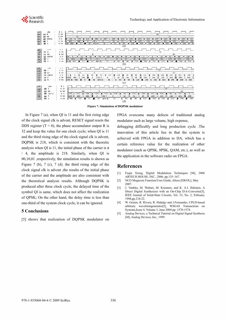
Figure 7. Simulation of DQPSK modulator
In Figure 7 (a), when QI is 11 and the first rising edge
of the clock signal clk is advent, RESET signal resets the
DDS register (T = 0), the phase accumulator output R is
32 and keep the value for one clock cycle; when QI is 11
and the third rising edge of the clock signal clk is advent,
DQPSK is 218, which is consistent with the theoretic
analysis when QI is 11, the initial phase of the carrier is π
/ 4, the amplitude is 218. Similarly, when QI is
00,10,01 ,respectively, the simulation results is shown as
Figure 7 (b), 7 (c), 7 (d). the third rising edge of the
clock signal clk is advent ,the results of the initial phase
of the carrier and the amplitude are also consistent with
the theoretical analysis results. Although DQPSK is
produced after three clock cycle, the delayed time of the
symbol QI is same, which does not affect the realization
of QPSK; On the other hand, the delay time is less than
one-third of the system clock cycle, it can be ignored.
5 Conclusions
[5] shows that realization of DQPSK modulator on
FPGA overcome many defects of traditional analog
modulator such as large volume, high expense,
debugging difficultly and long production cycle .The
innovation of this article lies in that the system is
achieved with FPGA in addition to DA, which has a
certain reference value for the realization of other
modulator (such as QPSK, 8PSK, QAM, etc.), as well as
the application in the software radio on FPGA.
References [1] Fuqin Xiong, Digital Modulation Techniques [M], 2006
ARTECH HOUSE, INC., 2006, pp.135–167. [2] NCO Megacore Function/User Guide, Altera [EB/OL], May
2007. [3] J. Vankka, M. Waltari, M. Kosunen, and K. A.I. Halonen, A
Direct Digital Synthesizer with an On-Chip D/A-Converter[J], IEEE Journal of Solid-State Circuits, Vol. 33, No. 2, February 1998,pp.218-22.
[4] W. Gemin, R. Rivera, R. Hidalgo and J.Fernandez, CPLD-based arbitrary waveformgenerator[J], WSEAS Transactions on Systems,Issue 4, Volume 3, June 2004 pp. 1570-1574.
[5] Analog Devices, a Technical Tutorial on Digital Signal Synthesis [M], Analog Devices, Inc., 1999.
Technology and Application of Electronic Information
978-1-935068-04-4 © 2009 SciRes. 330