
Realization and Measurement of High Frequency Low … · Realization and Measurement of High...
13
© 2014 IJEDR | Volume 2, Issue 2 | ISSN: 2321-9939 IJEDR1402081 International Journal of Engineering Development and Research ( www.ijedr.org) 1783 Realization and Measurement of High Frequency Low Noise Amplifier for Satellite Applications Bhavuk Sharma M.Tech Student Department of Electronics and Communication Manipal University Jaipur, Jaipur, India [email protected] ______________________________________________________________________________________ Abstract - Low Noise Amplifier is an electronic amplifier used to amplify possibly very weak signals. It is usually located very close to the detection device to reduce This active antenna arrangement is frequently used in microwave systems like GPS, because coaxial cable feedline is very lossy at microwave frequencies. An LNA is a key component which is placed at the front – end of the radio receiver circuit. Using an LNA, the effect of noise from subsequent stages of the receive chain is reduced by the gain of the LNA, while the noise of the LNA itself is injected directly into the received signal. Thus, it is necessary for an LNA to boost the desired signal power while adding as little noise and distortion as possible, so that the retrieval of this signal is possible in the later stages in the system. For low noise, the amplifier needs to have a high amplification in its first stage. The four most important parameters in LNA design are: gain, noise figure and impedance matching. The design for LNA is based mainly upon the S-parameters of a transistor. Index Terms- Amplifier, GPS, Coaxial Cable, lossy ________________________________________________________________________________________________________ I. INTRODUCTION This Project entitles “Designing of Low Noise Amplifier” refers to the Satellite Receptor Active Circuit in which reception o f signals take place through the satellite receiving head. In this project we are working in the range of 10.7 GHZ to 12.7GHZ of frequency range. Our main aim is to design and implementation of a Low Noise Amplifier, which provides the gain of 50dB- 60dB in five stages of Low Noise Amplifier. The output of the Satellite Receptor is provided to the TV LNA, radio and through various communication channels. In this project we are using the Advance Designing Software (ADS) of Agilent Technologies for realization purpose. After realization of circuit, measurement of lumped components is done through MICROSCOPE, which measures the thickness of dark and light area and this, we have to design the PCB of the Low Noise Amplifier Circuit. After the completion of the Designing Part we analyze this using NETWORK ANALYSER (Agilent Technology). This project is a part of a large project i.e. Satellite Receiver Active Circuit in which we have to make the LNA part of it. It is a Technical oriented research work, to transform a satellite dish and receiving block Low Noise Amplifier technology into printed circuit type [4]. II. SATELLITE AND ITS WORKING A satellite is an object which has been placed into orbit by human effort. Such objects are called as artificial satellites to distinguish them from natural satellites such as the Moon. Satellites are used for a large number of purposes. Common types include military and civilian Earth observation satellites, communications satellites, navigation satellites, weather satellites, and research satellites. Space stations and human spacecraft in orbit are also satellites. Satellite orbits vary greatly, depending on the purpose of the satellite. They are classified in a number of ways Low Earth Orbit, Polar Orbit, and Geostationary Orbit. Fig.1 Satellite Orbit Satellites are usually semi-independent computer-controlled systems. Satellite subsystems attend many tasks, such as power generation, thermal control, telemetry, attitude control and orbit control. In our project we are using for satellite reception. The
Transcript of Realization and Measurement of High Frequency Low … · Realization and Measurement of High...

© 2014 IJEDR | Volume 2, Issue 2 | ISSN: 2321-9939
IJEDR1402081 International Journal of Engineering Development and Research (www.ijedr.org) 1783
Realization and Measurement of High Frequency
Low Noise Amplifier for Satellite Applications
Bhavuk Sharma
M.Tech Student
Department of Electronics and Communication
Manipal University Jaipur, Jaipur, India [email protected]
______________________________________________________________________________________
Abstract - Low Noise Amplifier is an electronic amplifier used to amplify possibly very weak signals. It is usually located
very close to the detection device to reduce This active antenna arrangement is frequently used in microwave systems like
GPS, because coaxial cable feedline is very lossy at microwave frequencies. An LNA is a key component which is placed at
the front – end of the radio receiver circuit. Using an LNA, the effect of noise from subsequent stages of the receive chain
is reduced by the gain of the LNA, while the noise of the LNA itself is injected directly into the received signal. Thus, it is
necessary for an LNA to boost the desired signal power while adding as little noise and distortion as possible, so that the
retrieval of this signal is possible in the later stages in the system. For low noise, the amplifier needs to have a high
amplification in its first stage. The four most important parameters in LNA design are: gain, noise figure and impedance
matching. The design for LNA is based mainly upon the S-parameters of a transistor.
Index Terms- Amplifier, GPS, Coaxial Cable, lossy
________________________________________________________________________________________________________
I. INTRODUCTION
This Project entitles “Designing of Low Noise Amplifier” refers to the Satellite Receptor Active Circuit in which reception of
signals take place through the satellite receiving head. In this project we are working in the range of 10.7 GHZ to 12.7GHZ of
frequency range. Our main aim is to design and implementation of a Low Noise Amplifier, which provides the gain of 50dB-
60dB in five stages of Low Noise Amplifier. The output of the Satellite Receptor is provided to the TV LNA, radio and through
various communication channels. In this project we are using the Advance Designing Software (ADS) of Agilent Technologies
for realization purpose. After realization of circuit, measurement of lumped components is done through MICROSCOPE, which
measures the thickness of dark and light area and this, we have to design the PCB of the Low Noise Amplifier Circuit. After the
completion of the Designing Part we analyze this using NETWORK ANALYSER (Agilent Technology). This project is a part of
a large project i.e. Satellite Receiver Active Circuit in which we have to make the LNA part of it. It is a Technical oriented
research work, to transform a satellite dish and receiving block Low Noise Amplifier technology into printed circuit type [4].
II. SATELLITE AND ITS WORKING
A satellite is an object which has been placed into orbit by human effort. Such objects are called as artificial satellites to
distinguish them from natural satellites such as the Moon.
Satellites are used for a large number of purposes. Common types include military and civilian Earth observation satellites,
communications satellites, navigation satellites, weather satellites, and research satellites. Space stations and human spacecraft in
orbit are also satellites. Satellite orbits vary greatly, depending on the purpose of the satellite. They are classified in a number of
ways Low Earth Orbit, Polar Orbit, and Geostationary Orbit.
Fig.1 Satellite Orbit
Satellites are usually semi-independent computer-controlled systems. Satellite subsystems attend many tasks, such as power
generation, thermal control, telemetry, attitude control and orbit control. In our project we are using for satellite reception. The
© 2014 IJEDR | Volume 2, Issue 2 | ISSN: 2321-9939
IJEDR1402081 International Journal of Engineering Development and Research (www.ijedr.org) 1784
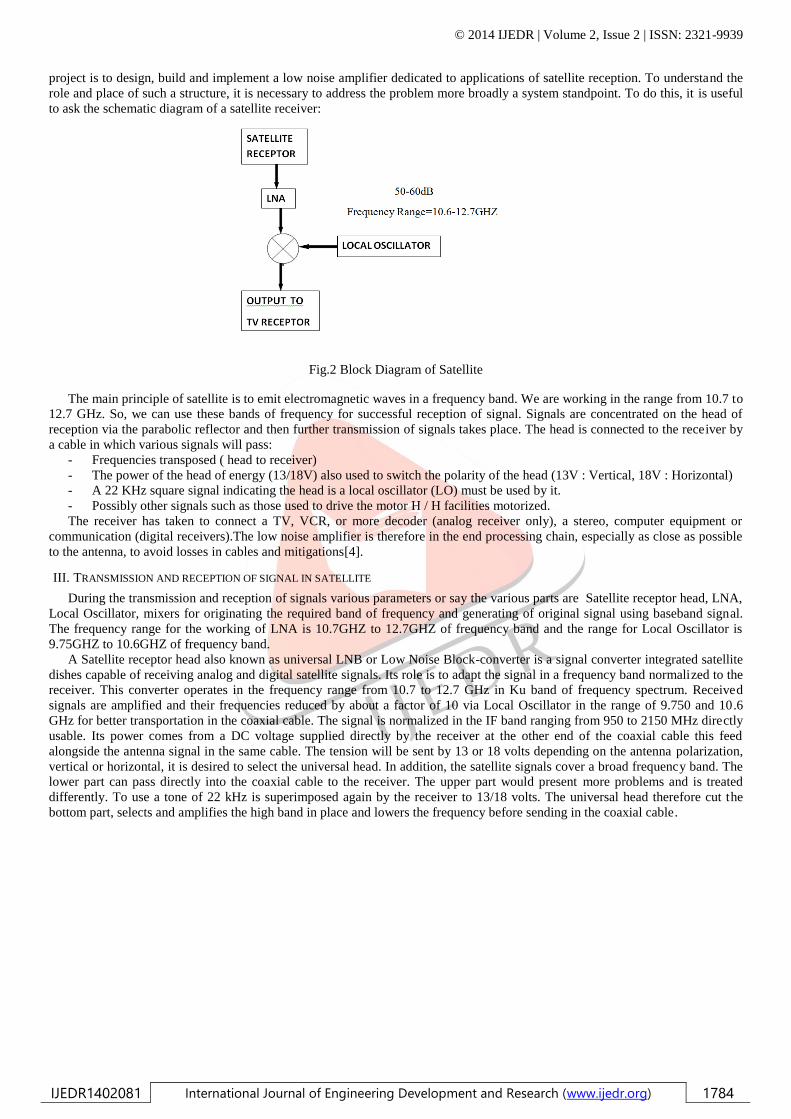
project is to design, build and implement a low noise amplifier dedicated to applications of satellite reception. To understand the
role and place of such a structure, it is necessary to address the problem more broadly a system standpoint. To do this, it is useful
to ask the schematic diagram of a satellite receiver:
Fig.2 Block Diagram of Satellite
The main principle of satellite is to emit electromagnetic waves in a frequency band. We are working in the range from 10.7 to
12.7 GHz. So, we can use these bands of frequency for successful reception of signal. Signals are concentrated on the head of
reception via the parabolic reflector and then further transmission of signals takes place. The head is connected to the receiver by
a cable in which various signals will pass:
- Frequencies transposed ( head to receiver)
- The power of the head of energy (13/18V) also used to switch the polarity of the head (13V : Vertical, 18V : Horizontal)
- A 22 KHz square signal indicating the head is a local oscillator (LO) must be used by it.
- Possibly other signals such as those used to drive the motor H / H facilities motorized.
The receiver has taken to connect a TV, VCR, or more decoder (analog receiver only), a stereo, computer equipment or
communication (digital receivers).The low noise amplifier is therefore in the end processing chain, especially as close as possible
to the antenna, to avoid losses in cables and mitigations[4].
III. TRANSMISSION AND RECEPTION OF SIGNAL IN SATELLITE
During the transmission and reception of signals various parameters or say the various parts are Satellite receptor head, LNA,
Local Oscillator, mixers for originating the required band of frequency and generating of original signal using baseband signal.
The frequency range for the working of LNA is 10.7GHZ to 12.7GHZ of frequency band and the range for Local Oscillator is
9.75GHZ to 10.6GHZ of frequency band.
A Satellite receptor head also known as universal LNB or Low Noise Block-converter is a signal converter integrated satellite
dishes capable of receiving analog and digital satellite signals. Its role is to adapt the signal in a frequency band normalized to the
receiver. This converter operates in the frequency range from 10.7 to 12.7 GHz in Ku band of frequency spectrum. Received
signals are amplified and their frequencies reduced by about a factor of 10 via Local Oscillator in the range of 9.750 and 10.6
GHz for better transportation in the coaxial cable. The signal is normalized in the IF band ranging from 950 to 2150 MHz directly
usable. Its power comes from a DC voltage supplied directly by the receiver at the other end of the coaxial cable this feed
alongside the antenna signal in the same cable. The tension will be sent by 13 or 18 volts depending on the antenna polarization,
vertical or horizontal, it is desired to select the universal head. In addition, the satellite signals cover a broad frequency band. The
lower part can pass directly into the coaxial cable to the receiver. The upper part would present more problems and is treated
differently. To use a tone of 22 kHz is superimposed again by the receiver to 13/18 volts. The universal head therefore cut the
bottom part, selects and amplifies the high band in place and lowers the frequency before sending in the coaxial cable.
© 2014 IJEDR | Volume 2, Issue 2 | ISSN: 2321-9939
IJEDR1402081 International Journal of Engineering Development and Research (www.ijedr.org) 1785
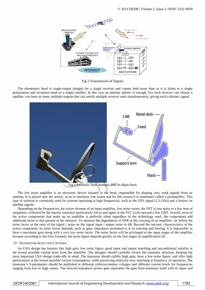
Fig.3 Transmission of Signals
The elementary head is single-output (single) for a single receiver and cannot feed more than as it is limits to a single
polarization and reception band so a single satellite. In this case an antenna splitter is enough. For each receiver can choose a
satellite, you have so many multiple outputs that can satisfy multiple receiver units simultaneously, giving each a distinct signal.
Fig.4 Parabolic Dish Antenna with Its Main Parts
The low noise amplifier is an electronic device situated in the head, responsible for shaping very weak signals from an
antenna. It is placed near the sensor, so as to minimize line losses and for this reason it is sometimes called a preamplifier. This
type of solution is commonly used for systems operating at high frequencies, such as the GPS signal (1.5 GHz) and a fortiori on
satellite signals.
Depending on the frequencies, the active element of an input amplifier, low noise varies; the FET is less noisy to a few tens of
megahertz, followed by the bipolar transistor (particularly SiGe) and again in the FET GaAs beyond a few GHZ. Overall, none of
the active components that make up an amplifier is perfectly silent regardless of the technology used, the components add
additional noise to that present at the entrance. To measure the degradation of SNR at the crossing of an amplifier, we define the
noise factor as the ratio of the signal / noise on the signal input / output noise in dB. Beyond the intrinsic characteristics of the
active component, its noise factor depends, such as gain, impedance presented to it on entering and leaving. It is impossible to
have a maximum gain along with a very low noise factor. The noise factor will be privileged to the input stages of the amplifier
because according to the Friis Formula, the noise figure depends greatly on the first stages of amplification [4].
IV. TRANSISTOR SELECTION CRITERIA
An LNA design has features like high gain, low noise figure, good input and output matching and unconditional stability at
the lowest possible current draw from the amplifier. The designer should carefully review the transistor selection, keeping the
most important LNA design trade-offs in mind. The transistor should exhibit high gain, have a low noise figure, and offer high
performance at the lowest possible current consumption, while preserving relatively easy matching at frequency of operation. The
transistor’s S-parameters should be published at different collector/emitter voltages and different current levels for frequencies
ranging from low to high values. The forward transducer power gain represents the gain from transistor itself with its input and
© 2014 IJEDR | Volume 2, Issue 2 | ISSN: 2321-9939
IJEDR1402081 International Journal of Engineering Development and Research (www.ijedr.org) 1786
output presented with 50Ω impedance. The manufacturer of the transistor at multiple frequencies and different current levels
provides the S21 values. Scattering parameters or S-parameters (the elements of a scattering matrix or S-matrix) describe the
electrical behavior of linear electrical networks when undergoing various steady state stimuli by electrical signals. Different types
of S-Parameters are Z-Parameters, Y-Parameters, ABCD-Parameters, and H-Parameters [1].
V. TWO PORT NETWORK ANALYSIS
Fig.5 Two Port Network
The S-parameter matrix for the 2-port network, serves as the basic building block for generating the higher order matrices for
larger networks. In this case the relationship between the reflected, incident power waves and the S-parameter matrix is given by:
Expanding the matrices into equations gives:
Where,
S11 - is the input port voltage reflection coefficient
S12 - is the reverse voltage gain
S21 - is the forward voltage gain
S22 - is the output port voltage reflection coefficient
Definitions:
1. S11 =b1/a1; for a2 = 0, i.e., input ƒ¡ for output terminated in Zo.
2. S21 =b2/a1; for a2 = 0, i.e., forward transmission ratio with Zo load.
3. S22 =b2a2; for a1 = 0, i.e., output ƒ¡ for input terminated in Zo.
4. S21 =b1a2; for a1 = 0, i.e., reverse transmission ratio with Zo source.
Following are the transistors that meet our requirement of getting the gain of around 50-60dB gain in the frequency range of
10.7-12.7GHZ of frequency band:
1. The NE3210S01 of NEC
2. The EPB018A5 home Excelics
3. The ATF 13736 home Avantek
Transistor appears to be the most advantageous is the NEC: the NE3210S01 that has the lowest NF and gain acceptable for
12 GHz, for its performance and its immediate availability from suppliers, this transistor will be validated to design the low noise
amplifier. Its gain of 13.5 dB, it will be necessary to design several amplification stages in order to reach a final gain of 50dB. To
minimize the possible number of floors, it is possible using a transistor with a gain a little harder while having a noise factor to
correct. Following the first stage designed around NE3210S01. But for reasons of economy, the same transistor will be used in the
overall design of the LNA. It will then make about 5 amplification stages to achieve 50dB of gain [3].
NE3210S01 EPB018A5 ATF 13736
NF 12GHz 0.35 dB Max : 0.45 dB 0.5 dB Max : 0.6 dB 1.8 dB Max : 2.2 dB
Gain at 12GHz 13.5 dB 13 dB 9 dB
Price / Piece 1.12$ 8.90$ Available at Polytech
Table 1 Transistor Configuration

© 2014 IJEDR | Volume 2, Issue 2 | ISSN: 2321-9939
IJEDR1402081 International Journal of Engineering Development and Research (www.ijedr.org) 1787
VI. SUBSTRATE USED
Substrate in electronic wafers and thin film electronics is the physical material upon which a semiconductor device, e.g. a
photovoltaic cell or an integrated circuit, is applied. Micro strip technology is a technology used for producing hybrid
integrated circuits or monolithic hyper frequency. When working in high-frequency transform components located in rows of
printed circuits. This technique has many advantages, including a gain in production cost and saving space on the circuit. The
following diagram shows a sectional view of a micro strip structure. The latter consists of a printed circuit line, height H, width
W and length L, separated from a ground plane by a substrate of relative permittivity epsilon r. This line is made by
photolithographic methods commonly used in the manufacture of printed circuits and so this kind of structure is very easy.
Fig 6 Microstrip Line with Formula
To design a high-frequency micro strip technology, it is necessary to characterize its technology. Their substrates are key
characteristics: the dielectric (εr) constant and dissipation factor (tangent δ). A substrate having a high dielectric constant will
reduce the radiation losses, reducing the value of the wavelength and thus the circuit size. The insertion loss of a circuit is related
to the dielectric substrate. A circuit designed on a substrate having a dissipation factor of the lowest will have the least possible
losses. For further simulations of ADS, the characteristics of substrate will therefore be defined according to a base value:
Epoxy:
Depth of substrate: 1.58 mm
Dielectric constant (εr): 4.4
Dissipation factor tan (δ) = 0.007
Metallization thickness t = 35μm
Roughness R = 0 mm
In general, for the integrated mounting-related phenomena such as the high-frequency discontinuities, only solutions based
on Teflon will be implemented [1].

© 2014 IJEDR | Volume 2, Issue 2 | ISSN: 2321-9939
IJEDR1402081 International Journal of Engineering Development and Research (www.ijedr.org) 1788
Fig 7 Flowchart of LNA Design
VII. LNA DESIGNING USING ADS
The designing of LNA is done by using the ADS (Advanced Design Software) software Agilent Technologies, U.S.A. The
ADS software has comprised of various components i.e. MLEF, MLIN etc that are being used for designing of circuit. ADS
software performs functions like performing Biasing, Polarization, and Optimization. We are working with ADS 2008 version. In
ADS we have to design the LNA having gain of 10.7 dB and we combined the 5 stages of it to achieve the gain of 50-60 dB. We
have got the S-parameter plot of S11, S12, S21 and S22 which satisfies our condition. For satisfying the stability condition the
gain of s11, s12 and s22 less than -10dB of gain and gain of s21 is above 10dB approximately to attain the goal.
Biasing Circuit
Biasing is the method of establishing predetermined voltages or currents to set an appropriate operating point. The operating
point of a device, also known as bias point, quiescent point, Q-point, is the point on the output characteristic that shows the direct
current (DC), collector-emitter voltage (VCE), and the collector current (IC) with no input signal applied. The main purpose of the
bias circuit is to maintain the drain/collector current regardless of any drift in the DC current gain of the Gas FET.
Fig 8 Biasing Circuit
Output graph of the Biasing Circuit is shown below:
Fig 9 Biasing Graph

© 2014 IJEDR | Volume 2, Issue 2 | ISSN: 2321-9939
IJEDR1402081 International Journal of Engineering Development and Research (www.ijedr.org) 1789
Circuit without Polarization
Fig 10 Design without Polarization
Polarization is done to bring the transistor into the desired area of operation. It is done by resistors connected to the circuit
through polarizing filters so as not to interfere as the components in continuous operation at high frequencies. Here, no
polarization filter is connected i.e. no butterfly stub is connected.
DC Biasing and Polarization The DC-biasing is done to set the operating Point of the circuit that is also known as Q-point. Operating Point is required for
the proper operation of the transistor. Polarization is done to bring the transistor into the desired area of operation. These lines
could be quarter-wave high and low impedance in rectangular patches. However for the low impedance element, the width of the
patch is likely to become greater than the length of transverse modes could appear on the edges. To avoid disturbances,
impedance matching is done by connecting a butterfly stub.
Fig 11 Circuit with DC Biasing
Polarization in Biasing
Polarization filter is connected to bring the transistor in the desired working area of the transistor. The design of the filter must
be done to meet the following constraints to the centre frequency.
1. Between the high line impedance and the Butterfly, it should not be mild transmission.
2. Between the high line impedance and the circuit transmission to 0 dB and no reflection.
3. The resistors are connected between the butterfly and the high line impedance.
4. The butterfly has a length of 2.76 mm, a width of 0.5 mm for interfacing with the high line impedance and an angle of
90 °.
Fig 12 Circuit with Polarization

© 2014 IJEDR | Volume 2, Issue 2 | ISSN: 2321-9939
IJEDR1402081 International Journal of Engineering Development and Research (www.ijedr.org) 1790
Fig 13 Polarization Graph
Biasing Used
Basically there are four types 0f FET amplifier biasing. The most common is to have is Voltage Divider Biasing in which
separate DC power supplies for the gate and drain connections, with the gate supply and ground the source. At the base voltage is
divided and the combined output is obtained.
Fig 14 Voltage Divider Biasing
We have used certain equation to compute the following values:
Vgs=Vg-Id*Rs Vp= Pinch Off Voltage
Id=Idss (1-Vgs/Vp) ^2 Id=Drain Current
Vg=Vdd*R2/ (R1+R2) Vg=Gate Voltage
Rs=source Resistance
Given:
Ig=1amp
Vdd=12V
Id=10mA
Vp= -0.45V
The values calculated by using voltage divider biasing are written below:
Rd=470 ohm
Rs=1k parallel with 1k
R1=15k
R2=12k
Impedance Matching
1. Single stub impedance matching - Impedance matching can be achieved by inserting another transmission line (stub)
as shown in the diagram below:

© 2014 IJEDR | Volume 2, Issue 2 | ISSN: 2321-9939
IJEDR1402081 International Journal of Engineering Development and Research (www.ijedr.org) 1791
Fig 15 Single Stub Impedance Matching
There are two design parameters for single stub matching:
a) The location of the stub with reference to the load dstub
b) The length of the stub line Lstub
Any load impedance can be matched to the line by using single stub technique. The drawback of this approach is that if the
load is changed, the location of insertion may have to be moved.
The transmission line realizing the stub is normally terminated by a short or by an open circuit. In many cases it is also
convenient to select the same characteristic impedance used for the main line, although this is not necessary. The choice of open
or shorted stub may depend in practice on a number of factors. A short circuited stub is less prone to leakage of electromagnetic
radiation and is somewhat easier to realize. On the other hand, an open circuited stub may be more practical for certain types of
transmission lines, for example microstrips where one would have to drill the insulating substrate to short circuit the two
conductors of the line [2].
2. Double stub impedance matching - A double stub tuner is a very commonly used impedance-matching network. In
order to make this circuit reconfigurable and achieve a wide load matching capability, either the lengths of both stubs or
the length of one stub and the distance between them needs to be changed significantly.
Fig 16 Double Stub Impedance Matching
Since changing the length between stubs is extremely difficult, for planar and highly integrated of reconfiguring stub length
with variable capacitance. Microwave/Millimeter-wave circuits, reconfigurability can be achieved by fixing the various stub
lengths and terminating each stub with a variable capacitance and each time the capacitance at the end of the stub changes, the
Susceptance at the stub input changes allowing for a different load match [2].
Smith Chart
This method is also used to measure the impedance. By plotting the plot on the graph we can calculate different parameters.
This feature is also available in the ADS software.

© 2014 IJEDR | Volume 2, Issue 2 | ISSN: 2321-9939
IJEDR1402081 International Journal of Engineering Development and Research (www.ijedr.org) 1792
Fig 17 Smith Chart Method
Optimization
It is possible to optimize these results through ads and its optimization tool (tool Optimum and Goal). Optimization is when
you use linear analysis software to vary the values of certain elements within the selected by the user in an attempt to improve the
overall response. Optimization goals are functions that are defined by the user. For example, in designing an amplifier you
probably want a good input and output match, and flat gain.
S11 = 20 dB
S21 = 10dB
S22 = 10 dB
Each goal needs to be assigned a frequency band, and it is evaluated and averaged over that band.
Types of Optimization:
1. Gradient optimization implies that the software is calculating the slope of the error function with respect to each
variable. It does this for each variable separately by making a calculation of the error function, then slightly changing
one variable, calculating the error function again, and using the difference of the two numbers to find the slope.
2. Random optimization is the equivalent of an infinite number of monkeys on an infinite number of computers. It just
takes a guess on what might improve the error function and evaluates the error function with the guess values used for
the variables. Chances are the error function doesn't improve, so the variables are moved to another guess and the error
function is evaluated again.
It is the step by step procedure used to make a design near to is goal by setting the no of iterations. It is the most powerful tool
of linear simulators. It is possible to optimize the lengths and widths of the line to get such a noise figure (NF) of less than 0.5 dB
and nearly constant over the entire band, so that a limited gain for example between 10 and 11.5 dB. The optimizer will be set for
Hybrid Optimization i.e. the total iteration set was 50.

© 2014 IJEDR | Volume 2, Issue 2 | ISSN: 2321-9939
IJEDR1402081 International Journal of Engineering Development and Research (www.ijedr.org) 1793
Fig 18 Optimization Cockpit Window
Fig 19 Optimization Plots of S-Parameter
Layout After getting polarized and optimized graph of LNA Designing, Layout of the circuit is made. The layout of the circuit is
made just by clicking on the menu bar at layout design, and then the designing of the layout is done. Layout shows the physical
appearance of the circuit. After the creation of the layout we go to the next step and the final step i.e. PCB Designing
corresponding to the layout formed.

© 2014 IJEDR | Volume 2, Issue 2 | ISSN: 2321-9939
IJEDR1402081 International Journal of Engineering Development and Research (www.ijedr.org) 1794
Fig 20 Layout Design
Network Analyzer
This is performed to check the gain, stability and overall performance of the circuit. In this, firstly all the setting regarding the
measurement is done and afterwards, we can connect open circuit, shot circuit and matched impedance load to Port 1 and 2 do the
measurement after every connection.
A network analyzer is an instrument that measures the network parameters of electrical networks. Today, network analyzers
commonly measure s–parameters because reflection and transmission of electrical networks are easy to measure at high
frequencies, but there are other network parameter sets such as y-parameters, z-parameters, and h-parameters. Network analyzers
are often used to characterize two-port networks such as amplifiers and filters, but they can be used on networks with an arbitrary
number of ports.
Fig 21 Analysis of Design through Network Analyzer
After doing the analysis through Network Analyzer, we see that we are getting less gain around due to thickness of the line
connected between Butterfly and the transistor. We can do the further analysis of these line connections and the grounding of the
transistor to improve the Gain of the Design. In the design, Grounding means we have to connect the transistor terminal to the 0
volt in place of grounding.
Fig 22 Outlook of Circuit

© 2014 IJEDR | Volume 2, Issue 2 | ISSN: 2321-9939
IJEDR1402081 International Journal of Engineering Development and Research (www.ijedr.org) 1795
VIII. CONCLUSION
A Low Noise Amplifier (LNA) circuit design for frequency of 10.7 GHz to 12.7 GHz presented and circuit simulation which
is done in ADS. LNA has successfully developed with above 10 dB gain and less than 1 dB noise figure at frequency 10.7 GHz to
12.7 GHz. In order to get the gain of 50-60dB, we require a 5-stage amplifier.
In this project, we gain knowledge regarding satellite and transmission of signals. We are using ADS software to design the
LNA circuit using polarization, optimization and layout designing. In this project , we do the analysis of circuit is done by
network analyzer from which till now we are obtaining that some oscillations are there and we are trying to remove all these. The
objectives of the specifications have been met, however, since the noise of the chain is slightly less than 1 dB on the tape, with a
gain between 50 and 60 dB.
REFERENCES
[1] LNA Abstract by Hossein Sahoolizadeh, Alishir Moradi Kordalivand, and Zargham Heidari.
[2] Qian, C., Impedance matching with adjustable segmented transmission line. J. Mag. Reson. 199 (2009), 104-110.
[3] Agilent Technologies: www.agilent.com.
[4] www.wikipedia.com


