“Ready for the Future Technology today”...
83
“Ready for the Future Technology today” 2015
Transcript of “Ready for the Future Technology today”...

“Ready for the Future Technology today”2015
2
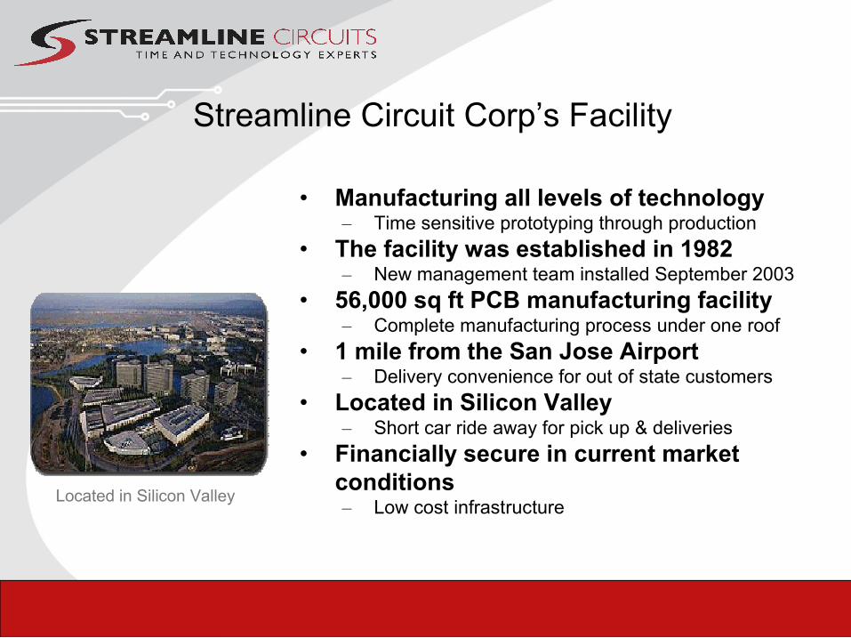
Streamline Circuit Corp’s Facility
• Manufacturing all levels of technology– Time sensitive prototyping through production
• The facility was established in 1982 – New management team installed September 2003
• 56,000 sq ft PCB manufacturing facility– Complete manufacturing process under one roof
• 1 mile from the San Jose Airport – Delivery convenience for out of state customers
• Located in Silicon Valley– Short car ride away for pick up & deliveries
• Financially secure in current market conditions– Low cost infrastructure
Located in Silicon Valley

3
The Team & Their Experience• Chuck Dimick- CEO | Founder
– Over 33 years of experience in PCB manufacturing. Former CEO of Dynamic Details Inc. and founder of the company's predecessor, Dynamic Circuits Inc. (1991)
• Greg Halvorson- President | Founder– Over 31 years of experience in PCB manufacturing. Former VP of Operations of Dynamic Details Inc.
and Dynamic Circuits Inc.
• Tom Doslak-Vice President of Sales & Marketing | Founder– Over 23 years of industry experience. Former Director of Sales for Braztek Intl. and Western Regional
Sales Manager for Dynamic Details Inc.
• Ed Pitney- Operations Manager
– Over with 32 years of PCB manufacturing experience. Ed spent his early career with NTI Inc. as a Director of Manufacturing Operations later purchased by DDI Global Inc.
• Steve Morris – Director of Engineering – Over 27 years of PWB Design & Engineering experiencing. Former VP of Advanced Technology for
Multek (a division of Flextronics) and a key member of the HP PWB Corporate commodity team.
• JR Ramirez- Production Manager | Founder – Over 32 years of experience in the industry. Former Production Manager for both Dynamic Details Inc.
and Dynamic Circuits Inc.
• Lorraine Hook - Director of Quality– Over 43 years of industry experience. Former Director of Quality for many successful companies
including DCI and DDI. She has held dual positions as Corp. Quality Systems Manager.

4
Customer Service Support
• Customer Service (24 hours - 7 days a week)
– Sales, Engineering, Manufacturing and Quality
• Dedicated customer service readily available-our support group’s located onsite in the facility
• Quick response to all requests such as:– Job status
– Delivery pull-in
– Quantity Increases
– Engineering design modification Inside Sales Customer Support
5
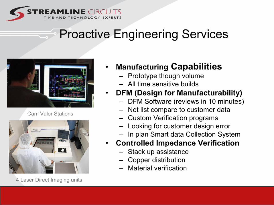
Proactive Engineering Services
• Manufacturing Capabilities– Prototype though volume– All time sensitive builds
• DFM (Design for Manufacturability)– DFM Software (reviews in 10 minutes)– Net list compare to customer data– Custom Verification programs– Looking for customer design error– In plan Smart data Collection System
• Controlled Impedance Verification– Stack up assistance– Copper distribution– Material verification
Cam Valor Stations
4 Laser Direct Imaging units

• DFM Scan & Report
• Stack up assistance
• Copper distribution
• Material verification
• Sub Panel /Array Support
Controlled Impedance Verification
Go to slide 50

7
Quality Reassurance • Net list compare prior to MFG
– Matching Net list to Gerber data
• Front End DRC (design rule check)– Searching for customer design mistakes
• AOI Automated Optical Inspection– Verifying inner & outer layers
• X-Ray Verification– After Lam (Inspecta), After Drilling
• Cross Section Verification– Hole Integrity
• Controlled Impedance Testing– TDR test of panel coupons
• 100% Net List Test On All Product– Eliminator Tester & flying probe
• Coordinate Measurement Machine
– First articles, 100% measurement verification
In house Mil & deliverable Lab
Automated Optical Inspection

8
On Time Delivery Reassurance
• 100% In-house manufacturing from start to finish
– Control delivery & customer flexibility
– In-process quality verification system
– No out sourcing delivery delays
• Employee Training program– Performance evaluation every 6 months
• In-house Chemical Laboratory– Cross Sections
– Chemical analysis
– Mil spec verification
Vacuum Lamination press
8 flying Probe Testers

9
Continuous Improvement Programs
• Working daily on:
– Research and Development
– Pre-Engineering Programs
– Improvement Process Program
– Department Performance Reviews
– Preventative maintenance program
– Employee Training Program
– Planned Capital expense program
Management meetings
7 Laser drills

10
A Full PCB Solution
• Multilayer Rigid / Rigid- Flex / Flex
• 1 to 70 Layers Plus
• 28:1 High Aspect Ratio
• 3.23 Mils Hole to Copper
• Buried / Blind Vias
• 9 Sequential Laminations
• 13+ Stacked Vias
• 1 Mil Trace & Space
• Cavity Constructions
• 6 oz. + Copper Thickness
• Copper Filled Micro Vias
• +/- 5% Controlled Impedance Tol.
• AS9100 Rev. C / ISO 9001
• Mil-Spec 55110 / ITAR
• RoHS & Halogen Free Materials
• IPC 6012 Rigid / 6013 Flex / 6015 MCM / 6016 HDI / 6018 High Frequency
• 3 Mil Mechanical Drills
• 24” x 30” Oversize Panel
• 2 Mil Laser Drill Vias
• Up to 345 Mils Board Thickness
• Via Under Pad (Conductive & Non-Conductive Filled)
• 45+ Materials (Hybrid Constructions)
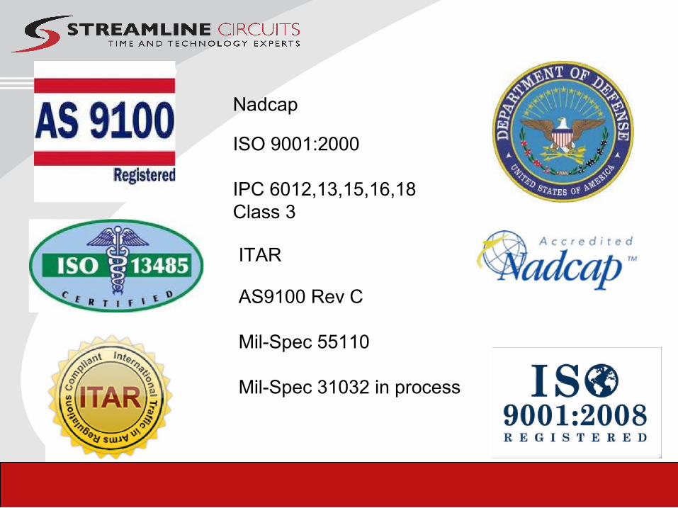
ISO 9001:2000
Mil-Spec 31032 in process
ITAR
AS9100 Rev C
Mil-Spec 55110
IPC 6012,13,15,16,18 Class 3
Nadcap

12
Q-Pulse Total Quality Management
• Quality Assurance Systems• Q-Pulse Quality System
• NCMR’s and Corrective Actions• Audits• Training• Equipment Calibrations
BACK

13
• Use advanced equipment technologies to manufacture today's printed circuit board requirements
• The future in PCB manufacturing is about
technology and automation
• Hire and Train equipment operators
• High percentage engineering personnel and staff
Streamline’s Capital Expenditures
Cuposit & Electroless Line
Laser Direct Imaging
DES Inner Layer Stripline

Design Strategies
Resin Fill off set Vias
Resin fill/stacked Vias
Epoxy fill with copper Vias
All Copper Fill process
15
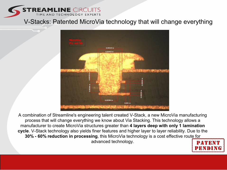
A combination of Streamline's engineering talent created V-Stack, a new MicroVia manufacturing process that will change everything we know about Via Stacking. This technology allows a
manufacturer to create MicroVia structures greater than 4 layers deep with only 1 lamination cycle. V-Stack technology also yields finer features and higher layer to layer reliability. Due to the
30% - 60% reduction in processing, this MicroVia technology is a cost effective route for advanced technology.
V-Stacks: Patented MicroVia technology that will change everything

RIGID-FLEX EXAMPLES
6 Layer Rigid Flex
8 Layer Rigid Flex Micro via
6 Layer Rigid Flex with Cavity
10 Layer Micro via BGA

PCB Equipment Neededfor the Future
Pre ProductionEngineering
LDI ImageProcessing
ElectrolessTechnology
TestProduct Integrity
QualityVerification
Develop EtchStrip
Laser DrillingRegistration
and Micro Via’s
Solder MaskSilkscreen
Test Cases Flex / Rigid-FlexOff-Shore Solution

Flex / Rigid-Flex

RIGID-FLEX EXAMPLES
6 Layer Rigid Flex
8 Layer Rigid Flex Micro via
6 Layer Rigid Flex with Cavity
10 Layer Micro via BGA

Standard Advanced
Layer Count 1L to 6L 8L to 10L
Maximum Panel Size 10”x16” (250x406mm) 10”x35” (250x889mm)
Min. Line/Space (H & ⅓ oz) 0.004" (0.10mm) 0.003" (0.076mm)
Outline Tolerance +/-.004” (0.10mm) +/-.002” (0.05mm) by laser
Stiffener Types PI, FR4+PSA PI, FR4, Steel, Alum
Polyimide Thickness 0.5, 1 mil (12.5, 25um)2, 3, 4 mils (50, 75,
100um)
Base Copper Thickness 0.5, 1 oz (17.5, 35um) ¼ to 2 oz (9 to 70um)
HDI Microvias Yes Yes
Adhesiveless Materials Yes Yes
Flexible Soldermask Yes Yes
White Coverlay Yes Yes
RA Copper Yes Yes
Flex Capabilities
20
Base Material Flex and Rigid Flex
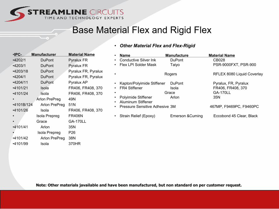
•IPC- Manufacturer Material Name
•4202/1 DuPont Pyralux FR
•4203/1 DuPont Pyralux FR
•4203/18 DuPont Pyralux FR, Pyralux
•4204/1 DuPont Pyralux FR, Pyralux
•4204/11 DuPont Pyralux AP
•4101/21 Isola FR406, FR408, 370
•4101/24 Isola FR406, FR408, 370
• Arlon PrePreg 49N
•4101B/124 Arlon PrePreg 51N
•4101/26 Isola FR406, FR408, 370
• Isola Prepreg FR406N
• Grace GA-170LL
•4101/41 Arlon 35N
• Isola Prepreg P26
•4101/42 Arlon PrePreg 38N
•4101/99 Isola 370HR
• Other Material Flex and Flex-Rigid
• Name Manufacture Material Name• Conductive Silver Ink DuPont CB028• Flex LPI Solder Mask Taiyo PSR-9000FXT, PSR-900
• Rogers RFLEX 8080 Liquid Coverlay
• Kapton/Polyimide Stiffener DuPont Pyralux, FR, Pyralux • FR4 Stiffener Isola FR406, FR408, 370• Grace GA-170LL• Polyimide Stiffener Arlon 35N• Aluminum Stiffener• Pressure Sensitive Adhesive 3M 467MP, F9469PC, F9460PC
• Strain Relief (Epoxy) Emerson &Cuming Eccobond 45 Clear, Black
Note: Other materials javailable and have been manufactured, but non standard on per customer request.

2015
Off-Shore Solution
One Stop PCB Solution
23
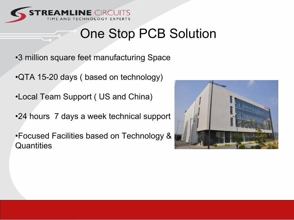
•3 million square feet manufacturing Space
•QTA 15-20 days ( based on technology)
•Local Team Support ( US and China)
•24 hours 7 days a week technical support
•Focused Facilities based on Technology & Quantities

24
Complete Tooling Package
“Build Exact”

25
Integration-Domestic/Offshore
“Build Exact”

Time To Market
“Build Exact”

Intellectual Property
The implementation of strict protection for intellectual property of customers, other than the traditional encryption and decryption.
We provide rigorous authorization and detailed access logs to our employees, in order to control the exchange information.
Move Customers' Logo off and destroy the unusable boards completely.
……

N. AMERICA
S. AMERICA
ASIAEUROPE
AFRICA
OCEANIA
ShanghaiChongqing
Zhuhai
KaiserstraBe, Germany
Plants
Offices
Hangzhou
Headquarter
Page28
Beijing
Texas
California
Oregon Utah
Florida
Shenzhen, Guangdong

Standard Advanced
Maximum Layer Count 36L 40L
Maximum Panel Size 21”x24” (533x610mm) 24”x42” (610x1067mm)
Maximum Finished Thickness 0.126" (3.2mm) 0.256" (6.5mm)
Minimum Finished Thickness 0.006" (0.15mm) 0.004" (0.10mm)
Minimum Core Thickness 0.002” (50um) .0015” (38um)
Trace/Space (H oz) 0.003” .0025”
Maximum Aspect Ratio 14:1 25:1
Minimum Mechanical Drill 0.008" (0.20mm) 0.006" (0.15mm)
Minimum Laser Drill 0.004" (0.10mm) 0.003" (0.076mm)
Min. Soldermask Dam 0.003" (76um) 0.0025" (64um)
Max. Base Copper Thickness 5 oz (75um) 6 oz (210um)
Impedance Control +/- 8% +/- 5%
PCB Capabilities
29

Continual development of new Technologies, Processes, and Materials
•Low Dk/Df, Low CTE, CAF resistant, and Halogen Free FR-4
•High Aspect Ratio Plating (25:1 and 30:1)
•Advanced plating and photo lithography processes
•Advanced tooling systems for registration
•High Technology Radio Frequency (RF) PCB’s
•Metal Backed and Thermal Management PCB’s
•Solid Copper Plating for Through Vias
•Deep Blind Vias and Deep Stacked Microvias
•Embedded Capacitance & Resistance (2015)
•Embedded Heater Circuits (2015)
30
Technology Development
Stacked Microvias
Filled Buried Vias

Manufacturing CapabilitiesSTANDARD ADVANCED
Single-Side Flexible Panel Size
12"x18" 18"x24"
20"x26" 24"x36"
Double-Side Flexible Panel Size 12"x18"
18"x24" and Up
Mulilayer Flexible Panel Size 12"x18"
18"x24" and Up
Layer Count 3 to 12 13+
RIGID FLEX PANEL SIZE 12"x18" 18"x24" and
UpLayer Count 2 to 28 28+
Multiple LaminationCopper Foil Weights Internal/External
1/4 to 2 ounce
Up to 3 ounce
Kapton Polyimide Stiffener .001" to .007".008" and
Up
FR4 Stiffener .003" to .062" .063" and Up
Polyimide Rigid Stiffener .003" to .062" .063" and Up
Lines, spaces & pad diametersInternal Line Width .0035" .001"Internal Spacing .0035" .001"
External Line Width .0035" .001"External Spacing .0035" .001"SMT Pitch .010" .010"
Controlled Impedance 10% 5%
Via hole Finish STANDARD ADVANCED
Laser Micro Vias .004" .002"
Blind/buried Vias .004" .002"
Laser Pads .004" .002"
Minimum Drilled Hole Size .012" .0079"
Drilled Hole to Copper .008" .007"
Castellation Yes Yes
Finish surface
Tin Lead Plating Thickness.0003" to .0005" Less .0005"
Tin Nickel Plating Thickness150 Micro
Inches250 Micro
Inches
Low Stress Nickel100 Micro
Inches250 Micro
Inches
Gold Plating Thickness30 Micro Inches As SpecifiedElectroless Nickel/Immersion
Gold Yes YesImmersion Gold Yes Yes
Immersion Silver Yes Yes
Entek 106A HT Yes Yes
HASL Yes Yes
TOLERANCES
Plated Hole Tolerances (+/-) .002" .001"
Non-Plated Hole Tolerances (+/-) .001" .001"
Fabrication Tolerance (+/-) .005" .003"
Vision Rout (+/-) .003" .002"
Laser Rout (+/-) .002" .001"

CommunicationInfrastructure
IT
CommunicationTerminal Industrial
Equipment
Other Products:Consumer/Office Facilities/
Military/Vehicle/Our products are used inOur products are used in
于
Automobile electronic

Complete
PCB Solution
s
Product Mix
33

Plant ISO9001 TS16949 ISO14001 QC080000 OHSAS18001 GJB9001 TL9000 AS9100 ISO27001
F1 Certified Certified Certified Certified Certified Certified Certified Certified
F2 Certified Certified Certified Certified Certified
F3 Certified Certified Certified Certified Certified Certified
F4 Certified Certified Certified
F5 Certified Certified Certified Certified On-going Certified Certified Certified
F6 Certified Certified Certified Certified Certified Certified Certified
Certifications

Material Type Supplier Product Tg (°C)
High-Tg FR-4
ShengYi S1000-2 175
ITEQ IT180A 175
ISOLA 370HR 175
Mid-Tg FR-4 ShengYi S1000 150
Low-Tg FR-4
ShengYi S1141 140
ITEQ IT-140TC 140
NanYa NY1140 140
Halogen-Free FR-4ShengYi S1155 130
ShengYi S1165 170
High SpeedLow Loss Materials
ISOLA FR408, FR408HR, IS420, IS620, GETEK
Nelco N4000-13, -13EP/SI, N4000-29
Panasonic Megtron4, Megtron6
RogersRO3003, RO3006, RO3010, RO4003C,
RO4350B
Arlon / Taconic PTFE (RF35, TLX, TLY)
Aluminum Yugu YGA Series
Flex Polyimide SY/Taiflex/Panasonic ½, 1 mil, 2 mil PI
Rigid Polyimide Ventec VT901 250
Additional Materials are available.
Materials
35

Revolutionary ZETA® Material•Sunshine is a ZETA® Certified Fabricator
•Glass-free Polyimide Film, 13/25 um [0.5/1 mil]
•Low Dk (3.0-3.4) and low Df (.005-.010)
•Ideal for HDI and High Speed Applications
•High peel strength after multiple lam cycles
•Lead-free compatible and Halogen free
•High dielectric strength
•Eliminates Pad Cratering
36
Copper
B-Stage Epoxy
C-Stage PolyimideCopper
C-Stage Polyimide B-Stage Epoxy
Zeta® Cap Zeta® Bond SE
Zeta® Lam
Graphics provided by Integral Technology
Zeta Certified

37
High Speed Board
•10 Layer HDI
•N4000-13EP
•119x112mm [4.7”x4.4”]
•Thickness 1.6mm [.062”]
•Construction 1+8+1
•Aspect Ratio 10:1
•Via-in-Pad (VIPPO)
•Min L/S .10 mm [.004”]
•Drill/Pad .006”/.016”
•ENIG Finish
•Application: GPS Receiver, Satellite Positioning System
Product Showcase

38
Telecom Linecard
•16 Layer HDI
•370HR
•376x272mm [14.8”x10.7”]
•Thickness 2.21mm [.087”]
•Construction 1+14+1
•Aspect Ratio 11:1
•Via-in-Pad (VIPPO)
•Min L/S .10mm [.004”]
•Drill/Pad .008”/.018”
•Controlled impedance
•ENIG Finish
•Application: Data Server, Communications
Product Showcase

High Layer Count Board•30 Layers
•S1000-2 (Hi-Tg FR4)
•7.0” x 7.0”
•Thickness 3.81mm [.150”]
•25:1 Aspect Ratio with 25 um [1.0 mils] plating required in vias
•Smallest drill .006” on .012” pads
•Via-in-Pad (VIPPO) with maximum dimple 12.5 um [0.5 mils]
•Full body nickel/gold
•Minimum line/space .10 mm [4 mils]
•BGA mounting device positional accuracy requirement
•Fabrication rout tolerance of +/- 0.20 mm [.008”]
39
Product Showcase

ATE Board•34 Layers
•S1000-2 (Hi-Tg FR4)
•368x368mm (14.5”x14.5”)
•Thickness 4.6mm (.180”)
•18:1 Aspect Ratio
•Blind vias from L32-34
•Via-in-Pad (VIPPO)
•Internal Cu: 1 & 2 oz
•Minimum L/S 4 mils
•Drill/Pad .010”/.016”
•Over 20 impedance controlled lines (SE/Diff)
•Countersink holes
•For semiconductor testing
40
Product Showcase

41
Product Showcase
Rigid-Flex
•14 Layer HDI Rigid-Flex•Construction: 14R – 2F – 14R•Min L/S: .10 mm [4 mils]•Thickness: 1.6 mm [.062”]•Application: Medical
•8 Layer Rigid-Flex•Construction: 3R – 2F – 3R•Min L/S: .13 mm [5 mils]•Thickness: 1.0 mm [.040”]•Application: Industrial

42
Product Showcase•RF (Radio Frequency)
•Layer Count: 2L to 10L boards•Mat’l Options: Rogers (4350B, 3010, 4003C), Taconic (RF35, TLX,
TLY)•Hybrid Option: RO4350B + FR4•Finishes: ENIG, Thick Wire Bondable Gold, Flash Gold•Special Process: Selective plating and etching•Applications: Radio Trans-receivers, Antennas, Power Amplifiers

Regular ReliabilityTest
In ProcessQuality Control
TQM Activities(Continuous Improvement)
OutgoingQuality Control
Incoming Quality Control
Panel Control (Traceability)
Quality Assurance
Comprehensive Quality System Structure
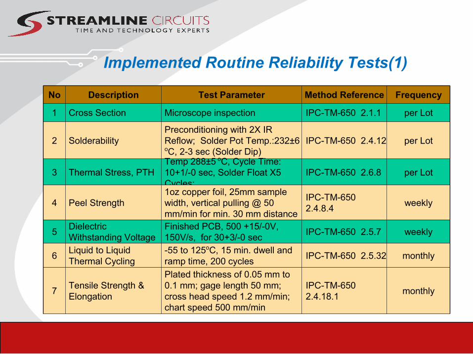
Implemented Routine Reliability Tests(1)
No Description Test Parameter Method Reference Frequency
1 Cross Section Microscope inspection IPC-TM-650 2.1.1 per Lot
2 Solderability Preconditioning with 2X IR Reflow; Solder Pot Temp.:232±6oC, 2-3 sec (Solder Dip)
IPC-TM-650 2.4.12 per Lot
3 Thermal Stress, PTH Temp 288±5 oC, Cycle Time: 10+1/-0 sec, Solder Float X5 Cycles;
IPC-TM-650 2.6.8 per Lot
4 Peel Strength 1oz copper foil, 25mm sample width, vertical pulling @ 50 mm/min for min. 30 mm distance
IPC-TM-650 2.4.8.4
weekly
5Dielectric Withstanding Voltage
Finished PCB, 500 +15/-0V, 150V/s, for 30+3/-0 sec
IPC-TM-650 2.5.7 weekly
6Liquid to Liquid Thermal Cycling
-55 to 125oC, 15 min. dwell and ramp time, 200 cycles
IPC-TM-650 2.5.32 monthly
7Tensile Strength & Elongation
Plated thickness of 0.05 mm to 0.1 mm; gage length 50 mm; cross head speed 1.2 mm/min; chart speed 500 mm/min
IPC-TM-650 2.4.18.1
monthly

Implemented Routine Reliability Tests(2)
No Description Test Parameter Method Reference Frequency
8 CAF Testing 65±2℃, 87+3/-2 %RH, 100V bias, 500 hrs
IPC-TM-650 2.6.3 monthly
9Surface Finish
Thickness
Metal thickness on the pad at four corners and center of the board
IPC-TM-650 2.4.15
per Lot
10Solvent Extracted Contamination (SEC)
75% v/v 2-propanol/water; run time: 30 minutes
IPC-TM-650 2.3.25
per day
11 IR Reflow Simulation Lead: 230±5℃@ 20-30 sec; Lead free: 260±5℃@ 20-30 sec
J-STD-020 per Lot
12Soldermask
Adhesion
3M Brand 600 ½” wide; min. 50 mm in length; perpendicular pulling
Per IPC-TM-650 2.4.1
per Lot
13Interconnect Stress Test (IST))
Ambient temperature to 150 oC, min. 300 cycles
IPC-TM-650 2.6.26
monthly
14 Material Stability
Tg/∆Tg, CTE, T260. Sample is heated at a rate of 5oC/min until all desired transitions have been completed
IPC-TM-650 2.4.24
per day


State of the Art Facilities
Facilities Summary
48
•25 years of PCB fabrication experience in China
•Strong financial backing
•Market/Product focused factories
•State of the art equipment and processes
•QTA/NPI to volume production capabilities
•No constraints on expansion
•Dedicated research and development institute
•Commitment to be the technology leader

Technology Process

50
Pre-Production EngineeringServices
• “In Plan” planning software• Customer Specific Rules Based Automation
• Valor front end CAM (Unlimited Seats)• Industry Standard for front end engineering
• Stack up consultations, Service Offered No Charge $
• Insight Frontline DFM’s, Service Offered No Charge $
• Tech Seminars /Webinars
• Material Science, Latest in Laminates and Pre Preg’s
• R&D, Building the Toughest to Gain the KnowledgeWhen you need it, we will be ready!
BACK
Go to slide 7

High Speed Materials Website Page

Controlled Impedance Verification
•Stack up assistance
•Copper distribution
•Material verification

Hybrid Construction for
low cost (Meg 6 combined with low cost
material for power layer)

54
DFM Report

55
Graphical DFM report
BACK Go to slide 7

56
Imaging System

LDI (Laser Direct Imaging)Orbotech Paragon SM20

58
LDI Imaging Systems
• 100% Laser Direct Imaging (LDI)• Repeatable process, computer controlled• 24/7 consistent imaging regardless of shift• No film means lower tooling costs• No repeating defects
• Consistent trace width• Tighter impedance control (+/- 5 %)• ¼ Mil Accuracy .0008 Min Line/.0005
Space• Layer to layer registration within .0004”• No film growth due to heat expansion BACK
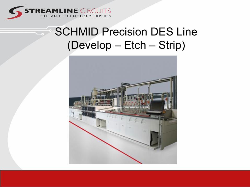
SCHMID Precision DES Line(Develop – Etch – Strip)

60
Inner Layer Develop Etch Strip
• January 2012 State of the art Schmid DES line Installed• Computer controlled for consistent product• Full automation removes human element • 2 Micron variation over panel• 1 mil core capability for substrate, HDI, and Rigid flex• 4,000 Cores per day capacity based on current copper
mix• Tripled capacity upon installation• Positions Streamline for future technologies
BACK

Precision Laser Drilling6 High Speed Laser Drills

62
Laser Drilling
• 6 Laser drills in house (7th has been purchased)• Daily processing 4-N-4 of means experience
• Higher stacks available • .0014” Hole, .004” Pad advances technology window• Aspect Ratio: 3:1• Positional Accuracy for Hole Location +/- .0005”

63
Via formation, Aspect Ratios and Stacked Vias for Increased Densities
BACK

IPS Automatic Electroless Plating Line

65
Electroless Processing
BACK
• Completely Automated Line installed January 2012• Industry leading 28:1 Aspect Ratio: allows for higher
density designs• Bar coded processing removes operator errors• Dwell times established in planning for speed &
efficiency, translating to consistent product • Ultrasonic, knife edge agitation, vibration & thumper• 36 stations, Oversized tanks (24”x 30” Panels)• High volume throughput capability

Everret Charles Flying Probe Testing With the Eliminator

67
Test Capabilities:
• 100% Flying probe testing (8 Systems)• Flexibility, no fixtures, less cost• Allows for testing sub chapters before final book• Everett Charles Eliminator for faster testing• Every board 100% Net List Tested
BACK
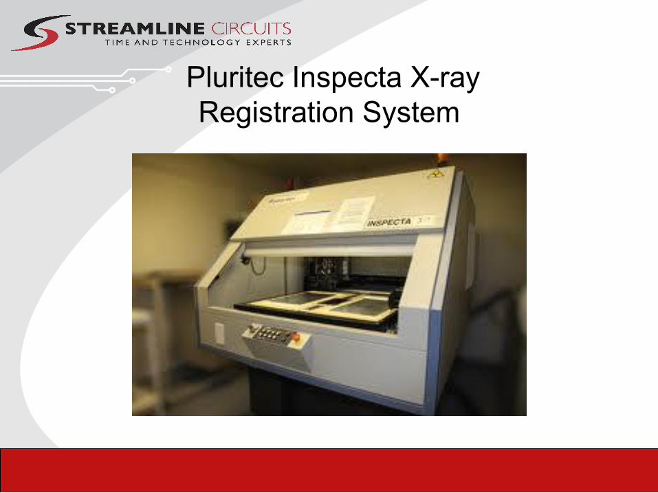
Pluritec Inspecta X-ray Registration System

69
Internal Registration
• In unison with “Xact Software” for scaling
• Internal Registration is one of the key attributes in being successful
• X-Ray allows verification in real time
• X-Sections Verify X-Ray
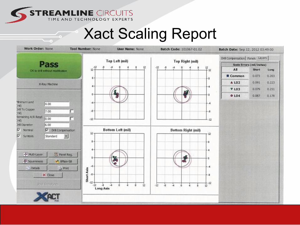
Xact Scaling Report

Non Conductive Filled Via Wrap Per IPC 6012 Class III
Dendrites(Teeth)
SmoothCopper
ElectrolessWrap

72
Copper Fill Laser Vias & Through Hole Solid Copper ViasThermal Via Farms for Thermal Management
BACK

73
• Chip Scale Packaging Requires Streamlines Equipment Sets for
Success-100% LDI
Chip Scale Packaging
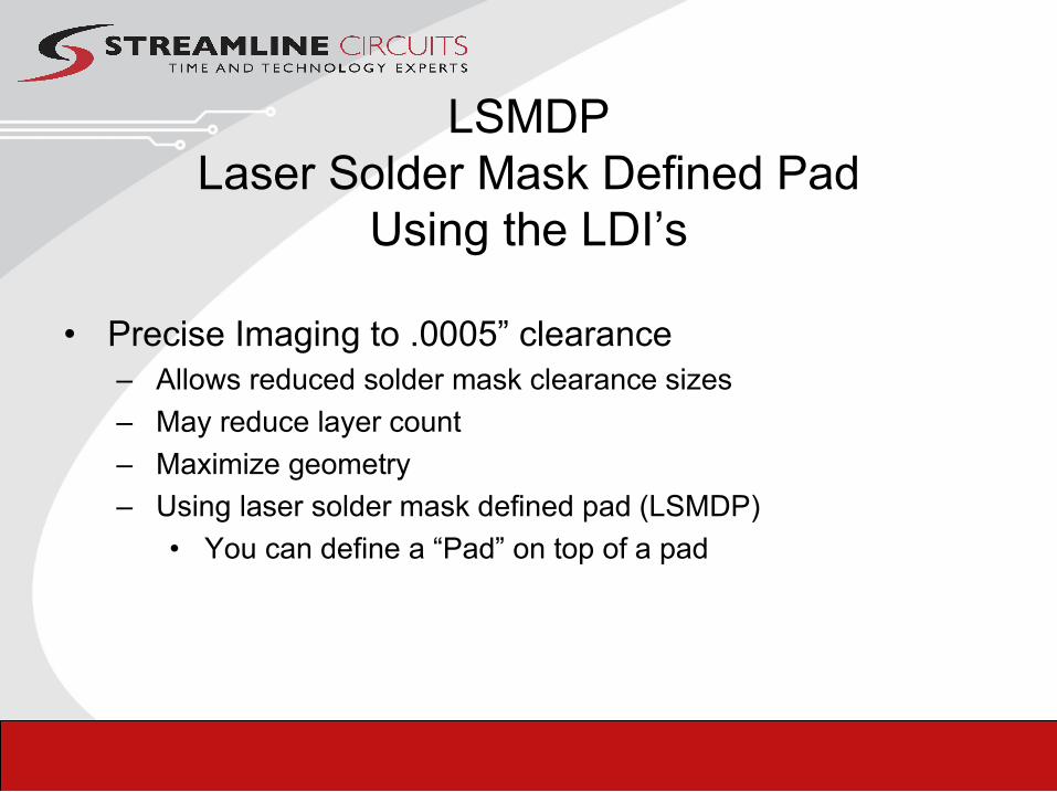
LSMDP Laser Solder Mask Defined Pad
Using the LDI’s
• Precise Imaging to .0005” clearance– Allows reduced solder mask clearance sizes
– May reduce layer count
– Maximize geometry
– Using laser solder mask defined pad (LSMDP)
• You can define a “Pad” on top of a pad

LSMDP (Laser Solder Mask Defined Pad)

Ink Jet SilkscreenOrbotech Sprint-8TM

Ink Jet Silkscreen
“Now Engineers can actually read to debug!”
– Ultra Fine Crisp Lines, Down to 3 mil
– Serialization on the fly, BAR Code & QR codes
– Applied over partially cured mask providing for the mask and legend to be cure simultaneously to reduce cycle time
– Combination inkjet and laser technology
– Dry's the ink as it’s applied
BACK

78
Quality Verification
•Verify Expected Results• 2 X-Section labs on site
• 200 plus sections per day• Wet processing lab onsite• CMM For critical measurement reporting• Two TDR’s for impedance verification• Single ended & diff pairs (Separate testing for
accuracy)• Ionic contamination testing• In process lamination X-ray verification• XRF Gold thickness verification X-Ray

79
Q-Pulse Total Quality Management
• Quality Assurance Systems • Q-Pulse Quality System
• NCMR’s and Corrective Actions• Audits• Training• Equipment Calibrations
• Quality Certifications• IPC Certified Trainers 6012, 13,15,18 • ISO 9001 AS9100C ITAR MIL-P-55110• Mil-P-31032 In Process
BACK

80
Future Investments
• New Schmid outer layer etcher• 2 Orbotech AOI systems with .0005” (1/2 mil) capability• New Electroless Gold line (Enepig)• 2 Additional LDI systems• New Photo plotter for button and silkscreen film• Additional OEM Press•Facility Growth Expansion.
BACK

81
Sample Case #1
Highlights:1/1 Trace Space4 N 4 Stacked Micro Vias.225 mm 1300 Pin BGA1.6 Mil Via – 4 Mil Pad.020 ThickSub Panel Test
Equipment Set:LDI, DESLaser, Inspecta, LDILDI, Inspecta, LDI S/MLDI, Laser, ElectrolessLDI, DES, InspectaFlying Probe

82
Sample Case #2
Speed Test:
• 800ea 10 layers• 2 Lamination cycles• Buried vias, 2-9• Laser Micro Blind 2-3, 8-9• Laser Micro Blind 1-2, 9- 10 with via in pad• 3/3 trace and space• 6.5 PTH to Copper
Delivered in 4 Days

83
Sample Case #3Extremely Thin
• 4 Layer Buried vias 2 -3• 2 Lamination cycles• Laser Micro Blind 1-2, 3-4• Finished thickness .0054• Equipment set
BACK


![1728EX+ : Programming Guide - safe-tech · 02 ... Streamline section Streamline Streamline section Streamline section ... 1728EX+ : Programming Guide Keywords [English] Created Date:](https://static.fdocuments.in/doc/165x107/5b84d6a77f8b9aec488d14a4/1728ex-programming-guide-safe-02-streamline-section-streamline-streamline.jpg)