Reactive Ce3+ on Doped CeO Surface Revealed...
13
1 Highly Enhanced Concentration and Stability of Reactive Ce 3+ on Doped CeO 2 Surface Revealed In operando William C. Chueh 1,2,* , Anthony H. McDaniel 1 , Michael E. Grass 3 , Yong Hao 2 , Naila Jabeen 3,4 , Zhi Liu 3 , Sossina M. Haile 2 , Kevin F. McCarty 1 , Hendrik Bluhm 5 , Farid El Gabaly 1 1 Sandia National Laboratories, Livermore, California 94551, United States 2 Materials Science, California Institute of Technology, Pasadena, California 91125, United States 3 Advanced Light Source, Lawrence Berkley National Laboratory, Berkeley, California 94720 United States 4 Nanosciences & Catalysis Division, National Centre for Physics, Islamabad 44000 Pakistan 5 Chemical Sciences Division, Lawrence Berkley National Laboratory, Berkeley, California 94720 United States Supplementary Information Photolithography Procedure Metal patterns were fabricated by metal liftoff photolithography. Positive photoresist (Shipley 1813) was spin-coated onto YSZ substrates at 2,000 to 3,000 rpm and baked at 115 °C for 150 s. The sample was then aligned with the glass plate mask using a Karl Suss MJB 3 contact aligner and exposed to UV
Transcript of Reactive Ce3+ on Doped CeO Surface Revealed...

1
Highly Enhanced Concentration and Stability of
Reactive Ce3+ on Doped CeO2 Surface Revealed
In operando
William C. Chueh1,2,*, Anthony H. McDaniel1, Michael E. Grass3, Yong Hao2, Naila Jabeen3,4,
Zhi Liu3, Sossina M. Haile2, Kevin F. McCarty1, Hendrik Bluhm5, Farid El Gabaly1
1Sandia National Laboratories, Livermore, California 94551, United States
2Materials Science, California Institute of Technology, Pasadena, California 91125, United States
3Advanced Light Source, Lawrence Berkley National Laboratory, Berkeley, California 94720 United
States
4Nanosciences & Catalysis Division, National Centre for Physics, Islamabad 44000 Pakistan
5Chemical Sciences Division, Lawrence Berkley National Laboratory, Berkeley, California 94720
United States
Supplementary Information
Photolithography Procedure
Metal patterns were fabricated by metal liftoff photolithography. Positive photoresist (Shipley 1813)
was spin-coated onto YSZ substrates at 2,000 to 3,000 rpm and baked at 115 °C for 150 s. The sample
was then aligned with the glass plate mask using a Karl Suss MJB 3 contact aligner and exposed to UV

2
light for 45 to 75 s. Next, the photoresist was developed by immersing the sample in Microposit MF-
319 solution for ~ 30 to 60 s. After rinsing by deionized water and drying, the sample was cleaned using
an oxygen plasma to remove residual organics and then transferred to a DC magnetron sputtering
system (AJA International) where Pt (99.99 % purity) was deposited in 3 milltorr Ar. The growth rate
was approximately 10 nm min-1 and the total thickness approximately 200 nm. Metal liftoff was
performed by immersing the samples in acetone at room temperature. The above procedure was
repeated for the other side of the substrate to make a symmetric cell.
Additional Physical Characterization
Epitaxy of the film was confirmed by X-ray diffraction (Figure S1). In-plane diffraction pattern shows
the expected four-fold rotation symmetry of the (220) peak when the (200) oriented sample was titled by
45 ° and rotated about the sample normal axis. Furthermore, the SDC thin film shows excellent registry
alignment with the YSZ substrate. Out-of-plane diffraction pattern only contained the (200) family
peaks, again confirming the eptixay. The rocking curve yielded a full-width half-max of 0.30°. A cross-
sectional scanning electron micrograph of a typical sample, Figure S2, shows the two morphological
regions of SDC: columnar-type growth over Pt and epitaxial growth over YSZ.
-180 0 180
YSZ (220)
SDC(220)
/
Inte
nsity
/ ar
b. u
nit
20 40 60 80 100 120
SD
C (
200)
SD
C (
600)
SD
C (
400)
YS
Z (
400)
2 /
Inte
nsity
/ ar
b. u
nit
YS
Z (
200)
15 16 17 18
SDC (200)
Inte
nsity
/ ar
b. u
nit
/
FWMH = 0.30
Figure S1. (a) In-plane, (b) out-of-plane, and (c) rocking curve X-ray diffraction pattern for SDC(100)
without the burried Pt electrical contacts. Cu kα X-ray source (45 kV, 40 mA) was used.
B CA

3
SDC on YSZ SDC on Pt
YSZ
Pt
1 µm1 µm
Figure S2. Cross-sectional scanning electron micrograph of SDC(100) with buried electrical contacts.
(a) (b)
Figure S3. In-situ low-energy electron diffraction patterns for SDC collected at (a) 1.8 × 10⁻⁶ Torr O2 ,
740 °C (oxidizing condition) and (b) 1.0 × 10⁻⁷ Torr H2, 600 °C (reducing condition) using 19 eV
electrons. The patterns are consistent with a first-order diffraction from SDC(100). These diffuse
features are due to secondary electrons.
Electrochemical Impedance Spectroscopy
A one-dimensional Poisson-Nernst-Planck transport model has been proposed and validated for the
thin film solid-state electrochemical cell utilized here.1,2 This transport model, discussed briefly below,
is used to determine the bulk oxidation state, 3+[Ce ]bulk , from the impedance response. We consider
mixed oxygen vacancy and electron conducting thin films grown on both sides of a pure ion-conducting
4
substrate. Because of the aspect ratio of the thin films used here, the rate of oxygen incorporation and
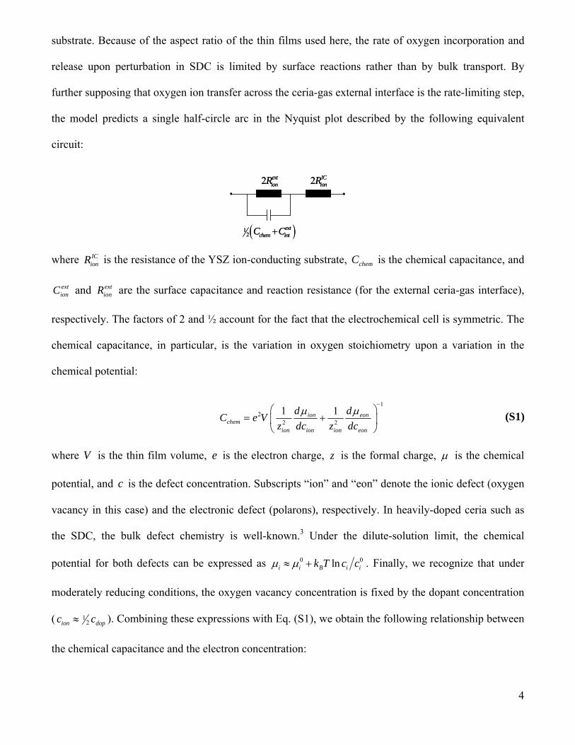
release upon perturbation in SDC is limited by surface reactions rather than by bulk transport. By
further supposing that oxygen ion transfer across the ceria-gas external interface is the rate-limiting step,
the model predicts a single half-circle arc in the Nyquist plot described by the following equivalent
circuit:
12
extchem intC C
2 extionR 2 IC
ionR
12
extchem intC C
2 extionR 2 IC
ionR
where ICionR is the resistance of the YSZ ion-conducting substrate, chemC is the chemical capacitance, and
extionC and ext
ionR are the surface capacitance and reaction resistance (for the external ceria-gas interface),
respectively. The factors of 2 and ½ account for the fact that the electrochemical cell is symmetric. The
chemical capacitance, in particular, is the variation in oxygen stoichiometry upon a variation in the
chemical potential:
1
22 2
1 1ion eonchem
ion ion ion eon
d dC e V
z dc z dc
(S1)
where V is the thin film volume, e is the electron charge, z is the formal charge, is the chemical
potential, and c is the defect concentration. Subscripts “ion” and “eon” denote the ionic defect (oxygen
vacancy in this case) and the electronic defect (polarons), respectively. In heavily-doped ceria such as
the SDC, the bulk defect chemistry is well-known.3 Under the dilute-solution limit, the chemical
potential for both defects can be expressed as 0 0lni i B i ik T c c . Finally, we recognize that under
moderately reducing conditions, the oxygen vacancy concentration is fixed by the dopant concentration
( 12ion dopc c ). Combining these expressions with Eq. (S1), we obtain the following relationship between
the chemical capacitance and the electron concentration:

5
12 1
2eonchem B dop
e Vc
C k T c
(S2)
In a wide band gap semiconductor such as ceria ( gE 6 eV), electron-hole pair formation due to
thermal excitation is negligible. Therefore, the polaron concentration can be directly correlated to the
bulk oxidation state, with 3+ 0[Ce ] /bulk eon eonc c , where 0eonc is the concentration of all Ce ions. This
approach of correlating the thin film capacitance to the bulk oxidation state can be easily extended to
non-dilute solutions by modifying the functional form of the chemical potential.
A typical impedance spectrum is shown in Figure S4 in the Nyquist form. A small high-frequency
feature is visible, which is not predicted by the impedance model. It has been shown elsewhere that this
feature is related to the electronic current constriction near the perimeter of the buried metal current
collector.4 We account for this effect by adding an additional resistor-capacitor network in series with
equivalent circuit. Furthermore, we also observe that the main arc in the Nyquist plot takes a slightly
depressed semi-circular shape, rather than a perfect half-circle. This non-ideal behavior can attributed to
the dispersion in the characteristic frequency, for example, due to variation in the film thickness. To
account for such non-ideality, we replace the ideal capacitor in the parallel resistor-capacitor network
with a constant-phase element, with the impedance given as 1m
CPEZ j Y
, where 1j and
is the angular frequency. It can be shown that the equivalent capacitance of the constant-phase element
is 1 1 1m m
eqC Y R , where R is the resistance. The modified equivalent circuit is fitted to the impedance
spectrum, Figure S4. The surface capacitance ( extionC ) was reported elsewhere1 to be approximately
4 mF cm-2 and independent of temperature and pressure. Using Eq. (S2), the bulk Ce3+ fraction is
calculated from the fitted chemical capacitance.
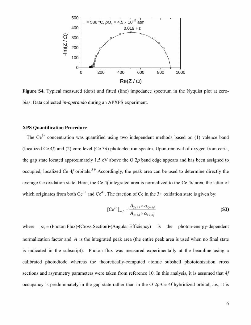
6
0 200 400 600 800 10000
100
200
300
400
500
-Im
(Z /
)
Re(Z / )
0.019 Hz
T = 586 C, pO2 = 4.5 10-25 atm
Figure S4. Typical measured (dots) and fitted (line) impedance spectrum in the Nyquist plot at zero-
bias. Data collected in-operando during an APXPS experiment.
XPS Quantification Procedure
The Ce3+ concentration was quantified using two independent methods based on (1) valence band
(localized Ce 4f) and (2) core level (Ce 3d) photoelectron spectra. Upon removal of oxygen from ceria,
the gap state located approximately 1.5 eV above the O 2p band edge appears and has been assigned to
occupied, localized Ce 4f orbitals.5-9 Accordingly, the peak area can be used to determine directly the
average Ce oxidation state. Here, the Ce 4f integrated area is normalized to the Ce 4d area, the latter of
which originates from both Ce3+ and Ce4+. The fraction of Ce in the 3+ oxidation state is given by:
Ce 4 Ce 43+
Ce 4 Ce 4
[Ce ] f dsurf
d f
A
A
(S3)
where (Photon Flux) (Cross Section) (Angular Efficiency)i is the photon-energy-dependent
normalization factor and A is the integrated peak area (the entire peak area is used when no final state
is indicated in the subscript). Photon flux was measured experimentally at the beamline using a
calibrated photodiode whereas the theoretically-computed atomic subshell photoionization cross
sections and asymmetry parameters were taken from reference 10. In this analysis, it is assumed that 4f
occupancy is predominately in the gap state rather than in the O 2p-Ce 4f hybridized orbital, i.e., it is
7
fully localized. It was verified experimentally that the gas-phase X-ray attenuation was not a strong
function of h between 270 eV and 390 eV.
Turning to the core-level analysis, the Ce3+ concentration was determined using a linear combination
of two Ce 3d spectra:
'''
'''
Ce 3 ,3+ Ce 3
Ce 3Ce 3 ,
[Ce ] 1oxd
d u dsurf oxd
dd u
A A
A A (S4)
where the superscript “oxd” indicates the reference spectra taken under a sufficiently oxidizing
condition such that 3+[Ce ]surf can be approximated as zero, and '''u denotes the highest binding energy
peak in the Ce 3d envelope. Here, a photoelectron spectrum collected at 465 °C and 7 × 10⁻⁶ Torr O2 is
taken as the oxidized reference spectrum (Figure 3b). Under this condition, an occupied Ce 4f state in
the band gap is completely absent and confirms the oxidized nature of ceria surface. This approach
assumes that the mixed valent Ce 3d spectra is a linear combination of the fully oxidized and fully
reduced spectra, and that the '''Ce 3 ,d u peak area scales linearly with 4+[Ce ]surf . These assumptions are
generally valid for moderate values of 3+[Ce ]surf .11
Finally, the dopant (Sm) concentration was determined using:
Sm 3 Sm 3
Ce 4 Ce 4 Sm 3 Sm 3
/[Sm]
/ /d d
surfd d d d
A
A A
(S5)
Because of the proximity of the Sm 4d and Ce 4d binding energies, the same photon energy was used
( h = 390 eV) and the electron attenuation length was assumed to be the same. The quantification result
is shown in Figure S5. A linear background was used for Ce 3d, Ce 4d, and Sm 4d photoemission,
whereas a Shirley background was used for the valence band spectra.
To examine the consistency of the two quantification methods, 3+[Ce ]surf determined from Ce 3d and
Ce 4f analysis are plotted against each other in Figure S6. Overall, good linearity is obtained, with the
slope close to 1.
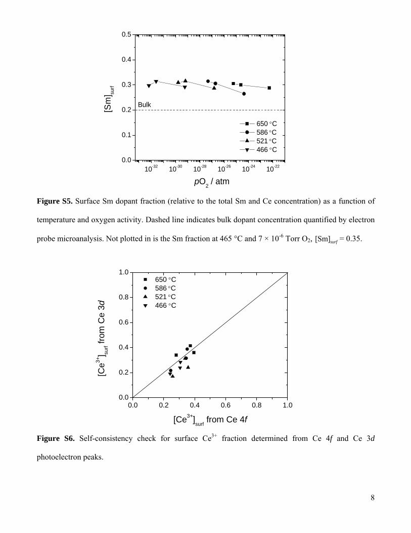
8
10-32 10-30 10-28 10-26 10-24 10-220.0
0.1
0.2
0.3
0.4
0.5
Bulk
650 C 586C 521C 466 C
[S
m] su
rf
pO2 / atm
Figure S5. Surface Sm dopant fraction (relative to the total Sm and Ce concentration) as a function of
temperature and oxygen activity. Dashed line indicates bulk dopant concentration quantified by electron
probe microanalysis. Not plotted in is the Sm fraction at 465 °C and 7 × 10⁻⁶ Torr O2, [Sm]surf = 0.35.
0.0 0.2 0.4 0.6 0.8 1.00.0
0.2
0.4
0.6
0.8
1.0 650 C 586C 521C 466 C
[Ce3+
] surf fr
om C
e 3d
[Ce3+]surf
from Ce 4f
Figure S6. Self-consistency check for surface Ce3+ fraction determined from Ce 4f and Ce 3d
photoelectron peaks.

9
Effective Attenuation Length
Calculation
The effective attenuation length (EAL) was calculated using the NIST Standard Reference Database
8212 based on the TPP-2M predictive equation for the electron inelastic mean free paths. The parameters
used for the calculation are summarized in Table S1. Because the composition changes near the sample
surface, it is important to examine how this affects the EALs. Specifically, the EALs were computed for
two compositions: Sm0.2Ce0.8O1.9 (bulk) and Sm0.5Ce0.5O. The variation in EALs was less than 6 % in
the kinetic energy range examined. Therefore, the scattering properties are taken to be uniform within
the sample.
Table S1. Parameters used for calculating the effective attenuation length of Ce 4f photoelectrons.
*The six 5p electrons in Ce are included in the valance electron count as they contribute strongly to the
energy-loss spectrum.13 ** Two values of band gap are reported in literature: the gap between valence
band maximum and the localized Ce 4f (~ 3 eV) state, and the gap between the valence band maximum
and the conduction band minimum (~ 6 eV). It is not immediately clear which value is more suitable in
calculating the inelastic mean free path, though the calculated EALs differ by less than 3 %.
Composition Sm0.2Ce0.8O1.9
Density 7.2 g cm-3
Number of valence electron* 20.4
Asymmetry Parameter10 0.770 ( h = 270 eV)
Band gap** 6 eV
X-ray incidence angle (with respect to surface normal)
15 ° (Beamline 11.0.2)
75 ° (Beamline 9.3.2)
Electron emission angle (with respect to surface normal)
-40 ° (Beamline 11.0.2)
0 ° (Beamline 9.3.2)

10
Correction
With the EALs calculated, it is possible to correct for the finite XPS penetration depth and estimate
the composition on the topmost surface. The simplest approach is to approximate the sample as a bilayer
structure, consisting of an overlayer (of thickness t ) with an unknown composition and a substrate with
a known composition. By integrating the mass attenuation equation (with intensity originating from
depth z given by 0 exp ( cos )I I z EAL , where is the electron emission angle with respect to
the surface normal), we obtain the following expression for the corrected composition of the surface
overlayer:
3+ 3+3+ [Ce ] [Ce ] exp ( cos )
[Ce ]1 exp ( cos )
surf bulkol
t EAL
t EAL
(S6)
To carry out this correction, the overlayer thickness needs to be specified. While this quantity is not
available experimentally, a lower bound can be readily estimated. By recognizing that 3+[Ce ]ol cannot
exceed one and assuming that the layer thickness does not change with experimental conditions, one
obtains:
3+ 3+[Ce ] [Ce ] exp ( cos )1
1 exp ( cos )surf bulk t EAL
t EAL
(S7)
Because the EAL depends on the overlayer thickness, we solve the equation iteratively. Dopant
concentration in the overlayer is estimated in the same manner.
Using Eq. (S7), the upper-bound limit for the 3+[Ce ] at the outermost surface is, for all temperature and
pressure conditions, a factor of 2.5 - 2.6 greater than shown in Figure 2, with the lowest and highest
values being 0.64 and 1.0, respectively. The variation of oxidation state with oxygen activity (i.e., the
slope in Figure 2) and the chemical potentials are essentially unchanged. Assuming the same
segregation length scale for Ce3+ and Sm, the upper-bound value for [Sm]surf in the outermost surface
11
ranges from 0.33 to 0.43, again, slightly exceeding the directly computed values. The lower bound
thickness (~ 2 Å) of the outermost layer corresponds to approximately half the unit cell thickness in
ceria (ao = 5.4 Å) and suggests that approximately two atomic planes in the (100) orientation are
disrupted by the surface termination.
Surface OH Concentrations
Surface OH concentration was qualitatively assessed by comparing O 1s photoelectron spectra
collected under humidified and dry conditions. We first measured the O1s spectra under H2-H2O
atmospheres at 650 °C. Subsequently, we evacuated the chamber to <10-7 Torr at ~460 °C, backfilled
with 7 x 10⁻⁶ Torr O2, and collected an O 1s spectrum after equilibration. As evident in Figure S7, the
spectra taken under dry and wet environments are qualitatively similar to each other and do not show a
significant change in the high binding energy shoulder (OH is expected at ~2.5 eV above the lattice
oxygen peak14). Based on temperature-programmed desorption results, OH on CeO2 begins to
decompose at ~230 °C.14 Given our much higher sample temperature, we expect that any surface OH
species would have desorbed from the surface at 460 °C under < 10-7 Torr. This data suggests that
surface OH coverage is very low at 650 °C, particularly when compared to that of the Ce3+
concentration. We did not attempt to analyze O1s spectra further due to the lack of reference spectra
under high temperature, ambient pressure conditions. We speculate that the high binding energy
shoulder could be due to surface lattice oxygen, surface oxygen vacancy defects, or impurities.

12
536 534 532 530 528
Inte
nsity
/ ar
b
Binding Energy / eV
10 mTorr H2O, 10 mTorr H
2, 650 C
300 mTorr H2O, 10 mTorr H
2, 650 C
7 x 10⁻⁶ Torr O2, 466 C
Figure S7: O 1s spectra at various conditions at 650 °C. For clarity, the binding energy of the lattice
oxygen peak is aligned to that in the spectrum taken under oxidizing condition (slight energy shifts are
observed due change in the electron chemical potential in ceria upon interaction with the gas). Intensity
is also normalized to the lattice oxygen peak. Measured at a photon energy of 800 eV.

13
REFERENCES
(1) Chueh, W. C., California Institute of Technology, 2011.
(2) Jamnik, J.; Maier, J. Phys. Chem. Chem. Phys. 2001, 3, 1668.
(3) Kobayashi, T.; Wang, S.; Dokiya, M.; Tagawa, H.; Hashimoto, T. Solid State Ionics 1999, 126, 349.
(4) Brown, E., California Institute of Technology, 2011.
(5) Henderson, M. A.; Perkins, C. L.; Engelhard, M. H.; Thevuthasan, S.; Peden, C. H. F. Surf. Sci. 2003, 526, 1.
(6) Mullins, D. R.; Overbury, S. H.; Huntley, D. R. Surf. Sci. 1998, 409, 307.
(7) Ganduglia-Pirovano, M. V.; Hofmann, A.; Sauer, J. Surf. Sci. Rep. 2007, 62, 219.
(8) Pfau, A.; D., S. K. Surf. Sci. 1994, 321, 71.
(9) Mullins, D. R.; Radulovic, P. V.; Overbury, S. H. Surf. Sci. 1999, 429, 186.
(10) Yeh, J. J.; Lindau, I. Atomic Data and Nuclear Data Tables 1895, 32, 1.
(11) Shyu, J. Z.; Otto, K.; Watkins, W. L. H.; Graham, G. W.; Belitz, R. K.; Gandhi, H. S. J. Catal. 1988, 114, 23.
(12) Powell, C. J.; Jablonski, A. NIST Electron Effective-Attenuation-Length Database Version 1.3, SRD 82; National Institute of Standards and Technology: Gaithersburg, MD, 2011.
(13) Tanuma, S.; Powell, C. J.; Penn, D. R. Surf. Interface Anal. 2003, 35, 268.
(14) Kundakovic, L.; Mullins, D. R.; Overbury, S. H. Surf. Sci. 2000, 457, 51.


![SDC-12/SDC-15 · 2018-01-14 · Introduction 6 SDC-12/SDC-151080pD-ILA3D Front Projector2013 User’s Manual AdditionalOptionalAccessories Replacementlamps: •FormodelsSDC-12andSDC-15[2013productionandbeyond]orderlampWC-LPU230](https://static.fdocuments.in/doc/165x107/5f30eb9530d2254a2869f490/sdc-12sdc-15-2018-01-14-introduction-6-sdc-12sdc-151080pd-ila3d-front-projector2013.jpg)