Ray Edgerton Workshop on EELS Canadian …kavanagh/StrucAnallMat/EELS-wrkshop-MSC'07.pdfRay Edgerton...
48
Ray Edgerton Workshop on EELS Canadian Microscopical Society Meeting, U. of Alberta, Edmonton, June 14, 2007
Transcript of Ray Edgerton Workshop on EELS Canadian …kavanagh/StrucAnallMat/EELS-wrkshop-MSC'07.pdfRay Edgerton...

Ray Edgerton Workshop on EELS
Canadian Microscopical Society Meeting, U. of Alberta,
Edmonton, June 14, 2007

Particle picture of scattering
elastic inner-shell inelastic outer-shell inelastic

Energy-loss spectrum (log-intensity) of YBCO courtesy of D.H. Shin, Cornell University

energy-band diagram
valence or conduction
band
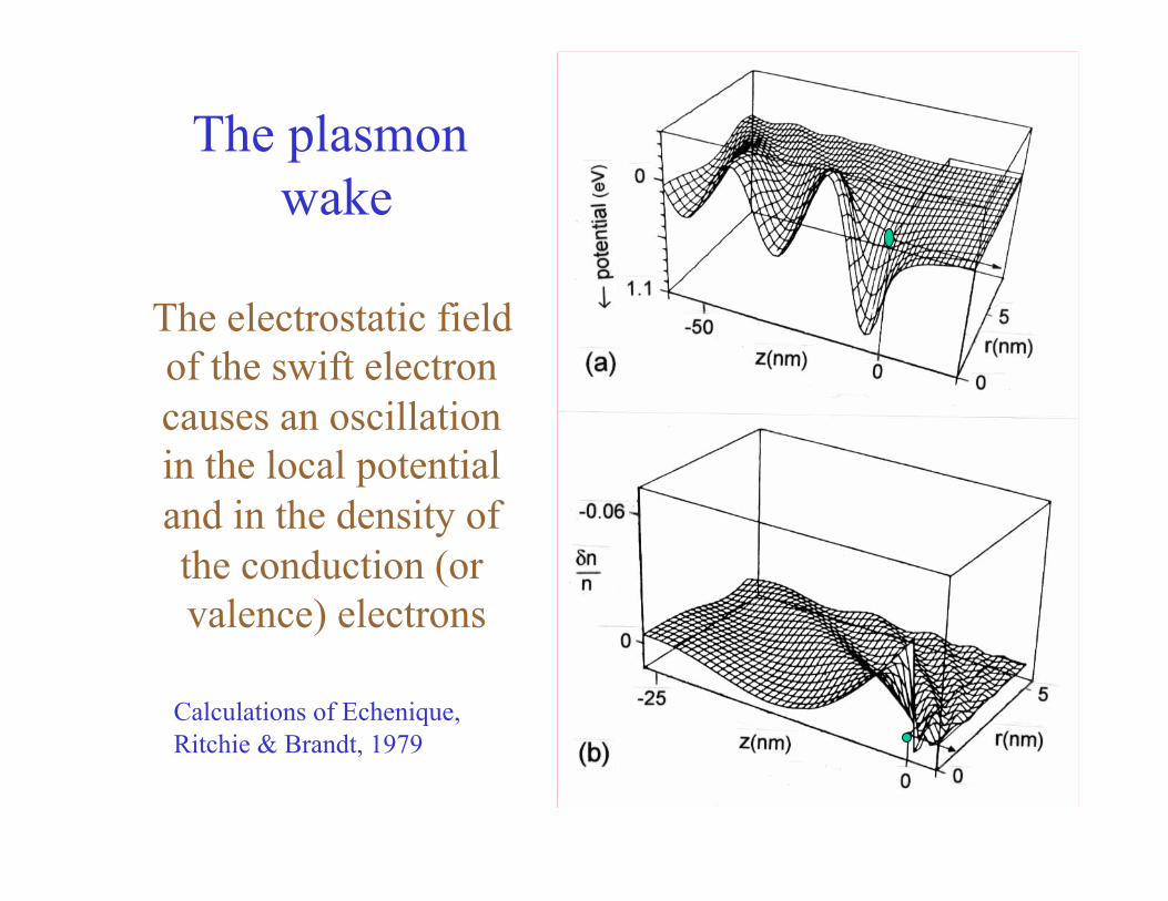
The plasmon wake
The electrostatic field of the swift electron causes an oscillation in the local potential and in the density of the conduction (or valence) electrons
Calculations of Echenique, Ritchie & Brandt, 1979

Plasmon energies of the elements
solid circles: Ep = (h/2π)(ne2/ε0m) with m = m0 and n = density of “outer-shell” electrons
crosses: experimental values (Colliex, 1984)

Plural (multiple) scattering
silicon
zero-loss
first-plasmon

Plural scattering: Pn = (1/n!) mn exp(-m) where m = t/λ t = specimen thickness and λ = inelastic mean free path

Comparison of the elastic and
inelastic angular
distributions
scattering angle (mrad)
0 10 20 30
normalized intensity 0
1
Z = 6 , E0=200keV
scattering angle (mrad)
0 10 20 30
normalized intensity 0
1elastic (amorphous)elastic (polycrystal)inelastic (30 eV)inelastic (300 eV)
30eV 300eV

EELS instrumentation
• Below the TEM: • Serial EELS (e.g. Gatan 607) • Parallel EELS (e.g. Gatan 666) • Gatan Enfina • Gatan Imaging Filter • In-column: • Prism-mirror (Leo) • Omega Filter (Leo, JEOL)

A magnetic prism bends, disperses and focuses an electron beam
e v B = F = mv2/R
R = (m/e)(v/B) R

Parallel-mode recording (Gatan Enfina system)

Gatan Image Filter (GIF)

Leo-922 energy-filtering TEM
omega filter

Omega-filter in-column spectrometer
energy-selecting slit
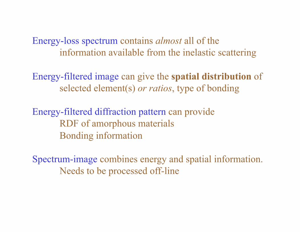
Energy-loss spectrum contains almost all of the information available from the inelastic scattering
Energy-filtered image can give the spatial distribution of selected element(s) or ratios, type of bonding
Energy-filtered diffraction pattern can provide RDF of amorphous materials Bonding information
Spectrum-image combines energy and spatial information. Needs to be processed off-line

Ways of recording energy-loss data in the TEM

field-emissionsource
TEMcondenser
lenses
TEMimaginglenses
EELS detector
thinspecimen
angle-limiting
aperture
TEMviewingscreen
TEMcondenser
lenses
imaginglenses and
prism system
probe -forminglenses
focusinglenses
(optional)
prism prism
electronsource
annularelectrondetector
(a) (b) (c)
scancoils
Spectrometer beneath TEM
In-column filter
STEM system

TEM screen spectrometerobject plane
EELS spatialresolution isdetermined by:
EELS angularrange β isdetermined by:
advantages anddisadvantages
Image Diff-Pat SEA or SAA orelectron probe
OBJ-AP convenientlens aberration
Diff-Pat Image electron probeor SAA
SEA orOBJ-AP
high intensitygood en. resoln.proj alignment
OA
SAA
specimen
spectrometer
SEA
e-probe
screen
Two basic operating modes for a spectrometer located below the TEM screen

Applications of EELS
1. Measurement of local thickness
2. Elemental analysis (quantitative)
3. Element or thickness mapping
4. Fine-structure analysis
5. Study of radiation damage

Measurement of specimen thickness
t/λ = loge(It/I0)
1. Measure relative thickness t/λ 2. Take λ(nm) ~ E0(keV) 3. λ(Z, E0 and β) from parameterized formula 4. λ(Z, E0 and β) from calibration specimen or from tables (for common materials)

The fitted curve is MFP given by λ = 106 F (E0/Em) ln(2β E0 /Em)
(λ in nm, β in mrad, E0 in keV Em in eV)
F = 1.04 (E0 = 200keV)
Em = 7.6Z0.36
(Malis et al., JEMT 1988)

Absolute thickness
measured by Kramers-Kronig
sum rule horizontal line is calibration value
Yang and Egerton, 1995 (Micron 26, 1)

EELS elemental analysis
Competitive with XEDS for light elements (standardless, no need for absorption corrections)
Background subtraction very important (characteristic features are edges, not peaks)
Cross sections available for most edges
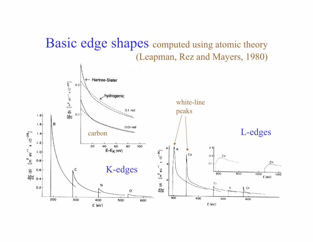
Basic edge shapes computed using atomic theory (Leapman, Rez and Mayers, 1980)
white-line peaks
K-edges
L-edges carbon

Pre-edge background subtraction
1. Blind extrapolation (e.g. AE-r )
2. Guided extrapolation
3. MLS spectral fitting

Elemental quantification
Absolute: NA = [IA(β,Δ) / Ilowloss(β,Δ)] / σA(β,Δ)
Relative: NA/NB = [ IA(β,Δ)/IB(β,Δ) ] [σB(β,Δ)/σA(β,Δ)]

Smart-fit algorithms (Afit, Bfit, Cfit) Egerton and Malac, Ultramicroscopy 92 (2002) 47

Fitting to spectral standards (Leapman et al., Ultramicroscopy, 1993)
First-difference spectra
Endoplasmic reticulum
Fitted calibration spectrum
Ca/C ~ (1.1±0.1) x10-4 for 336 sec acquisition and area < 1 µm2

Core-loss cross sections Hydrogenic model (SIGMAK, SIGMAL programs)
Hartree-Slater model (Leapman et al. 1980, Rez 1989)
Experimental (Malis & Titchmarsh 1986, Hofer 1987)
Parameterized (SIGPAR, recent Gatan software)

Energy-filtered imaging
EFTEM or STEM mode ? (acquisition time etc.)
Spectrum-image recording ? (easiest in STEM)
Thickness mapping based on t/λ = ln(It/I0)
Elemental mapping (background subtraction by 2- or 3-window method) Gives areal density = concentration × thickness
Jump-ratio map reduces thickness dependence Element-ratio map eliminates thickness dependence

200kV GIF elemental maps of Co particles
showing an oxide skin
Disko et al., Proc. M&M 2001, p.1090)
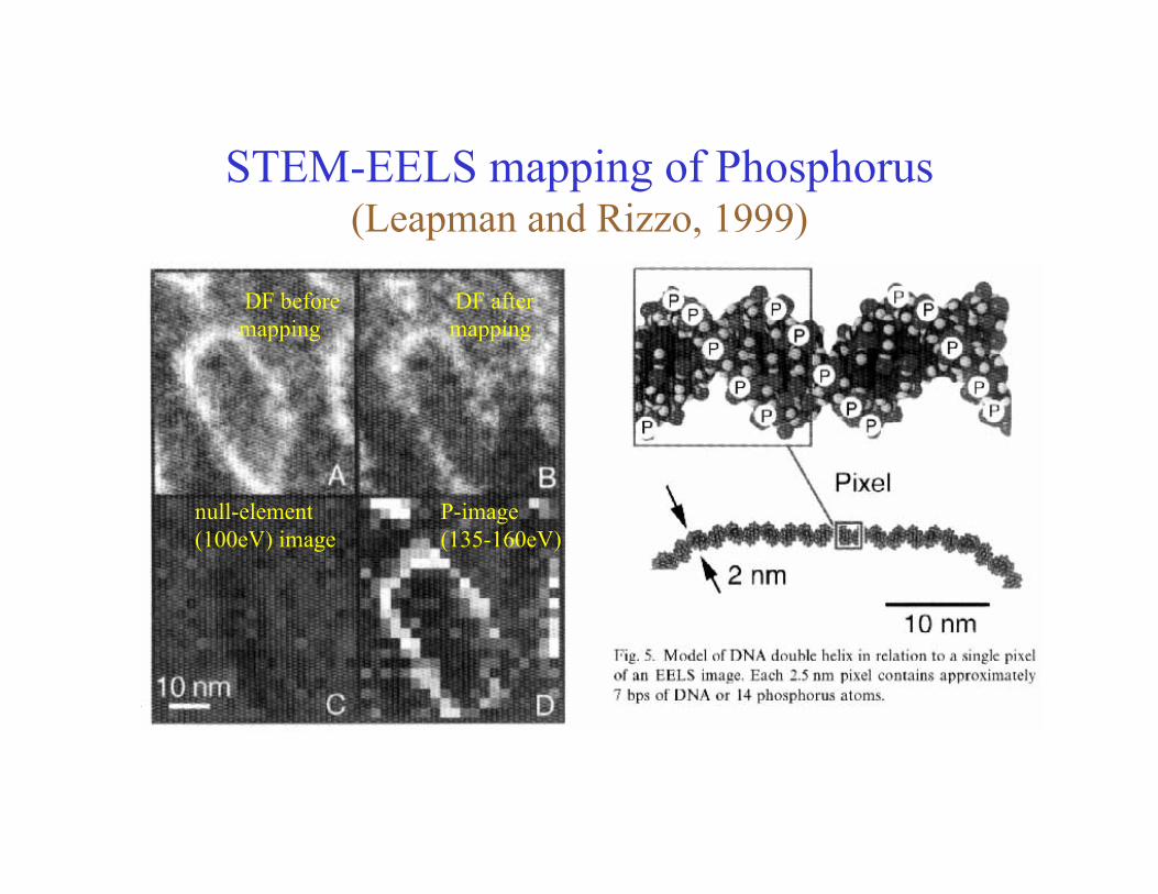
STEM-EELS mapping of Phosphorus (Leapman and Rizzo, 1999)
DF before mapping
DF after mapping
null-element (100eV) image
P-image (135-160eV)

ADF imaging & EELS of a CoS2-Si interface (Browning, Chisholm & Pennycook, 1993)

EELS fine structure
Low-loss region or ionization edges
Energy resolution is important (monochromator or field-emission source helps, energy width increases with emission current) Detector PSF can be significant (work at largest dispersion to minimize “tails’)
Often a “fingerprint” technique, although fine structure calculations can help in interpretation.
q-dependence can be helpful in distinguishing collective/single-particle and bulk/surface peaks
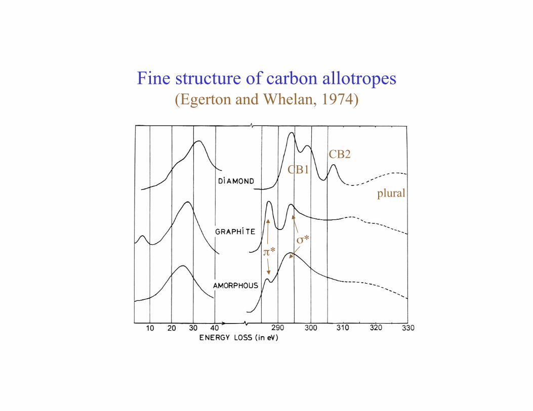
Fine structure of carbon allotropes (Egerton and Whelan, 1974)
CB1 CB2
plural
π* σ*

K-edge spectra of diamond and grain from the
Allende meteorite
(Blake et al., Nature 332, 1988, 611)
π*

Low-loss and K-edge spectra of fullerite thin films (Kuzuo et al., Phys. Rev. B49, 1994, 5054)

Core-loss fine structure reflects local DOS of empty conduction-band states (initial state = core level, more or less sharp in energy)
Low-loss fine structure is more complicated since it reflects JDOS between valence and conduction band but usually superimposed on (bulk and surface) plasmon peaks, collective modes which can be quite complicated in the case of small particles & nanostructures.

Detector PSF
Due to light spreading in the scintillator, the response to a narrow electron beam shows “tails” that extend over 10 or more channels. Their extent in eV can be reduced by using high spectrum dispersion (< 0.1 eV/channel)

Use of a monochromator (0.15eV resolution) helps in revealing the bandgap in ZnO. Also, displacing the collection aperture (or tilting the illumination) away from q = 0 helps.
From Wang et al., Micron 38 (2007) 346.
Bandgap detection and measurement using EELS

q-dependence of fine structure can be useful in identifying the nature of fine-structure peaks. For example, a surface-plasmon peak has a relatively narrow angular width and disappears when the collection aperture is shifted slightly off-axis.
From Wang et al., Micron 38 (2007) 346.
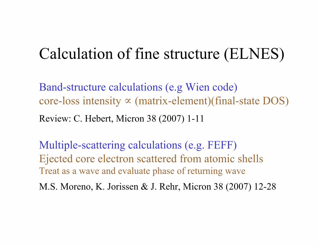
Calculation of fine structure (ELNES)
Band-structure calculations (e.g Wien code) core-loss intensity ∝ (matrix-element)(final-state DOS) Review: C. Hebert, Micron 38 (2007) 1-11
Multiple-scattering calculations (e.g. FEFF) Ejected core electron scattered from atomic shells Treat as a wave and evaluate phase of returning wave M.S. Moreno, K. Jorissen & J. Rehr, Micron 38 (2007) 12-28
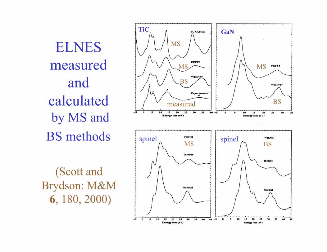
ELNES measured
and calculated by MS and
BS methods
(Scott and Brydson: M&M
6, 180, 2000)
MS
MS MS
MS
BS
BS measured
TiC GaN
spinel spinel BS

White lines in Ce-based
catalysts
Krause, Proc EMSA (1991) Crozier & McCartney, 1996

Oxidation state of Cr in a bacterium
(Daulton et al,
M&M 7, 479, 2001)

Use of EELS in the study of radiation damage
Mass loss can be studied by low-loss or core-loss spectroscopy Change in elemental composition by core-loss spectroscopy Change in chemical bonding by fine-structure analysis (e.g disappearance of 6eV peak can indicate loss of double bonds)

Dose (C/cm2)
0.0 0.5 1.0 1.5 2.0
6eV peak A
rea/Initial Area
0.2
0.3
0.4
0.5
0.6
0.70.80.9
0.1
1
Radiation damage: reduction of the 6eV peak in coronene
from Li & Egerton, Ultramicroscopy 101 (2004) 161.