Rapid Production of Transparent Structured Substrates for ...epubs.surrey.ac.uk/755157/1/Mills Nova...
47
Published in: New nanotechnology research. Ed: Reece JP. 199-234. Nova Science Pub Inc. 2006 1 Rapid Production of Transparent Micro/Nanostructured Polymer Substrates for Biomedical Surface Interaction Studies Christopher A. Mills, Elisabeth Engel, Elena Martinez, Mateu Pla-Roca, Miriam Funes, Francois Bessueille, Abdelhamid Errachid, Josep Planell and Josep Samitier Laboratory of Nanobioengineering (CREBEC), Barcelona Science Park, Josep Samitier 1-5, 08028 Barcelona, Spain. Tel: +34 93 403 48 80 Fax: +34 93 403 71 81 http://www.pcb.ub.es E-mail: [email protected] ABSTRACT The increase in the number of investigations into biomedical interactions with structured substrates has produced a necessity for transparent, micro- and nanostructured surfaces. To facilitate research, it must be possible to use these structured surfaces in conjunction with established culturing and imaging apparatus available within a biomedical laboratory. Such surfaces can be produced using a rapid fabrication technique where freestanding, transparent, structured polymeric substrates are produced for use in cell-surface interaction experiments. The production method is based on a nanoimprint lithography (NIL) technique using silicon based moulds to emboss structure into the surface of biologically compatible thermoplastic polymers. The moulds are fabricated via deep reactive ion or focused ion beam lithographies. The polymers can then be sized to fit in existing cell culture plates, or can be employed with reusable silicon-based culture plates. Unstructured polymers fabricated using this technique have transparencies rivalling that of glass, and although the transparency of the micro- and nanostructured films is reduced slightly, they are still sufficiently transparent to be used with conventional transmission microscopes. Cells cultured on the micro/nanostructures can therefore be viewed both from above and through the substrate, allowing cell-structure interactions, which would normally be hidden by the bulk of the cell, to be viewed. The optical transparency of the structured polymers also allows them to be used in
Transcript of Rapid Production of Transparent Structured Substrates for ...epubs.surrey.ac.uk/755157/1/Mills Nova...

Published in: New nanotechnology research. Ed: Reece JP. 199-234. Nova Science Pub Inc. 2006
1
Rapid Production of Transparent Micro/Nanostructured Polymer Substrates for
Biomedical Surface Interaction Studies
Christopher A. Mills, Elisabeth Engel, Elena Martinez, Mateu Pla-Roca, Miriam Funes,
Francois Bessueille, Abdelhamid Errachid, Josep Planell and Josep Samitier
Laboratory of Nanobioengineering (CREBEC), Barcelona Science Park,
Josep Samitier 1-5, 08028 Barcelona, Spain.
Tel: +34 93 403 48 80 Fax: +34 93 403 71 81
http://www.pcb.ub.es
E-mail: [email protected]
ABSTRACT
The increase in the number of investigations into biomedical interactions with
structured substrates has produced a necessity for transparent, micro- and
nanostructured surfaces. To facilitate research, it must be possible to use these
structured surfaces in conjunction with established culturing and imaging apparatus
available within a biomedical laboratory. Such surfaces can be produced using a rapid
fabrication technique where freestanding, transparent, structured polymeric substrates
are produced for use in cell-surface interaction experiments. The production method is
based on a nanoimprint lithography (NIL) technique using silicon based moulds to
emboss structure into the surface of biologically compatible thermoplastic polymers.
The moulds are fabricated via deep reactive ion or focused ion beam lithographies. The
polymers can then be sized to fit in existing cell culture plates, or can be employed with
reusable silicon-based culture plates.
Unstructured polymers fabricated using this technique have transparencies
rivalling that of glass, and although the transparency of the micro- and nanostructured
films is reduced slightly, they are still sufficiently transparent to be used with
conventional transmission microscopes. Cells cultured on the micro/nanostructures can
therefore be viewed both from above and through the substrate, allowing cell-structure
interactions, which would normally be hidden by the bulk of the cell, to be viewed. The
optical transparency of the structured polymers also allows them to be used in

Published in: New nanotechnology research. Ed: Reece JP. 199-234. Nova Science Pub Inc. 2006
2
fluorescent techniques. The possibility of chemically functionalising the polymer
surfaces further increases the useful applications of these substrates.
KEYWORDS: Nanostructure, microstructure, polymer, embossing, surface
functionalisation, biomedical applications.

Published in: New nanotechnology research. Ed: Reece JP. 199-234. Nova Science Pub Inc. 2006
3
CONTENTS
1. Introduction
2. Surface micro/nanostructuring techniques
2.1 Topological surface micro/nanostructuring
2.1.1 Mask-based lithography micro/nanofabrication techniques
2.1.2 Direct-write and other nanofabrication techniques
2.2 Polymer substrates
2.2.1 Embossing micro/nanofabrication techniques
2.2.2 2-D versus 3-D polymer surfaces
2.3 Topological micro/nanostructure characterisation
2.4 Summary
3. Surface chemical functionalisation techniques
3.1 Chemical functionalisation
3.1.1 Direct functionalisation
3.1.2 Indirect functionalisation
3.1.3 Surface wettability – an example of one effect of indirect chemical
modification
3.2 Polymer surface functionalisation
3.2.1 Gas discharge techniques
3.2.2 Chemical modification of polymer surfaces
3.2.3 Grafting
3.3 Functionalised layer characterisation
3.4 Protein immobilisation - an example of an application for chemically
functionalised surfaces
3.5 Summary
4. Biomedical applications
4.1 Imaging
4.2 Adhesion, proliferation and differentiation
4.3 Cellular structuring
4.4 Tissue formation
5. Rapid replication technique
5.1 Silicon mould fabrication
5.2 Polymer embossing
5.3 Polymer replica characterisation

Published in: New nanotechnology research. Ed: Reece JP. 199-234. Nova Science Pub Inc. 2006
4
5.4 Sterilisation
5.5 Chemical functionalisation of polymer surfaces
5.6 Biomedial applications of patterned polymer surfaces
6. Conclusion
Acknowledgement
References

Published in: New nanotechnology research. Ed: Reece JP. 199-234. Nova Science Pub Inc. 2006
5
1. INTRODUCTION
It is natural for scientists and engineers to mimic nature in trying to develop
applications relevant to both biological and medical fields. This is especially true for
applications utilising structured and patterned surfaces. Although methods for the
structuring of surfaces, at dimensions comparable to those commonly found in nature
(i.e. at size ranges from micrometres downwards), has been available for some time, it is
only lately that the technology has been available to synthetically fabricate such
morphological and chemical surface patterns with controllable geometries.
It has long been known that the morphology of surfaces plays an important role
in biology. Biological systems that may be affected range from the production of 3-
dimensional (3-D) tissues, to the alignment of individual cells on 2-dimensional (2-D)
structures. The effects of topological structuring do not, however, simply end at the
positioning and orientation of cells. Various studies are now discovering that the
interaction of a cell with a structured surface can also affect the adhesion properties of
the cell to the surface [1, 2, 3] and even the function of stem cells [4].
As with many techniques, the need to produce physical structures at very small
dimensions can be traced back to the electronics industry. Moore‟s Law [5] describes
the need for an increasing number of transistors on a single integrated circuit. This need
has consequently led to improved lithography methods for transistor production.
Fortunately, the appearance of these new lithographic techniques has had a knock-on
effect in opening other application areas which benefit all branches of the physical
sciences and society in general; for example, as the basis for micro-electro-mechanical
systems (MEMS), microfluidics, and microarray technology.
The production of micro- and nanoscale chemical patterns has been another
challenge which, through careful development, has lead to a number of breakthroughs.
Surface patterning techniques, such as microcontact printing [6] and dip pen lithography
[7], can be used to produce chemical patterns with dimensions down to sub-micrometer
levels over large areas [8]. Such techniques can also be used for the deposition and
alignment of more than one chemical species. In areas such as microarray patterning,
this has lead to the development of on-chip sequencing and diagnostic systems [9, 10].
Improvements in lithography and chemical patterning, along with a greater
understanding of material and surface properties, have allowed experts within the
biomedical field to collaborate in producing surfaces useful for a range of applications.
One example of a group of increasingly useful materials is biodegradable polymers.

Published in: New nanotechnology research. Ed: Reece JP. 199-234. Nova Science Pub Inc. 2006
6
These can be used in polymeric surgical implants (such as screws) which are degraded
by the body over time, and hence do not require a second operation for removal [11].
Knowledge of the surface properties of the polymer has helped to ensure that the
implants heal the affected tissue without being rejected by the host body.
Here we present a method for the rapid production of micro/nanostructured
polymeric surfaces for in-vitro biomedical cell-surface interactions. We describe
examples of micro and nanostructuring methods which can produce a regular
topological structure at micron and sub-micron dimensions, and explain why polymer
surfaces formed in this way have advantages over techniques using inorganic materials,
especially when it comes to fabrication, diversity of chemical and physical properties
and biocompatibility. We then describe methods of surface chemical functionalisation,
concentrating on polymer surface modification, which allows tuning of the surface
chemical and physical properties to be undertaken. Finally, we present some results
showing how micro/nanostructured polymeric surfaces can be prepared, cheaply and
quickly, using compression moulding techniques, and how they can be used for in-vitro
cell-surface interactions in biomedical applications.
2. SURFACE MICRO/NANOSTRUCTURING TECHNIQUES
2.1 Topological surface micro/nanostructuring
There are a number of methods for the structuring of surfaces on micron and
sub-micron levels. Traditionally, before the advent of more advanced fabrication
technologies, these relied on mechanical or chemical treatments of the surface, that
imparted structuring, but in a manner that was not well controlled. For example,
mechanical polishing or chemical etching of metals and inorganic materials (e.g. glass
and silicon) can produce surfaces with regular structuring at micron scales, but at
smaller dimensions the patterning is much more random [12].
2.1.1 Mask-based lithography micro/nanofabrication techniques
The advent of mask-based photolithography has increased the control of surface
patterning at micron scales. These days, the best photolighographic/chemical etching
methods can achieve sub-micron resolutions [13]. This advance in particular has led to
the establishment of microengineering disciplines for microelectromechanical systems
(MEMS) and microfluidics, miniaturised total analytical systems (-TAS) and
miniaturised laboratory devices (lab-on-a-chip) [14].

Published in: New nanotechnology research. Ed: Reece JP. 199-234. Nova Science Pub Inc. 2006
7
Other developments, such as the invention of the electron beam lithography
(EBL) technique, and the later development of deep ultraviolet (UV) and x-ray
lithography techniques, have further expanded the field of mask-based lithography.
However, the latter techniques suffer from problems with source and mask production,
respectively [15]. Therefore, EBL is the method of choice for structure production using
polymer resists (such as poly(methyl methacrylate) (PMMA)) with a resolution down to
10 nm [15].
Post-lithographic pattern transfer processes have also been improved. Reactive
ion etching (RIE), has allowed the fabrication of structures with aspect ratios superior to
those developed using wet etching techniques, with increasingly vertical side-walls and
much smoother surfaces [16].
However, one problem that dogs mask-based lithography techniques is the need
to use a mask and the use of potentially harmful photoresist chemicals that must be
disposed of carefully. The mask must have a lateral feature resolution suitable for the
technique, a non-trivial task when sub-100 nm features are required. Wet etching
compounds the problem of chemical safety/disposal, as it uses other, inherently
corrosive, chemicals for the etching of the inorganic substrate. Further, a combination of
photolithography and etching requires two steps, which increases the possibility of
errors and is time consuming (although there have been recent developments in mask-
less lithography [17, 18]).
2.1.2 Direct-write and other nanofabrication techniques
Lately, direct-write techniques, such as focussed ion beam (FIB) milling [19] or
laser milling [20] have been developed. In both techniques material is directly removed
from the surface of the substrate. The techniques use focused, computer-controlled,
high-energy beams: ions for FIB and light for laser milling respectively. In such
methods, the need for a mask and a variety of chemicals is negated. However, at this
time, the resolution of these direct-write techniques is limited by the spot-size of the
beam that can be focussed on the substrate surface. In laser milling the spot size is
limited to the micron range [20], whereas for FIB milling it can be as low as 30 nm
[21].
Other direct-write nanofabrication techniques suitable for the production of
surface structures include scanning probe techniques, epitaxy and molecular self-
assembly [15]. The scanning probe techniques (e.g. nanomanipulation, dip pen etc.)
Published in: New nanotechnology research. Ed: Reece JP. 199-234. Nova Science Pub Inc. 2006
8
have the advantage of being highly controllable, but the disadvantage that they are serial
and difficult to scale up for large-scale production. Epitaxial methods are limited to
inorganic substrate modification, but do have the advantage that they can be used to
pattern large areas.
Similarly, self-assembly techniques can be used to pattern large areas, but they
are hampered by the presence of impurities and, sometimes, the need to use complex
chemical production methods. However, a problem for the examination of biological
specimen stems from a lack of methods for the preparation of well defined organic
surfaces. Surface assembled monolayers (SAMs), particularly those formed by the
adsorption of long-chain alkanethiols, are well suited for studying interactions of
surfaces with proteins and cells. The control the composition and properties of the
SAM, combined with the simple methods that can pattern their functional groups in the
plane of the monolayer, makes this class of surfaces eminently for fundamental studies
of protein adsorption and cell adhesion.
2.2 Polymer substrates
Mask-based and direct-write micro/nanofabrication techniques allow structuring
of the surface of inorganic substrates at micron and sub-micron scales. However, many
inorganic and metallic materials are not biocompatible, and indeed, with the exception
of glass, none of the aforementioned inorganic substrates, which are eminently suitable
for micro and nanostructuring, are regularly used in the biological laboratory for in-vitro
cell culturing applications.
However, biologists regularly use organic materials in the form of polymer-
based Petri-dishes and multi-well culture plates. Although such apparatus may not
primarily be intended for surface culture studies (normally they contain a culture
medium or a gel suspension), it is inevitable that cells will come into contact with the
polymer surface at some time. Consequently, the polymer must not affect the culturing
of the cells in any adverse way. Fortunately, a number of polymers are biocompatible,
and a subset are even biodegradable over short time scales (i.e. months), a characteristic
which can be used to reduce waste and allow for the production of implants that can, for
example, be absorbed by the body [11].
2.2.1 Embossing micro/nanofabrication techniques

Published in: New nanotechnology research. Ed: Reece JP. 199-234. Nova Science Pub Inc. 2006
9
Due to their diverse characteristics, polymers also have a large number of
possible fabrication methods. These include vacuum forming for the production of food
containers, blow moulding for drinks bottles and dip moulding for plastic safety gloves.
Lately however, one technique has been developed for the production of micro and
nanostructures on thermoplastic polymer surfaces. In bulk manufacturing industries, the
technique is called compression moulding. In academic circles, it is more commonly
called hot embossing or nanoembossing, techniques used as the basis for hot embossing
lithography (HEL) or nanoimprint lithography (NIL) respectively [22]. Typically, this
technique uses a mould to impart structure into a polymer surface (Figure 1). The
polymer is heated to above its glass transition temperature (Tg), causing it to soften. The
mould can then be forced into the polymer, under pressure, causing the softened
polymer to fill the recesses in the mould surface. Cooling the system to below Tg, then
causes the polymer to harden within the mould and take the shape of the surface
structures in the mould surface. The pressure can finally be released and the two pieces
can be separated. This leaves the polymer replica with a structured surface which is a
negative copy of that on the mould.
Figure 1. Schematic diagram of the embossing technique used to produce micro/nanostructures in a
polymer surface. The polymer is placed in a press, heated to above its Tg, and embossed under pressure
using a stamp with a micro/nanostructured surface (1). The entirety is then cooled to below Tg before the
stamp is removed, leaving the structured polymer surface (2).
HEL and NIL have the advantage that they are parallel techniques, which allows
a number of replicas to be produced simultaneously. They are also relatively fast
fabrication methods and can be used with a wide variety of polymers. The techniques
can be adapted for use with low temperature [23] and photocurable polymers [24].
2.2.2 2-D versus 3-D polymer surfaces

Published in: New nanotechnology research. Ed: Reece JP. 199-234. Nova Science Pub Inc. 2006
10
Some publications that have examined surfaces for culture studies have
questioned the use of 2-D structured surfaces when dealing with biological media [25,
26]. They suggest that 3-D structured surfaces offer a more accurate matrix for
examining cell-surface interactions. Indeed, a number of research groups are
concentrating on the production of 3-D polymer matrixes, typically for use as scaffolds
for tissue regeneration. In most cases, these biomedical scaffolds are fabricated using a
single polymer, such as poly(lactic acid) (PLA), which is structured to produce an
inhomogeneous latticework of holes within the polymer matrix [27]. This is commonly
achieved using fibrous or foam-like polymers that can spontaneously produce a lattice
structure [28], and can even be biodegradable [29]. Hydrogels are similarly used as
space filling scaffolds, scaffolds for bioactive molecule delivery, and scaffolds for cell
delivery [30].
In almost all these cases, the matrix is fabricated by producing porous polymers,
either from scratch or by using bulk polymer, and creating the porosity through some
other means. Unfortunately, both fabrication techniques mean that control of the pore
size in the matrix is difficult and it is possible that a distribution of pore sizes is
achieved. Step-wise techniques which aim to rectify this problem include fused
deposition modelling [31] and 3-D NIL [32] where layers of polymer structures are built
up, one on top the other, to produce a 3-D lattice. These methods produce a much more
ordered 3-D matrix and allow more control over the pore size.
2.3 Topological micro/nanostructure characterisation
Structures at micrometer scales are commonly characterised by optical
microscopy, interferometry or mechanical profilometry techniques. In the latter case, a
mechanical stylus is simply drawn across the surface of the substrate to be examined
with a force low enough not to damage the surface. The horizontal and vertical
displacement of the stylus is then measured to give a sectional profile of the surface. By
raster scanning the stylus across the substrate surface a more detailed 3-D picture can be
produced. The vertical and horizontal resolutions of a stylus profilometer depend on the
dimensions of the stylus used, the scan speed of the stylus and sampling rate of the
apparatus, but vertical resolution at the tens of nanometers range can be achieved.
Typical instruments can scan areas of up to a few centimetres; a property useful when
trying to image a large area.

Published in: New nanotechnology research. Ed: Reece JP. 199-234. Nova Science Pub Inc. 2006
11
For optical measurement methods, white light is used to build up an image of the
structures being examined. Optical microscopy merely uses reflected, or transmitted,
light to produce a direct 2-D image of the surface. White light interferometry, on the
other hand, uses an interference pattern, produced by redirecting some of the incident
light onto a mirror set at a distance relative to the focal length of the lens, to image the
surface. The light reflected from the surface of the substrate and the mirror is then
directed back towards a CCD detector. When the substrate is in focus, the light patterns
interfere with each other and this interference is detected by the CCD detector. The lens
can then be incrementally moved through the z-direction, allowing it to focus on various
surfaces on the substrate at different heights. By recording the height at which the lens
is focussed and recording the interference pattern, the interferometer can build up a 3-D
image of the surface, with nanometer vertical resolution, in a very short space of time.
Unfortunately, the lateral resolutions of both these optical techniques are limited by the
wavelength of the light used (~200 nm).
Unfortunately, as previously described, the dimensions of some of the structures
that can be formed on polymer surfaces are below 200 nm. For these structures,
characterisation is usually performed using scanning electron microscopy (SEM) or
atomic force microscopy (AFM). In SEM, a beam of electrons is focussed on the
substrate surface and secondary electrons emitted by the surface molecules are detected.
Again, by scanning the surface of the substrate, a 2-D image of the surface features can
be attained. With an experienced operator, a SEM image can be produced very quickly
with nanometer horizontal and vertical resolution. Unfortunately, the method suffers
from the disadvantage of electrostatic charging of the surface of non-conducting
materials. This can be overcome, to some extent, by coating the surface with a thin
metallic layer, however, with a subsequent reduction in resolution.
AFM is a technique that is similar to that of the surface profilometer, but at a
much smaller scale and with a much higher versatility; although with a consequent
increase in system complexity [33, 34]. A stylus is moved over the surface of the
sample, as in the profilometer. However, in this case, deflection of the stylus is
measured by reflecting a laser beam off the back of the cantilever and measuring beam
displacement using a quadrant photodetector. The AFM can be used in a number of
different measurement modes depending on the characterisation required (e.g.
topological, electrical, friction etc.) and on the surface to be examined (e.g. hard, soft,
rough etc.) [34]. The AFM technique is increasingly being used in biology [35] and, as

Published in: New nanotechnology research. Ed: Reece JP. 199-234. Nova Science Pub Inc. 2006
12
with the SEM, an experienced user can produce an AFM image at nanometer
resolutions relatively quickly. One disadvantage of this technique is that positioning
during imaging is limited to the maximum displacement of the piezoelectric elements
used to position the substrate, therefore measurements on large area samples may
require unloading and reloading of the substrate.
2.4 Summary
A number of fabrication techniques are available for topological micro- and
nanostructuring of inorganic and organic substrate surfaces. The advent of techniques
for small-scale structuring of polymers, via compression techniques such as HEL and
NIL, over large areas and in a parallel fashion, makes polymers ideal for the production
of micro- and nanostructured surfaces for biomedical applications. These can be based
on a number of polymer types, including those already in use in biological laboratories,
depending on the required properties. The development of 3-D fabrication techniques,
in their infancy at the present time, will provide even more tools for cell-surface
interactions.
3. SURFACE CHEMICAL FUNCTIONALISATION TECHNIQUES
3.1 Chemical functionalisation
Although a number of different materials are available for the production of
structured surfaces, problems of bio-incompatibility, due to surface properties such as a
high hydrophobicity, limit on the number of useful surfaces for such interaction studies.
Therefore, there is a need to be able to alter the surface properties of substrates, which
are biocompatible or otherwise, to increase the number of surfaces available for study:
this is normally achieved via chemical functionalisation techniques. Suitable
functionalisation molecules can be designed which have a “linking” moiety at one end,
which attaches it to the substrate surface, and a functional moiety at the other end,
which produces a functionalised surface for the cells to interact with, either directly or
via further chemical modification. Typically, these techniques are used either to change
the surface properties of the surface, chemically or physically, to make them more
attractive to biological species, or to produce a surface for direct interaction with
biological species through the attachment of a biochemical moiety to the substrate
surface.

Published in: New nanotechnology research. Ed: Reece JP. 199-234. Nova Science Pub Inc. 2006
13
3.1.1 Direct functionalisation
Normally, direct functionalisation is achieved using molecules based on silanes
or thiols, which are chemically linked to the substrate surface, via a silicon bond or a
sulphur bond respectively, and which spontaneously form SAMs across the substrate
surface under carefully controlled reaction conditions. Further, the functionalisation
molecule is usually based on a long-chain alkyl group that helps the SAM to form and
holds the functional group away from the substrate surface. The fact that such molecules
can form SAMs means that the production of such a functionalised surface can be
relatively easy. One example is the functionalisation of silicon-based surfaces using
trichloro(tridecafluoro-octyl)silane (Figure 2). The silane is simply deposited in the
vapour phase within a dessicator. The silane attaches to the silicon surface, 1, with the
loss of a chlorine atom, 2. Subsequent molecules align with the attached molecules, 3,
and the SAM is finally prepared via a baking step at 80-90 °C which causes cross-
linking between the silane molecules 4. Excess silane molecules are then washed off
using hexane.
O
Si
CF2
F2C
CF2
F2C
CF2
F2C
CF2
F2C
Cl Cl
O
Si
CF2
F2C
CF2
F2C
CF2
F2C
CF2
F2C
Cl ClCl
Si
CF2
F2C
CF2
F2C
CF2
F2C
CF2
F2C
Cl Cl
Cl
Si
CF2
F2C
CF2
F2C
CF2
F2C
CF2
F2C
Cl Cl
O
Si
CF2
F2C
CF2
F2C
CF2
F2C
CF2
F2C
* Si
O
CF2
F2C
CF2
F2C
CF2
F2C
CF2
F2C
*n
O
321 4SiO
Figure 2. Functionalisation of a silicon surface using trichloro(tridecafluoro-octyl)silane to alter the
surface properties; to increase the surface wettability for example (see figure 13).
3.1.2 Indirect functionalisation
The functionalisation of a surface can also be changed through chemical
alteration of the end groups of SAMs previously deposited on the surface. As an
example, figure 3 shows a chemical pathway for the alteration of an ester-terminated
alkylsilane, 1, attached to a suitable substrate surface. After the initial grafting of the
silane to the substrate, the ester termination moiety can be converted to acid, 2, by
immersing the functionalised substrate in hydrochloric acid for 12 hours. This can

Published in: New nanotechnology research. Ed: Reece JP. 199-234. Nova Science Pub Inc. 2006
14
subsequently be changed to a succinimide terminated alkylsilane, 3, by reaction with N-
hydroxysuccinimide (NHS) in the presence of N, N-dicyclohexylcarbodiimide, and
finally to an amide terminated surface, 4, by reaction with ammonia in ethanol solution.
Each step produces a different alkylsilane termination moiety, which gives the surface
different chemical and physical properties.
Si
O
O
CH3
CH3
CH3
1
Si
O
O
H
CH3
CH3
2
NO O
SiCH3
CH3
3
SiCH3
CH3
N
H
H
4
NH3
in EtOH
HCl
12 h
N
H
O O
N N
Figure 3. Reaction scheme outlining the chemical transformation of an alkylsiline giving different
functional surfaces. These chemical functionalities alter the surface properties of the functionalised
substrate surface, for example via a change in hydrophobicity (see figure 4).
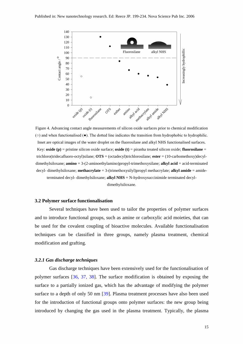
3.1.3 Surface wettability – an example of one effect of indirect chemical modification
As an example of the change in physical properties, functionalisation can be
used to drastically alter the surface wettability of a substrate. Via careful choice of
functionalisation groups with different termination moieties, the hydrophobicity of the
surface can be “tuned”. For example, the contact angle of a water droplet on the surface
of a silicon oxide surface can be altered between 30° and 130°, from hydrophilic to
hydrophobic respectively, by the addition of various silane-based functionalised
molecules (Figure 4).
Published in: New nanotechnology research. Ed: Reece JP. 199-234. Nova Science Pub Inc. 2006
15
Incr
easi
ngly
hydro
phil
lic
oxid
e (p
)
oxid
e (t)
fluor
osila
neO
TS
esth
er
amin
o
alky
l aci
d
met
hacr
ylat
e
alky
l am
ide
alky
l NH
S
Conta
ct a
ngle
/ o
0
10
20
30
40
50
60
70
80
90
100
110
120
130
140
Fluorosilane alkyl NHS
Figure 4. Advancing contact angle measurements of silicon oxide surfaces prior to chemical modification
(○) and when functionalised (●). The dotted line indicates the transition from hydrophobic to hydrophilic.
Inset are optical images of the water droplet on the fluorosilane and alkyl NHS functionalised surfaces.
Key: oxide (p) = pristine silicon oxide surface; oxide (t) = piranha treated silicon oxide; fluorosilane =
trichloro(tridecafluoro-octyl)silane; OTS = (octadecyl)trichlorosilane; ester = (10-carbomethoxy)decyl-
dimethylsiloxane; amino = 3-(2-aminoethylamino)propyl-trimethoxysilane; alkyl acid = acid-terminated
decyl- dimethylsiloxane; methacrylate = 3-(trimethoxysilyl)propyl methacrylate; alkyl amide = amide-
terminated decyl- dimethylsiloxane; alkyl NHS = N-hydroxysuccinimide terminated decyl-
dimethylsiloxane.
3.2 Polymer surface functionalisation
Several techniques have been used to tailor the properties of polymer surfaces
and to introduce functional groups, such as amine or carboxylic acid moieties, that can
be used for the covalent coupling of bioactive molecules. Available functionalisation
techniques can be classified in three groups, namely plasma treatment, chemical
modification and grafting.
3.2.1 Gas discharge techniques
Gas discharge techniques have been extensively used for the functionalisation of
polymer surfaces [36, 37, 38]. The surface modification is obtained by exposing the
surface to a partially ionized gas, which has the advantage of modifying the polymer
surface to a depth of only 50 nm [39]. Plasma treatment processes have also been used
for the introduction of functional groups onto polymer surfaces: the new group being
introduced by changing the gas used in the plasma treatment. Typically, the plasma
Published in: New nanotechnology research. Ed: Reece JP. 199-234. Nova Science Pub Inc. 2006
16
treatment can change the surface chemistry and the wettability of the polymer surface,
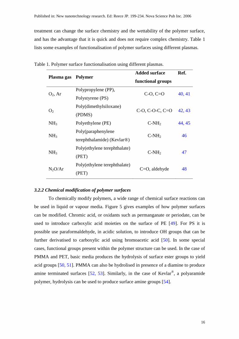
and has the advantage that it is quick and does not require complex chemistry. Table 1
lists some examples of functionalisation of polymer surfaces using different plasmas.
Table 1. Polymer surface functionalisation using different plasmas.
Plasma gas Polymer Added surface
functional groups
Ref.
O2, Ar Polypropylene (PP),
Polystyrene (PS) C-O, C=O 40, 41
O2 Poly(dimethylsiloxane)
(PDMS) C-O, C-O-C, C=O 42, 43
NH3 Polyethylene (PE) C-NH2 44, 45
NH3 Poly(paraphenylene
terephthalamide) (Kevlar®) C-NH2 46
NH3 Poly(ethylene terephthalate)
(PET) C-NH2 47
N2O/Ar Poly(ethylene terephthalate)
(PET) C=O, aldehyde 48
3.2.2 Chemical modification of polymer surfaces
To chemically modify polymers, a wide range of chemical surface reactions can
be used in liquid or vapour media. Figure 5 gives examples of how polymer surfaces
can be modified. Chromic acid, or oxidants such as permanganate or periodate, can be
used to introduce carboxylic acid moieties on the surface of PE [49]. For PS it is
possible use paraformaldehyde, in acidic solution, to introduce OH groups that can be
further derivatised to carboxylic acid using bromoacetic acid [50]. In some special
cases, functional groups present within the polymer structure can be used. In the case of
PMMA and PET, basic media produces the hydrolysis of surface ester groups to yield
acid groups [50, 51]. PMMA can also be hydrolised in presence of a diamine to produce
amine terminated surfaces [52, 53]. Similarly, in the case of Kevlar®, a polyaramide
polymer, hydrolysis can be used to produce surface amine groups [54].

Published in: New nanotechnology research. Ed: Reece JP. 199-234. Nova Science Pub Inc. 2006
17
* CH2
CH2 *
n
* CH2 *
n
CH3
OO
CH3
PE
PS
PMMA
* CH2
CH *n
OH
* CH2
CH2 *
n
O
O
OH
* CH2
CH *n
* CH2
CH *n
OH
* CH2
CH *n
O
O
OH
* CH2 *
n
CH3
OOH
* CH2 *
n
CH3
ONH
NH2
* O
O O
O CH2
CH2 *
n
O
O O
OH OH CH2
CH2
* CH2
CH *n
O
SiCH3R
PDMS OSi
OSi
CH3 CH
3
CH3
CH3
n
O
SiO
Si
OH CH3
R1CH
3
n
R1= OH, COOH
O
SiR2
OSi
OSi
CH3
R1CH
3
n
R= COOH
PET
O
H H
NH2
NH2
n n
CrO3
AcOH/Ac2O
AcBr/NaOH
ClSi(CH3)2R
AcOH
AcBr/NaOH
i) NaOH
ii) HCl
6
Borate buffer pH: 11.5
O2 plasma ClSi(CH3)2R2
i) NaOH
ii) HCl
6
Figure 5. Examples of the surface modification of PE, PS, PMMA, PET and PDMS by chemical means to
produce functionalised polymer surfaces with active chemical moieties.
A combination of the previous methods (i.e. plasma treatment and chemical
functionalisation) allows further modification of the surface of the polymer, e.g. for the
addition of a silicon-based layer to the polymer surface. PDMS and PE can initially be
treated with O2 plasma to introduce OH groups on the surface. Post plasma treatment
exposure of the surface to an alkyltrichlorosilane vapour causes the silane to form a
monolayer film on the polymer surface. This introduction of OH groups on the polymer
surfaces and subsequent treatment with the silane is similar to the reactions commonly

Published in: New nanotechnology research. Ed: Reece JP. 199-234. Nova Science Pub Inc. 2006
18
used to treat silicon oxide surfaces. Similarly, SiCl4 can be used to produce a
homogenus layer of silicon oxide over plasma oxidized PE [55]. The surface of this
layer has a low roughness, is densely and uniformly functionalised, and provides
functional groups that can be used in the formation of alkylsiloxanes SAMs on the
polymer surface.
3.2.3 Grafting
Several methods exist for the grafting of chemical functionality to a polymer
surface. Typically, free radicals or peroxides are formed at the polymer surface by
exposing it to alpha radiation, electrons, UV radiation, plasma or ozone, or via chemical
treatment [56, 57]. The energetic active sites that are formed are then used as surface
bound initiators which initiate grafting reactions with unsaturated compounds that
contain the desired functionality (Figure 6). For example, UV radiation has been used to
activate a PDMS surface to introduce by graft polymerisation acrylic acid, acryl amide,
dimethyl acrylamide, and 2-hydroxyethyl-acrylate [58]. Unfortunately, grafting
processes suffer from the production of polymer residues which can be formed by the
unsaturated compounds, and which may cause problems post-functionalisation unless
they are removed.
ROHROH
X
R
OH
R* R*R*
X
R*R*
C*
X
RR* R*R*
H2OUV
Figure 6. An example mechanism of the grafting of a molecule with a functionalised moiety (X) to a
polymer surface. R* is an excited moiety on the polymer surface.
3.3 Functionalised layer characterisation
In addition to the techniques mentioned in section 2.3, several methods are
available to physically characterise surfaces that have been subjected to surface
modification, i.e. with respect to layer thickness and surface coverage. Optical
techniques used to characterise thin films on flat substrates include ellipsometry [59],
scanning near-field optical microscopy (SNOM) [60] and surface plasmon resonance
(SPR) [61]. The ellipsometer reflects light of known polarization off a sample surface,
and measures the polarization change upon reflection. The exact nature of the
polarization change is determined by the sample's properties (e.g. thickness and
Published in: New nanotechnology research. Ed: Reece JP. 199-234. Nova Science Pub Inc. 2006
19
refractive index). Although optical techniques are inherently diffraction limited,
ellipsometry exploits phase information and the polarization state of the light, and can
achieve Angstrom resolution. The technique is applicable to films with thicknesses from
less than a nanometre to a micrometer, and is used to study the formation of monolayers
on substrates and how the layer thickness of absorbed protein layers depends on the
surface chemical properties [62].
Near-field optical imaging involves illuminating a surface through a sub-
wavelength sized aperture. The surface is positioned within the near-field regime of the
source, in an area where the radiation from the source does not have the opportunity to
diffract before it interacts with the sample. The resolution of the system is therefore
determined by the aperture diameter, as opposed to the wavelength of light used. For
example, if white light is used, sub-200 nm resolution can now be achieved, a resolution
unobtainable using far field optical microscopy [63].
The SPR uses the evanescent field created by a beam of light shining on the
surface of a thin metallic layer to measure the thickness of thin layers deposited on the
metal surface. Light energy, from the incident light, interacts with the delocalised
electrons in the metal film (plasmon) thus reducing the reflected light intensity. As a
functional layer is added to the immobilised surface, the local refractive index changes,
leading to a change in the angle of the surface plasmon resonance. This can be
monitored by detecting changes in the intensity of the reflected light. The rates of
change of the SPR signal can be analysed to yield apparent rate constants for the
association and dissociation phases of the reaction. Thus the thickness of the added film
can be calculated. As the SPR signal depends only on binding to the immobilised
template, it is also possible to study binding events from biomolecules from
heterogeneous solutions [64].
Other techniques that can be used to study the physical properties of
functionalisated surfaces include x-ray photoelectron spectroscopy (XPS), and time-of-
flight secondary ion mass spectrometry (TOF-SIMS), both of which also provide
information on the chemical composition of the surfaces.
XPS is a non-destructive, surface sensitive technique that provides quantitative,
surface chemical state information for all elements except hydrogen and helium [65].
The sample is irradiated with a beam of monochromatic soft X-rays causing
photoelectron emission to occur from the atoms in the sample. The distribution of
kinetic energies from the sample is then directly measured by the electron spectrometer.

Published in: New nanotechnology research. Ed: Reece JP. 199-234. Nova Science Pub Inc. 2006
20
Atomic orbitals from atoms of the same element in different chemical environments are
found to possess different binding energies. Differences in oxidation state, molecular
environment and co-ordination number all provide different chemical shifts.
Photoelectron binding energy shifts are, therefore, the principal source of chemical
information. It should be noted that these shifts can be very small and can only be
detected using a high performance instrument with suitable software. Layer thickness
can be measured to a depth of 10 nm.
TOF-SIMS uses a pulsed primary ion beam to desorb and ionise species from a
sample surface [66, 67]. The resulting secondary ions are accelerated into a mass
spectrometer, where they are mass analyzed by measuring their time-of-flight from the
sample surface to the detector. An image can be generated by rastering a finely focused
beam across the sample surface. Due to the parallel detection nature of TOF-SIMS, the
entire mass spectrum is acquired from every pixel in the image. The mass spectrum and
the secondary ion images are then used to determine the composition and distribution of
sample surface constituents. Depth information is produced by removing successive
layers of material from the surface which can be used to build up a 3-D map of the
material under study. Unfortunately, this does mean that the technique is destructive.
Other techniques can be used to produce further information about the chemical
and physical nature of the surface [68]. Some examples are given in Table 2.
Table 2. Examples of some techniques for the characterisation of surfaces
Technique Surface characteristic
Various spectroscopies
(e.g. FTIR, Raman, UV/visible)
Chemistry
X-ray photoelectron spectroscopy Chemical structure/electrical properties
Transmission electron microscopy Atomic structure
Contact angle measurement Wettability/Surface energy
3.4 Protein immobilisation - an example of an application for chemically
functionalised surfaces
Modelling of the adsorption of proteins to surfaces with different functional
groups approximately correlates with the surface hydrophobicity. The protein can be
reversibly attached to the surface via hydrophobic or electrostatic interactions. These
Published in: New nanotechnology research. Ed: Reece JP. 199-234. Nova Science Pub Inc. 2006
21
interactions are the most common and experimentally the simplest, but they are difficult
to control and normally have no positional directionality. The adsorption on
hydrophobic surfaces is often kinetically irreversible. However, the protein layer can be
removed using detergents or replaced by other proteins with a higher affinity for the
surface [69]. This is advantageous when proteins are to be substituted, but
disadvantageous when the protein layer is to remain in place.
Methods that rely on covalent coupling of proteins to surfaces are inherently
more controllable and give layers of protein that cannot dissociate from the surface or
exchange with other proteins in solution. The most successful techniques for attachment
of proteins using covalent immobilisation have been based on the formation of amide
and disulfide bonds [70]. Unfortunately, one problem that can occur when the protein is
immobilised is protein denaturation, which consequently causes a loss in protein
activity. A remedy for this problem has involved coupling of the protein to “inert”
materials, such as oligo(ethy1ene glycol) terminated SAMs.
The biospecific adsorption of proteins to SAMs is important for biological
applications, such as chromatography, cell culturing, the production of artificial
implants and organs etc. Typically, the target protein must be allowed to interact with
the surface, to the exclusion of all other proteins. A common immobilisation technique
is based on the biotin-streptavidin interaction [71, 72]. The effectively irreversible
complex formed in this system is useful for many applications, including the
immobilisation of proteins. The strepavidin allows the introduction of anti-biotin sites
on the surface [73], which can be used to introduce a wide range of biotinylated
biomolecules, such as the reversible binding of lactate dehydrogenase to SAMs that
present analogues of nicotinamide adenine dinucleotide (NAD) [74, 75], and the
recognition of immobilised antigen by antibodies [76].
Contrary to surfaces for the immobilisation of protein, materials that resist the
adsorption of proteins have also been investigated [69]. An efficient technique for
producing a protein resistant surface has been to use poly(ethy1ene glycol) (PEG)
layers, which can be produced by adsorption, covalent immobilisation, or radiation
cross-linking. Polymers with carbohydrate moieties in their conformation can also be
used, but the addition of PEG is ultimately the most efficient polymer-based technique.
Another available method is to use a “blocking” protein, such as bovine serum albumin
(BSA). Unfortunately, such proteins tend to denature over time, or exchange with other
proteins in solution, allowing unwanted protein access to the surface.
Published in: New nanotechnology research. Ed: Reece JP. 199-234. Nova Science Pub Inc. 2006
22
3.5 Summary
Polymers present a wide range of surface functionalisation possibilities. These
can be used to alter the surface properties of the polymer itself, or by the
implementation of an additional functional layer, or can be used to add chemical or
biological functionalisation. The possibility of patterning such chemical
functionalisation and utilising more than one functional species, using such techniques
as micro-contact printing or dip pen lithography, opens up a number applications within
array and sensor production applications.
4. BIOMEDICAL APPLICATIONS
Both micro- and nanostructured surfaces have been found to affect the growth of
cells cultured on the surface. Inorganic materials that have been used for
topographically structured surface interactions with cells include elements, such as gold
and silicon, and compounds, mainly based on silicon: organic surfaces are normally
based on polymers [77]. Important characteristics that must be defined when attempting
to examine cell-surface interactions depend on the topographical properties, including
structure depth, groove width etc., and the chemical/physical properties of the surface,
such as hydrophobicity etc. The latter substrate characteristics are doubly important if
the surface has been functionalised. The interaction between the cell and the surface can
then be characterised by examining properties such as whether the cell can be made to
grow on the structured surface, whether the cell propagates, how the cell orientates itself
with respect the surface structures, and whether any physical or chemical changes occur
in the cell, e.g. elongation [1, 78]. For tissue forming applications, these considerations
are joined by the obvious need for the cells to form tissue structures with neighbouring
cells, e.g. for tendon repair [79]. The applications for such structures can be grouped
into a number of categories, namely those for imaging, those for adhesion, proliferation
and differentiation, those for cellular structuring, and those for tissue formation.
4.1 Imaging
Transparent substrates are a preferred choice for use in a biomaterials research
laboratory, a precursor to general use in the field of biomedicine. Current techniques
used in biology become awkward when they have to be applied to biomaterials
applications. To evaluate the biocompatibility of materials, a quantitative evaluation of

Published in: New nanotechnology research. Ed: Reece JP. 199-234. Nova Science Pub Inc. 2006
23
cell adhesion and proliferation generally implies the detachment of cells from a surface.
However, it is very important to follow the culturing of the cells over time without
interfering with or destroying the cells. The use of transparent polymers allows the
researcher to study cell behaviour by means of an inverted optical microscope, the most
common technique available in cell biology labs, and record the changes in cell
morphology during adhesion, mobility and proliferation. Such transparent polymers can
be preferred to glass as it is possible to functionalise and structure the surface to trigger
specific cell responses.
4.2 Adhesion, proliferation and differentiation
Cell adhesion to surfaces in the biomedical domain implies two distinct phases.
Firstly, the attachment of the cell to the surface, which occurs rapidly and involves
physicochemical linkages between cells and materials by means of ionic forces, van der
walls forces, etc. Second is the adhesion of the cell to the surface which it has become
attached. This occurs over a longer time span and involves biological molecules, such as
extracellular matrix (ECM) proteins, cell membrane proteins and cytoskeleton proteins,
which interact together to induce signal transduction, promoting the action of
transcription factors and consequently regulating gene expression [80].
Good interactions between cells and the surfaces of materials are highly relevant
and contribute to the clinical success of implants. Surface characteristics, such as
topography, chemistry and surface energy, determine whether the adhesion between cell
and surface is good, and hence whether subsequent proliferation and ECM production
occur to form new tissue. Individually, these characteristics establish how biological
molecules will absorb to the surface and in what orientation. Thus, they determine cell
behaviour and proper tissue formation.
The organization of surface roughness is an important parameter. In-vitro,
several authors have determined the effect of grooves and ridges to orientate epithelial
cells and fibroblasts. Orientation has also been observed in osteoblasts. Osteoblasts
cultured on Ti surfaces with microrough features exhibit reduced proliferation and
enhanced differentiation when compared to cells grown on tissue culture plastic or
smooth Ti substrates [81]. In vivo, surface roughness may control tissue healing and
enhance implant success [82, 83] However, in vivo studies have failed to demonstrate
differences in bone-to-implant contact between comparable roughness parameters
performed using different techniques. On the other hand, recent studies using dental

Published in: New nanotechnology research. Ed: Reece JP. 199-234. Nova Science Pub Inc. 2006
24
implants with a good control of the surface roughness at the microscale exhibit
increased pull-out strength. The microtopography of the implant in the study included a
mixed morphology of craters and micropits [84, 85].
4.3 Cellular structuring
Micropatterned surfaces can be used to understand how cells respond to specific
structural features. Micrometer and/or nanometer scale topographies affect different
aspects of cell behaviour, including such characteristics as cell adhesion, cell
proliferation, cell differentiation, cell morphology, cell orientation, contact guidance,
tissue organization, etc. [77, 80, 86, 87, 88]. Depth and width of grooves can determine
how cells in the osteoblast lineage form focal contacts and how they produce and
mineralize the ECM [89, 90]. However, the response of osteoblasts to microstructures
cannot be considered without also considering the surface chemistry. Cell response
cannot be predicted from studies performed on different materials albeit with the same
surface architecture.
The production of surfaces with a well defined microarchitecture will facilitate
the study of cell behaviour when it is essential to design materials capable of
modulating cell response. For example, a study has demonstrated that cell attachment
depends on cavity spacing, cell growth depends on cavity dimensions, and cell
morphology depends on the presence of sub-micron-scale structural features [81].
Another study, performed on titanium surfaces with increasing surface roughness,
concluded that osteoblasts do not react to 10 m diameter cavities, simply sitting on top
of them. However, cells were seen to enter 30 m and 100 m cavities and adopt
different morphologies: adopting a 3-D shape within the 30 m cavities but a more
flattened one within the 100 m cavities [91].
With regards nanostructured topographies, different cell types have been shown
to react differently to different nanostructures [77]. One consequence of this is that the
cell morphology on the submicrometer scale favours the formation of long and
numerous filopodium [91]. However, there is probably a limit to the feature size to
which the cell is sensitive. For example, Scotchfold et al. presented a study on
chemically patterned surfaces and observed that osteoblasts did not react to nanometric
surfaces (20 nm) on Ti/Ti surfaces [92]. Even so, it is obvious that the behaviour of

Published in: New nanotechnology research. Ed: Reece JP. 199-234. Nova Science Pub Inc. 2006
25
cells is greatly influenced by the micro- and nanotopography, singly or in combination,
of surfaces.
4.4 Tissue formation
Tissue engineering is a growing field within biomedical research. The
optimisation of the surface topography and chemistry of materials is designed to induce
a faster adhesion of cells and a more efficient production of ECM, for healing wounds
for example. The biomaterials used to aid tissue regeneration have to have several
characteristics, including biocompatibility, and tissue conducting and tissue inducing
properties. The use of polymers, in the case of bone engineering for example, is an
interesting option. The use of biodegradable materials especially offers several
advantages over the metals and other non-degradable materials used at present as
orthopaedic implants. Firstly, they do not have to be removed after implantation,
negating the requirement for a second surgical procedure and avoiding possible
complications. Secondly, such polymers are easy to load with growth factors which can
be used to increase cell growth and bone formation. Finally, they are liable to surface
modifications to control their surface properties and consequently direct cellular
adhesion and cellular response [80, 93]. Together with the possibility of fabricating
composite materials, with organic molecules such as collagen or cells, these materials
are a potential solution for bone grafting requirements.
Amongst other applications, besides bone grafting and regeneration,
biodegradable polymer stents are currently being researched for use in cardiology [94]
and urinary applications [95].
5. RAPID REPLICATION TECHNIQUE
Briefly, our technique for the production of structured polymer surfaces consists
of a number of well defined steps. Topological structuring is achieved using polymer
embossing. An inorganic mould is produced and used to emboss the polymer at elevated
temperature and pressure to impart topography. Chemical patterning is achieved using
micro-contact printing. A similar mould to that used for embossing is used to produce
an elastomeric stamp. This is inked with the required functionalising molecules and then
used to transfer these molecules to the polymer surface in areas where the stamp and
polymer make conformal contact. In each case, the patterned polymer surfaces are used

Published in: New nanotechnology research. Ed: Reece JP. 199-234. Nova Science Pub Inc. 2006
26
to examine their interaction with cells. The details of each of the production steps are
outlined in the following sections.
5.1. Silicon mould fabrication
Silicon moulds were produced using a previously described method [96]. For the
microstructured surfaces, designs utilised included several types of surface structures,
with dimensions ranging from 1 m2 to 100 m
2 (i.e. 10x10 m
2). The microstructures
were defined in the mould surface to give moulds with positive superficial structures
(where the features are higher than the surface) or negative superficial structures (where
the features are lower than the surface). In total, the repeated microstructures cover an
area of 1 cm2.
Production of moulds in silicon oxide (SiO2) and silicon nitride (Si3N4) was
completed using two different fabrication methods depending on the height of the
required structures. The first method involved the growth of layers of oxide and nitride
on the surface of a silicon wafer previously patterned using deep reactive ion etching
(DRIE). This allowed relatively tall (~1 m) structures to be produced. In the case of
the Si3N4 moulds, an underlying SiO2 layer is necessary to compensate for the intrinsic
stress in the thermally evaporated layers.
The second method for fabrication of the SiO2 and Si3N4 moulds involved
thermally growing oxide or nitride layers on a pristine silicon wafer, prior to
photolithographic patterning and DRIE. This technique limited the height of the
structures to the thickness of the deposited layers. In addition to these fabrication
conditions, each mould was produced in two further configurations; one using the
original 500 nm thick silicon wafer, modified as described above, and one where the
500 nm thick silicon wafer is anodically bonded to a 1 mm thick pyrex wafer, prior to
modification, to increase the strength, and hence the lifetime, of the mould.
Further mould production was possible by modification of the unstructured
silicon-based substrates, or the previously described microstructured moulds, with the
introduction of micro- or nanostructures using FIB milling. The FIB (Strata DB235; FEI
Co., Netherlands) apparatus could be used to mill structures into the raised structures on
the original mould, or to create new patterns on the unstructured substrates. Figure 7
gives an example of a microstructured master that has been modified using FIB.

Published in: New nanotechnology research. Ed: Reece JP. 199-234. Nova Science Pub Inc. 2006
27
Figure 7. SEM image of a silicon substrate containing 400 nm tall, 5x5 m2 microstructures, some of
which have been modified using FIB milling [bar = 20 m].
The SiO2/Si3N4 layers on the mould surface were used to prevent adherence
problems between the mould and the polymer; however, after surface modification
using the FIB a fluoroalkylsilane monolayer (trichloro(tridecafluoro-octyl)silane;
United Chemical Technologies, USA), was sometimes added to eliminate any sticking
problems. The fluoroalkysilane was deposited from the liquid phase using a previously
described method [97]. Once prepared, the moulds could be used either for
micro/nanoembossing or for the preparation of stamps for micro-contact printing.
5.2. Polymer embossing
Polymer embossing was achieved via nanoembossing using a commercially
available nanoimprinter [2.5‟ Nanoimprinter, Obducat AB, Sweden.]. Normally the
polymer used for the embossing is spun down onto the surface of a suitable substrate;
commonly a piece of the material used to produce the mould. The mould is then placed
in contact with the polymer surface and the embossing proceeds in a typical fashion
[98]. This has the disadvantage that the embossed substrate is no longer transparent, and
hence less useful for biomedical applications. To remedy this, we have developed a
method for producing freestanding, embossed polymer films with high transparency
[99, 100].
The polymer embossing has been achieved in 125 m thick sheets of PMMA
(Goodfellow Ltd., UK). For each experiment, the polymer was cut to the approximate
size of the mould to be used for the embossing. The polymer was rinsed with
isopropanol (IPA, Aldrich Chemical Co., UK), to remove any dust particles, and dried

Published in: New nanotechnology research. Ed: Reece JP. 199-234. Nova Science Pub Inc. 2006
28
using a stream of nitrogen gas.
A schematic diagram of the nanoembossing process is given in figure 8. The
silicon mould is placed onto the base of the nanoimprinter with the structured surface to
be embossed uppermost. The polymer sheet is then placed on top of the mould, with the
surface to be embossed in contact with the mould. They are then both covered with a
second sheet of polymer (e.g. Teflon®) with a glass transition temperature (Tg) higher
than that of the polymer to be embossed. The Teflon® is used to eliminate any
patterning of the backside of the polymer by the thin aluminium sheet used to hold
everything in place in the apparatus (Figure 9). A drawback to this technique is that the
back side of the PMMA is slightly wavy, possibly suggesting an uneven applied
pressure. This does not however affect the surface being embossed and could be
rectified by using a thicker piece of Teflon®, which should distribute the pressure more
evenly.
1
234
Figure 8. Schematic diagram of the embossing process used to produce freestanding polymer films
containing micro/nanostructures. The PMMA (2) is sandwiched between the mould (1) and the
aluminium (4) used in the nanoimprinter. The PMMA is protected by a high Tg polymer (3, see text).
Figure 9. Elimination of backside patterning of 125 m thick PMMA sheets through the use of a high Tg
polymer layer. In (a) the PMMA (2) is only sandwiched between the mould (1) and the aluminium (4). In
(b) the PMMA is protected by the high Tg polymer (3). In each case, the optical images show the surface

Published in: New nanotechnology research. Ed: Reece JP. 199-234. Nova Science Pub Inc. 2006
29
patterning by the mould on the front side of the polymer (A) and the presence (or absence) of the
patterning by the aluminium on the reverse (B).
An example of the process graph for the nanoembossing is given in figure 10.
The system is first warmed up using two heating steps, A. The polymer is then heated,
B, to a temperature above that of the polymer Tg, causing the polymer to soften. Once
the temperature has stabilised, the mould is forced into the surface of the polymer under
pressure, C, which forces the polymer to fill the structures in the patterned mould. After
a period of time the polymer fills the structures completely. The embossed polymer film
is then cooled, D, to a temperature below that of Tg. This forces the polymer to adopt
the shape imparted by the mould. Finally, the pressure is removed, E, and the polymer
and the mould can be removed from the apparatus. After a short period of cooling (~5
min), outside the press system, the embossed polymer sheet can simply be manually
demoulded from the surface of the mould. (Note: after the system is warmed up, prior to
the first embossing step, the warm up steps, A, do not need to be repeated.)
Pre
ssu
re /
bar
0
10
20
30
40
50
60
70
Time / s
0 1000 2000 3000
Tem
per
ature
/ o
C
40
60
80
100
120
140
Tem
per
ature
/ o
C
40
60
80
100
120
140
Pre
ssu
re /
bar
0
10
20
30
40
50
60
70
(a)
(b)
(c)
(d)
A
C EB D

Published in: New nanotechnology research. Ed: Reece JP. 199-234. Nova Science Pub Inc. 2006
30
Figure 10. A typical example of a process graph for nanoembossing where (a) is the emperature set point,
(b) is the recorded temperature, (c) is the pressure set point, and (d) is the recorded pressure (See text for
details).
In this example, the total embossing time is ~20 minutes at 60 bar pressure.
However, these process parameters can be reduced or increased depending on the type
of polymer, the mould material and the dimensions of the structures to be produced. We
have already applied this technique to freestanding polymer sheets of PMMA, PLA
[100], and poly(ethylene naphthalate) (PEN) but it should be applicable to a wide range
of thermoplastic polymers.
5.3 Polymer replica characterisation
PMMA replicas fabricated by embossing techniques have been characterised
using some of the aforementioned characterisation methods. Imaging of the surfaces of
the moulds and the patterned polymers has been achieved using optical microscopy,
white light interferometry (Wyko NT110; Vecco Metrology, USA.), atomic force
microscopy (Pico Plus; Molecular Imaging, USA), and scanning electron microscopy
(SEM: Strata DB235; FEI Co., Netherlands.), depending on the size of the structures, or
the substrate material, to be imaged. AFM measurements show that the pristine PMMA
was found to have a typical surface roughness (ra) of ~13 nm. Embossing of the
polymer introduces structures into the surface of the polymer and consequently
increases the roughness. An example of some regular microstructures embossed in
PMMA is given in figure 11: examples of regular nanostructures embossed in PMMA
are given in figure 12.

Published in: New nanotechnology research. Ed: Reece JP. 199-234. Nova Science Pub Inc. 2006
31
Figure 11. SEM images of regular microstructures, with dimensions of (a) 10 m diameter, (b) 5 x 5 m2,
(c) 2.5 m diameter and (d) 1 m diameter, and ~400 nm tall, embossed in a 125 m thick freestanding
PMMA sheet, over an area of 1 cm2.
Figure 12. AFM and SEM images of regular nanostructures embossed in PMMA with dimensions of (a)
200 nm wide, 100 nm tall, 80 m long lines, and (b), 200 nm tall, 1 m diameter posts embossed on two
levels of a 400 nm tall step. The aspect ratio of the lines in the bottom left hand corner of the SEM image
in (a) was too high and hence they have collapsed [bar = 5 m].
The wettability of the polymer surface was characterised using contact angle
measurements both before and after embossing (Figure 13), and compared to soda lime
silicate glass (commonly used in biological laboratories as microscope slides) and
silicon nitride (the mould material). The advancing contact angles (water, 0.3 ml) give
an idea of the hydrophobicity of each surface. The PMMA surface, when unstructured,

Published in: New nanotechnology research. Ed: Reece JP. 199-234. Nova Science Pub Inc. 2006
32
is slightly more hydrophilic than the silicon nitride, but less so than the glass. The
advancing contact angle of PMMA is seen to increase from 73.4°, a value that agrees
with previously published results [101, 102], to 74.7°, upon sterilisation with gamma
radiation (see section 5.4). A similar small increase, from 75° to 81°, has been found
after gamma irradiation of poly(caprolactone) (PCL) surfaces, and has been attributed to
a slight oxidation of the surface via free radicals produced during the irradiation [103].
The advancing contact angles for the glass, 35.0°, and silicon nitride, 73.0°, also
approach those recorded in the literature, i.e. 40° [104] and 85.9° [105] respectively.
However in these cases, the hydrophobicity of the samples was seen to increase more
dramatically (by more than 10° in each case). Again this may be due to oxidation of the
surface after the irradiation and, as the surface material is more densely packed
compared to the PMMA, the effect is more pronounced.
Figure 13. Advancing (filled symbols) and receding (open symbols) water (0.3 ml) contact angle
measurements of PMMA surfaces: also shown for comparison are measurements for glass and silicon
nitride (Si3N4).
Key: (u) unsterilised, non-structured; (s) sterilised, non-structured; (pos) sterilised, positively structured
with 5 m2, 400 nm tall posts; (neg) sterilised, negatively structured with 5 m
2, 400 nm deep holes.
Interestingly, upon microstructuring the PMMA, the surface becomes
increasingly hydrophobic. This effect has also been observed for PEN, although in this
case the contact angle was found to decrease upon structuring the polymer surface [99].
The contact angle hysteresis, the difference between the advancing and receding

Published in: New nanotechnology research. Ed: Reece JP. 199-234. Nova Science Pub Inc. 2006
33
contact angles, gives a value for the surface wettability, which in turn gives an idea of
the roughness of the surface. Measuring the receding contact angle for the sterilized
PMMA (63.2°) gives a H2O contact angle hysteresis of ~12°, a value indicative of a low
surface roughness, which is consistent with the result obtained through the AFM
measurements. As expected, when the PMMA is microstructured, the hysteresis
increases due to the increased surface roughness introduced onto the polymer surface by
the structuring. Upon sterilisation, the hysteresis of the PMMA decreases by 9°,
suggesting a decrease in surface roughness, possibly due to some local surface etching
or melting [103]. Similarly, there is a slight increase in the hysteresis for the glass,
suggesting an increase in surface roughness, but no change in the values for silicon
nitride.
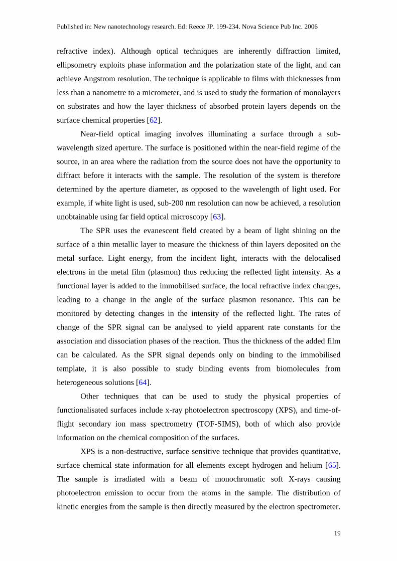
The optical transmission of pristine PMMA and PEN has been measured [99], in
the range 300 to 800 nm, and compared with that of a 1.5 m thick, soda lime silicate
glass cover slip (Figure 14). PMMA is seen to have an optical transparency rivalling
glass throughout the near IR/visible region of the electromagnetic spectrum. Although
this transmittance decreases in the UV region of the spectrum, the polymer still
transmits some 60% of the incident light at a wavelength of 300 nm. PEN in
comparison transmits ~80% of the incident light in the near IR/visible region, but its
transmission falls rapidly as the UV region is encountered at ~400 nm, due to the
presence of the UV-adsorbing naphthalene moiety in the polymer matrix. The addition
of structures to one surface of the polymer does decrease the transmittance (by as much
as 20%), but the samples are still sufficiently transparent to be used with optical
microscopes commonly found in a biological laboratory.
Published in: New nanotechnology research. Ed: Reece JP. 199-234. Nova Science Pub Inc. 2006
34
Wavelength / nm
300 400 500 600 700 800
Tra
nsm
itta
nce
/ %
0
20
40
60
80
100
Nanotechnology © copyright (2005) IOP Publishing Ltd.
Figure 14. Optical transmission spectra of glass (solid curve), PMMA (dashed curve) and PEN (dash/dot
curve) at wavelengths close to the visible region of the electromagnetic spectrum, showing the percentage
of visible radiation transmission for each, compared to an air blank, and the near-UV absorption of each
sample [99].
5.4 Sterilisation
To ensure the sterility of the polymers prior to use in in-vitro culturing
experiments, a number of sterilisation techniques commonly used for the sterilisation of
apparatus used in biological experiments, were investigated with varying degrees of
success. Due to the low heat tolerance of the PMMA samples, the typical sterilisation
temperatures (~120°C) used in an autoclave caused the PMMA to deform and caused
the structures on the surface to melt. The low solvent tolerance of the PMMA caused
similar effects when the PMMA was immersed in 70% ethanol (although the polymer
showed no adverse effects after rinsing with propan-2-ol). To sterilise the PMMA
samples we therefore turned to UV and gamma ray sterilisation. Gamma ray
sterilisation, at 25 kGrays dose, was preferred due to the possibility of UV light
affecting the chemical structure of the polymer. AFM and contact angle measurements
confirmed that the surface roughness and wettability of the PMMA did not change,
suggesting that the sterilisation did not affect the physical and chemical structure of the
polymer surface to any great degree.
Although neither the ethanol immersion nor the autoclaving techniques were
suitable for PMMA structured surfaces, they could be used with more robust polymers,
such as PEN. A structured PEN film was initially cleaned and sterilised using gamma

Published in: New nanotechnology research. Ed: Reece JP. 199-234. Nova Science Pub Inc. 2006
35
radiation. The surface of the polymer was then used to culture MG63 osteoblast cell line
for 7 days using an established technique [106]. After this, the PEN was thoroughly
cleaned and re-sterilised by immersion in 70% ethanol. The sterilised PEN was then
placed in culture medium in the absence of cells to examine whether any growth
occurred. After a further 7 days, no osteoblast cell growth was observed and the
chemical sterilisation was assumed to be successful. This suggests that PEN films can
be re-used for culturing of MG63 cells as long as thorough sterilisation is performed
between culturing experiments. The PEN has this advantage over PMMA due to its
higher chemical resistivity. This allows it to be immersed in the 70% ethanol without
degradation or deformation of the structures in the polymer surface.
5.5 Chemical functionalisation of polymer surfaces
Chemical functionalisation of the surface of PMMA substrates has also been
achieved using a variety of SAM molecules. These have been further chemically
modified to add such linking molecules as required for activation with biological
moieties, or to change the surface properties. The functionalisation has been patterned
by using microcontact printing [107]. For example, the PMMA surface was
functionalised with a biotin pattern (Figure 15). The PMMA is first hydrolysed, 1, and
activated by the addition of PFP/EDC, 2. The biotin pattern is then added via a PDMS
stamp that has been immersed in Biotin-EZ (Culteck). The biotin only attaches to the
surface in areas of mutual contact between the stamp and the surface, 3. The areas not
patterned with the biotin are then blocked using 2-(2-aminoethoxy)ethanol to avoid non
specific adsroption in these areas, 4. The pattern was imaged by exposing it to a solution
of Texas red-labelled streptavidin. The streptavidin links to the biotin coated areas and
the pattern can be imaged via fluorescence spectroscopy (Figure 16).

Published in: New nanotechnology research. Ed: Reece JP. 199-234. Nova Science Pub Inc. 2006
36
Figure 15. Scheme showing the selective patterning of a PMMA surface with biotin (see text for details).
Figure 16. A PMMA surface functionalised with a biotin pattern using a microcontact printing technique.
This pattern was subjected to Texas Red dye, and imaged using fluorescence microscopy.
5.6 Biomedical applications of patterned polymer surfaces
The first requirement of polymer substrates that are to be used for in-vitro cell-
surface interactions is to withstand culture solutions and to support growth of the cells
on the (structured) surface. Fortunately, in the first case, as most cell lines are sensitive
to harsh environmental conditions, most culture solutions are based on aqueous
solutions buffered to around physiological pH levels (i.e. ~pH 7 [108]). They are
normally used at temperatures close to those found in the body (~37°C), and contain
little more than dissolved salts and nutrients for cell consumption. Although many
polymer systems can cope with such culturing conditions, biologists sometimes require

Published in: New nanotechnology research. Ed: Reece JP. 199-234. Nova Science Pub Inc. 2006
37
slightly more forceful conditions to mimic other environments; such as the more acidic
environment found in gastric fluids, where the solution pH can be as low as pH 1 [109];
when attempting to use thermophilus or hyperthermophilus bacteria, which can have
optimal growing temperatures of up to 100°C (e.g. the genus Pyrodictum) [110]; or
during fermentation processes, where the temperature and solution pH can change with
time.
It must also be remembered that the polymer should be able to withstand post-
culturing processes that require it to withstand exacting environmental conditions, or to
be inert with respect to chemical processes. Examples of the former can include
preparation for certain microscopy techniques, such as scanning electron microscopy,
where the cells are dried using carbon dioxide at its critical point (31°C and 7.4 kPa).
Subsequently, the polymer used for the cell-substrate interactions must also be able to
withstand this freezing process without deformation or disintegration. In the latter case,
where the polymer must be inert to post-culture chemical treatments, examples include
the staining techniques commonly used for examination of cell structure. Obviously, the
polymer itself must not become stained, obscuring the structures to be observed in the
staining experiment, nor must it directly interfere with the experiment, for example via
an inherent fluorescence which would interfere with fluorescence experiments.
Knowledge of the properties of polymers, to narrow down potential candidates for a
particular experiment, allied to a systematic approach to testing the most likely
candidates, should lead to a polymer that satisfies the structuring requirements and
experimental tolerances of the experiment.
When structured polymer surfaces are required, PMMA is a good candidate due
to its excellent structuring and optical properties. These properties allow for the imaging
of cells through the bulk of the polymer, so that cell-surface interactions can be viewed
directly from below, rather than through the bulk of the cell (Figure 17). However,
where a higher thermal or chemical resistance is required, polymers such as PEN may
be used. PEN is biocompatible and may be structured at the nanoscale [96], but it has a
much higher resistance to acids and solvents than PMMA, and has a temperature
tolerance some 100°C higher. Conversely, PEN contains a naphthalene group in its
monomer unit, which causes it to absorb strongly in the ultraviolet region of the
electromagnetic spectrum, and hence makes it likely to fluoresce in the visible region.
Consequently, it is undesirable for fluorescence measurements as the polymer will
produce a high background fluorescence signal.

Published in: New nanotechnology research. Ed: Reece JP. 199-234. Nova Science Pub Inc. 2006
38
(a)
(b)
Figure 17. Optical microscope images of MG63 cells on the surface of (a) unstructured PMMA and (b)
PMMA structured with 2.5 m2 posts imaged from below, through the bulk of the polymer, using an
ordinary optical microscope (30x magnification).
The nanoembossing technique described here, for the production of
micro/nanostructured polymer surfaces for cell-substrate interactions, has two major
advantages over the traditional method for producing nanoembossed polymer surfaces
deposited on inorganic substrates, as used in nanoimprint lithography. Firstly, the
freestanding polymer sheet does away with the need for any bio-incompatible inorganic
substrates that could affect cell culture. Further, such freestanding polymers, which have
normally been purchased from commercial sources, have been fabricated some time
before they are used. This is advantageous because polymers in general have the
disadvantage that they tend to degas over time: i.e. gas or solvent molecules, which are
trapped within the polymer matrix during the production stage, slowly escape from the
polymer into the surrounding environment. Therefore, the older the polymer is when it
is used for culture experiments, the less likely it is to have large quantities of trapped
gasses, and hence the less likely it is to affect cell culturing. Secondly, the freestanding
polymer can easily be cut to the required shape for use with existing cell culture
apparatus, e.g. culture plates. The sheets can also be used with reusable culture plate
systems (for example, the elastomeric polymer-based FlexiPERM®), either by
immobilising a small piece of the polymer to a suitable surface, or by structuring the
polymer so that the structured areas align with the culture wells.
Figure 18 shows conventional SEM images of a cell on a structured PMMA
surface. The cell was cultured on the surface of the polymer then dried using CO2. A
thin coating of platinum was then applied to the sample to facilitate imaging by
allowing a conducting pathway for electrons. The cell is seen to lie at an angle to the

Published in: New nanotechnology research. Ed: Reece JP. 199-234. Nova Science Pub Inc. 2006
39
pattern of structures on the surface of the polymer, and has fibrils protruding from its
body helping to anchor it to the surface (Figure 18a). It has extended a microspike
(towards the bottom right of the image) which it uses to explore its surroundings and
was possibly in the act of moving to another area of the surface. This is suggested by
the lack of fibrils at the back of the cell (toward the top of the image), compared to
those at the front, and the presence of the microspike. The cell would have drawn in
these protrusions from its rear end prior to moving, and would use the ones at the front
to anchor itself as it moves forward [111]. Figure 18b shows a group of 4-5 cells on a
nanostructured PMMA surface. The cells are seen to align with a pattern of 200 nm
wide, 200 nm tall and 400 nm period line structures. Again, the cells nanosized fibrils
can be clearly seen.
(b)
Figure 18. Scanning electron microscopy image of cells on (a) a microstructured PMMA surface [bar =
20 m], and (b) a nanostructured PMMA surface [bar = 10 m].
Figure 19 gives and example of images showing the interaction of osteoblast
cells with freestanding, thin film PMMA surfaces that have been chemically modified
with the previously described functionalisation technique (section 5.5). Confocal
fluorescence microscopy has been used to examine the distribution of various structural
components within the cell. In (a), actin within the cell is stained using Phalloidin-
TRITC, and is shown in red. Integrin, a protein that is found at points where the cell
attaches itself to a surface, is stained using Alexa Fluor 488, and is shown in green. The
image shows that the actin is very much aligned along the length of the cell, in stress
bundles, suggesting that there is a certain degree of stress in the cell, and that the
integrin is concentrated into focal adhesion points, especially at the edge of the cell. In
(b), the nucleus of the cell is stained using DAPI, and is coloured in blue, and

Published in: New nanotechnology research. Ed: Reece JP. 199-234. Nova Science Pub Inc. 2006
40
fibronectin, within the cell and patterned on the surface of the PMMA, is shown in red.
The attachment points of the cell to the polymer in this case is seen to be affected by the
position of the patterned fibronectin, with the attachment points preferring the
fibronectin patterned areas to the pristine polymer.
Figure 19. Osteoblasts on the surface of (a) an unstructured (20x magnification) and (b) a chemically
structured (100x magnification) PMMA surface imaged using fluorescence confocal microscopy. In (a)
the integrin (green) gives an idea of the attachment points of the cell to the surface, whereas in (b) the
fibronectin (red), both patterned on the surface and within the cell, can be seen.
(Note that the colours are added electronically after the confocal fluorescence images are taken to aid in
examination of the position of the proteins.)
6. CONCLUSION
The burgeoning field of biological cellular interaction studies requires a method
for the production of a large number of replica surfaces containing micro- and nanoscale
structures, preferably with thermal and chemical resistance. Typical engineering
solutions to this problem, especially at the nanoscale, are dependent on serial
techniques, or techniques that require a large number of fabrication steps. One possible
parallel fabrication method that allows for the rapid production of micro/nanostructured
surfaces is nanoimprint lithography. However, the normal nanoimprint lithography
method, in which a (typically inorganic) substrate is required to support the polymer
during structuring, limits the usefulness of this technique for biomedical applications,
especially with respect to using existing apparatus for culturing and analysis.
We have presented a fabrication method, based on nanoimprint lithography, in
which freestanding thin films of polymers can be structured at both the micro- and

Published in: New nanotechnology research. Ed: Reece JP. 199-234. Nova Science Pub Inc. 2006
41
nanoscales. These can be used in cell-surface interaction experiments using existing
biological apparatus. The polymers used can be chosen depending on the necessary
requirements for sterilisation, culturing and analysis techniques used in the experiment.
The surface of the polymer can be functionalised using self assembled monolayers to
alter the surface properties and, using techniques such as micro-contact printing, this
functionalisation can be patterned to the required dimensions.
To date, we have examined only a small number of polymers that can be
structured in this way. However, as this technique can produce topographically
patterned surfaces quickly and easily, and the subsequent patterned chemical
functionalisation of the surfaces is possible, a large number of
polymer/functionalisation/cell combinations could be examined in a short space of time.
Going further, block co-polymers could be used to present more than one polymer type
for surface functionalisation.
Development of techniques for 3-D scaffold production with regular porosity
will be of further benefit to cell culture experiments however these techniques will need
to ensure rapid, defect-free production before being accepted for general use. To this
end, a combination of surface structuring and suitable functionalisation and dicing
techniques, could lead to the production of polymer-based, self assembling “building
blocks”. These building blocks could be used in the production of 3D structures on
substrates which have a patterned functionalised surface for “guidance” of the initial
fabrication stages. Such micro- or nano-building blocks could be made to align with the
functionalised substrate, produce a multilayered “wall”, and finally present pre-prepared
bioactive surfaces to cells in three dimensions.
ACKNOWLEDGEMENT
The authors thank Drs. J. Bausells and G. Villanueva at the National Centre for
Microelectronics (IBM-CSIC), Barcelona, for providing the microstructured moulds.
Also, the authors thank Dr. J. Gustavsson, at the Nanobioengineering Laboratory of the
Barcelona Science Park, for help with recording the contact angle measurements. The
authors are grateful for support for this work from the European Union 6th
Framework
projects “CellPROM” (NMP4-CT-2004-500039) and “Nano-2-Life” (NMP4-CT-2003-
500057), and from the Spanish Ministry of Science and Education (MEC) for support
through project TEC2004-06514-C03, and for the provision of grants through the
Ramon y Cajal (CAM, EM, and AE) and Juan de la Cierva (EE) grant systems.

Published in: New nanotechnology research. Ed: Reece JP. 199-234. Nova Science Pub Inc. 2006
42
REFERENCES
1 Curtis, A. S. G.; Casey, B.; Gallagher, J. O.; Pasqui, D.; Wood, M. A.;
Wilkinson, C. D. W. Biophys. Chem. 2001, 94, 275-283.
2 Vance, R. J.; Miller, D. C.; Thapa, A.; Haberstroh, K. M.; Webster, T. J.
Biomater. 2004, 25, 2095-2103.
3 Tan, W. J.; Teo, G. P.; Liao, K.; Leong, K. W.; Mao, H.-Q.; Chan, V. Biomater.
2005, 26, 891-898.
4 Curran, J. M.; Chen, R.; Hunt, J. A. Biomater. 2005, 34, 7057-7067.
5 Moore, G. W., Electronics 1965, 38.
6 Kumar, A.; Whitesides, G. M. Appl. Phys. Lett. 1993, 63, 2002-2004.
7 Gould, P. Mater. Today 2003, 6, 34-39.
8 Smith, R. K.; Lewis, P. A.; Weiss, P. S. Prog. Surf. Sci. 2004, 75, 1-68.
9 Caputo, E.; Moharram, R.; Martin, B. M. Anal. Biochem. 2003, 321, 116-124.
10 Lee, H. K.; Lee, M.; Roh, H. W.; Lee, N.; Cho, Y. H.; Jeong, J. B.; Jung, H. N.;
Yang, W. S.; Ryu, G. H. Cur. Appl. Phys. 2005, 5, 433-437.
11 Mano, J. F., Sousa, R. A., Boesel, L. F., Neves, N. M., and Reis, R. L.
Composites Sci. Technol. 2004, 64, 789 –817
12 Klocke, F.; Dambon, O.; Capudi Filho, G. G. Wear 2005, 258, 1794-1803.
13 Fay, B. Microelectron. Eng. 2002, 61-62, 11-24.
14 Manz, A., Graber, N., and Widmer, H.M., Sens. Actuators B, 1990, 1, 244-248.
15 Ziaie, B.; Baldi, A.; Atashbar, M. Z. in Springer Handbook of Nanotechnology;
Bhushan B.; Ed.; Springer-Verlag; NY, 2004; pp 171-180.
16 Lang, W. Mater. Sci. Eng. 1996, R17, 1-55.
17 Groves, T.R.; Pickard, D.; Rafferty, B.; Crosland, N.; Adam, D.; Schubert, G.
Microelectron. Eng. 2002, 61-62, 285–293.
18 Pease, R. F., Microelectron. Eng. 2005, 78-79, 381-392.
19 Tseng, A. A., J. Micromech. Microeng. 2004, 14, R15-R34.
20 Kaldos, A., Pieper, H. J., Wolf, E., and Krause, M., J. Mater. Processing
Technol. 2004, 155-156, 1815-1820.
21 Gierak, J.; Mailly, D.; Faini, G.; Pelouard, J. L.; Denk, P.; Pardo, F.; Marzin, J.
Y.; Septier, A.; Schmid, G.; Ferre, J.; Hydman, R.; Chappert, C.; Flicstein, J.;
Gayral, B.; Gerard J. M. Microelectron. Eng. 2001, 57-58, 865-875.
22 Chou, S. Y.; Krauss P. R.; Renstrom P. J. Appl. Phys. Lett. 1995, 67, 3114-3116.

Published in: New nanotechnology research. Ed: Reece JP. 199-234. Nova Science Pub Inc. 2006
43
23 Lebib, A., Chen, Y., Cambril, E., Youinou, P., Studer, V., Natali, M., Pepin, A.,
Janssen, H. M., and Sijbesma, R. P. Microelectron. Eng. 2002, 61-62, 371-377.
24 Guo, L. J., J. Phys. D: Appl. Phys. 2004, 37, R123-R141.
25 Safinia, L.; Blaker, J. J.; Maquet, V.; Boccaccini A. R.; Mantalaris, A.; Bismarck
A., (2005) Characterisation of „wet‟ polymer surfaces for tissue engineering
applications: Are flat surfaces a suitable model for complex structures? e-
Polymers [ISSN 1618-7229, http://www.e-polymers.org], 010.
26 Cukierman, E.; Pankov, R.; Stevens, D. R.; Yamada, K. M. Science 2001, 294,
1708-1712.
27 Langer R.; Peppas N. A.; Angew. Chem. Int. Ed. 2003, 49, 2990-3006.
28 Kim H. J.; Kim U-J.; Vunjak-Novakovic G.; Min B-H.; Kaplan D. L.
Biomaterials 2005, 26, 4442-4452.
29 Agrawal, C. M.; Ray, R. B. J. Biomed. Mater. Res. 2001, 55, 141-150.
30 Drury, J. L.; Mooney, D. J. Biomater. 2003, 24, 4337-4351.
31 Hutmacher D. W. Biomater. 2000, 21, 2529-2543.
32 Ooe, H., Morimatsu, M., Yoshikawa, T., Kawata, H., and Hirai, Y. J. Vac. Sci.
Technol. B. 2005, 23, 375-379
33 Bhushan, B. Wear 2005, 259, 1507-1531.
34 García, R.; Peréz, R. Surf. Sci. Reports 2002, 47, 197-301.
35 Hörber, J. K. H.; Miles, M. J. Science 2003, 302, 1002-1005.
36 Favia, P.; d'Agostino, R. Surf. Coatings Technol. 1998, 98, 1102-1106.
37 Hegemann, D.; Brunner, H.; Oehr, C. Plasmas Poly., 2001, 6, 221-235.
38 Hegemann, D.; Brunner, H.; Oehr, C. Nucl. Instr. Methods Phys. Res. B. 2003,
208, 281-286.
39 Benítez, F.; Martínez, E.; Galán, M.; Serrat, J.; Esteve J. Surf. Coatings Technol.
2000, 125, 383-387.
40 France, R. M.; Short, R. D. Langmuir 1998, 14, 4827-4835.
41 Guruvenket, S.; Rao, G. M.; Komath, M.; Raichur, A. M. Appl. Surf. Sci. 2004,
236, 278-284.
42 Rangel, E. C.; Gadioli, G. Z.; Cruz, N. C. Plasmas Poly. 2004, 9, 35-48.
43 Langowski B. A.; Uhrich K. E. Langmuir 2005, 21, 6366-6372.
44 Lehocky, M.; Drnovska, H.; Lapcikova, B.; Barros-Timmons, A. M.; Trindade,
T.; Zembala, M.; Lapcik, L. Colloids Surf. A. 2003, 222, 125-131.

Published in: New nanotechnology research. Ed: Reece JP. 199-234. Nova Science Pub Inc. 2006
44
45 Tatoulian, M.; Bouloussa, O.; Morière, F.; Arefi-Khonsari, F.; Amouroux, J.;
Rondelez F. Langmuir 2004, 20, 10481-10489.
46 Sheu, G. S.; Shyu, S. S. J. Adhesion Sci. Technol. 1994, 8, 531-542.
47 Inagaki, N.; Narushim, K.; Tuchida, N.; Miyazaki, K. J. Poly. Sci. B. 2004, 42,
3727-3740.
48 Porta, G. M.; Rancourt, J. D.; Taylor, L. T. Chem. Mater. 1991, 3, 293-298.
49 Briggs, D.; Brewis, D. M.; Dahm, R. H.; Fletcher, I. W. Surf. Interf. Anal. 2003,
35, 156-167.
50 Hyun, J.; Zhu, Y.; Liebmann-Vinson, A.; Beebe, T. P.; Chilkoti, A. Langmuir
2001, 17, 6358-6367.
51 Yang, Z.; Belu, A. M.; Liebmann-Vinson, A.; Sugg, H.; Chilkoti, A. Langmuir,
2000, 16; 7482-7492.
52 Fixe, F.; Dufva, M.; Telleman, P.; Christensen, C. B. V. Nucleic Acids Res.
2004, 32, e9/1-e9/8.
53 Fixe, F.; Dufva, M.; Telleman, P.; Christensen, C. B. V. Lab Chip 2004, 4, 191-
195.
54 Chatzi, E. G.; Tidrick, S. L.; Koenig, J. L. J. Poly. Sci. B. 1988, 26, 1585-1593.
55 Ferguson, G. S.; Chaudhury, M. K.; Biebuyck, H. A.; Whitesides, G. M.
Macromol. 1993, 26, 5870-5875.
56 Chan, C. M. Polymer Surface Modification and Characterization;
Hanser/Gardner Publications: Cincinnati; 1994; Ch 1, 2, 5.
57 Garbassi, F.; Morra, M.; Occhiello, E. Polymer Surfaces, 2nd ed.; John Wiley
and Sons: New York, 1998; Ch 2, 6, 7, 12.
58 Hu, S.; Ren, X.; Bachman, M.; Sims, C. E.; Li, G. P.; Allbritton, N. Anal. Chem.
2002, 74, 4117-4123.
59 Arwin, H. Thin Solid Films 2000, 377-378, 48-56.
60 Pohl, D. W.; Denk, W.; Lanz, M. Appl. Phys. Lett. 1984, 44, 651-653.
61 Homola, J.; Yee, S. S.; Gauglitz G. Sens. Act. B. 1999, 54, 3-15.
62 Elwing, H. Biomater. 1998, 19, 397-406.
63 Greffet, J.-J.; Carminati, R. Prog. Surf. Sci. 1997, 56, 133-237.
64 Green, R. J.; Frazier, R. A.; Shakeshe, K. M.; Davies, M. C.; Roberts, C. J.;
Tendler, S. J. B. Biomater. 2000, 21, 1823-1835.
65 Duwez, A.-S. J. Electr. Spectr. Relat. Phenomena 2004, 134, 97-138.
66 Belu, A. M.; Graham, D. J.; Castner D. G. Biomater. 2003, 24, 3635-3653.

Published in: New nanotechnology research. Ed: Reece JP. 199-234. Nova Science Pub Inc. 2006
45
67 Lockyer, N. P.; Vickerman, J. C. Appl. Surf. Sci. 2004, 231-232, 377-384.
68 Skoog, D. A.; West, D. M.; Leary J. J. Principles of Instrumental Analysis; 4th
edition; Saunders: N.Y., 1992.
69 Mrksich, M.; Whitesides, G. M. Ann. Rev. Biophys. Biomol. Str. 1996, 25, 55-
78.
70 Prime, K. L.; Whitesides, G. M. Science 1991, 74, 4814-4820.
71 Mirsky, V. M.; Riepl, M.; Wolfbeis, O. S. Biosens. Bioelectron. 1997, 12, 977-
989.
72 Ruan, C.; Yang, L.; Li, Y. Anal. Chem. 2002, 74, 4814-4820.
73 Spinke, J.; Liley, M.; Schmitt, F. J.; Guder, H. J.; Angermaier, L.; Knoll, W. J.
Chem. Phys. 1993, 99, 7012-7019.
74 Pirrung M. C.; Huang C. Y. Bioconjugate Chem. 1996, 7, 317-321.
75 Berquand, A.; Mazeran, P.-E.; Pantigny, J.; Proux-Delrouyre, V.; Laval, J.-M.;
Bourdillon, C. Langmuir 2003, 19, 1700-1707.
76 Huang, L.; Reekmans, G.; Saerens, D.; Friedt, J.-M.; Frederix, F.; Francis, L.;
Muyldermans, S.; Campitelli, A.; Van Hoof, C. Biosens. Bioelectron. 2005, 21,
483-490.
77 Curtis, A.; Wilkinson, C. Biomater. 1997, 18, 1573-1583.
78 Wilkinson, C.D.W., Riehle, M., Wood, M., Gallagher, J., Curtis, A. S. G. Mater.
Sci. Eng. C. 2002, 19, 263-269.
79 Wilkinson, C. D. W., Curtis, A. S. G., and Crossan, J., J. Vac. Sci. Technol. B.
1998, 16, 3132-3136.
80 Anselme K. Biomater. 2000, 21, 667-681.
81 Zinger, O.; Zhao, G.; Schwartz, Z.; Simpson, J.; Wieland, M.; Landolt, D.;
Boyan, B. Biomater. 2005, 26, 1837-1847.
82 Schwartz, Z.; Kieswetter; Kean, D. D.; Boyan, B. D. J. Periodontal Res. 1997,
32, 166-71.
83 Wennerberg, A.; Ektessabi; Albrektsson, T.; Johansson, C.; Andersson, B. Int. J.
Oral Maxillofac Implants 1997, 12, 486-94.
84 Li, D.; Ferguson, S. J.; Beutler, T.; Cochran, D. L.; Sitting, C.; Hirt, H. P.;
Buser, D. J. Biomed. Mater. Res. 2002, 60, 325-32.
85 Cochran, D. L.; Schenk, R. K.; Lussi; Higginbottom, F. L.; Buser, D. J. Biomed.
Mater. Res. 1998, 40, 1-11.

Published in: New nanotechnology research. Ed: Reece JP. 199-234. Nova Science Pub Inc. 2006
46
86 Martin, J. Y.; Schwartz, Z.; Hummert, T. W.; Schraub, D. M.; Simpson, J.;
Lankford, J.; Dean, D. D.; Cochran, D. L.; Boyan, B. D. J. Biomed. Mater. Res.
1995, 29, 389-401.
87 Lincks, J.; Boyan, B. D.; Blanchard, C. R.; Lohmann, C. H.; Liu, Y.; Cochran,
D. L.; Dean, D. D.; Schwartz, Z. Biomater. 1998, 19, 2219-2232.
88 Boyan, B. D.; Lohmann, C. H.; Dean, D. D.; Sylvia, V. L.; Cochran, D. L.;
Schwartz, Z. Ann. Rev. Mater. Res. 2001, 31, 357-371.
89 Matsuzaka, K.; Walboomers, X. F.; de Ruijter, J. E.; Jansen, J. A. Biomater.
1999, 121, 1293-1301.
90 Matsuzaka, K.; Walboomers, X. F.; Yoshinari, M.; Inoue, T.; Jansen, J. A.
Biomater. 2003, 24, 2711-2719.
91 Zinger, O.; Anselme, K.; Denzer, A.; Habersetzer, P.; Wieland, M.; Jeanfils, J.;
Hardouin, P.; Landolt, D. Biomater. 2004, 25, 2695-2711.
92 Scotchfold, C. A.; Ball, M.; Winkelmann, M.; Voros, J.; Csucs, C.; Brunette, D.
M.; Danuser, G.; Textor, M. Biomater. 2003, 24, 1147-1158.
93 Laurencin, C. T.; EL-Amin, S. F.; Ibim, S. E.; Willoughby, D. A.; Attawia, M.;
Allcock, H. R.; Ambrosio, A. A. J. Biomed. Mater. Res. 1996, 30, 133-138.
94 Peng, T.; Gibula, P.; Yao, K.; Goosen, M. F. A. Biomater. 1996, 17, 685-694.
95 Valimaa, T.; Laaksovirta, S. Biomater. 2004, 25, 1225-1232.
96 Mills, C. A., Martinez E., Bessueille, F., Villanueva, G., Bausells J., Samitier J.,
and Errachid A. Microelectron. Eng. 2005, 78-79, 695-700.
97 Bessueille, F.; Dugas, V.; Cloarec, J. P.; Vikulov, V.; Cabrera, M.; Souteyrand,
E.; Martin, J. R. Biosens. Bioelectr. 2005, 21, 908-916.
98 Sotomayor-Torres, C. M., Zankovych, S., Seekamp, J., Kam, A. P., Clavijo
Cedenõ, C., Hoffmann, T., Ahopelto, J., Reuther, F., Pfeiffer, K., Bleidiessel, G.,
Gruetzner, G., Maximov, M. V. and Heidari, B., Mater. Sci. Eng. C 2003, 23,
23-31.
99 Mills, C. A., Escarré, J., Engel, E., Martinez, E., Errachid, A., Bertomeu J.,
Andreu, J., Planell J. A., and Samitier J. Nanotechnol. 2005, 16, 369-375.
100 Mills, C. A., Navarro M., Engel E., Martinez E., Ginebra M. P., Planell J.,
Errachid A., and Samitier J., J. Biomed. Mater. Res. (accepted for publication).
101 Eaton, P. J.; Graham, P.; Smith, J. R.; Smart, J. D.; Nevell, T. G.; Tsibouklis, J.
Langmuir 2000, 16, 7887-7890.

Published in: New nanotechnology research. Ed: Reece JP. 199-234. Nova Science Pub Inc. 2006
47
102 Speranza, G., Gottardi, G., Pederzolli, C., Lunelli, L., Canteri, R., Pasquardini,
L., Carli, E., Lui, A., Maniglio, D., Brugnara, M., and Anderle, M. Biomater.
2004, 25, 2029-2037.
103 Gorna, K.; Gogolewski, S. Poly. Degrad. Stab. 2003, 79, 465-474.
104 DeRosa, R. L.; Schader, P. A.; Shelby, J. E. J. Non-Cryst. Solids 2003, 331, 32-
40.
105 Ueda, M.; Lepienski, C. M.; Rangel, E. C.; Cruz, N. C.; Dias, F. G. Surf.
Coatings Technol. 2002, 156, 190-194.
106 Engel, E.; Asin, L.; Delgado, J. A.; Aparicio, C.; Planell, J. A.; Ginebra, M. P.
Key Eng. Mater. 2005, 17, 117-120.
107 Xia Y.; Whitesides G. M. Angew. Chem. Int. Ed. 1998, 37, 550-575.
108 Cotterill, R. Biophysics: An introduction; John Wiley & Sons: UK, 2003; pp
138.
109 Stopforth, J. D.; Yoon, Y.; Barmpalia, I. M.; Samelis, J.; Skandamis P. N.; Sofos
J. N. Int. J. Food Microbiol. 2005, 99, 309-319.
110 Madigan, M., T.; Martinko, J., M.; Parker, J. in Brock Biología de los
Microorganismos; 8th
edition; Prentice Hall Iberia: Madrid, 1999; pp 760.
111 Alberts, B.; Bray, D.; Lewis, J.; Raff, M.; Roberts, K.; Watson J. D. Molecular
Biology of the Cell; 2nd
edition; Garland Publishers Inc.: N.Y., 2002; pp 671-
672.


![Article.pdf [1'595 Kb]](https://static.fdocuments.in/doc/165x107/58a18c811a28abb24d8c1f8a/articlepdf-1595-kb.jpg)