RAJINI P ANTONY
257
SYNTHESIS, CHARACTERIZATION AND SELECTED APPLICATIONS OF QUASI ONE DIMENSIONAL NANO- ARCHITECTURES OF TiO 2 By RAJINI P ANTONY Enrolment No: CHEM02200704011 Thin Films and Coatings Section, Surface and Nanoscience Division, Material Science Group, Indira Gandhi Centre for Atomic Research, Kalpakkam A thesis submitted to the Board of Studies in Chemical Sciences In partial fulfillment of requirements for the Degree of DOCTOR OF PHILOSOPHY of HOMI BHABHA NATIONAL INSTITUTE October - 2012
Transcript of RAJINI P ANTONY
SYNTHESIS, CHARACTERIZATION AND SELECTED
APPLICATIONS OF QUASI ONE DIMENSIONAL NANO-
ARCHITECTURES OF TiO2
By
RAJINI P ANTONY
Enrolment No: CHEM02200704011
Thin Films and Coatings Section, Surface and Nanoscience Division, Material Science Group,
Indira Gandhi Centre for Atomic Research, Kalpakkam
A thesis submitted to the
Board of Studies in Chemical Sciences
In partial fulfillment of requirements
for the Degree of
DOCTOR OF PHILOSOPHY
of
HOMI BHABHA NATIONAL INSTITUTE
October - 2012


Dedicated to my
Pappa, Mummy,
Achan chettan
Josemon, Jeesuttan & Jerommon

Acknowledgement
It would not have been possible for me to prepare my doctoral thesis without the help and support of a
number of wonderful people, who have shaped my ideas and helped in my research.
I express with great pleasure my deep sense of appreciation and gratitude to my supervisor Dr Sitaram
Dash for giving me an opportunity to work in his lab and I am grateful to him for his support and guidance,
throughout the course of this work. I specially thank him for providing me the necessary infrastructure and
resources to accomplish my research work.
I am immensely indebted to my research coordinator Dr Tom Mathews for the stimulating discussions,
constructive criticisms and tutelage that put me always on my toes. I will ever ruminate with joy the
association with Dr Tom that marked consistent encouragement and dutiful guidance interspersed with
warmth and sublimity. The passion for fine research kindled by him will be commemorated forever. All above, I
thank him for his systematic guidance, constant encouragement, great effort and patience which have given a
solid shape to the work in this thesis. I deem it as my privilege to work under his able guidance.
I would like to extend my heartfelt thanks to Dr Baldev Raj, former director of IGCAR, for allowing me
to pursue research in this prestigious institution. I express my sincere gratitude to him for allowing me to
choose the project of my interest, for his moral support and inspirational talks. Had it not been for him I would
not have done my doctoral research in the emerging area of nanomaterials. I also thank Shri. S C Chetal,
director, IGCAR, for allowing me to continue my research here.
I thank Dr A. K Tyagi, Head, Surface and Nanoscience Division, for support, motivation and interest
during the course of research. I take this opportunity to register my thanks to Dr C S Sundar, Director,
Material Science Group for his interest and motivation.
The road to my PhD started with the one year course work which helped me in understanding some of the
basic aspects of science with deep insight. This enthused me a lot in my research to approach the problems in a
systematic way. I thank all my teachers who conducted classes during course work.
My sincere thanks to the doctoral committee Chairman Dr B V R Tata and members Dr V Jayaraman, Dr
K S Viswanathan for the time to time evaluation, constant encouragement and useful suggestions throughout
my research work. I am much grateful to Dr K S Viswanathan who picked me up and brought me back as a
student during my critical stage in research.
The inspiration, help and suggestions received from Dr. T Gnanasekharan, Dr K I Gnanasekharan, Dr K
V Govindankutty, , Dr V Balamurugan, Dr Niranjan Kumar, Dr Arindam Das, Dr Arun K Prasad, Dr R
Vishwanathan, Shri Manoj Kumar, Dr R Bhaskaran, Dr Seshadri, Mr N Sanil, Dr M T Jose, Dr
Madhosoodhanan and Mrs O Annalakshmi are beyond evaluation and the facilities extended by them were of
great help and solace and is acknowledged with gratitude. The guidance, care, encouragement and affection
given during the past five years by Dr S Rajagopalan, Dr, R Ramaseshan, Dr R Krishnan, Dr S
Tripurasundari, Dr S Ilango is acknowledged with gratitude.

I would like to thank Mrs & Mr M C Valsakumar for their parent like concern and care. I express my
sincere thanks to Dr John Philip for his valuable suggestions, advices and help.
I am thankful to Dr M Saibaba, for support and advices in the initial stage of my life in Kalpakkam and
for facilitating a nice and enjoyable stay in JRF enclave.
I wish to thank, Dr Arupdas Gupta, Mr C Ramesh, Mr N Murugesan, Dr Rani P George, Mr P K
Ajikumar, Dr R V Subbarao, Mrs S Kalavati, Dr Sandip Kumar Dhara and Dr Sundaravel, for extending
their technical help during my research work. A special thanks to my friend Mr Nandagopal Krishna for his
keen involvement in the XPS characterization, analyses and fruitful technical discussions. I thank my friend
Mr Kalpataru Panda for helping me in field emission studies. I wish to thank Mrs Vijayakumari, Sunita,
Sheela and Mr Kannabiran for their kind cooperation during my research work. Thanks to Anoop,
Ajithachechi, Rasmi, Shima, Jyothirmayee, and Dayana for sending research articles needed for my research
during the past five years
My Sincere thanks to my seniors, Dr Feby Jose, Dr Baban P Donge, Dr Nirmal Chandra Raut, Mr
Kamalakannan for the help and support. I also thank Avinash, Bonu, Ashok, Shyamala Rao, Suresh,
Subhroto, Preethi for their help and nice companionship during my research in this group. Special thanks go to
Ms Madhusmita Sahoo whose presence made the lab lively. Her timely help during my research work will
remain green in my mind for ever.
I wish to express my appreciation to all my colleagues and friends in MSG, especially Prasana Kumar
Sahoo, Soumee, Gayathri, Mahendra Kumar, Tulasi Satya, Prabhakar, Herojit, Kamali, Saravanan, Deepak,
Manan, Gurpreet, Radhakrishnan, Karthik, Namrata, Sorb, Shilpam Sharma, Vinod chettan, Neha, Sumita,
Remya, Sivadasan and Lekshmichechi for their valuable suggestions, help, support, consideration and love.
A large Quantum of thanks goes to Mrs Assa and family, who considered me as their family member and
extended a sisterly love towards me. The affectionate smile and face of her daughter “Chinmayee” made my life
in Kalpakkam hopeful. I really miss her in this moment and their memories will linger in my mind for ever.
I would ever cherish the memorable companionship of my friends and batchmates especially Subhra, Ruth,
Madhusmita, Kuheli, Bishnu, Kalpataru, Prasana, Bharat, Joy, Girish, Rahul, Karanakara Misra, Haribabu
and their memories will stay behind in my mind for ever. Special thanks to Thrinad and Varghese who helped
and encouraged me in my early stages of course work and research. The camaraderie developed between me,
Ruth and Subhra is treasured.
I am indebted to many of my friends and their family especially Mrs Sajimol & Reni, Mrs Neethu & Ribu,
Mrs Brijitta & Amit, Mrs Sini & Satya, Mr Praveen & Sreeranjini, who used to visit my house frequently. I
thank them for their care and support. Special thanks to my friend Clinsha for her encouraging technical
discussions and help during my research work in IGCAR
The bustling company of many friends made the stay in Kalpakkam vivacious. Shima, Divya, Priyada,
Juby, Suja, Anishia, Reshmi, Arun chandran, Sabeena, Rasmi C K, Rasmi K R, Soja, Meera, Hemlin, Venkat,
Joby, Mebin, Joel, Jovin, Anuraj, Sreejith, Nishad, Navas, Jaffar, Jayarajettan, Haneef, Sandeepan, Linet,

Vineetha, Greeshma, Deba, Arun Babu, Devidas, Aishwarya, Shaswat and Uma and all members in enclave
and many others need a special mention at this juncture. I thank all of them for the interesting discussions
other than research and fun filled moments we had together. Thanks to all for being with me in adverse stages
of my life. Special thanks go to Jobha and Annu for being my sister like friends here in Kalpakkam and have a
great pleasure to thank Annu & family who have given a place for me in their prayers.
I would like to express huge, warm thanks to Arun whose brotherly concern supported me in Kalpakkam
in various stages of my research life.
It is my fortune to gratefully express the support of some special individuals who are special in my life and
shaped me to the present stage.
Words fail me to express my appreciation to my achan chettan, Fr Seby Kanjirathingal for his spiritual
and material support, generous care and concern during the inevitable ups and downs in my life. I recall here
with reverence his prayers which fortified me in times of despair. He was always with me to motivate and push
me forward. He taught me from his deeds to love others as our own irrespective of their nature, to help others
and to look deeper into myself to become the person I wanted. I doubt that I ever be able to convey my
appreciation fully to him, but I owe him, my eternal gratitude.
“A best friend is like a four leaf clover, hard to find and lucky to have”. Thanks to Anees for being my best
friend who were always there with me in my toughest moments. Thanks for making me smile in my miserable
situations. Your friendly advice, soothing words, being at the needful moments, your big heart, helped me to
overcome the obstacles I faced and continue my work. You had a faith in my ability, anchored me when I was
adrift, and stood by me when I felt alone. Words cannot express my heartfelt thanks to you.
My sincere thanks to all my teachers who taught me in my schooling and college life, especially Mrs Usha,
Mrs Nandini, Miss Deena, Miss Mary, Miss Lissy, Dr . E A Jose, Dr. Joby Thomas, Dr. P A Jose.
I recall at this juncture with reverence, my parents Mr P V Antony (Late) & Mrs Kathrina Antony whose
selfless sacrificial life, great efforts with pain and tears, unceasing prayers and immense concern, enabled me
make this thesis possible. Josemon, Jeesuttan & Jerom mon….. thanks for being supportive and caring siblings
which were always my confidence. I remember thankfully my ammamma, vellyammachi, kunjachan and
kochachan for their care and prayers.
Finally I thank one and all who have helped me directly or indirectly for the successful completion of my
thesis.
…Rajini

Contents
Synopsis I
List of Figures XII
List of Tables XVIII
Publications XIX
Chapter 1: Introduction 1
1.1. Structure 4
1.2. Electrical and electronic properties 6
1.3. Photocatalytic properties 7
1.4. Modification of pristine TiO2 11
1.4.1. Noble metal loading 11
1.4.2. Semiconductor coupling 11
1.4.3. Dye sensitization 13
1.4.4. Cation doping 13
1.4.5. Anion doping 14
1.5. Synthesis of one dimensional TiO2 nanoarchitectures 17
1.5.1. Sol-gel assisted synthesis 18
1.5.2. Hydrothermal synthesis 19
1.5.3. Electrochemical oxidation 20
1.5.3.1. Mechanistic aspect of formation of TiO2 nanotube arrays 21
1.6. Selected Application of TiO2 nanotube arrays 23
1.6.1. Dye Sensitized Solar cell 23
1.6.2. Field Emission 26
1.6.3. Photocatalytic Hydrogen Generation 27
1.6.4. Surface wetting 29
1.7. Objective of the thesis 31
Chapter 2: Experimental Techniques 41
2.1. Anodization Facility 42
2.2. Electron Microscopy 42

2.2.1. Scanning Electron Microscopy 43
2.2.2. Transmission Electron Microscopy 47
2.3. X ray Diffraction 49
2.4. Raman Spectroscopy 51
2.5. X-ray Photoelectron Spectroscopy 55
2.6. Photoluminescence 57
2.7. Fourier Transform Infra Red Spectroscopy 58
2.8. Ultraviolet and Visible Absorption Spectroscopy 59
2.9. Temperature Programmed Desorption Reduction Oxidation 63
2.10. Brunauer Emmet Teller adsorption method 65
2.11. Field Emission Set up 66
2.12. Contact Angle Set up 67
2.13. Photocatalytic Hydrogen Generation Set up 67
Chapter 3 Synthesis and Characterization of Pristine and
Nitrogen doped TiO2 Nanotube Arrays by
Potentiostatic Anodization
71
3.1. Introduction 72
3.2. Experimental 77
3.2.1. Synthesis 77
3.2.1.1. Fabrication of Pristine TNTA on Ti foils 77
3.2.1.2. Fabrication of transparent TNTA on FTO coated glasses 77
3.2.1.2.1. Ti Thin film Deposition 77
3.2.1.2.2. Anodization 78
3.2.1.3. Fabrication of N doped TNTA 78
3.2.2. Characterization 79
3.3. Results and discussions 80
3.3.1. Pristine TiO2 Nanotube Arrays 80
3.3.1.1. Mechanistic and morphological analysis 80
3.3.1.2. Effect of electrochemical parameters in the aspect ratio of the
TNTA
84

3.3.1.2.1. Effect of Voltage 84
3.3.1.2.2. Effect of Anodization Time 87
3.3.1.2.3. Effect of Electrolyte Composition 88
3.3.1.2.3.1. Effect of water 88
3.3.1.2.3.2. Effect of ammonium fluoride 89
3.3.1.3. Effect of Temperature on crystallinity and morphology 91
3.3.1.4. X-ray photoelectron spectroscopic analysis 96
3.3.1.5. FTIR analysis 104
3.3.1.6. UV-Visible spectroscopic analysis 104
3.3.2. Nitrogen Doped TNTA 105
3.3.2.1. Mechanism and micro-structural analysis 105
3.3.2.2. XRD and Micro Raman analyses 108
3.3.2.3. XPS investigations 109
3.3.2.4. Diffuse reflectance measurements 113
3.4. Conclusions 114
Chapter 4 Photovoltaic, Field Emission and Surface
Wetting Characteristics of Pristine and N-doped
TiO2 Nanotube Arrays
120
4.1. Photovoltaic Studies 122
4.1.1. Introduction 122
4.1.2. Experimental 123
4.1.2.1. Solar Cell Fabrication 123
4.1.3. Results and Discussions 124
4.1.3.1. Photovoltaic studies 124
4.2. Field Emission Studies of pristine and N-doped TiO2 nanotube
arrays
128
4.2.1. Introduction 128
4.2.2. Experimental 130
4.2.3. Results and Discussions 130
4.3. Wetting properties 138

4.3.1. Introduction 138
4.3.2. Experimental 141
4.3.3. Results and Discussions 141
4.4. Conclusion 144
Chapter 5 Synthesis and Characterization of Pristine and N
and C co-doped TiO2 nanotube powders by
Rapid Break down Anodization Technique
160
5.1 Introduction 161
5.2 Experimental details 162
5.2.1 Synthesis of TiO2 nanotube powders 162
5.2.2 Characterization 163
5.3 Results and Discussions 164
5.3.1 Synthesis and characterization of Pristine TiO2 nanotube
powders
164
5.3.1.1 Potentiostatic transient and nanotube formation 164
5.3.1.2 Field emission scanning electron microscopic studies 165
5.3.1.3 Transmission electron Microscopic studies 167
5.3.1.4 Powder X-ray diffraction studies 169
5.3.1.5 Raman Spectroscopy analysis 169
5.3.1.6 Photoluminescence studies 173
5.3.1.7 Optical Characterization 175
5.3.1.8 Fourier transform infrared spectroscopic analysis 176
5.3.2. Synthesis and characterization of N & C co-doped TiO2
nanotube powders
178
5.3.2.1 Synthesis 178
5.3.2.2. Scanning and Transmission Electron Microscopic analysis 178
5.3.2.3 X-ray photoelectron spectroscopic studies 179
5.3.2.4. X-ray Diffraction Studies 180
5.3.2.5. Optical Characterization 181
5.4. Conclusions 184

Chapter 6 Photocatalytic Hydrogen generation and dye
degradation studies using Pristine and C and N
co-doped TiO2 nanotube powders.
187
6.1 Introduction 188
6.2 Experimental 191
6.2.1. Preparation of Platinum supported TiO2 Nanotubes 191
6.2.2. Characterization of Platinum Supported Titania Nanotubes 191
6.2.3. Photocatalytic hydrogen generation 192
6.2.4. Photocatalytic dye degradation studies 193
6.3. Results and Discussion 194
6.3.1. Photocatalytic Hydrogen Generation 194
6.3.1.1. Preparation of platinum supported photo catalyst 194
6.3.1.2. Microstructure and phase analysis of Pt loaded TiO2 195
6.3.1.3. Surface area measurements 197
6.3.1.4. Photoluminescence studies 198
6.3.1.5. Photocatalytic hydrogen generation 199
6.3.2. Photocatalytic degradation studies of Rhodamine 6G using
pristine and C & N doped TiO2 nanotube powders
205
6.3.2.1. UV Visible absorption studies 205
6.3.2.2. Kinetic study 209
6.4. Conclusion 210
Chapter 7 Summary and Scope for Future Research 215
7.1. Conclusions 216
7.2. Scope for Future Research 221

I
SYNOPSIS
Sustainable energy and environment are the two important concerns of our modern
society. Innovations on new materials and material architectures embodying novel functions
expand the scope of their application for assisting global sustainability. In this context, titanium
dioxide (TiO2) based materials have proven to be the most promising candidate material because
of their low cost, non-toxicity, high stability and wide range of applications in the field of energy
conversion and storage (photovoltaic cells, green-energy hydrogen generation by splitting of
water, hydrogen storage), electronics (large area electron field emitters, sensors), self cleaning
surfaces (fog-proof and self cleaning glass) and environmental photocatalysis (photocatalytic
decomposition of organic pollutants in water and air, anti-bacterial, anti-viral, fungicidal, anti-
soiling). Various nano-architectures of TiO2, like nano-tubes, nano-wires, nano-rods, nano-fibers
and nano-platelets with tailored geometry and surface complexity, in thin film and powder
forms, are being investigated for various functional applications in energy, electronics and
environment. In all the cases the advantages of tailored geometry combined with the intrinsic
properties of nano-crystalline TiO2 can be gainfully exploited.
For applications in dye sensitized solar cells, large area electron field emitters and
wetting – de-wetting coatings, where nanoarchitectures of high aspect ratio, large surface area,
directional electron transport properties, thin tube edges and surface roughness with long trapped
air columns are expected to enhance the efficiency, vertically aligned nanotube arrays as thin
films / coatings are of high interest. In applications like green-energy hydrogen generation by
splitting of water and photocatalytic decomposition of organic pollutants in water, suspensions of
large surface area particles like nanotubes are preferred as the configuration has better light
harvesting ability and hence better efficiency. The aim of the present study is to explore the

II
effect of the relevant properties of electrochemically synthesized pristine and N-doped TiO2
nanotube arrays and powders in photovoltaics, field emission, self-cleaning surfaces, green
energy hydrogen generation and degradation of organic pollutants.
Synthesis of vertically aligned pristine and N-doped TiO2 nanotube array thin films /
coatings, their characterization, studies pertaining to their application in DSSCs, large area
electron field emitters and hydrophobic ↔hydrophilic switching surfaces as well as synthesis of
pristine, Pt loaded and C & N - co-doped TiO2 nanotube powders, their characterization and their
application in photocatalytic hydrogen generation by splitting of water and photocatalytic
decomposition of organic pollutants in water are the highlights of this thesis.
Outline of the research work
Chapter 1:
The chapter gives a brief history of the progress of the development of TiO2 nanotubular
architectures and its present status. The physical and chemical properties of TiO2 are also
deliberated. Based on these unique physical and chemical properties of TiO2, discussions on
selected applications of TiO2 are incorporated. This is followed by statement of objectives.
Chapter 2:
The chapter briefly discusses the various experimental tools employed for the synthesis
and characterization of TiO2 nanotubular structures. In addition, description on the design and
fabrication of the experimental facilities used for photovoltaic, field emission, wetting – de-
wetting, hydrogen generation and photocatalytic studies are furnished.
Chapter 3:
It is expected that one dimensional nanostructures of TiO2, having large surface area,
high aspect ratio, vectorial electron transport and surface roughness with long trapped air

III
columns, when used for fabricating devices such as dye sensitized solar cells, electron filed
emitters and hydrophobic ↔ hydrophilic switching surfaces, will enhance their overall
efficiencies. Vertically aligned TiO2 nanotube arrays are one dimensional nanostructures that
exhibit the above characteristics. At the outset, studies were undertaken to understand the
improvement in the efficiencies of the devices when self organized nanotube arrays are
incorporated instead of other common nanostructures like particulates. To aid this step, synthesis
of vertically aligned nanotube arrays of pristine and N-doped TiO2 was undertaken.
This chapter mainly deals with the synthesis of TiO2 Nanotube Arrays (TNTA) on foils
and Fluorine doped Tin Oxide coated (FTO) glasses by potentiostatic anodization technique. The
electrolyte used for anodization was ethylene glycol containing ammonium fluoride and water.
The process parameters like applied voltage, anodization time and electrolyte compositions were
varied in the synthesis process to study their effect on surface morphology and aspect ratio of
TiO2 nanotubes. From the potentiostatic transients the mechanism of formation of TiO2
nanotubes, during anodization, was formulated. Correlating with reported results, it was
confirmed that field assisted chemical oxidation of Ti along with field assisted chemical
dissolution of Ti and TiO2 by fluoride ions played the key role in nanotube formation. The
subsequent steady state equilibrium between field assisted chemical dissolution and field assisted
chemical oxidation led to continuous growth. The process parameters for obtaining smooth
walled high aspect ratio nanotube arrays were optimized by carrying out anodization at different
experimental conditions. From the morphological analyses of samples synthesized under various
electrochemical conditions, the minimum required potential for the formation of nanotubes as
well as the maximum potential under which tube formation occur were found to be 40 and 60 V,
respectively. The diameter as well as the length of the TiO2 nanotubes were found to increase
with applied potential and anodization time. In addition, surface morphology of individual tubes

IV
was found to vary with electrolyte composition. The appropriate process parameters for attaining
highly ordered, debris free TiO2 nanotube arrays of sufficient lengths (~8 microns), were found
to be applied potential of 30 to 50 V, 2 to 3 hours of anodization time and electrolyte
composition of 0.25 to 0.5 wt% of NH4F + 2 to 3 wt% of H2O in ethylene glycol. All the
nanotubes in the as prepared stage were amorphous. These underwent transformation to anatase
phase on annealing at 400 oC. The anatase to rutile phase transition occurred above 500
oC. It
was also observed that the samples annealed at 400 and 500oC retained their tubular structure.
Whereas those annealed at 600 and 700 oC exhibited tubes with closed mouth, formed due to
wall thickening. The presence of different surface and subsurface defect states, such as bridging
oxygen vacancies (Ti - VO – Ti), Ti – OH – Ti / Ti-(OH)2-Ti bridge and surface terminating Ti –
OH, in the nanotubes were confirmed from XPS and FTIR studies. The defect state detection of
XPS analysis supports the enhanced photo catalytic activity of TiO2 nanotube arrays. The band
gap of the pristine TiO2 nanotube array calculated from diffuse reflectance spectra was 3.27eV.
The TNTA fabricated on foils possessed certain limitations in specific applications such
as DSSCs as it requires back side illumination which reduces light to electrical energy
conversion efficiency. In addition, when used in electronic devices like sensors, the Ti metal
substrates on which the TiO2 nanotubes are formed causes short circuits. To resolve these issues,
efforts were initiated to fabricate TNTA on FTO coated glasses. TiO2 nanotube thin films on
FTO coated glasses were synthesized by electrochemical anodization of Ti film deposited on
FTO coated glasses by RF magnetron sputtering. The electrochemical process parameters were
fixed based on the results obtained in the case of synthesis of TNTA on foils. Anatase nanotube
arrays with homogeneous tube diameters, wall thicknesses and inter-tubular spacings were
obtained when anodization was carried out at 40V for 2 hours in 0.5wt% NH4F + 2.5 wt% water
in ethylene glycol medium, followed by annealing at 400 oC. As in the case of TNTA on foils,
V
the nonstoichiometry of the TNTA films on the FTO coated glasses due to the presence of
bridging oxygen vacancies and hydroxyl groups were proved by X-ray photoelectron
spectroscopy. The band gap of the annealed samples obtained from diffuse reflectance
spectroscopy was 3.36 eV which indicated absorption in the ultra violet region.
The major drawback of TiO2 is that its band-gap is rather large, 3.0–3.2 eV, and thus only
5% of the solar spectrum (λ < 380 nm, corresponding to the UV region) is absorbed. To lower
the threshold energy for photoexcitation, a great deal of research has been focused on doping
TiO2 with both transition metal cations and anions. Among these, N-doping was found to be
more promising. Substitution of O2-
ions by N3-
ions is more effective due to their similar size.
Because of the comparable ionic size, the lattice distortion will be less and hence large numbers
of recombination centres are not generated. Single step electrochemical synthesis of N-doped
TNTA was carried out using urea as the nitrogen source in the electrolyte. Urea was chosen as
the nitrogen source, as electrolysis of aqueous solutions containing urea decomposes to N2 and
CO2 at high anodic potentials. Since nitrogen formed at the anode surface will be nascent, before
being liberated as N2, there exists the possibility of nitrogen incorporation in to the anion lattice
of TiO2 during the formation of TNTA. Also one can expect a variation in the amount of nitrogen
substituted for oxygen in the anion sub lattice with nitrogen precursor (urea) concentration.
Anatase N-doped TNTA was prepared by anodizing Ti foils, in 0.5wt% NH4F + 2.5 wt% water
in ethylene glycol medium containing various wt% of urea at 40V for 2 hours, followed by
annealing at 400 oC. XPS analysis revealed substitutional N- doping of about 3.88, 4.74 and 4.12
atom percent corresponding to formulae TiO1.85N0.115, TiO1.813N0.14 and TiO1.84N0.121
respectively. The optical band gap values were found to shift to lower values with N-doping.
The band gap values obtained are 3.22, 2.75 and 2.77 eV for TiO1.85N0.115, TiO1.813N0.14 and

VI
TiO1.84N0.121, respectively. In the case of TiO1.813N0.14, introduction of inter-band state could be
easily discerned from the absorption spectrum.
Chapter 4:
The fabricated TNTA on foils and FTO coated glasses can be used in various applications
such as DSSCs, field emission, photocatalysis, self cleaning surfaces and sensors depending
upon their aspect ratio, crystallinity, composition and electronic energy band structure. The
present chapter therefore discusses the selective applications of TNTA on foils and FTO glasses.
The chapter is divided into three sections. The first part deals with the photovoltaic
characteristics of the DSSCs fabricated using TNTA on foils and FTO glasses, this is then
followed by studies on enhancement of field emission properties with N-doping of TNTA and
hydrophobic ↔ super hydrophilic switching behaviour of pristine and N-doped TNTA.
Dye sensitized solar cells were fabricated using TNTA on Ti foil and FTO coated glass
working electrodes, ruthenium I pyridyl dye, N-719 sensitizer, iodolyte (Solaronix, Switzerland)
electrolyte and Pt coated glass counter electrode. The solar cell performance of these cells was
investigated at 1.6mW/cm2
light intensity. The efficiency of the DSSCs fabricated using TNTA
on foils and TNTA on FTO coated glasses were very low with values 0.65% and 0.11%,
respectively. The lower efficiency can be attributed to the low fill factors and low incident to
photon conversion efficiencies (IPCE) of the respective cells. The reasons for low fill factor and
IPCE can be ascribed to the deterioration of the FTO film upon anodization, the limited
transmittance of the anodized thin films and improper dye attachment. The limited length of the
nanotubes on FTO coated glass (~1 m) is another reason. To ascertain the above said
limitations, DSSCs were fabricated using TiO2 coated FTO glasses and Pt counter electrodes
procured from Solaronix, Switzerland, with the same dye and electrolyte as employed before.

VII
The efficiency of the corresponding cell was higher with an value of 7.8%. In addition, the high
electrochemical impedance obtained for the cells fabricated using TNTA compared to the cell
fabricated using procured TiO2 and Pt electrode confirmed the identified drawbacks. Transparent
TNTA on conducting glass will be a promising candidate for the third generation solar cells if
the above mentioned limitations are properly addressed and overcome.
Since TNTA possess vertical alignment, high aspect ratio, small wall thickness and sharp
edges, these become potential candidates for large area field emitters. In addition, as N-doping is
reported to modify the electronic energy band structure of TiO2 leading to reduction in work
function, N-doping of TNTA is expected to enhance electron field emission properties. Hence
electron field emission properties of pristine and N-doped TNTA were explored. Field emission
properties of pristine and N-doped TNTA corresponding to various concentrations of nitrogen
were measured and compared. In the case of N-doped TNTA, the electron field emission was
detected at much lower turn on fields viz., 12.5, 10.4 and 7.1 V / m at 3.88, 4.12 and 4.74 at%
of nitrogen doping, respectively. Systematic variation in electron emission with increase in N-
doping confirmed the role played by substitutional nitrogen towards FE enhancement. The
enhancement of FE properties on N-doping occurs because of the presence of localized donor
states, with higher band width, placed at energy levels close to CBM compared to that of TiO2-δ
and N-2p states above the VBM, leading to a shift in the Fermi level to higher energies. In the
present study, the Fowler Nordheim (FN) plot of the N doped TNTA revealed nonlinearity, with
three regimes of distinctly different slopes (high field, intermediate field and low field). The low
field region corresponds to surface states dominated FE. In the high field regime the field
penetration caused breakdown of the surface potential barrier which enhances FE. In the
intermediate field regime both the mechanisms competed and a different slope appeared. The

VIII
results of the present investigations formed the basis for future research in developing large
surface area field emitters using N-doped TNTA.
The last part of the chapter deals with near superhydrophobic to superhydrophilic
conversion of the nanotube arrays under UV (1.4mW/cm2) as well as sun light (44 mW/cm
2)
illumination. Near super hydrophobic states were observed for both pristine and the N doped
TNTA. The N-doped samples were less hydrophobic compared to the pristine samples, as
expected. The hydrophobic to super hydrophilic conversion was faster and the reverse process
slower for N-doped samples. Under sun light irradiation, complete superhydrophilicity was
observed only for N-doped TNTA and this was achieved within 90 minutes. The recovery, when
kept under dark was attained within two and half days. Since no single mechanism could explain
all the observed experimental results, a combination of mechanisms (photocatalytic
decomposition of adsorbed organics and photo induced surface reconstruction) has been
proposed. The observed near super hydrophobic ↔ super hydrophilic switching behaviour
indicated the potential of TNTA coated surfaces for application as smart surfaces.
Chapter 5:
For applications such as photocatalytic hydrogen generation and organic pollutant
destruction, TiO2 nanotubes in the powder form will be more efficient as these can be suspended
in the media thereby facilitating better light harvesting and exhibiting superior kinetics. The
chapter discusses the synthesis and characterization of TiO2 nanotube powders by the rapid break
down anodization technique. The tubular morphology was confirmed by FESEM and TEM
analysis. The tubes were of uniform diameter (15 to 18 nm) and wall thickness (~5 nm). The
SAED patterns and XRD analysis revealed as prepared nanotubes to be of anatase phase. Their
band gap values varied from 2.95 to 3.07 eV indicating near UV and visible light absorption

IX
capabilities. The samples in the as prepared state had surface area as high as 155m2/g. FTIR and
PL spectroscopic studies revealed presence of defect states which is crucial for the photo
catalytic applications. Compared to TNTA, these nanotubes were found to be visible light
absorbing and consisted of smaller diameter and wall thickness.
The preparation of N-doped nanotube powders were tried by anodizing Ti foils in
perchloric acid media containing urea as the nitrogen source. The anodization resulted in C and
N- co-doped TiO2 nanotube powders. X-ray photoelectron spectroscopic analysis revealed
interstitial N-doping and substitutional C-doping. Similar to the pristine TiO2 nanotube powders,
the C and N- co-doped samples were of anatase phase in the as prepared condition. These
powders possessed high surface area (124m2/g) although their value is marginally lower than that
of pristine ones. The FESEM and TEM analysis revealed destruction of tubular architecture upon
doping. The diffuse reflectance spectroscopic studies did not show any significant reduction in
band gap. Hence an enhancement in photocatalytic properties cannot be expected. In turn,
deterioration in photocatalytic property is possible due to the generation of defect states, arising
from doping, and these states can act as electron-hole recombination centres. Indeed, the same
was observed.
Chapter 6:
Since, the as prepared pristine as well as N and C co-doped TiO2 nanotube powders
possess high surface area, these are potential candidates for photocatalytic applications such as
green energy hydrogen generation and organic pollutant destruction. The present chapter deals
with the photocatalytic studies on TiO2 nanotube powders and is divided into two parts. The first
part deals with studies on hydrogen generation by water photolysis using Pt loaded TiO2
nanotube powder catalyst and is followed by organic pollutant destruction studies under sunlight
illumination using pristine and C and N- co-doped TiO2.

X
Noble metals such as Pt, Au, and Pd have been reported to be very effective in enhancing
the photocatalytic efficiency, when loaded on TiO2. Since the Fermi levels of the noble metals
are lower than the TiO2 conduction band, when loaded on to TiO2, the photo excited TiO2
electrons move to the noble metal Fermi levels leaving the holes in the valence band, reducing
the electron – hole recombination and thereby enhancing the photocatalytic efficiency. Among
these noble metals Pt is reported to be the most efficient.
TiO2 nanotube powders were loaded with Pt at different weight percentages (varying
from 1 to 10) by chemical reduction technique using sodium borohydride. A phase
transformation from anatase to rutile structure was also observed at high Pt loadings (> 5wt %).
The decrease in PL intensity of the Pt loaded TiO2 compared to TiO2 without Pt, revealed
reduction in electron hole recombination on Pt loading. The active area (chemisorption surface
area) of Pt was measured by temperature programmed desorption reduction oxidation technique
(TPDRO) and was found to be high at low Pt loadings (1 to 2.5wt% of Pt). The H2 gas generated
from 1:3 water – ethanol reaction mixture was measured using a polymer electrolyte membrane
based H2 sensor (PEMHS). Hydrogen generation efficiency was found to decrease with increase
in Pt loading. The highest H2 generation rate, under near UV light (~380 nm and 120 W), was
observed at 1.25 and 2.5 wt% Pt loadings and are 777.3 and 927.9 moles of H2 / h for 1 g of Pt-
TiO2 catalyst, respectively. For an incident light of 254 nm wave length (64 W) and with 1.25
wt% Pt loading, the hydrogen generation rate obtained was 0.030 moles / hour for 1 g of
Pt/TiO2. The turn over frequencies (TOF) calculated from the chemisorption surface area and
hydrogen generation measurements revealed that at low platinum loading more catalytic sites are
available for hydrogen generation. Taking into consideration the low amount of Pt loading and
the low power of UV sources used, the hydrogen generation rates obtained are the highest among
the reported values.

XI
The dye degradation efficiencies of pristine and C and N- co-doped TiO2 nanotube
powders were investigated, using Rhodamine 6 G dye as the model pollutant, under sunlight of
10 mW/cm2 intensity. The change in dye concentration with irradiation time was measured using
UV-visible absorption spectroscopy. It was observed that the degradation kinetics followed
apparent first order kinetics and the calculated rate constants are 4.99 x 10⁻⁵
s-1
(2.99 x 10⁻³
min-
1) and 3.99 x 10
-5 s
-1(2.4 x 10
-3 min
-1) for pristine and doped samples, respectively. The dye
destruction efficiencies of pristine and doped samples were 40% in 150 minutes and 42% in 240
minutes, respectively. Even though a slight decrease in the band gap on doping was observed, the
photocatalytic efficiency of doped samples was low. This can be attributed to generation of
charge recombination centres on doping.
Chapter 7
This chapter summarizes major research findings, implications and recommendations for future
work.

XII
List of Figures
Page.No
1.1 Crystal structure of anatase and rutile phase of TiO2 6
1.2 Schematic of Photoexcitation process and its reaction pathway 9
1.3 Schematic of CB and VB positions of various semiconductors vs NHE 9
1.4 Schematic of the TiO2 photocatalytic process 10
1.5 The schematic of (a) of the electron capture by noble metal from the CB of TiO2 (b)
Electron injection and prevention of electron hole recombination in semiconductor
combination
12
1.6 Schematic of Dye sensitization in TiO2 13
1.7 The structure anatase TiO2 in which the nitrogen is occupied substitutionally as well as
interstitially
16
1.8 Schematic representation of Pure and N-doped anatase and rutile 16
1.9 Schematic representation of substitutionally and interstitially doped anatase TiO2 17
1.10 Schematic of the formations steps of the self organized TiO2 nanotubular structures 22
1.11 Schematic representation of working principle of Dye sensitized solar cell 24
1.12 Schematic of typical field emission model for metallic conductors with the potential
barriers and the corresponding field emission energy distribution
27
1.13 Different wetting states derived on the basis of Young’s equation 30
1.14 Schematic representation of Wenzel and Cassie Baxter model of surface wetting due to
surface roughness
31
2.1 Schematic of experimental set-up employed for potentiostatic anodization 42
2.2 Schematic representation of the X-ray diffraction process 43
2.3 Schematic of processes taking place during material electron interaction 47
2.4 Schematic representation of general image and diffraction modes of TEM 50
2.5 Schematic of Raman scattering processes 53
2.6 The schematic of photoelectron emission process 55
2.7 The schematic of the photoluminescence process (a) in molecules, (b) in crystals 58
2.8 Schematic of circuit diagram of field emission set up 66
2.9 Schematic of the experimental setup used for hydrogen generation studies 68
3.1
Potentiostatic transient obtained during the anodization process, inset shows the
variation in the current density at the initial stages of nanotube formation
81
3.2
(a). FESEM image of Ti foil before anodization. (b) SEM image of Ti foil after
anodization (reveals the formation of nanotube). (c) And (d) Micrographs showing the
82

XIII
closed ends (bottom end) and cross sectional view of nanotubes respectively
3.3 Template pattern of Ti Foil after anodization 82
3.4
FESEM images of nanotube arrays grown at different voltages (a) 5V, (b) 10V, (c)
20V, (d) 30V, (e) 40V, (f) 50V, (g) 60V and (h) 70V
86
3.5
Cross section of nanotube arrays grown at different voltages (shows the variation in
tube length with the applied voltage). (a) 20V, (b) 30V, (c) 40V and (d) 50V
86
3.6
(a) Variation of inner pore diameter of the nanotubes with voltage, (b). Variation of
nanotube length with applied voltage
87
3.7
FESEM images showing the variation of surface morphology of Ti metal with the
anodization time showing the formation of nanotube arrays. (a) 0 minute, (b) 1 minutes,
(c) 2 minutes, (d) 3 minutes, (e) 5 minutes, (f) 10 minutes, (g) 15 minutes, (h) 30
minutes, (i) 1 hours, (j) 2 hours, (k) 4 hours and (l) 6 hours
88
3.8
Surface morphology of the anodized Ti foils at different weight percent of water. (a)
2.5 wt%, (b) 10 wt% and (c) 20 wt%
89
3.9
Surface morphology of the anodized Titanium samples at different weight percent of
NH4F. (a) Ti surface anodized without adding NH4F, (b) 0.5 wt%, (c) 1 wt%, (d) 2 wt%
and (e) 5 wt% of NH4F
90
3.10 (a) XRD pattern of the as prepared TiO2 nanotubes (shows that the samples are
amorphous). (b) XRD pattern of TiO2 nanotubes annealed at different temperature
92
3.11
SEM images showing the surface morphology of annealed TNTA (a) at 400oC (b) at
500oC (c) at 600
oC and (d) at 700
oC
93
3.12 SEM images showing the cross sectional views of annealed TNTA (a) at 400oC (b) at
600oC and (c) at 700
oC. (d). Variation of anatase crystallite size with temperature
94
3.13
FESEM image of the samples anodized at 40V by anodizing at different time intervals
ie; (a) 2, (b) 3 and (c) 4 hours
95
3.14 (a) Deconvoluted high resolution Ti 2p spectra at the surface, (b) nanotube arrays
annealed at 673K and (c) at the interface (Ti/TiO2), amorphous
99
3.15
(a) Deconvoluted high resolution O1s spectra at the surface (amorphous TiO2), (b) of
nanotube arrays annealed at 673K and (c) at the metal-oxide interface
100
3.16
(a) Flourine 1s spectra of amorphous TiO2 sample. Reveals the presence of flourine at
different depths. b : Flourine 1s spectra of amorphous TiO2 sample (at the interface).
From the spectra it is evident that the flouride is present at the metal/oxide interface and
reveals that flouride ion is playing an important role in the tubular morphology of
Titania and c : Flourine 1s spectra of annealed TiO2 sample. Even after annealing at
102

XIV
673K the flourine presence is seen
3.17 (a) the deconvoluted 2p spectra of Ti, b: the deconvoluted 1s spectra of O 103
3.18 FTIR spectra of the as prepared sample anodized at 40V for 2 hours 104
3.19 (a) DRS spectra of the pristine TNTA on foils, (b) TNTA on FTO glass 105
3.20 (a) Tauc plot of the pristine TNTA on foils, (b) TNTA on FTO glass 105
3.21
Surface morphology of anatase N-doped TNTA synthesized at (a) 20 V, (b) 30 V, (c)
40 V, (d) 50 V, (e) 60 V and (f) cross section of nanotube arrays
107
3.22
Variation of tube diameter of the N-doped TNTA with voltage. The inset shows the
change in wall thickness with applied voltage
108
3.23
(a) XRD pattern of N-doped and pristine TNTA. (b) Visible micro Raman spectra of
the N-doped and pristine TiO2
109
3.24
High resolution Ti 2p x-ray photoelectron spectra (a) pristine TNTA (b) N doped
TNTA anodized 0.1 wt % of urea containing electrolyte(c) 0.2 wt % of urea containing
electrolyte and(d) 0.3 wt % of urea containing electrolyte
111
3.25
High resolution O 1s x-ray photoelectron spectra (a) (a) pristine TNTA (b) N doped
TNTA anodized 0.1 wt % of urea containing electrolyte(c) 0.2 wt % of urea containing
electrolyte and(d) 0.3 wt % of urea containing electrolyte
111
3.26 High resolution N 1s x-ray photoelectron spectra (a) TiO1.85N0.115 (b) TiO1.813N0.14 (c)
TiO1.84N0.121
112
3.27 Diffuse Reflectance spectra of pristine as well as N-doped TiO2 113
4.1
The photocurrent-voltage characteristics of the TNTA on foils and thin films under red
light illumination of different intensities
125
4.2 The photocurrent-voltage characteristics of the cell fabricated using electrodes procured
from Solaronix under red light illumination, red line corresponds to the light intensity
of 1.6 mW/cm2 and blue corresponds to the light intensity of 0.66mW/cm
2
127
4.3
Electrochemical Impedance spectra of (a) of the cell fabricated using electrodes
procured from Solaronix in dark, (b) of the cell fabricated using electrodes procured
from Solaronix under light illumination at different intensities, (c) and (d) of the cells
fabricated using TNTA on foils and thin films
127
4.4 FE characteristics (current density Vs field) of the pristine as well as N-doped TNTA 131
4.5 F-N plot of N-doped TNTA 135
4.6
The surface topography of the N-doped samples synthesized at (a) 20, (b) 30, (c) 40, (d)
50 and (e) 60 V and annealed at 400 oC for 2 h. inset shows image which reveals the
water contact angle with increase in diameter. (f) Typical cross sectional FESEM image
143

XV
of the annealed sample
4.7 The variation in contact angle with tube diameter for N-doped TiO2 143
4.8
The FESEM micrographs of the samples anodized at 50 and 60 V (reveals the
formation precipitates on the surface)
144
4.9
Images of water droplets, on pristine and N-doped TNTA, showing increase in contact
angle with time nanotube arrays left in dark
147
4.10
Increase in contact angle with time left in dark (after UV irradiation for 10h), for
pristine and doped samples
147
4.11
The variation of contact angle with UV irradiation time for pristine and N-doped TiO2 148
4.12
The increase in contact angle with time kept under dark after 15 minutes of UV
irradiation for pristine and N-doped TiO2
149
4.13
The reversible hydrophobic ↔ super hydrophilic switching capability of pristine and
N-doped samples under UV/ dark
149
4.14
(a) the variation of water contact angle with time of sun light irradiation and (b)
increase in contact angle with time left in dark (after sun light irradiation for 90
minutes)
151
4.15
The reversible hydrophobic ↔ super hydrophilic switching behavior of N-doped TiO2
on exposure to sunlight / dark
151
5.1 Variation of current with time during anodization 165
5.2
FESEM images of the TiO2 nanotube powders synthesized at different conditions (a)
10V and ~26 oC (NP1) (b) 20V and ~26
oC (NP2) and (c) 20V ~2
oC (NP3)
166
5.3 FESEM images of NP1 samples annealed at different temperatures. (a) 400 o
C, (b) 500
oC, (c) 600
oC
166
5.4 FESEM images of NP1, NP2 and NP3 samples annealed at 700 oC 167
5.5 (a) TEM image of the TiO2 nanotube powders synthesized at 10V (~26º C). b: SAED
pattern of NP1 (as prepared)
168
5.6
TEM images (a) NP1 annealed at 600 oC (b) NP1 annealed at 700
oC (shows complete
destruction of tubular morphology). (b) SAED pattern of the NP1 annealed at 700 oC
168
5.7 XRD pattern of the as prepared samples (NP1, NP2 and NP3) 169
5.8 XRD patterns of NP1 samples (as prepared and annealed at various temperatures) 170
5.9 Variation of crystallite size, of the NP1 samples, with annealing temperature 170
5.10 Raman spectra of the as prepared samples (NP1, NP2 and NP3) 172
5.11 Photoluminescence spectra of the annealed samples of NP1 174

XVI
5.12
(a) Diffuse reflectance spectra of the as prepared samples (NP1, NP2 and NP3), (b)
Tauc plot of the as prepared samples (NP1, NP2 and NP3). The band gaps are 3.07,
3.05 and 2.95 for NP1, NP2 and NP3 samples respectively
176
5.13 FTIR spectra of the NP1 samples annealed at various temperatures 177
5.14 Potentiostatic transients during anodization 178
5.15 (a) FESEM images of doped TiO2 nanotube powders, (b) TEM images of doped TiO2
nanotube powders
179
5.16 High resolution N 1s spectra of the doped TiO2 sample 180
5.17 High resolution C 1s spectra of the doped TiO2 sample 180
5.18 XRD patterns of undoped and doped TiO2 nanotubes 181
5.19 (a) Diffuse Reflectance plots of the undoped and doped TiO2 nanotubes, (b) Tauc plot
of the undoped and doped TiO2 nanotubes
182
5.20
(a) Photoluminescence spectra of the undoped and doped TiO2 nanotubes, (b) micro
Raman spectra of the undoped and doped TiO2 nanotubes
183
6.1
(a) FESEM image of the Pt loaded TiO2. (b) TEM image of the Pt nanoparticles
dispersed in the TiO2 matrix (1.25 wt% loading). (c) TEM image of 5 wt% Pt loaded
TiO2 (reveals clustering of platinum nanoparticles at high loading)
196
6.2
(a) Platinum particle size distribution for 1.25 wt% Pt loaded TiO2 (obtained by image
analysis of the TEM image). (b) Platinum particle size distribution for 5 wt% Pt loaded
TiO2 (obtained by image analysis of the TEM image)
196
6.3
XRD pattern of as prepared as well Pt loaded TiO2 samples (Pt loading ≥ 5 wt% reveal
anatase to rutile phase transformation)
197
6.4 Photoluminescence spectra of the as prepared and Pt loaded TiO2 samples 199
6.5
Signal obtained from the hydrogen sensor revealing hydrogen generation from ethanol -
water system by photocatalysis
201
6.6 Variation of chemisorptions surface area as well as hydrogen generation rate with Pt
loading
203
6.7
Signal from the hydrogen sensor revealing the constant hydrogen generation rate (see
text). The time scale corresponding to each peak is the duration of irradiation (20
minutes) and measurement
205
6.8 Absorption spectra of Rhodamine 6 G solution at a concentration of 55.54 µ mol / litre 206
6.9
Absorption spectra of Rhodamine 6G during the course of the reaction when doped
TiO2 was used as the photocatalyst
207
6.10 Variation of Rhodamine 6 G concentration with time using (a) pure TiO2 nanotubes, (b) 207

XVII
doped TiO2 nanotubes and (c) without the TiO2
6.11
ln (Co/C) vs time graph, showing kinetics of photodegradation using (a) undoped TiO2
nanotubes (b) doped TiO2 nanotubes
210
6.12 Plot of decolourization efficiency of pure and doped TiO2 as a function of time 211

XVIII
List Tables
Page.No
1.1 Crystal structure data of anatase and rutile TiO2 6
3.1
Fraction of Ti species and O species present at the surface and the interface of
the as prepared and annealed TNTA
100
4.1 The photovoltaic characteristics calculated from the I-V curves 125
4.2
The F-N slope, enhancement factor (β) and effective work function (Φeff) of
pristine and N-doped TNTA thin films, calculated from the electron FE curves
136
4.3
The tube parameters evaluated from the FESEM images using image analysis
software. Surface density ‘ρ’ is the number of nanotubes per square micrometer
of the anodized Ti surface
142
4.4
The measured contact angles and those obtained from the Cassie and Baxter
relation using the fs and *fs values. Contact angles was calculated using the
equation Cos Ө* = fs Cos Ө - fv, Where Ө* is the real (measured) contact angle,
fs is the fraction of the surface area made up of solid and is calculated from the
equation, fs = 2π w(w + D) / 31/2
(D + 2w +x)2 where *fs is calculated using the
equation*fs = πρ [((D/2) + w)2 – (D/2)
2]
145
4.5 Atomic Fractions each element in different oxidation states 154
5.1 The wave number and the FWHM (in parentheses) of Raman spectra of the
samples
172
5.2
Band gap of the TiO2 nanotubes obtained from photo luminescent and diffuse
reflectance studies
176
6.1 Platinum concentration and pH of the solution before and after reduction 195
6.2 Variation of the active surface area and degree of dispersion of the platinum
with loading
198
6.3 Represent the hydrogen generation rates obtained by various groups using
different photo catalysts
204

XIX
List of Publications
1. Rajini P. Antony, Tom Mathews, Arup Dasgupta, S. Dash, A. K. Tyagi, and Baldev Raj, "Rapid
breakdown anodization technique for the synthesis of high aspect ratio and high surface area anatase
TiO2 nanotube powders," Journal of Solid State Chemistry 184 (3), 624-632 (2011).
2. Rajini P. Antony, Tom Mathews, Sitaram Dash, Ashok K. Tyagi, and Baldev Raj, "X-ray
photoelectron spectroscopic studies of anodically synthesized self aligned TiO2 nanotube arrays and
the effect of electrochemical parameters on tube morphology," Materials Chemistry and Physics 132
(2–3), 957-966 (2012).
3. Rajini P. Antony, Tom Mathews, C. Ramesh, N. Murugesan, Arup Dasgupta, S. Dhara, S. Dash, and
A. K. Tyagi, "Efficient photocatalytic hydrogen generation by Pt modified TiO2 nanotubes fabricated
by rapid breakdown anodization," International Journal of Hydrogen Energy 37 (10), 8268-8276
(2012).
4. Rajini P. Antony, Tom Mathews, Kalpataru Panda, B. Sundaravel, S. Dash, and A. K. Tyagi,
"Enhanced Field Emission Properties of Electrochemically Synthesized Self-Aligned Nitrogen-Doped
TiO2 Nanotube Array Thin Films," The Journal of Physical Chemistry C 116 (31), 16740-16746
(2012).
5. Rajini P Antony, Tom Mathews, P. K Ajikumar, D Nandagopal Krishna, S. Dash and A. K Tyagi,
“Electrochemically synthesized visible light absorbing vertically aligned N-doped TiO2 nanotube
array films” , Material Research Bulletin 47, 4491-97 (2012)
6. Rajini P Antony, Tom Mathews, Jobha C Johnson, S. Dash and A. K. Tyagi, “Visible light
photocatalytic degradation of Rhodamine 6 G by pure and C and N co- doped TiO2 nanotube
powders”, (Energy and Environment Focus- Just accepted)
7. Rajini P Antony, Tom Mathews, S. Dash and A. K. Tyagi, “Kinetics and Physico-Chemical Process
of Photo-Induced Hydrophobic ↔ Super-Hydrophilic Switching of Pristine and N-doped TiO2
Nanotube Arrays” (Journal of physical chemistry C, J. Phys. Chem. C, 2013, 117 (13), pp 6851–
6860)
8. Rajini P Antony, Tom Mathews, S. Dash and A. K. Tyagi, “ Effect of tube diameter on the photo-
induced antibacterial properties of TiO2 nanotube arrays” (Communicated- RSc advances)
9. Rajini P Antony, Tom Mathews, S. Dash and A. K. Tyagi, “Photovoltaic characteristics of Dye
sensitized solar cells fabricated using TiO2 nanotube arrays.” (Communicated - Solar Energy
Materials & Solar Cells)

XX
Conference Presentations
1. Rajini P Antony, Tom Mathews, C Ramesh, N Murukesan, S Dash, A K Tyagi, Photo-assisted
Hydrogen generation from ethanol-water mixtures by Platinum loaded Titania nanotube catalyst,
Third International Conference on Frontiers in Nanoscience and Technology (Cochin Nano 2011,
August 14-17, Cochin, India). (Oral presentation)
2. Rajini P Antony, Tom Mathews, Sitaram Dash and A K Tyagi. “Effect of annealing temperature on
structural and morphological stability of TiO2 nanotube arrays.” ICONSET-2011, 28th-30
th Nov,
2011, Satyabhama University, Chennai. (Oral presentation- Best presentation award), IEEE Xplore,
Proc. of ICONSET-2011, pp. 326-330, DOI:10.1109/ICONSET.2011.6167974.
3. Tom Mathews, Rajini P Antony, P. K Ajikumar, B. Robert, S. Chakraborty, S. Dash and A. K
Tyagi. “Fabrication of TiO2 nanofibers by electrospinning technique” ICONSET-2011, 28th-30
th
Nov, 2011, Satyabhama University, Chennai. IEEE Xplore, Proc. of ICONSET-2011, pp. 540-542,
DOI:10.1109/ICONSET.2011.6168026.
4. Rajini P Antony, Tom Mathews, Sitaram Dash, A. K. Tyagi and Baldev Raj, “Transparent Self
Aligned TiO2-X Nanotube Array Thin Films for Solar Cell Applications: Synthesis and
Characterization”. ICAM 2011, Dec 11-15, PSG Tech Coimbatore. (Oral Presentation)
5. Rajini P Antony, Tom Mathews, S. Dash and A .K .Tyagi, Synthesis and Characterization of TiO2
Nanotube 1 Arrays and Powders by Electrochemical Anodization: Impact of Solution Conditions,
4th ISEAC Triennial International Conference on Electro Analytical Chemistry and Allied Topics
(ELAC-2010) at Toshali Sands, Puri, Orissa, India during March 16-18, 2010 organized by Indian
Society for Electro Analytical Chemistry (ISEAC). Published in conference proceedings.
6. Rajini P Antony, Tom Mathews, S. Dash and A .K .Tyagi , Synthesis of self organized TiO2
nanotubes by electrochemical method, The International Workshop On Nanotechnology and
Advanced Functional Materials during 09-11 July, 2009 (NTAFM-09) organized by NCL, IISER and
University of Pune
7. Rajini P Antony, Tom Mathews, Arup Dasgupta, S. Dash and A .K .Tyagi, Formation of TiO2
nanotubes by anodization of Titanium foils and thin films, IBSA Nanotechnology School on
Advanced Materials at Hotel Chariot Beach Resort, Mamallapuram, India during February 22-26,
2010 conducted by India-Brazil- South Africa Nanotechnology Initiative.
8. Rajini P Antony, Tom Mathews, S Dash and A K Tyagi, Quasi-one dimensional nano-
architectures of TiO2 for sustainable energy, 24th
Annual General Meeting of Materials
Research Society of India, 2013 held at the Indira Gandhi Centre for Atomic Research,
Kalpakkam, during February 11-13, 2013

Chapter 1
1
Chapter 1
Introduction
The chapter addresses the issues involved in identification of suitable one
dimensional nano-architecture of TiO2 for selected applications pertaining to energy, electronics
and environment. The first part of the chapter provides a brief overview of the structure,
properties and various methods employed for modification of the electronic energy band
structure of TiO2. The subsequent section describes the synthesis of different one-dimensional
nano-architectures of TiO2 and their selected applications in the area of energy, environment
and electronics. In addition, role of titania nanotubular architectures in alternative energy
generation processes and environmental cleaning is deliberated. This is followed by a statement
of motivations and objective behind the present research work.

Chapter 1
2
Semiconducting materials have been the subject of intense research because of their
practical applications. They also provide fundamental insight into the electronic processes
involved when used in various applications. Within the class of inorganic semiconducting
materials, oxide semiconductors display diverse range of properties, due to their dependence on
the nature of metal – oxygen bonding. Among semiconducting oxides, wide band gap oxide
materials are of high interest as these exhibit wide ranges of electrical and optical properties.
Among the wide band gap oxide materials, titanium (IV) oxide has attracted much attention due
to its application in various fields ranging from paint to sunscreen to food coloring to
photocatalyst, hydrogen production, storage medium, solar cells and biology. For example TiO2
powder is commonly used as a pigment in paints, coatings, plastics, inks, fibers, nutrients,
toothpaste, and cosmetics.1,2
Due to its high refractive index, it is applied as antireflection
coatings, optical wave guide and narrow-band filters.3-5
Because of its interesting photocatalytic
properties, it finds use in various applications such as environmental remediation, hydrogen
generation by photolysis of water, photovoltaic cells, electrochromic devices,
photoelectrochemical anticorrosion coatings, self cleaning and antifogging coatings.6-15
The two
commonly available stable phases of TiO2 are rutile and anatase. Rutile is preferred to anatase
for optical and dielectric applications because of its high refractive index and dielectricity.16
Whereas, anatase is preferred for all applications related to photocatalytic activity due to its
higher charge carrier mobility.10, 11, 17,18
Several excellent reviews are found in literature which
deals with the synthesis, properties and applications of TiO2.19-23
Ever since the discovery of size quantization effect in semiconductor nanomaterials,
research in nanostructured materials has generated considerable interest.24,25
The properties of
interest viz. optical, electronic and catalytic are found to be related to size in the nanoscale
regime and drastically differ from those of bulk counterparts. With respect to photo-activity,

Chapter 1
3
TiO2 nanoparticles have specific advantages in enhancing light absorption due to the presence of
large fraction of atoms in surfaces and interfaces. The primary mechanism of light absorption in
semiconductors is the direct valance band to conduction band electronic transition, which is low
in case of semiconducting materials like TiO2 as direct transition, is forbidden by crystal
symmetry. However, when light absorption takes place at the crystal boundaries such as surfaces
and interfaces interspersed among crystallites, the momentum is not conserved and an indirect
transition occurs leading to enhancement in light absorption. Hence, it can be expected that,
nanocrystals with high surface to volume ratio and large surface atom fraction will have
enhanced light absorption. The particle size at which enhancement becomes significant is around
20 nm. When the particle size is confined, at least in one dimension, to a scale below the de
Broglie wavelength, the wave function is spread over the particle and the charge carriers need
not diffuse to the surface to take part in surface/interface processes. This makes possible the
timely utilization of photo-generated charge carriers. In addition, due to quantum confinement,
the energy band structure becomes discrete thereby rendering the ensuing photophysical,
photochemical and surface properties different from those of bulk.26-28
Since the properties of
nanostructured TiO2, relevant to the various applications, are significantly different from those of
the bulk, recent research has been concentrated on controlling the size, shape, composition and
surface morphologies as well as surface properties for tailoring them to be utilized for specific
applications.
Over the past decade, one dimensional nano-architectures of TiO2 such as nanotubes,
nanowires, nanorods and nanobelts have attracted wide spread attention due to the unique
physical and chemical properties associated with their size confinement in one dimension.
Relatively simple preparation techniques used to achieve the requirements for various
applications have made them quite attractive.29-34
In nanostructured semiconductors the mobility

Chapter 1
4
of charge carriers is governed by quantum confinement and hence the electron and hole transport
properties are influenced by their one dimensional architecture.35
The properties of one
dimensional nano-architectures of TiO2 are comparable to that of nanoparticles but with high
surface to volume ratio as well. The high specific surface area of one dimensional nanostructured
TiO2 facilitates interaction between surfaces / interfaces and reactive species.36-38
In addition,
they have enhanced photoactivity and charge transfer at the interface due to better charge
transport, higher surface defect density and aspect ratio. These properties along with the exotic
surface geometry render the one dimensional nanostructured TiO2 based materials excellent
candidates for application in photocatalysis, sensors, hydrogen generation by water splitting,
photovoltaics and biology. Among the one dimensional nano-architectures, nanotubes are
promising because of larger active surface area.39-42
Nanoarchitectures like self aligned nanotube
arrays in thin film form provide enhancement in the performance of devices as well as expand
the field of applications. For example, vertically aligned thin walled TiO2 nanotube arrays are
expected to find application in large area field emitting devices because of their high aspect ratio
and large amount of surface states.
The present chapter focuses on synthesis, modification and selected application of one-
dimensional nanoarchitectures of TiO2 in energy, environment and electronics. Emphasis is
given to self aligned nanotube arrays and nanotube powders of TiO2. A brief review on structure,
properties and modification of electronic band structure by doping are given at the outset.
1.1. Structure
Titanium dioxide (TiO2) exists in nature mainly in three forms, namely, anatase, rutile
and brookite.19,43. This transition metal oxide is highly stable and has a melting point of 1855
oC.
The most common polymorphs of TiO2 are anatase and rutile and their structure can be
expressed in terms of chains of octahedra in which Ti4+
ion is surrounded by an octahedron of six
Chapter 1
5
O2-
anions. The TiO6 octahedra in both these phases are orthorhombically distorted. The
distortion is significant in anatase whereas it is marginal in rutile. Hence anatase is of lower
symmetry. Compared to rutile, the Ti-Ti distances are larger in anatase (3.79 and 3.04 Ao vs 3.57
and 2.96 Ao), whereas the Ti-O distances are shorter (the Ti-O distance 1.934 and 1.98 A
o vs
1.949 and 1.98 Ao in rutile). In rutile, each octahedron is in contact with 10 other octahedra (two
sharing edge oxygen pairs and eight sharing corner oxygen atoms) whereas in anatase, each
octahedron is in contact with eight neighbors (four sharing edge and four sharing a corner).20,
44
The rutile unit cell contains two Ti atoms and four oxygen atoms. The anatase unit cell contains
four Ti atoms and eight oxygen atoms.45
These differences in lattice arrangements cause
difference in mass densities and electron band structures of rutile and anatase TiO2. The lattice
structures of anatase and rutile are shown in Figure1.1.46
The crystal faces with lowest energy are
(110) and (100) for rutile47,48
and (101) and (001) for anatase.19
The crystal structure data of both
anatase and rutile phases are given in Table 1.1.49
Between these two phases, rutile is the
thermodynamically stable one. However, in the nano-size samples occurrence of anatase phase is
quite common.50,51
On heating, concomitant with coarsening, anatase is transformed to rutile in
the temperature range 400 – 700 oC. Enthalpy of anatase to rutile phase transformation is low
with values ranging from -1.3 to -6 0.8 kJ/mol.52,53
The phase transitions depend upon several
factors such as strain, presence of impurities, particle size, applied pressure and texture.54,55
Due
to these differences, anatase and rutile phases find different applications.

Chapter 1
6
Figure 1.1: Crystal structure of anatase and rutile phase of TiO246
Rutile Anatase
Crystal structure tetragonal tetragonal
Lattice constants (Ao) a= 4.5936
c=2.9587
a=3.784
c=9.515
Space group P42/mnm I41/amd
Molecule/cell 2 4
Volume/molecule (Ao3
) 31.2160 34.061
Density (g/cm3) 4.13 3.79
Ti-O bond Length (Ao) 1.949(4)
1.980(2)
1.965(4)
1.965(2)
O-Ti-O bond angle 81.2o
90.0o
77.7o
92.6o
Table 1.1: Crystal structure data of anatase and rutile TiO2
1.2. Electrical and electronic properties
Titanium dioxide is an n-type semiconductor having a band gap of 3.2 and 3 eV
respectively for anatase and rutile phases. Electronic structure of TiO2 has been determined
experimentally by various groups.56-60
The valence bands of TiO2 can be split into three main
regions: the bonding in the lower energy region mainly due to O-p bonds; the π bonding in
the middle energy region; and O-p π states in the higher energy region due to O-p π nonbonding
states where the hybridization with d states of Ti is almost negligible. The conduction band is

Chapter 1
7
split into Ti eg (>5 eV) and t2g bands (<5 eV). The dxy states of t2g are dominantly located at the
bottom of the conduction band. The rest of the t2g bands are anti-bonding with p states of oxygen.
The main peaks of the t2g bands are identified to be constituted by mostly dyz and dzx states. The
conductivity of TiO2 is mainly dependent upon the presence of oxygen vacancies and Ti3+
cation,
which makes TiO2 an n-type semiconductor.61
The oxygen vacancies formed can be represented
using Kroger-Vink notation by the equation,
(1)
A color center at 3 eV due to the oxygen vacancy has been identified as the reason for the
observed yellow color.62
The nonstoichiometry of TiO2 depends on the synthesis conditions and
history of the samples. The anatase TiO2 shows Arrhenius type thermally activated conduction,
with higher carrier mobility, in comparison conduction in rutile TiO2 is rather low, stemming
mainly from small polaron hopping. However, in both these crystal structures, high
concentrations of donors lead to the formation of impurity bands.63
The band gap of TiO2 (3 -
3.2eV corresponding to ~ 390 to 410 nm wavelength) implies excitation of electrons from VB to
CB only under UV irradiation.
1.3. Photocatalytic properties
Photo catalysis term is generally used when light energy is used to activate the material
which modifies the rate of a reaction without changing its chemical structure. The process can
occur homogenously or heterogeneously. Heterogeneous photocatalysis is a rapidly emerging
research field in Green chemistry. The process is termed as advanced oxidation processes (AOP)
for the organic destruction, waste water treatment, generation of renewable energy sources and
organic synthesis.64
Heterogeneous photocatalysis mainly involves an interface between the

Chapter 1
8
photocatalyst (semiconductors) and the liquid which contains the reactant. When the
semiconductor is excited by photons of appropriate energy, electrons are excited from the VB to
the CB creating holes and electrons in the VB and CB, respectively. These photogenerated
charge carriers migrate to the TiO2 crystallite surface, where they reduce and oxidize adsorbed
electron acceptors and donors by interfacial charge transfer. This is the principle behind the
photocatalytic organic degradation and generation of H2 by water splitting. The electron-hole
pair have lifetime of the order of 10-9
s to react with the adsorbed species.65
In TiO2 based
photocatalysis, usually the photogenerated electrons are trapped as Ti3+
at the surface and are
transferred to the adsorbed molecular oxygen yielding peroxyl radical anions (O2-). In a
suspension, depending on the pH value, these peroxyl radical anions can combine with H+
ions to
form superoxide radicals (HO2.). In the gas phase, the peroxyl radical anions directly attack the
organic molecules. The holes participate in organic destruction either by directly oxidizing the
organics (before being trapped either within the particle or at the particle surface) or by
combining with hydroxyl anions to give hydroxyl radicals. The hydroxyl radicals then degrade
the adsorbed organic species.
The probability and rate of the charge transfer processes for electrons and holes depend
upon the respective positions of conduction and valence band edges and the redox potential
levels of the adsorbate species. The schematic of the photoexcitation and its reaction pathway is
shown in Figure 1.2. For efficient reaction, the potential of the electron acceptor should be
positioned below (more positive) the CB of the semiconductor and the potential of the electron
donor should be above the VB of the semiconductor66
. The former case applies to photocatalytic
hydrogen generation and the latter applies to organic destruction. Therefore, assuming absence of
any kinetic limitations, photoinduced interfacial redox reaction takes place with acceptors and
donors whose respective reduction potential are located between the CB and VB positions of the

Chapter 1
9
semiconductor. The photo generated valence band holes are powerful oxidants (+1 to +3.5V Vs
NHE depending on the semiconductor) whereas the CB electrons are strong reductants (0.5 to -
1.5V vs NHE).67
The schematic of CB and VB positions of various semiconductors vs NHE is
given in Figure 1.3.
Figure1.2: Schematic of Photoexcitation process and its reaction pathway
Figure 1.3: Schematic of CB and VB positions of various semiconductors vs NHE

Chapter 1
10
Theoretically, all the semiconductors which satisfy the above mentioned conditions
exhibit photocatalytic activity. But the semiconductors such as CdS and SiC undergo
photocorrosion and are not suitable for photocatalysis/water splitting applications. Limited
numbers of photocatalysts are available which satisfies the criteria, among which TiO2 is best
suited9. Ever since the publication of photo-assisted electrolysis of water using TiO2 photo-
electrode, by Honda and Fujishima68
in 1972, lot of research on photocatalytic action of TiO2
have been going on which includes, water purification, organic destruction and hydrogen
generation. The schematic of the TiO2 photocatalytic process is represented in Figure 1.4.
The photocatalytic efficiency of TiO2 is limited due to the fast electron-hole
recombination and relatively large band gap (3.2 eV) which need photons of energy greater than
or equal to UV radiations (which constitutes only ~5% of total solar energy) for VB to CB
electronic excitation.66 The limitations can be surmounted by surface and electronic band
structure modification of the semiconductor such that the charge carrier recombination is
inhibited and wavelength response range is increased.
Figure 1.4: Schematic of the TiO2 photocatalytic process

Chapter 1
11
1.4. Modification of pristine TiO2
In order to increase the charge separation as well as to tune the band gap to make TiO2
visible light active, surface modifications by noble metal loading,20,69-71
dye sensitization,72-76
coupling with lesser band gap semiconductors77-79
and electronic band structure modification by
cation,80-83
or anion doping,84-87
are generally employed.
1.4.1. Noble metal loading
Transition metals, especially noble metals are widely used as cocatalysts for
photocatalytic hydrogen generation. As the Fermi level of noble metals are lower than that of the
TiO2 conduction band, the photogenerated electrons in the CB of TiO2 can easily migrate to the
noble metal thereby enhancing charge separation and hence efficient photocatalysis. Figure 1.5a
shows the schematic of the electron capture by noble metal from the CB of TiO2 thereby
achieving efficient charge carrier separation. The enhancement in the photo conversion of H2O to
H2 and O2 was first observed by loading TiO2 with Pt.70
Therefore, as of now, it is the most
studied system. The metal (Pt) itself is important because of its specific catalytic activity towards
hydrogen. Increase in hydrogen production due to platinum loading can be attributed to the
trapping of photogenerated electrons on the metal sites yielding efficient charge carrier
separation. It has been reported that there is an optimum size and loading for maximum
generation of hydrogen.9 Efficient hydrogen generations have also been reported for other metal
loaded TiO2 such as Ag/TiO2 and Au/TiO2.71
1.4.2. Semiconductor coupling
Visible light utilization for the purpose of photocatalysis can be achieved by coupling
TiO2 with other semiconductors of lower band gap with conduction band placed at more negative
level compared to that of TiO2 (Figure 1.5b). On exposing the couple to visible light, the VB
electrons of the small band gap semiconductor is excited to the CB. The excited electrons then

Chapter 1
12
move to the CB of TiO2 thereby reducing electron-hole recombination. Thus the couple acts as a
visible light active photocatalyst with efficient charge carrier separation. The process is similar to
dye sensitization. The conditions for efficient use of TiO2-semiconductor composite are; the
semiconductor should be resistant to photo-corrosion and should have band gap corresponding to
visible light excitation. Figure 1.5b depicts a schematic of electron injection process observed in
composite semiconductors.
Figure 1.5: Schematic of (a) of the electron capture by noble metal from the CB of TiO2 (b) Electron
injection and prevention of electron hole recombination in semiconductor combination.
Among the composite semiconductor systems, CdS/TiO2 has been the focal point of
extensive research activity and has been investigated in detail.88-90
However, the fabrication of
CdS/TiO2 composite is a challenging task as oxygen intercalation to chalcogenite (CdS) lattice
can alter the band gap of the same and deteriorate the photocatalytic activity. In addition it is
photo-corrosive. Therefore alternative small band gap semiconductors such as CuO, Cu2O, ZnO,
SnO2 and Fe2O3 have been used to couple with TiO2. Recently composite of TiO2/ single walled
carbon nanotubes has been reported to show reduced recombination rate, in turn exhibiting
enhanced photocatalytic activity.91
(b) (a)

Chapter 1
13
1.4.3. Dye sensitization
Sensitization by chemisorbed or physisorbed dyes on semiconductors increase the
efficiency of the excitation process, thereby enhancing the photocatalytic activity. Under visible
light illumination, the dye electrons undergo excitation and the excited electrons are injected to
the conduction band of TiO2 by virtue of the position of the lowest unoccupied molecular orbital
(LUMO) and highest occupied molecular orbital (HOMO) of the dye molecule. The electrons in
the CB of TiO2 can be utilized for H2 production by the decomposition of organic species as well
as to send current through an external circuit (Dye sensitized solar cells). The process occurs
only when the oxidative energy level of the excited dye molecule with respect to the conduction
band energy level of TiO2 is higher. Thus sensitization expands the wavelength range of
excitation for the photocatalyst through the sensitizer, followed by the charge transfer to the
semiconductor. Figure 1.6 shows the schematic of the dye sensitization process. Since electron
injection rates differ for various dyes, a variation in photocatalytic rates occur. This necessitates
further studies are required to understand and compare the dynamics of charge excitation,
recombination and electron injection rates in different dyes.
Figure 1.6: Schematic of Dye sensitization in TiO2
1.4.4. Cation doping
Modification of electronic energy band structure by introducing impurity levels in a band
gap semiconductor is another way of making TiO2 visible light active. This can be easily

Chapter 1
14
achieved by metal ion doping. Numerous reports on the modification of the band gap of the
materials by cation doping lists a wide range of metals such as Cu, Ni, Au, Cr, Mn, Fe, V.80-83
Even though it was reported that cation doping decreases the photo threshold energy of TiO2,
several drawbacks such as thermal instability and shorter electron-hole lifetime were observed
for the same, thus reducing the overall photocatalytic efficiency.92
Only a few metals like Fe3+
and Cu2+
were found to inhibit the electron-hole recombination. The concentration of beneficial
transition metals dopants needs to be kept low and large concentrations are detrimental.
Therefore, the photocatalytic activity is highly sensitive to the cation dopant concentration. In
addition, it has been observed that many of the cations do not result in free charge carriers but in
bound excitons and has a tendency to generate charge carrier recombination centers, thereby
rendering them impractical for photocatalytic applications.
1.4.5. Anion doping
Another approach to make TiO2 visible light active is by nonmetal doping. The band gap
of the semiconducting material can be narrowed down by introducing donor and acceptor levels
below and above the conduction and valence bands, respectively. Doping with anions like C, N,
F, B and S is likely to reduce the recombination centers and shift the absorbance of TiO2 to
visible light region.84-86
Asahi et al have studied the substitution effects of N, C, S, F and P for O
in TiO2. Using full potential linearised augmented plane wave method (FLAPW)93
, they
calculated the electronic structures of anatase TiO2 with the above mentioned dopants. It was
observed that both sulfur and nitrogen creates a band gap narrowing in TiO2. But the size of S is
too large to be incorporated into the oxygen sub lattice of TiO2. From the results of FLAPW studies,
it was found that the mixing of 2p states of nitrogen atom with 2p state of oxygen could shifts
VB edge upwards leading to narrowing of band gap of TiO2. Later Chen et al found that the
degree of nitrogen doping is an important factor in enhancing the photocatalytic activity of doped

Chapter 1
15
TiO2.94
Since then, N-doping of TiO2 and its photocatalytic activity has been widely investigated
both theoretically and experimentally.94-96
The synthesis of N-doped TiO2 can be done by various
methods which include both physical and chemical techniques such as vapor deposition, heating
with nitrogen precursors and treatment under ammonia gas flow etc. X-ray photoelectron
spectroscopy is the major tool used for the confirmation of nitrogen incorporation into the
oxygen sub-lattice. Theoretical work by Valentine et al revealed that nitrogen can be
incorporated into the crystal lattice both interstitially and substitutionally.95 The model structures
for substitutional and interstitial N doped anatase TiO2 is depicted in Figure 1.7.
Reports on the photocatalytic activity on N doped TiO2 reveal that both substitutional and
interstitial nitrogen doping yields enhanced photocatalytic activity.93,97-99 However most of the
researchers believe that substitutional nitrogen doping is the major factor responsible for
enhancement in photocatalytic activity. Density functional theory calculations have addressed
the variances in the photoactivity measurements taking both anatase and rutile TiO2 that have
been substitutionally doped with nitrogen.100
For anatase samples, substitutional N doping results
in a decrease in the photon energy necessary to excite the material whereas for rutile TiO2
materials, the opposite effect is observed and is attributed to the contraction of the valence band
and the stabilization of the N 2p state, thus causing an overall increase in the effective band
gap100
which is in agreement with the work of Diwald et al.97
For anatase TiO2, substitutionally
bound nitrogen atoms create localized occupied electronic states (N 2p in character) above the
top of the O 2p valence band. The creation of this occupied electronic state has also been shown
experimentally.95,101
As a result, the mechanism for photoexcitation of N-doped anatase most
probably results from direct excitation of electrons from the N 2p state located within the band
gap of the TiO2 into the conduction band. The measured inter-band-gap density of states has
been postulated to reduce the rate of electron-hole pair generation, which otherwise readily

Chapter 1
16
occurs without the presence of localized N 2p states.95
A schematic diagram explaining this
effect for anatase and rutile structures is shown in Figure 1.8. For rutile TiO2 the suppression of
the top of the valence band is observed upon N doping.102,103
Figure 1.7: The structure anatase TiO2 in which the nitrogen is occupied substitutionally as well as
interstitially103
Figure 1.8: Schematic representation electronic band structure of Pure and N-doped anatase and rutile100

Chapter 1
17
The substitutional and interstitial type impurities in anatase TiO2 crystal is investigated
experimentally (electron paramagnetic resonance spectroscopy and XPS) and theoretically (DFT
calculations). Both types of impurities are found to add localized states within the band gap. For
substitutional type nitrogen, these states are located 0.14 eV above the valence band, and for
interstitial type nitrogen species (referred to as N-O), the localized states are calculated to lie
0.73 eV above the valence band. In addition, these calculations have also found that there is a
large decrease in the formation energy of oxygen vacancies. Therefore, oxygen vacancies are
most probably induced by N doping of TiO2.99
Figure 1.9 shows the schematic representation of
substitutionally and interstitially N-doped anatase TiO2.
Figure 1.9: Schematic representation electronic band structure of substitutionally and interstitially doped
anatase TiO2
1.5. Synthesis of one dimensional TiO2 nanoarchitectures
Among the various nanoarchitectures of TiO2, one dimensional nanostructure are
preferred for various applications due to their high aspect ratio and enhanced electron transport
properties compared to that of nanoparticles29,31,32
. There exist various methods for the synthesis
of disordered TiO2 nanotubes in the form of powders and suspensions, which include sol-gel,
hydrothermal, chemical vapor deposition, electro deposition and template assisted growth.104-115
Even though these techniques have several advantages, none of these can produce self organized

Chapter 1
18
nanostructures on suitable substrates in a simple and cost effective route, which can be used
directly for device fabrication. Also these techniques cannot control the nanotube dimensions
precisely. Electrochemical anodization has found to be a cost effective and efficient technique to
produce self organized TiO2 nanotube arrays.116
The following section briefly discusses different
techniques which produce disordered one dimensional TiO2 nano-architectures. This is followed
by description of anodic oxidation technique which produces highly ordered self organized TiO2
nanotubular arrays. Using the same anodization technique, one can synthesize high surface area
TiO2 nanotubes in the powder form by altering the electrolyte composition.
TiO2 in the nanotubular form can be synthesized by different methods. Among those, a
selected few are discussed in the following section.
1.5.1. Sol-gel assisted synthesis
Sol gel synthesis of TiO2 is a wet chemical technique in which a colloidal suspension is
formed from the acid catalyzed hydrolysis of Ti alkoxide or Ti salts followed by gelation.117
This
technique employs gels derived from low to moderate molecular weight organic compounds for
the synthesis of metal oxide nanotubes.118,119
The driving forces behind such physical gelation
involve hydrogen bonding, Vander Waals force, π-π interaction and electrostatic interaction
through cooperating noncovalent interactions of gelator molecules. The outstanding feature
responsible for gelation is thought to rely on the formation of three-dimensional networks
composed of highly intertwined fibers. The first stage of physical gelation is the self assembly of
gelator molecules, with the self-assembled bundle organogelator acting as a template in the sol-
gel polymerization process. Oxide nanotubes are thus synthesized by coating these templates
with oxide precursors followed by gel dissolution in a suitable solvent and subsequent
calcination. By this reconstructive synthesis, hierarchical morphologies can be obtained, with the

Chapter 1
19
gelators acting as the structure-directing agents. Closely packed 3 dimensional polymeric Ti-O-
Ti chains formed by hydrolysis can also be converted to one dimensional form by
electrospinning the viscous precursor along with the co-solvent (generally high molecular weight
polymer) or by electrophoretic deposition of TiO2 suspensions into the pores of anodic alumina
membrane and its subsequent removal.
1.5.2. Hydrothermal synthesis
It is generally conducted in Teflon coated steel pressure vessel known as autoclaves, and
it assist in crystallizing the compound from high temperature aqueous solutions at high vapor
pressures. TiO2 nanoparticles, nanotubes and nanorods are synthesized by hydrothermal
treatment of Ti precursor with water. Hydrothermal treatment temperatures and conditions
determine the extent of precursor conversions, which influences the geometrical features of the
resulting nanostructures.104,106
Highly concentrated NaOH solutions and temperature in the range
of 120-130oC were found to be more appropriate for the formation of TiO2 nanotubes by
hydrothermal method. Formation of TiO2 nanotubes by hydrothermal technique were proposed
by several groups.106,120,
121
Wang et al120
proposed that during the reaction with NaOH, the Ti-
O-Ti bonding existing between the basic building blocks of the anatase phase, the octahedron,
was broken and a zigzag structure was formed when the free octahedra shared edges between the
Ti ions with the formation of hydroxy bridges, leading to the growth along the [100] direction of
the anatase phase. Two-dimensional crystalline sheets were formed from the lateral growth of the
oxo bridges between the Ti centers (Ti-O-Ti bonds) in the [001] direction. These sheets rolled up
to saturate the dangling bonds emerging from the surface subsequently lowering the total energy
and resulting in the formation of TiO2 nanotubes.
Chapter 1
20
Other techniques such as chemical vapor deposition, electrospinning, physical vapor
deposition are less commonly used techniques for the fabrication of TiO2 nanotubes.
1.5.3. Electrochemical oxidation
Electrochemical anodization is a cost effective technique, generally used for the corrosion
protection of metals. Metals, generally valve metals (Al, Ta, Hf, Zr, and Ti) have a thin native
oxide layer coating, measuring to few nanometers in thickness, on its surface due to interaction
with atmospheric oxidation. Thickness of this native oxide layer can be further increased by
thermal and anodic oxidation. The thin oxide films can be grown to thick oxide coatings by
anodization. Conversely, a number of approaches are there to dissolve the oxide layers from the
metal surface, which includes surface etching and polishing. Taking the idea of both oxidation
and etching, in 1995 Masuda and Fukuda have developed porous alumina coating by anodizing
aluminum metal.122
These porous structures possess high surface area and the pores have a
narrow size distribution. The aspect ratio of the porous structures can be varied easily by varying
the electrochemical parameters. By optimizing the electrochemical process parameters one can
obtain ordered porous structures. The highly ordered porous anodic alumina has significant use
as template for the synthesis of one-dimensional nanoarchitectures. This includes synthesis of
one dimensional structure like nanofibrils as well as nanowire arrays of semiconductors, metals
and polymers which find important applications in optical and magnetic devices, photonic crystal
based devices and biocompatible equipments.123-126
The idea has been extended to fabricate
porous structures of TiO2 by anodizing Ti metal. In 1999, Zwilling et al successfully developed
porous TiO2 structure by anodizing Ti in fluoride based acidic electrolytes.127
Following this,
extensive studies on anodization of Ti metal in various electrolytes have been done by several
research groups and is widely accepted that fluoride ion containing electrolytes results in the
formation of highly ordered self organized nanostructures of TiO2.128,
129

Chapter 1
21
1.5.3.1. Mechanistic aspect of formation of TiO2 nanotube arrays
Pourbiax diagram of Ti-H2O system at 25oC reveals that TiO2 layer on Ti has excellent
corrosion resistance.130,
131
Valve metals possess wide passivation region in the range of few tens
of volts.132
When an external voltage is applied, this stable oxide layer thickness increases
linearly, and the passivation region increases. The trend shows a deviation when the anodization
is carried out in fluoride ion containing electrolytes. This is because the stable oxide layer is
attacked by the fluoride ions yielding soluble fluoride complexes. The behaviour of fluoride ion
in the passivation of Ti metal has been extensively studied.133-135
It is widely accepted that
formation of oxide layer on Ti in the presence of fluoride ion is the result of competition between
anodic oxidation and chemical dissolution of the oxide layer (by F- ions leading to the formation
of [TiF6]2-
complexes in solution) which is in contact with the electrolyte. The dissolution of
oxide by fluoride ions occur initially at the surface defects or cracks and further penetrate
towards the metal to form pores in nanometer scale. Further anodization leads to the formation of
ordered porous nanostructures followed by separation to isolated nanotubes.
The key processes involved in the anodic formation of TiO2 nanotubes, in a fluoride ion
containing electrolyte, are initial oxidation at the metal electrolyte interface due to OH- and O
2-
ions, field assisted oxidation of Ti metal (ie; migration of oxide ion through oxide layer to the
oxide-metal interface and oxidation of the metal resulting in increased oxide layer thickness),
and field assisted dissolution of metal oxide as well as metal, by fluoride ion at the metal oxide/
electrolyte interface and metal/ metal oxide interface respectively. The second process results in
a thick oxide layer on Ti surface whereas the third process results in the dissolution of the metal
and metal oxide forming nanopores and pit. At the initial stage the pores formed by reaction with
fluoride ions are of irregular shape and produce unequal local current densities. At a later stage
the current densities will be shared equally by the pores and they start growing uniformly. This

Chapter 1
22
indicates equilibrium between the field assisted chemical oxidation and field assisted chemical
dissolution. Further, steady state equilibrium leads to growth of ordered porous nanostructures
and finally to well separated self organized nanotubes. The schematic of the formations steps are
depicted in Figure 1.10. A qualitative picture regarding formation of TiO2 nanotube arrays during
anodization can be obtained from the current density transient recorded in situ and is discussed in
chapter 3. The aspect ratio of the nanotubes can be varied by varying the process parameters
such as applied voltage, time of anodization, electrolyte composition and temperature.20,128,
129,136-138
Figure 1.10: Schematic of the formations steps of self organized TiO2 nanotubular structures.
The history TiO2 nanotube fabrication by anodization technique can be classified into
different generations depending upon the selection of process parameters. The first generation
nanotubes were synthesized in HF containing aqueous electrolytes.116,139,140
In this case the
lengths of the nanotubes were limited to few hundreds of nanometers due to high chemical
dissolution rate.139,140
The synthesis of second generation nanotubes of several micrometer
lengths were achieved by replacing HF with fluoride salts such as KF, NaF and NH4F, and
varying the electrolyte pH.141
But no nanotube formation occurred when the alkaline electrolyte
medium was employed.141
One of the limiting factors of second generation nanotubes is the

Chapter 1
23
formation of unwanted precipitates. In the third generation nanotubes, ammonium fluoride
containing polar organic electrolytes such as formamide or dimethyl sulfoxide with less than 5
wt% of water were employed for anodizing Ti metal. The reduction in water content in the
electrolyte decreases the rate of chemical oxidation and dissolution in fluoride containing
electrolyte and therefore longer nanotube formation could be achieved.142,143
When fluoride ion
containing ethylene glycol was used as an electrolyte, smooth walled long TiO2 nanotubes were
obtained. It was reported that double side anodization of Ti foils resulted in nanotubes having
1mm length which is the highest achieved length.143
Attempts were also made by various
research groups, to anodize Ti thin films on different substrates like glass, silicon, quartz and
conducting glasses with aim of using the same in applications such as dye sensitized solar cells
(DSSC). In order to get high aspect ratio titania nanotube arrays (TNTA) on different substrates,
the process parameters such as thin film deposition conditions, electrolyte composition, time of
anodization and temperature were varied and investigated.144-146
Depending upon the aspect ratio
and crystallinity of the nanotubes, these can be employed for various applications such as DSSC,
field emission and photocatalysis. The subsequent section discusses the basic principle involved
in some of the selected applications of TiO2 nanotube arrays.
1.6. Selected Application of TiO2 nanotube arrays
1.6.1. Dye Sensitized Solar cell:
Dye sensitized solar cells (DSSC) belong to the class of third generation solar cells which
includes liquid based solar cells, Forster resonance energy transfer based solar cells and organic
solar cells. Since the original report on the fabrication of DSSCs by O’regan and Graetzel,147
DSSCs continued to be an exciting field of research because of its regenerative low cost, ease of
fabrication and possibility of large scale production. In DSSCs, the electrons in the dyes are
excited by light absorption and injected to the conduction band of the semiconducting material

Chapter 1
24
(generally TiO2). The injected electrons then diffuse through the semiconducting matrix and
reach the conducting electrode, subsequently to the counter electrode through the external circuit.
At the counter electrode (Pt coated conducting glass) the electrons react with the tri-iodide ions
to generate iodide ions (I3- + 2e
- ↔ 3I
-). The iodide ions in contact with the dye supply the
electrons to the HOMO of the dye molecules regenerating triodide ions (3I- ↔ I3
- + 2e
-). The I3
-
+ 2e- ↔ 3I
- reaction is catalyzed by the Pt nanoparticles of the counter electrode. Titanium
dioxide acts as the photo anode and the nanostructure increases the available surface area for the
dye attachment. The light harvesting component of the DSSC is the dye, generally a ruthenium
bi-pyridyl dye, adsorbed on TiO2.148,
149
The enhanced visible light absorption and power
conversion efficiencies have made DSSCs a strong competitor to solar cell based on other
approaches. The schematic of the working principle of the DSSC is depicted in Figure 1.11.
Figure 1.11: Schematic representation of working principle of Dye sensitized solar cell.
The efficiency can be calculated from the I-V characteristics of the DSSC which is discussed in
chapter 4. The photocurrent produced in a DSSC is directly influenced by the properties of the
sensitizer. The energy gap between the HOMO and LUMO of the sensitizer (Which corresponds
to the band gap, Eg, for inorganic semiconductor materials) determines the photoresponse range

Chapter 1
25
of the DSSC. Absorption over a wide range of wavelengths, extending into the near-IR region
due to a small HOMO-LUMO energy gap, helps in harvesting a large fraction of the solar
spectrum. This in turn produces large photocurrent which enhances the device performance. In
addition, the energy levels of the HOMO and LUMO must match the I3-/I
- redox potential and
the CB of the TiO2 electrode (Figure 1.6 and 1.11). For efficient electron injection, the LUMO
must be sufficiently more negative (higher energy) than the TiO2 CB, which is the driving force
for electron injection. Thus, the molecular structure of the sensitizer must be strategically
designed so that its properties are optimal for efficient DSSC performance. Traditionally used
sensitizing dyes are made from ruthenium based complexes (N3, N719, C106 and CYB11)
which possess broad absorption spectra (∆=350 nm) but low molar extinction coefficient.148,149
These are generally packed with a density of 0.5-1 dye molecules per square nanometer. Due to
the low molar extinction coefficient of ruthenium based complexes, great strides have been made
during the past decade, to understand and design new dyes. The HOMO of the dye molecule
must be sufficiently more positive (lower energy) than the redox potential of I3-/3I
- to accept
electrons effectively.150,151
The open circuit potential of the DSSC corresponds to the difference
between the redox potential of the mediator and the fermilevel of TiO2. The iodide/triodide
system has been particularly used in DSSC because of the slow recombination kinetics between
electrons in TiO2 with the oxidized dye and tri iodide in the electrolyte thereby increasing the
electron life time between 1ms to 1s.152,153
The small size of the I-/I3
- redox component allows
fast diffusion, and provides two electrons per molecule to the counter electrode. Unfortunately
the redox system is corrosive and dissolves sealants and contact materials in the long run.
Alternative redox system such as Co2+
/Co3+
and Fc/ Fc+ based electrolytes have found to give
good performance.154,155

Chapter 1
26
The carrier recombination at grain boundaries and long carrier diffusion path in the case
of nanoparticulate TiO2 restricts the performance efficiency and this could be overcome using
TNTA. The major issues and strategies for using TNTA in DSSC’s have been reviewed and
discussed.146,156,157
According to the reported studies, the specific surface area of TiO2 and
specific dye loading are the efficiency limiting factors in the case of TNTA based DSSCs.
Therefore modification of the tube geometry is necessary to increase device performance.
1.6.2. Field Emission
Field emission, also called Fowler-Nordheim tunneling, is the process whereby electrons
tunnel through a barrier in the presence of high electric field. The process is also referred as cold
cathode emission. The current generated in the field emitter is mainly governed by Fowler
Nordheim equation. The quantum mechanical tunneling process is an important mechanism for
thin barriers as those in metal-semiconductor junctions or highly-doped semiconductors. The
typical field emission model for metallic conductors with the potential barriers and the
corresponding field emission energy distribution (with the energy on the vertical axis and current
on the horizontal logarithmic axis) is shown in Figure 1.12.158
The FN model has shown that the emitted current from the surface of the material
directly depends on the local electric field at the emitting surface and on its work function, and
varies exponentially. Therefore a change in the morphology of the emitter (geometrical field
enhancement by shape and sharpness of the tip) and the chemical state of the surface has a strong
effect on the emission current. As the radius of the emitting surface decreases the electron
emission increases. Also increasing the number of surface states per unit area enhances the field
emission and therefore it is always preferred to fabricate organized/patterned one dimensional
architectures having sharp tips. High aspect ratio carbon nanotubes are found to be promising
candidates as field emitter with low turn field and high current densities. For future applications,
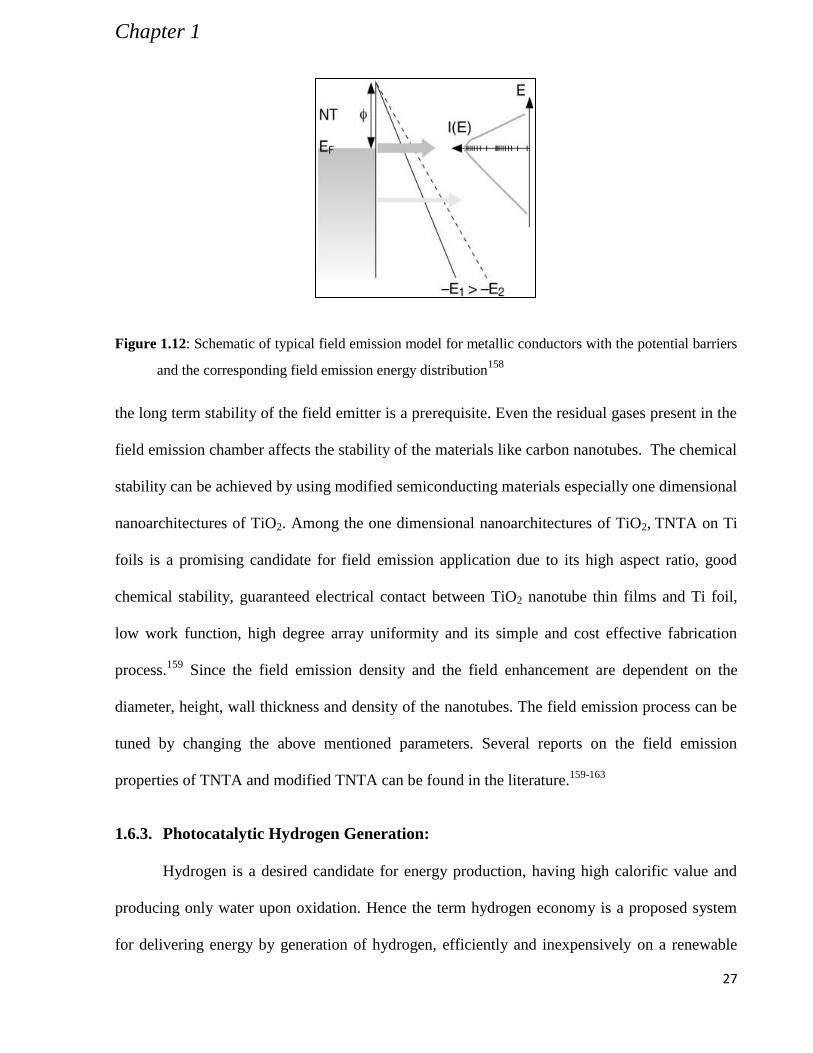
Chapter 1
27
Figure 1.12: Schematic of typical field emission model for metallic conductors with the potential barriers
and the corresponding field emission energy distribution158
the long term stability of the field emitter is a prerequisite. Even the residual gases present in the
field emission chamber affects the stability of the materials like carbon nanotubes. The chemical
stability can be achieved by using modified semiconducting materials especially one dimensional
nanoarchitectures of TiO2. Among the one dimensional nanoarchitectures of TiO2, TNTA on Ti
foils is a promising candidate for field emission application due to its high aspect ratio, good
chemical stability, guaranteed electrical contact between TiO2 nanotube thin films and Ti foil,
low work function, high degree array uniformity and its simple and cost effective fabrication
process.159
Since the field emission density and the field enhancement are dependent on the
diameter, height, wall thickness and density of the nanotubes. The field emission process can be
tuned by changing the above mentioned parameters. Several reports on the field emission
properties of TNTA and modified TNTA can be found in the literature.159-163
1.6.3. Photocatalytic Hydrogen Generation:
Hydrogen is a desired candidate for energy production, having high calorific value and
producing only water upon oxidation. Hence the term hydrogen economy is a proposed system
for delivering energy by generation of hydrogen, efficiently and inexpensively on a renewable

Chapter 1
28
basis. Hydrogen generation by photocatalysis reaction employing semiconducting materials is an
efficient and cost effective route in hydrogen economy. As mentioned earlier in this chapter,
nanoarchitectures of TiO2 are appropriate for photocatalytic hydrogen production.
Water splitting into H2 and O2 is an uphill reaction. It needs the standard Gibb’s free
energy change (∆G0) of 237 kJ / mol or 1.23 V
20, as represented in equation,
(2)
Therefore, in order to achieve water splitting, the band gap of the semiconducting material
should be greater than 1.23 eV. As mentioned previously the reduction and oxidation potential of
H2O should lie within the band gap of the material (figure 1.4). Thus band gap structure of the
material is a thermodynamic requirement for photocatalytic hydrogen generation. Life time of
the photogenerated electrons, charge separation and mobility are the other factors which affect
the efficiency of photocatalytic hydrogen generation.20
The processes in the photocatalytic
hydrogen generation includes absorption of light by semiconductor, generation of charge
carriers, separation, migration and transfer of the charge carriers to water or other molecule.
Recombination of charge carriers is a competing process which reduces the hydrogen generation
efficiency9. Any other processes which consume the excited electrons should be avoided to
increase the efficiency. Effective charge separation and migration is essential requirement for
efficient hydrogen generation. This can be achieved by surface modification of the
semiconducting material. As discussed earlier, noble metal (Pt) loading is a widely adopted
method for efficient charge separation and generation of active sites for hydrogen production.70
The efficient hydrogen generation due to noble metal loading is attributed to the formation of
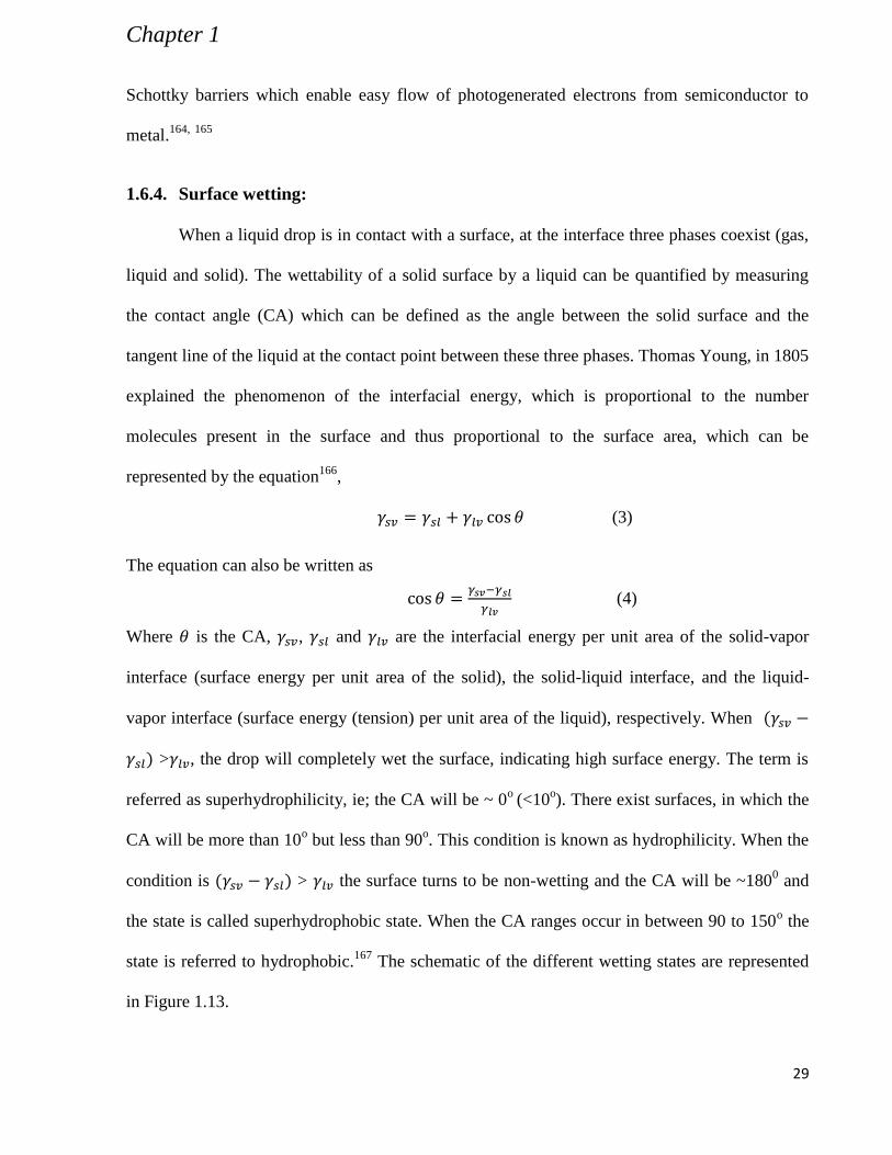
Chapter 1
29
Schottky barriers which enable easy flow of photogenerated electrons from semiconductor to
metal.164,
165
1.6.4. Surface wetting:
When a liquid drop is in contact with a surface, at the interface three phases coexist (gas,
liquid and solid). The wettability of a solid surface by a liquid can be quantified by measuring
the contact angle (CA) which can be defined as the angle between the solid surface and the
tangent line of the liquid at the contact point between these three phases. Thomas Young, in 1805
explained the phenomenon of the interfacial energy, which is proportional to the number
molecules present in the surface and thus proportional to the surface area, which can be
represented by the equation166
,
(3)
The equation can also be written as
(4)
Where is the CA, , and are the interfacial energy per unit area of the solid-vapor
interface (surface energy per unit area of the solid), the solid-liquid interface, and the liquid-
vapor interface (surface energy (tension) per unit area of the liquid), respectively. When
> , the drop will completely wet the surface, indicating high surface energy. The term is
referred as superhydrophilicity, ie; the CA will be ~ 0o
(<10o). There exist surfaces, in which the
CA will be more than 10o but less than 90
o. This condition is known as hydrophilicity. When the
condition is > the surface turns to be non-wetting and the CA will be ~1800 and
the state is called superhydrophobic state. When the CA ranges occur in between 90 to 150o the
state is referred to hydrophobic.167
The schematic of the different wetting states are represented
in Figure 1.13.

Chapter 1
30
Figure 1.13: Different wetting states derived on the basis of Young’s equation
The Young’s equation is valid only for smooth surfaces. When the surface roughness and
chemical nature comes into picture, the non ideal behavior can be observed and two extreme
cases can happen, ie; either total wetting or non-wetting. The correlation of the surface roughness
with the former case has been derived by Wenzel168
and the latter by Cassie and Baxter169
. The
fundamental assumption in the Wenzel theory is that the liquid penetrates into the grooves of the
rough surface. He suggested a linear relationship between the observed CA and the surface
roughness
(5)
Where and are the observed (apparent) and actual CA (on a smooth surface) and r is the
surface roughness or else the ratio between the actual surface area and the geometrical surface
area. If the CA on a smooth surface is smaller than 90o, then the apparent CA on the
corresponding rough surface will be smaller than 90o and vice versa. But the theory shows
violation, by showing hydrophobicity, when large fraction of air is present in the pores of the
material. In the Cassie Baxter model, the apparent CA is be given as follows,
(6)

Chapter 1
31
Where and are the area fractions of the solid and vapor on the surface, respectively. Since
and , the equation can be written as
(7)
Figure 1.14 shows the schematic representation of the surface liquid interaction in Wenzel and
Cassie Baxter models. Wettability on the surface here is regulated by the fraction of air trapped
on the rough surface. When tend towards ‘1’ the surface becomes superhydrophobic. Thus the
wettability of the surface can be adjusted by tuning the surface roughness of the material.
Figure 1.14: Schematic representation of Wenzel and Cassie Baxter model of surface wetting due to
surface roughness.
Photoinduced changes of the chemical states on the surface can cause changes in the
wetting behaviour of the material and this makes it possible to create an intelligent surface with
controllable wettability. Superhydrophilicity is an important property that can endow materials
with self cleaning property. Among the various semiconductors, TiO2 is one of the most
important candidate material, which exhibit this phenomenon under light irradiation.170
Because
of this unique phenomenon, TiO2 is a promising candidate for self cleaning and antifogging-
coating applications.
Chapter 1
32
1.7. Objective of the thesis
The research programme pertaining to this thesis is targeted towards, synthesis and
characterization of one dimensional nanoarchitectures of pristine and doped TiO2 as well as to
study their properties pertaining to selected applications in energy, environment and electronics.
Among the various one dimensional nanostructures viz nanotubes, nanobelts, nanorods,
nanowires and fibers, nanotubes are of importance because of their high active surface area and
electron transport properties. The TiO2 nanotubular architectures considered in the present study
are vertically aligned nanotube arrays in thin film form and nanotube powders. These structures
are in general synthesized by various techniques viz hydrothermal, template assisted sol-gel,
template assisted PVD and CVD, electrospinning and electrochemical techniques. Among these,
electrochemical anodization is the most cost effective, easy to adopt (for large scale production)
and environmentally friendly. In addition, the technique provides accurate method for tuning the
aspect ratio and surface morphology of the nanotubes as these can be modified by controlling the
applied potential which in turn can be controlled accurately in nanovolt levels.
An important drawback of TiO2 for selected applications is that its band gap is rather large, 3.0–
3.2 eV, and thus only 5% of the solar spectrum (λ < 380 nm, corresponding to the UV region) is
absorbed. To extend the photo-absorption into the visible region, doping with cations and anions
are adopted. Among the various dopants, nitrogen is found to be more promising. Hence, it is of
paramount importance to synthesize N-doped TiO2 nanotubular arrays for enhancing the
efficiency of the devices based on their architectures.
The application studies were chosen based on the enhanced properties of pristine and N-
doped TiO2 nanotube arrays and powders which are expected to improve the efficiency of
devices when fabricated using them. The specific objectives, for which present thesis work was
undertaken, are the following,

Chapter 1
33
Synthesis of pristine and N-doped vertically aligned TiO2 nanotube arrays in thin film form
by electrochemical anodization technique and their morphological, structural,
compositional and optical characterization. Delineation of dopant nature (interstitial or
substitutional in TiO2) by XPS and determination of change in electronic band gap and
interband defect states by UV-vis and photoluminescence spectroscopies were part of the
objective.
Fabrication of dye sensitized solar cells (DSSC) using vertically aligned TiO2 nanotube
arrays and their I-V characteristic studies, and field emission and wetting characteristics of
pristine and N-doped TiO2 nanotube arrays. The rationale behind choosing application
studies pertaining to DSSCs and field emission is that the alignment, high aspect ratio, thin
edges and directional electron transport properties of vertically aligned TiO2 nanotube
arrays are expected to play a major role in enhancing the efficiency of the respective
devices fabricated using them. Another important recently proposed application of
vertically aligned TiO2 nanotube arrays on Ti is controlled drug release because of its
expected hydrophobic nature due to the presence of long air trapped columns. Since it is
possible to fabricate vertically aligned TiO2 nanotube arrays of varying tube diameter and
length by changing applied potential as well as duration of anodization one can expect
preparation of samples of varying hydrophobicity. The hydrophobic surfaces can be made
superhydrophilic by photo irradiation and the same can be reverted back to initial
hydrophobic state by keeping it in dark. Hence, it is possible to make controlled drug
delivery systems by loading the vertically aligned TiO2 nanotube arrays with appropriate
drug after making it hydrophilic by light irradiation and then reverting it back to
hydrophobic state by keeping in the dark. The same can then be used in orthopedic
implants for controlled drug delivery. However, care should be taken not to expose the

Chapter 1
34
implant to light before implantation as it could become hydrophilic leading to uncontrolled
drug release. With this application in mind the studies on kinetics of hydrophobic ↔
superhydrophilic transitions were considered.
Synthesis and characterization of pristine and N-doped TiO2 nanotube powders using rapid
break down (RBA) anodization technique. The study was undertaken because in certain
applications like hydrogen generation by photolysis of water, destruction of organics and
microbes in water, nanotubes in powder form are advantageous as they can be suspended in
the media to yield uniform dispersion thereby facilitating better light harvesting with better
kinetics.
Investigations on hydrogen generation efficiency of platinum loaded TiO2 nanotube
powders from ethanol/water mixtures under different wavelength photo irradiation as well
as dye degradation kinetics using pristine and doped TiO2 nanotube powders.

Chapter 1
35
References
1 Banerjee, A. N., Nanotech. Sci. App. 2011, 4, 35-65
2 Weir, A.; Westerhoff, P.; Fabricius, L.; Hristovski, K.; von Goetz, N., Environ. Sci. Technol. 2012, 46 (4), 2242-
2250.
3 Clark, W.; Broadhead, P., J. Phys. C: Solid St. Phys 1970, 3 (5), 1047.
4 Layman, P., Chemical & Engineering News Archive 1996, 74 (4), 13-14.
5 Harris, A. W.; Ludden, B. P.; Blaikley, D. C. W., Vacuum 1992, 43 (1–2), 143-147.
6 Frank, S. N.; Bard, A. J., J. Am. Chem. Soc 1977, 99 (1), 303-304.
7 Ohko, Y.; Hashimoto, K.; Fujishima, A., J. Phys. Chem A 1997, 101 (43), 8057-8062.
8 Sakata, T.; Kawai, T., Chem. Phys. Lett. 1981, 80 (2), 341-344.
9 Linsebigler, A. L.; Lu, G.; Yates, J. T., Chem. Rev. 1995, 95 (3), 735-758.
10 Brian O'Regan & Michael Gratzel, Nature, 1991, 353, 737-740
11 Gratzel, M.; Kalyanasundaram, K., Curr. Sci. 1994, 66, 706-714
12 Bonhote, P.; Moser, J. E.; Vlachopoulos, N.; Walder, L.; Zakeeruddin, S. M.; Humphry-Baker, R.; Pechy, P.;
Gratzel, M., Chem.Comm. 1996, (10), 1163-1164.
13 Wang, R.; Hashimoto, K.; Fujishima, A.; Chikuni, M,; Kojima, E.; Kitamura, A.; Shimohigoshi, M.; and
Watanabe, T., Nature, 1997, 388, 431-432
14 Al-Homoudi, I. A.; Thakur, J. S.; Naik, R.; Auner, G. W.; Newaz, G., App. Surf. Sci. 2007, 253 (21), 8607-8614.
15 Mor, G. K.; Carvalho, M. A.; Varghese, O. K.; Pishko, M. V.; Grimes, C. A., J. Mater. Res. 2004, 19 (02), 628-
634.
16 Bally, A. R.; Prasad, K.; Sanjinés, R.; Schmid, P. E.; Lévy, F.; Benoit, J.; Barthou, C.; Benalloul, P., MRS Online
Proceedings Library 1996, 424, 471-475.
17 Nishikiori, H.; Qian, W.; El-Sayed, M. A.; Tanaka, N.; Fujii, T., J. Phys. Chem. C 2007, 111 (26), 9008-9011.
18 Kondo, J. N.; Domen, K., Chem. Mater. 2007, 20 (3), 835-847.
19 Diebold, U., Surf. Sci. Rep. 2003, 48 (5–8), 53-229.
20 Chen, X.; Mao, S. S., Chem. Rev. 2007, 107 (7), 2891-2959.
21 Fujishima, A.; Zhang, X.; Tryk, D. A., Surf. Sci. Rep. 2008, 63 (12), 515-582.
22 Patzke, G. R.; Krumeich, F.; Nesper, R., Ang. Chem. Int. Ed. 2002, 41 (14), 2446-2461.
23 Tang, H.; Prasad, K.; Sanjinés, R.; Lévy, F., Sens. Act. B: Chem 1995, 26 (1–3), 71-75.
24 Brus, L. E., The Journal of Chemical Physics 1984, 80 (9), 4403-4409.
25 Efros, A. I. L., Efros, A. L. Sov. Phys. Semicond. 1982, 16, 772- 775.
26 Enright, B.; Fitzmaurice, D., J. Phys. Chem. 1996, 100 (3), 1027-1035.
27 Nozik, A. J.; Memming, R., J. Phys. Chem. 1996, 100 (31), 13061-13078.
28 Grela, M. A.; Brusa, M. A.; Colussi, A. J., J. Phys. Chem. B 1997, 101 (51), 10986-10989.

Chapter 1
36
29
Zhou, W.; Liu, H.; Boughton, R. I.; Du, G.; Lin, J.; Wang, J.; Liu, D., Journal of Materials Chemistry 2010, 20
(29), 5993-6008.
30 Tsai, C.-C.; Teng, H., Chem. Mater. 2005, 18 (2), 367-373.
31 Wang, J.; Tafen, D. N.; Lewis, J. P.; Hong, Z.; Manivannan, A.; Zhi, M.; Li, M.; Wu, N., J.Am. Chem. Soc. 2009,
131 (34), 12290-12297.
32 Joo, J.; Kwon, S. G.; Yu, T.; Cho, M.; Lee, J.; Yoon, J.; Hyeon, T., J. Phys. Chem. B 2005, 109 (32), 15297-
15302.
33 Lin, Y.; Wu, G. S.; Yuan, X. Y.; Xie, T.; Zhang, L. D., . Phys.: Condesns. Mat. 2003, 15 (17), 2917.
34 Joo, J.; Kwon, S. G.; Yu, T.; Cho, M.; Lee, J.; Yoon, J.; Hyeon, T., J. Phys. Chem. B 2005, 109 (32), 15297-
15302.
35 Burda, C.; Chen, X.; Narayanan, R.; El-Sayed, M. A., Chem. Rev. 2005, 105 (4), 1025-1102.
36 Tsai, C.-C.; Teng, H., Chem. Mater. 2004, 16 (22), 4352-4358.
37 Riss, A.; Elser, M. J.; Bernardi, J.; Diwald, O., J. Am. Chem.l Soc. 2009, 131 (17), 6198-6206.
38 Xia, Y.; Yang, P.; Sun, Y.; Wu, Y.; Mayers, B.; Gates, B.; Yin, Y.; Kim, F.; Yan, H., Adv. Mater. 2003, 15 (5),
353-389.
39 Adachi, M.; Murata, Y.; Harada, M.; Yoshikawa, S., Chem. Lett. 2000, 29 (8), 942-943.
40 Quan, X.; Yang, S.; Ruan, X.; Zhao, H., Env. Sci. Tech. 2005, 39 (10), 3770-3775.
41 Uchida, S.; Chiba, R.; Tomiha, M.; Masaki, N.; Shirai, M., Electrochemistry, 2002, 70, 418-420.
42 Adachi, M.; Okada, I.; Ngamsinlapasathian, S.; Murata, Y.; Yoshikawa, S., Electrochemistry, 2002, 70, 449-452.
43 Hasiguti, R. R., Ann. Rev. Mater. Sci. 1972, 2 (1), 69-92.
44 Cronemeyer, D. C., E, Phys. Rev. 1952, 87 (5), 876-886.
45 Wycoff, R. W. G. The Structure of Crystals; The Chemical Catalog Company Inc.: New York, 1931
46 Landmann, M.; Rauls, E.; Schmidt, W. G., J. Phys: Conden. Matt. 2012, 24 (19), 195503.
47 Henrich, V. E., Rep. Prog. Phys. 1985, 48 (11), 1481.
48 Thiên-Nga, L.; Paxton, A. T., Phys. Rev. B 1998, 58 (19), 13233-13241.
49 Landmann, M.; Rauls, E.; Schmidt, W. G., J. Phys: Condens. Mattter. 2012, 24 (19), 195503.
50 Navrotsky, A.; Jamieson, J. C.; Kleppa, O. J., Science 1967, 158 (3799), 388-389.
51 Jamieson, J.C.; Olinger, B.; Am Min. 1969, 54,1447.
52 Dabler, A.; Feltz, A.; Jung, J.; Ludwig, W.; Kaisersberger, E., J. Therm. Anal. Cal. 1988, 33 (3), 803-809.
53 Hanaor, D. H.; Sorrell, C., J Mater Sci 2011, 46 (4), 855-874.
54 Horn, M.; Schwerdtfeger, C. F.; and Meagher, E. P.; Z. Kristallogr, 1972, 136, 273-281
55 Carp, O.; Huisman, C. L.; Reller, A., Prog. Sol. St. Chem. 2004, 32 (1–2), 33-177.
56 Asahi, R.; Taga, Y.; Mannstadt, W.; Freeman, A. J. Phys. ReV. B 2000, 61, 7459.
57 Wu, Z. Y.; Ouvrared, G.; Gressier, P.; Natoli, C. R. Phys. ReV. B1997, 55, 10382.
58 Brydson, R.; Sauer, H.; Engel, W.; Thomas, J. M.; Zeitler, E.; Kosugi,N.; Kuroda, H. J. Phys.: Condens. Matter
1989, 1, 797.

Chapter 1
37
59
Brydson, R.; Williams, B. G.; Engel, W.; Sauer, H.; Zeitler, E.;Thomas, J. M. Sol. St. Commun. 1987, 64, 609.
60 Choi, H. C.; Ahn, H. J.; Jung, Y. M.; Lee, M. K.; Shin, H. J.; Kim,S. B.; Sung, Y. E. Appl. Spectrosc. 2004, 58,
598.
61 Balachandran, U.; Eror, N. G., J Mater Sci 1988, 23 (8), 2676-2682.
62 Sekiya, T.; Ichimura, K.; Igarashi, M.; Kurita, S., J. Phys. Chem. Sol. 2000, 61 (8), 1237-1242.
63 Hasiguti, R. R.; Yagi, E., Phys. Rev. B 1994, 49 (11), 7251-7256.
64 Herrmann, J.-M., Cat. Today 1999, 53 (1), 115-129.
65 Nosaka, Y.; Fox, M. A., J. Phys. Chem. 1988, 92 (7), 1893-1897.
66 Ni, M.; Leung, M. K. H.; Leung, D. Y. C.; Sumathy, K., Renew. Sust. Ener. Rev. 2007, 11 (3), 401-425.
67 (a) Munter, R., , Proc. Estonian Acad. Sci. Chem. 2001,50, 59-80, 2001; (b) CRC Handbook, 1985.(c)Dean, J.
A.; Lange’s Handbook of Chemistry, 11ed, New York, McGraw-
Hill 1973.(d) Gratzel,M. Heterogeneous Electron Transfer; CRC Press: Boca Raton, FL, 1989 (e) Hoffmann, M. R.;
Martin, S. T.; Choi, W.; Bahnemann, D. W., Chem. Rev. 1995, 95 (1), 69-96. 68
Fujishima, A.; Honda, K., Nature, 1972, 238, 37-38.
69 Wu, G.; Chen, T.; Zhou, G.; Zong, X.; Li, C., Sci. Chin. B: Chem. 2008, 51 (2), 97-100.
70 Sato, S.; White, J. M., Chem. Phys. Lett. 1980, 72 (1), 83-86.
71 Idakiev, V.; Yuan, Z. Y.; Tabakova, T.; Su, B. L., App. Catal.s A: General 2005, 281 (1–2), 149-155.
72 Gerischer, H.; Willig, F.; Meier, H.; Jahnke, H.; Schönborn, M.; Zimmermann, G., Eds. Springer Berlin /
Heidelberg: 1976; Vol. 61, pp 31-84.
73 Vlachopoulos, N.; Liska, P.; Augustynski, J.; Graetzel, M., J. Am. Chem. Soc. 1988, 110 (4), 1216-1220.
74 Kamat, P. V.; Fox, M. A., Chem. Phys. Lett. 1983, 102 (4), 379-384.
75 Desilvestro, J.; Graetzel, M.; Kavan, L.; Moser, J.; Augustynski, J., J. Am. Chem. Soc. 1985, 107 (10), 2988-2990.
76 Peng, T.; Dai, K.; Yi, H.; Ke, D.; Cai, P.; Zan, L., Chem. Phy. Lett. 2008, 460 (1–3), 216-219.
77 Jang, J. S.; Li, W.; Oh, S. H.; Lee, J. S., Chem. Phys. Lett. 2006, 425 (4–6), 278-282.
78 Sasikala, R.; Shirole, A.; Sudarsan, V.; Sakuntala, T.; Sudakar, C.; Naik, R.; Bharadwaj, S. R., Int. J. Hyd. Ener.
2009, 34 (9), 3621-3630.
79 Hirai, T.; Suzuki, K.; Komasawa, I., J. Coll. Inter. Sci. 2001, 244 (2), 262-265.
80 Kato, H.; Kudo, A., J. Phys. Chem. B 2002, 106 (19), 5029-5034.
81 Liu, J. W.; Chen, G.; Li, Z. H.; Zhang, Z. G., J. Solid. Stat. Chem. 2006, 179 (12), 3704-3708.
82 Hwang, D. W.; Kim, H. G.; Lee, J. S.; Kim, J.; Li, W.; Oh, S. H., J. Phys. Chem. B 2004, 109 (6), 2093-2102.
83 Borgarello, E.; Kiwi, J.; Graetzel, M.; Pelizzetti, E.; Visca, M., J. Am. Chem. Soc. 1982, 104 (11), 2996-3002.
84 Lindgren, T.; Mwabora, J. M.; Avendaño, E.; Jonsson, J.; Hoel, A.; Granqvist, C.-G.; Lindquist, S.-E., J. Phys.
Chem. B 2003, 107 (24), 5709-5716.
85 Chen, X.; Burda, C., J. Am. Chem. Soc. 2008, 130 (15), 5018-5019.
86 Ohno, T.; Mitsui, T.; Matsumura, M., Chem. Lett. 2003, 32 (4), 364-365.
87 Le Paven-Thivet, C.; Ishikawa, A.; Ziani, A.; Le Gendre, L.; Yoshida, M.; Kubota, J.; Tessier, F.; Domen, K., J.
Phys. Chem. C 2009, 113 (15), 6156-6162.

Chapter 1
38
88
Sant, P. A.; Kamat, P. V., Phys. Chem. Chem. Phys. 2002, 4 (2), 198-203.
89 Baker, D. R.; Kamat, P. V., Adv. Func. Mater. 2009, 19 (5), 805-811.
90 Evans, J. E.; Springer, K. W.; Zhang, J. Z., J. Chem. Phys.s 1994, 101 (7), 6222-6225.
91 Yao, Y.; Li, G.; Ciston, S.; Lueptow, R. M.; Gray, K. A., Env. Sci. Tech. 2008, 42 (13), 4952-4957.
92 Choi, W.; Termin, A.; Hoffmann, M. R., J. Phys. Chem. 1994, 98 (51), 13669-13679.
93 Asahi, R.; Morikawa, T.; Ohwaki, T.; Aoki, K.; Taga, Y., Science 2001, 293 (5528), 269-271.
94 Chen, X.; Lou, Y. B.; Samia, A. C. S.; Burda, C.; Gole, J. L., Adv. Func. Mater. 2005, 15 (1), 41-49.
95 Nakamura, R.; Tanaka, T.; Nakato, Y., J. Phys. Chem. B 2004, 108 (30), 10617-10620.
96 Di Valentin, C.; Finazzi, E.; Pacchioni, G.; Selloni, A.; Livraghi, S.; Paganini, M. C.; Giamello, E., Chem. Phys.
2007, 339 (1–3), 44-56.
97 Diwald, O.; Thompson, T. L.; Goralski, E. G.; Walck, S. D.; Yates, J. T., J. Phys.Chem. B 2003, 108 (1), 52-57.
98 Chen, X.; Burda, C., J. Phys. Chem. B 2004, 108 (40), 15446-15449.
99 Di Valentin, C.; Pacchioni, G.; Selloni, A.; Livraghi, S.; Giamello, E., J. Phys. Chem. B 2005, 109 (23), 11414-
11419.
100 Di Valentin, C.; Pacchioni, G.; Selloni, A., Phys. Rev. B 2004, 70 (8), 085116.
101 Miyauchi, M.; Ikezawa, A.; Tobimatsu, H.; Irie, H.; Hashimoto, K., Phys. Chem. Chem. Phys. 2004, 6 (4), 865-
870.
102 Thompson, T. L.; Yates, J. T., Chem. Rev. 2006, 106 (10), 4428-4453.
103 Dunnill, C. W.; Parkin, I. P., Dalt. Trans. 2011, 40 (8), 1635-1640.
104 Kasuga, T.; Hiramatsu, M.; Hoson, A.; Sekino, T.; Niihara, K., Langmuir 1998, 14 (12), 3160-3163.
105 Zhu, Y.; Li, H.; Koltypin, Y.; Hacohen, Y. R.; Gedanken, A., Chem. Comm. 2001, (24), 2616-2617.
106 Kasuga, T.; Hiramatsu, M.; Hoson, A.; Sekino, T.; Niihara, K., Adv. Mater. 1999, 11 (15), 1307-1311.
107 Jung, J. H.; Kobayashi, H.; van Bommel, K. J. C.; Shinkai, S.; Shimizu, T., Chem. Mater. 2002, 14, 1445-1447.
108 Zhang, Q.; Gao, L., Langmuir 2002, 19 (3), 967-971.
109 Feng, X.; Shankar, K.; Varghese, O. K.; Paulose, M.; Latempa, T. J.; Grimes, C. A., Nano Lett. 2008, 8 (11),
3781-3786.
110 Feng, X.; Zhai, J.; Jiang, L., Ang. Chem. Int. Ed. 2005, 44 (32), 5115-5118.
111 Pradhan, S. K.; Reucroft, P. J.; Yang, F.; Dozier, A., J. Cryst. Growth 2003, 256 (1–2), 83-88.
112 Wu, J.-J.; Yu, C.-C., J. Phys. Chem. B 2004, 108 (11), 3377-3379.
113 Wu, J.-M.; Shih, H. C.; Wu, W.-T.; Tseng, Y.-K.; Chen, I. C., J. Cryst. Growth 2005, 281 (2–4), 384-390.
114 Lei, Y.; Zhang, L. D.; Fan, J. C., Chem. Phys. Letters 2001, 338 (4–6), 231-236.
115 Liu, S.; Huang, K., Sol. Ener. Mater. Solar Cells 2005, 85 (1), 125-131.
116 Gong, D.; Grimes, C. A.; Varghese, O. K.; Hu, W.; Singh, R. S.; Chen, Z.; Dickey, E. C., J. Mater. Res. 2001, 16
(12), 3331-3334.
117 Bessekhouad, Y.; Robert, D.; Weber, J. V., J. Photochem. Photobio. A: Chem. 2003, 157 (1), 47-53.

Chapter 1
39
118
Chen, Y.; Crittenden, J. C.; Hackney, S.; Sutter, L.; Hand, D. W., Environ. Sci. Tech. 2005, 39 (5), 1201-1208.
119 Jung, J. H.; Kobayashi, H.; van Bommel, K. J. C.; Shinkai, S.; Shimizu, T., Chem. Mater. 2002, 14 (4), 1445-
1447.
120 Wang, W.; Varghese, O. K.; Paulose, M.; Grimes, C. A.; Wang, Q.; Dickey, E. C., J. Mater. Res. 2004, 19 (02),
417-422.
121 Yao, B. D.; Chan, Y. F.; Zhang, X. Y.; Zhang, W. F.; Yang, Z. Y.; Wang, N., App. Phys. Lett. 2003, 82 (2), 281-
283.
122 Masuda, H.; Fukuda, K., Science 1995, 268 (5216), 1466-1468.
123 Possin, G. E., Rev. Sci. Inst. 1970, 41 (5), 772-774.
124 AlMawlawi, D.; Coombs, N.; Moskovits, M., J. App. Phys. 1991, 70 (8), 4421-4425.
125 Kawai, S.; Ueda, R., J. Electrochem. Soc. 1975, 122 (1), 32-36.
126 McGarvey, C. E.; Holden, D. A., Langmuir 1990, 6 (6), 1123-1132.
127 Zwilling, V.; Darque-Ceretti, E.; Boutry-Forveille, A.; David, D.; Perrin, M. Y.; Aucouturier, M., Surf. Inter.
Anal. 1999, 27 (7), 629-637.
128 Grimes, C. A., J. Mater. Chem. 2007, 17 (15), 1451-1457.
129 Mor, G. K.; Varghese, O. K.; Paulose, M.; Shankar, K.; Grimes, C. A., Sol. Ener. Mater. Solar Cells 2006, 90
(14), 2011-2075.
130 Schultze, J. W.; Lohrengel, M. M., Electrochim. Acta 2000, 45 (15–16), 2499-2513.
131 Pourbaix, M. Atlas d’Equilibres Electrochimiques; GauthierVillars: Paris, 1963; pp 644.
132 Carter, V. E., Metallic Coatings for Corrosion Control, Hants (Butterworth), 1977,27.
133 Caprani, A.; Epelboin, I.; Morel, P., J. Electroanal. Chem. Interfac.Electrochem. 1973, 43 (1), A2-A9.
134 Mandry, M. J.; Rosenblatt, G., J. Electrochem. Soc. 1972, 119 (1), 29-33.
135 Kelly, J. J., Electrochim. Acta 1979, 24 (12), 1273-1282.
136 Macak, J. M.; Tsuchiya, H.; Ghicov, A.; Yasuda, K.; Hahn, R.; Bauer, S.; Schmuki, P., Curr. Op. Solid State.
Mater. Sci. 2007, 11 (1–2), 3-18.
137 Prakasam, H. E.; Shankar, K.; Paulose, M.; Varghese, O. K.; Grimes, C. A., J. Phys.Chem. C 2007, 111 (20),
7235-7241.
138 Narayanan, R.; Kwon, T.-Y.; Kim, K.-H., Mater. Lett. 2009, 63 (23), 2003-2006.
139 Mor, G. K.; Varghese, O. K.; Paulose, M.; Ong, K. G.; Grimes, C. A., Thin Solid Films 2006, 496 (1), 42-48.
140 Zhu, Y.; Li, H.; Koltypin, Y.; Hacohen, Y. R.; Gedanken, A., Chem. Comm. 2001, (24), 2616-2617.
141 Cai, Q.; Paulose, M.; Varghese, O. K.; Grimes, C. A., J. Mater. Res. 2005, 20 (01), 230-236.
142 Prakasam, H. E.; Shankar, K.; Paulose, M.; Varghese, O. K.; Grimes, C. A., J. Phys. Chem. C 2007, 111 (20),
7235-7241.
143 Paulose, M.; Shankar, K.; Yoriya, S.; Prakasam, H. E.; Varghese, O. K.; Mor, G. K.; Latempa, T. A.; Fitzgerald,
A.; Grimes, C. A., J. Phys. Chem. B 2006, 110 (33), 16179-16184.
144 Mor, G. K.; Prakasam, H. E.; Varghese, O. K.; Shankar K.; Grimes, C. A., Nano. Lett., 2007, 7, 2356-2364.

Chapter 1
40
145
Macak, J. M.; Tsuchiya, H.; Berger, S.; Bauer, S.; Fujimoto S.; Schmuki, P., Chem. Phys. Lett., 2006,,428, 421-
425.
146 Varghese, O. K.; Paulose, M.; Grimes, C. A., Nat. Nano 2009, 4 (9), 592-597.
147 O'Regan, B, Grätzel, M., Nature,1991, 353, 737-740.
148 Robertson, N., Angew. Chem. Int. Ed. 2006, 45 (15), 2338-2345.
149 Mishra, A.; Fischer, M. K. R.; Bäuerle, P., Angew. Chem. Int. Ed. 2009, 48 (14), 2474-2499.
150 Oskam, G.; Bergeron, B. V.; Meyer, G. J.; Searson, P. C., J. Phys. Chem. B 2001, 105 (29), 6867-6873.
151 Nusbaumer, H.; Moser, J.-E.; Zakeeruddin, S. M.; Nazeeruddin, M. K.; Grätzel, M., J. Phys. Chem. B 2001, 105
(43), 10461-10464.
152 Huang, S. Y.; Schlichthörl, G.; Nozik, A. J.; Grätzel, M.; Frank, A. J., J. Phys.Chem. B 1997, 101 (14), 2576-
2582.
153 Boschloo, G.; Hagfeldt, A., Acc. Chem. Res. 2009, 42 (11), 1819-1826.
154 Zhang, Z.; Chen, P.; Murakami, T. N.; Zakeeruddin, S. M.; Grätzel, M., Adv. Func. Mater. 2008, 18 (2), 341-
346.
155 Wang, M.; Chamberland, N.; Breau, L.; Moser, J.; Baker, R. H.; Marsan, B.; Zakeeruddin, S. M.; Gratzel, M.,
Nat. Chem, 2010, 2, 385- 389.
156 Roy, P.; Kim, D.; Lee, K.; Spiecker, E.; Schmuki, P., Nanoscale 2010, 2 (1), 45-59.
157 Ghicov, A.; Albu, S. P.; Hahn, R.; Kim, D.; Stergiopoulos, T.; Kunze, J.; Schiller, C.-A.; Falaras, P.; Schmuki,
P., Chemistry – An Asian Journal 2009, 4 (4), 520-525.
158 Bonard, J. M.; Kind, H.; Stockli, T.; Nilsson, L. O., Solid State Electron. 2001, 45 (6), 893-914.
159 Yahya, A.; Michael, K.; Sabee, M., Nanotechnol. 2010, 21 (50), 505706.
160 Miyauchi, M.; Tokudome, H.; Toda, Y.; Kamiya, T.; Hosono, H., App. Phys. Lett. 2006, 89 (4), 043114-3.
161 Alivov, Y.; Klopfer, M.; Molloi, S., App. Phys. Lett 2010, 96 (24), 243502-3.
162 Kang, Y.-M.; Wang, C.-W.; Chen, J.-B.; Wang, L.-Q.; Li, D.-S.; Zhu, W.-D.; Zhou, F., J. Vac. Sci. Tech. B.
2012, 30 (4), 041801.
163 Wang, L.-Q.; Wang, C.-W.; Chen, J.-B.; Guo, R.-S.; Zhou, F.; Liu, W.-M., Thin Solid Films 2011, 519 (22),
8173-8177.
164 Korzhak, A. V.; Ermokhina, N. I.; Stroyuk, A. L.; Bukhtiyarov, V. K.; Raevskaya, A. E.; Litvin, V. I.; Kuchmiy,
S. Y.; Ilyin, V. G.; Manorik, P. A., J. Photochem. Photobio. A, 2008, 198 (2–3), 126-134.
165 Gurunathan, K., Int. J. Hydrogen Energy. 2004, 29 (9), 933-940.
166 Young, T., Phil. Trans. R. Soc. Lond, 1805, 95, 65.
167 Drelich, J.; Chibowski, E., Langmuir 2010, 26 (24), 18621-18623.
168 Wenzel, R. N., Ind. Eng. Chem. 1936, 28 (8), 988-994.
169 Cassie, A. B. D.; Baxter, S., Trans. Faraday Soc. 1944, 40, 546-551.
170 Wang, R.; Hashimoto, K.; Fujishima, A.; Chikuni, M.; Kojima, E.; Kitamura, A.; Shimohigoshi, M.; Watanabe,
T., Nature 1997, 388 (6641), 431-432.

Chapter 2
41
Chapter 2
Experimental Techniques
The chapter provides a brief description of the experimental techniques used for the
synthesis, characterization and studies pertaining to application of pristine and doped TiO2
nanotube arrays (TNTA) and powders. The synthesis of the pristine and doped nanotube arrays
and powders were carried out using an in-house built electrochemical anodization facility whose
details are explained. Following the details of anodization facility, the basic principles of
electron microscopic techniques, Scanning Electron Microscopy (SEM) and Transmission
Electron Microscopy (TEM), used for the morphological characterization of the synthesized
samples are discussed. This is followed by discussion of the techniques used for structural
characterization (X-Ray Diffraction (XRD) in powder and glancing incidence modes, and Raman
spectroscopy) and compositional analyses (X-ray Photoelectron Spectroscopy (XPS)). The basic
principles of Photoluminescence (PL) and Ultra violet-visible absorption spectroscopy (UV-Vis)
used for studying electronic energy band structure as well as to identify localized excitations or
impurities, Fourier Transform Infra Red Spectroscopy (FTIR) utilized to study physisorbed and
chemisorbed surface species, Brunauer, Emmett and Teller (BET) and Temperature
Programmed Desorption Reduction and Oxidation (TPDRO) methods used for physisorption and
chemisorption surface area measurements are also discussed. Further, the details of the
experimental facilities used to carry out studies pertaining to selected applications are outlined.

Chapter 2
42
2.1. Anodization Facility
The schematic of the experimental setup used for anodization is shown in Figure 2.1.
Prior to the electrochemical anodization, the Ti foils (10 mm X 10 mm) were cleaned
ultrasonically and washed sequentially with distilled water, ethanol and acetone. A two electrode
configuration consisting of Ti anode and Pt counter electrode was employed. A programmable
DC power supply (Agilent N5700A) and a multimeter (Agilent 34401A) interfaced to a PC were
used for DC voltage supply and measurement of current transients respectively. All anodization
reactions were performed under potentiostatic conditions in fluoride or chloride ion containing
medium. After anodization, the samples were sequentially sonicated in distilled water, ethanol
and acetone, followed by drying in N2 gas stream.
Figure 2.1: Schematic of the potentiostatic anodization set up
2.2. Electron Microscopy
Electron microscopy is a field of science in which electron beam is used to form a
magnified image as well as yield diffraction pattern corresponding to the material under

Chapter 2
43
inspection. It takes advantage of much shorter wavelength of the electrons and focusing is done
through electromagnetic lenses. Electrons accelerated onto a material result in a number of
interactions with the atoms of the target sample. Accelerated electrons can pass through the
sample without interaction; undergo elastic as well as inelastic scattering thereby resulting in a
number of signals that are used for imaging, quantitative and semi-quantitative analyses as well
as structure elucidation. The schematic of the processes taking place because of material-electron
interaction are depicted in Figure 2.2.
Figure 2.2: Schematic of processes taking place during electron - material interaction.
2.2.1. Scanning Electron Microscopy
Scanning electron microscopy (SEM) is a versatile tool used for surface characterization
of materials. The SEM provides the investigator with a highly magnified image of the material
surface that is very similar to what one would expect if one could actually "see" the surface
visually. The resolution of the SEM can approach a few nm and it can operate at magnifications
that are easily adjusted from about 10x to 300,000x. In the SEM, a source of high energy
electrons (primary electrons) is focused (in vacuum) into a fine probe that is rastered over the

Chapter 2
44
surface of the specimen. When the high-energy primary electron interacts with an atom, it
undergoes either inelastic scattering with atomic electrons or elastic scattering with the atomic
nucleus. This results in secondary electrons (used to produce SEM images), back scattered
electrons (used for illustrating contrasts in composition in multiphase samples), diffracted back
scattered electrons (used to determine crystal structure and orientation), X-ray photons (used for
elemental analysis), visible light and heat. The technique is considered to be non destructive
except for the fact that often electron beams can bring about radiation induced surface damage.
During inelastic collision with an electron, some amount of energy is transferred to the
electron of the target atom. If the energy transfer is very small, the electron emitted from the
atom will probably not have enough energy to exit the surface. If the energy transferred exceeds
the work function of the material, the emitted electron can exit the solid surface and are termed
as secondary electrons (SE). The energy of these emitted electrons is less than ~50 eV. Most of
the emitted SEs are produced within the first few nm of the surface. Secondary electrons
produced much deeper in the material suffer additional inelastic collisions, which lower their
energy and generally get trapped in the interior of the solid. A fraction of the primary electrons
which have undergone elastic scattering with the atomic nucleus (without loss of KE) are back
scattered. These backscattered electrons (BSEs) have energies comparable to the primary
electron beam. When the energy of the emitted electron is greater than 50 eV, by convention, it is
referred as BSE. In SEM equipment, the electrons coming out from the specimen surface (SEs
and BSEs) are collected by appropriate detectors. The output from the detector is used to
modulate the brightness of a cathode ray tube (CRT) whose X- and Y- inputs are driven in
synchronism with the X-Y voltages rastering the electron beam. In this way, an image is
produced on the CRT. Every point that is struck by the beam on the sample surface is mapped

Chapter 2
45
directly onto a corresponding point on the screen. The secondary electrons are the most common
signal used in the SEM and have multiple applications e.g. morphological analysis, particles size
measurements, fracture analysis, microstructural homogeneity and determination of coating
thickness.1
In addition to secondary electrons imaging, Energy Dispersive X-ray (EDX) analysis is
also a useful tool which is widely used for chemical analysis. The collision of primary electrons
with electrons of the atom can cause ejection of core electrons. The excited atom will decay to its
ground state by emitting either a characteristic X-ray photon or an Auger electron. The X-ray
emission signal can be sorted by energy using an energy dispersive X-ray detector or by
wavelength with a wavelength spectrometer (EPMA). These distributions are characteristic of
the elements that produced them and can be used to produce elemental images depicting spatial
distribution of particular elements in a given field of view. The detectors produce an output
signal that is proportional to the number of X-ray photons in the area under electron
bombardment. In EDX equipment the output is displayed in the form of a histogram of counts
versus X-ray energy. The characteristic X-rays emitted from the sample serve as fingerprints and
provide elemental information of the samples permitting semi-quantitative analysis, quantitative
analysis, line profiling and spatial distribution imaging. SEM with X-ray analysis is an efficient,
inexpensive and non-destructive tool which has become quite essential for the day to day surface
analysis.
The essential components of an electron microscope are electron emission gun, electron
lenses, sample stage, detectors for all signals of interest, display and data acquisition devices.
This equipment also has infrastructure requirements such as power supply, vacuum system,

Chapter 2
46
cooling system, vibration free floor and it needs to be installed in a room, free of ambient
magnetic and electric fields.
In conventional SEMs, electrons are generated by heating the tungsten filament or
lanthanum hexaboride (LaB6) crystal to high temperatures (~2800oC) (thermionic field emitter).
Thermionic sources suffer from relatively low brightness, evaporation of cathode material and
thermal drift during operation, which limit electron source life time and low image resolution.
Field emission is one way of generating electrons that avoids many of these problems. A Field
Emission Source (FES), also known as a cold cathode field emitter, does not need heating of the
emitter material. The emission is achieved by placing the emitter in a huge electrical potential
gradient (0.5 to 30 KV). The FES is usually a tungsten wire fashioned into a sharp point. The
significance of the small tip radius (~ 100 to 10 nm) is that an electric field can be concentrated
to an extreme level, becoming so big that the work function of the material is lowered, enabling
easy generation of electrons. The electron beam produced by the field emission is 1000 times
narrower than that produced in a conventional SEM and produces cleaner images with much less
electrostatic distortions and high spatial resolution (< 2 nm). In contrast to a conventional
tungsten filament, an FE tip can last, theoretically, for a lifetime provided the vacuum is
maintained stable. This high spatial resolution permits one to image nanoscale topography and
ultra small scale phenomena.
Field Emission Scanning Electron Microscopes (FEG Quanta, Philips, Netherlands and
Zeiss, Germany) having EDX facilities were employed for the morphological analysis in the
present study. Semi-quantitative elemental analyses were carried out using the EDX facilities
attached to the FESEMs.

Chapter 2
47
2.2.2. Transmission Electron Microscopy
Transmission electron microscopy is an established technique for examining the crystal
structure as well as microstructure of materials. It is used to study all varieties of solid materials:
metals, ceramics, semiconductors, polymers, and composites. TEM offers two distinct methods
of specimen observation, diffraction mode and image mode.2 A schematic representation of the
general image and diffraction modes of TEM is given in Figure 2.3.
Figure 2.3. Schematic representation of general image and diffraction modes of TEM
In diffraction mode, an electron diffraction pattern originating from the sample area
illuminated by the electron beam and formed at the back focal plane of the objective lens, is
obtained on the fluorescent screen. The diffraction pattern is obtained by setting the array of
magnetic lenses beneath the specimen (post-specimen lenses) so as to examine / magnify the
information in the transmitted signal at the back focal plane of the objective lens. The diffraction
pattern is entirely equivalent to an X-ray diffraction pattern: a single crystal will produce a spot
pattern on the screen, a poly-crystal will produce a ring pattern (assuming that the illuminated

Chapter 2
48
area includes sufficient number of crystallites). A glassy or amorphous material produces a series
of diffuse halos.
In order to obtain diffraction pattern from a desired region of interest (ROI) from a given
specimen, selected area electron diffraction (SAED) is carried out. In SAED, the condenser lens
is defocused to produce parallel illumination at the specimen and a selected-area aperture is used
to limit the diffracting volume. The SAED pattern is a superposition of diffraction patterns
originating from crystallites present in an illuminated ROI that possess distinct orientations.
In the imaging mode, a magnified image of the illuminated ROI is produced in the image
plane of the objective lens. The image can contain contrast brought about by several
mechanisms: mass contrast, due to spatial separations between distinct atomic constituents;
thickness contrast, due to non-uniformity in sample thickness; diffraction contrast, which in the
case of crystalline materials results from scattering of the incident electron wave by structural
defects; and phase contrast. In the imaging mode, there are three types of operations viz. bright
field, dark field and high resolution microscopy. In bright-field microscopy, a small objective
aperture is used to block all diffracted beams and to pass only the transmitted (undiffracted)
electron beam. Whereas, for dark field microscopy all the directly transmitted beams are blocked
and only diffracted beams are let by placing the objective aperture around the diffracted beam in
the SAED pattern. In case of high-resolution TEM, transmitted beams along with at least one
diffracted beam is admitted by using a large-diameter objective diaphragm. All of the beams
passing through the objective aperture are then made to recombine in the image-forming process,
in such a way that their amplitudes and phases are preserved. When viewed at high-
magnification, it is possible to observe contrast in the image in the form of periodic fringes.
These fringes represent direct resolution of the Bragg diffracting planes. Thus this mode of

Chapter 2
49
contrast is referred to as phase contrast. The fringes that are visible in the high-resolution image
originate from those planes that are oriented as Bragg reflecting planes and possess interplanar
spacing greater than the lateral spatial resolution limits of the instrument. In addition, the highly
energetic beam of electrons used in TEM interacts with sample matter to produce characteristic
radiation and particles. From these signals information regarding composition can be extracted.
TEM (Philips, Netherlands) was employed for the morphological and structural
characterization of all the samples investigated for the present work.
2.3. X ray Diffraction
When an electromagnetic radiation of wavelength impinges on a material having
periodic structures with geometrical variations in the length scale of, diffraction effect occurs.
Since X-rays have wavelength comparable to interatomic spacing in a crystal, it can interact with
the solid and scatter to produce a diffraction pattern3. This happens when the interaction satisfies
the Braggs diffraction criterion:
(1)
where d is the inter-planar spacing (i.e. spacing between adjacent planes in a set of planes, figure
2.4), the angle of incidence, n the integer representing the order of diffraction, and the
wavelength of the X-ray (normally Cu K =1.54056 Ao). Each peak in the diffraction pattern
can be correlated to a set of planes in a crystal lattice. Different set of planes have different inter-
planar spacing and according to Bragg condition must change as d changes. A schematic view
of the X-ray Diffraction (XRD) process is shown in Figure 2.4. The X-ray Diffractometer
typically uses Bragg-Brentano geometry for recording the diffraction pattern. Generally, the

Chapter 2
50
diffraction pattern is plotted as intensity versus diffraction angle 2 . In powder XRD, the X-rays
can penetrate to a material depth in the range of 0.1 to 10 ,mm depending on the material type
and the incident X-ray energy.
Figure 2.4: Schematic representation of the X-ray diffraction process
Glancing incidence X-ray diffraction (GI-XRD) is a technique used to record the
diffraction pattern of thin films, with minimum contribution acquiring from substrate. In this
case the penetration depths of the X-rays are restricted to about 10-100 nm by keeping the angle
of incidence of X-ray at a very small value (< 5o). Since the scattering volume is small, high
brilliance X-ray sources like rotating anode and synchrotron beams lines are often used. Such
surface and subsurface crystallography need fast and efficient detectors to yield significant
counts. The crystal structure of the samples are obtained by comparing the pattern with that
given in the powder diffraction file collected and maintained by Joint Committee of Powder
Diffraction Standards (JCPDS) constituted by International Commission on Diffraction Data
(ICDD). The crystallite sizes of the samples are calculated using Scherer formula.4

Chapter 2
51
(2)
where K is a dimensionless constant having value of 0.9, λ is the wave length of the incident X-
ray radiation and θ is the diffraction angle in radians. Broadening B is calculated by taking the
full width half maximum (FWHM) of the diffraction peak corresponding to each plane in the
diffraction pattern.
In the present study, the samples were analyzed in the powder and GIXRD modes using
the X-ray diffractometers of make STOI (Germany) and Bruker D8 Discover (Germany)
respectively.
2.4. Raman Spectroscopy
Raman spectroscopy is primarily a structural characterization tool. The Raman spectrum
arises from the indirect coupling of high frequency radiation (usually visible light, but also
ultraviolet and near infrared excitation sources) with the electron clouds that constitute the
chemical bonds. Such an interaction is very sensitive to the lengths, strengths, and arrangement
of bonds in a material. Elemental chemical composition plays a minor role. A crystalline lattice
with nonzero polarization exhibit Raman activity. In the case of crystals, the spectrum responds
more to details of defects and disorder than to trace impurities and related chemical
imperfections. In addition coupled modes of lattice vibrations ie; optical phonon modes influence
the spectral appearance.
When an intense monochromatic light beam impinges on the sample, the electric field of
the incident radiation distorts the electron clouds that make up the chemical bonds in the sample,
storing some energy. As the wave passes, the field reverses and the distorted electron clouds
relax back re-radiating the stored energy. Most of the stored energy is re-radiated at the same

Chapter 2
52
frequency as that of the incident excitation source. This component is known as the Rayleigh
scattering and gives a strong central line in the scattering spectrum. However, a small portion of
the stored energy is transferred to the sample exciting the vibrational modes, resulting in weak
side bands in the spectrum at frequencies less than that of the incident beam. These are the
Raman lines. Their separation from the Rayleigh line is a direct measure of the vibrational
frequencies of the sample and is generally plotted against intensity versus the difference in wave
number between the incident beam and scattered beam.5,6
The reverse process also occurs.
Existing vibrations that have been excited by thermal processes can be annihilated by coupling
with the incident beam and can add their energies to that of the source. These appear as side
bands at higher frequencies. The Raman process that excites molecular and crystal vibrations is
called Stokes scattering; the process that annihilates existing vibrations is called anti-Stokes
scattering. The two spectra are mirror images on opposite sides of the Rayleigh line. However,
because anti-Stokes scattering depends on the existence of thermally activated vibrations, the
anti-Stokes intensities are strongly temperature dependent, whereas the Stokes intensities are
only weakly temperature dependent. For this reason, anti-Stokes scattering is rarely measured,
except for the specialized technique known as coherent anti-Stokes Raman spectroscopy. The
schematic of the Raman scattering process is given in figure 2.5.
Due to the small wave vector of the optical phonon, the phonons involved in the Raman
scattering of crystalline solids have very small momentum (from the wave vector conservation
law) compared with brillouin zone. So only the zone centered phonons participate in the Raman
scattering in a normal Raman spectra process. However there are cases where non-zero center
phonons ie; phonons originating from beyond Brillouin zone boundary can be excited as is the
case with nanostructured materials. The technique is complementary to FTIR and has same

Chapter 2
53
energy shifts as infra red absorptions. The main advantages of Raman spectroscopy are its non
destructive analysis, high information content, ability to sample through the container and
minimal interference from water, as is the case with aqueous suspensions.
Figure 2.5: Schematic of Raman scattering processes
In the present study Raman spectroscopic tool is utilized to investigate the crystallinity of
the samples using Micro Raman Spectrometer (Renishaw, UK), equipped with a confocal
microscope with an “argon ion laser” operating at 514.5nm.
2.5. X-ray Photoelectron Spectroscopy
X ray photoelectron spectroscopy is a semi-quantitative technique to determine chemical
composition of the material based on photoelectric effect. This is also known as electron
spectroscopy for chemical analysis (ESCA). Photoelectron spectroscopy has been developed by
the pioneering work of Kai Siegbahn’s group in Uppsala in the 1960’s. Siegbahn was awarded
Nobel Prize in physics in 1981 for this work. His work is the basis for the use of this technique in
chemical characterization of materials. The basic principle is that the binding energy of an
electron in a molecular orbital of the molecule will be affected by the nature of its chemical
environment (chemical shift). X-ray Photoelectron Spectroscopy (XPS) utilizes photo-ionization

Chapter 2
54
and analysis of the kinetic energy distribution of the emitted photoelectrons to study the
composition and electronic state of the surface region of a sample.7 The sample is irradiated with
soft X-rays (200-2000eV) under ultra high vacuum. The photon is absorbed by an atom or
molecule (initial state effects) leading to ejection of core shell electrons (final state effects). The
energy spectra of the ejected electrons are then determined by the beta-ray spectrometer. The
kinetic energy of the photoelectrons are given by
(3)
where K.E is the kinetic energy of the photoelectrons, h the energy of the incident photon, B.E
the binding energy of the electron and the work function of the material. The photon
absorption is fast and takes place within 10-16
s. If h is less than B.E + , no photoemission
process will be initiated. As the B.E decreases the KE energy of the photoelectron increases. The
intensity of the photoelectron emission is proportional to the intensity of photons. By analyzing
the kinetic energies of the photoelectrons, the binding energy of the photoelectrons and
corresponding energies of the electronic orbitals can be calculated. Since the energies of various
orbitals are characteristic of an element, one can identify the elements present in the material,
based on the binding energies of the emitted photo electrons. Binding energy reflects the strength
of interaction between the electrons and the nuclear charge and it contains information on the
initial and final state of the atoms. The initial state accounts for the core level binding energy
shifts and is used for obtaining chemical state information. The chemical surrounding of an atom
decides the effective charge on the core electron. With the change in the chemical surrounding,
this effective charge is altered. Thus a change in binding energy is caused. This manifests as a
chemical shift or surface core level shift and is indicative of the oxidation state of the atom. More

Chapter 2
55
the binding energy, more tightly will be the electron bound to the nucleus and therefore in the
case of high Z elements, the binding energy will be high. The schematic of the X-ray photo
electron emission process is depicted in Figure 2.6.
Figure 2.6: The schematic of photoelectron emission process.
For an electron in an orbital which possess orbital angular momentum, coupling between
magnetic fields of spin (s) and angular momentum (l) occurs. The level of degeneracy of the spin
- orbit splitting will be 2j+1, where j is the total momentum. According to this, no splitting will
be observed for the s orbital, whereas the p orbital electron emission will show a doublet
keeping the intensity ratio at 1:2 for p1/2 and p3/2.8,
9
The B.E of the electrons not only depends upon the level from which it is ejected, but
also on the formal oxidation state and local chemical coordination environment of the atom.
Therefore, one can identify the oxidation states as well as the chemical environments from the
observed BE values. An approximate composition of the material can be determined by dividing

Chapter 2
56
the individual peak areas corresponding to the elements of interest, after appropriate background
subtraction, by their respective atomic sensitivity factor (ASF). This was done after appropriate
back ground subtraction. The sensitivity factor of the element can be defined by the equation
(4)
where f is the X-ray flux (photons/cm2-sec), the photoelectron cross section of the atomic
orbital of interest (cm2), i is the instrumental angular efficiency factor between photo path and
detected electron, y is the efficiency in the photoelectric process for formation of photoelectrons
of the normal photoelectron energy and mf is the mean free path of the photoelectrons in the
sample. A refers to the area of the sample from which emitted photoelectrons are detected and Td
is the detection efficiency for electrons emitted from the specimen of interest. From the peak
height or peak areas and atomic sensitivity factor values corresponding to the elements of
interest, the stoichiometry of the material can be calculated using the equation,
(5)
nA and nB in this equation refers to the atomic fractions of the elements A and B present in the
material. IA and IB are the corresponding intensities whereas SA and SB are ASF values
respectively.
In the present study, the composition and nonstoichiometry of the samples were
determined by X-ray photoelectron spectrometer, M/s SPECS, Germany.
2.6. Photoluminescence
Photoluminescence (PL) spectroscopy is a powerful technique for investigating the
electronic structure, both intrinsic and extrinsic, of semiconducting and semi-insulating materials

Chapter 2
57
from the spectrum of light emitted.10
It can also be used to monitor the impurity levels or dopants
in III-V, II-VI, and group IV compounds, as well as in dilute magnetic and other chalcogenide
semiconductors. In PL, material gains energy by absorbing light at a specific wavelength by
promoting an electron from a lower to a higher energy level. This may be described as a
transition from the ground state to an excited state for an atom or molecule, or from the valence
band to the conduction band for a semiconductor crystal (electron-hole pair creation). The
system then undergoes a nonradiative internal relaxation involving interaction with crystalline or
molecular vibrational and rotational modes, and the excited electron moves to a more stable
excited level, such as the bottom of the conduction band or the lowest vibrational molecular
state. Applications of PL spectroscopy are quite varied. The technique is very useful in study of
semiconducting materials where there is a direct band gap. In such a configuration, extremities of
the conduction and valence bands have the same crystal momentum and optical transitions are
momentum-allowed. Also one can use this technique semi-quantitatively for compositional
analysis, trace impurity detection, spatial mapping, structural determination (crystallinity,
bonding, layering), and the study of energy-transfer mechanisms. Photoluminescence spectra
often reflect residual stress state of material where peak shifts arise from band movement due to
lattice parameter change. Many kinds of defects produce energy states closer to the middle of the
band gap than the shallow donor and acceptor states. Recombination processes involving these
defect levels result in emission of longer wavelength photons. Because these defect states are
localized, they have broad energy spectra. Also, these states tend to be strongly coupled to the
lattice and hence have a large number of phonon replicas that often smear together into a single
broad band. The PL peak intensity has received widespread attention in the study of interface and
recombination. Since the recombination is a non-radiative process and band bending process

Chapter 2
58
usually leads to the formation of a depletion layer where PL is quenched leading to decline in
intensity.11
The schematic of the photoluminescence process is given in Figure 2.7.
Figure 2.7: The schematic of the photoluminescence process (a) in molecules, (b) in crystals.
In the present study, the PL measurements were carried out using a Jobin Yvon-Spex
make Spectrofluorometer (Fluorolog version-3; Model FL3-11) equipped with a 450 W high-
pressure xenon arc lamp as an excitation source. PL excitation and emission spectra were
acquired at room temperature for a spectral resolution of 0.2 nm and slit width of 0.25 mm.
2.7. Fourier Transform Infra Red Spectroscopy
Infra-red spectroscopy is an important and reliable technique to identify the presence of
functional groups in a molecule.12, 13
Depending on the elements and the type of bonds involved,
molecules vibrate at various frequencies. Such molecular vibrations which according to quantum
mechanics, corresponds to the ground state (lower frequency) and several excited states (higher
frequency). The energy corresponding to these molecular vibrational frequencies (transitions) is
around 4184 K joules/mol which matches with the infra-red region of the electromagnetic
spectrum. Typically, the molecules are irradiated with the whole range of IR frequencies. The
absorption occurs only at the radiation energy of specific frequencies which matches well with
the vibrational frequencies of the molecules. An intensity decrease is observed for the
(a) (b)

Chapter 2
59
transmitted radiation at the vibrational frequencies of the molecule in the spectrum. For a
molecule to absorb IR, the vibrations or rotations within a molecule must cause a net change in
the dipole moment. Either conventional dispersive infrared analysis or Fourier transform infrared
spectroscopy is used for recording the spectra. Compared to the dispersive IR method, Fourier
transform is faster and has better signal to noise ratio.14
The monochromator and the slits in the
dispersive IR spectrophotometers are replaced by interferometer fitted with the FTIR
spectrophotometer which is mainly Michelson type.15
The interferogram (plot of light intensity
versus optical path difference) obtained from the interferometer is a measure of the temporal
coherence of the light. Fourier transformations convert the time domain signal to the frequency
domain spectrum and hence the name FTIR spectroscopy. Since the information at all frequency
is collected simultaneously, the measurement in FTIR is faster compared to standard IR
spectrometer.
In the present study, FTIR spectrophotometer (Bomem, Hartmann & Braun, Canada) was
used to study surface adsorbed species and functional groups like OH.
2.8. Ultraviolet and Visible Absorption Spectroscopy
Ultraviolet and visible (UV-Vis) absorption spectroscopy deals with the measurement of
the attenuation of a beam of light after it passes through a sample or after reflection from a
sample surface. The attenuation can result from processes like absorbance, transmittance,
reflectance and interference. The measurements are usually carried out at a single wavelength or
over an extended spectral range. The UV-Vis spectral range spans approximately 190 to 900 nm.
The short wavelength limit for simple UV-Vis spectrometers is the absorption of UV
wavelengths <180 nm by the intervening atmospheric gases. The use of UV-Vis spectroscopy in
materials research can be divided into two main categories: (1) quantitative measurements of an

Chapter 2
60
analyte in the liquid or solid phase and (2) characterization of the optical and electronic
properties of a solid state material. The first category is most useful as a diagnostic tool to
quantify various constituents of materials or their precursors or as a process method to monitor
the concentrations of reactants or products during the course of a chemical reaction. In
quantitative applications, it often becomes a necessity to measure the absorbance or reflectivity
at a single specified wavelength. The second, more qualitative application usually requires that at
least a portion of the UV-Vis spectrum used for characterization of the optical or electronic
properties of materials should be accurately recorded.
For quantitative analysis, the Beer – Lambert law, which allows accurate concentration
measurement of the absorbing species, is used and it is given as
(6)
where A is the absorbance, ε the molar absorbance or absorption coefficient (in dm3 mol
-1 cm
-1),
c the concentration of the analyte in the solution (in mol dm-3
) and l is the path length of light in
the sample (in cm). The relationship between absorbance A and the experimentally measured
transmittance T is
(7)
where P is the radiant power (radiant energy on unit area in unit time) after it passes through the
sample and P0 is the initial radiant power, both T and A are unit less. A radiation having
wavelength, at which the absorption coefficient is a maximum, is used to determine the
concentrations of the solutions. This is because, the change in absorbance for a given
concentration change is greater, leading to greater sensitivity and accuracy in measurement. In
addition if the relative effect of other substances or impurities is smaller and the rate of change of

Chapter 2
61
absorbance with wavelength is lower, then the measurement will not be adversely affected by
small errors in the wavelength setting. If the absorbance of a series of sample solutions of known
concentrations are measured and plotted against their corresponding concentrations, the plot of
absorbance versus concentration should be linear, if the Beer-Lambert Law is obeyed. This graph
is known as a calibration graph. A calibration graph can be used to determine the concentration
of an unknown sample solution by measuring its spectral absorbance. Since the absorbance of
dilute solutions is directly proportional to concentration, this can be gainfully utilized to study
reaction kinetics. The rate of change in concentration of reactants or products can be determined
by measuring the increase or decrease in absorbance of the solutions with time. Plotting
absorbance against time, one can determine the order of reactions with respect to the alteration in
combination of reactants. However, the Beer-Lambert Law breaks down for solutions of higher
concentration, yielding departure from linear behavior.
In the case of solid materials, the UV-Vis spectrum can measure the band gap and
identify any localized excitations or impurities. The measurements are carried out either in the
transmittance or reflectance mode. In samples, where light penetrates and initiates different
processes such as reflection, refraction and diffraction, and eventually emerges out diffusively
(scatters in all directions)16
, UV –Vis spectroscopy in transmission mode becomes difficult to
execute. In such cases, diffuse reflectance spectroscopy (DRS), where diffuse reflected light is
collected and analyzed, is adopted. This technique is based on the diffuse reflection of light by a
powder or a rough sample when the sizes of the particles are comparable to the wavelength of
the light. ie; 0.2- 3m.17
The diffuse reflectance spectra of the semiconductors can be used to
determine the band gap.18
There are different methods for determining the band gap using
DRS.19- 23
Among the various methods, Tauc plot22,
23
is widely used to determine the band gap
Chapter 2
62
of the materials in which (h ) is plotted as a function of h . The values of is 2 for the direct
allowed transition in the case of semiconductors.18
In the case of thick samples, the α term called,
Kubelka Munk function is used to convert the diffuse reflectance measurements to equivalent
absorption coefficient24,
25
and the equation can be represented as;
(8)
KM is the Kubelka Munk function, R the ratio of the intensities of radiation reflected in diffuse
manner from the sample and from the reference sample, represents the absorption coefficient
of radiation and S is the scattering factor. When the thickness of the sample is much bigger than
the individual particle (ie; very small particles), S is approximately unity or it assumes a constant
value. Therefore, the KM function will be almost equal to the absorption coefficient.
For different transition mechanisms, it has been proved that along the sharp absorption
edge, the energy of incident photons and band gap (Eg) of a semiconductor will have the relation
or (9)
(10)
where the value of ‘’ depends on the interband transition mechanism. For indirect band gap
materials, the value of is 0.5, is the frequency and h is the Planks constant.22
Since the re-
emission function (scattering factor S) is equal to the absorption coefficient according to the
equation 8, the Tauc plot, (h ) versus h can be replaced by (KB*h ) versus h .
In the present study UV visible spectrophotometer (JASCO V-650, Japan) is used for
quantitative measurements of dye degradations studies. Absorbance of a series of standard
solutions is plotted against respective concentrations. The absorbance of the unknown is then
measured and the prepared calibration plot is used for the determination of

Chapter 2
63
the analyte concentration. For band gap and doping effect on band structure studies UV-Vis
diffuse reflectance spectrophotometer (Shimadzu UV 2401) was used. The reflectance spectra
were acquired over the wavelength span range 800 to 200 nm at a scan rate of 100 nm/s. BaSO4
was used as the reference.
2.9. Temperature Programmed Desorption Reduction Oxidation
Counting the number of active metal sites on a supported catalyst surface is of particular
importance, because this value is used to obtain turnover rates for reactions. The turnover rates
provide an accurate measure for comparing catalytic activity of different catalysts for the same
reaction26
. Temperature programmed desorption reduction oxidation (TPDRO) is an important
tool in heterogeneous catalysis to determine the number, type and strength of the active metal
sites from the measurement of the amount of the adsorbed gas.27,28
The analysis involves the
sample pretreatment, chemisorption, desorption and reduction which is monitored by a thermal
conductivity detector (TCD). Depending upon the type of sample, approximately 0.1 – 1 g of the
material is used. The sample is kept in a quartz tube having a heating mantle. The sample is
degassed thoroughly and a pulse of known amount of pure active gas is admitted and then
flushed with Ar. The amount of active gas adsorbed is calculated by measuring the amount of
active gas in the Ar gas coming out of the quartz tube. From the amount of the gas adsorbed, the
metal surface area is calculated using the equation
(11)
where Asam is the metal surface area (m2/g of the sample), L the Avogadro number, Nads the
amount of gas adsorbed in pulse chemisorption (mmole/mVs), Fs the stoichiometric factor (metal
mole/gas mole) and Amet the metal surface area (m2/g of metal). The metal surface area can be

Chapter 2
64
conveniently expressed in terms of the metal weight in the catalyst (Amet) or to the support weight
in the catalyst (Asup), as
(12)
where Xmet is the metal atom percentage. Referring the metal surface area to the support weight
in the catalyst (Asup), the equation will be,
(13)
The metal dispersion (number of adsorbing metal atoms (or moles), referred to the total number
of metal atoms (or moles) that are contained in the catalyst, can be calculated using the equation:
(14)
where Mmet is the metallic atomic weight in g/mole.
Hydrogen pulse chemisorption studies were carried out using TPDRO equipment model
Thermo Scientific TPD/R/O 1110 (Italy) to find out the active surface area of the Pt loaded on
TiO2 nanotube powders.
2.10. Brunauer Emmet Teller adsorption method
A highly dispersed solid when exposed to a gas or a vapor at a definite pressure in a
closed container at a given temperature, adsorbs gas via monolayer adsorption followed by
multilayer adsorption and capillary condensation.29
At a low pressure, a monolayer of the gas is
formed on the surface and as the pressure increases, excess gas is adsorbed to form multilayers.
The adsorption phenomena follow the following equation:
(15)

Chapter 2
65
P/P0 is the relative gas pressure and C is a constant related to the strength of the interaction
between the gas and the solid, X the amount of gas adsorbed and Xm is the monolayer adsorbed
gas quantity. This equation is called Brunauer Emmet Teller (BET) adsorption equation30
and
can be plotted as a straight line as
versus
. The value of the slope and the intercept
are used to calculate the monolayer adsorbed gas quantity. From this, the total surface area (Stotal)
and specific surface area (S) can be calculated as
(16)
(17)
where N is the avogadro’s number, s adsorption cross section. M refers to molecular weight of
the adsorbate and ‘w’ is the weight of the solid sample.
The surface areas of the samples used in the present study were measured by BET
adsorption method using a commercial BET apparatus (Sorptomatic 1990, Thermo Electron
Corporation, US), using nitrogen gas as an adsorbate.
2.11. Field Emission Set up
The schematic of the field emission set up used in the present study is given in Figure
2.8. The field emission experiments were carried out in a high vacuum chamber having pressure
of about 10-7
mbar. The samples under investigation are mounted on a conducting copper plate
by means of silver paste (for proper contact). A flat cut mirror polished molybdenum rod of 3.0
mm diameter was used as the anode. The anode is connected to the positive terminal of a high
voltage source (~2 kV) and the other terminal to the conducting copper plate. The gap between
the cathode and the anode is kept in the range 20 to 100 m using the micrometer and

Chapter 2
66
subsequently measured using a travelling microscope. The FE current derived from a specific
surface area is indirectly measured from the voltage drop across the resistor, while applying the
voltage to the anode in steps and the corresponding current density versus electric field graph is
plotted.
Figure 2.8: Schematic of circuit diagram of field emission set up.
2.12. Contact Angle Set up
Contact angle can be defined as the angle between the tangent to the liquid/air interface
and the tangent to the solid/air interface. The measurement can be used for investigating the
surface wettability of the material of interest by a specific liquid. Water contact angle
experiments of the samples in the present study were carried out in an ambient environment
using a contact angle meter equipped with a CCD camera (Holmarc, HO-IAD-CAM-01, India).
The sessile drop method was used for the contact angle measurements. Analysis of the shape of a
drop of test liquid placed on the sample is the basis for this method. Distilled water was used as
the water source and the volume of the water droplets dispensed was approximately 2-3 l. The

Chapter 2
67
image of the droplet which is in contact with the sample surface is captured using the CCD
camera. From these images, the contact angles were measured using Image J software.
2.13. Photocatalytic Hydrogen Generation Set up
The photocatalytic hydrogen generation experiments were performed in a 150 ml quartz
flask at ambient temperature. Schematic of the experimental set-up is shown in Figure 2.9. A
light source, positioned at a specific distance away from the reactor, was used for irradiating the
sample during experiments. Before the commencement of the experiment, the catalyst in the
quartz flask was properly dispersed by ultrasonication. The quartz flask was then connected to
the experimental set-up and argon gas was bubbled through the reaction mixture for 15 minutes
to remove dissolved oxygen and to ensure that the reaction system is under anaerobic condition.
Figure 2.9: Schematic of the experimental setup used for hydrogen generation studies
Argon flow was stopped and the quartz vessel was isolated from the gas flow line by closing the
inlet and outlet valves. The reaction mixture was then irradiated with light source of specific
wavelength and power for a given time duration and flushed with Ar gas. After this, the quartz

Chapter 2
68
vessel was isolated and irradiated for 30 of minutes. After the 30 minutes irradiation, the gas
generated over the reaction mixture was carried over to the calibrated polymer electrolyte
membrane based H2 meter (PEMHM) for H2 analysis.31,
32
Any H2 generated produces a peak
and the amount of H2 generated, was estimated from the peak area. The measurements were
carried out repeatedly. The sensor was calibrated prior to the measurements using standard Ar +
H2 gas mixtures. The reactor temperature was maintained at 298 ± 2 K by means of a cooling
fan.
Conclusion
This chapter provides brief overview of synthesis and characterization techniques
adopted for carrying out research on nanotubular arrays and powders of TiO2 and their doped
variants. The microscopic imaging and spectroscopic characterization tools employed are
described. The basic principles of the experimental techniques used to demonstrate the
application potential of the synthesized nanomaterials are also given.
Chapter 2
69
References
1 Goldstein, J.; Newbury, D.; Joy, D.; Lyman, C.; Echlin, P.; Lifshin, E.; Sawyer, L.; Michael, J., Scanning Electron
Microscopy and X-Ray Microanalysis, , Kluwer Academics/ Plenum Publishers, 3rd Ed., New York, 2003
2 Williams, D. B.; Carter, C. B., Transmission Electron Microscopy, , Plenum Press, New York, 1996
3 Cullity, B. D.; Stock, S. R., Elements of X-ray Diffraction, Prentice Hall, Upper Saddle River (2001)
4 Scherrer, 1918 P. Gottinger Nachrichte 2, 98.
5 Harris, D.C.; Bertolucci, M.D.; Symmetry and spectroscopy: an introduction to vibrational and
electronic spectroscopy, Oxford University Press (1978)
6 Herzberg, G, Molecular Spectra and Molecular Structure II: Infrared and Raman Spectra of
Polyatomic Molecules, Krieger Publishing (1991)
7 J. C. Vickerman, Surface analysis – the principal techniques, John Wiley & Sons (1997).
8 J. F. Moulder, W. F. Stickle, P. E. Sobol and K. Bomben, Handbook of X-ray Photoelectron
Spectroscopy, Physical Electronics Inc., Eden Prairie, USA (1992)
9 D. Briggs and J. T. Grant, Surface Analysis by Auger and X-ray Photoelectron Spectroscopy,
Eds., IM Publications, Chichester, 2003 ISBN: 1-901019-04-7
10 Dean, P.J., Prog. Crystal Growth Charact. 5,89,1982.
11 Chang, R. R.; Iyer, R.; Lile, D. L., J. App. Phys. 1987, 61 (5), 1995-2004.
12 Barnes, R. B.; Bonner, L. G., J. Chem. Edu. 1937, 14 (12), 564.
13 Maas, J.H. Vander, (1972), Basic Infrared Spectroscopy. Second edition. London: Heyden & Son Ltd.
14 Smith, B.C., (1996). Fourier Transform Infrared Spectroscopy. Boca Raton: CRC Press Inc.
15 Perkins, W. D., J. Chem. Edu. 1986, 63 (1), A5.
16 Perkampus, H. H., UV-VIS spectroscopy and its applications. Springer-Verlag:
Berlin; New York, 1992; p ix, 244 p.
17 Weckhuysen, B. M., in Spectroscopy of transition metal ions on surfaces, Weckhuysen, B. M., Van Der Voort, P.,
Catana, G., (Eds.),Leuven University Press, (2000), p. 221.
18 Radecka, M.; Rekas, M.; Zakrzewska., Trends. Inorg. Chem. 2006, 46, 81-126.
19 Martínez-Castañón, G. A.; Sánchez-Loredo, M. G.; Dorantes, H. J.; Martínez-Mendoza, J. R.; Ortega-Zarzosa, G.;
Ruiz, F., Mater. Lett. 2005, 59 (4), 529-534.
20 Nowak, M.; Szperlich, P.; Bober, Ł.; Szala, J.; Moskal, G.; Stróż, D., Ultrason. Sonochem. 2008, 15 (5), 709-716.
21 Macyk, W.; Burgeth, G.; Kisch, H., Photochem. Photobiol. Sci. 2003, 2 (3), 322-328.
22 Tauc, J., Materials Research Bulletin 1970, 5 (8), 721-729.
23 Tauc, J.; Grigorovici, R.; Vancu, A., physica status solidi (b) 1966, 15 (2), 627-637.
24 Murphy, A. B., Appl. Opt. 2007, 46 (16), 3133-3143.
25 Kubelka, P., Part I. J. Opt. Soc. Am. 1948, 38 (5), 448-448.
26 Boudart, M.; Mariadassou, G. D.; Kinetics of Heterogeneous Catalytic Reactions, 1984,
Princeton University Press

Chapter 2
70
27
Baiker, A., Experimental Methods for the Characterization of Catalysts. II. X-Ray Diffraction, Temperature-
Programmed Desorption and Reduction, Thermogravimetry and Differential Thermoanalysis, International
Chemical Engineering, Vol. 25, No. 1, (1985).
28 Paul, A. W., Introduction to Chemical Adsorption Analytical Techniques and their Applications to Catalysis, MIC
Technical Publications, January 2003,
http://www.micromeritics.com/repository/files/intro_to_chemical_adsorption.pdf
29 Gregg, S. J.; Sing, K. S. W., Adsorption, surface area, and porosity. 2nd ed.;
Academic Press: London ; Toronto, 1982; p xi, 303 p.
30 Brunauer, S.; Emmett, P. H.; Teller, E., J. Am. Chem. Soc 1938, 60, (2), 309-319.
31 Guo, J. W.; Zhao, T. S.; Prabhuram, J.; Wong, C. W., Electrochim. Acta 2005, 50 (10), 1973-1983.
32 Ramesh, C.; Murugesan, N.; Krishnaiah, M.; Ganesan, V.; Periaswami, G., J. Solid State Electrochem. 2008, 12
(9), 1109-1116.

Chapter 3
71
Chapter 3
Synthesis and Characterization of Pristine and Nitrogen doped TiO2
Nanotube Arrays by Potentiostatic Anodization
Titanium dioxide is one of the most studied semiconductor materials because of its
unique electronic and photocatalytic properties which lead to its use in photo-electrochemical
applications such as dye sensitized solar cells, environmental remediation, hydrogen generation
by water photolysis, and antifogging and self cleaning surfaces. As one of the important
requirements for efficient photo-catalysis is large surface area, synthesis of nano-scale TiO2 has
drawn the attention of scientists. For many applications, nano-scale TiO2 is used either as
isolated nanoparticles (e.g., suspensions) or as compacted or sintered nanoparticles. Recently,
one dimensional nano-structures such as nanorods, nanowires, nanobelts and nanotubes have
been shown to achieve enhanced photocatalytic performance. Among the one dimensional
nanostructures, nanotubes are preferred because of their large surface area. In applications
where alignment, high aspect ratio and directional electron transport properties play a major
role, vertically aligned nanotube arrays are of great interest. An important drawback of TiO2 for
photocatalysis is that its band-gap is rather large, 3.0–3.2 eV, and thus only 5% of the solar
spectrum (λ < 380 nm, corresponding to the UV region) is absorbed. It has been reported by
various research groups that the threshold excitation energy can be lowered to the visible light
regime by N-doping. The present chapter deals with the synthesis and characterization of
vertically aligned pristine and N-doped TiO2 nanotube arrays in thin film form. Of the various
techniques available for the synthesis, an electrochemical technique is adopted in the present
study as it is easy to use and the tube aspect ratio can be controlled by controlling just one
electrochemical parameter, voltage, which can be controlled in nano-volt levels, thereby
achieving extremely high control over synthesis.

Chapter 3
72
3.1. Introduction
Titania is a wide band gap semiconducting functional material which finds application in
photo electrolysis, photo catalysis, dye sensitized solar cells (DSSCs), electro chromic devices
and gas sensors.1-5
In DSSCs, TiO2 nanoparticles, coated on a conducting substrate, on to which
suitable organic dyes (sensitizer) were adsorbed, forms the photoactive electrode, which convert
solar energy into electrical energy. The TiO2 nanoparticles act as the electron transporting
semiconducting material. However, the low electron diffusion coefficient in TiO2 nanoparticles
due to the presence of defects, surface states and grain boundaries reduces the conversion
efficiency6 . In order to obtain better conversion efficiency, attention have been turned towards
synthesis of one dimensional nanostructures like nanotubes7, nanorods
8 and nanowires
9, as these
are expected to have better electron transport properties because of their directional nature.
Among the one-dimensional nanostructures, nanotubes are preferred because of their high
surface area.
Various techniques such as sol gel10
, hydrothermal11
and chemical vapor deposition12
are
reported for the synthesis of TiO2 nanotubes. A limiting factor of these techniques is that, the
synthesized nanotubes were not aligned and hence possess different directionality, which limits
the efficiency of specific devices fabricated using them. In order to improve the conversion
efficiency, efforts were directed towards synthesis of aligned nanotubes. For the first time in
1999, in an attempt to synthesize vertically aligned TiO2 nanotube arrays (TNTA) by anodizing
titanium foil in chromic acid / HF solution, Zwilling et al13
obtained porous TiO2 nanostructures.
In 2001, Gong et al synthesized self organized TNTA by anodic oxidation of pure titanium foil in
an aqueous solution containing 0.5 to 3.5 wt% hydrofluoric acid.14
It was observed that the tube
length, diameter and wall thickness could easily be controlled by varying the electrochemical

Chapter 3
73
parameters. Subsequent to this, nanotube arrays were synthesized anodically in acidic
electrolytes like H2SO4 / HF and acetic acid / HF.15, 16
But the lengths of the nanotubes obtained
were limited to a maximum of ~500 nm. The limiting length was attributed to increase in the
electrochemical chemical dissolution of TiO2 at the low pH of the electrolyte. In order to
synthesize nanotubes of higher aspect ratio, effect of electrolyte composition, pH, applied
voltage and anodization time on nanotube formation were studied out by several groups17-19
.
From their experimental results, it was found that nanotubes of lengths up to several hundred
micrometers were obtained in organic electrolytes such as ethylene glycol, glycerol, formamide
or DMSO along with NH4F, NaF or KF instead of HF.20-27
Among the various organic
electrolytes identified, vertically aligned smooth walled nanotube arrays with maximum length
could be obtained when ethylene glycol / H2O / NH4F was used as electrolyte. Studies on the
effect of potential, time and electrolyte composition on tube morphology in ethylene glycol /
H2O / NH4F electrolyte are reported by Prakasam et al18
and Gong et al.14 aboveSimultaneously
studies were carried out to understand the mechanism of nanotube formation during
anodization.28, 29
From their results it was commonly accepted that field assisted chemical
oxidation of Ti to TiO2, field assisted chemical dissolution of Ti and TiO2 as [TiF6]2-
due to the
localized chemical etching of TiO2 surface by F- ions are the main processes that takes place
during nanotube formation. However, reports on systematic studies elucidating the voltage limits
and optimum voltage ranges for tube formation as well as effect of anodization time and
electrolyte composition, under optimum voltage are scarce. Taveira et al25
carried out
preliminary studies on stoichiometry of TNTA, obtained in glycol / H2O / NH4F medium.
However, reports on detailed stoichiometric analysis are not available.

Chapter 3
74
Even though the anodization of Ti foil in glycol / H2O / NH4F medium resulted in
smooth walled self organized TNTA on Ti foil, these possess certain limitations in specific
applications such as DSSCs as it requires back side illumination which reduces light to electrical
energy conversion efficiency. In addition, when used in electronic devices like sensors, the Ti
metal substrates on which the TiO2 nanotubes are formed cause short circuits. Therefore, further
researches were carried out to develop TNTA by anodizing Ti thin films deposited on various
substrates such as conducting glasses and silicon.30-32
Mor et al developed TNTA thin films of
~20 to 30 nm tube length by anodizing Ti thin films on glass, silicon and alumina, in acetic acid
and HF containing media.33,29
Fabrication of TNTA by anodizing Ti thin films is not an
established process as the quality of Ti thin films plays a major role in obtaining nanotube arrays.
The morphology and lattice orientations of Ti films are very much dependent on substrate. The
deposition process, deposition temperature, stress mismatch between the substrate and the film
and film thickness determine the film quality. Once the desired quality films are achieved, the
selection of electrolyte for anodization is the important factor for obtaining sufficiently long
TiO2 nanotubes. Earlier studies have used aqueous medium containing HF as an electrolyte,
which limited the growth of tubes to few hundred nanometers. In 2009, Oomman et al reported
that high aspect ratio well ordered TNTA thin films can be synthesized on FTO coated glasses,
using fluoride ion containing organic electrolyte like ethylene glycol.34
An important drawback of TiO2 for photocatalysis is that its band-gap is rather large, 3.0–
3.2 eV, and thus only 5% of the solar spectrum (λ < 380 nm, corresponding to the UV region) is
absorbed. To lower the threshold energy for photoexcitation, a great deal of research was focused
on doping TiO2 with both transition metal cations and anions. Doping with transition metal
cations has shown both positive and negative effects.35-39
Indeed, several authors have reported

Chapter 3
75
that although cation doping decreases the photo threshold energy of TiO2, these may also serve
as recombination centers for electrons and holes, thus reducing the overall photocatalytic
efficiency.36,
37
Also, cation doping might shift the conduction band below the red-ox potential of
the adsorbate, rendering the material inactive for photocatalysis. Hence doping with N, S, C and
B anions which introduce p-states above the valence band maximum were considered.40-44
Among the anions, N is found to be more promising.45
Substitution of O2-
ions by N3-
ions is
more effective due to their similar sizes and electro negativities.46
Because of the comparable ion
size, the lattice distortion will be less and hence large numbers of recombination centers will not
be generated. It has been indicated from theoretical calculations that by N-doping the electronic
band structures of TiO2 are modified by the N-2p – O-2p hybridization and consequent
delocalization resulting in the upward shift of the valence band.47
Density functional theory
calculations indicate that substitution of oxygen by nitrogen atoms in TiO2 can create isolated
localized N 2p states above the O 2p dominant valence band.48-53
Also the mixing of N2p with
O2p is less pronounced if N substitutes the O sites. It has been reported that the band structure
modification depends on doped nitrogen concentration and band narrowing can occur when
doping levels reach a critical concentration of ~20%, as in the case with anatase TiO2. The
possible electronic structural changes that occur on N-doping are given in a recent review by Qiu
and Burda54
and the same is given in chapter 1. Various groups have demonstrated the
superiority of N-doped TiO2 from the view point of photocatalytic activity55-57
, surface
hydrophilicity58
, and photo induced carrier response 59
under visible light illumination. In view of
the above, synthesis of vertically aligned N-doped TNTA thin films is of paramount importance.
N-doped vertically aligned TNTA were synthesized by various techniques viz. annealing
in ammonia atmosphere at ≥ 550 oC
60, plasma nitriding
61, ion implantation followed by

Chapter 3
76
annealing62
, wet immersion in ammonia solution followed by annealing under ambient
conditions63
and anodization of Ti foils in electrolytes containing nitrogen precursors.64,65
Annealing in NH3 and plasma nitriding of TNTA resulted in N-incorporation as interstitial
nitrogen, Ni. Wet immersion followed by annealing led to the formation of both substitutional
(NO) and interstitial nitrogen (Ni), with higher Ni content. Ion implantation was found to lead to
amorphization which was overcome by subsequent annealing at 450 oC. The chemical state of
nitrogen in ion implanted and annealed samples were primarily NO. Thus among the above two-
step synthesis processes, ion implantation followed by annealing is the one which gave primarily
N- substituted TNTA films. However, in view of large scale synthesis, the technique is cost
intensive and operationally difficult. The single step, cost effective and easy to operate technique
is anodization. Su et al64
prepared N-incorporated TNTA by anodizing Ti foils in C2H2O4.2H2O
+ NH4F electrolyte. The nanotube arrays upon X-ray photoelectron spectroscopic (XPS)
analysis, were found to comprise primarily of interstitial nitrogen, Ni, with very little amount of
NO. Shankar et al65
synthesized N-doped TNTA, where nitrogen substituted oxygen from the
anion sub-lattice. This was achieved by anodizing Ti foils in 0.07 M HF solutions containing
varying amount of NH4NO3 at a pH of 3.5. However, the tube lengths were limited to 400 nm.
The present chapter deals with synthesis of pristine and N-doped TNTA, by potentiostatic
anodization, as well as studies on morphology, structure and composition with respect to various
process parameters. The first part of the study include synthesis, mechanism of nanotube
formation, effect of temperature on morphology and crystallinity of TNTA, effect of electrolyte
composition on tube aspect ratio and detailed compositional analysis by using XPS. This is
followed by synthesis of transparent TNTA thin films by anodizing Ti films, grown on FTO
coated glasses by RF magnetron sputtering. Anodization was carried out in organic electrolyte

Chapter 3
77
medium containing NH4F. The last part of the chapter discusses the electrochemical synthesis of
N-doped TNTA films with different nitrogen concentrations. The N-doping, with different
concentration, was achieved by having different concentrations of urea as nitrogen precursor in
the electrolyte.
3.2. Experimental
3.2.1. Synthesis
3.2.1.1. Fabrication of Pristine TNTA on Ti foils.
Titanium metal foils (10 mm X 10 mm X 1.5 mm) (Alfa Esar) sonicated in ethanol,
acetone and thoroughly washed with distilled water, were anodized in ethylene glycol containing
0.5 wt% ammonium fluoride and 2.5wt% of water, using platinum as the cathode. The electrodes
were kept 1.5 cm apart. A potentiostatic anodization was conducted at different voltages viz 5,
10, 20, 30, 40, 50, 60 and 70 V. Anodization was done by ramping up to the specific end
potentials with a ramping speed of 1 V/s and holding it for two hours at room temperature.
Anodization was also performed as a function of time at constant voltage (40V) at room
temperature. The time dependent anodization current was recorded with a computer controlled
multimeter (model HP 34401A). The pH of the electrolyte was measured using a pH meter. After
each anodization the samples were sonicated in ethanol and then dried in nitrogen stream.
3.2.1.2. Fabrication of transparent TNTA on FTO coated glasses
3.2.1.2.1. Titanium Thin film Deposition:
Titanium thin films, of ~1 micrometer length, on FTO coated glasses were prepared by
RF magnetron sputtering (MECA–2000, France). The sheet resistance of the FTO coated glass
substrates was 22 cm-2
. The chamber was pumped down to a base pressure of 10-6
mbar using

Chapter 3
78
a turbo molecular pump. Prior to deposition, the substrate was cleaned in situ by Ar+ ion
bombardment and degassed at 300º C. A 4N pure Ti disk with diameter of 50 mm was used as
the target, magnetron sputtering was carried out at an operating RF power of 300 W. Target to
substrate distance was kept at 100 mm. A constant argon flow of 20 sccm at a constant pressure
of 1 x 10⁻²
mbar was maintained throughout deposition. The films were deposited on conducting
glass slides at a substrate temperature of 3000 C. With these conditions, a deposition rate of 20
nm/min could be obtained. The deposited film adherence was checked by scotch tape test.
3.2.1.2.2. Anodization:
The Ti films on FTO glasses were anodized in a two electrode configuration as described
in section 3.2.1.1using 0.5wt% of NH4F, 2.5 wt% of water in ethylene glycol. The samples were
anodized at 40 V. The duration of anodization was varied as 1, 2, 3 and 4 hours to check the
dissolution of Ti layer during anodization. Anodized thin films were washed in ethanol
thoroughly and dried in flowing nitrogen stream.
3.2.1.3. Fabrication of N doped TNTA.
For simultaneous nitrogen doping the Ti foils were anodized in the ethylene glycol / H2O
/ NH4F electrolyte containing 0.1, 0.2 and 0.3 wt% urea under potentiostatic condition as
explained in section 3.2.1.1. The effect of anodization voltage on tube morphology was studied
for optimizing the process voltage. All the samples were anodized for 2 hours. The variation of
current density with anodization time was also recorded.
3.2.2. Characterization
The surface morphology and composition of the anodized foils and thin films were
analyzed using Field Emission Scanning Electron Microscope (FESEM) (FEG Quanta, Philips,

Chapter 3
79
Netherlands) having EDAX facility. From the partial lift off of the nanotube layer, the cross
sectional images were taken and the thickness variations were calculated. To analyze the
presence of functional groups like hydroxyl species, FTIR spectra of TiO2 nanotubes were
acquired using FTIR spectrophotometer (Bomem, Hartmann & Braun, Canada). The nanotube
arrays were mechanically removed from the Ti substrate and mixed with KBr powder (1% w/w)
and pelletized by applying 6 N for 5 minutes. The transparent pellets were introduced into the
FTIR spectrophotometer and scanned in the range of 4000 to 400 cm-1
with a resolution of 4cm-1
.
The composition and non-stoichiometry of the as prepared as well as annealed TNTA were
determined by XPS measurements using M/s SPECS (Germany) ESCA instrument. Al Kα was
used as the X-ray source at energy of 1486.74 eV. The anode was operated at a voltage of 13kV
and source power level was set to 300 W. An Ar+ ion source is also provided for sputter-etch
cleaning of specimens. It was operated at 5 kV and 50 µA. The system sputters approximately at
a rate of 10 Ao per minute. This value varies depending on the sample. Spectra were collected
using the PHOIBOS 150 MCD-9 analyzer with a resolution of 0.67 eV for 656 kcps at band pass
energy of 12 eV. The spectrometer was calibrated using a standard silver sample. Data were
processed by Specslab2 software. The binding energy of C 1s core level from contaminant C at
285 eV was used as the reference to account for any charging of the sample and the peak
positions were compared to standard values for identification of different elements and their
respective oxidation states. The crystal structure of the samples was analyzed by X-ray
diffraction (XRD). The XRD pattern of the samples were compared with the JCPDS file 21-1272
and 21-1276 corresponding to anatase and rutile phases, respectively. The crystallite sizes of the
as prepared samples were calculated using Scherer formula.66
(1)

Chapter 3
80
K refers to a dimensionless constant having value 0.9. λ=1.5406 Ao
and θ is the diffraction angle
in radians. Broadening B was calculated by taking the full width half maximum of the diffraction
peak corresponding to each plane in the diffraction pattern. In the case of N-doped TNTA, in
addition to XRD, Raman scattering measurements were carried out using Micro Raman
Spectrometer (Renishaw, UK), equipped with a confocal microscope with an “argon ion laser”
operating at 514.5nm. This was carried out to confirm the purity of the N-doped sample. Optical
characterization of the samples was done by UV-Vis diffuse reflectance spectrophotometer
(Shimadzu UV 2401) to obtain the band gap. The reflectance spectra were taken over a range of
800 to 200 nm at a scan rate of 100 nm/s. BaSO4 was used as the reference.
3.3. Results and discussions
3.3.1. Pristine TiO2 Nanotube Arrays
3.3.1.1. Mechanistic and morphological analysis
From the reported literature on the synthesis of TNTA in aqueous and organic
electrolytes, anodization of Ti foils in ethylene glycol / H2O / NH4F electrolyte with the
composition 2.5 wt% H2O and 0.3 to 0.5 wt% NH4F, was found to give smooth walled tubes
with maximum growth rate18
. Hence, in the present study ethylene glycol / H2O / NH4F
electrolyte of composition 2.5 wt% H2O and 0.5 wt% NH4F was chosen and anodization was
carried out as a function of applied potential to delineate the optimum potential range for the
synthesis of smooth walled nanotube arrays. This was followed by studies on the effect of
anodization time, at a selected potential in the optimum potential range, on tube morphology to
arrive at optimum time scale. At the selected potential and time, the effect of electrolyte
composition was studied, first by changing the concentration of H2O at fixed NH4F concentration
of 0.5 wt% and then by changing the NH4F concentration at the observed optimum H2O

Chapter 3
81
concentration. As the effect of NH4F concentration below 0.5 wt% is reported, 18
the effect of
concentration above 0.5 wt% was studied. Figure 3.1 depicts the typical variation of current
density with time which occurs during anodization.
Figure 3.1: Potentiostatic transient obtained during the anodization process, inset shows the variation in
the current density at the initial stages of nanotube formation
The transient can be explained as the non ideal case of potentiostatic transient where
surface reactions make the deviation from ideal behavior. This deviation explains the formation
of nanotube. The main electrochemical reactions taking place during anodization are formation
of barrier oxide layer on Ti substrate due to reaction with oxygen generated by electrolysis of
water present in the electrolyte, field assisted chemical etching of Ti as well as TiO2 by fluoride
ions to form pits on the substrate, attack of fluoride ions as well as H3O+ ions on these pits where
the field is very high, and evolution of H2 at the Pt electrode. Since anodization was carried out
in organic medium (ethylene glycol containing 0.5 wt% ammonium fluoride and 2.5 wt% of
water) the pH was ~7±0.1.

Chapter 3
82
Figure 3.2a-d: (a) SEM image of Ti foil before anodization. (b) SEM image of Ti foil after anodization
(reveals the formation of nanotube). (c) and (d) Micrographs showing the closed ends (bottom
end) and cross sectional view of nanotubes respectively.
Figure 3.3: Template pattern of Ti Foil after anodization.
It is reported in the literature that in acidic electrolytes like HF or HCl, the rate of
chemical dissolution is high and the nanotube length is restricted to a few hundreds of
nanometers15
. The rate of dissolution is determined by the localized concentrations of H+ and F
-
ions nearer to the bottom end of the nanotube, where electrochemical reaction proceeds leading
to the continuous growth of the nanotube. Correlating with the current density versus time graph,

Chapter 3
83
the mechanism of the nanotube formation can be explained as follows. Initially, when Ti metal is
subjected to anodization, a passive oxide layer is formed, according to the reaction:
Ti + 2H2O TiO2 + 4H+ + 4e
- (2)
The initial sharp decrease in the current density is due to the formation of this barrier oxide layer.
By this reaction, H+ ions are generated at the electrolyte / metal oxide interface. At the same
time, in the presence of the H+ ions, the fluoride ions nearer to the substrate will react with TiO2
as well as Ti metal to form [TiF6]2-
complex according to the reactions:
TiO2 + 6NH4F + 4H+ [TiF6]
2- + 2H2O + 6NH4
+ (3)
Ti + 6NH4F [TiF6]2-
+ 6NH4+ (4)
Both H+ and F
- ions enhance the rate of chemical dissolution at the interface resulting in increase
in current density. The simultaneous chemical oxidation and chemical dissolution, assisted by the
field (E= V/d, where V is the applied voltage and d the thickness of the oxide layer), occurring at
the active area, will move the metal oxide/metal interface as well as the electrolyte/metal oxide
more inside the metal substrate. After some time the current density approaches a constant value
signifying steady state / equilibrium between the competitive oxidation and dissolution reactions.
The variation in current density with time is depicted in inset of Figure 3.1. Since the anodization
is carried out at constant potential, the field generated should be uniform throughout, i.e.; the
active area should have equifield surface. The shape acquired by the active area should be
hemispherical in order to satisfy the equifield concept. If the active area would have square or
any other geometry the field will not be uniform and will be maximum at the corners thereby
increasing the chemical dissolution rate at the corners. This will prevent the continuous growth
of nanotubes. The irregularity in the current density observed at the initial stage indicates that the
active area is rough and therefore the field is not equivalent everywhere. At steady state the

Chapter 3
84
rough surface transforms into an equifield surface (hemispherical shape) because of attainment
of equilibrium between the oxidation and dissolution reactions.
Figure 3.2 (a) and (b) shows the SEM image of the Ti foil before and after anodization
respectively. From the figure it is clear that anodization process has resulted in nanotube
formation. Figure 3.2(c and d) represents the SEM image of the backside (bottom) of the
nanotube arrays and the cross section, respectively. The backside view of the nanotube arrays
reveals that the nanotubes are having closed ends. Figure 3.3 shows the periodically arranged
dimple morphology of Ti substrate after removing the nanotube layers by ultrasonication. The
closed ends of the nanotubes and the patterns observed on the titanium sheets after removing the
nanotube layers reveal that the bottom end of the nanotube is always hemispherical confirming
the equifield mechanism. As illustrated by various researchers,26,67,68
the nanotube formation is
the result of steady state equilibrium between field assisted chemical dissolution and field
assisted chemical oxidation reactions.
3.3.1.2. Effect of electrochemical parameters in the aspect ratio of the TNTA.
3.3.1.2.1. Effect of Voltage
The surface topography of Ti foils anodized at different potentials varying from 5 to 70V
for 2 hrs, in room temperature is given in Figure 3.4(a-h). When the applied potential was 5V,
formation of nanotubes was not observed. At 10 V, porous structures were formed on the Ti
surface, but no distinct nanotubes were observed. However, formation of distinct nanotubes
having inner diameter ~55nm was observed, from the SEM image, when the applied potential
was 20V. The above observation indicates that there is a minimum required potential for the
formation of self-organized nanotubes. Under the present experimental conditions, the minimum

Chapter 3
85
required potential for the formation of nanotubes is around 20 V. Gong et al reported 10 V as the
lowest required potential for the formation of nanotubes in aqueous medium containing HF as an
etching agent.14
The difference in the required minimum potential can be attributed to the low
electrical conductivity of the organic electrolyte. In the present study formation of self aligned
nanotube arrays were observed up to 60 V. Figure 3.5 shows the cross sectional FESEM images
of the nanotube arrays grown at different voltages. The variation of inner diameter of the
nanotubes with applied potential is depicted in Figure 3.6a. The increase in tube diameter with
voltage can be attributed to the enhanced chemical dissolution of TiO2 at the pore wall. The
variation of tube length with applied potential is shown in Figure 3.6b. When the potential is
increased, rate of chemical dissolution and oxidation increases resulting in nanotube growth.
When the applied potential was 70 V, the current density increased with time and nano-tubes
were not observed on the foil even after two hours of continuous anodization. This is attributed
to the enhanced rate of chemical dissolution at high potentials. It has been shown that the break
down period or the time for loss of passivation decreases with increase in temperature,
electrolyte concentration and the presence of fluoride ions.69
In the present case, with the
increase in voltage, current increased raising the bath temperature leading to enhancement in
chemical dissolution rate. From SEM images, it is seen that smooth walled nanotube arrays, ideal
for specific applications,70
are obtained in the range 30 to 50 V.
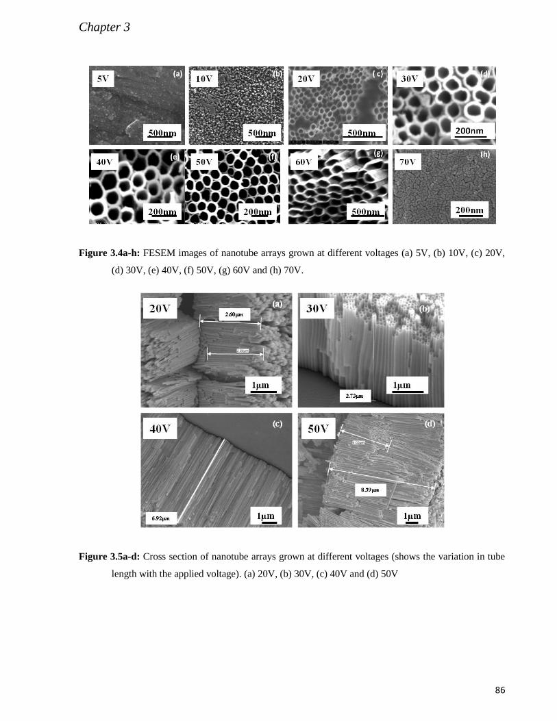
Chapter 3
86
Figure 3.4a-h: FESEM images of nanotube arrays grown at different voltages (a) 5V, (b) 10V, (c) 20V,
(d) 30V, (e) 40V, (f) 50V, (g) 60V and (h) 70V.
Figure 3.5a-d: Cross section of nanotube arrays grown at different voltages (shows the variation in tube
length with the applied voltage). (a) 20V, (b) 30V, (c) 40V and (d) 50V

Chapter 3
87
Figure 3.6a-b: (a) Variation of inner pore diameter of the nanotubes with voltage, (b) Variation of
nanotube length with applied voltage
3.3.1.2.2. Effect of Anodization Time
The changes in the morphological parameters with anodization time were investigated by
anodizing at 40 V at various time intervals, keeping all the other parameters similar. Variation in
surface morphology with time can be seen from the FESEM images given in Figure 3.7(a-l). In
the initial stages of anodization, the Ti surface transformed to a rough surface which gradually
changed to porous like structure and eventually converted to nanotubular morphology. The
formation of distinct nanotubular structure of ~1 micro meter length, from the porous structure,
occurred at around 20 to 25 minutes. Formation of well separated nanotubes could be discerned
after 1 hour of anodization. From the above observations, it is unambiguous that the
morphological parameters such tube diameter and length can be tuned by adjusting anodization
time, keeping all other parameters same. Compared to anodization in aqueous media, nanotubes
of ~1 micro meter length were obtained in the organic media within 25 minutes. This is because
of the decrease in the chemical dissolution rate at neutral pH. For application in photo catalysis

Chapter 3
88
Figure 3.7a-l: FESEM images showing the variation of surface morphology of Ti metal with the
anodization time showing the formation of nanotube arrays. (a) 0 minute, (b) 1 minutes, (c) 2
minutes, (d) 3 minutes, (e) 5 minutes, (f) 10 minutes, (g) 15 minutes, (h) 30 minutes, (i) 1 hours,
(j) 2 hours, (k) 4 hours and (l) 6 hours
and solar cells, since the diffusion length plays a major role, tuning the length of the nanotubes
with time and voltage is of paramount importance.
3.3.1.2.3. Effect of Electrolyte Composition
To study the effects of electrolyte composition on tube formation, anodization was
carried out at various water and ammonium fluoride concentrations in ethylene glycol.
3.3.1.2.3.1. Effect of water
Experiments were performed to elucidate the effect of water content keeping the
ammonium fluoride concentration a constant (0.5 wt %). The anodization experiments were

Chapter 3
89
carried out at 40 V for two hours. Figure 3.8(a-c) depicts the morphology of Ti anodized at water
contents of 2.5, 10 and 20 wt%. An increase in tube diameter with increase in water content was
observed. As the water content increased, number of H+ ions per unit area at the electrode
increased resulting in higher chemical dissolution rate and hence changes in current density. This
resulted in the formation of ripple like structure on the wall of the nanotubes. The observed tube
diameters are 77 ±7 nm (2.5wt% water), 97 ±14 nm (10wt%water) and 152 ±16 nm
(20wt%water). Formation of ripple like structure on the walls of the nanotubes was observed in
excess of 5 wt% of water and that increased with water content. When the water content was 20
wt%, the system behaved almost like an aqueous medium and the rate of chemical dissolution
increased leading to nanotube arrays having ripples on the tube walls. The above observations
indicate that the water content affect tube wall morphology as well as diameter. When the water
content was low, smooth walled TiO2 nanotubes, ideal for specific applications where the
electron transfer efficiency should be higher, could easily be grown.
Figure 3.8a - c: Surface morphology of the anodized Ti foils at different weight percent of water. (a) 2.5
wt%, (b) 10 wt% and (c) 20 wt%
3.3.1.2.3.2. Effect of ammonium fluoride
The concentration of ammonium fluoride was varied from 0 wt% to 5 wt% in the
electrolytic bath keeping the water content at the optimum level (2.5 wt %) determined from the

Chapter 3
90
experiments described in the previous section. The applied potential and anodization time were
kept at 40V and 2 hours respectively. Figure 3.9(a-e) shows the SEM images of the surface
anodized at different concentrations of NH4F.
Anodization in fluoride free solutions resulted in the formation of compact oxide layer
without nanotubes. When the NH4F concentrations were 0.5, 1, 2 and 5 wt%, nanotube formation
was observed, indicating the need of fluoride ions for the formation of self organized TiO2
nanotubes. Even though nanotube formation was observed at 0.5, 1 and 2 wt % of NH4F,
homogenous nanotubes were observed only at 0.5 wt%. At higher concentrations of NH4F, the
nanotube arrays were covered with grass like structures which might have formed due to the
removal of nanotubes from the substrate. In the case of anodized Ti, where the fluoride ion
concentration was 5 wt%, distinct tubular structures were not observed (Figure 3.9e).
Figure 3.9a-e: Surface morphology of the anodized Titanium samples at different weight percent of
NH4F. (a) Ti surface anodized without adding NH4F, (b) 0.5 wt%, (c) 1 wt%, (d) 2 wt% and (e) 5
wt% of NH4F.

Chapter 3
91
No substantial change in tube length or diameter could be discerned with the change in
concentration. The observed diameters are, 77 ± 7nm (0.5 wt% NH4F), 86 ± 9nm (1wt % NH4F)
and 80 ± 7nm (2 wt% NH4F). Based on these results and those reported in the literature18
, NH4F
content in the range 0.2 to 0.5 wt% can be considered as the optimum range for obtaining smooth
walled nanotube arrays.
3.3.1.3. Effect of annealing temperature on crystallinity and morphology:
The as prepared samples, upon XRD analysis, were found to be amorphous and hence
annealed at various temperatures to study evolution of phases as different phases of the material
are preferred for specific applications. The XRD pattern of the as prepared TNTA as given in
Figure 10a shows amorphous nature which is in agreement with the results obtained by Oomman
et al.71
The observed peaks correspond to Ti substrate. In order to study the evolution of phases,
the as prepared nanotube arrays were annealed in air at 400, 500, 600 and 700 oC for 2 hours and
the corresponding XRD patterns were recorded. Figure 3.10b shows the XRD pattern of the
annealed samples. At 400oC, there were peaks corresponding to tetragonal anatase phase of TiO2
in addition to the substrate peak. When the samples were annealed at 500oC, the anatase peaks
got sharpened and intensified indicating increase in anatase phase crystallinity and crystallite
size. The observed low intensity peak (27.4o) corresponding to rutile phase indicates the
beginning of phase transformation. The XRD pattern of the sample annealed at 600o
C revealed
the presence of both rutile and anatase phases. At 700oC, anatase and rutile phases were still
present but with higher concentration of rutile phase. The phase transformation behavior
observed here was slightly different from those reported by Oomman et al71
, where phase
transformations took place at higher temperatures. These changes can be attributed to the
difference in the heating rate and annealing duration.

Chapter 3
92
Figure 3.10a-b: (a) XRD pattern of the as prepared TiO2 nanotubes (shows that the samples are
amorphous). b. XRD pattern of TiO2 nanotubes annealed at different temperature
In order to verify the effect of temperature on tube morphology, FESEM analysis of the
nanotube arrays were carried out. Figure 3.11(a-d) and 3.12(a-c) show the surface morphology
and cross sectional views, respectively, of the nanotube arrays annealed at different
temperatures, clearly depicting the effect of calcination temperature on tube morphology. From
the surface topography, it is clear that the samples annealed at 400 and 500 oC, retains their
tubular architecture. Whereas, the samples annealed at 600 and 700oC have tubes with closed
mouth, due to wall thickening. However, the cross sectional view clearly indicate retention of
tubular morphology even up to 700 oC.
The occurrence of anatase to rutile phase transformation at 500 to 600 °C as inferred
from XRD results and can be correlated with the SEM images. Phase transformation from
anatase to rutile requires crystal reorientation and growth72
and is achieved with increase in
temperature. It has been reported that phase stability, crystal growth and nucleation are
dependent on crystallite size.73
Below 14 nm anatase is the stable phase.73
In our study, the
crystallite size of the nanotube arrays annealed at the lowest temperature (400oC) is ~48 nm, and

Chapter 3
93
therefore is prone to phase transformation. Gouma et al in 2001 investigated the defect
mechanism of phase transformation in vacuum and hydrogen reduced TiO2 samples.74
The
anatase to rutile transformation involves the breakup of anatase structure with a volume change
of about 8%. This collapse occurs by the deformation of the oxygen frame work and shifting of
the Ti4+
ions by rupturing two of the six Ti-O bonds to form new bonds73
and hence the phase
transformation is affected by the presence of hydroxyl ions chemisorbed on the TiO2 surface.
Figure 12d illustrates the variation of anatase crystallite size with annealing temperature. The
101 diffraction peak of the anatase phase is considered here for the crystallite size calculation.
While increasing temperature from 600oC to 700
oC there is a drastic change in the crystallite size
variation which evidently depicts the increase in crystal growth kinetic rate in this temperature
range. Hebrard and Nortier investigated the effect of hydroxyl species in the sintering and
crystallite growth of TiO2 powders and found that surface diffusion of hydroxyl species is the
most likely rate limiting step of the particle growth in case of anatase TiO2 powder.75
Figure 3.11a-d: SEM images showing the surface morphology of annealed TNTA (a) at 400oC (b) at
500oC (c) at 600
oC and (d) at 700
oC

Chapter 3
94
Figure3.12a-d: SEM images showing the cross sectional views of annealed TNTA (a) at 400oC (b) at
600oC and (c) at 700
oC and (d) Variation of anatase crystallite size with temperature.
The increase in oxygen and titanium ion diffusion rate is due to the presence of hydroxyl
species on the TiO2 surface. The presence of surface OH groups was clearly identified by XPS
measurements which will be discussed in the section 3.3.1.4. The diffusion process creates
annihilation of cation and anion vacancies thereby facilitating the crystal growth. An increase in
the crystallite size of anatase phase TiO2 will enhance the rutile phase transformation rate and
occurs by consuming the anatase crystallites present at the nanotube walls. As the process
continues, complete transformation occurs leading to the destruction of the tubular morphology
and there by generating thick rutile films.71
Based on the above results, the optimum process parameters for obtaining smooth walled,
homogenous vertically aligned TNTA on Ti foils, at room temperature, are 30 – 50 V
anodization potential, 2 hours anodization time, electrolyte composition of 0.5 wt% NH4F and
2.5 wt% H2O in ethylene glycol. Anatase TNTA are obtained by annealing the samples at 400
oC.
As transparent TNTA films are required for application in devices like DSSCs, for better
efficiency, the same were also prepared by anodizing Ti thin films deposited on FTO coated
glasses.

Chapter 3
95
Titanium thin films of good adherence were obtained by RF magnetron sputtering at an
RF power of 300 W and substrate temperature 300oC. The film adherence was checked with
scotch tape test and found to be adherent. The deposition rate and film thickness were found to
be 20 nm/min and ~1 micrometer respectively. Based on the obtained optimum process
parameters for the synthesis of TNTA on Ti foils, anodization of Ti thin films grown on FTO
coated glasses were carried out at 40V in 0.5wt% NH4F + 2.5wt% water + ethylene glycol. The
potentiostatic transients obtained are similar to the one obtained in the case anodization of Ti
foils indicating prevalence of similar nanotube formation mechanism. The FESEM images of the
samples anodized at different time intervals (2, 3 and 4 hours) are given in Figure 3.13a-c. From
figure 3.13 it can be discerned that 2 hours of anodization resulted in comparatively debris free
nanotubular architecture having mean tube diameter of 60±7nm.
Figure 3.13a-c: FESEM image of the samples anodized at 40V by anodizing at different time intervals ie;
(a) 2, (b) 3 and (c) 4 hours.
It is evident from the SEM images that with increase in anodization time precipitates
were formed leading to nanotube collapse. At the end of 4h, scales like features were observed
(Figure 3.13c). From the above it can be said that under the present experimental conditions
transparent TNTA thin films on FTO coated glasses are obtained on anodizing Ti films in
ethylene glycol medium containing 0.5wt% NH4F and 2.5wt% water for duration of 2h. The as

Chapter 3
96
prepared TNTA on FTO glasses were amorphous and upon annealing at 400oC, these samples
got crystallized to anatase phase as in the case TiO2 nanotubes grown on foils.
3.3.1.4. X-ray photoelectron spectroscopic analysis
The composition and the types of oxygen species (lattice O (Ti4+
- O), O (Ti3+
-O, i.e
oxygen near an oxygen vacancy), OH and H2O) present in the as prepared as well as annealed
TNTA were studied by using XPS. Based on the results of FESEM and XRD, TNTA and
transparent TNTA films on FTO coated glasses having best morphology were obtained on
anodizing Ti foils and Ti films in ethylene glycol medium containing 0.5wt% NH4F and 2.5wt%
water at 40V for 2h. Hence these samples were chosen for XPS studies. Among annealed
samples those annealed at 400 oC were chosen as they have intact tubular morphology with good
anatase phase crystallinity. Stoichiometric TiO2 consists of Ti4+
and O2-
ions. It is well
understood that TiO2 synthesized by various techniques exhibits nonstoichiometry and it varies
with synthesis technique.76
Figure14a shows the high resolution XPS spectra of Ti 2p core levels
of as prepared TNTA on Ti foil. From the spectra, it can be seen that the core level of Ti 2p1/2
and Ti 2p3/2 peak positions are at 465. 3 and 459.4 eV, respectively, and is assigned as Ti4+
peak,
with a peak separation of 5.9 eV. The peaks are asymmetric indicating the presence of lower
valent Ti ions. In order to distinguish the Ti ions of different valancies peak fitting of the spectra
were performed using XPS fit software. The electron background correction was carried out
using Shirley (nonlinear) background correction method77
which is commonly accepted and
widely used one among the various background correction methods.77,78,79
For the background
correction, the energy window chosen was 468.17 to 452.57eV. The background corrected
spectra were fitted by assuming Gaussian profiles for different chemical states. The parameters
which define the XPS core level peaks are peak position or binding energy, full width at half

Chapter 3
97
maximum (FWHM), peak area and peak intensity. The Ti4+
2p spin orbit components have to
confirm the energy difference of 5.7 eV for Ti 2p1/2 and Ti 2p3/2 states80
and intensity ratio of 0.5.
The energy difference between the spin orbit components of Ti0 is fixed as 6.15 eV.
81 By
intricate peak fitting process the spectra have been resolved into eight spin orbit components
resolved at 2p3/2 binding energies 459.45, 458.38, 457.44, 454.76 eV and their corresponding
2p1/2 components (465.28, 464.31, 463.04, 460.72 eV) which are assigned as Ti4+
(TiO2), Ti3+
(TiOOH), Ti3+
(co-ordinatively unsaturated i.e Ti3+
adjacent to oxygen vaccancy) and Ti0 (Ti),
respectively. The binding energy values agree with the reported values.82-84
Although some
studies show the presence of Ti2+
in their analysis82,
84
, in the present study, the existence of Ti2+
state was not identified. The low intensity peak at 454.76 eV corresponding to Ti0 is from the Ti
substrate as the oxide film formed was highly porous and cracked.
Different types of oxygen species (lattice O, oxygen near an oxygen vacancy, OH and
H2O) present are distinguished by the different O1s binding energies. Figure15a shows the
deconvoluted O 1s spectrum of the as prepared TNTA. The asymmetric peak was deconvoluted
to three components with minimum chi square by the same peak fitting process, where the
window for the peak fitting process was 536 to 526 eV. The peak positions, 530.67 (Ti4+
-O),
531.16 (Ti3+
-O i.e. oxygen near an oxygen vacancy) and 532.3 eV (Ti-OH/OH-), agree well with
reported literature values.82
The peak corresponding to the binding energy value of 532.29
reveals the presence of Ti(OH)xOy and is supported by FTIR analysis where, the presence of
hydroxyl group is revealed.
The XPS analyses were also performed at the Ti/TiO2 interface. TNTA were peeled off
from the Ti substrate and the XPS analysis was carried out at that region. Figure14c shows the
deconvoluted XPS spectra at the interface (Ti/TiO2). The presence of Ti2+
at the metal/oxide

Chapter 3
98
interface can be attributed to the partial oxidation of Ti metal during electrochemical
anodization. Since peak corresponding to Ti2+
could not be seen in the deconvoluted Ti 2p
spectra of nanotube arrays, it can be inferred that as one moves from metal / oxide to oxide /
electrolyte interface, the atomic fraction of Ti2+
decreases. The trend is reflected in the O1s
spectra too (Figure 3.15c). The amorphous TiO2 film grows at the Ti/oxide and oxide/electrolyte
interfaces by the simultaneous inward and outward migration of anions and cations, respectively.
As Ti2+
ions migrate towards the film/electrolyte interface, these are oxidized to higher valent
states by the incoming oxide ions and therefore Ti2+
ions are not observed at the film surface. In
view of the above and at any point of time, the TiO2 films formed will be oxygen deficient and
depict nonstoichiometry.
The as prepared amorphous TiO2 nanotubes, upon annealing at 400 oC, were transformed
to anatase phase. Figure14b shows the deconvoluted Ti2p spectra of annealed nanotube arrays.
The spectra were deconvoluted and resolved into six spin orbit components at 2p3/2 binding
energies 459.49, 458.58, 457.44 eV and their corresponding 2p1/2 components (465.28, 464.09,
463.165) which are assigned as Ti4+
( TiO2), Ti3+
( TiOOH) and Ti3+
(coordinatively unsaturated
i.e Ti3+
adjacent to oxygen vacancy). Peak corresponding to Ti0 (substrate) was not observed as
the substrate got oxidized during annealing. However, peak corresponding to Ti3+
state was
identified as indicative of the presence of oxygen vacancies. Figure 3.15b shows the
deconvoluted oxygen 1s spectra of the annealed TiO2. The peaks observed are located at
530.73(Ti4+
-O), 531.24(Ti3+
-O) and 532.10 eV (Ti-OH/OH-). To verify the stoichiometry, the
atomic ratios (concentrations) were calculated from the peak areas by taking into account the
relative sensitivity factors for individual elements, since the area under the curves doesn’t

Chapter 3
99
directly give the atomic ratio. From the high resolution Ti-2p, O-1s spectra the atom fractions of
Ti and O were calculated using the following equations
(5)
(6)
Table 3.1 shows the fraction of different ‘Ti’ and ‘O’ species present at the surface as well as at
the metal – oxide interface of the as prepared and annealed TiO2 nanotubes. An excess of O at
the surface compared to the stoichiometric composition of TiO2, arises due to the presence of
Ti(OH)xOy species like Ti(OH)3, Ti(OH)2O and Ti(OH)4.
Figure 3.14a-c: Deconvoluted high resolution Ti 2p spectra (a) at the surface, (b) nanotube arrays
annealed at 673K and (c) at the interface (Ti/TiO2), as prepared.

Chapter 3
100
Figure 3.15a-c: Deconvoluted high resolution O1s spectra (a) at the surface (amorphous TiO2), (b) of
nanotube arrays annealed at 673K and (c) at the metal-oxide interface.
Chemical state Atom fraction at the
surface (amorphous)
Atom fraction of Ti at the
Interface (amorphous)
Atom fraction of Ti
(annealed at 673K)
Ti O Ti O Ti O
Ti4+
0.154 0.360 0.127 0.355 0.221 0.444
Ti(OH)xOy 0.065 0.099 0.029 0.098 0.072 0.066
Ti3+
0.079 0.241 0.037 0.272 0.024 0.172
Ti2+
- - 0.058 0.023 - -
Table 3.1: Fraction of Ti species and O species present at the surface and the interface of the as prepared
and annealed TNTA.
The Ti 2p and O1s spectra of as prepared as well as annealed nanotube arrays confirm the
presence of lower valent Ti ions and oxygen vacancies. The oxygen vacancies at the surface
take the form of missing oxide ions in the Ti-O-Ti row (oxygen vacancies i.e. Ti3+
- VO – Ti3+
)

Chapter 3
101
leading to the formation of coordinatively unsaturated Ti3+
ions. These Ti3+
ions have distorted
coordination geometry because of adjacent oxide ion vacancies. They have a tendency to form
additional coordination and therefore the oxygen vacancies act as adsorption sites for organic
and water molecules thereby playing an important role in the photo-oxidation of organic
species.85
When water molecules come in contact with nanotube surface they are adsorbed at the
bridging oxygen vacancies and dissociated into OH and H. The OH group fills the oxygen
vacancy to form Ti – OH – Ti / Ti-(OH)2-Ti bridge.85
The hydrogen atom has two options. It can
either form an identical Ti – OH – Ti bridge, by binding to another Ti – O – Ti bridge or, Ti3+
-
OH by binding to O2-
ions terminating at the surface. As anions are easily polarizable by cations
they terminate at the surface thereby reducing the surface potential and constitute active sites for
reaction with the H atoms to form Ti3+
- OH.60
Hydroxylation at the bridging oxygen vacancies
was elucidated by Wendt et al on the basis of results from scanning tunneling microscopic
studies on reduced TiO2 (110) surface and density functional theory calculations.86
Hence,
presence of bridging oxygen vacancies is a necessary condition for water dissociation or organic
oxidation and has immense influence on the photocatalytic properties of TiO2. Based on above
observations the expected oxygen species can be enumerated as Ti4+
- O, Ti4+
- (OH)2, Ti3+
- O,
Ti3.5+
- OH – Ti3.5+
and Ti3+
- OH. In addition, the presence of H2O molecules adsorbed on to the
OH groups by hydrogen bonding cannot be excluded.85
Although the surface bridging oxygen
vacancies are filled by OH groups still there are O1s peaks corresponding to oxygen near oxygen
vacancies and Ti 2p3/2 peaks corresponding to coordinatively unsaturated Ti3+
because of
presence of bulk defects.85
The bridging oxygen vacancies modify the electronic structure by
introducing band gap states, ~0.75 eV, below the conduction band and their population increases
in direct proportion with the density of bridging oxygen vacancy.87
This will enhance electronic

Chapter 3
102
properties like conduction and field emission.60
Hence synthesis of oxygen deficient TNTA is
vital for application in the area of photocatalytic, photo voltaic and electronic devices.
Presence of fluorine was detected both in the case of as prepared (Figure 3.16a) as well as
annealed samples (Figure 3.16c) by XPS analysis. The binding energy value of 685 eV
corresponds to adsorbed fluoride ions. Fluoride ions were also observed at the surface and metal-
oxide interface (figure 3.16b) before and after sputtering for different time periods.
Figure 3.16a-c: (a) Flourine 1s spectra of amorphous TiO2 sample. Reveals the presence of flourine at
different depths. (b) Flourine 1s spectra of amorphous TiO2 sample (at the interface). From the
spectra it is evident that the flouride is present at the metal/oxide interface and reveals that
flouride ion is playing an important role in the tubular morphology of Titania and (c) Flourine 1s
spectra of annealed TiO2 sample. Even after annealing at 673K the flourine presence is seen.
From these observations, it can be concluded that fluoride ions migrate along with the
oxygen ions to the metal - oxide interface which facilitates the growth of TiO2 nanotubes.
Habazaki et al reported that fluoride ions migrate inward at a rate twice that of O2-
ions,
developing a thin layer of increased fluoride content between the anodic oxide and the metal
substrate.88
The same is also observed by Albu et al.89
The observed F 1s binding energy (684.3
eV) corresponds to adsorbed F- ions. Peaks corresponding to lattice F
- ions (688.5 eV) could not

Chapter 3
103
be detected. The incorporated fluoride ions are sensitive to annealing and are eliminated at
higher temperatures.50
To study the composition of transparent TNTA films on FTO coated glasses, the X-ray
photoelectron spectra of annealed samples were required as in the case of TNTA on foils. The Ti
2p spectra of transparent TNTA (Figure 3.17a) were deconvoluted to six spin orbit components
(2p3/2 and 2p1/2 ) at 459.5, 458.7, 457.44, 465.34, 464.39 and463.15 eV. These are assigned as
Ti4+
(TiO2), Ti3+
(TiOOH), Ti3+
(co-ordinatively unsaturated i.e Ti3+
adjacent to oxygen
vacancy). Different types of oxygen species present are distinguished by different oxygen
binding energies observed for O1s spectra. The asymmetric oxygen 1s spectra (Figure 3.17b)
were deconvoluted and resolved into three components which are positioned at 530.71, 538.18
and 532.06 eV. The peak positions, 530.67 (Ti4+
-O), 531.16 (Ti3+
-O i.e. oxygen near an oxygen
vacancy) and 532.3 eV (Ti-OH/OH-), agree well with the results of TNTA on foils. The
nonstoichiometry in the TNTA thin film is similar to that of TNTA on foils and it arises due to
bridging oxygen vacancies, which modify the electronic structure and enhances the electronic
properties.
Figure 3.17a-b: (a) the deconvoluted 2p spectra of Ti and (b) the deconvoluted 1s spectra of O

Chapter 3
104
3.3.1.5. FTIR analysis
The FTIR spectra of the pristine TNTA synthesized at 40 V and annealed at 400 oC are
shown in Figure 3.18. The stretching and bending vibrational peaks of OH groups at 3000-3400
cm-1
and 1626.15 cm-1
in the spectra confirm the presence of hydroxyl species. The broad peak
in the range 400-800 cm-1
corresponds to bulk TiO2. These observations are in agreement with
the reported values11, 82, 90
and confirm the XPS results.
Figure 3.18: FTIR spectra of the as prepared sample anodized at 40V for 2 hours
3.3.1.6. UV-Visible spectroscopic analysis
Figure 3.19a and b shows the DRS and absorbance spectra of the pristine TNTA on foils
and on FTO glass, respectively (anodized at 40V for 2 hours and annealed at 400oC). The optical
band gap values are calculated from the Tauc plots obtained from the DRS and absorbance
spectra as explained in chapter 2. The optical band gap, obtained by extending the line, from the
slope of the linear part of the curve, in the Tauc plot (Figure 3.20a), to x = 0 was calculated and
has a value of 3.27. In case of TNTA on FTO glass the band gap calculated turns out to be 2.8

Chapter 3
105
eV and is represented in Figure 3.20b. The analysis reveals that the material absorbs in the ultra
violet region.
Figure 3.19a-b: (a) DRS spectra of the pristine TNTA on foils, (b) Absorbance spectra of TNTA on FTO
glass
Figure 3.20a-b: Tauc plot of the (a) pristine TNTA on foils, (b) TNTA on FTO glass
3.3.2. Nitrogen Doped TiO2 nanotube arrays.
3.3.2.1. Mechanism and micro-structural analysis
Based on the earlier results, that anodization of Ti foils in ethylene glycol / H2O / NH4F
electrolyte, corresponding to the composition 2.5 wt% H2O and 0.3 to 0.5 wt% NH4F, yielded
smooth walled nanotubes with maximum possible growth rate. Syntheses of N-doped TNTA

Chapter 3
106
were carried out in same electrolyte composition with different weight percent of urea (0.1, 0.2
and 0.3) as nitrogen precursor. Urea was chosen as a nitrogen source, as electrolysis of aqueous
solutions containing urea decomposes to N2 and CO2 at high anodic potentials.91
Since nitrogen
formed at the anode surface will be nascent, before being liberated as N2, there exists the
possibility of nitrogen incorporation into the anion lattice of TiO2 during the formation of TNTA.
Also one can expect a variation in the amount of nitrogen substituted for oxygen in the anion sub
lattice with nitrogen precursor (urea) concentration. The potentiostatic transient obtained is quite
similar to the conventional one obtained during Ti anodization in the medium without urea. Also
the charge (area under the current density Vs time curve) is not much different from that in
which anodization has been carried out without urea. This implies similar mechanism prevailing
for pristine and N-doped TiO2 nanotube formation. Anodization was carried out as a function of
applied potential to delineate the optimum potential range for the synthesis of smooth walled
nanotube arrays. The surface topography of Ti foils anodized at different potentials varying from
20 to 60V for 2 hrs, corresponding to 0.2 wt% urea is shown in Figure 3.21 (a-e). Similar
micrographs were obtained for other urea concentrations. Figure 3.21f shows the cross sectional
FESEM image of the N-doped TNTA. At 10V, porous structures were formed on the Ti surface,
but no distinct nanotubes are observed. However, formation of distinct nanotubes having inner
diameter of ~47 nm is observed, when the applied potential was increased to 20V, from the SEM
image. The above observation indicates that there is a minimum required potential for the
formation of N-doped self-organized nanotubes as in the case of formation of pristine TiO2
nanotubes. Under the present experimental conditions, the minimum required potential for the
formation of N-doped nanotubes is around 20 V. As reported in the case of pristine TNTA,
formations of self aligned nanotube arrays were observed up to a potential of 60 V. A careful

Chapter 3
107
observation of the SEM pictures shows that the best homogeneous morphology is obtained when
synthesis is carried out at 40 V (similar to the case of pristine TNTA). Figure 3.22 shows the
variation of inner diameter of the nanotubes with applied potential. The increase in tube diameter
with voltage can be attributed to the enhanced chemical dissolution of TiO2 at the pore wall. No
significant variations in wall thickness were observed compared to the pristine samples. The
variation in wall thickness with respect to applied voltage is shown in the inset of Figure 3.22.
Figure 3.21a-f: Surface morphology of anatase N-doped TNTA synthesized at (a) 20 V, (b) 30 V, (c) 40
V, (d) 50 V, (e) 60 V and (f) cross section of nanotube arrays.
When the potential is increased, rate of chemical dissolution and oxidation increases
resulting in nanotube growth. When the applied potential was 80 V, the current density increased
with time and nano-tubes were not observed on the foil even after two hours of anodization
attempt. This is similar to the case of pristine TNTA. Here too, the electrolyte temperature
increased with applied potential enhancing the chemical dissolution.
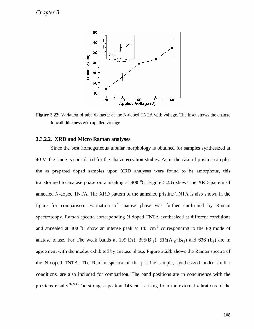
Chapter 3
108
Figure 3.22: Variation of tube diameter of the N-doped TNTA with voltage. The inset shows the change
in wall thickness with applied voltage.
3.3.2.2. XRD and Micro Raman analyses
Since the best homogeneous tubular morphology is obtained for samples synthesized at
40 V, the same is considered for the characterization studies. As in the case of pristine samples
the as prepared doped samples upon XRD analyses were found to be amorphous, this
transformed to anatase phase on annealing at 400 oC. Figure 3.23a shows the XRD pattern of
annealed N-doped TNTA. The XRD pattern of the annealed pristine TNTA is also shown in the
figure for comparison. Formation of anatase phase was further confirmed by Raman
spectroscopy. Raman spectra corresponding N-doped TNTA synthesized at different conditions
and annealed at 400 oC show an intense peak at 145 cm
-1 corresponding to the Eg mode of
anatase phase. For The weak bands at 199(Eg), 395(B1g), 516(A1g+B1g) and 636 (Eg) are in
agreement with the modes exhibited by anatase phase. Figure 3.23b shows the Raman spectra of
the N-doped TNTA. The Raman spectra of the pristine sample, synthesized under similar
conditions, are also included for comparison. The band positions are in concurrence with the
previous results.92,93
The strongest peak at 145 cm-1
arising from the external vibrations of the

Chapter 3
109
anatase crystal structure, indicates that long range order pertaining to anatase crystallinity has
evolved in the annealed N-doped TNTA. Compared to the pristine one, the highly intense Eg
mode (145 cm-1
) of the doped TNTA shows a red shift (inset of Figure 3.23 b). This can be
ascribed to the change in force constant due to nitrogen doping.
Figure 3.23a-b: (a) XRD pattern of N-doped and pristine TNTA. (b) Visible micro Raman spectra of the
N-doped and pristine TiO2
3.3.2.3. XPS investigations.
As in the case of pristine TNTA, to study the composition as well as nitrogen
incorporation to the crystal, XPS studies were carried out. Figure 3.24a-d shows the
deconvoluted Ti 2p spectra of TNTA synthesized at different wt% of urea and annealed at 400
oC. The spectrum of the pristine TiO2 is also included for comparison. The peaks are
deconvoluted into four different peaks. The region shows four doublets: the peaks at 459.4,
458.0, 456.9 and 455.6 eV correspond to the 2p3/2 region suggesting Ti (+4)-O, Ti (+3)-O, Ti
(+3)-N or Ti (+3)-OH and Ti (+2)-O, respectively. The other peaks at higher binding energies
corresponding to the 2p1/2 core level of the respective states. The O 1s spectra of the
corresponding samples are shown in Figure 25 a-d. The deconvoluted peaks positioned at 530.5,

Chapter 3
110
530.9 and 531.9 eV correspond to O-Ti (+3), O-Ti(+4) and HO-Ti(+3,+4), respectively, in
agreement with the reported values.83,85
The high resolution N-1s spectra of the samples synthesized at different wt% of urea are
shown in figures 3.26a (0.1 wt %), 3.26b (0.2 wt %) and 3.26c (0.3 wt %). The data for the
analysis are required at a sputter depth arrived after 3 minutes of sputtering (10 nm/min) for all
the samples. This was done to obtain a reasonable intensity for nitrogen signal. The high
resolution N-1s spectra consist essentially of three peaks viz. one high intensity asymmetric peak
around 396.8 eV and two low intensity peaks at 400.2 and 403.1 eV respectively. The high
intensity asymmetric peak has been deconvoluted to high and low intensity peaks at 396.8 eV
and 397.6 eV, respectively. The different N-1s BE values represent different electron density
around nitrogen suggesting various N coordination environments in the lattice. Based on the
references given in the introduction, the N-1s peak at 400.2 can be assigned to Ni. The peak
observed at 403.1 eV is assigned to surface adsorbed NOx species.46,49, 94
The two deconvoluted
peaks in the range 396 – 398 eV (396.8 and 397.6 eV) can be ascribed to substitutional nitrogen
in the oxide lattice. The structure of anatase TiO2 consists of corner and edge sharing (TiO6)
octahedra. If the number of oxygen atoms substituted by nitrogen atoms in each octahedron is
same (nitrogen substitution is uniformly distributed throughout), one would expect a single N-1s
BE value corresponding to NO (N-Ti-O) species. If the number of N ions in the co-ordination
sphere around Ti varies, the observed N-1s values will lie in a range leading to N-1s peak
broadening and asymmetry. In such a situation, the asymmetric peak on deconvolution shows up
different BE values. In addition, when two oxygen atoms are substituted by nitrogen atoms one
oxygen vacancy is generated.

Chapter 3
111
Figure 3.24a-d: High resolution Ti 2p x-ray photoelectron spectra (a) pristine TNTA (b) N doped TNTA
anodized 0.1 wt % of urea containing electrolyte(c) 0.2 wt % of urea containing electrolyte
and(d) 0.3 wt % of urea containing electrolyte
Figure 3.25a-d: High resolution O 1s x-ray photoelectron spectra (a) pristine TNTA (b) N doped TNTA
anodized 0.1 wt % of urea containing electrolyte, (c) 0.2 wt % of urea containing electrolyte and
(d) 0.3 wt % of urea containing electrolyte

Chapter 3
112
Figure 3.26a-c: High resolution N 1s X-ray photoelectron spectra (a) TiO1.85N0.115 (b) TiO1.813N0.14 (c)
TiO1.84N0.121
This will distort the coordination octahedra having vacancies, as neighboring anions relax
towards the vacancy, adding small changes to N-1s BE values. Since the electrochemical doping
is achieved at ~298 K, equilibrium cannot be expected and therefore there exist the possibility of
variation in the number of oxygen atoms substituted by nitrogen atoms in various coordination
octahedra present in the lattice. Hence the reason for observing, on deconvolution, N-1s BE
values at 396.8 and 397.6 eV, corresponds to substitutional nitrogen in the oxide ion lattice. The
atom fractions of Ti, O and N are calculated using the following equations
(7)
(8)
(9)

Chapter 3
113
IN-1s is the peak area of the N-1s peak corresponding to O-Ti-N, ITi-2p is the sum of the areas of
the Ti2p deconvoluted peaks (Figure 3.25 (a-d)) and IO-1s is the area of the O-1s peak (26(a-d))
corresponding to bonded oxygen and STi, SO and SN corresponding atomic sensitivity factors.
Based on the calculated atom fractions, and taking into account the fraction of Ti3+
ions, the
chemical formula of N-doped TiO2 is represented as TiO1.85N0.115, TiO1.813N0.14 and TiO1.84N0.121
for the samples synthesized at 0.1, 0.2 and 0.3 wt% of urea in the electrolyte, respectively. The
corresponding atom percent of nitrogen are about 3.88, 4.74 and 4.12, respectively.
3.3.2.4. Diffuse reflectance measurements
Figure 3.27a and b shows the Tauc plots of different nitrogen doped samples. Tauc plot
of the pristine TNTA is also included for comparison. The optical band gap, obtained by
extending the line, from the slope of the linear part of the curve, to x = 0 was calculated and are
3.27. 3.22 2.75 and 2.77 eV for pristine TiO2, TiO1.85N0.115, TiO1.813N0.14 and TiO1.84N0.121,
respectively. In the case of TiO1.813N0.14, the Tauc plot show an extra linear part of which
intercept at x=0 shows transition state situated at a difference of 2.59 eV.
Figure 3.27: Diffuse Reflectance spectra of pristine as well as N-doped TiO2

Chapter 3
114
This shows that due to nitrogen doping certain interband electronic states have been generated.
In the case of N- doped samples, the band gaps have been shifted to lower values than that of the
pristine TiO2. The observed shifts in the band gap energy for TiO1.85N0.115, TiO1.813N0.14 and
TiO1.84N0.121 with respect to that of pristine TiO2 are 0.05, 0.52 and 0.5 eV, respectively. The
extra state introduced in the case of TiO1.813N0.14 is located 0.68eV above the valence band.
3.4. Conclusion
Self aligned TNTA were synthesized on Ti substrates by electrochemical anodization
technique using fluoride ion containing organic electrolyte. Highly ordered nanotubes of about
few micrometer lengths were obtained in neutral pH within 1 hour of anodization duration. The
potentiostatic transients qualitatively revealed the mechanism of nanotube formation. From the
potentiostatic transients, correlating with reported results, it can be said that field assisted
chemical oxidation of Ti and field assisted chemical dissolution of TiO2 and Ti by fluoride ions
played a key role in nanotube formation. To understand the mechanism qualitatively, anodization
of Ti foils were carried out as a function of voltage, time and electrolyte composition. Desired
aspect ratio and wall morphology, depending upon the application, can be achieved by varying
the electrochemical parameters. The as prepared amorphous nanotube arrays transformed to
anatase phase on annealing at 400 oC. Anatase to rutile phase transformation was observed with
increase in temperature. Although the tubular surface morphology was found to be destroyed at
600 °C and above, the cross sectional SEM micrographs revealed retention of tubular
morphology up to a temperature of 700oC. The presence of different surface and subsurface
defect states arising from the bridging oxygen vacancies were confirmed from XPS and FTIR
measurements. The defect state detection by XPS analysis supports the enhanced photo catalytic
activity of TNTA. Existence of fluoride ions at various depths confirms their migration from

Chapter 3
115
surface to interface during anodization. The band gap of the annealed TNTA measured by
diffuse reflectance analysis was found to be 3.27 eV.
TiO2 nanotube thin films were synthesized by electrochemical anodization of Ti films
deposited on conducting glasses by magnetron sputtering. The crystallinity of the annealed TiO2
nanotube thin films was confirmed from XRD studies. The nonstoichiometry of the TNTA films
due to bridging hydroxyl groups were proved by X-ray photoelectron spectroscopy. The band
gap of the annealed TNTA measured by diffuse reflectance analysis was 3.36 eV indicating
absorption capabilities in the ultra violet region.
N-doped TNTA corresponding to the compositions TiO1.85N0.115, TiO1.813N0.14 and
TiO1.84N0.121 were synthesized in single step anodization in electrolyte containing different
weight percent of urea. XRD and micro Raman analysis revealed the anatase phase crystallinity
of the N-doped TNTA annealed at 400 oC. The XPS analysis confirmed nitrogen incorporation
into TiO2 matrix both in substitutional and interstitial form out of which major contribution
arises from the substitutional states. A considerable shift in the band gap of the material was
observed for the nitrogen doped samples and in the case of TiO1.813N0.14, introduction of an extra
interband electronic state was observed.

Chapter 3
116
References
1 Paulose, M.; Mor, G. K.; K.Varghese, O.; Shankar K.; Grimes, C. A., J Photochem. Photobiol. A: Chem., 2006,
178, 8-15
2 Nagaveni, K.; Sivalingam, G.; Hegde, M. S.; Madras, G., Environ. Sci. Tech., 2004, 38, 1600-1604.
3Tan, B.; Wu, Y., J. Phys. Chem. B, 2006, 110, 15932-15938.
4 Choi, S. Y.; Mamak, M.; Coombs, N.; Chopra N.; Ozin, G. A., Nano Lett., 2004, 4, 1231-1235.
5 Mor, G. K.; Varghese, O. K.; Paulose, M.; Ong K. G.; Grimes, C. A., Thin Solid Films, 2006, 496, 42-48
6 Nakade, S.; Kubo, W.; Saito, Y.; Kanzaki, T.; Kitamura, T.; Wada Y.; Yanagida, S., J. Phys. Chem. B, 2003, 107,
14244-14248.
7 Zhu, Y.; Li, H.; Koltypin, Y.; Hacohen Y. R.; Gedanken, A., Chemi. Comm., 2001, 46, 2616-2617.
8 Wu, J. M., J. Cryst. Growth, 2004, 269, 347-355.
9 Miao, Z.; Xu, D.; Ouyang, J.; Guo, G.; Zhao X.; Tang, Y., Nano Lett., 2002, 2, 717-720.
10 Su, C.; Hong, B. Y.; Tseng, C. M., Catal. Today 2004, 96 (3), 119-126.
11 Hayashi, H.; Torii, K., J.Mater. Chem.y 2002, 12 (12), 3671-3676.
12 Goossens, A.; Maloney, E.-L.; Schoonman, J., Chem. Vap. Deposition 1998, 4 (3), 109-114.
13 Zwilling, V.; Darque-Ceretti, E.; Boutry-Forveille, A.; David, D.; Perrin, M. Y.; Aucouturier, M., Surf. Inter.
Anal. 1999, 27 (7), 629-637.
14 Gong, D.; Grimes, C. A.; Varghese, O. K.; Hu, W.; Singh, R. S.; Chen, Z.; Dickey, E. C., J. Mater. Res. 2001, 16
(12), 3331-3334.
15 Mor, G. K.; Varghese, O. K.; Paulose, M.; Ong, K. G.; Grimes, C. A., Thin Solid Films 2006, 496 (1), 42-48.
16 Zhu, Y.; Li, H.; Koltypin, Y.; Hacohen, Y. R.; Gedanken, A., Chem. Comm. 2001, (24), 2616-2617.
17 Macak, J. M.; Tsuchiya, H.; Ghicov, A.; Yasuda, K.; Hahn, R.; Bauer, S.; Schmuki, P., Curr. Opinion. Solid State
Mater. Sci. 2007, 11 (1–2), 3-18.
18 Prakasam, H. E.; Shankar, K.; Paulose, M.; Varghese, O. K.; Grimes, C. A., J. Phys. Chem. C 2007, 111 (20),
7235-7241.
19 Narayanan, R.; Kwon, T.-Y.; Kim, K.-H., Mater. Lett. 2009, 63 (23), 2003-2006.
20 Macak, J. M.; Schmuki, P., Electrochim. Acta 2006, 52 (3), 1258-1264.
21 Paulose, M.; Shankar, K.; Yoriya, S.; Prakasam, H. E.; Varghese, O. K.; Mor, G. K.; Latempa, T. A.; Fitzgerald,
A.; Grimes, C. A., J. Phys. Chem. B 2006, 110 (33), 16179-16184.
22 Cai, Q.; Paulose, M.; Varghese, O. K.; Grimes, C. A., J. Mater. Res. 2005, 20 (01), 230-236.
23 Wang, J.; Lin, Z., Chem. Mater. 2008, 20 (4), 1257-1261.
24 Macak, J. M.; Zlamal, M.; Krysa, J.; Schmuki, P, Small 2007, 3 (2), 300-304.
25 Macák, J. M.; Tsuchiya, H.; Schmuki, P., Angew. Chem. Inter. Ed. 2005, 44 (14), 2100-2102.
26 Taveira, L. V.; Macak, J. M.; Tsuchiya, H.; Dick, L. F. P.; Schmuki, P., J. Electrochem. Soc. 2005, 152 (10),
B405-B410.
27 Wang, J.; Lin, Z., J. Phys. Chem. C 2009, 113 (10), 4026-4030.

Chapter 3
117
28
Macak, J. M.; Tsuchiya, H.; Berger, S.; Bauer, S.; Fujimoto, S.; Schmuki, P., Chem. Phy. Lett.2006, 428 (4–6),
421-425.
29 Varghese, O. K.; Paulose, M.; Grimes, C. A., Nat Nano 2009, 4 (9), 592-597.
30 G. K. Mor, H. E. Prakasam, O. K. Varghese, K. Shankar and C. A. Grimes, Nano Letters, 7 (2007) 2356-2364.
31 H. Zheng, A. Z. Sadek, M. Breedon, D. Yao, K. Latham, J. D. Plessis and K. Kalantar-Zadeh, Electrochem.
Comm., 2009, 11,1308-1311.
32 J. M. Macak, H. Tsuchiya, S. Berger, S. Bauer, S. Fujimoto and P. Schmuki, Chem. Phys. Lett, 2006, 428, 421-
425.
33 Mor, G. K.; Shankar, K.; Paulose, M.; Varghese, O. K.; Grimes, C. A., Nano Letters 2006, 6 (2), 215-218.
34 Mor, G. K.; Varghese, O. K.; Paulose, M.; Grimes, C. A., Adv. Func. Mater. 2005, 15 (8), 1291-1296.
35 Allain, E.; Besson, S.; Durand, C.; Moreau, M.; Gacoin, T.; Boilot, J. P., Adv. Func. Mater. 2007, 17 (4), 549-554.
36 Borgarello, E.; Kiwi, J.; Graetzel, M.; Pelizzetti, E.; Visca, M., J. Am. Chem. Soc. 1982, 104 (11), 2996-3002.
37 Choi, W.; Termin, A.; Hoffmann, M. R., J. Phys. Chem. 1994, 98 (51), 13669-13679.
38 Asahi, R.; Morikawa, T.; Ohwaki, T.; Aoki, K.; Taga, Y., Science 2001, 293 (5528), 269-271.
39 Di Valentin, C.; Pacchioni, G.; Selloni, A.; Livraghi, S.; Giamello, E., J. Phys. Chem. B 2005, 109 (23), 11414-
11419.
40 Lee, J.-Y.; Park, J.; Cho, J.-H., App. Phys.s Lett. 2005, 87 (1), 011904.
41 Finazzi, E.; Di Valentin, C.; Selloni, A.; Pacchioni, G., J. Phys.Chem. C 2007, 111 (26), 9275-9282.
42 Wang, H.; Lewis, J. P., J. Phys.: Condensed Matter 2006, 18 (2), 421.
43 Di Valentin, C.; Pacchioni, G.; Selloni, A., Phys. Rev. B 2004, 70 (8), 085116.
44 Yang, K.; Dai, Y.; Huang, B.; Han, S., J. Phys. Chem. B 2006, 110 (47), 24011-24014.
45 Henderson, M. A.; White, J. M.; Uetsuka, H.; Onishi, H., J. Am. Chem. Soc. 2003, 125 (49), 14974-14975.
46 Emeline, A.; Salinaro, A.; Ryabchuk, V. K.; Serpone, N., Int. J. Photoenergy 2001, 3 (1), 1-16.
47 Asahi, R.; Morikawa, T.; Ohwaki, T.; Aoki, K.; Taga, Y., Science 2001, 293 (5528), 269-271.
48 Sakthivel, S.; Kisch, H., Angew. Chem. Int. Ed. 2003, 42 (40), 4908-4911.
49 Fujishima, A.; Zhang, X.; Tryk, D. A., Surf. Sci. Reports 2008, 63 (12), 515-582.
50 Morikawa, T.;Asahi, R.;Ohwaki, T.;Taga, Y.;Aoki, K., Jpn. J. Appl. Phys. Part 2, 2001, 40, L561-L563
51 Lindgren, T.; Mwabora, J. M.; Avendaño, E.; Jonsson, J.; Hoel, A.; Granqvist, C.-G.; Lindquist, S.-E., J. Phys
Chem. B 2003, 107 (24), 5709-5716.
52 Wang, J.; Tafen, D. N.; Lewis, J. P.; Hong, Z.; Manivannan, A.; Zhi, M.; Li, M.; Wu, N., J. Am. Chem.Society
2009, 131 (34), 12290-12297.
53 Park, C. H.; Zhang, S. B.; Wei, S.-H., Phys. Rev. B 2002, 66 (7), 073202.
54 Qiu, X.; Burda, C., Chem. Phys. 2007, 339 (1–3), 1-10.
55 Irokawa, Y.; Morikawa, T.; Aoki, K.; Kosaka, S.; Ohwaki, T.; Taga, Y., Phys. Chem. Chem. Phys. 2006, 8 (9),
1116-1121.
56 Yin, S.; Aita, Y.; Komatsu, M.; Sato, T., J. Europ. Cer. Soc. 2006, 26 (13), 2735-2742.
57 Liu, M.; Fang, Q.; He, G.; Li, L.; Zhu, L. Q.; Li, G. H.; Zhang, L. D., App. Phys. Lett.2006, 88 (19), 192904-3.

Chapter 3
118
58
Premkumar, J., Chem.Mater.s 2004, 16 (21), 3980-3981.
59 Lopez-Luke, T.; Wolcott, A.; Xu, L.-p.; Chen, S.; Wen, Z.; Li, J.; De La Rosa, E.; Zhang, J. Z., J. Phys. Chem. C
2008, 112 (4), 1282-1292.
60 Gang, L.; Feng, L.; Da-Wei, W.; Dai-Ming, T.; Chang, L.; Xiuliang, M.; Gao Qing, L.; Hui-Ming, C.,
Nanotechnology 2008, 19 (2), 025606.
61 Liu, X.; Liu, Z.; Zheng, J.; Yan, X.; Li, D.; Chen, S.; Chu, W., J. Alloys. Comp. 2011, 509 (41), 9970-9976.
62 Ghicov, A.; Macak, J. M.; Tsuchiya, H.; Kunze, J.; Haeublein, V.; Frey, L.; Schmuki, P., Nano Letters 2006, 6
(5), 1080-1082.
63 Lai, Y.-K.; Huang, J.-Y.; Zhang, H.-F.; Subramaniam, V.-P.; Tang, Y.-X.; Gong, D.-G.; Sundar, L.; Sun, L.;
Chen, Z.; Lin, C.-J., J. Hazard. Mater. 2010, 184 (1–3), 855-863.
64 Su, Y.; Zhang, X.; Zhou, M.; Han, S.; Lei, L., J.Photochem. Photobiol. A: Chem. 2008, 194 (2–3), 152-160.
65 Karthik, S.; Kong Chhay, T.; Gopal, K. M.; Craig, A. G., J. Physics D: Appl. Phys. 2006, 39 (11), 2361.
66 Scherrer, 1918 P. Gottinger Nachrichte 2, 98.
67 Nguyen, Q. A. S.; Bhargava, Y. V.; Devine, T. M., J. Electrochem. Soc. 2009, 156 (3), E55-E61.
68 Yasuda, K.; Macak, J. M.; Berger, S.; Ghicov, A.; Schmuki, P., J. Electrochem. Soc. 2007, 154 (9), C472-C478.
69 Jaszay, T.; Caprani, A.; Priem, F.; Frayret, J. P., Electrochim. Acta 1988, 33 (8), 1093-1100.
70 Roy, P.; Kim, D.; Lee, K.; Spiecker, E.; Schmuki, P., Nanoscale 2010, 2 (1), 45-59.
71 Varghese, O. K.; Gong, D.; Paulose, M.; Grimes, C. A.; Dickey, E. C., J. Mater. Res. 2003, 18 (01), 156-165.
72 Shannon, R. D., J. App. Phys. 1964, 35 (11), 3414-3416.
73 Zhang, H.; Banfield, J. F., J. Mater. Res. 2000, 15 (02), 437-448.
74 Gouma, P. I.; Mills, M. J., J. Am. Ceramic Soc. 2001, 84 (3), 619-622.
75 Hébrard, J.-L.; Nortier, P.; Pijolat, M.; Soustelle, M., J. Am. Ceramic Soc.1990, 73 (1), 79-84.
76 Ketteler, G.; Yamamoto, S.; Bluhm, H.; Andersson, K.; Starr, D. E.; Ogletree, D. F.; Ogasawara, H.; Nilsson, A.;
Salmeron, M., J. Phys. Chem. C 2007, 111 (23), 8278-8282.
77 Shirley, D. A., Phys. Rev. B 1972, 5 (12), 4709-4714.
78 Tougaard, S., J. Electron Spectroscopy and Related Phenomena 1990, 52 (0), 243-271.
79 Bishop, H. E., Surf. Inter. Anal. 1981, 3 (6), 272-274.
80 C. D. Wagner, W. M. Riggs, L. E. Davis, J. F. Moulders and G. E. Mullenberg, G E Mullenberg (Ed), Hand book
of Xray Photoelectron Spectroscopy, Perkin Elmer Cooperation, Eden Prairie, MN, 1979
81 D. Briggs and M. P. Seah, Practical Surface Analysis, Vol. 1 Auger and X-ray Photoelctron Spectroscopy, 2nd ed.
(Chichester: Wiley), 1990
82 Kumar, P. M.; Badrinarayanan, S.; Sastry, M., Thin Solid Films 2000, 358 (1–2), 122-130.
83 Liu, H.; Yang, W.; Ma, Y.; Cao, Y.; Yao, J.; Zhang, J.; Hu, T., Langmuir 2003, 19 (7), 3001-3005.
84 Mahajan, V. K.; Misra, M.; Raja, K. S.; Mohapatra, S. K., J. Physics D: Appl. Phys. 2008, 41 (12), 125307.
85 Ketteler, G.; Yamamoto, S.; Bluhm, H.; Andersson, K.; Starr, D. E.; Ogletree, D. F.; Ogasawara, H.; Nilsson, A.;
Salmeron, M., J. Phys.l Chem. C 2007, 111 (23), 8278-8282.

Chapter 3
119
86
Wendt, S.; Sprunger, P. T.; Lira, E.; Madsen, G. K. H.; Li, Z.; Hansen, J. Ø.; Matthiesen, J.; Blekinge-Rasmussen,
A.; Lægsgaard, E.; Hammer, B.; Besenbacher, F., Science 2008, 320 (5884), 1755-1759.
87 Yim, C. M.; Pang, C. L.; Thornton, G., Phys. Rev. Lett. 2010, 104 (3), 036806.
88 Habazaki, H.; Fushimi, K.; Shimizu, K.; Skeldon, P.; Thompson, G. E., Electrochem. Comm. 2007, 9 (5), 1222-
1227.
89 Albu, S. P.; Ghicov, A.; Aldabergenova, S.; Drechsel, P.; LeClere, D.; Thompson, G. E.; Macak, J. M.; Schmuki,
P., Adv. Mater. 2008, 20 (21), 4135-4139.
90 Jensen, H.; Soloviev, A.; Li, Z.; Søgaard, E. G., App. Surf. Sci. 2005, 246 (1–3), 239-249.
91 Simka, W.; Piotrowski, J.; Nawrat, G., Electrochim. Acta 2007, 52 (18), 5696-5703.
92 Ohsaka, T.; Izumi, F.; Fujiki, Y., J. Raman Spectroscopy 1978, 7 (6), 321-324.
93 Balaji, S.; Djaoued, Y.; Robichaud, J., J. Raman Spectroscopy 2006, 37 (12), 1416-1422.
94 Palgrave, R. G.; Payne, D. J.; Egdell, R. G., J. Mater. Chem. 2009, 19 (44), 8418-8425.

Chapter 4
120
Chapter 4
Photovoltaic, Field Emission and Surface Wetting Characteristics of Pristine
and N-doped TiO2 Nanotube Arrays
One dimensional nano-architectures of TiO2, such as nano-tubes, nano-wires, nano-rods
and nano-fibers with tailored geometry and surface complexity, in thin film form, are being
investigated for various functional applications in energy, environment and electronics, where
the advantages of tailored geometry combined with the intrinsic properties of nano-crystalline
TiO2 can be fully exploited. In applications like photovoltaics, large area electron field emission
and smart surfaces where alignment, high aspect ratio, thin edges, surface roughness with long
trapped air columns and directional electron transport properties are expected to play a major
role in enhancing the efficiency of devices fabricated using the one dimensional nano-
architectures, vertically aligned nanotube arrays are of great interest. The fabrication of Dye
sensitized solar cells using TiO2 nanotube arrays and their photovoltaic characteristics as well
as electron field emission properties and wetting - dewetting characteristics of pristine and N-
doped TiO2 nanotube arrays are the highlights of this chapter.

Chapter 4
121
General Introduction
Dye sensitized solar cells (DSSCs), large area field emitters and super hydrophobic –
super hydrophilic coatings are three areas in which self organized TiO2 nanotube arrays (TNTA)
are expected to play a major role. In the case of DSSCs; the vectorial electron transport
properties of TNTA, because of the vertical alignment, enhances the electrode – electrical
contact thereby decreasing the contact resistance. The large surface area of the nanotube arrays
provide high surface area dye adsorption enhancing light harvesting and dye to electrode charge
transfer. In addition, the filling of electrolyte in the intra and inter tubular spaces enhances the
electrolyte – dye charge transfer, all contributing to the enhancement of overall cell efficiency.
For large area field emitters; the directional electron transport, high aspect ratio and thin walls of
the TNTA enhance electron emission from the tube tips. In addition, suitable anion doping of
TiO2 modifies the electronic energy band structure thereby shifting the Fermi level towards
vacuum, which enhances electron tunneling leading to overall device efficiency. The increased
pressure of trapped air inside the small diameter nanotubes as well as in the inter tubular spaces,
of the closely packed high aspect ratio vertically aligned TNTA, render the nanotube array
coated surfaces super / near super hydrophobic. While the small wall thickness, in the quantum
confinement regime, will enhance photo induced surface restructuring enabling quick conversion
to super hydrophilicity. Hence TNTA coatings can be used to make surfaces that are able to
switch between super hydrophobic and super hydrophilic regimes and have potential application
in micro-fluidic devices, smart membranes and sensors.
The present chapter deals with application studies of TNTA in the above three areas, and
is divided in to three sections. Section one deals with fabrication of dye sensitized solar cells,
using vertically aligned anatase TNTA grown on Ti foils and on transparent FTO coated glasses

Chapter 4
122
as described in chapter 3, along with their photovoltaic characteristics. Section two discusses the
studies on electron field emission properties of pristine and N-doped anatase TNTA grown on Ti
foils. Section three pertains to studies on wetting - dewetting properties of pristine and N-doped
TNTA.
4.1. Photovoltaic Studies
4.1.1. Introduction
Different forms of TiO2 nano architectures have been used as electrodes in third
generation solar cells (dye sensitized solar cells, DSSCs) which includes quantum well,
nanorods, nanowires, nanotubes and nanoparticles.1-5
Among these one dimensional
nanostructures, vertically aligned nanotube arrays offer distinct advantages such as high surface
area for dye adsorption thereby enhancing light harvesting, readily accessible space for
intercalation of redox electrolyte and easy electron transfer from the dye to the electrode and
electrode to the electrical contact due to their vectorial nature.6 However, the DSSCs fabricated
using vertically aligned TNTA on Ti foils, as semiconducting electrodes7,8
are limited by the
need for illumination from the counter electrode side which reduces light intensity. In order to
resolve this issue, several research groups synthesized transparent TNTA films by anodizing Ti
thin films,9-11
especially those deposited on FTO coated conducting glasses. In this case, the Ti
films deposited on ITO/ FTO coated glasses are anodized to obtain TNTA thin films. The
preparation method is challenging as the deposited Ti thin films are anodized at high positive
potentials, which can lead to detachment of Ti film and degradation of the ITO/FTO coatings,
thereby reducing the overall conductivity. Several reports discuss these issues and their effect on
the photovoltaic performance.12-15
Chapter 4
123
The photovoltaic characteristics of DSSCs fabricated using TNTA thin films on
conducting glasses as well as TNTA on Ti foils were investigated and compared in this section.
4.1.2. Experimental:
4.1.2.1. Solar Cell Fabrication and testing
Vertically aligned TNTA were synthesized by anodizing Ti foils and Ti thin films
deposited on FTO coated glasses at 40 V in ethylene glycol containing 0.5 wt% NH4F and 2.5
wt% H2O for 2 h at room temperature as described in chapter 3. The TNTA were then annealed
at 400 oC to obtain anatase phase. The anatase TNTA were soaked in 0.5 mM Ruthenium I
pyridyl, N-719, dye16
(solaronix, Switzerland, which absorbs light in the wavelength up to 750
nm) in 3:1 volume ratio of acetonitrile and ethanol, for 12 hours. The dye adsorbed TNTA were
then washed thoroughly with ethanol to remove the excess dye. The dye adsorbed film was then
sealed with the Pt counter electrode using surlyn thermoplastic seal (Solaronix, Switzerland) of
thickness 25 micrometers leaving a window area of 16 mm2. The Pt counter electrode was
fabricated by spin coating 3 mM aqueous H2PtCl6 followed by annealing at 400 oC for 10 mins.
The iodolyte electrolyte (Solaronix, Switzerland) was injected into the cell through a small hole
provided in the Pt counter electrode and the hole was sealed with a transparent tape. The device
was tested under red LED light (LXHL-ND98 Red Luxeon) of 1.6 and 0.66 mW/cm2
intensities.
The photovoltaic characteristics of the device were obtained by applying an external potential
bias to the cell and measuring the generated current using a potentiostat (Autolab
PGSTAT302N).

Chapter 4
124
4.1.3. Results and Discussions:
4.1.3.1. Photovoltaic studies
Solar cells were fabricated using anatase TNTA on Ti foils and on FTO coated glasses.
The lengths of TNTA were 6.7 and 1.2 micrometer, for arrays grown on foils and conducting
glasses, respectively. The efficiency of the DSSC fabricated using TNTA films on Ti foils and
FTO coated glasses were calculated, from the I-V characteristics, using the equation
(1)
where Jsc is the short circuit current density, Voc the open circuit potential, FF the fill factor and
Pint is the incident light intensity in mW/cm2. The fill factor is calculated by the equation
(2)
where Isc is the short circuit current and Pmax the maximum power obtained from the I-V plot.
The incident photon to current conversion efficiency (IPCE) was calculated using the equation
C
(3)
where λ is the wavelength of the light energy used ( λ = 625nm). For DSSCs fabricated using
TNTA on foils, the incident light was probed from the counter electrode side (back side
illumination) whereas, for those fabricated using transparent TNTA on FTO coated glasses, the
incident light was probed from the working electrode side (front side illumination). Figure 4.1
shows the photocurrent-voltage characteristics of the fabricated DSSCs under red light
illumination. Table 4.1 shows photovoltaic characteristics calculated from the I-V curves. The
efficiency of the DSSC fabricated using TNTA on foils and FTO glasses, though matches with
the results published in the early stages of DSSC studies,14, 15
are low compared to the results

Chapter 4
125
published in a recent study by Oommen et al.12
The fill factor (FF), which is defined as the ratio
of maximum power (Pmax) to the product of the short circuit current (Isc) and the open circuit
potential (Voc), reflects the quality of the solar cell. The reduced efficiency can be ascribed to
Figure 4.1a - b: The photocurrent-voltage characteristics of the TNTA on foils and thin films under red
light illumination of different intensities.
Material Film
thickness
(m)
Light intensity
(mW/cm2)
Jsc (A/cm2) Voc (V) Maximum
Power
(Pmax)
FF
(%)
IPCE(%)
TNTA on Ti foil 6.9 0.66 92.9x 10⁻⁶
0.32 1.21x10⁻⁶
0.26 1.2 28.7
1.6 112.0x 10⁻⁶
0.36 1.57 x10⁻⁶
0.24 0.65 13.8
TNTA on FTO
glass
1.2 0.66 37.3x 10⁻⁶
0.34 6.5 x10⁻⁸
0.033 0.07 11.5
1.6 58.8x 10⁻⁶
0.402 2.56x10⁻⁷
0.076 0.11 7.2
Commercial
TiO2 on FTO
glass
10 0.66 1.85x 10⁻⁴
.550 5.5x 10⁻⁴
0.6 9.2 55
1.6 3.7.9x 10-4
.596 11.6 x 10⁻⁴
0.58 7.8 44.57
Table 4.1: The photovoltaic characteristics calculated from the I-V curves
the low FF value obtained in the present case. The very low efficiencies / FF values, obtained in
the present study, can be attributed to the non optimized fabrication techniques, improper
adsorption of the dye on to the TNTA, limited tube length in the case of TNTA on FTO coated
glasses and inferior quality of the fabricated Pt counter electrode. In addition, reduction in the

Chapter 4
126
conductivity of the FTO coating due to its degradation by excess anodization and heat treatment
at 400 oC for improving the TiO2 crystallinity cannot be ignored. Also no scattering layer was
introduced to increase the efficiency of the DSSC.
To ascertain the above said limitations of the cells, DSSCs were fabricated using TiO2
coated FTO glasses and Pt counter electrodes procured from Solaronix, Switzerland, with the
same dye and electrolyte employed before. The I-V characteristics of the cell fabricated using
electrodes procured from Solaronix is given in Figure 4.2. Efficiencies of 9.2 and 7.8% were
obtained at light intensities of 0.66 and 1.6 mW/cm2, respectively. The difference in efficiency
compared to those obtained from DSSCs based on TNTA electrodes indicates the inferior quality
of the TNTA and Pt electrodes. This was further ascertained from the preliminary
electrochemical impedance spectroscopic (EIS) studies. The impedance spectra obtained for the
cells fabricated using indigenously made TNTA and Pt counter electrodes as well electrodes
procured from Solaronix, under 0.66 and 1.6mW/cm2 light intensities as well as in dark are
given in Figure 4.3. From the figure it clear that the impedance of the cells fabricated, using
TNTA and Pt counter electrodes made in house, are very high implying their inferior quality for
application in DSSCs. Further studies are required to fabricate high efficiency DSSCs with
TNTA electrodes with improved fabrication and assembly procedures.

Chapter 4
127
Figure 4.2: The photocurrent-voltage characteristics of the cell fabricated using electrodes procured from
Solaronix under red light illumination, red line corresponds to the light intensity of 1.6 mW/cm2
and blue corresponds to the light intensity of 0.66mW/cm2.
Figure 4.3a-d: Electrochemical Impedance spectra of (a) of the cell fabricated using electrodes procured
from Solaronix in dark; (b) of the cell fabricated using electrodes procured from Solaronix under
light illumination at different intensities, (c) and (d) of the cells fabricated using TNTA on foils
and thin films.

Chapter 4
128
4.2.Field Emission Studies of pristine and N-doped TiO2 nanotube arrays
4.2.1. Introduction
Vertically aligned one dimensional nanostructures of semiconducting oxides are of much
interest because of their possible application as efficient point electron sources in electron filed
emitters. Generally carbon nanotube and nanowires has been widely explored due to its small tip
radius of curvature, high aspect ratio and mechanical toughness. However, residual oxygen
which is always present in the vacuum chamber can oxidize them causing reduction in the
efficiency. Since properties of TiO2 are not affected by the residual oxygen in the vacuum
chamber, use of vertically aligned TiO2 nanostructures is an alternative.
Field emission (FE) properties of TiO2 are rarely investigated17
prior to 2004, in spite of
its low work function (4.5 eV) compared to other popular FE materials such as ZnO (5.3 eV),
ZnS (7.0 eV) etc.18
However, successful syntheses of self aligned quasi one dimensional TiO2
nano-architectures with enhanced electrical properties, in thin film form, have attracted attention
in investigating the FE properties of TiO2. Field emission properties of aligned single crystalline
TiO2 nanowires grown on Ti, Si and Au doped TiO2/Si substrates as well as that of self-aligned
TNTA are reported in the literature.19-24
Enhancement in FE properties on N doping are also
reported24, 25
. The study by Liu et al 24
is the only report on enhancement of FE properties of self-
aligned TNTA on N-doping prior to 2010. The FE enhancement observed by Liu et al24
after
annealing the self aligned TNTA in ammonia atmosphere at 550 oC for 5 h was explained on the
basis of introduction of donor states below the conduction band minimum (CBM), due to the
presence of oxygen vacancies, and isolated localized N 2p state above the O- 2p dominant
valence band. Both these effects induced by the partial substitution of oxygen atoms by nitrogen
atoms in the anion sub-lattice. The chemical state of nitrogen in the doped sample was ascribed

Chapter 4
129
to N-Ti-O from the results of XPS. The N-1s BE obtained by them is 399.8 eV. Careful analyses
of the XPS data, based on the results obtained by several researchers, reveal that the N-1s BE of
399.8 eV obtained by Liu et al corresponds to any one of the species viz. surface adsorbed N2,
surface adsorbed NO, bulk interstial NO2-
, interstitial N2, interstitial N and interstitial NH.
Detailed XPS analyses of single crystals of TiO2 (110) annealed in ammonia atmosphere, by
Diwald et al 26
, showed an N-1s BE of 399.6 eV and has been assigned to interstitial NH. A
recent XPS study, by Palgrave, Payne and Egdell 27
on TiO2 (110) annealed in ammonia
atmosphere at 550, 600 and 675 oC, and spectra acquired at 90
o and 10
o take off angles showed
the presence of an N-1s peak at 399.8 eV. They have ascribed the N-1s peak to interstitial
trapped nitrogen, Ni. Their study also concluded that the presence of Ni has little effect on the
band gap of TiO2 and the observed band gap narrowing is almost entirely due to substitutional
nitrogen in the anion sub-lattice, NO. In addition, several other researchers who have studied N-
doping by annealing TiO2 single crystals in ammonia atmosphere in the temperature range 300 to
700 oC, have identified the N-1s peaks obtained in the range ~399 to ~400 eV as belonging to
interstitial nitrogen, Ni. 28-32
In view of the above, the assignment of N-1s BE value of 399.8 eV, obtained by Liu et al
from the XPS studies of vertically aligned TNTA annealed in ammonia atmosphere at 550 oC for
5 h, to substitutional nitrogen in the oxide ion lattice (N-Ti-O), and the explanation given for
enhancement in electron FE on N-doping warrants further investigation.
The FE enhancement on N-doping can be explained clearly if one can synthesize N-
doped TiO2 corresponding to different N concentrations in the oxide ion lattice and study the
electron FE variation with the N concentration. In the present study, the FE properties of pristine

Chapter 4
130
and N-doped TNTA corresponding to different concentrations of nitrogen in the oxide ion lattice
are investigated.
4.2.2. Experimental
Pristine and N-doped anatase phase TNTA grown on Ti foils (size 10 mm x 20 mm) at 40
V for 2 h, as described in chapter 3, was mounted on a copper plate using silver paste. A flat cut
mirror polished molybdenum rod of 3.0 mm diameter was used as the anode. The whole unit was
housed in a vacuum chamber and pumped to 2 x 10⁻⁷
mbar. The positive terminal of a high
voltage source (2 kV) has been connected to the anode and the other terminal to the copper plate.
The gap between the anode and cathode was kept at 50 μm. The FE current was derived
indirectly by measuring the voltage drop across the 500 k resistor while applying the voltage to
the anode in steps of 20V from 20V to 1650 V. The measured emission area was 0.07 cm2. The
schematic of the experimental set up is represented in Figure 2.8 of chapter 2.
4.2.3. Results and Discussions
Pristine and N-doped anatase phase TNTA grown on Ti foils at 40 V for 2 h and annealed
at 400 oC, which has the best surface morphology as described in chapter 3, was chosen for the
FE studies. The morphologies, crystal structure and composition of the samples used are given in
the chapter 3. The nitrogen concentrations (as nitrogen substituting oxygen in the anion sub-
lattice) of the doped samples, calculated from the XPS results, used for FE studies, are detailed
in chapter 3 and are 3.88, 4.12 and 4.74 at% .
The variation in emission current density with field, obtained from the FE experiments,
for TiO2-δ and N-doped TNTA are shown in figure 4.4. From the plot, it is apparent that for TiO2-
δ nanotube arrays the electron emission is insignificant and is detected only beyond 20 V / m.
The N-doped samples exhibited an exponential-like behaviour which was found to be

Chapter 4
131
reproducible. For the N-doped TNTA, the electron emission was detected at much lower turn on
fields (the field at which the current first increases from the background) viz., 12.5, 10.4 and 7.1
V / m at 3.88, 4.12 and 4.74 at% of nitrogen doping, respectively. The corresponding current
densities are greater than 33 A / cm2. The lower turn on values indicate that N-doping plays a
significant role in enhancing the FE properties. The emission field corresponding to 1 mA / cm2
for the N-doped TNTA of 3.88, 4.12 and 4.74 at% of nitrogen are 11.76, 14.61 and 20.43 V /
m, respectively. The electron FE current of the N-doped TNTA of 4.74 at% nitrogen was
studied at 28 V / m for 280 minutes and found to be stable.
Figure 4.4: FE characteristics (current density Vs field plot) of the pristine as well as N-doped TNTA.
Liu et al obtained a turn-on field of 11.2 V / µm with current density of 10 µA / cm2 for 9
at% nitrogen incorporated into TNTA. Though Liu et al did not observe N-1s BE values
corresponding to substitutional nitrogen, (in the range 396 to 398 eV) they obtained enhancement
in FE values. The enhancement can be attributed to oxygen vacancies generated on annealing of
TNTA in NH3 atmosphere as well as due to nitrogen incorporation into the interstitial locations.

Chapter 4
132
At a temperature ≥ 550 oC, NH3 is decomposed releasing H2. This reducing atmosphere can
cause partial reduction of TiO227
. In addition the results by Palgrave27
suggest that the presence
of interstitial nitrogen has little effect on the electronic structure modification / band gap
alteration in TiO2. The generation of oxygen vacancies on annealing in NH3 atmosphere is seen
from the O-1s spectra of annealed samples, obtained by Liu et al. The O-1s BE obtained by them
at 530 and 532 eV can be assigned to Ti4+
-O and Ti-(OH)2-Ti bridge / (Ti(OH)xOy,
respectively33
. The oxygen vacancies modify the electronic structure by introducing band gap
states, ~0.75 eV, below the conduction band minimum (CBM) and their population increases in
direct proportion with the defect density34
. This will enhance electronic FE.
The FE properties can be analyzed by the Fowler-Nordheim (F-N) tunneling model35,36
given by the equation
(4)
where j is the current density, E is the applied electric field, Φ is the work function and β is the
field enhancement factor associated with the magnitude of the electric field at the emitting
surface and is given by β = Elocal / E, where Elocal is the local electric field at the emitting
surface.37
A and B are constants with values of 1.54 x 10⁻⁶
(A eV / V2) and 6.83 x 10
9 (V m
-1
eV-3/2
), respectively. The work function Φ of TiO2 is 4.5 eV.38
Assuming the change in work
function, on creating intrinsic oxygen deficiency and N-doping, to be negligible, the field
enhancement factor β can be calculated from the F-N plot, ie; (ln(j/E2)) against (1/E). The F-N
plots of N-doped TNTA, (ln(j/E2) vs 1/E), corresponding to the j-E characteristics obtained in
this study (figure 4), above the turn-on field, are given in figure 4.5. The F-N plots show
deviation from linearity signifying the semiconducting nature of N-doped TNTA.

Chapter 4
133
The F-N plots for the 4.12 and 4.74 at% nitrogen doped samples can be divided in to
three regions, two regions of linear behavior separated by an intermediate region of higher slope.
In the case of sample with 3.88 at% N-doping, the intermediate region is still visible but not as
clear as in the former cases, the data points here can reasonably be fit into a straight line. It is
clearly seen that the intermediate region diminishes with decrease in nitrogen content. Different
slopes are related to different states where electron can only be emitted beyond their critical
fields.39
From the slope of the fitted straight lines the enhancement factor β can be calculated.
The enhancement factor β, of the N-doped samples is calculated from the respective slopes of the
linear sections at low field value which is claimed to be FN effective.39
The effective work
function, Φeff, defined as Φeff = Φ/β2/3
is then calculated from β. The calculated β and Φeff values
are given in Table 4.2. From Table 4.2 it is clear that the enhancement factor increases with
increase in the nitrogen content. Also the effective work function decreases with increase in
nitrogen doping. From the above observations, it can be concluded that the enhancement in the
FE is due to the nitrogen doping. A comparison of emission field corresponding to emission
current density of 1 mA / cm2 obtained by various groups for different TiO2 nano-architectures is
given in reference.25
The enhancement in the FE property of the N-doped TiO2 compared to the pristine one is
ascribed to modification in the electronic structure resulting from N-doping. It is well known that
titanium dioxide is oxygen deficient and in TiO2-δ oxygen vacancies form localized donor states
0.75 – 1.18 eV below the CBM.40-43
When oxygen vacancies are formed by the removal of
neutral oxygen atoms from the anion sub-lattice, the excess electrons left over in the crystal
lattice are redistributed among the nearest-neighbor Ti ions. This will increase the electron cloud
density on the Ti ions (Ti 3d orbital) by reducing the valance state from Ti4+
to lower states

Chapter 4
134
(Ti3+
). The populated localized donor states below the CBM, originated from the Ti 3d orbits,
increase with increasing oxygen vacancies, and can even overlap with the conduction band in the
case of highly oxygen deficient anatase TiO2 thereby shifting the Fermi level to higher
energy.40,44
In the case of TiO2-3yN2y, compared to TiO2-δ, there are additional oxygen vacancies due
to N-doping. This increases the band width of the localized donor states and the energy gap
between the localized donor states and CBM reduce to values below 0.75 eV (0.75 - Δ). It has
been shown from experimental results and first-principle calculations that substitution of oxygen
by nitrogen atoms in TiO2 can create an isolated localized N-2p state above the O-2p dominant
valence band maximum (VBM).45-50
From photo electrochemical studies, it has been shown that the localized N-2p state is
located at ~0.75 eV above the VBM.51
The presence of localized donor states located at (0.75- Δ)
eV below the CBM and N-2p state at ~0.75 eV above the VBM will shift the Fermi level to
higher energies as compared to TiO2. Hence, compared to TiO2-δ, the Fermi level in TiO2-3yN2y
will be more close to the CBM. Since electron emission from a material to vacuum under the
influence of an electric field take place by tunneling of electrons lying below the Fermi level
through the potential barrier,52,53
the rise in the position of the Fermi level will augment the FE
properties consequent to lowering of work function.

Chapter 4
135
Figure 4.5: F-N plot of N-doped TNTA.

Chapter 4
136
Table 4.2: The F-N slope, enhancement factor (β) and effective work function (Φeff) of pristine and N-
doped TNTA thin films, calculated from the electron FE curves.
The F-N theory is strictly valid for metals when it was first derived in 1928.36
For
semiconductors, the theory of FE was deduced by R. Stratton in 1955.54
An earlier publication by
N. Morgulis have reported the effect of weak field penetration on electron emission from
conduction band and the approximate estimate for the emission from the valence band.55
Later a
theoretical analysis of FE by Baskin et al was also published.56
For large area FE, because of the
high density of individual FE sites, the local field F at the tip of the individual emission sites is
determined by its shape and size. In the case of one dimensional nanostructured semiconductors
like vertically aligned nano-wires and nanotubes etc., the local field at the tip is greater than the
applied field (E) and can be related to EM (local field) by the following equation
(5)
where the parameter β is called the "field enhancement factor" and is basically determined by the
aspect ratio of the nanotube. It has been reported in the literature as well as observed in the
present study that the F-N plots of vertically aligned one dimensional nano-structured
semiconductors show non linear behavior which can be attributed to different factors. The
aligned nanostructures have a strong local electric field at their tips due to their orientation
Sample Turn on field
(V/m)
slope Enhancement factor
( )
Effective work
function ( eff) eV
Undoped
TiO2
20.25 -299.88 217.39 0.124
TiO1.85N0.115 10 -99.02 (high field)
-65.47 (low field)
995.76
0.045
TiO1.84N0.121 9.21 -33.29 (high field)
-64.50 (low field)
1010
0.045
TiO1.813N0.14 6.54 -14.85 (high field)
-24.17 (low field)
2696.00
0.023

Chapter 4
137
parallel to the electric field direction. The effective work function, in these type of materials,
depends on the applied electric field and surface states leading to non linear behavior. Taking
this into consideration, the J-V relationship, according to the F-N theory which is applicable
strictly for metals, is modified for semiconductors as given in the following:
(6)
where J is the emission current density, A and B are constant, φ is the work function, β is the
field enhancement factor, E is the electric field, ΔWs is the increase of surface barrier potential
for semiconductor nanostructures due to surface states and ΔWp is the decrease of surface barrier
potential owing to field penetration.36,
57
In the present case, because of the large surface area of
vertically aligned TiO2 nanotubes, the density of surface states will be high and the electrons
from the conduction band are trapped in the surface states raising the surface potential barrier. At
low fields the surface potential barrier dominates FE whereas at high electric fields the surface
potential barrier will decrease because of field penetration. Hence, linear regions with different
slopes are expected in the F-N plot. In the present study three regions could be observed. The
low field region corresponds to surface states dominated FE. In the high field region, the field
penetration breaks down the surface potential barrier increasing FE. In the intermediate region
both these mechanisms compete resulting in a different slope. In each region, the F-N plot varies
linearly and the corresponding slopes reflect the “β” value in that region. The effective work
function corresponding to each region is related to the corresponding enhancement factor β.
From these studies it is clear that the electron FE of TiO2 can be enhanced by
substitutional N-doping, as it results in creation of interband electronic states below the CBM
and above VBM thereby raising the Fermi level with consequent decline in work function.

Chapter 4
138
4.3. Wetting properties
4.3.1. Introduction
Surface wetting is an important property of materials and plays an important role in
nature and technology. The surface on which water droplets remain as almost perfect spheres
(contact angles ≥ 150o) and rolls off without leaving any residue are termed as superhydrophobic
and the surfaces on which water droplets spreads completely (contact angles ≤ 5-10o) are termed
superhydrophilic.58
Since the discovery of photo-induced hydrophobic to hydrophilic conversion
in TiO2 layers / thin film surfaces by Wang and co-workers in 199759
, TiO2 coatings/thin films
have attracted wide attention as photo-functional materials for self-cleaning, antifogging,
antibacterial and stain-proofing agents.60,61
It has also been observed from contact angle
measurements of water droplets on TiO2 thin film surfaces that the reversible hydrophobic ↔
hydrophilic conversion can be achieved by keeping the irradiated samples in the dark62-65
. The
surfaces that are able to switch between superhydrophobic and superhydrophilic states are of
importance66
because of their potential application to enhance rapid water motion,67
improve
micro-fluidic devices68
and create smart membranes69
and sensors.70
Based on the experimental results, research groups across the world have proposed
different mechanisms for the photoinduced superhydrophilicity of TiO2. Among those, the three
major ones are generation of surface oxygen vacancies, reconstruction of surface Ti-OH bond
and photocatalytic organic decomposition on TiO2 surface.71
The mechanism for the photo
induced hydrophobic ↔ hydrophilic conversion was first proposed by Wang et al.63
In this
mechanism, the photo-generated holes diffuse to the surface and create surface oxygen
vacancies. The created surface oxygen vacancies cause reduction of Ti4+
to Ti3+
and this Ti3+
facilitates dissociative chemisorption of molecular water at the oxygen vacancies leading to the

Chapter 4
139
generation of surface hydroxyl groups. The generation of surface Ti-OH groups results in
structural changes of the TiO2 surface such that the intrinsically hydrophobic surface is
converted to hydrophilic.72-74
The reverse happens, as though slowly, when kept in dark due to
dehydration process. The overall process can be represented as75
Ti-O-T
Ti-OH HO-T (7)
Sakai et al proposed another mechanism for Ti-OH generation in 200376
, where the Ti-O bond is
lengthened and weakened by the diffused holes. The adsorption of water causes the bond rupture.
A proton is separated and a new OH group is built resulting in singly co-ordinated two OH
groups. A different mechanism for photo induced hydrophilicity proposes the migration of
photo-generated holes and electrons to the surface followed by destruction of very small amount
of hydrocarbons, responsible for the hydrophobicity, present on the surface, by the reaction76
Hydrocarbons + O2 minerals (such as CO2 and H2O) (8).
Once the hydrophobic organics are removed, the surface turns hydrophilic. The slow
reconversion to hydrophobic surface, when kept in the dark is explained on the basis of re-
contamination of the hydrophilic surfaces by air-borne hydrophobic organics.64
The ability of
TiO2 surfaces to photocatalytically degrade water and air pollutants coupled with its
superhydrophilicity forms the basis for making self cleaning surfaces. To date there are only few
reports on synthesis, characterization and reversible hydrophobic ↔ hydrophilic switching
behavior of TiO2 thin films.60,62,63,77-79
Recently, in 2009, Takahashi and Yui80
analyzed the surface OH groups on the rutile
TiO2 surface by Polarization Modulation Infrared External Reflection Spectroscopy (PM-IER)
under atmospheric conditions and proposed a mechanism for the surface wetting of TiO2. Even

Chapter 4
140
though they could locate the surface hydroxyl groups on (110) and (100) surface (bridging
oxygen sites) of rutile TiO2, they didn’t observe any increase in the surface hydroxyl groups after
UV irradiation. They proposed that the observed hydrophilicity is not due to the generation of
surface T-OH species but to the enhancement in hydrogen bonding between the water molecules
/ water molecules and OH species on TiO2 surface due to the presence of intermediates such as
hydrogen peroxide (H2O2) and hydronium ions (H3O+) produced by photo generated holes and /
electrons.
Studies on photo induced hydrophilicity as well as reversible hydrophobic ↔ hydrophilic
switching behaviour of TNTA were carried out by Patric Schmuki’s group.81-84
They have
observed that the surface wetting properties of nanotube arrays is a strong function of tube
diameter82
and can be altered using organic monolayer coating coupled to UV irradiation.83
Recently Kontos et al systematically correlated the morphological characteristics of
electrochemically synthesized TNTA with UV-induced superhydrophilicity81
. They have
modeled the wetting and UV-induced superhydrophilicity by combining the Cassie-Baxter mode
with Wenzel mode. Recently another report detailing synthesis as well as visible light assisted
reversible hydrophobic ↔ hydrophilic switching behaviour of N-doped TiO2 thin films has been
reported85
.
The present section discusses photo-induced hydrophobic to superhydrophilic conversion
of vertically aligned pristine and substitutional N-doped TNTA, correlation between morphology
and photo-induced hydrophilicity as well as their reversible hydrophobic ↔ hydrophilic
switching behaviour. The reversible hydrophobic to hydrophilic properties exhibited upon UV
and sun light irradiation were studied and compared. Following the study by Kontos et al81
the

Chapter 4
141
photo-induced superhydrophilicity was modeled by combining the Cassie-Baxter model with
Wenzel model.
4.3.2. Experimental
Contact angle experiments were carried out on pristine and N-doped TNTA synthesized
according to the procedures as explained in chapter 2, in an ambient environment, using a
contact angle meter equipped with CCD camera (Holmarc, HO-IAD-CAM-01, India). An
ultraviolet lamp (Philips, TUV, 8W) was employed as the UV light source. The intensity of the
light incident on the film was 1.4 mW/cm2. The intensity of the sunlight was 44 mW/ cm
2.
Before contact angle measurements, the TNTA were stored in a vacuum desicator under dark.
The sessile drop method was used for the contact angle measurements. Distilled water was used
as the water source and the volume of the water droplets dispensed was approximately 2-3 l.
From the acquired images, the contact angles were measured using Image J software.
4.3.3. Results and Discussions
The FESEM images of the N-doped TNTA are given in figure 4.6(a-e). The inset in each
micrograph shows the corresponding water contact angle. Figure 4.6f is the cross sectional
micrograph of the N-doped TNTA revealing the tubular structure. The tube parameters evaluated
from the FESEM images (figure 4a-e) using image analysis software is given in table 4.3. The
water contact angles obtained, before light irradiation, for vertically aligned pristine and N-doped
anatase TNTA are ~140 and ~1250, respectively. These are high compared to those reported in
the literature for pristine TNTA.81-84
It can be seen from Table 4.3 that the aspect ratio of the
nanotubes especially the tube diameter varies with the synthesis voltage.

Chapter 4
142
Table 4.3: The tube parameters evaluated from the FESEM images using image analysis software.
Surface density ‘ρ’ is the number of nanotubes per square micrometer of the anodized Ti surface
Figure 4.7 depicts the change in contact angle of N-doped TNTA with tube diameter. In
the case of N-doped TNTA, with tube diameters in the range 45 to 100 nm, the observed contact
angles are around 125o. For arrays comprising of tube diameters of ~106 and ~130 nm, the
observed contact angles are ~92 and ~53o, respectively (Figure 4.6). The relatively high contact
angle values despite the presence of very large porosity can be due to the cushion effect provided
by air trapped in the vertically aligned nanotubes, which prevent the water droplet from
penetrating into the tube. As tube diameter increases a decrease in cushion effect is expected and
hence the reason for the low contact angle values observed in the case of nanotube arrays
consisting of nanotubes of ~106 and ~ 130 nm diameters (nanotube arrays synthesized at 50 and
60 V, respectively). In addition, the formation of precipitates on the top surface, observed in
samples synthesized at 50 and 60 V plays a role (Figure 4.8).
No Applied Voltage
(V)
Diameter
(D) nm
Wall thickness
(w) nm
Height
(h) nm
Intertubular
distance
(x) nm
surface
density
ρ (/m2)
1 20 47.7 4.23 2.39 13.67 193
2 30 71.45 4.9 2.69 22.26 93
3 40 97.41 7.9 6.8 29.8 62
4 50 105.88 8.46 8.3 38.5 50
5 60 128.68 10.8 13 31.76 30

Chapter 4
143
Figure 4.6a-e: The surface topography of the N-doped samples synthesized at (a) 20, (b) 30, (c) 40, (d)
50 and (e) 60 V and annealed at 400 oC for 2 h. inset shows image which reveals the water contact angle
with increase in diameter and (f) Typical cross sectional FESEM image of the annealed sample.
Figure 4.7: The variation in contact angle with tube diameter for N-doped TiO2.

Chapter 4
144
Figure 4.8: The FESEM micrographs of the samples anodized at 50 and 60 V (reveals the formation
precipitates on the surface)
According to the Cassie and Baxter relation,86,
87
the contact angle can be calculated using the
equation:
(9)
where * is the real contact angle, is the contact angle on surface of the smooth anatase TiO2
(70o)61
, fs is the fraction of the surface area made up of solid TiO2. This fraction corresponds to
the TiO2 surface area containing the nanotubes with respect to the total surface area of the
sample including inter-tube voids and circular openings, fv refers to surface fraction occupied by
air and is equal to (1-fs).
From the nanotube parameters obtained from FESEM images, fs values were calculated using the
equation:81
(10)
where , D and x are average tube wall thicknesses, inner diameters and spacing between tubes,
respectively. The factor fs can also be calculated using the expression81
–
(11)
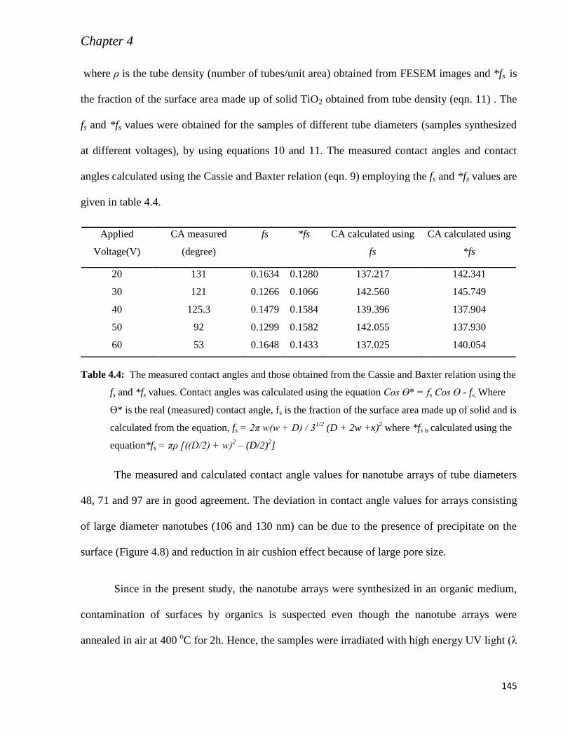
Chapter 4
145
where ρ is the tube density (number of tubes/unit area) obtained from FESEM images and *fs is
the fraction of the surface area made up of solid TiO2 obtained from tube density (eqn. 11) . The
fs and *fs values were obtained for the samples of different tube diameters (samples synthesized
at different voltages), by using equations 10 and 11. The measured contact angles and contact
angles calculated using the Cassie and Baxter relation (eqn. 9) employing the fs and *fs values are
given in table 4.4.
Table 4.4: The measured contact angles and those obtained from the Cassie and Baxter relation using the
fs and *fs values. Contact angles was calculated using the equation Cos * fs Cos - fv, Where
Ө* is the real (measured) contact angle, fs is the fraction of the surface area made up of solid and is
calculated from the equation, fs 2π w(w + D) / 31/2
(D + 2w +x)2 where *fs is calculated using the
equation*fs πρ [((D/2) + w)2 – (D/2)
2]
The measured and calculated contact angle values for nanotube arrays of tube diameters
48, 71 and 97 are in good agreement. The deviation in contact angle values for arrays consisting
of large diameter nanotubes (106 and 130 nm) can be due to the presence of precipitate on the
surface (Figure 4.8) and reduction in air cushion effect because of large pore size.
Since in the present study, the nanotube arrays were synthesized in an organic medium,
contamination of surfaces by organics is suspected even though the nanotube arrays were
annealed in air at 400 oC for 2h. Hence, the samples were irradiated with high energy UV light (λ
Applied
Voltage(V)
CA measured
(degree)
fs *fs CA calculated using
fs
CA calculated using
*fs
20 131 0.1634 0.1280 137.217 142.341
30 121 0.1266 0.1066 142.560 145.749
40 125.3 0.1479 0.1584 139.396 137.904
50 92 0.1299 0.1582 142.055 137.930
60 53 0.1648 0.1433 137.025 140.054

Chapter 4
146
= 250 nm, 1.4 mW/cm2) for 10 h to remove the adsorbed organics responsible for
hydrophobicity, if at all present in trace level. After 10 h of irradiation, the TNTA of different
tube diameters showed superhydrophilicity (contact angle ≤ 5o). The irradiated superhydrophilic
samples were then stored in dark, in a vacuum desicator for weeks, intermittently taking out
samples to measure the water contact angle. The investigations revealed that the initial
hydrophobic state of the N-doped samples was recovered after 30 days. Whereas for the pristine
samples, recovery of hydrophobic state was attained within 16 days. For further studies pristine
and N-doped TNTA synthesized at 40 V and annealed in air at 400 oC for 2 h were chosen. The
rationale behind the selection of samples synthesized at 40 V is that, out of all the samples
synthesized at various voltages, the samples synthesized at 40V have the maximum surface
uniformity and homogeneity in terms of tube diameter, inter tube spacing and tube wall
thickness.
The images of water droplets and variation in contact angle with time left in dark, after
10 hours of UV irradiation, for pristine and N-doped TNTA are shown in Figure 4.9 and 4.10.
The recovery rate calculated from the plots, for the pristine and doped samples are 0.144 and
0.053o per day, respectively. The variation of water contact angles of the pristine and doped
samples were measured with irradiation time till all the samples reached the superhydrophilic
state. Figure 4.11 shows the change in contact angle with UV irradiation time. From figure 4.11
it is clear that both pristine and N-doped samples attained superhydrophilic state in 15 minutes.
The contact angle decay depicts two distinct regimes viz. hydrophobic and hydrophilic. In the
hydrophobic regime the variation is almost linear and change in contact angle is minimum,
whereas it is exponential in the hydrophilic region. The change in contact angle in the
hydrophobic regime is much less pronounced and its variation remains almost linear.

Chapter 4
147
Figure 4.9: Images of water droplets, on pristine and N-doped TNTA, showing increase in contact angle
with time nanotube arrays left in dark.
Figure 4.10: Increase in contact angle with time left in dark (after UV irradiation for 10h), for pristine
and doped samples.
Thereafter it is not considered for kinetics study. The kinetics of the contact angle decay in the
hydrophilic regime can be fitted using an exponential expression.62,88
(12)

Chapter 4
148
The value of the kinetic constant, k, for the contact angle decay under UV irradiation obtained
for pristine and N-doped samples, from the plots (figure 4.11), are 0.57o min
-1 and 0.67
o min
-1
respectively.
Figure 4.11: The variation of contact angle with UV irradiation time for pristine and N-doped TiO2.
After attaining the superhydrophilic state, the samples were kept under dark condition
and contact angles were measured intermittently to study the recovery to the initial hydrophobic
state. The contact angles slowly increased with time, and the pristine and N-doped TNTA
regained its hydrophobic state within 2 and 4 days, respectively. The increase in contact angle
with time kept under dark can be fitted to an exponential function:
(13)
as shown in Figure 4.12. The value of the kinetic recovery constant, krec, obtained from the plot,
for the pristine and N-doped samples are 1.07 x 10⁻³
and 1.01 x 10⁻⁶
min-1
, respectively. The
reversible hydrophobic ↔ superhydrophilic transition was studied several times to establish the
reversible hydrophobic ↔ superhydrophilic switching capability of pristine and N-doped
samples. The observed switching pattern is given in Figure 4.13.

Chapter 4
149
Figure 4.12: The increase in contact angle with time kept under dark after 15 minutes of UV irradiation
for pristine and N-doped TiO2.
Figure 4.13: The reversible hydrophobic ↔ super hydrophilic switching capability of pristine and N-
doped samples under UV/ dark
Since the results of diffuse reflectance spectroscopic studies (chapter 3) indicated visible light
absorption by N-doped samples, the sun light induced hydrophobic – superhydrophilic
transitions and reversible hydrophobic ↔ superhydrophilic switching behavior of N-doped

Chapter 4
150
samples were studied. The N-doped sample attained superhydrophilic nature in 90 minutes of
sun light irradiation and recovered its initial hydrophobicity in two and a half days, when kept in
dark. Figure 4.14 depicts the variation of water contact angle with time of sun light irradiation
and increase in contact angle with time left in dark (after sun light irradiation for 90 minutes),
respectively. The contact angle decay under sun light and recovery with time kept under dark can
be fitted with exponential functions
(14)
(15)
respectively. The value of the kinetic decay constant (ksun) and recovery constant (kdark) obtained
from the plots are 0.06 and 1.01 x 10⁻⁶
min-1
, respectively. Figure 4.15 shows the reversible
hydrophobic ↔ superhydrophilic switching behaviour on exposure to sunlight / dark. The
reversible hydrophobic to superhydrophilic switching behaviour, upon sun light irradiation
followed by storage in the dark, indicate their potential use as visible light active smart
membranes. The mechanism behind the hydrophobic ↔ superhydrophilic switching can be
explained on the basis of the various mechanisms given in the literature. As mentioned in the
introduction, no single mechanism is capable of explaining all the experimental results. Hence, a
combination of mechanisms (photocatalytic decomposition of adsorbed organics and photo
induced surface reconstruction) are considered.89,90

Chapter 4
151
Figure 4.14: (a) the variation of water contact angle with time of sun light irradiation and (b) increase in
contact angle with time left in dark (after sun light irradiation for 90 minutes).
Figure 4.15: The reversible hydrophobic ↔ super hydrophilic switching behavior of N-doped TiO2 on
exposure to sunlight / dark.
In the case of stoichiometric TiO2 and TiO2 with negligible oxide ion vacancies, it is
quite appropriate to state that, the photo generated holes after migrating to the surface take part

Chapter 4
152
in the destruction of adsorbed organics and reaction with oxide ions generating surface O2-
ion
vacancies. The generated oxygen vacancies at the surface take the form of missing oxide ions in
the bridging oxygen row (bridging oxygen vacancies i.e. Ti - VO – Ti) leading to the formation of
coordinatively unsaturated Ti3+
ions. These Ti3+
ions constitute distorted coordination geometry
because of adjacent oxide ion vacancies. These have a tendency to form additional coordination
and therefore, the oxygen vacancies act as adsorption sites for water molecules. The water
molecules adsorbed at the bridging oxygen vacancies are dissociated into OH and H. The OH
group fills the oxygen vacancy to form Ti – OH – Ti / Ti-OH HO-Ti. The surface reconstruction
along with increase in number of the surface OH groups enhances hydrophilicity. In short, upon
irradiation with photons of suitable wave-length, the adsorbed organics are photocatalytically
destroyed and TiO2 surface structure gets reconstructed with increased number of hydroxyl
groups, resulting in hydrophobic to superhydrophilic conversion.
In the case of TiO2 having considerable oxide ion vacancies, for example reduced TiO2
and N-doped TiO2, water dissociatively chemisorbs in the bridging oxygen vacancies creating
hydroxyls, as described above. Hydroxylation at the bridging oxygen vacancies was elucidated
by Wendt et al from the results of scanning tunneling microscopic studies and density functional
theory calculations carried out,91
on reduced rutile TiO2 (110) surfaces which were not subjected
to photo irradiation. That means, in case of reduced or suitably doped TiO2, the surface is already
hydroxylated, and upon irradiating with photons of suitable wave length, the resulting increase in
number of hydroxyl groups and surface reconstruction due to the photo generated holes may not
be the major contributing factor towards the hydrophobic to hydrophilic conversion. A recent
study by Takahashi and Yui on the analysis of OH groups on TiO2 single crystal surfaces (110),
(100) and (001) with polarization modulation infrared external reflection spectroscopy (PM-IER)

Chapter 4
153
did not detect any remarkable increase in the number of surface OH groups to account for the
increase in observed hydrophilicity.80
Based on their results of PM-IER studies on (110), (100)
and (001) surface before, during and after UV irradiation, they explained the photo induced
hydrophilicity owing due to the generation of intermediates such as hydrogen peroxide (H2O2)
and oxonium ions (H3O+), by the photo generated holes and / or electrons, which enhance
hydrogen bonding between adsorbed water molecules, leading to an increase in the amount of
adsorbed water and enhancement of wettability.80
In view of the above discussions, it can be stated that, photocatalytic destruction of
adsorbed organics and the surface reconstruction due to the generation of bridging hydroxyl
groups, and enhancement of hydrogen bonding between the adsorbed water molecules due to the
generation of intermediates such as H2O2 and H3O+ by the photo generated electrons/holes
contribute to the hydrophobic to hydrophilic conversion.
Based on the results of present investigation, it is inferred that in the case of pristine and
N- doped TNTA a combination of the above mentioned mechanisms play a vital role. It is well
understood that, compared to pristine TiO2, N-doped TiO2 samples have higher oxygen vacancy
fraction and hence greater fraction of surface OH group. This was confirmed from the analysis of
the O-1s peak of pristine and N-doped TiO2, obtained from the X-ray photoelectron
spectroscopic studies (Table 4.5). Because of the presence of more number of surface OH
groups, the enhancement in hydrogen bonding between adsorbed water molecules and the
surface hydroxyl groups as well as the bonding between the adsorbed molecules, due the
photogenerated intermediates (H2O2 and H3O+), play a role in the enhancement of wettability and
therefore a low contact angle.

Chapter 4
154
Element Chemical environment
of each element
Binding Energy
(eV)
Doped TiO2
Atom fraction
Pristine TiO2
Atom fraction
O O-Ti(+4)
O-Ti (+3)
HO-Ti(+3,+4)
530.5
530.9
531.9
0.126
0.354
0.152
0.090
0.430
0.113
Ti Ti (+4)-O
Ti (+3)-O
Ti (+3)-OH
Ti (+2)-O
459.4
458.0
456.9
455.6
0.204
0.081
0.032
0.012
0.254
0.062
0.018
0.007
Table 4.5: Atomic fractions of each element in different oxidation states
The plots (Figure 4.11 and Figure 4.14a) representing the contact angle variation with light
irradiation, for the pristine as well as N-doped samples, consist of two regimes viz. a
hydrophobic to hydrophilic and a hydrophilic to superhydrophilic regimes. The first regime can
be ascribed to the effect of surface reconstruction because of the generation of bridging hydroxyl
groups, and enhancement of hydrogen bonding between the adsorbed water molecules. In this
regime the variation of water contact angle with irradiation time is very slow. The second regime
can be ascribed to the effect of photocatalytic organic decontamination (air born pollutants). In
the case of N-doped TNTA because of the presence of more number of surface hydroxyl (Ti-
OH) groups due to doping generated oxygen vacancies, the major contribution towards initial
hydrophilicity can be considered to be from enhancement of hydrogen bonding between the
adsorbed water molecules / water molecules and surface OH groups. The recovery of the initial
hydrophobic state when kept in dark is due to the adsorption of air borne organics and desorption
of intermediate species / molecular water.
4.4. Conclusion
In summary, the solar cell performance of the TNTA on Ti foils and FTO coated glasses
were investigated. The deterioration of the FTO film upon anodization resulted in the incomplete
anodization of Ti thin film and therefore limited length of the nanotubes (~1 micron). In

Chapter 4
155
addition, the annealing of anodized samples at 400 oC deteriorated the film transmittance. A low
fill factor due to improper dye attachment was also observed. These shortcomings limited the
photovoltaic performance of the TNTA on FTO glass. Whereas in the case of TNTA on Ti foils,
the low fill factor, inferior quality of the Pt counter electrode and reduction in light intensity due
to illumination from the counter electrode side contributed to the inferior photovoltaic
performance. Once all these limitation are overcome, it is expected that TNTA will be a
promising candidate material for the third generation solar cells.
The enhancement in electron FE of TNTA with N-doping and variation of electron
emission with concentration of substitutional nitrogen was studied. The emission current was
found to be stable over a duration extending to 5 hours. Systematic variation in electron emission
with increase in N-doping confirms the role played by substitutional nitrogen in FE
enhancement. The enhancement of FE properties on N-doping arises due to the presence of
localized donor states, with higher band width, located at energy levels close to CBM compared
to that of TiO2 and N-2p state above the VBM leading to a shift in Fermi level to higher energies
compared to TiO2.
Nearly superhydrophobic pristine (contact angle = ~140o) and N-doped TNTA (contact
angle = ~125o) were synthesized electrochemically. The hydrophobic to superhydrophilic
conversion of the N-doped nanotube arrays of different tube diameters under UV as well as sun
light were studied and compared with pristine TNTA synthesized under similar conditions. The
doped nanotube array surfaces were more hydrophilic. The hydrophobic to super hydrophilic
conversion was found to be faster for doped samples. Whereas, the time taken for reverting to the
initial hydrophobic state when left in dark was less for pristine TiO2 samples. The results confirm
the superiority of N-doped TiO2 over pristine TiO2 for use as antifogging / self cleaning coatings.
Chapter 4
156
References:
1 Lee, Y.-L.; Lo, Y.-S., Adv. Func. Mater. 2009, 19 (4), 604-609.
2 Adachi, M.; Murata, Y.; Takao, J.; Jiu, J.; Sakamoto, M.; Wang, F., J. Am. Chem. Soc. 2004, 126 (45), 14943-
14949.
3 Mor, G. K.; Shankar, K.; Paulose, M.; Varghese, O. K.; Grimes, C. A., Nano Letters 2006, 6 (2), 215-218.
4 Muduli, S.; Lee, W.; Dhas, V.; Mujawar, S.; Dubey, M.; Vijayamohanan, K.; Han, S.-H.; Ogale, S., ACS App.
Mater. Inter. 2009, 1 (9), 2030-2035.
5 Tan, B.; Wu, Y., J. Phys. Chem. B 2006, 110 (32), 15932-15938.
6 Maggie, P.; Karthik, S.; Oomman, K. V.; Gopal, K. M.; Craig, A. G., J. Phys. D: Appl. Phys. 2006, 39 (12), 2498.
7 Karthik, S.; Gopal, K. M.; Haripriya, E. P.; Sorachon, Y.; Maggie, P.; Oomman, K. V.; Craig, A. G.,
Nanotechnology 2007, 18 (6), 065707.
8 Shankar, K.; Bandara, J.; Paulose, M.; Wietasch, H.; Varghese, O. K.; Mor, G. K.; LaTempa, T. J.; Thelakkat, M.;
Grimes, C. A., Nano Lett. 2008, 8 (6), 1654-1659.
9 Mor, G. K.; Varghese, O. K.; Paulose, M.; Grimes, C. A., Adv. Func. Mater. 2005, 15 (8), 1291-1296.
10 Zheng, H.; Sadek, A. Z.; Breedon, M.; Yao, D.; Latham, K.; Plessis, J. d.; Kalantar-Zadeh, K., Electrochem.
Comm. 2009, 11 (6), 1308-1311.
11 Macak, J. M.; Tsuchiya, H.; Berger, S.; Bauer, S.; Fujimoto, S.; Schmuki, P., Chem. Phys. Lett. 2006, 428 (4–6),
421-425.
12 Varghese, O. K.; Paulose, M.; Grimes, C. A., Nat Nano 2009, 4 (9), 592-597.
13 Kim, J. Y.; Noh, J. H.; Zhu, K.; Halverson, A. F.; Neale, N. R.; Park, S.; Hong, K. S.; Frank, A. J., ACS Nano
2011, 5 (4), 2647-2656.
14 Sadek, A. Z.; Zheng, H.; Latham, K.; Wlodarski, W.; Kalantar-zadeh, K., Langmuir 2008, 25 (1), 509-514.
15 Weickert, J.; Palumbiny, C.; Nedelcu, M.; Bein, T.; Schmidt-Mende, L., Chem. Mater. 2010, 23 (2), 155-162.
16 Nazeeruddin, M. K.; De Angelis, F.; Fantacci, S.; Selloni, A.; Viscardi, G.; Liska, P.; Ito, S.; Takeru, B.; Grätzel,
M., J. Am. Chem. Soc. 2005, 127 (48), 16835-16847.
17 Znamirowski, Z.; Pawlowski, L.; Cichy T.; Czarczynski, W. Surf. Coat. Tech., 2004, 187, 37-46.
18 Fang, X. S.; Bando, Y.; Shen, G. Z.; Ye, C. H.; Gautam, U. K.; Costa, P. M. F. J.;. Zhi, C. Y; Tang C. C.; Golberg,
D. Adv. Mater, 2007, 19, 2593-2596.
19 Huo, K.; Zhang, X.; Fu, J.; Qian, G.; Xin, Y.; Zhu, B.; Ni, H.; Chu, P. K. J. Nanosci. Nanotechnol. , 2009, 9,
3341-3346.
20 Xiang, B.; Zhang, Y.; Wang, Z.; Luo, X. H.; Zhu, Y. W.; Zhang, H. Z.; Yu, D.P. J. Phys. D: Appl. Phys., 2005,
38, 1152-1155.
21 Wu, J. M.; Shih, H. C.; Wu, W. T. Chem. Phys. Lett., 2005, 413, 490-494.
22 Miyauchi, M.; Tokudome, H.; Toda, Y.; Kamiya, T.; Hosono, H. Appl. Phys. Lett., 2006, 89, 43114.
23 Chen, J. B.; Wang, C. W.; Ma, B.H.; Li, Y.; Wang, J.; Guo, R. S.; Liu, W. M. Thin Solid Films, 2009, 517, 4390-
4393.

Chapter 4
157
24
Liu, G.; Li, F. Wang, D. W.; Tang, D. M.; Liu, C.; Ma, X.; Qing Lu, G.; Cheng, H. M. Nanotechnology, 2008, 19,
025606.
25 Raut, N. C.; Mathews, T.; Panda, K.; Sundaravel, B.; Dash S.; Tyagi A. K. RSC Adv, 2012, 2, 812-815.
26 Diwald, O.; Thompson, T. L.; Zubkov, T.; Goralski, E. G.; Walck S. D.; Yates, J. T. J. Phys. Chem. B, 2004, 108,
6004- 6008.
27 Palgrave, R. G.; Payne D. J.; Egdell, R. G. J. Mat. Chem, 2009, 19, 8418-8425.
28 Wang, J.; Tafen, D. N.; Lewis, J. P.; Hong, Z.; Manivannan, A.; Zhi, M.; Li, M.; Wu, N.J. Am. Chem. Soc., 2009,
131, 12290-12297.
29 Valentin, C. D.; Finazzi, E.; Pacchioni, G.; Selloni, A.; Livraghi, S.; Paganini M. C.; Giamello, E. Chemical
Physics, 2007, 339, 44.
30 Oropeza, F. E.; Harmer, J.; Egdell, R. G.; Palgrave, R. G. Phys. Chem. Chem. Phys., 2010, 12, 960-969.
31 Takahashi, I.; Payne, D. J.; Palgrave R. G.; Egdell, R.G. Chem. Phy.s Lett, 2008, 454, 314-317
32 Okato, T.; Sakano T.; Obara, M. Phys. Rev. B., 2005, 72, 115124.
33 Ketteler, G.; Yamamoto, S.; Bluhm, H.; Andersson, K.; Starr, D. E.; Ogletree, D. F.; Ogasawara, H.; Nilsson A.;
Salmeron, M. J. Phys. Chem. C, 2007, 111, 8278-8282.
34 Yim, C. M.; Pang C. L.; Thornton, G. Phys. Rev. Lett., 2010, 104, 036806.
35 Nordheim, L.W. Proc. R. Soc. A, 1928, 121, 626-639.
36 Fowler, R. H.; Nordheim, L. W. Proc. R. soc. A, 1928, 119, 173-181.
37 Das, S.; Ahmed, S.F.; Mitra, M. K.; Chottopadhyay, K. K. Appl. Phys. A: Mater. Sci. Process, 2008, 91, 429-433.
38 Pascual, J.; Camassel, J.; Mathieu, H. Phys. Rev. B, 1978, 18, 5606.
39 Al-Tabbakh, A. A.; More, M. A.; Joag, D. S.; Mulla, I. S.; Pillai, V. K. ACS Nano, 2010, 4, 5585-5590.
40 Nakamura, I.; Negishi, N.; Kutsuna, S.; Ihara, T.; Sugihara S.; Takeuchi, K. J. Mol. Catal. A, 2000, 161, 205-212.
41 Ihara, T.; Ando M.; Suguhara, S. Photocatalysis, 2001, 5, 19 (in Japanese).
42 Justicia, I.; Ordejon, P.; Canto, G.; Mojos, J. L.; Fraxedas, J.; Battiston, G. A.; Gerbasi, R.; Figueras, A. Adv.
Mater., 2002, 14, 1399-1402.
43 Ihara, T.; Miyoshi, M.; Iriyama, Y.; Matsmoto, O.; Sugihara, S. App. Catal. B, 2003, 42, 403-409.
44 Oertzen G.U.; Gerson, A.R. J. Phys. Chem. Solids, 2007, 68, 324-330.
45 Lin, Z.; Orlov, A.; Lambert, R. M.; Payne, M. C. J. Phys. Chem. B, 2005, 109, 20948-20952.
46 Irie, H.; Watanabe, Y.; Hashimoto, K. J. Phys. Chem. B, 2003, 107, 5483-5486.
47 Lindgren, T.; Mwabora, E.; Avendano, J.; Jonsson, J.; Hoel, A.; Granqvist, C.G.; Linduist, S. E. J. Phys. Chem. B
, 2003, 107, 5709-5716.
48 Sakthivel S.; Kisch, H. Chem. Phys. Chem., 2003, 4, 487-490.
49 Irie, H.; Watanabe, S.; Yoshino N.; Hashimoto, K.; Chem. Comm. , 2003, 11, 1298-1299.
50 Valentin, C.D.; Pacchioni, G.; Selloni, A. Phys. Rev. B, 2004, 70, 085116.
51 Nakamura, R.; Tanaka, T.; Nakato, Y. J. Phys. Chem. B, 2004, 108, 10617-10620.
52 Modinos, A. Thermionic and Secondary Electron Emission spectroscopy (Newyork: Plenum) 1984.
53 Murphy E. L.; Good, R. H. Phys. Rev., 1956, 102, 1464.

Chapter 4
158
54
Stratton. R.; Proc. Phys. Soc. B, 1955, 68, 746-757.
55 Morgulis. N.; J. Tech. Phys., 1947, 17, 983.
56 Baskin. L. M.; Lvov. O. I.; Fursey. G. N., phys. stat. sol.(b), 1971, 47, 49-62
57 Linn. S. Q.; Liang. Y. X; Wang. T. H, App. Phys. Lett., 2006, 88, 053107.
58 Drelich, J.; Chibowski, E., Langmuir 2010, 26 (24), 18621-18623.
59Wang, R.; Hashimoto, K.; Fujishima, A.; Chikuni, M.; Kojima, E.; Kitamura, A.; Shimohigoshi, M.; Watanabe, T.,
Nature 1997, 388 (6641), 431-432.
60 Fujishima, A.; Hashimoto K,; Watanabe, T., BKC, Inc: 1999
61 Fujishima, A.; Rao, T. N.; Tryk, D. A., J. Photochem. Photobio. C 2000, 1 (1), 1-21.
62 Stevens, N.; Priest, C. I.; Sedev, R.; Ralston, J., Langmuir 2003, 19 (8), 3272-3275.
63 Wang, R.; Sakai, N.; Fujishima, A.; Watanabe, T.; Hashimoto, K., J.Phys. Chem. B 1999, 103 (12), 2188-2194.
64 Sakai, N.; Wang, R.; Fujishima, A.; Watanabe, T.; Hashimoto, K., Langmuir 1998, 14 (20), 5918-5920.
65 Miyauchi, M.; Nakajima, A.; Fujishima, A.; Hashimoto, K.; Watanabe, T., Chem. Mater. 1999, 12 (1), 3-5.
66 Wang, J.; Mao, B.; Gole, J. L.; Burda, C., Nanoscale 2010, 2 (10), 2257-2261.
67 Daniel, S.; Chaudhury, M. K.; Chen, J. C., Science 2001, 291 (5504), 633-636.
68 Beebe, D. J.; Moore, J. S.; Yu, Q.; Liu, R. H.; Kraft, M. L.; Jo, B.-H.; Devadoss, C., Proceedings of the National
Academy of Sciences 2000, 97 (25), 13488-13493.
69 Zhai, G.-Q.; Ying, L.; Kang, E. T.; Neoh, K. G., Surf. Inter. Anal. 2004, 36 (8), 1048-1051.
70 Samuel, J. D. J. S.; Ruther, P.; Frerichs, H. P.; Lehmann, M.; Paul, O.; Rühe, J., Sensors and Actuators B. 2005,
110 (2), 218-224.
71 Zhang, L.; Dillert, R.; Bahnemann, D.; Vormoor, M., Energy. Environ. Sci. 2012, 5 (6), 7491-7507.
72 Zeman, P.; Takabayashi, S., J. Vac. Sci. Tech. A. 2002, 20 (2), 388-393.
73 Miyauchi, M.; Kieda, N.; Hishita, S.; Mitsuhashi, T.; Nakajima, A.; Watanabe, T.; Hashimoto, K., Surf Sci. 2002,
511 (1–3), 401-407.
74 Zubkov, T.; Stahl, D.; Thompson, T. L.; Panayotov, D.; Diwald, O.; Yates, J. T., J. Phys. Chem. B 2005, 109 (32),
15454-15462.
75 Mills, A.; Crow, M., In Situ, J. Phys. Chem. C 2007, 111 (16), 6009-6016.
76 Sakai, N.; Fujishima, A.; Watanabe, T.; Hashimoto, K., J. Phys. Chem. B 2003, 107 (4), 1028-1035.
77 Sakai, N.; Fukuda, K.; Shibata, T.; Ebina, Y.; Takada, K.; Sasaki, T., J. Phys. Chem. B 2006, 110 (12), 6198-
6203.
78 Hashimoto, K.; Irie, H.; Fujishima, A., Jpn. J. Appl. Phys, 2005, 44, 8269-8285.
79 Watanabe, T.; Nakajima, A.; Wang, R.; Minabe, M.; Koizumi, S.; Fujishima, A.; Hashimoto, K., Thin Solid Films
1999, 351 (1–2), 260-263.
80 Takahashi, K.; Yui, H., J. Phys. Chem. C 2009, 113 (47), 20322-20327.
81 Kontos, A. G.; Kontos, A. I.; Tsoukleris, D. S.; Likodimos, V.; Kunze, J.; Schmuki, P.; Falaras, P.,
Nanotechnology 2009, 20 (4), 045603.
82 Balaur, E.; Macak, J. M.; Tsuchiya, H.; Schmuki, P., J. Mater. Chem. 2005, 15 (42), 4488-4491.
Chapter 4
159
83
Balaur, E.; Macak, J. M.; Taveira, L.; Schmuki, P., Electrochem.y Comm. 2005, 7 (10), 1066-1070.
84 Doohun, K.; Jan, M. M.; Felix, S.-S.; Patrik, S., Nanotechnology 2008, 19 (30), 305710.
85 Wang, J.; Mao, B.; Gole, J. L.; Burda, C., Nanoscale 2010, 2 (10), 2257-2261.
86 Feng, X.; Zhai, J.; Jiang, L., Angew. Chem. Int. Ed. 2005, 44 (32), 5115-5118.
87 Cassie, A. B. D.; Baxter, S., Trans. Farad.Soc. 1944, 40, 546-551.
88 Borrás, A.; López, C.; Rico, V.; Gracia, F.; González-Elipe, A. R.; Richter, E.; Battiston, G.; Gerbasi, R.;
McSporran, N.; Sauthier, G.; György, E.; Figueras, A., J. Phys. Chem. C 2007, 111 (4), 1801-1808.
89 Langlet, M.; Permpoon, S.; Riassetto, D.; Berthomé, G.; Pernot, E.; Joud, J. C., J.Photochem. Photobio. A. 2006,
181 (2–3), 203-214.
90 Yan, X.; Abe, R.; Ohno, T.; Toyofuku, M.; Ohtani, B., Thin Solid Films 2008, 516 (17), 5872-5876.
91 Wendt, S.; Sprunger, P. T.; Lira, E.; Madsen, G. K. H.; Li, Z.; Hansen, J. O.; Matthiesen, J.; Rasmussen, A. B.;
Laegsgaard, E.; Hammer, B.; Besenbacher, F. Science, 2008, 320, 1755-1758.

Chapter 5
160
Chapter 5
Synthesis of Pristine, N and C co-doped TiO2 nanotube powders by Rapid
Break down Anodization Technique and their characterization
Self aligned nanotube arrays are advantageous because of their vectorial electron
conduction compared to nanotube powders. However, in certain applications like hydrogen
generation by photolysis of water, destruction of organics and microbes in water, powders are
advantageous as these can be suspended in the media facilitating better light harvesting
capability and superior reaction kinetics. In addition, the powders can be doctor bladed / screen
printed on to suitable substrates for various applications. The present chapter discusses
electrochemical synthesis of pristine and doped TiO2 nanotubes in the powder form and their
subsequent characterization.

Chapter 5
161
5.1. Introduction
Nanostructured TiO2 is an important candidate material for fabricating functional devices
for various applications in energy and environment. Hence its production in a cost effective,
tunable and easily controllable manner is of scientific and technological interest. Classical
methods to produce nanoporous and nanoparticulates of TiO2 include sol-gel and hydrothermal
synthesis. As detailed in chapter 3 and the references mentioned therein, electrochemical
anodization is an excellent technique to synthesize self aligned TiO2 nanotubes. These self
aligned nanostructures have limitations in photocatalytic applications such as organic
degradation and hydrogen generation where large area exposure is needed for light absorption
and reactant adsorption. Therefore, nanotubes in the powder form, which can be dispersed in the
medium containing the reactants, are generally preferred. It is a common practice to synthesize
self aligned TiO2 nanotubes by anodizing Ti in fluoride ion containing electrolytic medium.
Extending this synthesis method in chloride ion containing medium, Hahn et al synthesized
nanotube powders of TiO2 and WO3 in sodium per chlorate and perchloric acid media.1 In 2009,
Fahim and Sekino synthesized nanotubes of TiO2 in powder form by electrochemical anodization
technique using Ti foils in perchloric acid and sodium chloride / sodium phosphate media and
this electrochemical approach was termed as rapid break down anodization technique.2 They
obtained X-ray amorphous TiO2 nanotube powders, which on heating crystallized into anatase
phase in a temperature range 300 – 500 oC. Heating beyond 500
oC resulted in anatase to rutile
phase transformation.
It has been reported recently that the visible light activity of TiO2 can be enhanced by
nitrogen doping which is already explained in chapter 3. The enhancement in photocatalytic
activity can be further improved by C and N co-doping.3-5
Chen et al reported that TiO2 shows an
Chapter 5
162
efficient photocatalytic activity by substitutional doping of carbon and nitrogen in the oxygen
lattice. The carbonaceous species formed at the TiO2 surface during C-doping are potential sites
for adsorption of organic molecules.
The present study describes the synthesis of high surface area TiO2 nanotube powders,
having wall thickness, pore diameter as well as particle size less than those reported by Fahim
and Sekino2. In this study anatase - TiO2 nanotube powders were obtained in as prepared state.
Anodization was carried out at 10 and 20 V in perchloric acid medium at room temperature.
Structure, morphology and optical properties of the as prepared and annealed samples as well as
the annealing temperature limit for maintaining the tubular morphology and phase purity were
investigated. Further, synthesis of C and N- co-doped anatase TiO2 nanotube powders were
carried out by anodizing Ti foil in a highly oxidative electrolyte (0.1 M HClO4) containing urea
as C and N source.
5.2. Experimental details
5.2.1 Synthesis of TiO2 nanotube powders
Preparation of electrodes (Ti and Pt) was carried out according to the procedures
mentioned in chapter 3. Reagent grade perchloric acid was chosen as the electrolyte. The
titanium foils and the platinum cathode were connected to electrical leads by means of crocodile
clips and dipped into the electrolyte solution (0.1 M perchloric acid). Two anodization
experiments, one at room temperature (10 and 20V) and the other at 2 o
C (20V) were carried
out. The variation of current with time, during anodization, was recorded using a computer
controlled digital multimeter. Anodization was continued until the Ti foil completely
transformed into TiO2 powder. The white powders obtained after anodization at 10 V (26 oC),

Chapter 5
163
20 V (26 oC) and 20 V (2
oC) were named as NP1, NP2 and NP3, respectively. These powders
were washed several times with de-ionized water, centrifuged and dried overnight at 50 oC in a
Petri dish. The samples were then annealed at 400, 500, 600 and 700 oC, at a heating rate of 3
o
per minute, for two hours and then cooled slowly. For the synthesis of C and N co-doped TiO2
nanotube powders Ti foils are anodized in 0.1 M perchloric acid containing 3.75 wt% urea.
These powders were washed several times with double distilled water, centrifuged and kept in a
Petri dish over night for drying. The undoped and doped TiO2 samples were analyzed using
different microscopic and solid state characterization techniques.
5.2.2. Characterization
Field Emission Scanning Electron Microscopic, XRD, micro Raman, Diffuse reflectance,
XPS analyses of the pristine and doped TiO2 nanotube powders were carried out as described in
chapter 2. The surface areas of the samples were measured by Brunauer Emmet Teller (BET)
adsorption method (Sorptomatic 1990, Thermo Electron Corporation, US), using nitrogen gas as
an adsorbate. The transmission electron microscopic (TEM) analyses of the samples were carried
out TEM equipment, make Philips, Netherlands. The samples for TEM studies were prepared by
placing a drop of nanotube powder suspension in methanol on a carbon coated copper grid and
allowing it to dry. The crystal structure of the nanotube powders were obtained from Selected
Area Electron Diffraction (SAED) pattern. The photoluminescence (PL) measurements were
carried out using the Jobin Yvon-Spex make Spectrofluorometer (Fluorolog version-3; Model
FL3-11) with 450 W high pressure xenon arc lamp as an excitation source. PL excitation and
emission spectra were acquired at room temperature for a spectral resolution of 0.2 nm and slit
width of 0.25 mm.

Chapter 5
164
5.3. Results and Discussions
5.3.1. Synthesis and characterization of Pristine TiO2 nanotube powders
5.3.1.1. Potentiostatic transient and nanotube formation
The variation of current with time during the electrochemical processes is shown in Figure
5.1. During initial stages of anodization, formation of a white layer of titanium dioxide was
observed on the surface of the Ti metal, which started breaking down into the electrolytic
solution as white powders. The anodization reaction can be represented as
2Ti + 2H2O 2TiO2 + 4e + 4H+ (1)
The rate of oxide formation is faster in the initial stage. The initial white TiO2 layer formed on
the metal surface started dissolving because of electrochemical etching by chlorine species
giving rise to the formation of pits. The subsequent inward migration of oxide ions resulted in
the formation of a thick porous layer of TiO2 leading to reduction in current. In addition, the
chlorine species etched the Ti metal causing dissolution of Ti as [TiCl6]2-
. The electrochemical
etching of Ti metal facilitated the easy breakdown of the oxide layer. Because of the high
mechanical stress existing between the metal and metal oxide interface, originating from
mismatch in crystal volume, a small disturbance is good enough to remove the metal oxide layer.
This disturbance was provided by chemical reactions in the electrolyte, strong bubbling in the
solution due to hydrogen evolution at the cathode and local turbulence arising from magnetic
stirring of the solution. The periodic release of oxide layer continued until the complete
conversion of Ti metal to TiO2. The current – time profile of the room temperature anodization
performed at 10 and 20 V (Figure 5.1) are similar except for the current magnitude and time
duration at each stage. The differences can be attributed to the change in kinetics with applied
potential. During room temperature anodization at 20 V, the electrolyte bath temperature

Chapter 5
165
increased by ~15-18 oC whereas, the rise in temperature was only ~3
oC at 10 V. The relatively
large rise in temperature, at 20 V, led to increase in current. In addition, the breakdown of
titanium oxide layer started within minutes of anodization exposing fresh metal surface, whereas
the onset as well as rate of oxide layer breakdown was slow at 10 V.
Figure 5.1: Variation of current with time during anodization
In the case where applied voltage and electrolyte temperature were 20 V and ~2 oC,
respectively, the current increased slowly and then decreased very slowly until the Ti metal was
completely oxidized to TiO2. The slow change in current with time is because of the slow
reaction kinetics at low temperature. The surface area of the sample calculated from BET
adsorption plot is 155 g/m2.
5.3.1.2. Field emission scanning electron microscopic studies
The FESEM images of the TiO2 powder samples NP1, NP2 and NP3 are shown in Figure
5.2. The images reveal clusters of nanotubes of high aspect ratio. The SEM images indicate that
changes in the experimental conditions did not change the morphology but the growth rate.
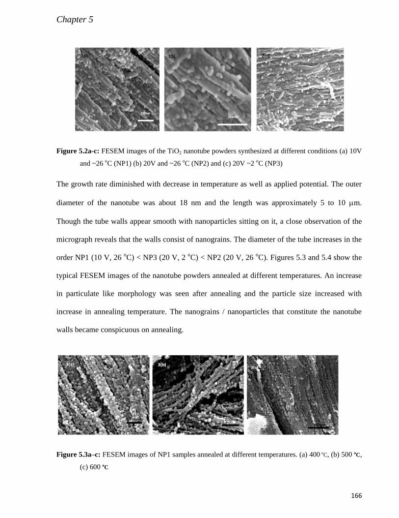
Chapter 5
166
Figure 5.2a-c: FESEM images of the TiO2 nanotube powders synthesized at different conditions (a) 10V
and ~26 oC (NP1) (b) 20V and ~26
oC (NP2) and (c) 20V ~2
oC (NP3)
The growth rate diminished with decrease in temperature as well as applied potential. The outer
diameter of the nanotube was about 18 nm and the length was approximately 5 to 10 m.
Though the tube walls appear smooth with nanoparticles sitting on it, a close observation of the
micrograph reveals that the walls consist of nanograins. The diameter of the tube increases in the
order NP1 (10 V, 26 oC) < NP3 (20 V, 2
oC) < NP2 (20 V, 26
oC). Figures 5.3 and 5.4 show the
typical FESEM images of the nanotube powders annealed at different temperatures. An increase
in particulate like morphology was seen after annealing and the particle size increased with
increase in annealing temperature. The nanograins / nanoparticles that constitute the nanotube
walls became conspicuous on annealing.
Figure 5.3a–c: FESEM images of NP1 samples annealed at different temperatures. (a) 400 oC, (b) 500 oC,
(c) 600 oC

Chapter 5
167
Figure 5.4a–c: FESEM images of NP1, NP2 and NP3 samples annealed at 700 oC.
The SEM images of the samples (NP1) annealed at 400 oC and 500
oC reveals that the
overall morphology of the samples is retained, although the nanograins which constitute the tube
walls are clearly visible (Figure 5.3a and 5.3b). The SEM image of the samples (NP1) annealed
at 600 oC shows that the nanotubes start to disintegrate to particles resulting in a morphology
having both nanotubes and nanoparticles (Figure 5.3c). Similar features are seen in the case of
NP2 and NP3 samples annealed at 400, 500 and 600 oC. Figure 4 depicts the SEM images of the
samples (NP1, NP2, NP3) annealed at 700 oC. An increase in disintegration of tubular
morphology in the ascending order NP1 < NP2 ≤ NP3 is discernible.
5.3.1.3. Transmission electron Microscopic studies
The TEM image of the as prepared sample (NP1) revealing the tubular microstructure of the
powders is shown in figure 5.5a. The tubes are of uniform width measuring about 15 to 18 nm in
diameter. The inner diameter of the tubes varies from 5 to 8 nm and the wall thickness is about 5
nm. Similar images were obtained for NP2 and NP3 samples. Figure 5.5b shows the SAED
pattern of sample NP1, the different (hkl) planes were identified as (101), (103), (105), (204) and
(116) of anatase phase. TEM studies were also carried out for the annealed samples of nanotube
powders synthesized at 10V (NP1). The tubular nature as observed in the case of as prepared
samples were not clearly seen in the case of annealed samples.

Chapter 5
168
Figure 5.5a-b: (a) TEM image of the TiO2 nanotube powders synthesized at 10V (~26º C). (b) SAED
pattern of NP1 (as prepared)
Figure 5.6a–b: TEM images (a) NP1 annealed at 600 oC (b) NP1 annealed at 700
oC (shows complete
destruction of tubular morphology). Figure 6b: SAED pattern of the NP1 annealed at 700 oC
The TEM image of sample annealed at 600 oC (Figure 5.6a) shows linear array of
nanograins indicating tube collapse. At 700 oC, the tubular morphology is completely lost
resulting in the formation of nanograins distributed in random, as shown in Figure 5.6b. The
results obtained from the TEM results are in agreement with the SEM observations. The SAED

Chapter 5
169
pattern (Figure 5.6c) of the sample annealed at 700 oC reveals that the sample is comprised of
rutile phase in agreement with the XRD results given below.
5.3.1.4. Powder X-ray diffraction studies
The crystalline nature of the as prepared samples is further confirmed by XRD. Figure
5.7 depict the XRD pattern of the as prepared samples. The pattern matches well with that of
anatase phase. The presence of broad peaks indicates that the crystallite size is in the nanometer
regime. The crystallite size calculated for the samples NP1, NP2 and NP3, using Scherer
formula, are 10, 13 and 12 nm, respectively. The microscopic and XRD studies confirm the
formation of anatase phase of nanotube powders by electrochemical synthesis, without any
additional post annealing requirement. The XRD patterns of the as prepared and annealed NP1
samples are shown in Figure 5.8. From the XRD patterns, it is clear that the anatase phase is
Figure 5.7: XRD pattern of the as prepared samples (NP1, NP2 and NP3)
stable up to a temperature of 500 oC. XRD pattern of the sample annealed at 600
oC shows the
presence of both rutile and anatase phases. At 700 oC complete transformation to rutile phase
occurs. Figure 5.9 shows the variation of crystallite size with annealing temperature.
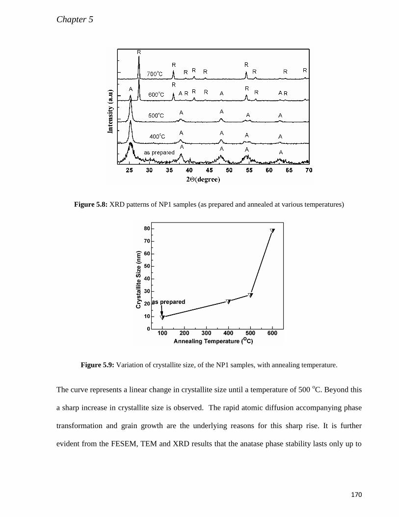
Chapter 5
170
Figure 5.8: XRD patterns of NP1 samples (as prepared and annealed at various temperatures)
Figure 5.9: Variation of crystallite size, of the NP1 samples, with annealing temperature.
The curve represents a linear change in crystallite size until a temperature of 500 oC. Beyond this
a sharp increase in crystallite size is observed. The rapid atomic diffusion accompanying phase
transformation and grain growth are the underlying reasons for this sharp rise. It is further
evident from the FESEM, TEM and XRD results that the anatase phase stability lasts only up to

Chapter 5
171
500 oC. These results indicate that from application point of view where the anatase-TiO2 is more
efficient, the sample should preferably be annealed below 500 oC.
5.3.1.5. Raman Spectroscopy analysis
Figure 5.10 shows the Raman spectra of the as prepared TiO2 nanotube powders. The
crystal structure of anatase-TiO2 is tetragonal (space group D19
4h (I41/amd)) with two TiO2
formula molecular units in the primitive cell giving rise to six Raman active phonons in the
vibrational spectra: three Eg (144, 197 and 639 cm-1
), two B1g (399 and 519 cm-1
) and one A1g
(513 cm-1
). For rutile TiO2 there are four active modes: 144 cm-1
(B1g), 448 cm-1
(Eg), 613 cm-1
(A1g) and 827 cm-1
(B2g).6-8
Four peaks appear at around 149, 396, 517 and 638 cm-1
and these
peaks are assigned to Eg, B1g, B1g/A1g and Eg modes, respectively. The intense low frequency
band at 149 cm-1
arises from the O – Ti - O bending vibrations and is a characteristic feature of
the anatase phase of TiO2. All the four peaks correspond to the Raman active phonon modes of
tetragonal anatase phase of TiO2.6 It can be seen that the intense Raman peak corresponding to
the Eg mode of TiO2 (144cm-1
for standard bulk samples) has shifted towards higher wave
number and the FWHM is high compared to those of standard microcrystalline samples. The
shift and broadening of the Raman peaks observed in this study suggest the presence of size
effects and can be attributed to the optical phonon confinement effect in agreement with the
literature where quantum confinement effect in TiO2 nanoparticles giving rise to blue shift is
reported.9,10
The broadening of Raman line can be attributed to gross structural disorder in
nanocrystalline phase. The peak positions and FWHM of the Raman peaks of the as prepared
samples (NP1, NP2 and NP3), obtained by fitting to Lorenzian, are shown in Table 5.1. In
addition to the shift and broadening an asymmetry is seen on the peak (149 cm-1
) which can be
attributed to the contribution from the less intense Raman peak at 197 cm-1
(Eg). No other peaks

Chapter 5
172
corresponding to rutile or any other TiO2 polymorphs are seen in the spectra, which is in good
agreement with XRD results.
Figure 5.10: Raman spectra of the as prepared samples (NP1, NP2 and NP3).
Sample Eg (cm-1
) B1g (cm-1
) A1g +B1g(cm-1
) Eg (cm-1
)
10V (26 K)/ NP1 153.05(30.59) 401.83(40.06) 514.51(86.18) 639.68(111.59)
20V (26 K) / NP2 149.11(23.04) 398.95(31.23) 516.13(10.59) 639.49(76.04)
20V (2 K) / NP3 153.12(38.97) 401.74(40.98) 516.62(38.97) 639.34(52.32)
Table 5.1: The wave number and the FWHM (in parentheses) of Raman spectra of the samples
5.3.1.6. Photoluminescence studies
The photoluminescence spectroscopy is a useful technique to reveal the efficiency of
charge carrier trapping and transfer in semiconducting materials.11
Figure 5.11 shows the PL
spectra of the as prepared and annealed NP1 samples. Broad, asymmetric PL bands, tailing
towards low photon energies and peaking around 3.1 eV and 3.0 eV are observed for NP1 as
well as NP1 annealed at 400 oC and 500
oC and for NP1 annealed at 600
oC and 700
oC,
respectively. The band gaps of the samples evaluated from the peak positions of the PL spectra

Chapter 5
173
as fitted to Gaussian are 3.12, 3.13, 3.13, 3.02, and 3.01 for NP1, NP1 annealed at 400 oC, 500
oC, 600
oC and 700
oC respectively. The spectra on deconvolution revealed the presence of three
main PL bands. The bands around 3.1 eV (in the case of NP1, NP1 annealed at 400 oC and 500
oC) and 3.0 eV (NP1 annealed at 600
oC and 700
oC) are attributed to the indirect transitions.
For TiO2 nanotubes, because of high surface to volume ratio, substantial number of Ti
ions are exposed at the surface. As evident from FTIR studies, sufficient numbers of these atoms
exist as O-Ti-OH. The presence of Ti-OH bonds distort the TiO6 octahedra and introduce
localized energy states within the band gap. These charge-carrier trapping surface states with
different energy levels become luminescent centers. The PL bands observed around 2.85 eV and
the flat bands around 2.65 eV (440 to 480 nm) with several sharp peaks can be ascribed to
luminescence from these surface states that are present on the distorted TiO6 octahedra (excitons
trapped at shallow-trap and medium-trap surface states). It is seen from the spectra that the PL
intensity increases as the sample is annealed at 400 oC and then starts decreasing on annealing at
500oC. The temperature dependence of the PL data may be attributed to the different structural
phases and microstructures of the annealed samples. The rise in PL intensity (at 400 oC) can be
attributed to annealing of defects and thereby causing scattering elimination if scattering centers
are present in the as prepared sample. The rise in intensity is also accompanied with the
reduction in the FWHM signifying reduction in disorder. Further increase in annealing
temperature to 500 oC causes reduction in spectral intensity. The PL spectra of the as prepared
and annealed samples (400 and 500 oC) are very similar except for the small difference in
intensity. Whereas the spectra of the samples annealed at 600 and 700 oC are different and are
accompanied with enhanced broadening, decrease in spectral symmetry and intensity. This is
because the as prepared and 400 and 500 oC annealed samples are of anatase phase whereas the

Chapter 5
174
600 oC annealed sample is a mixture of anatase and rutile phases and the sample annealed at 700
oC is completely
Figure 5.11: Photoluminescence spectra of the annealed samples of NP1
rutile. The presence of rutile phase enhances the broadening and reduces the PL intensity
because of its poorer photo-reactivity compared to anatase. The observed gradual red shift
indicates anatase to rutile phase transformation in agreement with the XRD and SAED results.
The red shift observed in the case of NP1 annealed at 600 oC (mixture of rutile and anatase) is
induced by charge transfer from anatase to rutile. As the conduction band energy level of anatase
is higher than that of rutile some electrons in the anatase particles that are excited from the
valence band to the conduction band transfer to the conduction band of rutile, and the photo-
induced electrons and holes recombine to give luminescence.

Chapter 5
175
5.3.1.7. Optical Characterization
The optical absorption studies were carried out by taking the diffuse reflectance spectra
of the powder samples. The optical band gap, obtained by extending the line, from the slope of
the linear part of the Tauc plot, to x = 0, is 3.07, 3.05 and 2.95 eV for NP1, NP2 and NP3,
respectively. Whereas the band gap reported in the literature for anatase TiO2 is 3.2 eV. The
reflectance spectra and the Tauc plot of the as prepared samples are depicted in Figures 5.12a
and 5.12b respectively. Similar plots were obtained for NP1 samples annealed at different
temperatures and the band gap values evaluated from the plots are given in Table 5.2. In the case
of NP1 samples annealed at different temperatures, there is a declining trend in band gap with
increase in annealing temperature. This reflects anatase to rutile phase transformation. The lower
band gap of the rutile phase makes the absorption edge appear around visible region. The
decrease in band gap values of the nanotubes compared to those reported can be attributed to the
presence of oxygen vacancies. The broad peak in the PL spectra also gives evidence of oxygen
vacancies, which creates a decrease in the band to band transition energy. Band gaps obtained
from both PL and DRS studies are given in table 5.2. The mechanism of absorption of light in
semiconducting materials involves the use of photon energy to excite the electrons from valence
band to the conduction band. In the present case, the absorption is in the visible range close to
UV. Therefore, the TiO2 nanotubes could find active use in photocatalytic applications.

Chapter 5
176
Figure 5.12a-b: (a) Diffuse reflectance spectra of the as prepared samples (NP1, NP2 and NP3), (b) Tauc
plot of the as prepared samples (NP1, NP2 and NP3). The band gaps are 3.07, 3.05 and 2.95 for
NP1, NP2 and NP3 samples respectively.
Sample Details Band gap (Eg) calculated from
PL(eV)
Band gap (Eg) calculated from
DRS(eV)
NP1 3.12 3.07
NP2 - 3.05
NP3 - 2.95
annealedNP1(400 oC) 3.13 2.85
annealedNP1(500 oC) 3.13 2.91
annealedNP1(600 oC) 3.02 2.87
annealedNP1(700 oC) 3.01 2.88
Table 5.2: Band gap of the TiO2 nanotubes obtained from photo luminescent and diffuse reflectance
studies
5.3.1.8. Fourier transform infrared spectroscopic analysis
The FTIR spectra of the as prepared sample NP1 as well as the annealed NP1 samples are
shown in Figure 5.13. The spectra show strong absorption bands at 3200-3600 and 1630 cm-1
, for
the as prepared samples. These are attributable to the stretching mode of the OH group and the
deformation mode of the molecular water, respectively. This characteristic mode reveals that
there are chemisorbed as well as physisorbed hydroxyl species on the surface of TiO2

Chapter 5
177
nanotubes.12
The same features were present in the FTIR spectra of the samples annealed at 400
and 500 oC.
Figure 5.13: FTIR spectra of the NP1 samples annealed at various temperatures
However, in the case of samples annealed at 600 and 700 o
C the characteristic vibrational modes
corresponding to the OH groups were absent. There is an additional broad band over the range of
400-800 cm-1
that corresponds to the characteristic peak of TiO6 octahedra.13,14
As the annealing
temperature increases this band becomes sharper suggesting that the Ti-OH bonds converts to a
strong network of Ti-O-Ti in TiO2 framework. The present data obtained agrees well with the
reported values.12,15

Chapter 5
178
5.3.2. Synthesis and characterization of N & C co-doped TiO2 nanotube
powders
5.3.2.1. Synthesis
The current density variation with time during anodization of Ti foil in 0.1 M HClO4 and
0.1 M HClO4 + urea is shown in Figure 5.14. The observed transients are similar confirming
similar mechanism as described in earlier section.
Figure 5.14: Potentiostatic transients during anodization.
5.3.2.2. Scanning and Transmission Electron Microscopic Analysis
The morphology of the samples synthesized in urea containing electrolyte were
investigated by FESEM and TEM. The micrographs obtained are given in Figure 5.15. The
nanotubular morphology observed in the case of samples synthesized in electrolyte without urea
could not be seen in the case of samples synthesized in urea containing electrolyte.
Disintegration of tubular morphology could be discerned from the SEM (Figure 5.15a) and TEM
images (Figure 5.15b).

Chapter 5
179
Figure 5.15a-b: (a) FESEM images of doped TiO2 nanotube powders, (b) TEM images of doped TiO2
nanotube powders
5.3.2.3. X-ray photoelectron spectroscopic studies
Since urea was used as a precursor for doping C and / N- doping was expected. Hence the
N1s and C1s high resolution photoelectron spectra of the doped samples were taken and
analyzed in detail. Figure 5.16 shows the N 1s spectrum corresponding to doped TiO2. The
deconvoluted N 1s spectrum shows peaks at 404.62, 402.76, 401.10 and 399.79 eV. In the
present study, no peaks were observed, at ~397 eV, corresponding to N-Ti-O, indicating absence
of oxygen substitution by nitrogen in the oxygen sub-lattice. The peak at 399.79 eV is assigned
to the interstitial nitrogen ie; Ti-O-N type of chemical linkage. Figure 5.17 shows the C 1s
deconvoluted spectrum of doped TiO2. The deconvoluted C1s spectra reveal five peaks
positioned at 289.25, 286.53, 284.96, 281.79 and 280 eV. The peak at 284.96 eV indicates
presence of adventitious carbon. The peaks corresponding to 281.79 and 280 eV can be assigned
to carbon in the oxygen sub-lattice (C-Ti-O). The peaks at 289.53 and 286.53 eV belong to Ti
(CO3)2 and Ti (CO3)n, because the carbon atom diffuses through the Ti matrix and substitute the
Ti or occupies the interstices in the lattice.16
The above results indicate formation of C and N- co

Chapter 5
180
doped TiO2 nanotubes, where nitrogen occupies the interstitial position resulting in the formation
of Ti-O-N bond species and carbon substitutes oxygen in the oxygen sub-lattice.
Figure 5.16: High resolution N 1s spectra of the doped TiO2 sample.
Figure 5.17: High resolution C 1s spectra of the doped TiO2 sample.
5.3.2.4. X-ray Diffraction Studies
The XRD pattern of the sample is given in Figure 5.18. The XRD pattern of the pristine

Chapter 5
181
sample is also shown for comparison. The pattern matches well with that of anatase phase. No
peaks corresponding to rutile TiO2 are observed. The presences of broad peaks indicate that the
crystallite sizes are in the nanometer regime. No changes in d spacing (101), could be observed.
Thus doping does not change the crystallinity of the TiO2 and is consistent with the earlier
reports.3,4,5
The crystallite sizes of the pristine and doped samples were calculated from the
Scherrer formula. It was observed that the crystallite size of TiO2 has increased from 10 to 13 nm
when the doping was carried out. This change is also reflected in the BET surface area of the
doped samples. The surface area decreased with doping (155 m2/g to 124 m
2/g).
Figure 5.18: XRD patterns of undoped and doped TiO2 nanotubes
5.3.2.5. Optical Characterization
The diffuse reflectance spectra of the powders are shown in Figure 5.19a. The reflectance
spectra of the undoped samples are also shown for comparison. From the reflectance spectra of
the samples (Figure 5.19a), it is clear that there is a small red shift in the absorbance of the doped
TiO2 sample. Figure 5.19b represents the variation of (F*E)1/2
against E. The observed band gap

Chapter 5
182
from the Tauc plot (Figure 5.19b) for pristine and doped TiO2 samples are 3.1 eV and 3.06 eV,
respectively. The observed is very small red shift and lies within the error within limit.
Figure 5.19a-b: (a) Diffuse Reflectance plots of the undoped and doped TiO2 nanotubes, (b) Tauc plot of
the undoped and doped TiO2 nanotubes
Figure 5.20a shows the PL spectra of the doped samples (PL spectra of the pristine
samples are given for comparison). The spectra on deconvolution revealed the presence of three
main PL bands. The main peak around 3.10 eV for doped TiO2 samples is attributed to the
indirect transition. The PL bands observed around 2.80 eV and 2.19 eV can be ascribed to
luminescence arising from the surface states that are present on the distorted TiO6 octahedra
(excitons trapped at shallow-trap and medium-trap surface states). The rise in PL intensity in the
case of doped TiO2 can be attributed to the higher density of defects. These defects state can act
as the electron-hole recombination centres, thereby reducing the photocatalytic efficiency. Figure
5.20b shows the Raman spectra of pristine (shown for comparison) as well as doped TiO2. In the
case of doped TiO2, in addition to the 7 bands, a band at 859.91 cm-1
is observed. Compared to
the peak positions of pristine TiO2, the peaks of doped TiO2 are shifted to higher wave numbers.

Chapter 5
183
Figure 5.20a-b: (a) Photoluminescence spectra of the undoped and doped TiO2 nanotubes, (b) micro
Raman spectra of the undoped and doped TiO2 nanotubes.
The Raman features at 149.71, 204.1, 515.67 and 630.33 can be attributed to the Eg, Eg, B1g and
Eg vibrational modes of anatase phase, respectively. An additional peak at 859.91cm-1
is assigned
to the B2g mode of rutile and can be attributed to the presence of rutile phase in the doped
samples. So the sample contains a very low percent of rutile phase which could not be resolved
in X-ray diffraction pattern. Similar observations are reported by Okato et al., where interstitial
N- doping hindered the growth of anatase phase, giving rise to evolution of rutile phase.17
From the results of diffuse reflectance and PL studies, it is clear that there is no significant
difference between the band structures of pristine and doped TiO2, even though presence of
substitutional carbon and interstitial nitrogen could be discerned from the XPS results. Hence, an
enhancement in photocatalytic properties cannot be expected. In turn, deterioration in
photocatalytic property is possible due to the generation of defect states, arising upon doping,
which acts as electron-hole recombination centres. Indeed, this has been observed and is
presented in the succeeding chapter.

Chapter 5
184
5.4. Conclusion
High aspect ratio anatase phase TiO2 nanotube powders were synthesized by employing
rapid breakdown anodization technique. The method is simple, cost effective and easy. The
yields of the TiO2 nanotube powders were high as compared with other synthesis techniques.
Even though potentiostatic anodization was employed, the transient was completely different
from the expected one. This may be attributed to the periodic release of the TiO2 formed on
surface. Change in the applied potential and temperature did not have much effect on the sample
morphology. However, the growth rate variation was noticed while changing experimental
condition. The asprepared powders were confirmed to have tubular morphology with ~8 nm
inner diameter and ~5 nm wall thickness as revealed from FESEM and TEM analysis. The
SAED, XRD and Raman spectral studies revealed that these nanotubes are polycrystalline and is
of anatase phase having crystallite size varying from 9 to 13 nm. The morphology and phase
changes of the samples annealed at different temperatures, revealed by various techniques,
enabled fixing of annealing temperature to confine to a specific morphology and phase,
depending on the type of application. The photoluminescence of the nanotube powders have
shown a temperature dependence that can be attributed to the change in crystallinity and
microstructure which occurs with variation in annealing temperature. The as prepared samples
showed good optical properties, where the band gaps varied from 2.95 to 3.07 eV. Compared to
TNTA, even though self organized property of the material was lost in the present case, the
nanotubes were of smaller diameter and wall thickness, and exhibited quantum confinement
effects. While the TNTA are amorphous, as is the case in the asprepared condition, the nanotube
powders consist of anatase phase. Simultaneous C and N-doping was attempted using urea in the
electrolyte as precursor for C and N. XPS analysis revealed the incorporation of nitrogen into the

Chapter 5
185
TiO2 matrix as interstitials and carbon substituting oxygen in the anion sub-lattice. XRD and
TEM analysis revealed the samples to be of anatase phase and 12 nm – 14 nm crystallite sizes.
Diffuse reflectance measurements revealed very small red shift of 0.04 eV in the band gap of
doped TiO2 indicating no significant reduction in the band gap.

Chapter 5
186
References
1 Hahn, R.; Macak, J. M.; Schmuki, P., Electrochem. Comm. 2007, 9 (5), 947-952.
2 Fahim, N. F.; Sekino, T., Chem.Mater. 2009, 21 (9), 1967-1979.
3 Chen, D.; Jiang, Z.; Geng, J.; Wang, Q.; Yang, D., Indus. Eng. Chem. Res. 2007, 46 (9), 2741-2746.
4 Zhou, A.; Wang, X.; Qu, J.; Wang, Y.; Li, Y.; Wang, G., Adv. Mater. Res., 2011, 148-149, 1007-1010.
5 Yin, S.; Komatsu, M.; Zhang, Q.; Saito, F.; Sato, T., J. Mater. Sci. 2007, 42 (7), 2399-2404.
6 Hu, M.; Lai, P.; Bhuiyan, M.; Tsouris, C.; Gu, B.; Parans Paranthaman, M.; Gabitto, J.; Harrison, L., J. Mater. Sci.
2009, 44 (11), 2820-2827.
7 Ohsaka, T.; Izumi, F.; Fujiki, Y., J. Raman Spec. 1978, 7 (6), 321-324.
8 Tang, H.; Prasad, K.; Sanjines, R.; Schmid, P. E.; Levy, F., J. App. Phys. 1994, 75 (4), 2042-2047.
9 Xu, C. Y.; Zhang, P. X.; Yan, L., J. Raman Spec.y 2001, 32 (10), 862-865.
10 Pottier, A.; Cassaignon, S.; Chaneac, C.; Villain, F.; Tronc, E.; Jolivet, J.-P., J. Mater. Chem. 2003, 13 (4), 877-
882.
11 Li, X. Z.; Li, F. B.; Yang, C. L.; Ge, W. K., J.Photochem. Photobiol. A. 2001, 141 (2–3), 209-217.
12 Jensen, H.; Soloviev, A.; Li, Z.; Søgaard, E. G., App. Surf. Sci. 2005, 246 (1–3), 239-249.
13 Zeitler, V. A.; Brown, C. A., J.Phys. Chem. 1957, 61 (9), 1174-1177.
14 Mauritz, K. A.; Jones, C. K., Kumar, P. M.; Badrinarayanan, S.; Sastry, M., Thin Solid Films 2000, 358 (1–2),
122-130.
15 Mauritz, K. A.; Jones, C. K., J. App. Polym. Sci. 1990, 40 (7-8), 1401-1420.
16 Rengifo-Herrera, J. A.; Mielczarski, E.; Mielczarski, J.; Castillo, N. C.; Kiwi, J.; Pulgarin, C., App. Catal. B.
2008, 84 (3–4), 448-456.
17 Okato, T.; Sakano, T.; Obara, M., Phys. Rev. B 2005, 72 (11), 115124.

Chapter 6
187
Chapter 6
Photocatalytic Hydrogen generation and dye degradation studies using
Pristine and C and N co-doped TiO2 nanotube powders
Various nano-architectures of TiO2, with tailored geometry having high surface area are
being studied for various functional applications in energy and environment. In applications like
green-energy hydrogen generation by splitting of water and photocatalytic decomposition of
organic pollutants in water, suspensions of large surface area particles like nanotubes are
preferred as the configuration has better light harvesting capability and hence superior
efficiency. The present chapter deals with the studies on hydrogen generation by photo assisted
water splitting using Pt loaded TiO2 nanotubes suspended in water-organic mixture and photo-
assisted destruction of organics in water by pristine and C and N co-doped TiO2 nanotube
powder suspensions in water.

Chapter 6
188
6.1. Introduction
Presently, the major source of energy for industrial and economic purposes is fossil fuels.
Depletion of fossil fuel reserves and pollution caused by combustion of fossil fuels is a major
concern. Hydrogen, an effective energy carrier, is considered as a possible alternative to reduce
the strong dependence on fossil fuels and environmental pollution. When H2 becomes the
primary energy carrier the hydrocarbon economy (oil economy) will be replaced by hydrogen
economy. Currently 95% of the H2 production is from steam reforming of natural gas, which has
an indirect dependence on fossil fuels. Hydrogen generation by photo splitting of water, being an
environmentally friendly and economically viable process, is being considered as the best
alternative. The first report on photocatalytic splitting of water on TiO2 electrode by Fujishima
and Honda created a new paradigm in energy conversion and environmental remediation using
solar photons.1 Currently, various research groups are working on H2 generation by water
splitting using solar energy. The principle behind photolysis of water using TiO2 is that, when
TiO2 is in contact with water the photo excited conduction band electrons can reduce water, to
generate hydrogen, if the conduction band level is more negative with respect to the H+/H2
reduction potential. Compared to bulk, nano-structured TiO2 have enhanced photocatalytic
properties due to quantum confinement and heightened reactivity associated with their molecular
electronic structure and phenomenal increase in surface to volume ratio. When the size of the
particles become comparable with the de-Broglie wave length of the charge carriers, which lies
between 5 and 25 nm for oxide semiconductors like TiO2, the wave function of charge carriers
get spread over the entire particle do not need to diffuse anymore to accomplish reactions with
species present at the surface, thereby increasing the quantum yield2. However, the
photocatalytic efficiency of TiO2 is limited due to the high recombination rate of photo generated
electron - hole pairs. To resolve this issue and enhance the photocatalytic activity, methods like
Chapter 6
189
deposition of noble metals and their oxide particles and chemical surface modification have been
proposed3-11
. Noble metals like Pt, Au, and Pd have been reported to be very effective in
enhancing the photocatalytic efficiency, when loaded onto TiO212
. Since the Fermi levels of the
noble metals are lower than the TiO2 conduction band, when loaded onto TiO2, the photo excited
TiO2 electrons move to the noble metal Fermi levels leaving the holes in the valence band13
,
reducing the electron – hole recombination and thereby enhancing the photocatalytic efficiency.
As the number of electrons on the noble metal particles increases, the Fermi level shifts more
and more close to the conduction band of the TiO2 causing more energy levels for electron
transfer. The Fermi level of the TiO2-noble metal composite photocatalyst should be more
negative than the H2 evolution level (EH2/ H2O)14,15
to enable effective transfer of the accumulated
electrons to the protons adsorbed on the noble metal-TiO2 interfaces and noble metal surfaces.
Among the noble metals, Pt is found to be more effective and acts as a catalyst for the hydrogen
evolution, by reducing the activation energy for water reduction.16
Various techniques such as
evaporation, irradiation, thermal decomposition and chemical reduction have been adopted for Pt
loading.17-20
Chemical reduction technique has advantages over other techniques in terms of high
yield and narrow particle size distribution etc.21
Heterogeneous photocatalysis in which the photo generated holes and electrons are
involved have found interest to solve environmental pollution. When a TiO2 photocatalyst
absorbs a photon with energy equal to or greater than its band-gap an electron/hole pair is
generated. The generated free electron and free hole ``walk randomly'' towards the surface of the
photocatalyst. The electrons react with surface adsorbed oxygen molecule to form superoxide ion
(O2-) and the holes react with adsorbed hydroxyl groups (OH
-) to produce
.OH radicals. These
species then coupled to form H2O2. These intermediate species along with the holes were found

Chapter 6
190
to play a major role in photocatalytic destruction of organics. Generally heterogeneous
photocatalytic degradation mechanism follows Langmuir Hinshelwood mechanism22-24
in which
the rate of reaction ‘r’ is proportional to the surface coverage, I, of the reactants. In a
bimolecular reaction, rate of reaction can be expressed as
(1)
where k is the actual rate constant, KA and KB are the adsorption constants of the reactants A and
B and aA and aB are either activities in the liquid phase or partial pressures in the gas phase.
Generally one of the reactants is taken in excess or kept constant and therefore the equation
reduces to
(2)
In the liquid phase the activities can be approximated to concentration and the equation assumes
the form
(3)
Where k’ (k’= k B) is the pseudo rate constant and CA the concentration of the reactant. When C
becomes very less ie; dilute solutions (< 10-3
M) , A will approximately equal to KA CA and
therefore the pseudo rate constant becomes apparent rate constant ‘kapp’.
The present chapter discusses the heterogeneous photocatalytic efficiency of the TiO2
nanotube powders synthesized by rapid breakdown anodization technique, with respect to
hydrogen generation by water splitting and destruction of organic pollutants in water. The studies
concentrate on the utilization of photo generated electrons and holes for the reactions. The
chapter is divided into two sections. The first section deals with photocatalytic hydrogen
generation studies using pristine and Pt loaded TiO2 nanotube powders. The H2 generation

Chapter 6
191
efficiency with respect to different weight percent of Pt loading is discussed. The second part of
the chapter emphasizes the dye destruction capability of the pristine and N and C co-doped TiO2
nanotube powders under sun light illumination. Rhodamine 6G dye is taken as a model pollutant
and the visible light degradation kinetics is elucidated.
6.2. Experimental
6.2.1. Preparation of Platinum supported TiO2 Nanotubes
Anatase TiO2 nanotube powders were synthesized and characterized according to the
procedure described in chapter 5, by potentiostatic rapid breakdown anodization technique. The
Pt/TiO2 photocatalyst was prepared by adding excess of NaBH4 to a colloidal suspension of 0.20
g TiO2 nanotube powder in about 80 ml of aqueous H2PtCl6 of varying concentrations (0, 25, 50,
75, 100, 150 and 200 ppm of Pt), under stirring. After the chemical reduction, the Pt loaded
suspension was centrifuged and washed repeatedly with distilled water and ethanol, followed by
drying at 50oC for 6 hours. The weight percentage of Pt deposited on TiO2 was estimated
assuming complete reduction of H2PtCl6. The as prepared photocatalyst’s color varied from
white to black with increase in Pt loading. The pH of the H2PtCl6 solution, TiO2 dispersed
H2PtCl6 solution and solution after NaBH4 reduction was monitored using a pH meter. The Pt
concentrations in the H2PtCl6 solution before and after NaBH4 reduction were measured using an
Inductively Coupled Plasma Optical Emission Spectrometer (ICP-OES).
6.2.2. Characterization of Platinum Supported Titania Nanotubes
Surface area of the as prepared TiO2 nanotubes was measured by BET adsorption
method using surface area analyzer. The chemisorbed surface area (CSA) of both as prepared
TiO2 nanotubes and Pt loaded nanotubes were measured by pulse chemisorption technique using
a temperature programmed desorption reduction oxidation (TPDRO) equipment. For

Chapter 6
192
chemisorption surface area measurement, the sample was weighed, carefully placed in the quartz
reactor of the TPDRO equipment and degassed at 120o
C in a flowing argon-8 volume%
hydrogen mixture to remove any sorbed gases and moisture. Further heat treatment was carried
out, in the same environment, at 400oC to remove chemisorbed reducible species. This will
ensure that the loaded Pt is in pure elemental form. The system was then brought back to room
temperature. Pulse chemisorption measurement was carried out by introducing known amount of
pure hydrogen to the reactor containing the sample and measuring the residual hydrogen coming
out after chemisorption. Chemisorption surface area was estimated from the amount of
chemisorbed hydrogen, mass of the sample and Pt loading. The morphological analyses of the
samples were carried out by FESEM and TEM imaging. The composition of the samples was
analyzed by EDAX attached to the FESEM equipment. The crystalline phases of the as prepared
and Pt loaded samples were identified using XRD. Photoluminescence studies were recorded
using a Micro Raman Spectrometer (Renishaw, UK), equipped with a confocal microscope with
an “argon ion laser” operating at 514.5 nm at a power level of 200 mW.
6.2.3. Photocatalytic hydrogen generation
The photocatalytic hydrogen generation experiments were performed in a 150 ml quartz
flask at ambient temperature. Schematic of the experimental set-up is shown in chapter 2. A 120
W lamp (λ = 380 nm), positioned 50 mm away from the reactor, was used as the UV light
source. In a typical experiment, 20 mg of the photocatalyst (Pt/TiO2) was suspended in a
mixture of 80 ml ethanol and water, (ethanol to water ratio of 1:3) and irradiated from the bottom
of the reactor. Before the commencement of the experiment, the catalyst in the quartz flask was
dispersed well by placing inside an ultrasonic bath, for ten minutes. The quartz flask was then
connected to the experimental set-up and argon gas was bubbled through the reaction mixture for

Chapter 6
193
15 minutes to remove dissolved oxygen and to ensure that the reaction system is under anaerobic
condition. Argon flow was stopped and the quartz vessel was isolated from the gas flow line by
closing the inlet and outlet valves. After this, the quartz vessel was isolated and irradiated with
UV light for 30 minutes. After the 30 minutes irradiation, the gas generated over the reaction
mixture was carried to the polymer electrolyte membrane based H2 meter (PEMHM) for H2
analysis25,
26
. Any H2 generated produces a peak and the amount of H2 generated was estimated
from the peak area. The measurements were carried out repeatedly. The experiment was
conducted in the absence of the photocatalyst and no H2 generation was observed with
photoirradiation. The sensor was calibrated prior to the measurements using standard Ar + H2
gas mixtures. A second set of measurements were carried out using a 64 W UV source, with an
incident photon wavelength of 254 nm. The set-up was made by positioning four 16 W UV
lamps around the reacting vessel, at a vessel to lamp distance of 50 mm. The reactor temperature
was maintained at 298 ± 2 K by means of a cooling fan. The H2 generation efficiency was then
calculated and compared.
6.2.4. Photocatalytic dye degradation studies.
A known mass of Rhodamine 6G dye was dissolved in double distilled water and
subjected to visible light irradiation in a beaker with TiO2 nanotube powder loading of 0.6g/L.
The photocatalytic reaction was carried out using both, pristine and C and N-doped TiO2. The
experiments were performed for 3 h (from 10 AM to 1 PM) at room temperature under normal
day sunlight (44 mW/cm2 light intensity). Prior to these experiments, the suspension was
magnetically stirred for 10 minutes. At different time intervals aliquots were taken out with the
help of a micropipette. The absorption spectra were recorded and the rate of decolourization was
observed in terms of change in intensity at max (526 nm) of Rhodamine 6G dye. The absorption

Chapter 6
194
spectra were collected by scanning from 200 nm to 900 nm at a scan rate of 200 nm/min. The
intensity change of the absorption spectrum before and after sun light irradiation indicates the
degradation of dye. The concentration of dye was quantified by a calibration procedure based on
Beer-Lambert’s law.
6.3. Results and Discussion
6.3.1. Photocatalytic Hydrogen Generation
6.3.1.1. Preparation of platinum supported photo catalyst
Rapid addition of excess NaBH4 in to the TiO2 nanotube suspension in H2PtCl6 solution
resulted in color change due to Pt precipitation. It was observed that the color of the suspension,
after reduction, varied from pale grey to black with increase in H2PtCl6 concentration, indicating
increased Pt loading with H2PtCl6 concentration. The probable reactions are21
(4)
(5)
The pH of the pure H2PtCl6 solutions corresponding to various concentrations of Pt varied
from 2.5 to 3.5. The pH increased slightly after dispersing TiO2 nanotubes in the solution. When
the reducing agent was added, the solution became alkaline. The pH of the solution measured
after each stage is given in Table 6.1.

Chapter 6
195
No
Percentage of
Pt loading in
TiO2 (200mg)
Concentration of Pt in
the solution (ppm).
pH of the solution
Before
reduction
After
reduction
Before reduction After
reduction Before dispersing
TiO2 nanotube
powder
After dispersing
TiO2 nanotube
powder
1 1.25 20 <0.5 3.42 2.73 9.65
2 2.5 47 1.3 3.39 2.8 9.63
3 3.75 93 <0.5 2.94 2.44 9.57
4 5 120 0.6 2.88 2.35 9.61
5 7.5 180 1.7 2.8 2.28 9.44
6 10 270 2.6 2.79 2.26 9.66
Table 6.1: Platinum concentration and pH of the solution before and after reduction
6.3.1.2. Microstructure and phase analysis of Pt loaded TiO2
Figure 6.1a shows the FESEM image of the TiO2 after Pt loading. Even though the Pt
nanoparticles deposited on the TiO2 nanotubes are not visible in the SEM image, partial
destruction of the tubular morphology is quite evident. A similar observation was made by Baiju
et al27
in the case of TiO2 nanotubes synthesized by hydrothermal method, for Pt loadings above
1 mol%. Even though the tubular structure gets destructed, the alignment of the TiO2 particles
along the tube length is maintained.
TEM images of 1.25 and 5 wt% Pt loaded TiO2 are shown in figures 6.1b and 6.1c. The
Pt particles in the electron micrograph appear as black dots as the electron density of Pt is high
compared to that of TiO2. From Figure 1b it is clear that, for 1.25 wt% loading, the Pt particles
are of very fine nature and well dispersed. Figure 6.2a shows the histogram of the particle size
distribution. The sample population is 130. The mean diameter calculated by the image analysis
is 1.978 ± 0.349 nm. Similar results are obtained for 2.5 wt % Pt loaded samples. The presence
of Pt was also confirmed by energy dispersive X-ray spectrometry (not shown). At 5 wt% Pt

Chapter 6
196
loading, clustering of Pt nanoparticles is observed (Figure 6.1c). The average Pt cluster size
calculated from the image analysis is 74 ± 23 nm. The particle size distribution is shown in
Figure 6.2b.
Figure 6.1a-c: (a) FESEM image of the Pt loaded TiO2. (b) TEM image of the Pt nanoparticles dispersed
in the TiO2 matrix (1.25 wt% loading). (c) TEM image of 5 wt% Pt loaded TiO2 (reveals
clustering of platinum nanoparticles at high loading)
Figure 6.2a-b: (a) Platinum particle size distribution for 1.25 wt% Pt loaded TiO2 (obtained by image
analysis of the TEM image) and (b) Platinum particle size distribution for 5 wt% Pt loaded TiO2
(obtained by image analysis of the TEM image)
The crystal structure of the photocatalysts prepared at various conditions was revealed by
XRD. Figure 6.3 shows the XRD patterns of 0.0, 2.5 and 5.0 wt% Pt loaded TiO2 samples. The
pattern reveals that the photocatalyst in which Pt loading is low (≤2.5 wt %) is of anatase phase.

Chapter 6
197
The XRD pattern of 5 wt% Pt loaded TiO2 shows the presence of rutile and anatase phases,
indicating phase transformation during Pt deposition. The phase transformation observed is akin
to structural transformation, stimulated by changes in surface environment in ZnS, reported by
Gilbert et al28
. The broad XRD pattern of the anatase TiO2 particles obtained in the study
indicate that the crystallites are of fine size and have substantial lattice strain. The strain and
associated distortion in crystal structure will be higher at the surface. Binding of Pt nanoparticles
onto the TiO2 surface relieves the strain resulting in phase transformation.
Figure 6.3: XRD pattern of as prepared TiO2 and Pt loaded TiO2 samples (Pt loading ≥ 5 wt% reveal
anatase to rutile phase transformation)
6.3.1.3. Surface area measurements
Surface area of the as prepared TiO2 nanotubes powder estimated by BET adsorption
isotherm method was found to be 155 g/m2. The high specific surface area of the nanotube
powders points towards the availability of large number of adsorption sites on the nanotube
powder. The mean chemisorption surface area (CSA) of as prepared as well as Pt/TiO2 samples
measured by TPDRO technique and dispersion of Pt are summarized in Table 6.2. From Table

Chapter 6
198
6.2 it is clear that the CSA of the catalyst decreases with increase in Pt loading in the range of
1.25 to 10 wt%. The reduction in active surface area is caused by the agglomeration of the Pt
nanoparticles observed at higher loadings and as revealed by the TEM imaging.
No
Weight percentage of
Platinum in TiO2
Chemisorbed Surface
area (m2/g)
Degree of
dispersion (%)
1 0 - -
2 1.25 259.3 94.37
3 2.5 157.4 57.30
4 5 148.7 54.11
5 7.5 116.7 42.46
6 10 82.6 30.03
Table 6.2: Variation of the active surface area and degree of dispersion of the platinum with loading
6.3.1.4. Photoluminescence studies
In order to reveal the charge carrier trapping, transfer and the fate of the electron - hole
pair in TiO2 because of Pt loading, PL studies of as prepared and Pt loaded samples were carried
out. The PL emission spectra mainly results from the recombination of the free carriers.29
The
spectra were examined in the range of 1.8 eV to 3.5 eV. Figure 6.4 shows the PL spectra of the
as prepared as well as the Pt loaded samples. It can be observed that the emission intensity
decrease with Pt loading. This can be ascribed to the transfer of photo generated electron from
TiO2 to Pt metal. It also reveals the good contact between Pt nanoparticles and TiO2.30
All the
samples show five peaks at about 2.25, 2.53, 2.75, 2.95 and 3.18 eV which correspond to wave
length of 551, 490, 451, 420 and 390 nm, respectively. Among these, the peak at 390 nm
corresponds to the band gap of TiO2 and the 2.95 eV emission peak to the lowest indirect 1b –
X1a transition.31
All other low energy peaks correspond to the defects and nonstoichiometry in
TiO2. These defects and nonstoichiometry are generated due to the presence of oxygen vacancies
in the case of anatase phase, and intrinsic defects in the case of rutile phase.32

Chapter 6
199
Figure 6.4: Photoluminescence spectra of the as prepared and Pt loaded TiO2 samples
The PL property of the Pt loaded TiO2 can be correlated with the photocatalytic activity.
Pt particles on the TiO2 surface acts as sinks for the photogenerated conduction band electrons
and forms a barrier facilitating interfacial electron migration thereby enhancing electron - hole
separation. The electron migration continues until the Fermi levels are aligned.33
The resultant
Fermi level of the TiO2 – Pt composite will be closer to the TiO2 conduction band. When there
are no electron sinks on the TiO2 surface, the photo excited electrons are de-excited through
recombination centers as seen from the PL spectra of as prepared TiO2. This effect is also
reflected in the hydrogen generation rate of as prepared TiO2 nanotubes.
6.3.1.5. Photocatalytic hydrogen generation
The typical signal of H2 produced by photo dissociation of ethanol - water mixture, using
120 W UV lamp emitting photons of ~380 nm wavelength, obtained from PEMHS which can
measure H2 comfortably down to 10 ppm, is shown in Figure 6.5. When the experiment was
carried out in the absence of the photocatalyst (Pt/TiO2) no H2 generation could be observed and

Chapter 6
200
the H2 concentration measured by the hydrogen sensor remained at the background level. The
experiments performed using asprepared TiO2 nanotubes (photocatalyst without Pt loading) did
not show any significant hydrogen generation (< 80 µ mol / hr / g of TiO2). This can be
attributed to the fast recombination of electrons and holes. Photo induced H2 generation was high
at Pt loading of 1 to 2.5wt%, but decreased with further increase in platinum loading. This can be
due to various reasons. From the TEM images it is clear that at low Pt loading, the Pt
nanoparticle size gets restricted to ~2 nm with narrow size distribution and is homogeneously
distributed. Hence, the available surface area is high. Since reduction of proton to hydrogen on Pt
is a surface reaction, H2 generation increases with increase in CSA. If the active sites for H2
generation are located at the Pt-TiO2 interface rather than on isolated Pt and/or TiO2
nanoparticles, a decrease in H2 generation rate at higher Pt loading can be expected as higher Pt
loading beyond a certain concentration leads to agglomeration of Pt nanoparticles resulting in
interface area shrinkage. This will manifest as sharp drop in H2 generation rate, as observed in
the present study (Figure 6.6). In addition, the reduced size of Pt particles brings its Fermi level
at optimal level with respect to conduction band location of TiO2 facilitating enhanced electron
harvesting. Because of the presence of discrete energy levels in Pt nanoparticles, the shift in
energy level of accommodated electrons will be higher for smaller size nanoparticles and
therefore, the Fermi level of the Pt-TiO2 composite will be more close to the TiO2 conduction
band. This will increase the reductive power of the electrons leading to enhanced photocatalytic
activity.34

Chapter 6
201
Figure 6.5: Signal obtained from the hydrogen sensor revealing hydrogen generation from ethanol -
water system by photocatalysis
Figure 6.6 shows the variation of CSA and H2 production (at 120 W, λ = 380 nm) with
Pt loading. The hydrogen CSA of Pt/TiO2, measured using TPDRO technique shows a maximum
value at 1.25 wt% Pt and a decrease thereafter. The highest photocatalytic activity observed (at
120 W, λ = 387 nm) was for 1.25 and 2.5 wt% Pt loaded TiO2 samples and are 777.3 and 927.9
moles / h / g of Pt/TiO2, respectively. Experiments carried out under similar conditions with 1.25
and 5 wt% of Pt loaded TiO2 photo-catalysts, using 64 W UV source radiating photons of 254
nm wavelength, resulted in H2 generation of 0.030 and 0.010 moles / hr / g of Pt/TiO2,
respectively.
The turn over frequency (TOF) of the Pt surface area was calculated from the results of
H2 generation studies carried out at 120 W (λ = 380 nm) radiation using the formula
TOF = rate of H2 generation (mols s-1
) / moles of surface Pt atoms present (6)
Chapter 6
202
The number of moles of surface Pt atoms was calculated from the dispersion of Pt obtained from
TPDRO studies. Taking into account the complete reduction of HPtCl6, as confirmed by
ICPOES measurements, the calculated TOF values of Pt/TiO2 corresponding to 1.25, 2.5, 3.75,
5, 7.5 and 10 wt% Pt loadings are 0.0035, 0.0035, 0.0011, 6.644 x 10⁻⁵
, 7.99 x 10⁻⁵
and 15.27 x
10-5
s-1
, respectively.
The decrease in TOF values with increase in Pt loading indicates changes in chemical
environment of Pt atom. The Pt dispersion can also be calculated from the size of the Pt
nanoparticles obtained from the TEM studies. The Pt particle size obtained for the 1.25 wt% Pt
loading is 1.99 nm and the calculated dispersion value is 57%. The TOF value obtained using
this dispersion is 0.0059 s-1
. For photocatalytic H2 generation the TOF value also depends on
incident light energy. Hence, TOF value for H2 generation from 1.25 wt% Pt loaded sample
suspensions irradiated using 64 W (λ = 254 nm) source was calculated and found to be 13.69 s-1
.
A table depicting the hydrogen generation rates obtained by various groups using different photo
catalysts is given in the reference35 and is represented in Table 6.3.
In the present study, a phase transition from anatase to rutile was observed at higher Pt
loadings (≥5 wt %) as revealed by XRD patterns. Anatase and rutile phases differ by the
distortion in the octahedra and by the assembly pattern of the octahedral structures.36
Each Ti4+
ion is surrounded by an octahedron of six O2-
ions. In the rutile structure, each octahedron is
surrounded with 10 neighboring octahedra (two edge sharing octahedra and eight corner sharing
octahedra), while in anatase structure, each octahedron is in contact with eight neighbors (four
sharing an edge and four sharing a corner).36
Due to this difference, these coordinations differ in
their structures (lattice parameters), electrical and optical properties.37, 38
Also the crystalline
structure determines the luminescence center for the material. The luminescence center changes

Chapter 6
203
from oxygen vacancies to intrinsic defects, when the phase is changed from anatase to rutile.31
Pt
on the TiO2 inhibits the electron/hole recombination at oxygen vacancies of anatase whereas it
has little control on the recombination at the intrinsic defect in rutile.31
In these studies, the photo
activity of low Pt loaded TiO2 (anatase phase) was high compared to that of high Pt loaded TiO2
(which is a mixture of anatase and rutile phases). From the above, it can be said that the decrease
in H2 production with increase in Pt loading is because of the synergetic effect of decrease in
CSA and phase change of TiO2. In all the hydrogen generation measurements, it was observed
that the amount hydrogen produced for a given time of irradiation did not vary when repeated,
using the same Pt/TiO2 – ethanol/water system (Figure 6.7). Figure 6.7 shows the plot of the
hydrogen signal obtained from the sensor.
Figure 6.6: Variation of chemisorptions surface area as well as hydrogen generation rate with Pt loading

Chapter 6
204
No Photocatalyst Preparation
method
Sacrificial agent Hydrogen
generation rate
mol h-1
g-1
catalyst
Reference
1 10 mol% CuO-TiO2,
TiO2: anatase
nanoparticle
Wet
impregnation
1:1 methanol/water 675 39
2 1.2 wt% Cu-TiO2,
TiO2: anatase
nanoparticle
Incipient-
wetness
1:1.4methanol/wate
r
2400 40
3 1.5 wt% CuO-TiO2
1 wt% PdO-TiO2
2 wt% Au-TiO2
0.6 wt% Pt-TiO2
TiO2: mesoporous
nanoparticle
Single step sol-
gel
1:10
methanol/water
1800
2100
2800
6900
41
42
4 1.0 wt% Pt-TiO2
TiO2: mesoporous
nanoparticle
Photo deposition 1:10
methanol/water
6000 43
5 Eosin-1.0 wt% CuO-
TiO2
TiO2: P25
Wet
impregnation
1:5.7
diethanolamine/H2
O
540 44
6 7 wt% CuO-TiO2
TiO2: P25
Wet
impregnation
1:19
methanol/water
4300 45
7 0.3 wt% Pt-TiO2
19.2 [7]
TiO2: P25
Dry
impregnation
1:40
methanol/water
25,560 46
8 0.5 wt% Pt-TiO2
TiO2: P25
Wet
impregnation
1:30 ethanol
solution
27,750 47
9 9.1 mol% CuO-TiO2
TiO2: P25
Wet
impregnation
1:9 methanol/water 18,500 35
10 1.25wt% Pt- TiO2
TiO2 nanotube
powders
Chemical
reduction
1:3 ethanol/water 33,000 Present
study
Table 6.3: Represent the hydrogen generation rates obtained by various groups using different photo
catalysts as given in reference.35

Chapter 6
205
Figure 6.7: Signal from the hydrogen sensor revealing the constant hydrogen generation rate (see text).
The time scale corresponding to each peak is the duration of irradiation (20 minutes) and
measurement.
The first peak corresponds to the amount of hydrogen generated during the first irradiation, for
30 minutes. The second and third peaks correspond to the amount of hydrogen generated for the
subsequent irradiations of 30 minutes duration, after a ~20 min break, using the same Pt/TiO2 –
ethanol/water system.
6.3.2. Photocatalytic degradation studies of Rhodamine 6G using pristine and C&N
doped TiO2 nanotube powders
6.3.2.1. UV Visible absorption studies
The Rhodamine 6G dye has a Xanthene group. The main absorption band of R6G in
visible region appears at 526 nm (λmax). It corresponds to a transition moment largely parallel to
the long axis of the molecule which in turn is because of π – π* transition. A shoulder at 499 nm
is also observed which indicates the presence of dimerized species. The band at 526 nm is
attributed to the monomeric entity.48
At high concentrations, R6G exists as a dimer. The

Chapter 6
206
absorption spectrum obtained at low concentrations (Figure 6.8) with λmax located at 526 nm
indicates that the molecule exists as monomer.
Figure 6.8: Absorption spectra of Rhodamine 6 G solution at a concentration of 55.54 µ mol / litre.
The concentration of the dye solution used for photodegradation studies was quantified
by calibration based on Beer-Lambert’s law and was found out to be 55.54 µmole / l. During the
calibration process, the peak position was fixed at 526 nm which is the λmax of R 6G. The
photodegradation experiments were carried out using pristine and C and N co-doped TiO2. The
concentration of degraded dye solutions collected after different time intervals was quantified by
the same calibration method. The absorption spectrum of R 6G during the course of reaction,
when doped TiO2 was used as photocatalyst, is given in Figure 6.9. The plots in Figure 6.10a and
6.10b show time dependent concentration change of R6G during irradiation in the presence of
pure and doped TiO2, respectively. Experiments performed under sun light without the addition
of photocatalyst did not show any significant change in concentration (Figure 6.10c).

Chapter 6
207
Figure 6.9: Absorption spectra of Rhodamine 6G during the course of the reaction when doped TiO2 was
used as the photocatalyst.
Figure 6.10a-c: Variation of Rhodamine 6 G concentration with time using (a) pure TiO2 nanotubes, (b)
doped TiO2 nanotubes and (c) without the TiO2
The degradation of R 6G is visible from the plot in terms of decrease in intensity of the
absorbance spectrum. Photocatalytic degradation can happen in two different manners either
photocatalytic oxidation49-52
or photosensitized oxidation.53-59
In photocatalytic oxidation, TiO2
is irradiated and excited in a near UV energy creating electron-hole pairs, whereas, dyes are
excited by visible light and thereby electron injection into TiO2 conduction band, in
photosensitized oxidation. In general it is difficult to tell which will dominate. It is reported that

Chapter 6
208
under visible light, photosensitizing mechanism will help to improve the overall efficiency of the
dye degradation.60,61
The mechanism of photocatalytic degradation can be explained as follows.
There are mainly two species responsible for decomposition of organic molecules namely holes,
h+
vb, and hydroxyl radical. The higher oxidation potential of the holes, generated by
photoexcitation, allows direct oxidation of the dye to reactive intermediates. Based on the two
main reports on the photocatalytic dye degradation kinetics of different dyes62,63
, the general
photocatalytic dye destruction can be represented by the following equations:
(7)
The electron and hole generated can also recombine and the equation can be represented as
(8)
The hydroxyl radical is generated by the decomposition of surface adsorbed water and / or
hydroxide species:
(9)
(10)
The hydroxyl radical can also be formed by the electron pathway
(11)
(12)
(13)
(14)
Mobile species (dyes and hydroxyl radical) can be absorbed on the substrate and these can be
represented as
(15)
(16)

Chapter 6
209
Dye adsorbed on the substrate reacts with holes and hydroxyl radicals and undergoes degradation
and the equation can be represented as:
Hole reaction
(17)
(18)
Hydroxyl reaction
(19)
(20)
(21)
(22)
Since the hydroxyl radical is a strong nonselective oxidant (E0 = 3.06 eV) which decomposes the
organic molecules,64,
65
it is expected that the hydroxyl radical plays the major role.
6.3.2.2. Kinetic study
Figure 6.11a and 6.11b depict kinetics of photodegradation of Rhodamine 6G solution of
initial concentration 55.4 micromoles in presence of pure and doped TiO2. It is reported in
several literatures that the photocatalytic degradation of various dyes by TiO2 follows Langmuir
Hinshelwood (LH) kinetics model22,48,60,62,65,66
. When the concentration of the dye is in the
millimolar range, LH kinetic equation simplifies to an apparent first order equation48,60,61
. The
photocatalytic degradation of the Rhodamine dye, therefore, in both the cases follows pseudo
first order kinetics.

Chapter 6
210
Figure 6.11a-b: ln (Co/C) vs time graph, showing kinetics of photodegradation using (a) undoped TiO2
nanotubes (b) doped TiO2 nanotubes.
The rate expression for pseudo first order reactions is
(23)
where C0 is the initial concentration, C is the concentration at any time t and k is the rate
constant. The plot of ln (C0/C) versus time gives a straight line, the slope of which gives the rate
of the reaction. The correlation constant for the fitted line was calculated to be R2 = 0.88 and R2
= 0.98 for pure and doped TiO2 respectively. The corresponding rate constants were calculated to
be 4.99 x 10⁻⁵
s-1
(2.99 x 10⁻³
min-1
) and 3.99 x 10⁻⁵
s-1
(2.4 x 10⁻³
min-1
) respectively.
The photo assisted decolourization of Rhodamine 6G using pure and doped TiO2 was
also studied. The dye destruction efficiency efficiency was calculated using the equation
(24)
where C0 is the initial concentration and C is the concentration after photoirradiation. Figure 6.12
shows the plot of dye destruction efficiency of pure and doped TiO2 as a function of time.

Chapter 6
211
Figure 6.12: Plot of decolourization efficiency of pure and doped TiO2 as a function of time.
The decolourization efficiency was approximately 40% in 150 minutes for pure and 42% in 240
minutes for doped TiO2. In the present study, with doped samples, it was observed that a slight
decrease in the photocatalytic activity occurs. This can be attributed to the charge recombination
centers expected to be generated due to doping.
6.4. Conclusion
Pt/TiO2 photocatalyst was synthesized by depositing Pt nanoparticles, by chemical
reduction of H2PtCl6 solution using NaBH4, on to TiO2 nanotubes obtained by rapid break down
anodization technique. The highest photocatalytic activity was observed at 1.25 and 2.5 wt% of
Pt loading. An anatase to rutile phase transformation was observed at ≥ 5 wt% Pt loadings, which
can be ascribed to the significant removal of lattice strain due to binding of platinum particles
onto the TiO2 surface. Also increased Pt loading resulted in clustering of Pt nanoparticles thereby
reducing the chemically active surface area leading to reduced hydrogen generation. The
photoluminescence characteristics of Pt loaded TiO2 samples were investigated and the spectral
features were correlated with the photocatalytic hydrogen generation properties of different Pt

Chapter 6
212
loaded samples. From these results the critical role of particle size of Pt and resultant
enhancement of CSA in the photocatalytic hydrogen generation was clearly established. For
incident light of 254 nm wave length and 1.25 wt% Pt on TiO2, the hydrogen generation rate
obtained were 0.030 moles / hour / g of Pt/TiO2. The photocatalysts are promising candidates for
fuel cells, photocatalysis, solar cells and sensors.
Photodegradation studies of Rhodamine 6G were carried out using the pristine and
doped samples and their photocatalytic effect were compared. From these results it is clear that
both pure and doped samples show almost similar photocatalytic property. Kinetic study
revealed that photodegradation reaction follows pseudo first order kinetics. The dye destruction
efficiencies of pristine and doped samples were 40% in 150 minutes and 42% in 240 minutes,
respectively, even though there is a slight decrease in the band gap of doped TiO2. This can be
attributed to generation of recombination centres on doping. Further studies are required to
confirm it.

Chapter 6
213
References:
1 Fujishima, A.; Honda, K., Nature 1972, 238 (5358), 37-38.
2 Carp, O.; Huisman, C. L.; Reller, A., Prog. Solid State Chem. 2004, 32 (1–2), 33-177.
3 Bamwenda, G. R.; Tsubota, S.; Nakamura, T.; Haruta, M., J. Photochem. Photobiol. A. 1995, 89 (2), 177-189.
4 Sreethawong, T.; Yoshikawa, S., Int. J. Hyd. Energy 2006, 31 (6), 786-796.
5 Wilke, K.; Breuer, H. D., J. Photochem. Photobio. A. Chem 1999, 121 (1), 49-53.
6 Asahi, R.; Morikawa, T.; Ohwaki, T.; Aoki, K.; Taga, Y., Science 2001, 293 (5528), 269-271.
7 Khan, S. U. M.; Al-Shahry, M.; Ingler, W. B., Science 2002, 297 (5590), 2243-2245.
8 Park, H.; Choi, W., J. Phys. Chem. B 2004, 108 (13), 4086-4093.
9 Choi, W., Catalysis Surveys from Asia 2006, 10 (1), 16-28.
10 Li, Y.; Lu, G.; Li, S., J. Photochem. Photobio. A: Chem. 2002, 152 (1–3), 219-228.
11 Tachikawa, T.; Tojo, S.; Fujitsuka, M.; Majima, T., J. Phys. Chem. B 2004, 108 (30), 11054-11061.
12 Seery, M. K.; George, R.; Floris, P.; Pillai, S. C., J.Photochem. Photobio. A: Chem. 2007, 189 (2–3), 258-263.
13 Priya, R.; Baiju, K.; Shukla, S.; Biju, S.; Reddy, M.; Patil, K.; Warrier, K., Catal. Lett. 2009, 128 (1), 137-143.
14 Kowalska, E.; Mahaney, O. O. P.; Abe, R.; Ohtani, B., Phys. Chem. Chem. Phys. 2010, 12 (10), 2344-2355.
15 Subramanian, V.; Wolf, E. E.; Kamat, P. V., J. Phys. Chem. B 2003, 107 (30), 7479-7485.
16 Baba, R.; Nakabayashi, S.; Fujishima, A.; Honda, K., J. Phys. Chem. 1985, 89 (10), 1902-1905.
17 M. Jakob, M.; Levanon, H.; Kamat, P. V., Nano Lett. 2003, 3 (3), 353-358.
18 Granqvist, C. G.; Buhrman, R. A., Solid State Comm. 1976, 18 (1), 123-126.
19 Charvolin, J.; Froidevaux, C.; Taupin, C.; Winter, J. M., Solid State Comm. 1966, 4 (7), 357-359.
20 Benson, J. E.; Boudart, M., J. Catal. 1965, 4 (6), 704-710.
21 Van Rheenen, P. R.; McKelvy, M. J.; Glaunsinger, W. S., J. Solid State Chem. 1987, 67 (1), 151-169.
22 Eklund, S. E.; Cliffel, D. E., Langmuir 2004, 20 (14), 6012-6018.
23 Hoffmann, M. R.; Martin, S. T.; Choi, W.; Bahnemann, D. W., Chem. Rev. 1995, 95 (1), 69-96.
24 Song, Y.; Garcia, R. M.; Dorin, R. M.; Wang, H.; Qiu, Y.; Coker, E. N.; Steen, W. A.; Miller, J. E.; Shelnutt, J.
A., Nano Lett. 2007, 7 (12), 3650-3655.
25 Guo, J. W.; Zhao, T. S.; Prabhuram, J.; Wong, C. W., Electrochim. Acta 2005, 50 (10), 1973-1983.
26 Ramesh, C.; Murugesan, N.; Krishnaiah, M.; Ganesan, V.; Periaswami, G., J. Solid State Electrochem. 2008, 12
(9), 1109-1116.
27 Vijayan, B. K.; Dimitrijevic, N. M.; Wu, J.; Gray, K. A., J. Phys. Chem. C 2010, 114 (49), 21262-21269.
28 Gilbert, B.; Zhang, H.; Huang, F.; Finnegan, M. P.; Waychunas, G. A.; Banfield, J. F., Geochem.Trans. 2003, 4
(4), 20-27.
29 Yu, J. C.; Yu; Ho; Jiang; Zhang, Chem. Mater. 2002, 14 (9), 3808-3816.
30 Cheng, B.; Le, Y.; Yu, J., J. Hazard.Mater.2010, 177 (1–3), 971-977.
31 Daude, N.; Gout, C.; Jouanin, C., Phys. Rev. B 1977, 15 (6), 3229-3235.
32 Shi, J.; Chen, J.; Feng, Z.; Chen, T.; Lian, Y.; Wang, X.; Li, C., J. Phys. Chem. C 2006, 111 (2), 693-699.

Chapter 6
214
33
Korzhak, A. V.; Ermokhina, N. I.; Stroyuk, A. L.; Bukhtiyarov, V. K.; Raevskaya, A. E.; Litvin, V. I.; Kuchmiy,
S. Y.; Ilyin, V. G.; Manorik, P. A., J. Photochem. Photobio A: Chem. 2008, 198 (2–3), 126-134.
34 Subramanian, V.; Wolf, E. E.; Kamat, P. V., J. Phys. Chem. B 2003, 107 (30), 7479-7485.
35 Xu, S.; Sun, D. D., Int. J. Hyd. Energy 2009, 34 (15), 6096-6104.
36 Chen, X.; Mao, S. S., Chem. Rev. 2007, 107 (7), 2891-2959.
37 Diebold, U., Surf. Sci. Rep. 2003, 48 (5–8), 53-229.
38 Chaves, A.; Katiyar, R. S.; Porto, S. P. S., Phys. Rev. B 1974, 10 (8), 3522-3533.
39 Choi, H.-J.; Kang, M., Int. J. Hyd. Energy 2007, 32 (16), 3841-3848.
40 Wu, N.-L.; Lee, M.-S., Int. J. Hyd. Energy 2004, 29 (15), 1601-1605.
41 Sreethawong, T.; Yoshikawa, S., Catal. Comm. 2005, 6 (10), 661-668.
42 Sreethawong, T.; Puangpetch, T.; Chavadej, S.; Yoshikawa, S., J.Power Sources 2007, 165 (2), 861-869.
43 Yi, H.; Peng, T.; Ke, D.; Ke, D.; Zan, L.; Yan, C., Int. J. Hyd. Energy 2008, 33 (2), 672-678.
44 Jin, Z.; Zhang, X.; Li, Y.; Li, S.; Lu, G., Catal. Commun. 2007, 8 (8), 1267-1273.
45 Bandara, J.; Udawatta, C. P. K.; Rajapakse, C. S. K., Photochem. Photobio. Sci. 2005, 4 (11), 857-861.
46 Galińska, A.; Walendziewski, J., Energy & Fuels 2005, 19 (3), 1143-1147.
47 Patsoura, A.; Kondarides, D. I.; Verykios, X. E., Catal. Today 2007, 124 (3–4), 94-102.
48 Toptygin, D.; Packard, B. Z.; Brand, L., Chem. Phys. Lett, 1997, 277, 430-435.
49 Houas, A.; Lachheb, H.; Ksibi, M.; Elaloui, E.; Guillard, C.; Herrmann, J.-M., App. Catal. B: Env. 2001, 31 (2),
145-157.
50 Bianco Prevot, A.; Baiocchi, C.; Brussino, M. C.; Pramauro, E.; Savarino, P.; Augugliaro, V.; Marcì, G.;
Palmisano, L., Env. Sci. Tech. 2001, 35 (5), 971-976.
51 Tanaka, K.; Padermpole, K.; Hisanaga, T., Water Res. 2000, 34 (1), 327-333.
52 Galindo, C.; Jacques, P.; Kalt, A., J. Photochem. Photobio. A: Chem. 2000, 130 (1), 35-47.
53 Bandara, J.; Mielczarski, J. A.; Kiwi, J., Langmuir 1999, 15 (22), 7680-7687.
54 Zhang, F.; Zhao, J.; Shen, T.; Hidaka, H.; Pelizzetti, E.; Serpone, N., App. Catal. B: Env. 1998, 15 (1–2), 147-156.
55 Liu, G.; Wu, T.; Zhao, J.; Hidaka, H.; Serpone, N., Env. Sci. Tech. 1999, 33 (12), 2081-2087.
56 Chen, F.; Xie, Y.; Zhao, J.; Lu, G., Chemosphere 2001, 44 (5), 1159-1168.
57 Epling, G. A.; Lin, C., Chemosphere 2002, 46 (4), 561-570.
58 Vinodgopal, K.; Bedja, I.; Hotchandani, S.; Kamat, P. V., Langmuir 1994, 10 (6), 1767-1771.
59 Vinodgopal, K.; Wynkoop, D. E.; Kamat, P. V., Environ. Sci. Tech. 1996, 30 (5), 1660-1666.
60 Konstantinou, I. K.; Albanis, T. A., App. Catal. B: Environ. 2004, 49 (1), 1-14.
61 Tang, W. Z.; Huren, A., Chemosphere 1995, 31 (9), 4157-4170.
62 Sivalingam, G.; Nagaveni, K.; Hegde, M. S.; Madras, G., App. Catal. B: Environ. 2003, 45 (1), 23-38.
63 Aarthi, T.; Madras, G., Ind. Eng. Chem. Res. 2006, 46 (1), 7-14.
64 Legrini, O.; Oliveros, E.; Braun, A. M., Chem. Rev.1993, 93 (2), 671-698.
65 Kuo, W. S.; Ho, P. H., Chemosphere 2001, 45 (1), 77-83.
66 Xu, Y.; Langford, C. H., Langmuir 2001, 17 (3), 897-902.

Chapter 7
215
Chapter 7
Summary and Scope for Future Research
The thesis encompasses synthesis, characterization and selected applications of pristine
and doped TiO2 nanotube arrays and powders. The applications were selected based on the
characteristics of the synthesized TiO2 nanoarchitectures, that will enhance the efficiency of
respective devices fabricated using them. For selected application studies such as dye sensitized
solar cells, large area field emitters and near superhydrophobic ↔ superhydrophilic switching
surfaces, vertically aligned TiO2 nanotube arrays are preferred because of their high aspect
ratio, directional electron transport properties and surface roughness with long trapped air
columns. Whereas, in applications like green-energy hydrogen generation by water photolysis
and photocatalytic destruction of organic pollutants in water, suspensions of large surface area
particles like nanotubes are preferred as the configuration has large number of reactant
adsorption sites and better light harvesting capability. Synthesis of C and N-doped TiO2
nanoarchitectures were also carried out as these were found to modify the electronic energy
band structure resulting in photon absorption in the visible region, which constitutes 45% of
solar radiation spectrum. Major results of the present investigations are summarized below.

Chapter 7
216
7.1. Conclusions
7.1.1. Synthesis and Characterization of Pristine and N-doped TNTA by
Potentiostatic Anodization
The electrochemical process parameters such as applied voltage, time of anodization and
electrolyte composition for the synthesis of smooth walled high aspect ratio TiO2 nanotube
arrays (TNTA) were optimized with the support of current density versus time plots obtained
during anodization and subsequent FESEM analysis of the anodized samples. The optimized
process parameters, for synthesis of nanotube arrays on Ti foils are 30 to 50 V applied potential,
anodization time of 2 to 3 hours and electrolyte composition of 0.25 to 0.5 wt% of NH4F + 2 to 3
wt% of H2O in ethylene glycol, and those for transparent nanotube arrays upon FTO coated glass
are same electrolyte composition, 40 V applied potential and anodization for 2 hours. The as
prepared nanotube arrays were amorphous in nature and on annealing at 400 oC yielded anatase
phase. With increase in annealing temperature, the nanotube arrays underwent phase
transformation from anatase to rutile and at 800 oC complete phase transformation occurred
leading to the formation of thick rutile TiO2 layers. The tubular structure of TiO2 nanotube arrays
is retained up to 700 oC. A compositional analysis by XPS revealed the presence of surface and
subsurface defect states such as bridging oxygen vacancies (Ti - VO – Ti), Ti – OH – Ti / Ti-
(OH)2-Ti bridge and surface terminating Ti - OH. The water molecules and organic species
present in the ambient are adsorbed in the bridging oxygen vacancies and undergo dissociation
and oxidation, respectively, upon light irradiation and therefore has immense influence on
photocatalytic activity. The band gap calculated from the results of diffuse reflectance
spectroscopy was around 3.3 eV implying absorption in the near UV region.

Chapter 7
217
N-doped TNTA were fabricated by single step anodization technique using urea in
different weight percentage as a nitrogen precursor in ethylene glycol medium containing 0.5
wt% ammonium fluoride and 2.5wt% of water. The XPS analysis confirmed nitrogen
incorporation in TiO2 matrix both in substitutional and interstitial forms, of which major
contribution arises from the substitutional states. The calculated compositions are TiO1.85N0.115
(3.88 at% of N), TiO1.813N0.14 (4.12 at% of N) and TiO1.84N0.121 (4.74at% of N) for 0.1, 0.2 and
0.3 wt % of urea in the electrolyte, respectively. The as prepared samples were amorphous in
nature and upon annealing at 400 oC, it transformed to anatase phase. The optical band gap
values were found to shift to lower values with N-doping. The band gap values obtained are
3.22, 2.75 and 2.77 eV for TiO1.85N0.115, TiO1.813N0.14 and TiO1.84N0.121, respectively. In the case
of TiO1.813N0.14, introduction of interband state could be discerned from the absorption spectrum.
The observed shifts in the band gap energy for TiO1.85N0.115, TiO1.813N0.14 and TiO1.84N0.121 from
that of the pristine TiO2 are 0.05, 0.52 and 0.5 eV, respectively. The extra state introduced in the
case of TiO1.813N0.14 is located 0.68 eV above the valence band.
7.1.2. Photovoltaic, Field Emission and Surface Wetting Characteristics of Pristine
and N-doped TNTA
Selected application studies such as dye sensitized solar cell (DSSC) studies using
pristine TNTA on Ti foil and FTO coated glasses, field emission and photoinduced surface
wetting-dewetting properties of pristine and N-doped TNTA on foil were carried out.
The photovoltaic performance of DSSCs fabricated using pristine TNTA on Ti foil and
FTO coated glasses were found to be inferior to those reported in literature, which could be
attributed to the non optimized process parameters. The drawbacks were identified as improper
dye attachment to the TNTA, low conductivity of the in-house made Pt counter electrode, limited

Chapter 7
218
length of the TiO2 nanotubes on FTO glass, decrease in conductivity of the FTO glass due to
excess anodization as well as high temperature annealing and the counter electrode side light
illumination for the DSSCs fabricated using TNTA on foils. All the above mentioned issues
resulted in low fill factor (FF) values which resulted in the poor efficiency of the fabricated
DSSCs. This was further confirmed by the higher Voc, Isc, FF, efficiency and IPCE values
obtained for the DSSC fabricated in-house using commercially available TiO2 and Pt coated
conducting glasses. In addition, the high electrochemical impedance obtained for the cells
fabricated using TNTA confirmed the identified shortcomings.
The field emission (FE) properties of pristine and N-doped anatase TNTA corresponding
to different concentrations of nitrogen were studied to understand their potential for application
in large area electron field emitters. An enhancement in FE was observed with N-doping. The FE
was found to increase with increase in the nitrogen concentration in the anion sublattice. From
the Fowler Nordheim (FN) plot, the turn on fields obtained for 3.88, 4.12 and 4.74 at% of N-
doping were 12.5, 10.4 and 7.1 V / m, respectively. The low turn on values of doped TNTA
compared to pristine ones indicate that N-doping plays a very significant role in enhancing the
FE properties. The enhancement of FE properties on N-doping can also be ascribed to the
presence of localized donor states, with higher band width, located at energy levels close to
CBM compared to that of TiO2 and N-2p state above the VBM, leading to a shift in Fermi level
to higher energies and consequent reduction in work function. The nonlinearity in the FN plot of
the N-doped TNTA revealed different mechanisms for field emission at high and low fields. In
the present study, three regions were observed and identified in the FN plot, a low field region,
an intermediate region and a high field region. The low field region corresponds to surface states
dominated FE. In the high field region, the field penetration breaks down the surface potential

Chapter 7
219
barrier increasing FE. In the intermediate region both mechanisms compete resulting in a
different slope.
The hydrophobic ↔ hydrophilic switching behavior of pristine and N-doped anatase
TNTA was studied, under UV and sun light illumination, to understand their potential for
application as smart membranes. Surface wetting investigations on pristine and N-doped anatase
TNTA revealed near superhydrophobic nature of pristine and N-doped TNTA, in which the N-
doped ones were found to be more hydrophilic. The photo induced near superhydrophobic ↔
superhydrophilic switching was observed for both pristine and doped TNTA under UV (1.4
mW/cm2) / dark conditions. In the case of N-doped samples, in addition to UV light, the
switching behavior was observed under sun light (10mW/cm2). The kinetic analyses of contact
angle decay with photo irradiation time as well as the recovery with time in dark carried out for
the pristine and N-doped TNTA revealed faster near superhydrophobic to superhydrophilic
conversion rate and slow reverse process rate for N-doped TNTA. The near superhydrophobic to
superhydrophilic conversion rate for the N-doped TNTA, under sun light was less pronounced
compared to that under UV light and the recovery to the initial hydrophobic state was fast. The
visible light induced super hydrophilicity of N-doped TNTA indicates their potential use as
visible light active smart membranes.
7.1.3. Synthesis and Characterization of Pristine and N and C co-doped TiO2
nanotube powders by Rapid Break down Anodization Technique.
High surface area anatase TiO2 nanotube powders were synthesized by anodizing Ti foils
in 0.1M perchloric acid. FESEM and TEM analysis confirmed the tubular architecture. The as
prepared TiO2 nanotubes were of ~8 nm inner diameter, ~5 nm wall thickness, 5 to 10 m tube
length and 9 to 13 nm crystallite size, as revealed by XRD and TEM analysis. Destruction of

Chapter 7
220
tubular morphology and phase transformation from anatase to rutile were observed for the TiO2
nanotubes when annealed above 500oC. The asprepared samples showed good optical properties
where the band gaps varied from 2.95 to 3.07 eV as revealed by PL and diffuse reflectance
spectroscopic measurements. The BET surface area of the samples was 155 m2/g. An effort to
synthesize C and N-doped TiO2 nanotube powders using urea as the precursor in the electrolyte
resulted in the destruction of tubular structure. XRD and micro Raman analysis showed anatase
phase crystallinity as in the case of pristine TiO2 nanotube powders. XPS studies showed
presence of interstitial N-doping and substitutional C-doping. Peaks corresponding to
substitutional nitrogen (~397 eV) could not be observed. Diffuse reflectance spectroscopy did
not show any appreciable change in the band gap with doping.
7.1.4. Photocatalytic Hydrogen generation and dye degradation studies using
Pristine and C and N co-doped TiO2 nanotube powders
Hydrogen generation by water photolysis using Pt loaded TiO2 nanotube powders were
studied to understand their potential as efficient catalyst for green energy based hydrogen
generation. Sodium borohydride reduction of chloroplatinic acid in which TiO2 powders are
dispersed was employed for synthesizing Pt loaded TiO2. Platinum was loaded in different
amounts varying from 1 to 10 wt%. An anatase to rutile phase transformation was observed at
higher Pt loadings (> 5wt %). The highest H2 generations under near UV light (~380 nm and 120
W) was observed at 1.25 and 2.5 wt% of Pt loadings and the respective quantities liberated are
777.3 and 927.9 moles of H2 / h / g of Pt-TiO2 respectively. Also, increased Pt loading resulted
in clustering of Pt nanoparticles thereby reducing the chemically active surface area leading to
reduced hydrogen production. The photoluminescence characteristics of Pt loaded TiO2 samples
revealed photo-generated electron transfer from TiO2 to Pt. From the results of this study the

Chapter 7
221
critical role of particle size of Pt and resultant enhancement of CSA in the photocatalytic
hydrogen generation was clearly established. This was further confirmed by turn over frequency
calculation. An enhancement in the H2 generation rate was observed with increase in incident
light frequency. For incident light of 254 nm wave length (64 W) and 1.25 wt% Pt loading, the
hydrogen generation rate obtained was 0.030 moles / hour / g of Pt/TiO2.
Photocatalytic dye degradation studies using pristine as well as N and C co-doped TiO2
nanotube powders were investigated taking Rhodamine 6 G (R6G) as a model pollutant under
sun light illumination. The change in concentration of R6G with irradiation time was quantified
by UV-visible absorption studies and it was observed that the pristine as well as N and C co-
doped TiO2 nanotube powders showed similar photocatalytic activity. Degradation of the dye in
presence of TiO2 followed apparent first order kinetics based on L-H mechanism and the rate
constant calculated were 4.99 x 10⁻⁵
s-1
(2.99 x 10⁻³
min-1
) and 3.99 x 10⁻⁵
s-1
(2.4 x 10⁻³
min-1
) for
pristine and doped TiO2 nanotube powders, respectively. The slight decrease in dye destruction
efficiency of the doped TiO2 can be ascribed to the generation of charge recombination centres
on doping.
7.2. Scope for Future Research
Fabrication of various nano-architectures of TiO2, their characterization and application
in specific areas based on their morphology and associated characteristics, is quite time
consuming. Only a beginning has been made to synthesize selected quasi one dimensional nano-
architectures of high surface area, such as vertically aligned nanotube arrays and nanotube tube
powders and study their applications in chosen areas where the specific architectures are
expected to enhance the efficiencies of devices fabricated using these nanoscale materials. The
selected studies pertain to the basic aspects of applications of TNTA and TiO2 nanotube powders

Chapter 7
222
in areas such as photo-voltaic, field emission, self cleaning surfaces, photo-induced H2
generation by water splitting and destruction of organic pollutants. Much work is needed to
optimize the properties of the quasi one dimensional TiO2 nano-architectures to enhance the
efficiencies pertaining to above mentioned applications. It is hoped that the present thesis would
form the foundation of the future research work in this direction.
7.2.1. Recommendations
a. The TNTA fabricated on FTO coated glasses in the present investigations posed difficulties
in DSSC applications because of their limited tube length, less transparency and decrease in
conductivity after anodization followed by annealing. Preliminary results obtained in the
fabrication and photovoltaic studies are inconclusive. Therefore careful fabrication steps are
needed to get high aspect ratio anatase TNTA on FTO glasses. Since N-doped TNTA have better
electrical and optical properties, compared to the pristine ones, it is worthwhile to fabricate
DSSCs using transparent N-doped TNTA on conducting glasses and study their photovoltaic
characteristics. In addition, synthesis of increased surface area nanotube arrays, by modifying the
inner and outer surface morphologies of individual nanotubes (creating ripples and ridges) by
tuning the electrochemical parameters and studies on their effect in DSSC’s performance is
worth pursuing.
b. Substitutional N- doped TNTA was fabricated by anodizing Ti in urea containing
electrolytes. These studies can be broadened to fabricate other anion (C, B, S and F) doped
TNTA by employing suitable precursor in the electrolyte. Co-doping (like C&N, C&S, F&N and
B&N) of the TNTA can be tried out by modifying or varying the precursor in the electrolyte
medium. Careful compositional analysis can shed light on the effect of doped elements in the

Chapter 7
223
electronic energy band structure of TiO2. The effect of doping and co-doping on the
photocatalytic, field emission and antifogging characteristics can also be investigated.
c. Present studies indicated enhancement in FE on N-doping as well as aspect ratio tuning by
varying the applied voltage. More detailed investigations on the effect of tube length, diameter
and wall thickness of the N-doped TNTA on the FE, can be explored which could provide a
rational basis for the development of large area field emitters employing quasi one dimensional
nano architectures of TiO2..
d. High surface area anatase TiO2 nanotube powders in high yield, synthesized using rapid
break down anodization technique in this study, will provide the basis for the fabrication of
DSSCs, by coating the nanotube powders onto suitable transparent conducting substrates like
FTO/ ITO coated glasses by spin coating, dip coating and doctor blading technique. The
thickness of the TiO2 coating can be tuned to obtain efficient DSSC device.
e. Platinum loaded nanotube powders when used as photocatalysts for hydrogen generation by
photolysis of water, under UV light, gave generation rates as high as 0.03 moles of H2 /g of
catalyst in one hour. It is worthwhile to carry out the studies with more cost effective metal and
metal oxide, such as Ag, Cu, Cu2O, loaded TiO2 nanotubes to make the process more cost
effective. Hydrogen generation studies of the catalysts under sun light is another area worth
pursuing.