Radiofrequency Electronic Systems...
17
1 Radiofrequency Electronic Systems (2018-2019) Instructors: Prof. Pasquale Tommasino Prof. Stefano Pisa lessons timetable - Monday 12.00-14.00 classroom 6 - Tuesday 10:00-12.00 classroom 6 - Wednesday 12.00-14.00 classroom 6 - Thursday 10.00-12.00 classroom 6 9 CFU - 12 weeks (≈ 90 hours)
Transcript of Radiofrequency Electronic Systems...

1
Radiofrequency Electronic Systems(2018-2019)
Instructors:
Prof. Pasquale Tommasino
Prof. Stefano Pisa
lessons timetable
- Monday 12.00-14.00 classroom 6
- Tuesday 10:00-12.00 classroom 6
- Wednesday 12.00-14.00 classroom 6
- Thursday 10.00-12.00 classroom 6
9 CFU - 12 weeks (≈90 hours)
2
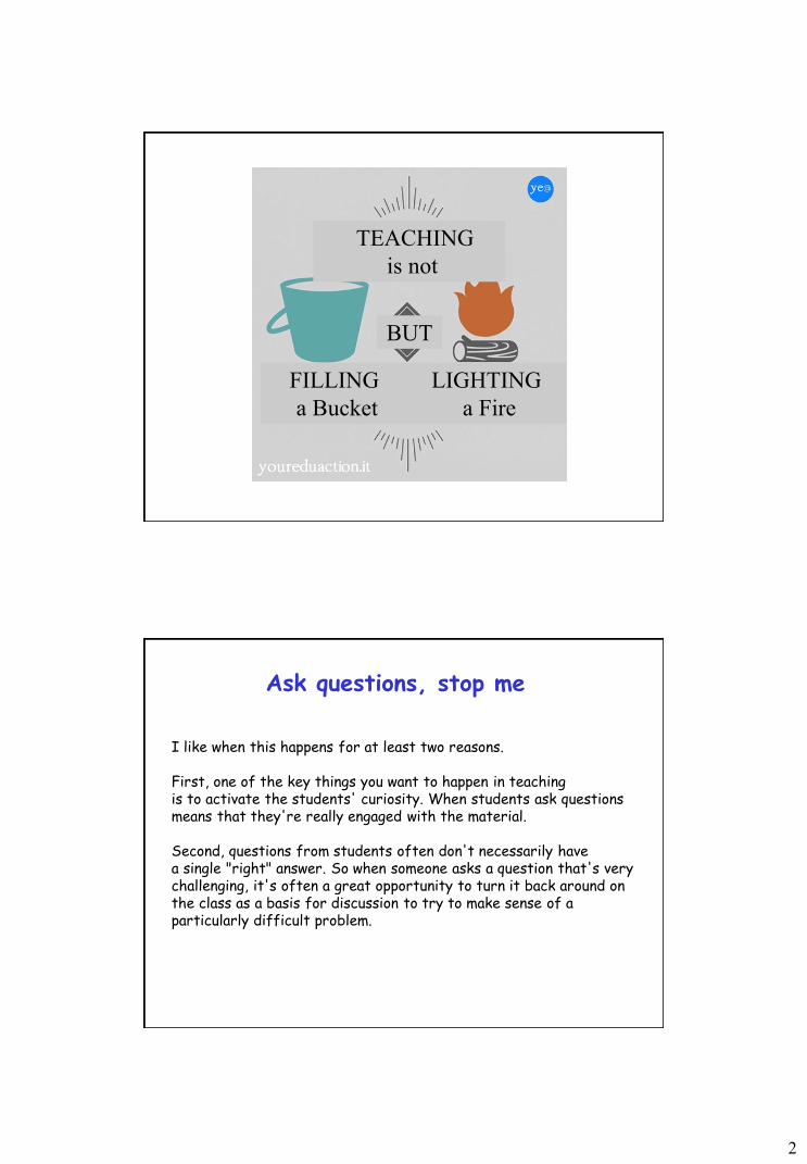
TEACHING
is not
FILLING
a Bucket
LIGHTING
a Fire
BUT
Ask questions, stop me
I like when this happens for at least two reasons.
First, one of the key things you want to happen in teaching is to activate the students' curiosity. When students ask questions means that they're really engaged with the material.
Second, questions from students often don't necessarily have a single "right" answer. So when someone asks a question that's verychallenging, it's often a great opportunity to turn it back around on the class as a basis for discussion to try to make sense of a particularly difficult problem.
3
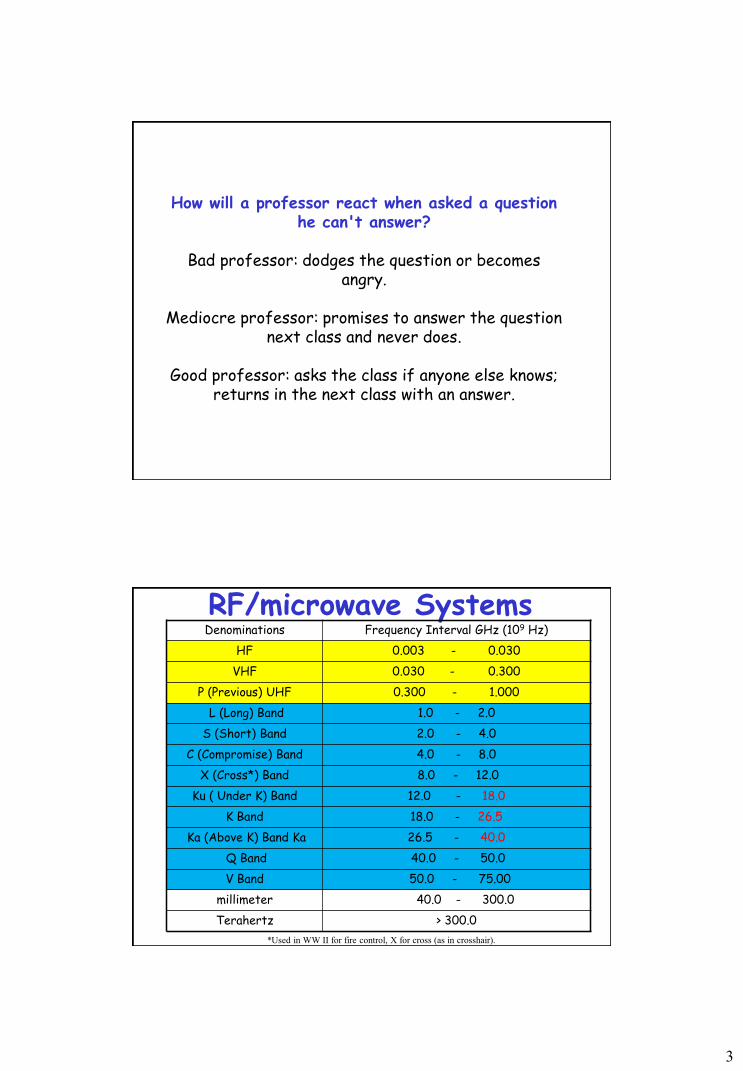
How will a professor react when asked a question he can't answer?
Bad professor: dodges the question or becomes angry.
Mediocre professor: promises to answer the question next class and never does.
Good professor: asks the class if anyone else knows; returns in the next class with an answer.
RF/microwave SystemsDenominations Frequency Interval GHz (109 Hz)
HF 0.003 - 0.030
VHF 0.030 - 0.300
P (Previous) UHF 0.300 - 1.000
L (Long) Band 1.0 - 2.0
S (Short) Band 2.0 - 4.0
C (Compromise) Band 4.0 - 8.0
X (Cross*) Band 8.0 - 12.0
Ku ( Under K) Band 12.0 - 18.0
K Band 18.0 - 26.5
Ka (Above K) Band Ka 26.5 - 40.0
Q Band 40.0 - 50.0
V Band 50.0 - 75.00
millimeter 40.0 - 300.0
Terahertz > 300.0
*Used in WW II for fire control, X for cross (as in crosshair).

4
Discrete Component CircuitsPDIP (Plastic Dual Inline Package)
SMD (Surface-Mounted Device)
Digital TV Transmitter
In Europe Digital Video Broadcast - Terrestrial (DVB-T)
Frequency division multiplexing with orthogonal codes (COFDM)
with 16-QAM or 64-QAM. DVB-S (satellite)
United States

5
DVB-S Receiver
(DVB-S) Uplink 14-14.5 GHz Downlink 10.95 – 12.75 GHz (500 MHz)
RHCP (Right-Hand Circular Polarization) and LHCP polarizations
Terrestrial Receiver-Transmitting(TX/RX) System
(analog signal 2 -13 GHz)
Base-Band signal
Frequency Modulator
Amplifier mixer
Local Oscilaltor
Power Amplifier
Transmitter Antenna
Base-Band Signal
Frequency Demodulator
mixer
Local Oscilaltor Intermediate Frequency Amplifier
Receiving Antenna
Local Oscillator

6
Satellite Transponder(digital signals)
QPSK Demodulator
mixer
Local Oscillator
Intermediate Frequency Amplifier
Receiver Antenna Low-Noise
Amplifier
Rigenerator
Local Oscilaltor
Power Amplifier
Transmitting Antenna
QPSK Modulator
fIN
fOL1 fIN
fOL
Directional Coupler 3 dB Hybrid
Transmitting and Receiving Antenna Microwave
Source Continous Wave
(DRO)
mixer
Doppler Frequency
Body
v(t) = V0 sen(0t) v(t) = V1 sen(1t)
Filter
vIF(t)
Vout(t)
Doppler Radar

7
𝑅 =𝑐02· 𝑇 ·
𝑓𝐵𝐵
FMCW Radar
Course Outline
• INTRODUCTION: Examples of telecommunication and radar systems, example of a project.
• RF OSCILLATORS: resonant circuits, factors of merit and loss, examples of RLC networks, frequencystability coefficient, quartz as a circuit element, phase noise; Colpitts and quartz oscillators. Negative resistance oscillators: steady state and triggeringconditions, dielectric resonator oscillators, ceramicresonator oscillators.
8
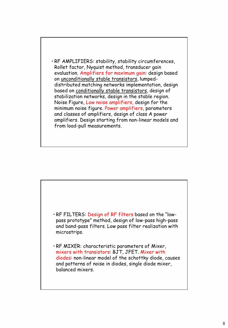
• RF AMPLIFIERS: stability, stability circumferences, Rollet factor, Nyquist method, transducer gain evaluation. Amplifiers for maximum gain: design based on unconditionally stable transistors, lumped-distributed matching networks implementation, design based on conditionally stable transistors, design of stabilization networks, design in the stable region. Noise Figure, Low noise amplifiers, design for the minimum noise figure. Power amplifiers, parameters and classes of amplifiers, design of class A power amplifiers. Design starting from non-linear models and from load-pull measurements.
• RF FILTERS: Design of RF filters based on the “low-pass prototype” method, design of low-pass high-pass and band-pass filters. Low pass filter realization with microstrips.
• RF MIXER: characteristic parameters of Mixer, mixers with transistors: BJT, JFET. Mixer with diodes: non-linear model of the schottky diode, causes and patterns of noise in diodes, single diode mixer, balanced mixers.
9
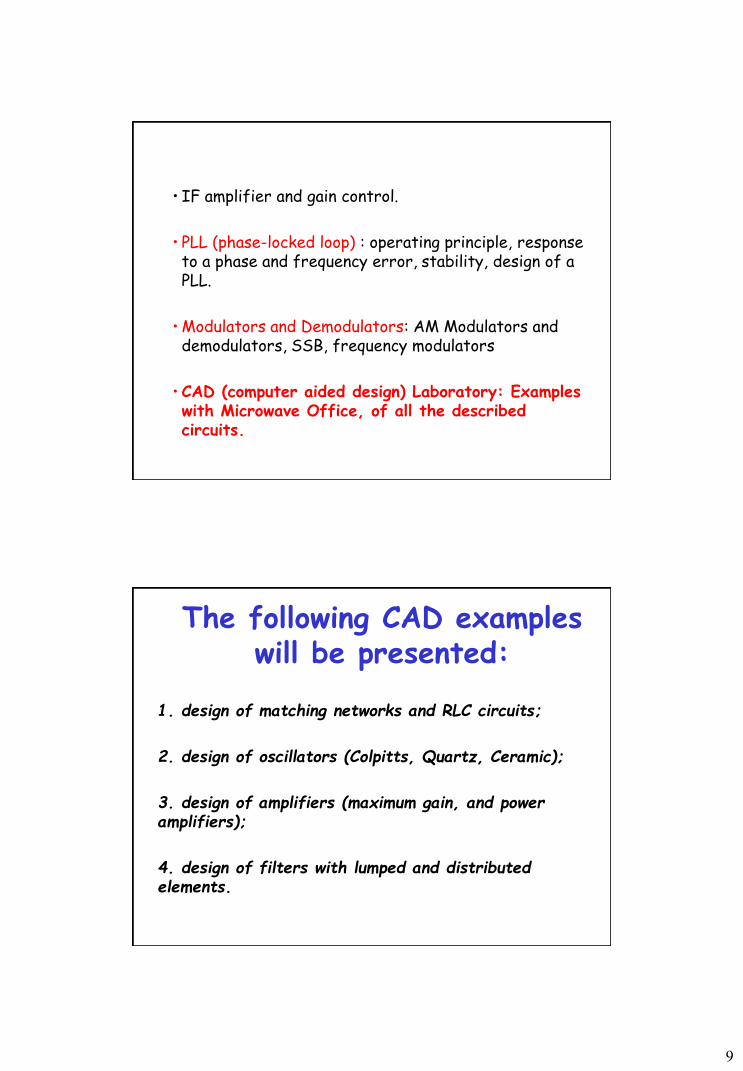
• IF amplifier and gain control.
• PLL (phase-locked loop) : operating principle, response to a phase and frequency error, stability, design of a PLL.
• Modulators and Demodulators: AM Modulators and demodulators, SSB, frequency modulators
• CAD (computer aided design) Laboratory: Examples with Microwave Office, of all the described circuits.
The following CAD examples will be presented:
1. design of matching networks and RLC circuits;
2. design of oscillators (Colpitts, Quartz, Ceramic);
3. design of amplifiers (maximum gain, and power amplifiers);
4. design of filters with lumped and distributed elements.

10
RF ELECTRONIC SYSTEMSHF VHF-UHF MICROWAVES
OSCILLATOR COLPITTS
QUARTZ
COLPITTS
CRO
CRO
DRO
AMPLIFIERS
High Gain Elettronics II Elettronics II REACTIVE
MATCHING
Low Noise Elettronics II Elettronics II REACTIVE
MATCHING
High Power HF
TRASFORMER
VHF UHF
TRASFORMERREACTIVE
MATCHING
MIXER Schottky Diodes
Diplexer
TRANSISTORS
Schottky Diodes
Diplexer
TRANSISTORS
SCHOTTKY DIODES
180° Hybrid
TRANSISTORS
FILTERS LUMPED LUMPED (SMD) MICROSTRIP
MODULATOR, DEMODULATOR
CAD EXERCICES (MICROWAVE OFFICE) ALL THE DESCRIBED CIRCUITS
Course MaterialTextbook:
• Lecture notes available on the web site:
http://mwl.diet.uniroma1.it/people/pisa/RFELSYS.html
Recommended textbooks:
• 1. Kikkert_RF_Electronics_Course
• 2. David M. Pozar, Microwave Engineering, Fourth Edition
• 3. H.L. Krauss et al., Solid State Radio Engineering
• 4. Guillermo Gonzalez, Microwave Transistor Amplifiers
Web sites:
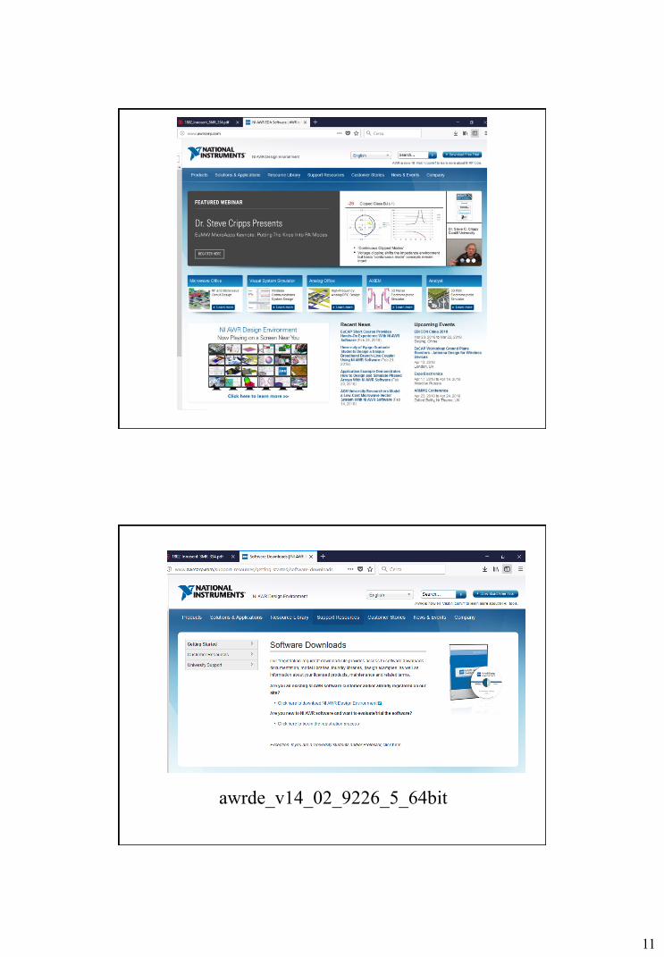
• 1. https://www.rf-microwave.com/en/home/ (italian supplier of RF components)
• 2. http://www.awrcorp.com/products/microwave-office
11
awrde_v14_02_9226_5_64bit

12

13
Grading
Your course grade will be determined as follows:
35% : Oral exam on one topic covered by Prof. Tommasino lectures
35% : Oral exam on one topic covered by Prof. Pisa lectures
30% : MWO project work
Design of RF Circuits1) Design Specifications
2) Dimensioning (Analytical, Smith's Chart, etc.)
3) Layout (CAD)
4) Optimization (CAD)
5) Prototype Realization (Milling Machine, ChemicalEtching)
6) Prototype Measurement

14
Filter design Specifications
• Low Pass Filter
• maximally flat
• Cut-off Frequency, fC = 5.5 GHz
• Cut-off Attenuation, Ac= 3dB
• Out of band Attenuation = 10 dB at 7 GHz
Dimensioning (Ideal)low pass prototype method
Filter Elements N = 5g1=0.618, g2=1.618, g3=2, g4=1.618, g5=0.618
CAP
C=
ID=
0.358 pF
C1 CAP
C=
ID=
1.157 pF
C2
CAP
C=
ID=
0.358 pF
C3
IND
L=
ID=
2.341 nH
L1 IND
L=
ID=
2.341 nH
L2 PORT
Z=
P=
50 Ohm
1
PORT
Z=
P=
50 Ohm
2

15
Dimensioning Results
4 5 6 7 7.5
Frequency (GHz)
1 Risposta in Ampiezza
-30
-20
-10
0
5.5 GHz -3.02
5.5 GHz -2.93
DB(|S[2,1]|)
1 Binomiale
DB(|S[2,1]|)
2 Chebychev
Physical Dimensioning
MSUB
Name=
ErNom=
Tand=
Rho=
T=
H=
Er=
RO1
3.38
0.0027
0.7
0.035 mm
0.508 mm
3.38
MLIN
L=
W=
ID=
0.910 mm
w15 mm
TL1 MLIN
L=
W=
ID=
5.872 mm
w75 mm
TL2 MLIN
L=
W=
ID=
2.947 mm
w15 mm
TL3 MLIN
L=
W=
ID=
5.872 mm
w75 mm
TL4 MLIN
L=
W=
ID=
0.910 mm
w15 mm
TL5 MLIN
L=
W=
ID=
20 mm
w50 mm
TL6 MLIN
L=
W=
ID=
20 mm
w50 mm
TL7 MSTEP
W2=
W1=
ID=
w15 mm
w50 mm
TL8 MSTEP
W2=
W1=
ID=
w75 mm
w15 mm
TL9 MSTEP
W2=
W1=
ID=
w15 mm
w75 mm
TL10 MSTEP
W2=
W1=
ID=
w75 mm
w15 mm
TL11 MSTEP
W2=
W1=
ID=
w15 mm
w75 mm
TL12
MSTEP
W2=
W1=
ID=
w50 mm
w15 mm
TL13 PORT
Z=
P=
50 Ohm
1
PORT
Z=
P=
50 Ohm
2
w50=1.161
w15=5.844
w75=0.544MLIN
L=
W=
ID=
0.910 mm
w15 mm
TL1 MLIN
L=
W=
ID=
5.872 mm
w75 mm
TL2 MSTEP
W2=
W1=
ID=
w75 mm
w15 mm
TL9 w15=5.844
w75=0.544
16
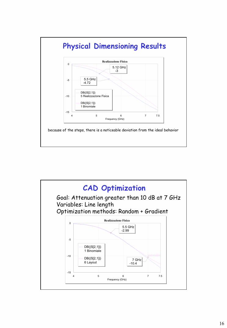
Physical Dimensioning Results
4 5 6 7 7.5
Frequency (GHz)
Realizzazione Fisica
-15
-10
-5
0
5.12 GHz -3
5.5 GHz -4.72
DB(|S[2,1]|)
5 Realizzazione Fisica
DB(|S[2,1]|)
1 Binomiale
because of the steps, there is a noticeable deviation from the ideal behavior
CAD Optimization
4 5 6 7 7.5
Frequency (GHz)
Realizzazione Fisica
-15
-10
-5
0
7 GHz -10.4
5.5 GHz -2.99
DB(|S[2,1]|)
1 Binomiale
DB(|S[2,1]|)
6 Layout
Goal: Attenuation greater than 10 dB at 7 GHzVariables: Line lengthOptimization methods: Random + Gradient
17
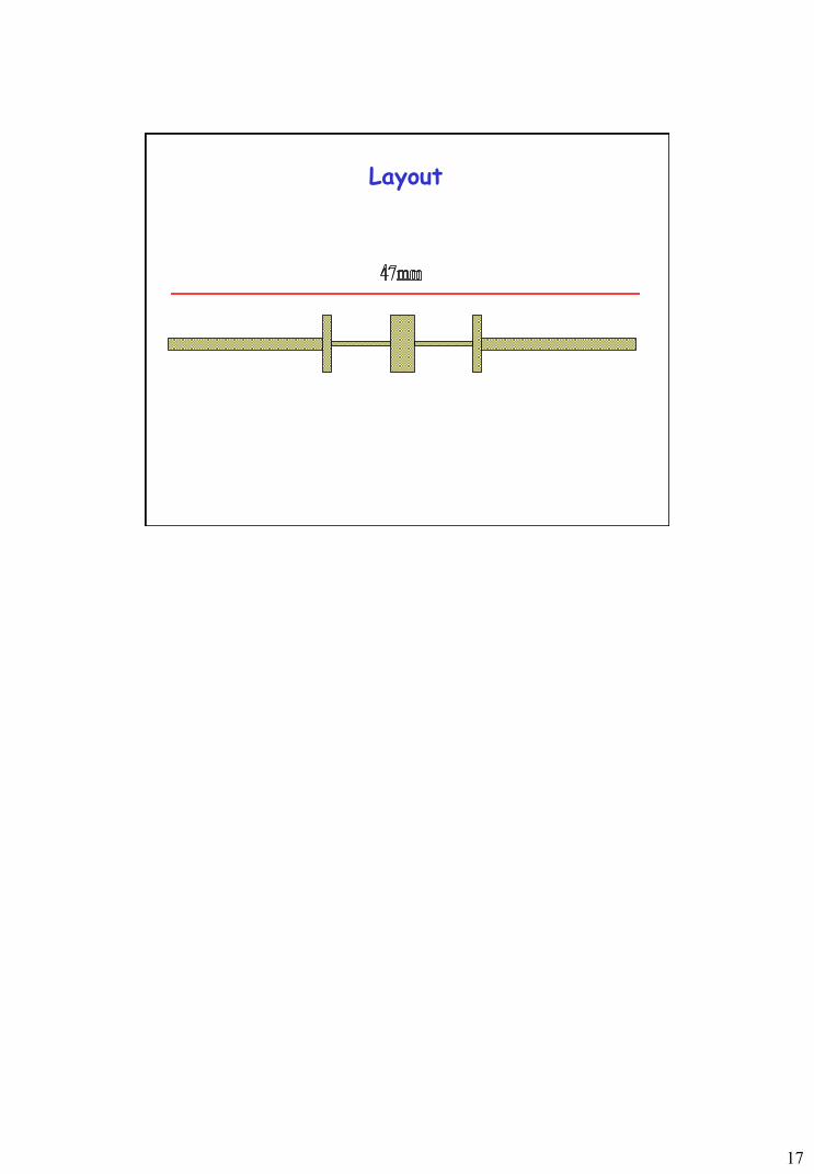
Layout