Radiation Effects in Microelectronics EE-698a Course Seminar by Aashish Agrawal.
38
Radiation Effects in Microelectronics EE-698a Course Seminar by Aashish Agrawal
-
date post
21-Dec-2015 -
Category
Documents
-
view
220 -
download
0
Transcript of Radiation Effects in Microelectronics EE-698a Course Seminar by Aashish Agrawal.

Radiation Effects in Microelectronics
EE-698a Course Seminar by
Aashish Agrawal
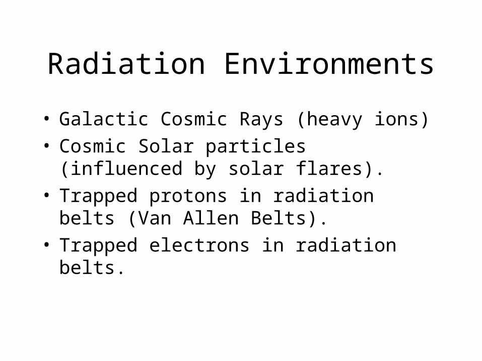
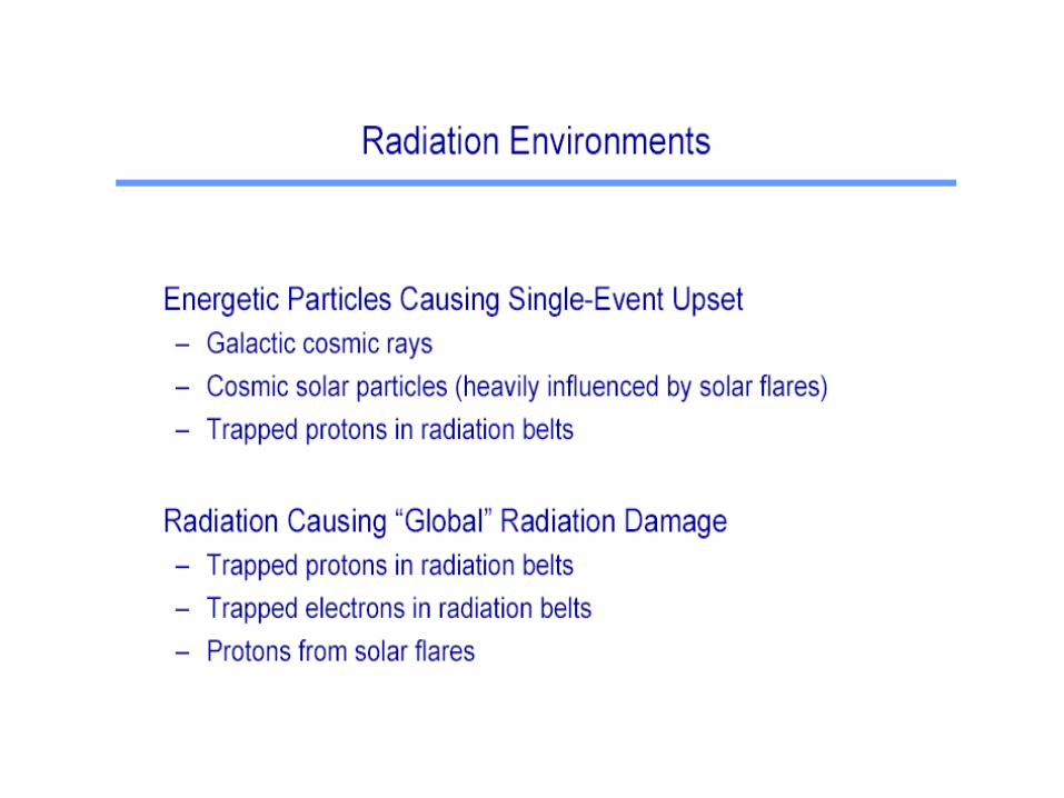
Radiation Environments
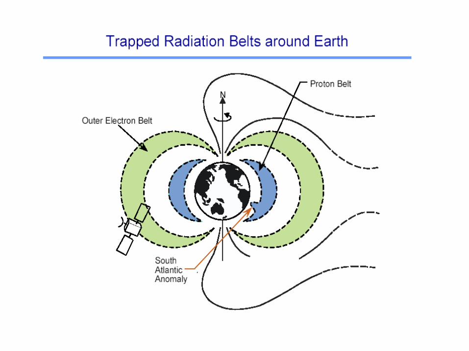
• Galactic Cosmic Rays (heavy ions)• Cosmic Solar particles (influenced by solar flares).• Trapped protons in radiation belts (Van Allen
Belts).• Trapped electrons in radiation belts.


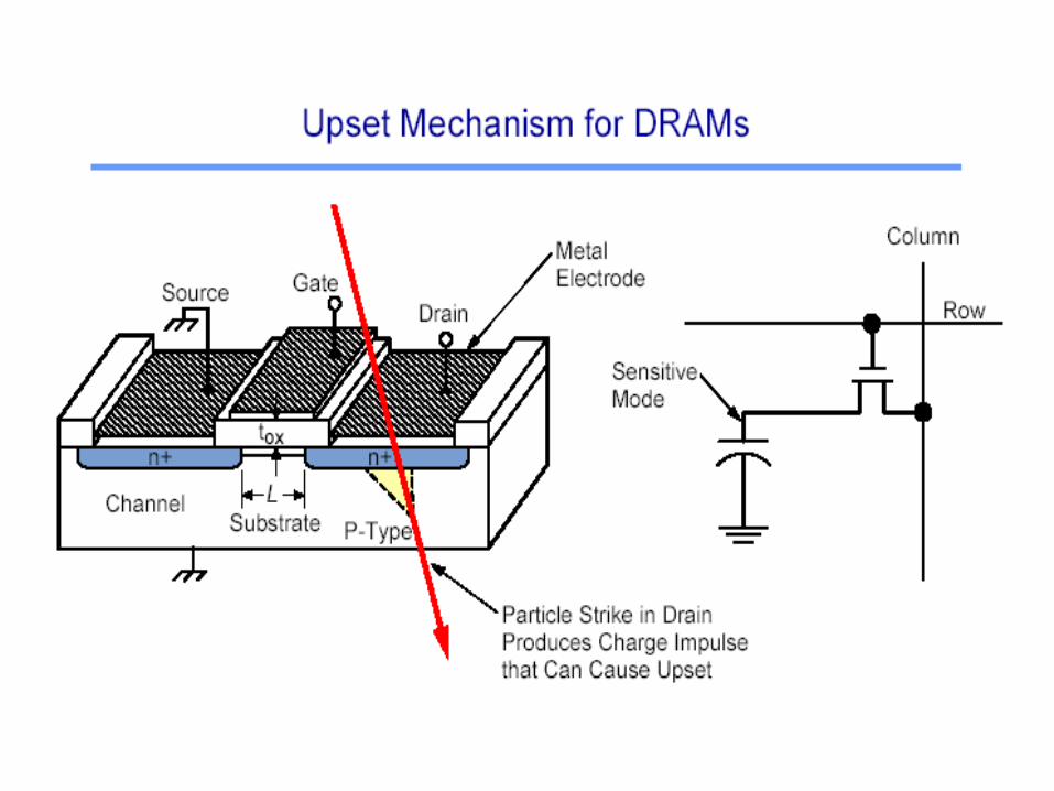
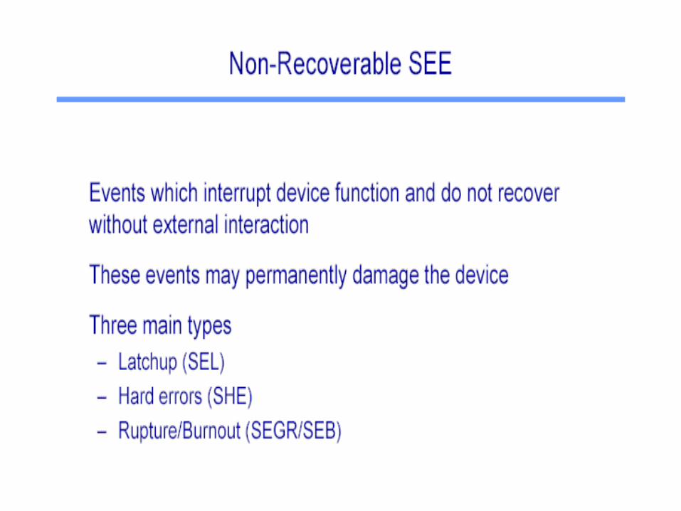
Single Event Upset (SEU)
• Single event upset (SEU) is defined by NASA as "radiation-induced errors in microelectronic circuits caused when charged particles (usually from the radiation belts or from cosmic rays) lose energy by ionizing the medium through which they pass, leaving behind a wake of electron-hole pairs."
• Is a soft SEE.


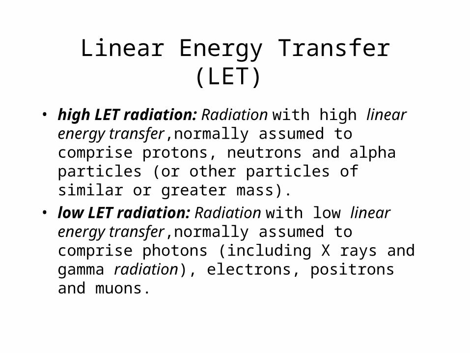
Linear Energy Transfer (LET)
• high LET radiation: Radiation with high linear energy transfer,normally assumed to comprise protons, neutrons and alpha particles (or other particles of similar or greater mass).
• low LET radiation: Radiation with low linear energy transfer,normally assumed to comprise photons (including X rays and gamma radiation), electrons, positrons and muons.
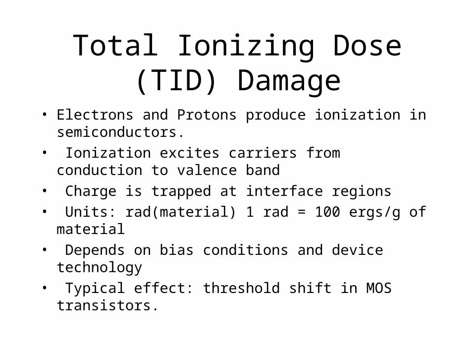
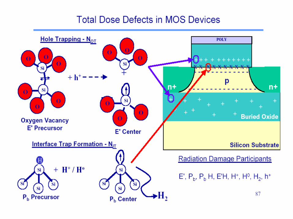
Total Ionizing Dose (TID) Damage
• Electrons and Protons produce ionization in semiconductors.
• Ionization excites carriers from conduction to valence band
• Charge is trapped at interface regions
• Units: rad(material) 1 rad = 100 ergs/g of material
• Depends on bias conditions and device technology
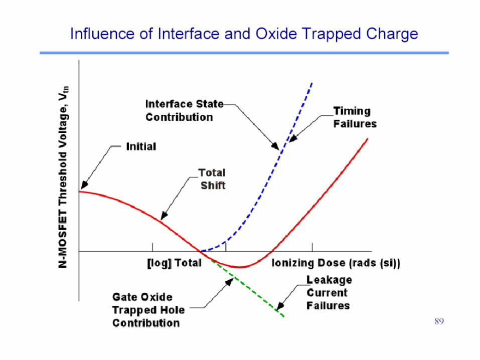
• Typical effect: threshold shift in MOS transistors.
Unit of Total Ionizing Dose (RAD)
• Total ionizing dose in electronics is similar to a sunburn to humans. Total dose is the cumulative ionizing radiation that an electronic device receives over a specified period of time. Like a sunburn to humans, the damage is dependant on the amount of radiation and how long it took to accumulate the total dose. Its Unit is RAD (Radiation Absorbed Dose).


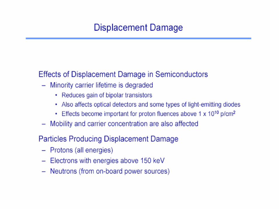
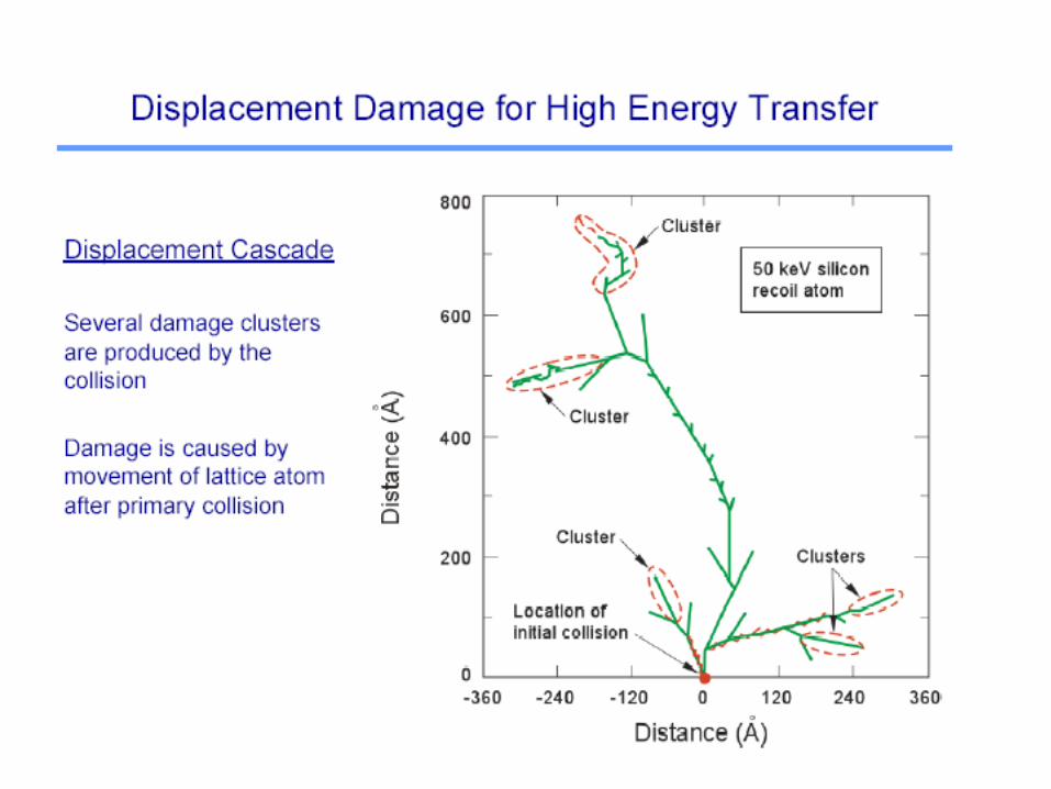
Displacement Damage
• “Collision” between incoming particle and lattice atom.
• Lattice atom is moved out of normal position.
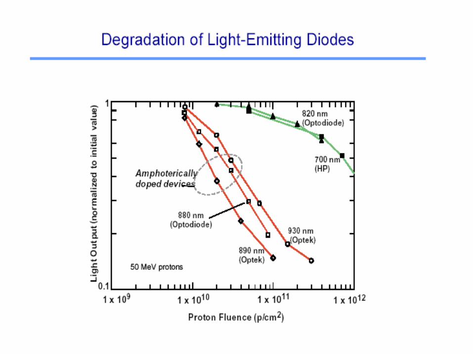
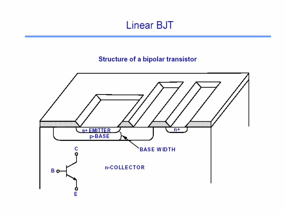
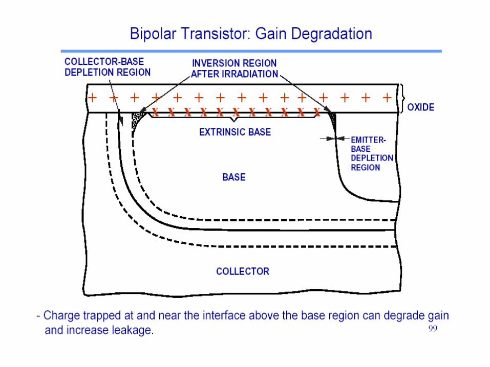
• Degrades minority carrier lifetime.• Typical effect: degradation of gain and
leakage current in bipolar transistors.

Displacement Damage
• N-Type Si: V-P, V-O, V-V are stable defects.
• P-Type Si: V-O, V-V are stable defects.
• Electrical activity of an energy level:– NT Trap Concentration.
– ET Energy level.
– Capture cross section for electrons and holes.
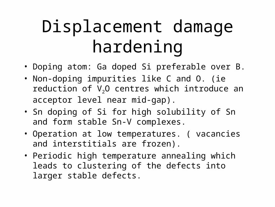
Displacement damage hardening
• Doping atom: Ga doped Si preferable over B.
• Non-doping impurities like C and O. (ie reduction of V2O centres which introduce an acceptor level near mid-gap).
• Sn doping of Si for high solubility of Sn and form stable Sn-V complexes.
• Operation at low temperatures. ( vacancies and interstitials are frozen).
• Periodic high temperature annealing which leads to clustering of the defects into larger stable defects.


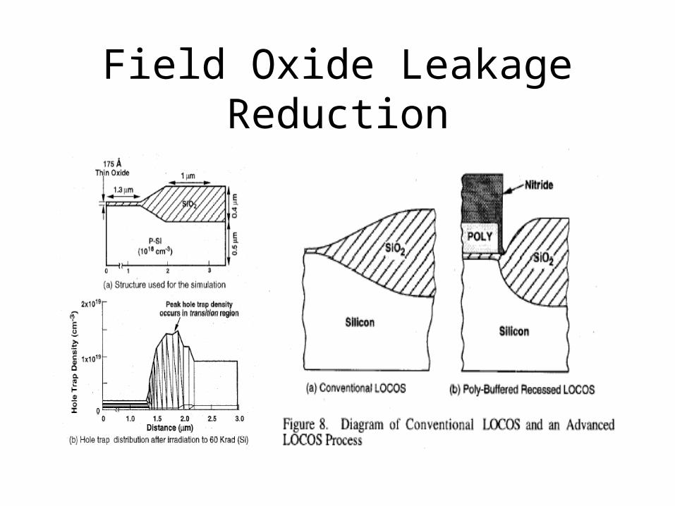
Field Oxide Leakage Reduction


Conclusions
– Single Event Effects (SEE), LET.– Total Ionizing Dose (TID), RAD.
– Displacement Damage. ET, NT.
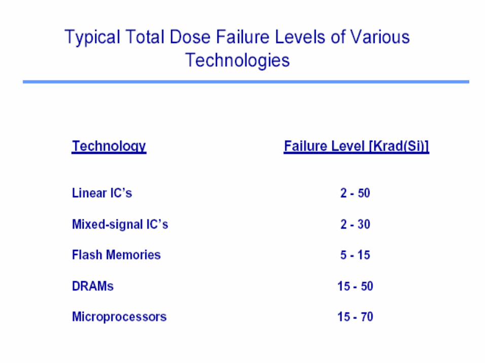
– TID is the primary damage mechanism in MOS and Bipolar devices due to formation of Oxide and Interface Traps.

References
• Claeys C. and Simoen E., Radiation effects in Advanced Semiconductor Materials and Devices (Springer, 2002).
• A.H. Johnston, “Radiation effects in advanced microelectronics technologies”, in IEEE Trans. Nuc. Sci., 45(3) 1998.
• http://parts.jpl.nasa.gov/docs/Radcrs_Final.pdf
• http://www.maxwell.com/microelectronics/products/radtest/intro.html#SEE
• H.P. Hjalmarson, R.L. Pease,”Mechanisms for Radiation Dose-Rate Sensitivity of Bipolar Transistors”. http://www.cs.sandia.gov/departments/9235/papers_pdf/2003_pdf/hman187_eldrs_nsrec_portable03sep17.pdf