search.jsp?R=20110023386 2018-05 … · solder joint type because the ... Tested the theory that...
32
Workmanship Risks: Reworking Printed Circuit Board (PCB) Solder Joints Understanding and managing risks associated with underfilled through-hole solder joints Jeannette Plante Beth Paquette October 18, 2011 11/2/2011 https://ntrs.nasa.gov/search.jsp?R=20110023386 2018-07-03T03:32:45+00:00Z
Transcript of search.jsp?R=20110023386 2018-05 … · solder joint type because the ... Tested the theory that...

Workmanship Risks: Reworking Printed Circuit Board (PCB)
Solder Joints Understanding and managing risks associated
with underfilled through-hole solder joints
Jeannette Plante Beth Paquette
October 18, 2011
11/2/2011
https://ntrs.nasa.gov/search.jsp?R=20110023386 2018-07-03T03:32:45+00:00Z

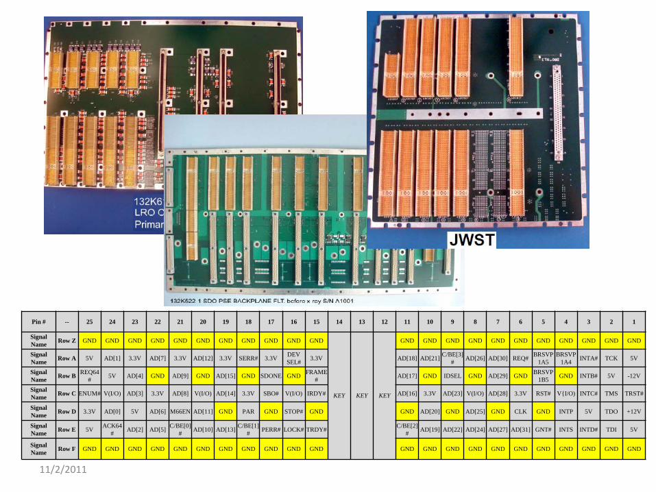
cPCI Solder Joints Routinely Found Underfilled – cPCI style connector becoming standard for NASA backplanes – Hypertronics brand is required to provide non-fretting contacts
and solder tails. Commercial version is a reliability concern: uses tuning fork pin/socket contacts and press-fit board-side contacts.
– Backplane boards are becoming thicker and have increasingly higher percentages of copper (12 layers and counting)
– Soldering is performed by wave soldering machine or by hand. – The typical model used has 100+ pins. Stand-off is 0.50 mm.
11/2/2011 Courtesy: Hypertronics Corporation
11/2/2011
Pin # -- 25 24 23 22 21 20 19 18 17 16 15 14 13 12 11 10 9 8 7 6 5 4 3 2 1
Signal Name Row Z GND GND GND GND GND GND GND GND GND GND GND
KEY KEY KEY
GND GND GND GND GND GND GND GND GND GND GND
Signal Name Row A 5V AD[1] 3.3V AD[7] 3.3V AD[12] 3.3V SERR# 3.3V DEV
SEL# 3.3V AD[18] AD[21] C/BE[3]# AD[26] AD[30] REQ# BRSVP
1A5 BRSVP
1A4 INTA# TCK 5V
Signal Name Row B REQ64
# 5V AD[4] GND AD[9] GND AD[15] GND SDONE GND FRAME# AD[17] GND IDSEL GND AD[29] GND BRSVP
1B5 GND INTB# 5V -12V
Signal Name Row C ENUM# V(I/O) AD[3] 3.3V AD[8] V(I/O) AD[14] 3.3V SBO# V(I/O) IRDY# AD[16] 3.3V AD[23] V(I/O) AD[28] 3.3V RST# V{I/O) INTC# TMS TRST#
Signal Name Row D 3.3V AD[0] 5V AD[6] M66EN AD[11] GND PAR GND STOP# GND GND AD[20] GND AD[25] GND CLK GND INTP 5V TDO +12V
Signal Name Row E 5V ACK64
# AD[2] AD[5] C/BE[0]# AD[10] AD[13] C/BE[1]
# PERR# LOCK# TRDY# C/BE[2]# AD[19] AD[22] AD[24] AD[27] AD[31] GNT# INTS INTD# TDI 5V
Signal Name Row F GND GND GND GND GND GND GND GND GND GND GND GND GND GND GND GND GND GND GND GND GND GND
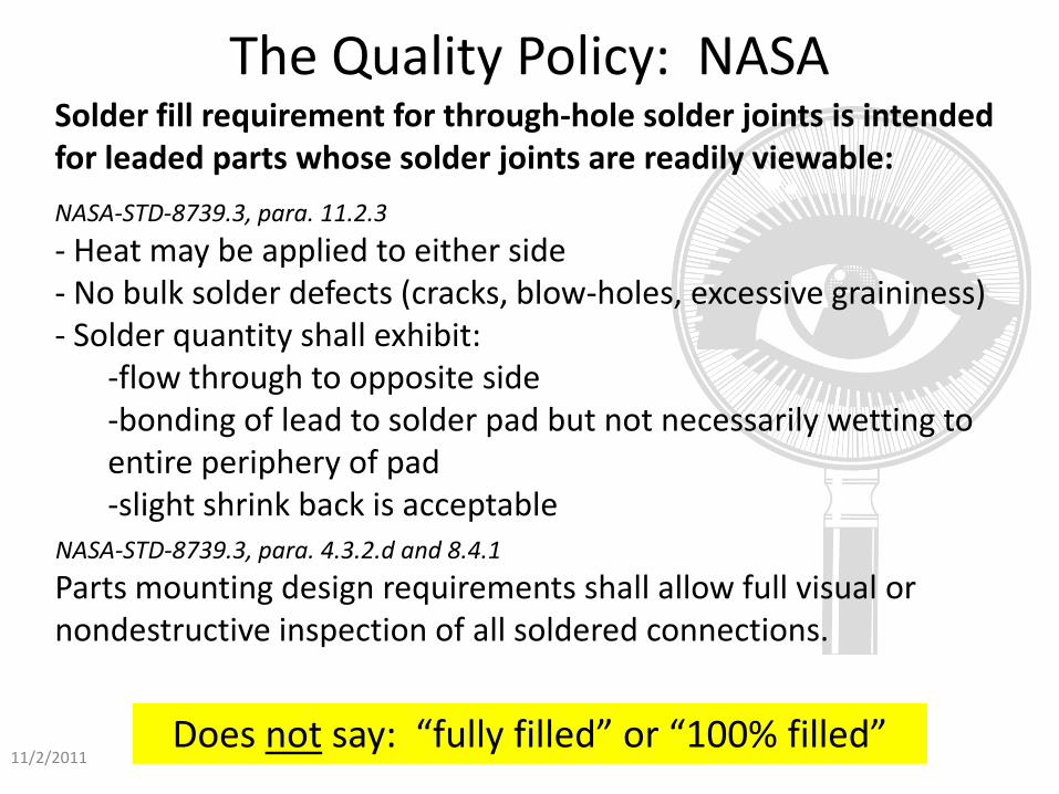
The Quality Policy: NASA
11/2/2011 Does not say: “fully filled” or “100% filled”
Solder fill requirement for through-hole solder joints is intended for leaded parts whose solder joints are readily viewable:
NASA-STD-8739.3, para. 11.2.3 - Heat may be applied to either side - No bulk solder defects (cracks, blow-holes, excessive graininess) - Solder quantity shall exhibit:
-flow through to opposite side -bonding of lead to solder pad but not necessarily wetting to entire periphery of pad -slight shrink back is acceptable
NASA-STD-8739.3, para. 4.3.2.d and 8.4.1 Parts mounting design requirements shall allow full visual or nondestructive inspection of all soldered connections.
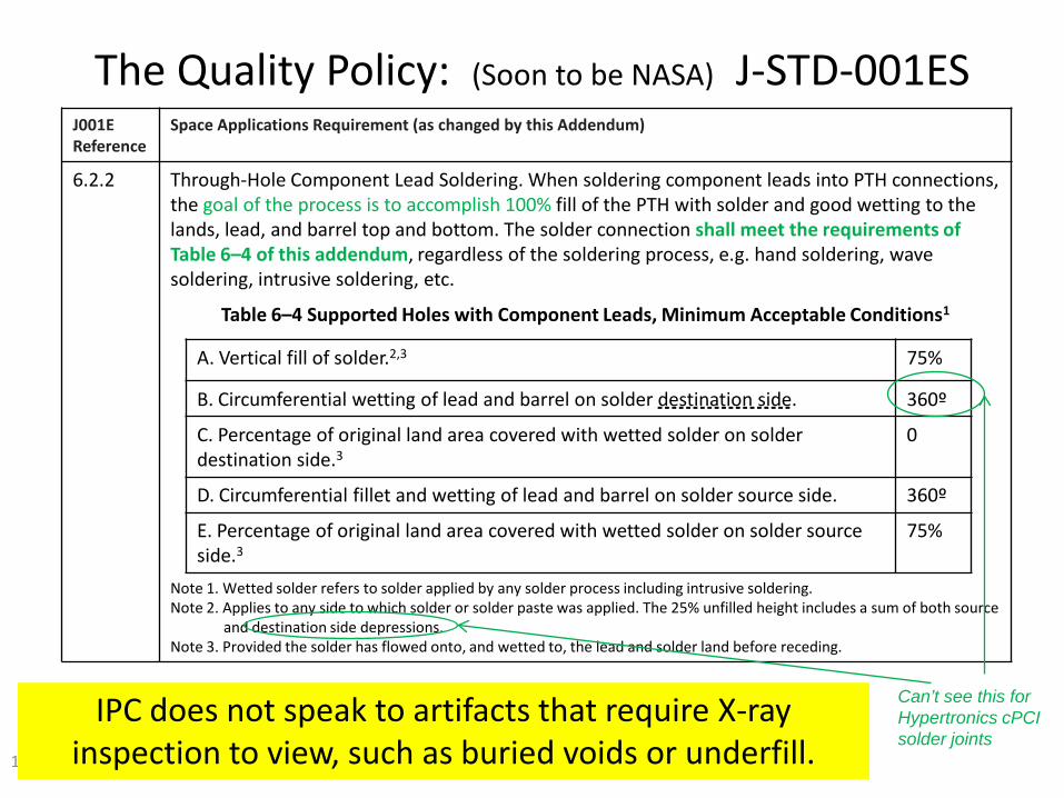
The Quality Policy: (Soon to be NASA) J-STD-001ES
11/2/2011
J001E Reference
Space Applications Requirement (as changed by this Addendum)
6.2.2 Through-Hole Component Lead Soldering. When soldering component leads into PTH connections, the goal of the process is to accomplish 100% fill of the PTH with solder and good wetting to the lands, lead, and barrel top and bottom. The solder connection shall meet the requirements of Table 6–4 of this addendum, regardless of the soldering process, e.g. hand soldering, wave soldering, intrusive soldering, etc.
Table 6–4 Supported Holes with Component Leads, Minimum Acceptable Conditions1
A. Vertical fill of solder.2,3 75%
B. Circumferential wetting of lead and barrel on solder destination side. 360º
C. Percentage of original land area covered with wetted solder on solder destination side.3
0
D. Circumferential fillet and wetting of lead and barrel on solder source side. 360º
E. Percentage of original land area covered with wetted solder on solder source side.3
75%
Note 1. Wetted solder refers to solder applied by any solder process including intrusive soldering. Note 2. Applies to any side to which solder or solder paste was applied. The 25% unfilled height includes a sum of both source
and destination side depressions. Note 3. Provided the solder has flowed onto, and wetted to, the lead and solder land before receding.
Can’t see this for Hypertronics cPCI solder joints
IPC does not speak to artifacts that require X-ray inspection to view, such as buried voids or underfill.

11/2/2011

What are the failure modes that we are trying to prevent? Electrical “open” or unacceptable increase in connection resistance. What causes this change in electrical connectivity? - full or nearly full disconnection with the device lead. - full or nearly full disconnection between solder and barrel wall and solder pad - lack of solder + 360° barrel crack isolates PCB layers from lower/upper layers. - barrel crack or trace crack separates trace from the barrel.
11/2/2011
bulk solder cracks
Source: R.N. Wild
Trace-to-barrel cracks

11/2/2011
Missing or disconnected solder doesn’t always result in electrical failure for this solder joint type because the barrel/solder configuration is highly redundant. The most non-redundant part of the interconnect is between the trace and barrel. Solder and barrel/trace failures often go undetected at room temperature and are detected at high temperature during testing.

11/2/2011
Will an underfilled through-hole joint have a shorter trip to failure than a fully filled joint? How will it tend to fail? If fully filled joints last longer, should we try to fix underfilled joints with rework?
1. Lea, Colin. “Evidence that Visual Inspection Criteria for Soldered Joints are No Indication of Reliability”, Soldering and Surface Mount Technology, 1991, vol. 3, issue 3, pp19-24.
2. Lea, Colin. “The Effect of Blowholes in Soldered PTH Assemblies” 3. Lea, Colin. “The Harmfulness of Re-Working Cosmetically Defective Solder Joints”: 4. Keller, J; Waszczak, J. “The Case for Unfilled PTHs,” Electronics Packaging and Production, 1973,
vol. 13, issue 10, pp144-149 5. Wild, R.N.; “Thermal Characterization of Multilayer Interconnection Boards,” The Institute of
Printed Circuits Conference, Orlando, FL, April 1977. 6. Garrison, Ann; Lee, Mike; Park, Hyun; and Todd, Norma Lee. “How Much is too Much?: The
Effects of Solder Joint Rework on Plated-Through Holes in Multilayer Printed Wiring Boards”, 1994 7. Electronics Manufacturing Productivity Facility. “Tri-Service Evaluation of Field Electronic
Hardware,” June 1990
11/2/2011
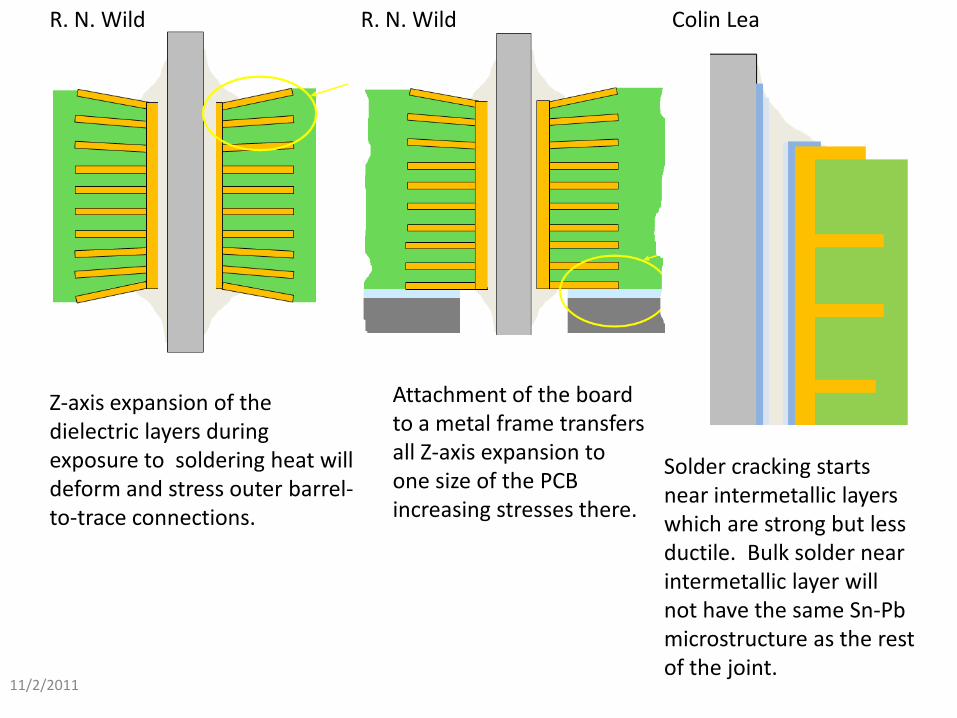
Z-axis expansion of the dielectric layers during exposure to soldering heat will deform and stress outer barrel-to-trace connections.
Attachment of the board to a metal frame transfers all Z-axis expansion to one size of the PCB increasing stresses there.
Solder cracking starts near intermetallic layers which are strong but less ductile. Bulk solder near intermetallic layer will not have the same Sn-Pb microstructure as the rest of the joint.
R. N. Wild R. N. Wild Colin Lea
11/2/2011
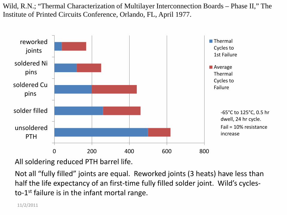
0 200 400 600 800
unsoldered PTH
solder filled
soldered Cu pins
soldered Ni pins
reworked joints
Thermal Cycles to 1st Failure
Average Thermal Cycles to Failure
-65°C to 125°C, 0.5 hr dwell, 24 hr cycle. Fail = 10% resistance increase
All soldering reduced PTH barrel life. Not all “fully filled” joints are equal. Reworked joints (3 heats) have less than half the life expectancy of an first-time fully filled solder joint. Wild’s cycles-to-1st failure is in the infant mortal range.
Wild, R.N.; “Thermal Characterization of Multilayer Interconnection Boards – Phase II,” The Institute of Printed Circuits Conference, Orlando, FL, April 1977.
11/2/2011
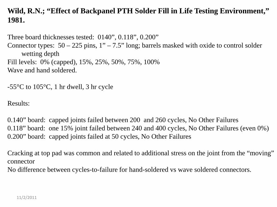
Wild, R.N.; “Effect of Backpanel PTH Solder Fill in Life Testing Environment,” 1981. Three board thicknesses tested: 0140”, 0.118”, 0.200” Connector types: 50 – 225 pins, 1” – 7.5” long; barrels masked with oxide to control solder
wetting depth Fill levels: 0% (capped), 15%, 25%, 50%, 75%, 100% Wave and hand soldered. -55°C to 105°C, 1 hr dwell, 3 hr cycle Results: 0.140” board: capped joints failed between 200 and 260 cycles, No Other Failures 0.118” board: one 15% joint failed between 240 and 400 cycles, No Other Failures (even 0%) 0.200” board: capped joints failed at 50 cycles, No Other Failures Cracking at top pad was common and related to additional stress on the joint from the “moving” connector No difference between cycles-to-failure for hand-soldered vs wave soldered connectors.

11/2/2011
Keller, J; Waszczak, J. “The Case for Unfilled PTHs,” Electronics Packaging and Production, 1973, vol. 13, issue 10, pp144-149 Jeannette paraphrases:
Often you cannot inspect PTH solder fill on the component side: recognizes IPC requirement which cannot be achieved with many connectors.
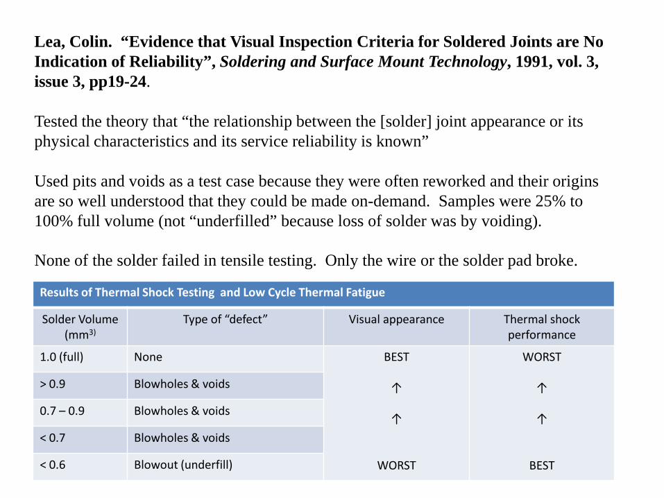
If you have accepted the PCB lot, why not rely on a single end of a through-hole solder joint which is electrically the same node as the second side as well as the internal barrel surface? Lea, Colin. “Evidence that Visual Inspection Criteria for Soldered Joints are No Indication of Reliability”, Soldering and Surface Mount Technology, 1991, vol. 3, issue 3, pp19-24. Tested the theory that “the relationship between the [solder] joint appearance or its physical characteristics and its service reliability is known” Used pits and voids as a test case because they were often reworked and their origins are so well understood that they could be made on-demand. Samples were 25% to 100% full volume (not “underfilled” because loss of solder was by voiding).
11/2/2011
Lea, Colin. “Evidence that Visual Inspection Criteria for Soldered Joints are No Indication of Reliability”, Soldering and Surface Mount Technology, 1991, vol. 3, issue 3, pp19-24. Tested the theory that “the relationship between the [solder] joint appearance or its physical characteristics and its service reliability is known” Used pits and voids as a test case because they were often reworked and their origins are so well understood that they could be made on-demand. Samples were 25% to 100% full volume (not “underfilled” because loss of solder was by voiding). None of the solder failed in tensile testing. Only the wire or the solder pad broke.
Results of Thermal Shock Testing and Low Cycle Thermal Fatigue
Solder Volume (mm3)
Type of “defect” Visual appearance Thermal shock performance
1.0 (full) None BEST
↑
↑
WORST
WORST
↑
↑
BEST
> 0.9 Blowholes & voids
0.7 – 0.9 Blowholes & voids
< 0.7 Blowholes & voids
< 0.6 Blowout (underfill)
11/2/2011
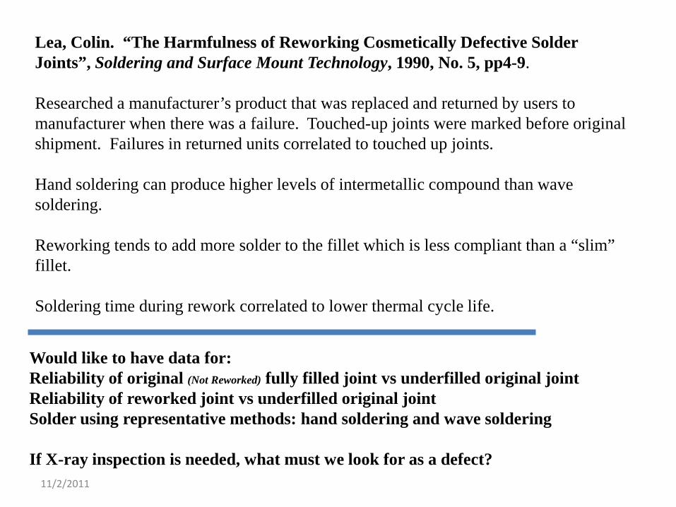
Lea, Colin. “The Harmfulness of Reworking Cosmetically Defective Solder Joints”, Soldering and Surface Mount Technology, 1990, No. 5, pp4-9. Researched a manufacturer’s product that was replaced and returned by users to manufacturer when there was a failure. Touched-up joints were marked before original shipment. Failures in returned units correlated to touched up joints. Hand soldering can produce higher levels of intermetallic compound than wave soldering. Reworking tends to add more solder to the fillet which is less compliant than a “slim” fillet. Soldering time during rework correlated to lower thermal cycle life.
Would like to have data for: Reliability of original (Not Reworked) fully filled joint vs underfilled original joint Reliability of reworked joint vs underfilled original joint Solder using representative methods: hand soldering and wave soldering If X-ray inspection is needed, what must we look for as a defect?
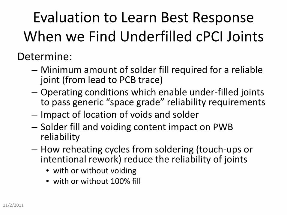
Evaluation to Learn Best Response When we Find Underfilled cPCI Joints
Determine: – Minimum amount of solder fill required for a reliable
joint (from lead to PCB trace) – Operating conditions which enable under-filled joints
to pass generic “space grade” reliability requirements – Impact of location of voids and solder – Solder fill and voiding content impact on PWB
reliability – How reheating cycles from soldering (touch-ups or
intentional rework) reduce the reliability of joints • with or without voiding • with or without 100% fill
11/2/2011
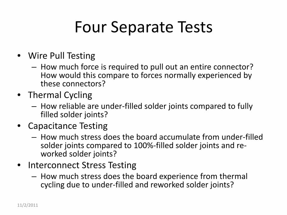
Four Separate Tests • Wire Pull Testing
– How much force is required to pull out an entire connector? How would this compare to forces normally experienced by these connectors?
• Thermal Cycling – How reliable are under-filled solder joints compared to fully
filled solder joints? • Capacitance Testing
– How much stress does the board accumulate from under-filled solder joints compared to 100%-filled solder joints and re-worked solder joints?
• Interconnect Stress Testing – How much stress does the board experience from thermal
cycling due to under-filled and reworked solder joints?
11/2/2011
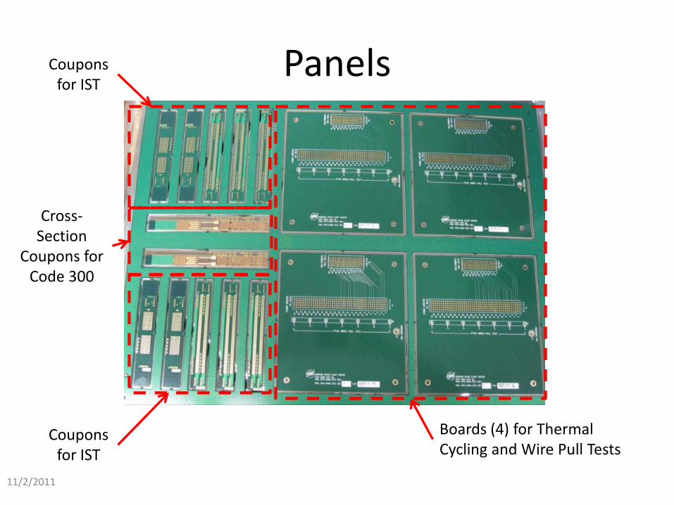
Panels
11/2/2011
Boards (4) for Thermal Cycling and Wire Pull Tests
Coupons for IST
Cross-Section
Coupons for Code 300
Coupons for IST

Assembly • Bake out boards for 24 hours to remove moisture • Reflow boards to simulate surface mount component assembly
(cPCI connectors are installed last) • Developed method of hand soldering for consistent fill amounts
– Small gauge tin-lead solder wire – Larger sized solder tip – 300˚C soldering iron – Vary time of solder application
• 100% fill: 5 seconds • 30-50% fill: 2-3 seconds • Less than 30% fill: 1 second
– Visits to BAE Systems in Manassas, VA to learn sample prep techniques – Practice
• Wave soldering performed at GSFC subcontractor – Preheat boards – Time solder wave
11/2/2011

11/2/2011
0
1
2
3
4
5
6
7
0% 20% 40% 60% 80% 100%
Han
d So
lder
App
licat
ion
Tim
ing
(s)
Percent Fill
Solder Settings versus Solder Fill
Wave Solder
Hand Soldering
Wave Solder Settings
10 Feet Per Minute, 0.35 inches from Wave
12 Feet Per Minute, 0.35 inches from Wave

Fill Calculation
• Record quantity of solder in grams • Examine using X-Ray
– Calculate fill using photos – pixel count
11/2/2011 Fill Amount
Qua
ntity
of P
ins
0
10
20
30
40
>75% 51%-75% 26%-50% <25%
Fill Level Tally
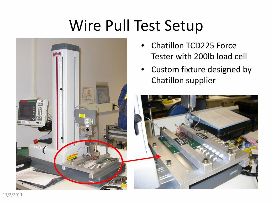
Wire Pull Test Setup • Chatillon TCD225 Force
Tester with 200lb load cell • Custom fixture designed by
Chatillon supplier
11/2/2011

cPCI Wire Pull Testing • Pull on pins soldered to board • Axial stress on wire, shear stress on solder-to-wire
connection • Pull until:
– Pin breaks – Solder connection breaks
• Record force when failure occurs • How does breaking force relate to:
– Shock event? – High-cycle fatigue event? – Mating/De-mating event?
11/2/2011
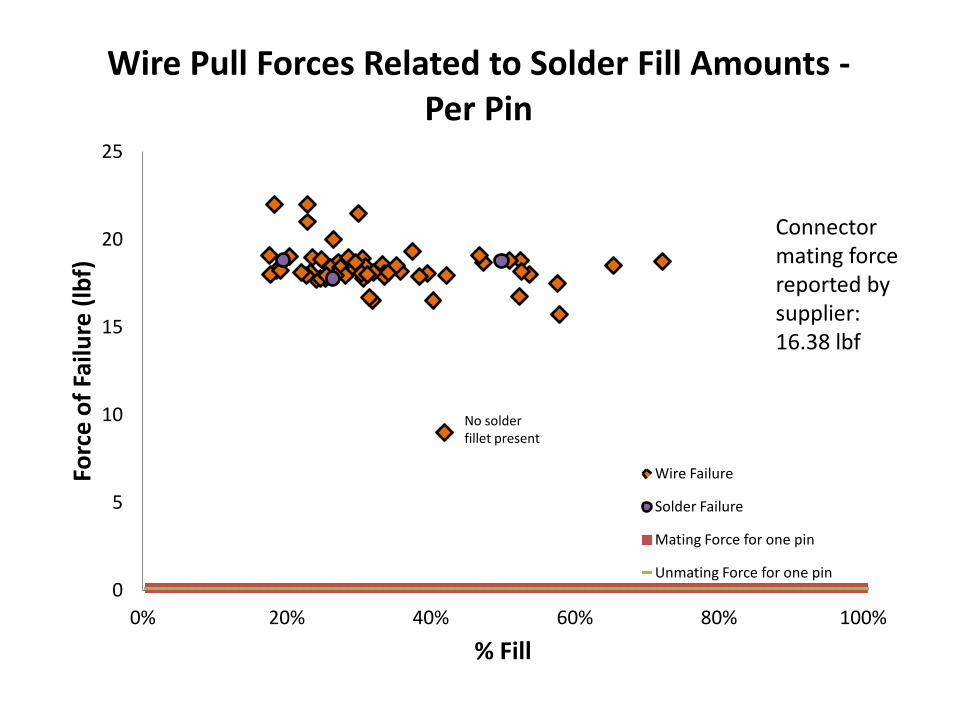
0
5
10
15
20
25
0% 20% 40% 60% 80% 100%
Forc
e of
Fai
lure
(lbf
)
% Fill
Wire Pull Forces Related to Solder Fill Amounts - Per Pin
Wire Failure
Solder Failure
Mating Force for one pin
Unmating Force for one pin
No solder fillet present
Connector mating force reported by supplier: 16.38 lbf

Results to Normalized to Connector
11/2/2011
0
500
1000
1500
2000
2500
3000
3500
0% 20% 40% 60% 80% 100%
Forc
e of
Fai
lure
(lbf
)
% Fill
Wire Failure Solder Failure
No solder fillet
Connector mating force reported by supplier: 16.38lbf De-mating force: 13.2lbf
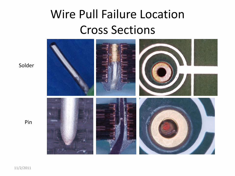
Wire Pull Failure Location Cross Sections
11/2/2011
Solder
Pin

Wire Pull Failure Locations
11/2/2011
Pad
PTH
Note: These failures only seen when wires soldered in from the top of the board. – not relatable to cPCI connector solder joints as the connectors are soldered from the bottom.
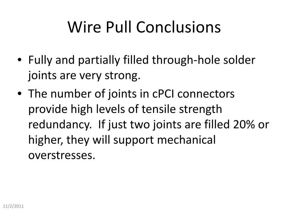
Wire Pull Conclusions
• Fully and partially filled through-hole solder joints are very strong.
• The number of joints in cPCI connectors provide high levels of tensile strength redundancy. If just two joints are filled 20% or higher, they will support mechanical overstresses.
11/2/2011

Test Vehicle #2: Thermal Cycling
11/2/2011
Compressor Oven
Analysis Tech 105 Series Event
Detector
Cycle: -40˚C to +90˚C, 106 minutes
Mated Connector pair
Event Detector Connections for all 110 channels
Supported by Standoffs
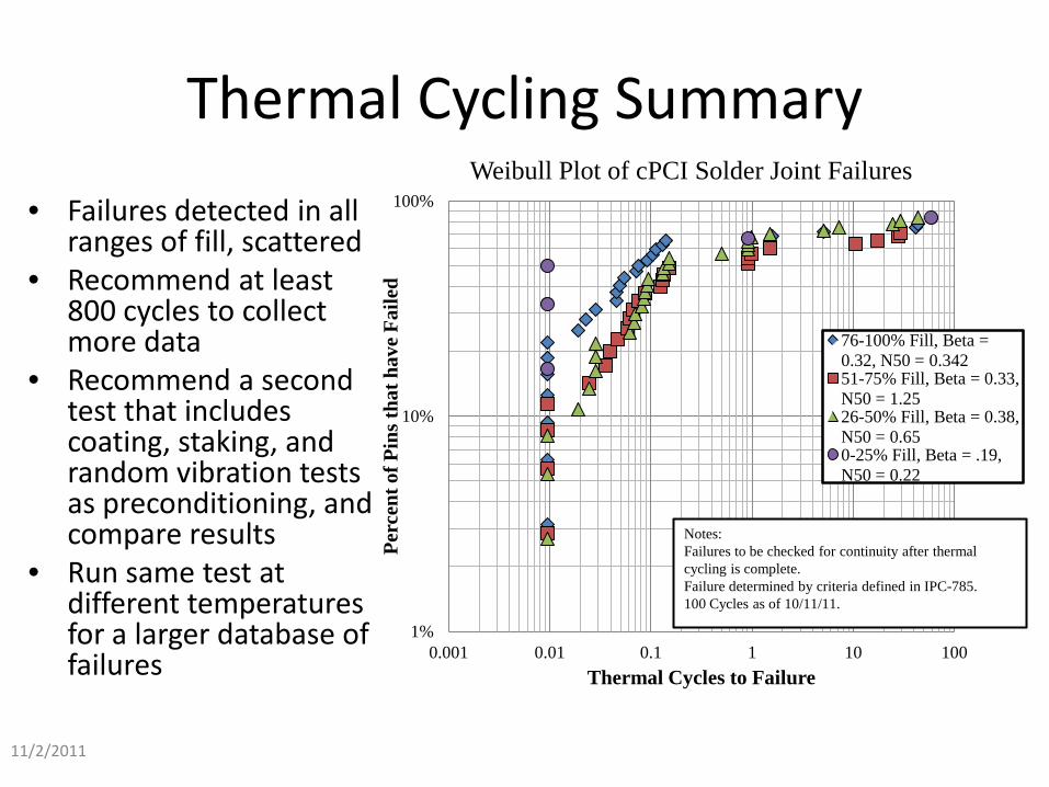
Thermal Cycling Summary
• Failures detected in all ranges of fill, scattered
• Recommend at least 800 cycles to collect more data
• Recommend a second test that includes coating, staking, and random vibration tests as preconditioning, and compare results
• Run same test at different temperatures for a larger database of failures
11/2/2011
1%
10%
100%
0.001 0.01 0.1 1 10 100
Perc
ent o
f Pin
s tha
t hav
e Fa
iled
Thermal Cycles to Failure
76-100% Fill, Beta = 0.32, N50 = 0.342 51-75% Fill, Beta = 0.33, N50 = 1.25 26-50% Fill, Beta = 0.38, N50 = 0.65 0-25% Fill, Beta = .19, N50 = 0.22
Notes: Failures to be checked for continuity after thermal cycling is complete. Failure determined by criteria defined in IPC-785. 100 Cycles as of 10/11/11.
Weibull Plot of cPCI Solder Joint Failures
Future Work
• Finish and resolve thermal cycling testing and results.
• Study Reworked vs Original joint • Round robin evaluation of X-ray inspection
results • Can Interconnect Stress Testing (IST)
demonstrate through-hole joint reliability?
11/2/2011

Acknowledgements Amy Acton Bill Birch Chris Green Chris Greenwell Richard Guild Howard Mills Eleanya Onuma Lester Meggett Corinne Nakashima Larry Pack Lyudmyla Panashchenko Jeannette Plante Marcellus Proctor
Denise Ratliff Chris Reinking Amir Sadeghi Kusum Sahu Nilesh Shah Michael Solly Ken Tran Banks Walker Richard Williams Al Lookingland, Northrop Grumman
11/2/2011