R08DS0123EJ0100 ANALOG OUTPUT TYPE OPTICAL … · The PS8551AL4 is an optically coupled isolation...
20
R08DS0123EJ0100 Rev.1.00 Page 1 of 18 Jun 27, 2014 1. VDD1 2. VIN+ 3. VIN– 4. GND1 5. GND2 6. VOUT– 7. VOUT+ 8. VDD2 PIN CONNECTION (Top View) 1 2 4 3 6 5 8 7 SHIELD + – + – Preliminary Data Sheet PS8551AL4 ANALOG OUTPUT TYPE OPTICAL COUPLED ISOLATION AMPLIFIER DESCRIPTION The PS8551AL4 is an optically coupled isolation amplifier that uses an IC with a high-accuracy sigma-delta A/D converter and a GaAIAs light-emitting diode with high-speed response and high luminance efficiency on the input side, and an IC with a high-accuracy D/A converter on the output side. The PS8551AL4 is designed specifically for high common mode transient immunity (CMTI) and high linearity (non- linearity). The PS8551AL4 is designed for current and voltage sensing. FEATURES • Non-linearity (NL200 = 0.35% MAX.) • High common mode transient immunity (CMTI = 10 kV/μs MIN.) • High isolation voltage (BV = 5 000 Vr.m.s.) • Gain tolerance (G = 7.92 to 8.08 (±1%)) Gain: 8 V/V TYP. • Package: 8-pin DIP lead bending type (Gull-wing) for long creepage distance for surface mount (L4) • Embossed tape product: PS8551AL4-E3: 1 000 pcs/reel • Pb-Free product • Safety standards • UL approved: No. E72422 • CSA approved: No. CA 101391 (CA5A, CAN/CSA-C22.2 60065, 60950) • SEMKO approved (EN60065, EN60950) • DIN EN60747-5-5 (VDE0884-5) approved (Option) APPLICATIONS • AC Servo, inverter • Solar power conditioner • Measurement equipment R08DS0123EJ0100 Rev.1.00 Jun 27, 2014
Transcript of R08DS0123EJ0100 ANALOG OUTPUT TYPE OPTICAL … · The PS8551AL4 is an optically coupled isolation...

R08DS0123EJ0100 Rev.1.00 Page 1 of 18 Jun 27, 2014
1. VDD12. VIN+
3. VIN–
4. GND15. GND26. VOUT–
7. VOUT+
8. VDD2
PIN CONNECTION(Top View)
1 2 43
6 58 7
SHIE
LD
+ –
+ –
Preliminary
Data Sheet PS8551AL4 ANALOG OUTPUT TYPE OPTICAL COUPLED ISOLATION AMPLIFIER
DESCRIPTION The PS8551AL4 is an optically coupled isolation amplifier that uses an IC with a high-accuracy sigma-delta A/D
converter and a GaAIAs light-emitting diode with high-speed response and high luminance efficiency on the input side, and an IC with a high-accuracy D/A converter on the output side.
The PS8551AL4 is designed specifically for high common mode transient immunity (CMTI) and high linearity (non-linearity). The PS8551AL4 is designed for current and voltage sensing.
FEATURES • Non-linearity (NL200 = 0.35% MAX.)• High common mode transient immunity (CMTI = 10 kV/μs MIN.)• High isolation voltage (BV = 5 000 Vr.m.s.)• Gain tolerance (G = 7.92 to 8.08 (±1%))
Gain: 8 V/V TYP.• Package: 8-pin DIP lead bending type (Gull-wing) for long creepage distance for
surface mount (L4)• Embossed tape product: PS8551AL4-E3: 1 000 pcs/reel• Pb-Free product• Safety standards
• UL approved: No. E72422• CSA approved: No. CA 101391 (CA5A, CAN/CSA-C22.2 60065, 60950)• SEMKO approved (EN60065, EN60950)• DIN EN60747-5-5 (VDE0884-5) approved (Option)
APPLICATIONS • AC Servo, inverter• Solar power conditioner• Measurement equipment
R08DS0123EJ0100Rev.1.00
Jun 27, 2014

PS8551AL4 Chapter Title
R08DS0123EJ0100 Rev.1.00 Page 2 of 18 Jun 27, 2014
PACKAGE DIMENSIONS (UNIT: mm)
Lead Bending Type (Gull-wing) For Long Creepage Distance For Surface Mount (L4)
9.25+0.5 –0.25
6.5+0.5–0.1
10.05±0.4
0.62±0.25
0.2±
0.15
3.7±
0.35
3.5±
0.2
1.01+0.4–0.2
2.540.5±0.15
PHOTOCOUPLER CONSTRUCTION
Parameter Unit (MIN.)
Air Distance 8 mm
Outer Creepage Distance 8 mm
Isolation Distance 0.4 mm

PS8551AL4 Chapter Title
R08DS0123EJ0100 Rev.1.00 Page 3 of 18 Jun 27, 2014
MARKING EXAMPLE
R8551ANT131
No. 1 pinMark
1 31
Year Assembled(Last 1 Digit)
TN
Rank Code
In-house Code(T: Pb-Free)
Week Assembled
Assembly Lot
Type Number
Company Initial
ORDERING INFORMATION
Part Number Order Number Solder Plating
Specification
Packing Style Safety Standard
Approval
Application Part
Number*1
PS8551AL4 PS8551AL4-AX Pb-Free Magazine case 50 pcs Standard products PS8551AL4
PS8551AL4-E3 PS8551AL4-E3-AX (Ni/Pd/Au) Embossed Tape 1 000
pcs/reel
(UL, CSA, SEMKO
approved)
PS8551AL4-V PS8551AL4-V-AX Magazine case 50 pcs UL, CSA, SEMKO,
PS8551AL4-V-E3 PS8551AL4-V-E3-AX Embossed Tape 1 000
pcs/reel
DIN EN60747-5-2
(VDE0884-5)
Approved
*1 For the application of the Safety Standard, following part number should be used.
PS8551AL4 Chapter Title
R08DS0123EJ0100 Rev.1.00 Page 4 of 18 Jun 27, 2014
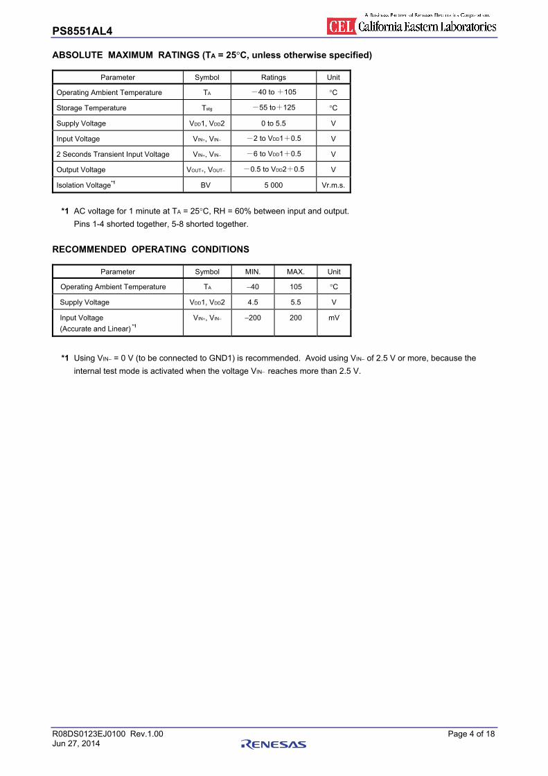
ABSOLUTE MAXIMUM RATINGS (TA = 25°C, unless otherwise specified)
Parameter Symbol Ratings Unit
Operating Ambient Temperature TA -40 to +105 °C
Storage Temperature Tstg -55 to+125 °C
Supply Voltage VDD1, VDD2 0 to 5.5 V
Input Voltage VIN+, VIN− -2 to VDD1+0.5 V
2 Seconds Transient Input Voltage VIN+, VIN− -6 to VDD1+0.5 V
Output Voltage VOUT+, VOUT− -0.5 to VDD2+0.5 V
Isolation Voltage*1 BV 5 000 Vr.m.s.
*1 AC voltage for 1 minute at TA = 25°C, RH = 60% between input and output.
Pins 1-4 shorted together, 5-8 shorted together.
RECOMMENDED OPERATING CONDITIONS
Parameter Symbol MIN. MAX. Unit
Operating Ambient Temperature TA −40 105 °C
Supply Voltage VDD1, VDD2 4.5 5.5 V
Input Voltage
(Accurate and Linear) *1
VIN+, VIN− −200 200 mV
*1 Using VIN− = 0 V (to be connected to GND1) is recommended. Avoid using VIN− of 2.5 V or more, because the
internal test mode is activated when the voltage VIN− reaches more than 2.5 V.
PS8551AL4 Chapter Title
R08DS0123EJ0100 Rev.1.00 Page 5 of 18 Jun 27, 2014
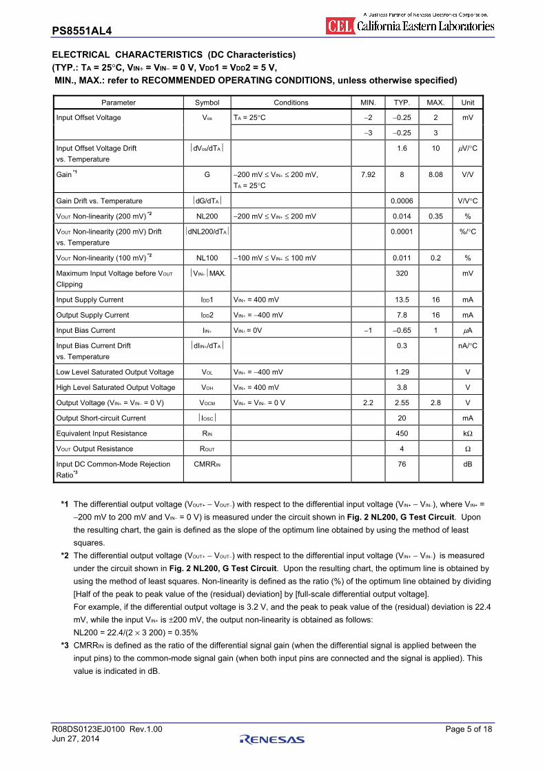
ELECTRICAL CHARACTERISTICS (DC Characteristics)
(TYP.: TA = 25°C, VIN+ = VIN− = 0 V, VDD1 = VDD2 = 5 V, MIN., MAX.: refer to RECOMMENDED OPERATING CONDITIONS, unless otherwise specified)
Parameter Symbol Conditions MIN. TYP. MAX. Unit
Input Offset Voltage Vos TA = 25°C −2 −0.25 2 mV
−3 −0.25 3
Input Offset Voltage Drift
vs. Temperature
⏐dVos/dTA⏐ 1.6 10 μV/°C
Gain *1 G −200 mV ≤ VIN+ ≤ 200 mV,
TA = 25°C7.92 8 8.08 V/V
Gain Drift vs. Temperature ⏐dG/dTA⏐ 0.0006 V/V°C
VOUT Non-linearity (200 mV) *2 NL200 −200 mV ≤ VIN+ ≤ 200 mV 0.014 0.35 %
VOUT Non-linearity (200 mV) Drift
vs. Temperature
⏐dNL200/dTA⏐ 0.0001 %/°C
VOUT Non-linearity (100 mV) *2 NL100 −100 mV ≤ VIN+ ≤ 100 mV 0.011 0.2 %
Maximum Input Voltage before VOUT
Clipping
⏐VIN+⏐MAX. 320 mV
Input Supply Current IDD1 VIN+ = 400 mV 13.5 16 mA
Output Supply Current IDD2 VIN+ = −400 mV 7.8 16 mA
Input Bias Current IIN+ VIN+ = 0V −1 −0.65 1 μA
Input Bias Current Drift
vs. Temperature
⏐dIIN+/dTA⏐ 0.3 nA/°C
Low Level Saturated Output Voltage VOL VIN+ = −400 mV 1.29 V
High Level Saturated Output Voltage VOH VIN+ = 400 mV 3.8 V
Output Voltage (VIN+ = VIN− = 0 V) VOCM VIN+ = VIN− = 0 V 2.2 2.55 2.8 V
Output Short-circuit Current ⏐IOSC⏐ 20 mA
Equivalent Input Resistance RIN 450 kΩ
VOUT Output Resistance ROUT 4 Ω
Input DC Common-Mode Rejection
Ratio*3
CMRRIN 76 dB
*1 The differential output voltage (VOUT+ − VOUT−) with respect to the differential input voltage (VIN+ − VIN−), where VIN+ =
−200 mV to 200 mV and VIN− = 0 V) is measured under the circuit shown in Fig. 2 NL200, G Test Circuit. Upon
the resulting chart, the gain is defined as the slope of the optimum line obtained by using the method of least
squares.
*2 The differential output voltage (VOUT+ − VOUT−) with respect to the differential input voltage (VIN+ − VIN−) is measured
under the circuit shown in Fig. 2 NL200, G Test Circuit. Upon the resulting chart, the optimum line is obtained by
using the method of least squares. Non-linearity is defined as the ratio (%) of the optimum line obtained by dividing
[Half of the peak to peak value of the (residual) deviation] by [full-scale differential output voltage].
For example, if the differential output voltage is 3.2 V, and the peak to peak value of the (residual) deviation is 22.4
mV, while the input VIN+ is ±200 mV, the output non-linearity is obtained as follows:
NL200 = 22.4/(2 × 3 200) = 0.35%
*3 CMRRIN is defined as the ratio of the differential signal gain (when the differential signal is applied between the
input pins) to the common-mode signal gain (when both input pins are connected and the signal is applied). This
value is indicated in dB.
PS8551AL4 Chapter Title
R08DS0123EJ0100 Rev.1.00 Page 6 of 18 Jun 27, 2014
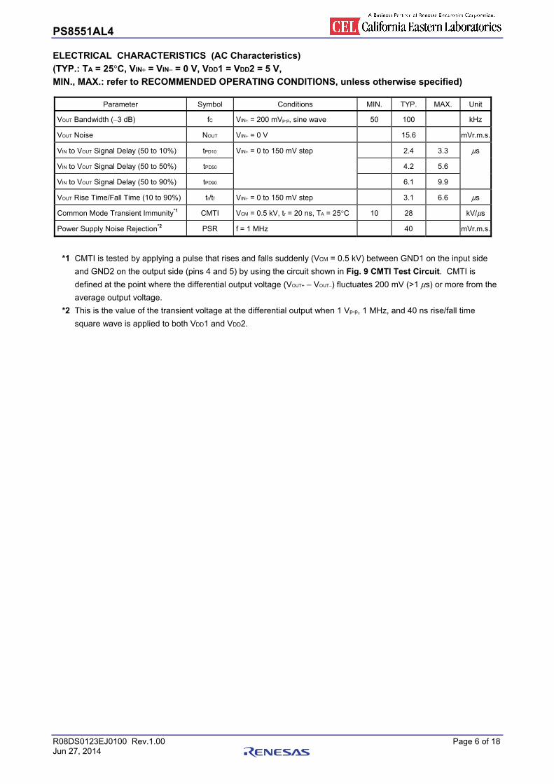
ELECTRICAL CHARACTERISTICS (AC Characteristics)
(TYP.: TA = 25°C, VIN+ = VIN− = 0 V, VDD1 = VDD2 = 5 V, MIN., MAX.: refer to RECOMMENDED OPERATING CONDITIONS, unless otherwise specified)
Parameter Symbol Conditions MIN. TYP. MAX. Unit
VOUT Bandwidth (−3 dB) fC VIN+ = 200 mVp-p, sine wave 50 100 kHz
VOUT Noise NOUT VIN+ = 0 V 15.6 mVr.m.s.
VIN to VOUT Signal Delay (50 to 10%) tPD10 VIN+ = 0 to 150 mV step 2.4 3.3 μs
VIN to VOUT Signal Delay (50 to 50%) tPD50 4.2 5.6
VIN to VOUT Signal Delay (50 to 90%) tPD90 6.1 9.9
VOUT Rise Time/Fall Time (10 to 90%) tr/tf VIN+ = 0 to 150 mV step 3.1 6.6 μs
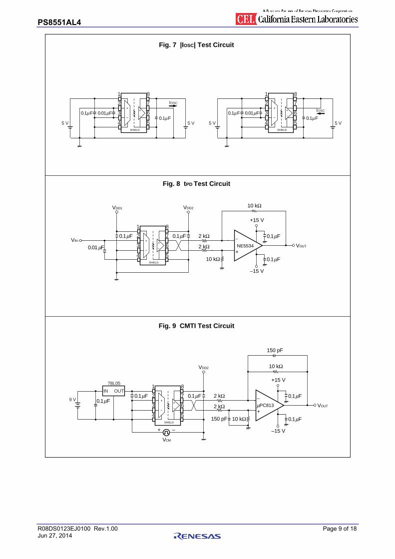
Common Mode Transient Immunity*1 CMTI VCM = 0.5 kV, tr = 20 ns, TA = 25°C 10 28 kV/μs
Power Supply Noise Rejection*2 PSR f = 1 MHz 40 mVr.m.s.
*1 CMTI is tested by applying a pulse that rises and falls suddenly (VCM = 0.5 kV) between GND1 on the input side
and GND2 on the output side (pins 4 and 5) by using the circuit shown in Fig. 9 CMTI Test Circuit. CMTI is
defined at the point where the differential output voltage (VOUT+ − VOUT−) fluctuates 200 mV (>1 μs) or more from the
average output voltage.
*2 This is the value of the transient voltage at the differential output when 1 Vp-p, 1 MHz, and 40 ns rise/fall time
square wave is applied to both VDD1 and VDD2.

PS8551AL4 Chapter Title
R08DS0123EJ0100 Rev.1.00 Page 7 of 18 Jun 27, 2014
TEST CIRCUIT
Fig. 1 VOS Test Circuit
Fig. 2 NL200, G Test Circuit
Fig. 3 IDD1 Test Circuit Fig. 4 IDD2 Test Circuit
VDD1 VDD2
10 kΩ
10 kΩ
0.1 Fμ
SHIELD
+
–
+
–
0.1 Fμ
0.47 Fμ 0.47 Fμ
VOUT
+15 V
–15 V
0.1 Fμ
0.1 FμAD624CD
(x100)
VDD1
VIN
VDD2
10 kΩ
10 kΩ
0.1 Fμ
SHIELD
+
–
+
–
0.1 Fμ
0.47 Fμ0.01 Fμ
0.47 Fμ
0.47 Fμ10 kΩ
13.2 Ω
404 Ω
+15 V
–15 V
0.1 Fμ
0.1 FμAD624CD
(x4)VOUT
+15 V
–15 V
0.1 Fμ
0.1 FμAD624CD
(x10)
1
2
3
4
8
7
6
5
1
2
3
4
8
7
6
5
0.01 Fμ
SHIELD
+
–
+
–
1
5 V
IDD1
400 mV
2
3
4
8
7
6
5
0.1 Fμ 0.01 Fμ
SHIELD
+
–
+
–
1
5 V – 400 mV
2
3
4
8
7
6
5
0.1 Fμ 0.1 Fμ
5 V
IDD2
−
+
−
+
−
+
PS8551AL4 Chapter Title
R08DS0123EJ0100 Rev.1.00 Page 8 of 18 Jun 27, 2014
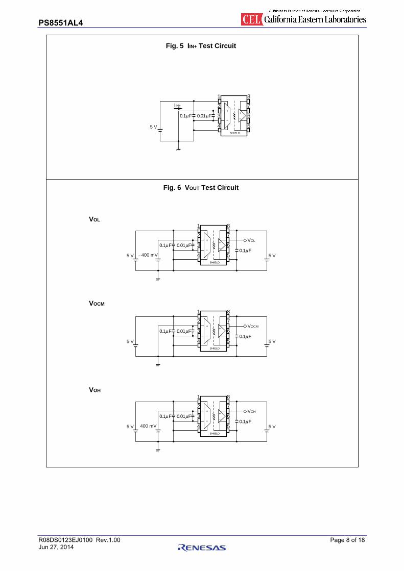
Fig. 5 IIN+ Test Circuit
Fig. 6 VOUT Test Circuit
VOL
VOCM
VOH
0.01 Fμ
SHIELD
+
–
+
–
1
– 400 mV
2
3
4
8
7
6
5
0.1 Fμ0.1 Fμ
5 V 5 V
0.01 Fμ
SHIELD
+
–
+
–
1
5 V
IIN+ 2
3
4
8
7
6
5
0.1 Fμ
VOL
0.01 Fμ
SHIELD
+
–
+
–
1
2
3
4
8
7
6
5
0.1 Fμ0.1 Fμ
5 V 5 V
VOCM
0.01 Fμ
SHIELD
+
–
+
–
1
400 mV
2
3
4
8
7
6
5
0.1 Fμ0.1 Fμ
5 V 5 V
VOH
PS8551AL4 Chapter Title
R08DS0123EJ0100 Rev.1.00 Page 9 of 18 Jun 27, 2014
Fig. 7 |IOSC| Test Circuit
Fig. 8 tPD Test Circuit
Fig. 9 CMTI Test Circuit
VDD1
VIN
VDD2
2 kΩ
10 kΩ
2 kΩ
0.1 Fμ
SHIELD
+
–
+
–
0.1 Fμ
0.01 Fμ
+15 V
–15 V
0.1 Fμ
0.1 Fμ
NE5534 VOUT
1
2
3
4
8
7
6
5
IOSC
0.01 Fμ
SHIELD
+
–
+
–
1
2
3
4
8
7
6
5
0.1 Fμ0.1 Fμ
5 V
9 V
78L05
5 V
IOSC0.01 Fμ
SHIELD
+
–
+
–
1
2
3
4
8
7
6
5
0.1 Fμ0.1 Fμ
5 V 5 V
10 kΩ
VDD2
2 kΩ
2 kΩ
0.1 Fμ0.1 Fμ
SHIELD
+
–
+
–
0.1 Fμ
PC813 VOUT
1
2
3
4
8
7
6
5
10 kΩ
150 pF
10 kΩ150 pF
IN OUT
VCM
+15 V
–15 V–+
0.1 Fμ
0.1 Fμ
μ+
−
+
−
PS8551AL4 Chapter Title
R08DS0123EJ0100 Rev.1.00 Page 10 of 18 Jun 27, 2014
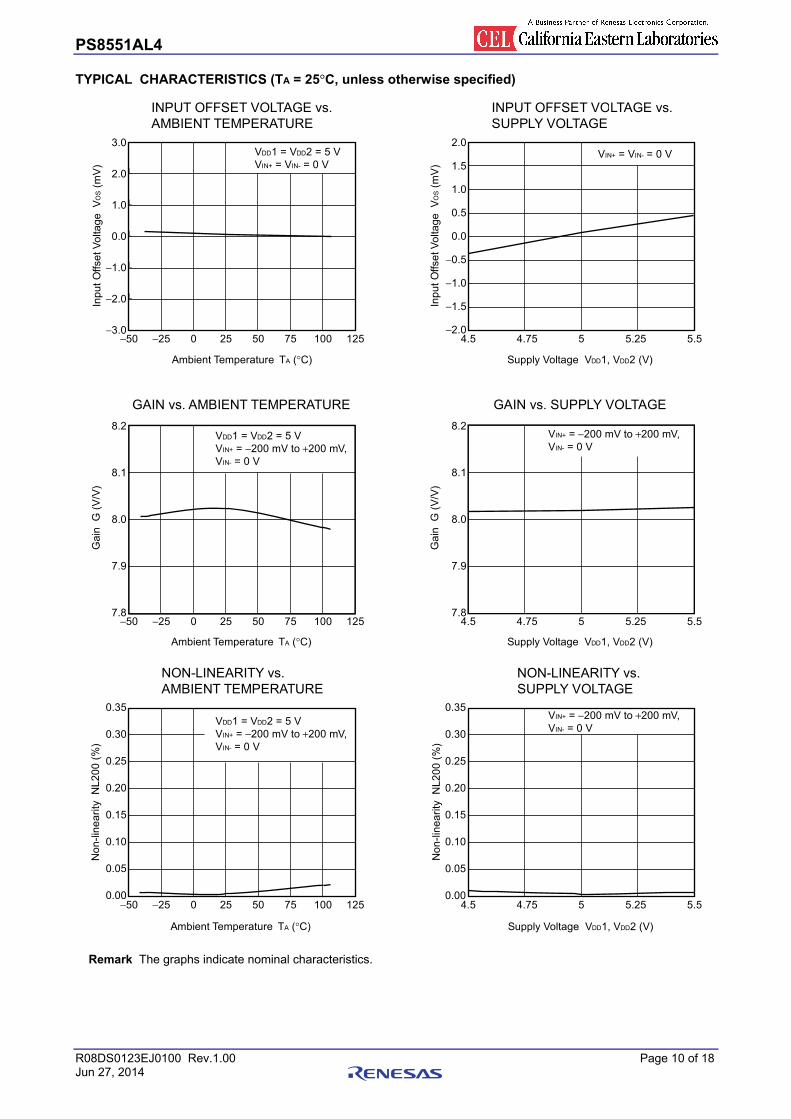
TYPICAL CHARACTERISTICS (TA = 25°C, unless otherwise specified)
3.0
�2.0
�1.0
�0.0
− �1.0
− �2.0
−3.04.5 4.75 5 5.25 5.5−50 −25 0 25 50 75 100 125
−50 −25 0 25 50 75 125100
0.35
0.30
0.25
0.20
0.15
0.10
0.05
0.00
No
n-l
ine
ari
ty
NL
20
0 (
%)
2.0
1.5
1.0
0.5
0.0
−0.5
−1.0
−1.5
−2.0
8.2
8.1
8.0
7.9
7.8
8.2
8.1
8.0
7.9
7.8
0.35
0.30
0.25
0.20
0.15
0.10
0.05
0.00
VDD1 = VDD2 = 5 VVIN+ = −200 mV to +200 mV,VIN- = 0 V
VDD1 = VDD2 = 5 VVIN+ = −200 mV to +200 mV,VIN- = 0 V
VDD1 = VDD2 = 5 VVIN+ = VIN- = 0 V
VIN+ = VIN- = 0 V
VIN+ = −200 mV to +200 mV,VIN- = 0 V
VIN+ = −200 mV to +200 mV,VIN- = 0 V
−50 −25 0 25 50 75 125100
4.5 4.75 5 5.25 5.5
4.5 4.75 5 5.25 5.5
INPUT OFFSET VOLTAGE vs.AMBIENT TEMPERATURE
Ambient Temperature TA (°C)
Inp
ut
Offs
etV
olta
ge
V
OS (
mV
)INPUT OFFSET VOLTAGE vs.SUPPLY VOLTAGE
Supply Voltage VDD1, VDD2 (V)
Inp
ut
Offs
etV
olta
ge
V
OS (
mV
)
GAIN vs. AMBIENT TEMPERATURE
Ambient Temperature TA (°C)
Ga
in
G (
V/V
)
NON-LINEARITY vs.AMBIENT TEMPERATURE
Ambient Temperature TA (°C)
No
n-l
ine
ari
ty
NL
20
0 (
%)
GAIN vs. SUPPLY VOLTAGE
Supply Voltage VDD1, VDD2 (V)
Ga
in
G (
V/V
)
NON-LINEARITY vs.SUPPLY VOLTAGE
Supply Voltage VDD1, VDD2 (V)
Remark The graphs indicate nominal characteristics.
PS8551AL4 Chapter Title
R08DS0123EJ0100 Rev.1.00 Page 11 of 18 Jun 27, 2014
4
3.5
3
2.5
2
1.5
1
4.5 4.75 5 5.25 5.5
10 100 1 000 10 000 100 000 1 000 000
Input Voltage VIN+ (V) Input Voltage VIN (V)
Frequency f (Hz)
Ou
tpu
tVo
ltag
e
VO (
V)
Su
pp
ly C
urr
en
t I D
D (
mA
)
Input Voltage VIN+ (V)
Inp
ut
Cu
rre
nt
IIN
+ (
A)
Ga
in
GV (
dB
)
Fre
qu
en
cy
fC−3
dB
(H
z)
Supply Voltage VDD1, VDD2 (V)Ambient Temperature TA (°C)
Fre
qu
en
cy
fC−3
dB
(H
z)
16
14
12
10
8
6
4
2
0
3
2
1
0
−1
−2
−3
1
0
−1
−2
−3
−4
−5
−6
−7
−8
120
100
80
60
40
20
0
120
100
80
60
40
20
0
VDD1 = VDD2 = 5 VVIN- = 0 V
VDD1 = VDD2 = 5 V,VIN- = 0 VVIN+ = 200 mVp-p sine wave
VDD1 = VDD2 = 5 V,VIN- = 0 VVIN+ = 200 mVp-p sine wave
VDD1 = VDD2 = 5 V,VIN- = 0 VVIN+ = 200 mVp-p sine wave
VDD1 = VDD2 = 5 VVDD1 = VDD2 = 5 V
VOUT+
IDD2
IDD1VOUT−
−0.4 −0.2 0 0.2 0.4−0.4 −0.2 0 0.2 0.4
−0.4 −0.2 0 0.2 0.4
125100−50 −25 0 25 7550
OUTPUT VOLTAGE vs. INPUT VOLTAGE SUPPLY CURRENT vs. INPUT VOLTAGE
INPUT CURRENT vs. INPUT VOLTAGE
FREQUENCY vs.AMBIENT TEMPERATURE
GAIN vs. FREQUENCY
FREQUENCY vs. SUPPLY VOLTAGE
μ
Remark The graphs indicate nominal characteristics.

PS8551AL4 Chapter Title
R08DS0123EJ0100 Rev.1.00 Page 12 of 18 Jun 27, 2014
7
6
5
4
3
2
1
0−50 −25 0 25 50 75 100 125
SIGNAL DELAY TIME vs.AMBIENT TEMPERATURE
Ambient Temperature TA (°C)
Sig
na
l De
lay
Tim
eP
D (
s)μ
tPD10
tf tr
tPD50
tPD90
VDD1 = VDD2 = 5 V,VIN- = 0 VVIN+ = 0 to 150 mVstep
Remark The graphs indicate nominal characteristics.
PS8551AL4 Chapter Title
R08DS0123EJ0100 Rev.1.00 Page 13 of 18 Jun 27, 2014
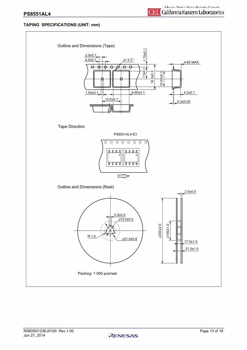
TAPING SPECIFICATIONS (UNIT: mm)
Outline and Dimensions (Tape)
1.55±0.1
2.0±0.14.0±0.1 1
.75
±0
.1
4.65 MAX.
9.95±0.1
12.0±0.1
1.5 +0.1–0
7.5±
0.1
10
.55
±0
.1
16
.0±
0.3
4.2±0.1
0.3±0.05
Outline and Dimensions (Reel)
Packing: 1 000 pcs/reel
33
0±
2.0
10
0±
1.0
2.0±0.513.0±0.2
R 1.021.0±0.8
2.0±0.5
21.5±1.0
17.5±1.0
Tape Direction
PS8551AL4-E3

PS8551AL4 Chapter Title
R08DS0123EJ0100 Rev.1.00 Page 14 of 18 Jun 27, 2014
RECOMMENDED MOUNT PAD DIMENSIONS (UNIT: mm)
D
CB
A
Part Number
PS8551AL4
Lead Bending A
lead bending type (Gull-wing)for surface mount
9.0
B
2.54
C
1.7
D
2.0

PS8551AL4 Chapter Title
R08DS0123EJ0100 Rev.1.00 Page 15 of 18 Jun 27, 2014
NOTES ON HANDLING
1. Recommended soldering conditions
(1) Infrared reflow soldering
• Peak reflow temperature 260°C or below (package surface temperature)
• Time of peak reflow temperature 10 seconds or less
• Time of temperature higher than 220°C 60 seconds or less
• Time to preheat temperature from 120 to 180°C 120±30 s
• Number of reflows Three
• Flux Rosin flux containing small amount of chlorine (The flux with a
maximum chlorine content of 0.2 Wt% is recommended.)
120±30 s(preheating)
220°C
180°C
Pac
kage
Sur
face
Tem
pera
ture
T (
°C)
Time (s)
Recommended Temperature Profile of Infrared Reflow
(heating)to 10 s
to 60 s
260°C MAX.
120°C
(2) Wave soldering
• Temperature 260°C or below (molten solder temperature)
• Time 10 seconds or less
• Preheating conditions 120°C or below (package surface temperature)
• Number of times One (Allowed to be dipped in solder including plastic mold portion.)
• Flux Rosin flux containing small amount of chlorine (The flux with a maximum chlorine content
of 0.2 Wt% is recommended.)
(3) Soldering by Soldering Iron
• Peak Temperature (lead part temperature) 350°C or below
• Time (each pins) 3 seconds or less
• Flux Rosin flux containing small amount of chlorine (The flux with a
maximum chlorine content of 0.2 Wt% is recommended.)
(a) Soldering of leads should be made at the point 1.5 to 2.0 mm from the root of the lead
PS8551AL4 Chapter Title
R08DS0123EJ0100 Rev.1.00 Page 16 of 18 Jun 27, 2014
(4) Cautions
• Fluxes
Avoid removing the residual flux with freon-based and chlorine-based cleaning solvent.
2. Cautions regarding noise
Be aware that when voltage is applied suddenly between the photocoupler’s input and output at startup, the output
transistor may enter the on state, even if the voltage is within the absolute maximum ratings.
USAGE CAUTIONS
1. This product is weak for static electricity by designed with high-speed integrated circuit so protect against static
electricity when handling.
2. Board designing
(1) By-pass capacitor of more than 0.1 μF is used between VCC and GND near device. Also, ensure that the
distance between the leads of the photocoupler and capacitor is no more than 10 mm.
(2) Keep the pattern connected the input (VIN+, VIN-) and the output (VOUT+, VOUT-), respectively, as short as possible.
(3) Do not connect any routing to the portion of the frame exposed between the pins on the package of the
photocoupler. If connected, it will affect the photocoupler's internal voltage and the photocoupler will not
operate normally.
(4) Because the maximum frequency of the signal input to the photocoupler must be lower than the allowable
frequency band, be sure to connect an anti-aliasing filter (an RC filter with R = 68 Ω and C = 0.01 μF, for
example).
(5) The signals output from the PS8551A include noise elements such as chopping noise and quantization noise
generated internally. Therefore, be sure to restrict the output frequency to the required bandwidth by adding a
low-pass filter function (an RC filter with R =10 kΩ and C = 150 pF, for example) to the operational amplifier
(post amplifier) in the next stage to the PS8551A.
(6) When the primary power supply (VDD1) is off and only the secondary power supply (VDD2) is being applied
(VDD1 = 0 V and VDD2 = 5 V), VOUT+ outputs a low level, and VOUT− outputs a high level (VOUT+ = 1.3 V TYP.,
VOUT– = 3.8 V TYP.), regardless of the input voltages (VIN+ and VIN−).
(7) The output level of VOUT+ and VOUT− might be unstable for several seconds immediately after the secondary
power supply (VDD2) is applied while the primary power supply (VDD1) is being applied.
3. Avoid storage at a high temperature and high humidity.
PS8551AL4 Chapter Title
R08DS0123EJ0100 Rev.1.00 Page 17 of 18 Jun 27, 2014
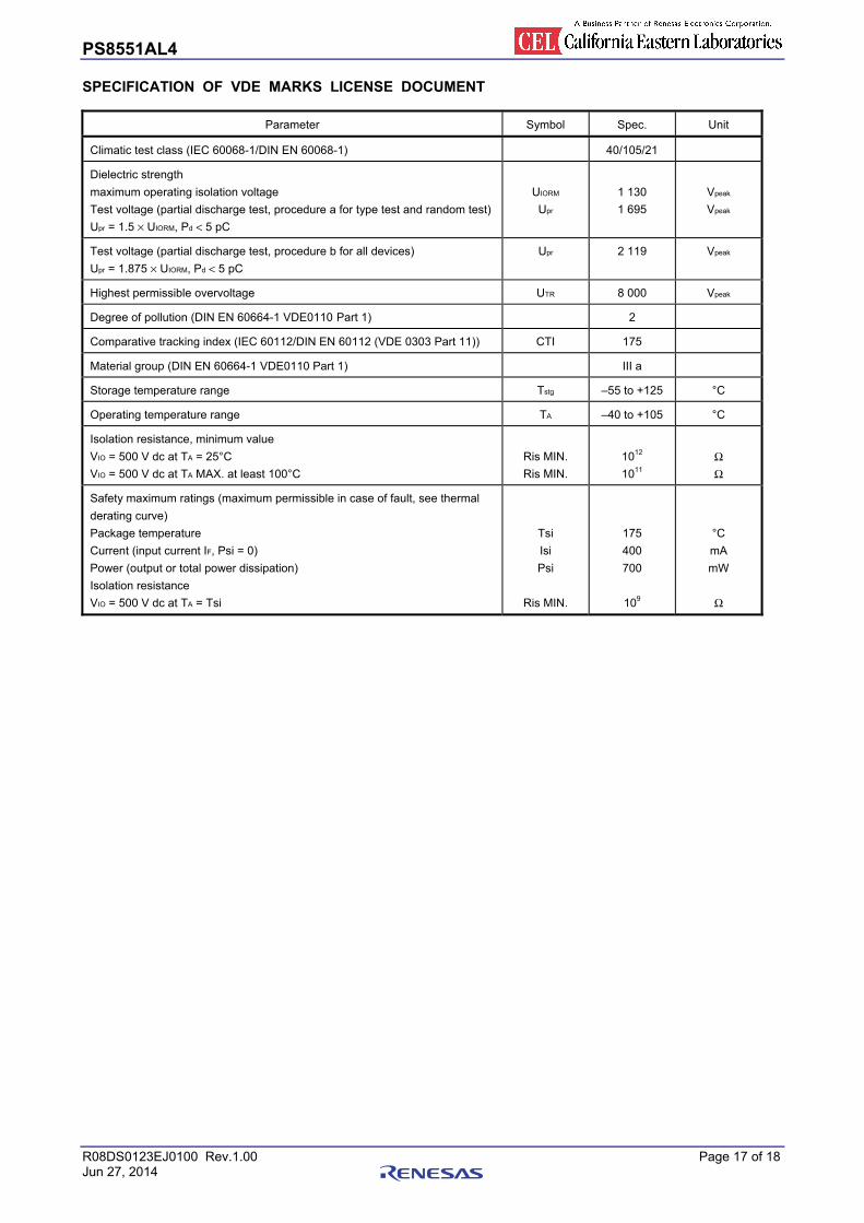
SPECIFICATION OF VDE MARKS LICENSE DOCUMENT
Parameter Symbol Spec. Unit
Climatic test class (IEC 60068-1/DIN EN 60068-1) 40/105/21
Dielectric strength
maximum operating isolation voltage
Test voltage (partial discharge test, procedure a for type test and random test)
Upr = 1.5 × UIORM, Pd < 5 pC
UIORM
Upr
1 130
1 695
Vpeak
Vpeak
Test voltage (partial discharge test, procedure b for all devices)
Upr = 1.875 × UIORM, Pd < 5 pC
Upr 2 119 Vpeak
Highest permissible overvoltage UTR 8 000 Vpeak
Degree of pollution (DIN EN 60664-1 VDE0110 Part 1) 2
Comparative tracking index (IEC 60112/DIN EN 60112 (VDE 0303 Part 11)) CTI 175
Material group (DIN EN 60664-1 VDE0110 Part 1) III a
Storage temperature range Tstg –55 to +125 °C
Operating temperature range TA –40 to +105 °C
Isolation resistance, minimum value
VIO = 500 V dc at TA = 25°C
VIO = 500 V dc at TA MAX. at least 100°C
Ris MIN.
Ris MIN.
1012
1011
Ω
Ω
Safety maximum ratings (maximum permissible in case of fault, see thermal
derating curve)
Package temperature
Current (input current IF, Psi = 0)
Power (output or total power dissipation)
Isolation resistance
VIO = 500 V dc at TA = Tsi
Tsi
Isi
Psi
Ris MIN.
175
400
700
109
°C
mA
mW
Ω
PS8551AL4 Chapter Title
R08DS0123EJ0100 Rev.1.00 Page 18 of 18 Jun 27, 2014
Caution GaAs Products This product uses gallium arsenide (GaAs). GaAs vapor and powder are hazardous to human health if inhaled or ingested, so please observe the following points.
• Follow related laws and ordinances when disposing of the product. If there are no applicable lawsand/or ordinances, dispose of the product as recommended below.
1. Commission a disposal company able to (with a license to) collect, transport and dispose ofmaterials that contain arsenic and other such industrial waste materials.
2. Exclude the product from general industrial waste and household garbage, and ensure that theproduct is controlled (as industrial waste subject to special control) up until final disposal.
• Do not burn, destroy, cut, crush, or chemically dissolve the product.
• Do not lick the product or in any way allow it to enter the mouth.
All trademarks and registered trademarks are the property of their respective owners.
C - 1
Revision History PS8551AL4 Data Sheet
Rev. Date
Description
Page Summary
1.00 Jun 27, 2014 − First edition issued

NOTICE
1. Descriptions of circuits, software and other related information in this document are provided only to illustrate the operation of semiconductor products and application examples. You are fully responsible for the incorporation of these circuits, software, and information in the design of your equipment. California Eastern Laboratories and Renesas Electronics assumes no responsibility for any losses incurred by you or third parties arising from the use of these circuits, software, or information.
2. California Eastern Laboratories has used reasonable care in preparing the information included in this document, but California Eastern Laboratories does not warrant that such information is error free. California Eastern Laboratories and Renesas Electronics assumes no liability whatsoever for any damages incurred by you resulting from errors in or omissions from the information included herein.
3. California Eastern Laboratories and Renesas Electronics do not assume any liability for infringement of patents, copyrights, or other intellectual property rights of third parties by or arising from the use of Renesas Electronics products or technical information described in this document. No license, express, implied or otherwise, is granted hereby under any patents, copyrights or other intellectual property rights of California Eastern Laboratories or Renesas Electronics or others.
4. You should not alter, modify, copy, or otherwise misappropriate any Renesas Electronics product, whether in whole or in part. California Eastern Laboratories and Renesas Electronics assume no responsibility for any losses incurred by you or third parties arising from such alteration, modification, copy or otherwise misappropriation of Renesas Electronics product.
5. Renesas Electronics products are classified according to the following two quality grades: “Standard” and “High Quality”. The recommended applications for each Renesas Electronics product depends on the product’s quality grade, as indicated below. “Standard”: Computers; office equipment; communications equipment; test and measurement equipment; audio and visual equipment; home electronic appliances; machine tools; personal electronic equipment; and industrial robots etc. “High Quality”: Transportation equipment (automobiles, trains, ships, etc.); traffic control systems; anti-disaster systems; anti-crime systems; and safety equipment etc. Renesas Electronics products are neither intended nor authorized for use in products or systems that may pose a direct threat to human life or bodily injury (artificial life support devices or systems, surgical implantations etc.), or may cause serious property damages (nuclear reactor control systems, military equipment etc.). You must check the quality grade of each Renesas Electronics product before using it in a particular application. You may not use any Renesas Electronics product for any application for which it is not intended. California Eastern Laboratories and Renesas Electronics shall not be in any way liable for any damages or losses incurred by you or third parties arising from the use of any Renesas Electronics product for which the product is not intended by California Eastern Laboratories or Renesas Electronics.
6. You should use the Renesas Electronics products described in this document within the range specified by California Eastern Laboratories, especially with respect to the maximum rating, operating supply voltage range, movement power voltage range, heat radiation characteristics, installation and other product characteristics. California Eastern Laboratories shall have no liability for malfunctions or damages arising out of the use of Renesas Electronics products beyond such specified ranges.
7. Although Renesas Electronics endeavors to improve the quality and reliability of its products, semiconductor products have specific characteristics such as the occurrence of failure at a certain rate and malfunctions under certain use conditions. Further, Renesas Electronics products are not subject to radiation resistance design. Please be sure to implement safety measures to guard them against the possibility of physical injury, and injury or damage caused by fire in the event of the failure of a Renesas Electronics product, such as safety design for hardware and software including but not limited to redundancy, fire control and malfunction prevention, appropriate treatment for aging degradation or any other appropriate measures. Because the evaluation of microcomputer software alone is very difficult, please evaluate the safety of the final products or systems manufactured by you.
8. Please contact a California Eastern Laboratories sales office for details as to environmental matters such as the environmental compatibility of each Renesas Electronics product. Please use Renesas Electronics products in compliance with all applicable laws and regulations that regulate the inclusion or use of controlled substances, including without limitation, the EU RoHS Directive. California Eastern Laboratories and Renesas Electronics assume no liability for damages or losses occurring as a result of your noncompliance with applicable laws and regulations.
9. Renesas Electronics products and technology may not be used for or incorporated into any products or systems whose manufacture, use, or sale is prohibited under any applicable domestic or foreign laws or regulations. You should not use Renesas Electronics products or technology described in this document for any purpose relating to military applications or use by the military, including but not limited to the development of weapons of mass destruction. When exporting the Renesas Electronics products or technology described in this document, you should comply with the applicable export control laws and regulations and follow the procedures required by such laws and regulations.
10. It is the responsibility of the buyer or distributor of California Eastern Laboratories, who distributes, disposes of, or otherwise places the Renesas Electronics product with a third party, to notify such third party in advance of the contents and conditions set forth in this document, California Eastern Laboratories and Renesas Electronics assume no responsibility for any losses incurred by you or third parties as a result of unauthorized use of Renesas Electronics products.
11. This document may not be reproduced or duplicated in any form, in whole or in part, without prior written consent of California Eastern Laboratories.12. Please contact a California Eastern Laboratories sales office if you have any questions regarding the information contained in this document or Renesas
Electronics products, or if you have any other inquiries.
NOTE 1: “Renesas Electronics” as used in this document means Renesas Electronics Corporation and also includes its majority-owned subsidiaries.NOTE 2: “Renesas Electronics product(s)” means any product developed or manufactured by or for Renesas Electronics.NOTE 3: Products and product information are subject to change without notice.
CEL Headquarters • 4590 Patrick Henry Drive, Santa Clara, CA 95054 • Phone (408) 919-2500 • www.cel.com
For a complete list of sales offices, representatives and distributors,Please visit our website: www.cel.com/contactus