R Board Routability Guidelines with Xilinx Fine-Pitch …bmc.bu.edu/bmc/asd/tester/xapp157.pdf · 2...
8
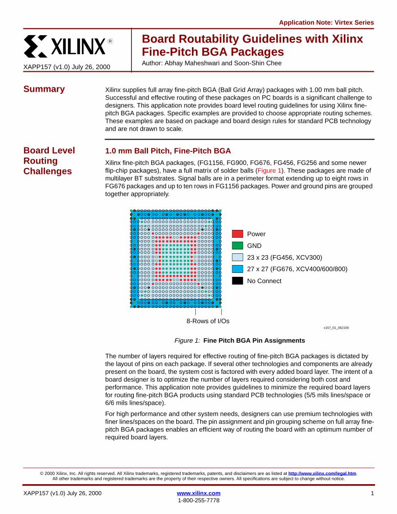
XAPP157 (v1.0) July 26, 2000 www .xilinx.com 1 1-800-255-7778 © 2000 Xilinx, Inc. All rights reserved. All Xilinx trademarks, registered trademarks, patents, and disclaimers are as listed at http://www .xilinx.com/legal.htm. All other trademarks and registered trademarks are the property of their respective owners. All specifications are subject to change without notice. Summary Xilinx supplies full array fine-pitch BGA (Ball Grid Array) packages with 1.00 mm ball pitch. Successful and effective routing of these packages on PC boards is a significant challenge to designers. This application note provides board level routing guidelines for using Xilinx fine- pitch BGA packages. Specific examples are provided to choose appropriate routing schemes. These examples are based on package and board design rules for standard PCB technology and are not drawn to scale. Board Level Routing Challenges 1.0 mm Ball Pitch, Fine-Pitch BGA Xilinx fine-pitch BGA packages, (FG1156, FG900, FG676, FG456, FG256 and some newer flip-chip packages), have a full matrix of solder balls (Figure 1). These packages are made of multilayer BT substrates. Signal balls are in a perimeter format extending up to eight rows in FG676 packages and up to ten rows in FG1156 packages. Power and ground pins are grouped together appropriately. The number of layers required for effective routing of fine-pitch BGA packages is dictated by the layout of pins on each package. If several other technologies and components are already present on the board, the system cost is factored with every added board layer. The intent of a board designer is to optimize the number of layers required considering both cost and performance. This application note provides guidelines to minimize the required board layers for routing fine-pitch BGA products using standard PCB technologies (5/5 mils lines/space or 6/6 mils lines/space). For high performance and other system needs, designers can use premium technologies with finer lines/spaces on the board. The pin assignment and pin grouping scheme on full array fine- pitch BGA packages enables an efficient way of routing the board with an optimum number of required board layers. Application Note: Virtex Series XAPP157 (v1.0) July 26, 2000 Board Routability Guidelines with Xilinx Fine-Pitch BGA Packages Author: Abhay Maheshwari and Soon-Shin Chee R Figure 1: Fine Pitch BGA Pin Assignments x157_01_062100 8-Rows of I/Os 27 x 27 (FG676, XCV400/600/800) 23 x 23 (FG456, XCV300) Power No Connect GND
Transcript of R Board Routability Guidelines with Xilinx Fine-Pitch …bmc.bu.edu/bmc/asd/tester/xapp157.pdf · 2...
Summary Xilinx supplies full array fine-pitch BGA (Ball Grid Array) packages with 100 mm ball pitchSuccessful and effective routing of these packages on PC boards is a significant challenge todesigners This application note provides board level routing guidelines for using Xilinx fine-pitch BGA packages Specific examples are provided to choose appropriate routing schemesThese examples are based on package and board design rules for standard PCB technologyand are not drawn to scale
Board LevelRoutingChallenges
10 mm Ball Pitch Fine-Pitch BGAXilinx fine-pitch BGA packages (FG1156 FG900 FG676 FG456 FG256 and some newerflip-chip packages) have a full matrix of solder balls (Figure 1) These packages are made ofmultilayer BT substrates Signal balls are in a perimeter format extending up to eight rows inFG676 packages and up to ten rows in FG1156 packages Power and ground pins are groupedtogether appropriately
The number of layers required for effective routing of fine-pitch BGA packages is dictated bythe layout of pins on each package If several other technologies and components are alreadypresent on the board the system cost is factored with every added board layer The intent of aboard designer is to optimize the number of layers required considering both cost andperformance This application note provides guidelines to minimize the required board layersfor routing fine-pitch BGA products using standard PCB technologies (55 mils linesspace or66 mils linesspace)
For high performance and other system needs designers can use premium technologies withfiner linesspaces on the board The pin assignment and pin grouping scheme on full array fine-pitch BGA packages enables an efficient way of routing the board with an optimum number ofrequired board layers
Application Note Virtex Series
XAPP157 (v10) July 26 2000
Board Routability Guidelines with XilinxFine-Pitch BGA PackagesAuthor Abhay Maheshwari and Soon-Shin Chee
R13
Figure 1 Fine Pitch BGA Pin Assignments
x157_01_062100
8-Rows of IOs
27 x 27 (FG676 XCV400600800)
23 x 23 (FG456 XCV300)
Power
No Connect
GND
XAPP157 (v10) July 26 2000 wwwxilinxcom 11-800-255-7778
copy 2000 Xilinx Inc All rights reserved All Xilinx trademarks registered trademarks patents and disclaimers are as listed at httpwww xilinxcomlegalhtm All other trademarks and registered trademarks are the property of their respective owners All specifications are subject to change without notice
Board Routability Guidelines with Xilinx Fine-Pitch BGA PackagesR13
Board RoutingStrategy
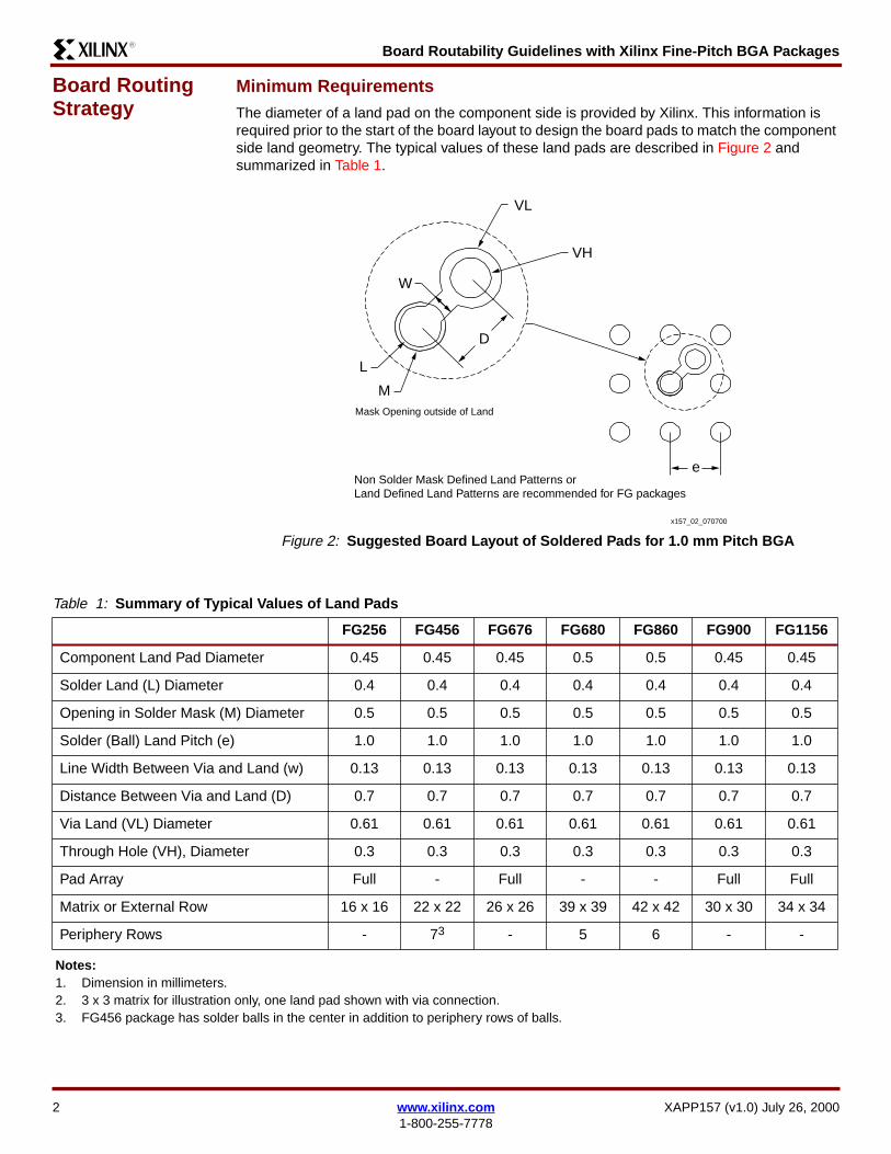
Minimum RequirementsThe diameter of a land pad on the component side is provided by Xilinx This information isrequired prior to the start of the board layout to design the board pads to match the componentside land geometry The typical values of these land pads are described in Figure 2 andsummarized in Table 1
Figure 2 Suggested Board Layout of Soldered Pads for 10 mm Pitch BGA
x157_02_070700
Non Solder Mask Defined Land Patterns or13Land Defined Land Patterns are recommended for FG packages
Mask Opening outside of Land
VL
VH
e
D
W
M
L
Table 1 Summary of Typical Values of Land Pads
FG256 FG456 FG676 FG680 FG860 FG900 FG1156
Component Land Pad Diameter 045 045 045 05 05 045 045
Solder Land (L) Diameter 04 04 04 04 04 04 04
Opening in Solder Mask (M) Diameter 05 05 05 05 05 05 05
Solder (Ball) Land Pitch (e) 10 10 10 10 10 10 10
Line Width Between Via and Land (w) 013 013 013 013 013 013 013
Distance Between Via and Land (D) 07 07 07 07 07 07 07
Via Land (VL) Diameter 061 061 061 061 061 061 061
Through Hole (VH) Diameter 03 03 03 03 03 03 03
Pad Array Full - Full - - Full Full
Matrix or External Row 16 x 16 22 x 22 26 x 26 39 x 39 42 x 42 30 x 30 34 x 34
Periphery Rows - 73 - 5 6 - -
Notes1 Dimension in millimeters2 3 x 3 matrix for illustration only one land pad shown with via connection3 FG456 package has solder balls in the center in addition to periphery rows of balls
2 wwwxilinxcom XAPP157 (v10) July 26 20001-800-255-7778
Board Routability Guidelines with Xilinx Fine-Pitch BGA PackagesR13
For FG series packages NSMD (Non Solder Mask Defined) pads on the board are suggestedThis allows a clearance between the land metal (diameter L) and the solder mask opening(diameter M) as shown in Figure 2 The space between the NSMD pad and the solder maskand the actual signal trace widths depends on the capability of the PCB vendor The cost of thePCB is higher when the line width and spaces are smaller
Selection of the pad types and pad sizes determines the available space between adjacentballs for signal escape Based on PCB capability the number of lines that can share theavailable space is described in Figure 3 Based on geometrical considerations if one signalescapes between adjacent balls then two signal rows can be routed on a single metal layerThis is illustrated in Figure 3 as routing with one linechannel either at 6 mils lines and spacesor 5 mils lines and spaces Using this suggested routing scheme a minimum of eight PCBlayers are required to route 10 signal rows in a package
A slightly lower trace width can be used by the inner signal rows routed in internal layers thanthe top and bottom external or exposed traces Depending on the signal being handled thepractice of necking down a trace in the critical space between the BGA balls is allowableChanges in width over very short distances can cause small impedance changes Validatethese issues with the board vendor and signal integrity engineers responsible for design
Figure 3 FG676 PC Board LayoutLand Pattern
x157_03_061300
1-LineChannel135 mils Line 5 mils Spacing13
(Standard Technology)13
1-LineChannel136 mils Line 6 mils Spacing13
(Standard Technology)13
O030 mm (0012)
O061 mm (0024)
O05 mm (0020)
O04 mm (0016) Detail A
IO
GNDPWR
VCCINT
27 x 27 mm 10 mm Fine Pitch BGA
PCB Design Rule (10 mm Ball Pitch)Lines PerChannel13
PCBLayer13
BallPad13
ViaPad13
1
TraceWidthSpacing (mils)
55
IORows
8 6 016 024
10 mm 10 mm
(93 mils)gt5 mils
(88 mils)gt5 mils
5 mils
6 mils
Detail A
Signal(L1)
Signal(L2)
Signal(L3)
Signal(L4)
PWRPlane
GNDPlane
XAPP157 (v10) July 26 2000 wwwxilinxcom 31-800-255-7778
Board Routability Guidelines with Xilinx Fine-Pitch BGA PackagesR13
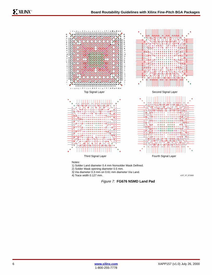
Figure 3 describes a board-level layout strategy for a Xilinx 10 mm pitch FG676 packageDetail A in Figure 3 describes the opening geometry for the Land Pad and the Solder MaskRouting with 5 mils linestrace allows one signal per channel (between the balls) Forsuccessful routing eight row deep signal traces require six PCB layers Figure 4 shows thesuggested schematic of layers for the six-layer routing scheme
Using premium board technology such as Microvia Technology (allowing up to 4 mils lines andspaces) efficient routing is possible with a reduced number of board layers A grouping schemefor power ground control and IO pins may also enable efficient routing
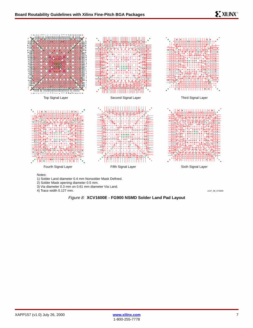
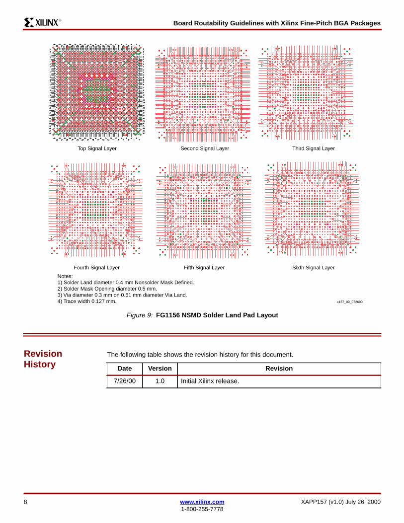
Figure 5 through 9 are drawings of suggested layer-by-layer board routing for the FG series256 456 676 900 and 1156 packages These drawings assume the standard PCB technologyof 5 mils lines and spaces
Figure 4 Six-Layer Routing Scheme
Figure 5 FG256 NSMD Land Pad
L - 213
L - 313
L - 413
L - 513
L - 613
L - 113Signal
PowerGnd
Signal
Signal
PowerGnd
Signalx157_04_051800
x157_05_072600
First Signal Layer Second Signal Layer
Notes131) Solder Land diameter 04 mm Nonsolder Mask Defined132) Solder Mask Opening diameter 05 mm133) Via diameter 03 mm on 061 mm diameter Via Land134) Trace width 0127 mm
4 wwwxilinxcom XAPP157 (v10) July 26 20001-800-255-7778
Board Routability Guidelines with Xilinx Fine-Pitch BGA PackagesR13
Figure 6 FG456 NSMD Land Pad
x157_06_072600
Second Signal LayerFirst Signal Layer
Third Signal Layer
Notes131) Solder land diameter 04 mm Nonsolder Mask Defined132) Solder Mask Opening 05 mm diameter133) Via diameter 03 mm on 061 mm diameter Via Land134) All Layers trace width 0127 mm
XAPP157 (v10) July 26 2000 wwwxilinxcom 51-800-255-7778
Board Routability Guidelines with Xilinx Fine-Pitch BGA PackagesR13
Figure 7 FG676 NSMD Land Pad
x157_07_072600
Top Signal Layer Second Signal Layer
Third Signal Layer Fourth Signal Layer
Notes131) Solder Land diameter 04 mm Nonsolder Mask Defined132) Solder Mask opening diameter 05 mm133) Via diameter 03 mm on 061 mm diameter Via Land134) Trace width 0127 mm
6 wwwxilinxcom XAPP157 (v10) July 26 20001-800-255-7778
Board Routability Guidelines with Xilinx Fine-Pitch BGA PackagesR13
Figure 8 XCV1600E - FG900 NSMD Solder Land Pad Layout
Notes131) Solder Land diameter 04 mm Nonsolder Mask Defined132) Solder Mask opening diameter 05 mm133) Via diameter 03 mm on 061 mm diameter Via Land134) Trace width 0127 mm
Sixth Signal LayerFifth Signal LayerFourth Signal Layer
Third Signal LayerSecond Signal LayerTop Signal Layer
x157_08_072600
XAPP157 (v10) July 26 2000 wwwxilinxcom 71-800-255-7778
Board Routability Guidelines with Xilinx Fine-Pitch BGA PackagesR13
RevisionHistory
The following table shows the revision history for this document
Figure 9 FG1156 NSMD Solder Land Pad Layout
x157_09_072600
Fourth Signal Layer Fifth Signal Layer Sixth Signal Layer
Top Signal Layer Second Signal Layer Third Signal Layer
Notes131) Solder Land diameter 04 mm Nonsolder Mask Defined132) Solder Mask Opening diameter 05 mm133) Via diameter 03 mm on 061 mm diameter Via Land134) Trace width 0127 mm
Date Version Revision
72600 10 Initial Xilinx release
8 wwwxilinxcom XAPP157 (v10) July 26 20001-800-255-7778
- Summary
- Board Level Routing Challenges
-
- 10 mm Ball Pitch Fine-Pitch BGA
-
- Board Routing Strategy
-
- Minimum Requirements
-
- Revision History
-
Board Routability Guidelines with Xilinx Fine-Pitch BGA PackagesR13
Board RoutingStrategy
Minimum RequirementsThe diameter of a land pad on the component side is provided by Xilinx This information isrequired prior to the start of the board layout to design the board pads to match the componentside land geometry The typical values of these land pads are described in Figure 2 andsummarized in Table 1
Figure 2 Suggested Board Layout of Soldered Pads for 10 mm Pitch BGA
x157_02_070700
Non Solder Mask Defined Land Patterns or13Land Defined Land Patterns are recommended for FG packages
Mask Opening outside of Land
VL
VH
e
D
W
M
L
Table 1 Summary of Typical Values of Land Pads
FG256 FG456 FG676 FG680 FG860 FG900 FG1156
Component Land Pad Diameter 045 045 045 05 05 045 045
Solder Land (L) Diameter 04 04 04 04 04 04 04
Opening in Solder Mask (M) Diameter 05 05 05 05 05 05 05
Solder (Ball) Land Pitch (e) 10 10 10 10 10 10 10
Line Width Between Via and Land (w) 013 013 013 013 013 013 013
Distance Between Via and Land (D) 07 07 07 07 07 07 07
Via Land (VL) Diameter 061 061 061 061 061 061 061
Through Hole (VH) Diameter 03 03 03 03 03 03 03
Pad Array Full - Full - - Full Full
Matrix or External Row 16 x 16 22 x 22 26 x 26 39 x 39 42 x 42 30 x 30 34 x 34
Periphery Rows - 73 - 5 6 - -
Notes1 Dimension in millimeters2 3 x 3 matrix for illustration only one land pad shown with via connection3 FG456 package has solder balls in the center in addition to periphery rows of balls
2 wwwxilinxcom XAPP157 (v10) July 26 20001-800-255-7778
Board Routability Guidelines with Xilinx Fine-Pitch BGA PackagesR13
For FG series packages NSMD (Non Solder Mask Defined) pads on the board are suggestedThis allows a clearance between the land metal (diameter L) and the solder mask opening(diameter M) as shown in Figure 2 The space between the NSMD pad and the solder maskand the actual signal trace widths depends on the capability of the PCB vendor The cost of thePCB is higher when the line width and spaces are smaller
Selection of the pad types and pad sizes determines the available space between adjacentballs for signal escape Based on PCB capability the number of lines that can share theavailable space is described in Figure 3 Based on geometrical considerations if one signalescapes between adjacent balls then two signal rows can be routed on a single metal layerThis is illustrated in Figure 3 as routing with one linechannel either at 6 mils lines and spacesor 5 mils lines and spaces Using this suggested routing scheme a minimum of eight PCBlayers are required to route 10 signal rows in a package
A slightly lower trace width can be used by the inner signal rows routed in internal layers thanthe top and bottom external or exposed traces Depending on the signal being handled thepractice of necking down a trace in the critical space between the BGA balls is allowableChanges in width over very short distances can cause small impedance changes Validatethese issues with the board vendor and signal integrity engineers responsible for design
Figure 3 FG676 PC Board LayoutLand Pattern
x157_03_061300
1-LineChannel135 mils Line 5 mils Spacing13
(Standard Technology)13
1-LineChannel136 mils Line 6 mils Spacing13
(Standard Technology)13
O030 mm (0012)
O061 mm (0024)
O05 mm (0020)
O04 mm (0016) Detail A
IO
GNDPWR
VCCINT
27 x 27 mm 10 mm Fine Pitch BGA
PCB Design Rule (10 mm Ball Pitch)Lines PerChannel13
PCBLayer13
BallPad13
ViaPad13
1
TraceWidthSpacing (mils)
55
IORows
8 6 016 024
10 mm 10 mm
(93 mils)gt5 mils
(88 mils)gt5 mils
5 mils
6 mils
Detail A
Signal(L1)
Signal(L2)
Signal(L3)
Signal(L4)
PWRPlane
GNDPlane
XAPP157 (v10) July 26 2000 wwwxilinxcom 31-800-255-7778
Board Routability Guidelines with Xilinx Fine-Pitch BGA PackagesR13
Figure 3 describes a board-level layout strategy for a Xilinx 10 mm pitch FG676 packageDetail A in Figure 3 describes the opening geometry for the Land Pad and the Solder MaskRouting with 5 mils linestrace allows one signal per channel (between the balls) Forsuccessful routing eight row deep signal traces require six PCB layers Figure 4 shows thesuggested schematic of layers for the six-layer routing scheme
Using premium board technology such as Microvia Technology (allowing up to 4 mils lines andspaces) efficient routing is possible with a reduced number of board layers A grouping schemefor power ground control and IO pins may also enable efficient routing
Figure 5 through 9 are drawings of suggested layer-by-layer board routing for the FG series256 456 676 900 and 1156 packages These drawings assume the standard PCB technologyof 5 mils lines and spaces
Figure 4 Six-Layer Routing Scheme
Figure 5 FG256 NSMD Land Pad
L - 213
L - 313
L - 413
L - 513
L - 613
L - 113Signal
PowerGnd
Signal
Signal
PowerGnd
Signalx157_04_051800
x157_05_072600
First Signal Layer Second Signal Layer
Notes131) Solder Land diameter 04 mm Nonsolder Mask Defined132) Solder Mask Opening diameter 05 mm133) Via diameter 03 mm on 061 mm diameter Via Land134) Trace width 0127 mm
4 wwwxilinxcom XAPP157 (v10) July 26 20001-800-255-7778
Board Routability Guidelines with Xilinx Fine-Pitch BGA PackagesR13
Figure 6 FG456 NSMD Land Pad
x157_06_072600
Second Signal LayerFirst Signal Layer
Third Signal Layer
Notes131) Solder land diameter 04 mm Nonsolder Mask Defined132) Solder Mask Opening 05 mm diameter133) Via diameter 03 mm on 061 mm diameter Via Land134) All Layers trace width 0127 mm
XAPP157 (v10) July 26 2000 wwwxilinxcom 51-800-255-7778
Board Routability Guidelines with Xilinx Fine-Pitch BGA PackagesR13
Figure 7 FG676 NSMD Land Pad
x157_07_072600
Top Signal Layer Second Signal Layer
Third Signal Layer Fourth Signal Layer
Notes131) Solder Land diameter 04 mm Nonsolder Mask Defined132) Solder Mask opening diameter 05 mm133) Via diameter 03 mm on 061 mm diameter Via Land134) Trace width 0127 mm
6 wwwxilinxcom XAPP157 (v10) July 26 20001-800-255-7778
Board Routability Guidelines with Xilinx Fine-Pitch BGA PackagesR13
Figure 8 XCV1600E - FG900 NSMD Solder Land Pad Layout
Notes131) Solder Land diameter 04 mm Nonsolder Mask Defined132) Solder Mask opening diameter 05 mm133) Via diameter 03 mm on 061 mm diameter Via Land134) Trace width 0127 mm
Sixth Signal LayerFifth Signal LayerFourth Signal Layer
Third Signal LayerSecond Signal LayerTop Signal Layer
x157_08_072600
XAPP157 (v10) July 26 2000 wwwxilinxcom 71-800-255-7778
Board Routability Guidelines with Xilinx Fine-Pitch BGA PackagesR13
RevisionHistory
The following table shows the revision history for this document
Figure 9 FG1156 NSMD Solder Land Pad Layout
x157_09_072600
Fourth Signal Layer Fifth Signal Layer Sixth Signal Layer
Top Signal Layer Second Signal Layer Third Signal Layer
Notes131) Solder Land diameter 04 mm Nonsolder Mask Defined132) Solder Mask Opening diameter 05 mm133) Via diameter 03 mm on 061 mm diameter Via Land134) Trace width 0127 mm
Date Version Revision
72600 10 Initial Xilinx release
8 wwwxilinxcom XAPP157 (v10) July 26 20001-800-255-7778
- Summary
- Board Level Routing Challenges
-
- 10 mm Ball Pitch Fine-Pitch BGA
-
- Board Routing Strategy
-
- Minimum Requirements
-
- Revision History
-

Board Routability Guidelines with Xilinx Fine-Pitch BGA PackagesR13
Figure 6 FG456 NSMD Land Pad
x157_06_072600
Second Signal LayerFirst Signal Layer
Third Signal Layer
Notes131) Solder land diameter 04 mm Nonsolder Mask Defined132) Solder Mask Opening 05 mm diameter133) Via diameter 03 mm on 061 mm diameter Via Land134) All Layers trace width 0127 mm
XAPP157 (v10) July 26 2000 wwwxilinxcom 51-800-255-7778
Board Routability Guidelines with Xilinx Fine-Pitch BGA PackagesR13
Figure 7 FG676 NSMD Land Pad
x157_07_072600
Top Signal Layer Second Signal Layer
Third Signal Layer Fourth Signal Layer
Notes131) Solder Land diameter 04 mm Nonsolder Mask Defined132) Solder Mask opening diameter 05 mm133) Via diameter 03 mm on 061 mm diameter Via Land134) Trace width 0127 mm
6 wwwxilinxcom XAPP157 (v10) July 26 20001-800-255-7778
Board Routability Guidelines with Xilinx Fine-Pitch BGA PackagesR13
Figure 8 XCV1600E - FG900 NSMD Solder Land Pad Layout
Notes131) Solder Land diameter 04 mm Nonsolder Mask Defined132) Solder Mask opening diameter 05 mm133) Via diameter 03 mm on 061 mm diameter Via Land134) Trace width 0127 mm
Sixth Signal LayerFifth Signal LayerFourth Signal Layer
Third Signal LayerSecond Signal LayerTop Signal Layer
x157_08_072600
XAPP157 (v10) July 26 2000 wwwxilinxcom 71-800-255-7778
Board Routability Guidelines with Xilinx Fine-Pitch BGA PackagesR13
RevisionHistory
The following table shows the revision history for this document
Figure 9 FG1156 NSMD Solder Land Pad Layout
x157_09_072600
Fourth Signal Layer Fifth Signal Layer Sixth Signal Layer
Top Signal Layer Second Signal Layer Third Signal Layer
Notes131) Solder Land diameter 04 mm Nonsolder Mask Defined132) Solder Mask Opening diameter 05 mm133) Via diameter 03 mm on 061 mm diameter Via Land134) Trace width 0127 mm
Date Version Revision
72600 10 Initial Xilinx release
8 wwwxilinxcom XAPP157 (v10) July 26 20001-800-255-7778
- Summary
- Board Level Routing Challenges
-
- 10 mm Ball Pitch Fine-Pitch BGA
-
- Board Routing Strategy
-
- Minimum Requirements
-
- Revision History
-
Board Routability Guidelines with Xilinx Fine-Pitch BGA PackagesR13
RevisionHistory
The following table shows the revision history for this document
Figure 9 FG1156 NSMD Solder Land Pad Layout
x157_09_072600
Fourth Signal Layer Fifth Signal Layer Sixth Signal Layer
Top Signal Layer Second Signal Layer Third Signal Layer
Notes131) Solder Land diameter 04 mm Nonsolder Mask Defined132) Solder Mask Opening diameter 05 mm133) Via diameter 03 mm on 061 mm diameter Via Land134) Trace width 0127 mm
Date Version Revision
72600 10 Initial Xilinx release
8 wwwxilinxcom XAPP157 (v10) July 26 20001-800-255-7778
- Summary
- Board Level Routing Challenges
-
- 10 mm Ball Pitch Fine-Pitch BGA
-
- Board Routing Strategy
-
- Minimum Requirements
-
- Revision History
-
![charliep Nokia Research Center [seamoby] · RR Protocol Overview • Test return routability for home address (HoTI, HoT) • Test return routability for care-of address (CoTI, CoT)](https://static.fdocuments.in/doc/165x107/5fbf2901fd532c53d67809c9/charliep-nokia-research-center-seamoby-rr-protocol-overview-a-test-return-routability.jpg)