qwitt diode analysis
19
Page 380 First Internati1,a1 Symposium on Space Terahertz Technology QUANTUM WELL AND QUANTUM BARRIER DIODES FOR GENERATING SUB-MILLIMETER WAVE POWER. Hans GrOnqvist*, Erik Kollberg* and Anders Rydberg**. The Millimeter Wave Laboratory Departments of Applied Electron Physics* & Radio and Space Science** Chalmers University of Technology 5-412 96 Goteborg, Sweden Abstract. Quantum well diodes have been used for generating power at millimeter and submillimeter waves, both in negative resistance oscillators and in multipliers. In this paper, we will first discuss the power versus frequency and the maximum frequency of oscillation of "ordinary" quantum well oscillators. Possible methods of improving the power output and the maximum frequency of oscilla- tion will be suggested. Quantum well diode multipliers will also be discussed. Realizing the impor- tance of the non-linear capacitance for the quantum well diode multiplier efficiency we have investi- gated a quantum barrier diode in multiplier applications. 1. Introduction. Quantum Well diode (QW-diode) oscillators have recently been shown to have a potential to generate power in the millimeter and submillimeter wave region [1,2]. The device used in these oscillators is a kind of tunnel diode with negative differential resistance, first suggested as early as 1970 by Esaki. They were, however, not implemented experimentally until 1974, [3], when MBE ( Molecular Beam submillimeter) technique for making appropriately doped epitaxial Ga(ADAs was developed. The first experiments with QW diode oscillators were made by Sollner 1983 at microwave frequencies. The best QW oscillator results so far have been reported by Sollner et. al. [1] and by us [2]. The QW-diode can also be used in multipliers [4], and should have a possible application in negative resistance mixers with a potential of having conversion gain [5]. In paragraph 11 we will describe a new device, the Quantum Barrier Varactor (QBV) diode multiplier, which has high efficiency and interesting properties since only odd harmonics are created. 2. Device design. A typical outline of a QW-diode is shown in Fig. 1. The doping profile and the band bending for a biased diode is shown in Fig. 2a. The tunneling current has a maximum for the bias voltage making the energy level in the well equal in energy with the Fermi level to the left of the QW. An approximate equivalent circuit of the QW-diode is shown in Fig. 2b. The parameters in the equivalent circuit are depending on the doping profile, bias conditions, and size of the diode. There are several possibilities to increase the output power. It has been suggested that more power will be available if the AI-AV product (Al and AV are the differences in current and voltage respectively, measured
-
Upload
aghna-tiyas-mandal -
Category
Documents
-
view
224 -
download
0
description
Gunn diode ,qwitt diode , useful analysis , microwave solid state devices.
Transcript of qwitt diode analysis
Page 380 First Internati1,a1 Symposium on Space Terahertz Technology
QUANTUM WELL AND QUANTUM BARRIER DIODES FOR GENERATINGSUB-MILLIMETER WAVE POWER.
Hans GrOnqvist*, Erik Kollberg* and Anders Rydberg**.
The Millimeter Wave Laboratory
Departments of Applied Electron Physics* & Radio and Space Science**
Chalmers University of Technology
5-412 96 Goteborg, Sweden
Abstract.
Quantum well diodes have been used for generating power at millimeter and submillimeter
waves, both in negative resistance oscillators and in multipliers. In this paper, we will first discuss
the power versus frequency and the maximum frequency of oscillation of "ordinary" quantum well
oscillators. Possible methods of improving the power output and the maximum frequency of oscilla-
tion will be suggested. Quantum well diode multipliers will also be discussed. Realizing the impor-
tance of the non-linear capacitance for the quantum well diode multiplier efficiency we have investi-
gated a quantum barrier diode in multiplier applications.
1. Introduction.
Quantum Well diode (QW-diode) oscillators have recently been shown to have a potential to
generate power in the millimeter and submillimeter wave region [1,2]. The device used in these
oscillators is a kind of tunnel diode with negative differential resistance, first suggested as early as
1970 by Esaki. They were, however, not implemented experimentally until 1974, [3], when MBE
(Molecular Beam submillimeter) technique for making appropriately doped epitaxial Ga(ADAs was
developed. The first experiments with QW diode oscillators were made by Sollner 1983 at microwave
frequencies. The best QW oscillator results so far have been reported by Sollner et. al. [1] and by us
[2]. The QW-diode can also be used in multipliers [4], and should have a possible application in
negative resistance mixers with a potential of having conversion gain [5].
In paragraph 11 we will describe a new device, the Quantum Barrier Varactor (QBV) diode
multiplier, which has high efficiency and interesting properties since only odd harmonics are created.
2. Device design.
A typical outline of a QW-diode is shown in Fig. 1. The doping profile and the band bending
for a biased diode is shown in Fig. 2a. The tunneling current has a maximum for the bias voltage
making the energy level in the well equal in energy with the Fermi level to the left of the QW. An
approximate equivalent circuit of the QW-diode is shown in Fig. 2b. The parameters in the equivalent
circuit are depending on the doping profile, bias conditions, and size of the diode. There are several
possibilities to increase the output power. It has been suggested that more power will be available if
the AI-AV product (Al and AV are the differences in current and voltage respectively, measured

1 5A AlAs
50A GaAs 3Ohmic contact
17 -3N = 10 cm
The quantum wet
n++
(b)
First International Symposium on Space Terahertz Technology Page 381
between the peak and valley current points of the iv-characteristic) approximately determined from the
iv-characteristic) can be increased by improving the device. However, the analysis given below,
shows that Al is more fundamental than V.
ANYAMT,Efiefe AIIZAIZAWAMPAN
Ohmic back contact
Fig. 1. Schematic diagram of a typical QW-diode.
(a) eVeVi = 2eV w
Depleted drift1qw region, W.
r■
-G
eVd
Fig. 2. Electron potential energy at the conduction band edge for a forward bias of V tot = Vqw + Vd(a), and the equivalent circuit (b).

+ Rs) o) Co ]2)G
eff = (Ri + Rs)1
J_
iXL -G = Co jE3.1
•
Page 382 First International Symposium on Space Terahertz Technology
3. The maximum frequency of oscillation.
A simplified equivalent circuit of a QW diode oscillator is shown in Fig. 3. When the oscillator
starts oscillating, the voltage amplitude AV0sc will increase and the effective negative conductance
Geff will decrease until the requirements of the oscillator are satisfied, i. e. AVosc will adjust itself so
that {6}
which requires 2(R1-1-Rs)o)C0 < 1 i.e.
f< 1 1 4it (Ri +R)C0 471 Rs Co
Hence, the maximum frequency of oscillation is1 . 1
27c 2Rs Co(3)
For this frequency the load resistance is zero, i.e. no power is delivered to the load. For low frequen-
cies Geff (Rii-Rs)(c)C0)2 , and hence
Geff min Rs (0) Co)2(4)
which ensures the largest possible voltage swing and maximum power at 0). Geff will evidently in-
crease with increasing frequency while the voltage swing will decrease. This phenomenon is illus-
trated in Fig. 4.
Rs
(1)
(2)
Diode Load
(a) (b)
Fig. 3. Equivalent circuit of a QW-diode oscillator (a), and the derived equivalent parallel circuit (b) (to be used for evalu-ating relevant oscillator properties).
Both the diode negative conductance and the parallel capacitive susceptance are affected by the drift
region and the space charge related to the conduction current through the diode. Assuming that the
frequency is low in the sense that the drift angle 0 = toW/vs (where W is the length of the drift region,
vs is the mean velocity of the electrons traveling through the drift region) is small (�. 7c/3) we may
assume that the large signal admittance of the drift region can be expressed in the same way as for the

1416
First International Symposium on Space Terahertz Technology Page 383
1 2 3V
Fig. 4. DC iv-characteristic of a QW-diode in a 19, 44, and 59 GHz oscillator (from ref. [2]).The load-lines defined as(1/Gr-Rs) (see paragraph 4 below) for 19 and 59 GHz are also shown.
(5)
(6)
(7)where ce is then an effective (large signaOnegative conductance related to the well region and charac-
teristic of the oscillating diode and A the area of the diode. In these expressions the influence from the
delay of the if current with respect to the rf voltage is neglected. The term aeWaevs in equation (6)
and (7) is due to the space charge. The effective capacitance of the diode is consequently larger for Ge
< 0 than the "cold" capacitance Ae/W. If the space charge term is large enough, it may cause a hys-
teretic form of the iv-characteristic [6]. Eq. (6) and (7) can also be derived using the impedance ex-
pression given in ref. [7], and using the same approach as in [6],we have found them approximately
valid also for a punch through diode, i.e. the "depleted" drift region will reach the n++ -region.
When the diode oscillates, the oscillating voltage amplitude and current amplitudes adjust, i.e.
ae obtains a certain value, such that I G 1= Geff (see Eq.(1)). Hence, Ge is determined. At the maxi-
mum frequency of oscillation, Ri = 0 and I G I = 1/2 Rs, yielding a particular value for ae, which canbe put into Eq.(7) for determining jB. Realizing that jcoCo jB, we now obtain for the maximum fre-
quency of oscillation
1 _ W (1 + w2 4n Rs Co – ztic Rs A e 4A e vs Rs
Notice that Rs and A are inter-related and that vs is a complicated function of W [12]. If Rs is domi-
nated by the mesa contact resistance, Rs .A is approximately constant, and fmax is therefore indepen-
dent of the diode area However, in practice there are further contributions to Rs such as the spreading
small signal case, i.e. [6]:
Y = G + jB
G A •+ W2 4 . (ye + 0.e w 4
(—W Ge 2 e v W 2 e vs
4
jB A • W + W2 j Aon[i 4. (Ye
0)e j0)e2evs W 2 e vs_
fmax(8)
Page 384 First International Symposium on Space Terahertz Technology
resistance [8]. If A and Rs are fixed, and knowing vs(W), W can be optimized (either by choosing a
certain doping concentration ND which will determine the width of the depleted region. W, or design-
ing the diode so that the drift region is "punch through" to the highly doped region). The capacitive
susceptance jB for frequencies below fmax corresponds to a susceptance of B=(1/2R5)(f/finax).
Eq.(8) does not take into account the negative conductance -Gqw and the susceptance Bqw of
the QW itself. This influence is easily included, since the ratio -Gqw/Bqw = -G/13 [Eqs.(6) and (7)].The conclusion is that Eq.(8) can just be modified so W W+lqw and vs—* vs (1+1/W)2
where lqw
is the extension of the QW (see Fig. 2). Consequently fmax will increase typically 10% by taking into
account the influence of -Gqw and Bqw . Evidently Rs and vs are very important parameters for reach-
ing the highest possible frequencies. In fact, the maximum frequency of oscillation will have a maxi-mum, which for Rs = 10 and v 5=0.6
.10
5 mis is 290 GHz with W = 700 A, and for Rs = 20 K2 is
210 GHz with W = 830 A. Similar results as obtained with equation (8) were obtained by Brown et.
al. [9]. We will return to this discussion in paragraph 8 below. Notice also that fmax is finite for Rs =0. In this case, the power is dissipated in the space-charge resistance, Rspch
.W2
/(2•Aevs) (see e.g.
Ref.[6] or [7]). In fact, fmax can be expressed as (changing W W+lqw and vs vs(l+lqw/W)2):
W +lqwfmax 47c Ac (Rs+ Rspch/2)
with
h (W+602 2 Aevs
4. Output power of the fundamental oscillator. Let us assume that the oscillating current and voltage amplitudes adjust themselves such that
Eq. (1) is satisfied, and that the if current amplitude if passing through the the negative conductance
of the diode is the same as observed at DC, i.e. irf = AI/2. At resonance this current must also pass
through the load conductance Gi (Fig. 3b). The maximum power delivered to the load can then be cal-
culated. Since Gi (= Geff of eq. (1)) is a function of R1 we obtain using eq. (1)
D = AI2 1 . R1 AI2 R1
P del8 G 1 R1 +
Rs 4 1 - - [2(R1+Rs)(0c0] 2 (11)
which increases with Ri and becomes maximum when
1- 2(Ri+Rs) coCo = 0 (12)
The load conductance G1 approximately equals G of Eq.(6) and the toCo approximately equals
B of Eq.(7). In a similar way as Eq.(9) is derived, one obtains now for the oscillation frequency
f= W + lqw
4n A e(Ri+Rs+Rspch/2)(13)

First International Symposium on Space Terahertz Technology Page 385
and from Eq.(13), (3) and (9) one obtains
Riopt -= R-spch \vv+siqw
with which Eq.(11) and (12) yields the maximum power into R1 as
W ( 1 1 Pdelrnax= 8 Ae f &Lax'
This equation is different to Eq.(20) of Ref.(6), the reason being that in Ref.(6) Co was
assumed constant and equal to the value for f = fmax. Noticing that AI is proportional to A, Pdelmax as
expected is proportional to the diode area A.
Eqns.(11)-(15) must be handled with some care. Eq.(15) seems to suggest that the power out-
put goes to infinity for f = 0. The reason is that the model assumes the voltage swing AV over the
diode to be Al/Gi = dI/Geff, which is quite unrealistic when AV becomes significant larger than the
voltage difference between at the peak and the valley current. It is obvious that zero load resistance
leads to zero output power and too large load resistance means no oscillations.
5. Comparison with experiments.
Referring to our own work [10], mesa diodes with a diameter of 4 gm and a height of 0.5
gm were fabricated. Two different epitaxial designs have been tested so far. Diode #1 consists of 45
A GaAs well surrounded by 20 A AlAs barriers and a 50 A spacer layer of GaAs outside each bather.
All of these layers are nominally undoped. Outside the spacer layers a region of low doped GaAs, Si
doped to 2-1017 cm-3 , with a length of 2000 A is grown. The second diode, #2, differs in mainly one
aspect: the region of low doping (6-10 16 cm-3) is 2250 A, and grown on one side only.
The diodes were tested in both post and cap waveguide mount structures. We found that output
power of the QW-diode #1 often was a harmonic, with the fundamental oscillation frequency below
the cut-off frequency of the waveguide. Such harmonic operation modes were found to be due to res-
onances caused by the bias circuit of the mount. By improving the bias circuit it was possible to ob-
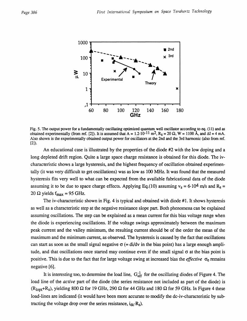
tain fundamental oscillations at frequencies within the waveguide transmission band. In Fig. 5 is the
output power as obtained from Eq. (15) compared with the experimental results for fundamental
oscillations reported in ref. [2]. In these experiments we carefully checked if any subharmonic power
could be detected in the bias circuit, as was the case for the "harmonic mode operation". Notice that
the theoretical power is obtained choosing the load resistance Rio for maximum output power i.e.
using Eq.(14)-(15). The experimental output powers are (of course) lower. By optimizing the em-
bedding impedance of the mount, reducing the series resistance of the device and the losses in the
mount, more output power should be achieved. Moreover, judging from our experiments and assum-
ing that it should be realistically possible to match the circuit to a diode with Re( Zo} = 1 0, it should
be possible to increase the diode area with a factor of 70. Hence, the output power also should im-
prove with a factor of approximately 70 (compare Fig. 5) to about 6 mW at 100 GHz.
(14)
(15)
Page 386 First International Symposium on Space Terahertz Technology
1000
100 •
2nd
x 3rd
x0
Experimental
14,A
•
Theory
,160
1
80 100 120 140 160 180G Hz
Fig. 5. The output power for a fundamentally oscillating optimized quantum well oscillator according to eq. (11) and asobtained experimentally (from ref. [2]). It is assumed that A = 1.2
. 10- 11 m2, Rs = 20 0, W = 1100 A, and AI = 4 mA.Also shown is the experimentally obtained output power for oscillators at the 2nd and the 3rd harmonic (also from ref.[2]).
An educational case is illustrated by the properties of the diode #2 with the low doping and a
long depleted drift region. Quite a large space charge resistance is obtained for this diode. The iv-
characteristic shows a large hysteresis, and the highest frequency of oscillation obtained experimen-
tally (it was very difficult to get oscillations) was as low as 100 MHz. It was found that the measured
hysteresis fits very well to what can be expected from the available fabricational data of the diode
assuming it to be due to space charge effects. Applying Eq.(10) assuming vs = 6•104 m/s and Rs =
20 1 yields fmax = 95 GHz.
The iv-characteristic shown in Fig. 4 is typical and obtained with diode #1. It shows hysteresis
as well as a characteristic step at the negative resistance slope part. Both phenomena can be explained
assuming oscillations. The step can be explained as a mean current for this bias voltage range when
the diode is experiencing oscillations. If the voltage swings approximately between the maximum
peak current and the valley minimum, the resulting current should be of the order the mean of the
maximum and the minimum current, as observed. The hysteresis is caused by the fact that oscillations
can start as soon as the small signal negative a (= di/dv in the bias point) has a large enough ampli-
tude, and that oscillations once started may continue even if the small signal a at the bias point is
positive. This is due to the fact that for large voltage swing at increased bias the effective ae remains
negative [6].
It is interesting too, to determine the load line, GI for the oscillating diodes of Figure 4. The
load line of the active part of the diode (the series resistance not included as part of the diode) is
(Riopt+Rs), yielding 800 K2 for 19 GHz, 290 K2 for 44 GHz and 180 2 for 59 GHz. In Figure 4 these
load-lines are indicated (it would have been more accurate to modify the dc-iv-characteristic by sub-
tracting the voltage drop over the series resistance, idc.Rs).
First International Symposium on Space Terahertz Technology Page 387
6. Harmonic output power.
As already mentioned the nonlinear iv-characteristic and a large oscillation voltage amplitude
will cause a large harmonic content in the resulting current waveform. Hence at "low" fundamental
oscillation frequencies, when the voltage amplitude surely is large, the oscillator ought to be very
efficient as a harmonic oscillator. Due to the symmetry of the iv-characteristic, the 3rd harmonic
should have a comparatively large amplitude. This also agrees with the result shown in Fig. 5. Be-
sides the nonlinearity of the iv-characteristic itself, another reason for a large harmonic content, is re-
laxation type oscillations (see e.g. Ref. [11]). One cannot expect a pure sinusoidal oscillation at any
frequency, not even at the highest possible frequency of oscillation. Hence, one concludes that when
output power is required at frequencies near and above fmax it is more advantageous to design the
oscillator as a harmonic oscillator. The optimum fundamental oscillating frequency is then probably tobe choosen at fosc ( 1/3).f0ut-
Also notice that the current amplitudes at the harmonic frequencies should remain large up to
frequencies well above the maximwn frequency of oscillation. Important for the performance are the
actual embedding impedances at these frequencies and the capacitance of the diode. Efficient multipli-
cation should therefore be possible to obtain to quite high output frequencies.
7. Optimizing the diode.
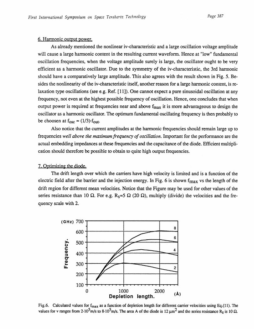
The drift length over which the carriers have high velocity is limited and is a function of theelectric field after the bather and the injection energy. In Fig. 6 is shown fmax vs the length of the
drift region for different mean velocities. Notice that the Figure may be used for other values of theseries resistance than 10 Q. For e.g. R5=5 1 (20 K2), multiply (divide) the velocities and the fre-
quency scale with 2.
(GHz) 700
600
500
a)• 400
a)a- 300
200
1000 1000 2000
Depletion length.Fig.6. Calculated values for fmax as a function of depletion length for different carrier velocities using Eq.(11). Thevalues for v ranges from 2•105m/s to 8 . 105m/s. The area A of the diode is 12 gm2 and the series resistance Rs is 10 O.
( A )
Page 388 First International Symposium on Space Terahertz Technology
For "ordinary" GaAs diodes a frequency of 600 GHz could probably be reached with a de-
pletion length of 600 A (W+lqw=700 A). However, in order to achieve this or higher frequencies, one
must understand the fundamental problems in this context. We will also show that if InAs is used in
the drift region, the higher achievable velocities will ensure a still higher fmax.
8. Optimizing the GaAs diode design.
In GaAs, electrons subjected to an electric field will travel much faster in the main r valley than
in the L valley. Since the energy of the L valley is 0.31 eV above the bottom of the r valley it can be
concluded that when carriers in an accelerating field have gained energy �0.31 eV, a transfer of the
carrier to a higher valley will occur, and the velocity of the carrier drops. Monte Carlo simulations for
GaAs [12] do show a velocity decrease when this requirement is fulfilled. Hence as a rule of thumb,
the requirement
e•Vpeak= 0.31 eV(16)
should be fulfilled in order to maintain a high mean velocity through the drift region. The peak current
voltage is the sum of the voltage over the accumulation layer in front of the QW, the voltage drop Vqw
over the QW itself and the voltage drop Yd over the drift region. From Fig. 2 and simple geometrical
arguments it is obvious that the injection energy for peak current and a symmetric double barrierstructure eVi is related to the electron excess energy eV, in the well viz. eVi =2•e . Vw (=e•Vqw) and
the accelerating field Ew in the drift region at the quantum well is
Ew=(1,+24) (17)
where Lw and Lb are the width of the well, and the width of the barriers respectively. If the potential
in the drift region is parabolic, the voltage drop over the drift region becomes Yd 0.5-Ld•Ew where
Ld is the length of the drift region. Hence with equation (17) the requirement for the mean velocity to
be as high as possible is
2V„,(2(1 2Lb) + 1) 0.31 eV,0- (18)
We propose two possible ways of decreasing Vw: i. lowering Vw by increasing the width of
the well, and ii. lowering Vw by doping the well with indium.
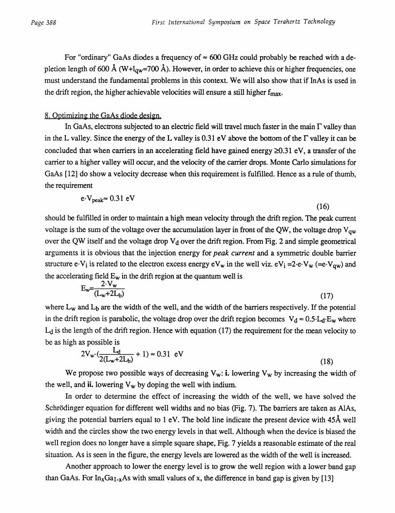
In order to determine the effect of increasing the width of the well, we have solved the
SchrOdinger equation for different well widths and no bias (Fig. 7). The barriers are taken as AlAs,
giving the potential barriers equal to 1 eV. The bold line indicate the present device with 45A well
width and the circles show the two energy levels in that well. Although when the device is biased the
well region does no longer have a simple square shape, Fig. 7 yields a reasonable estimate of the real
situation. As is seen in the figure, the energy levels are lowered as the width of the well is increased.
Another approach to lower the energy level is to grow the well region with a lower band gap
than GaA.s. For InxGai_xAs with small values of x, the difference in band gap is given by [13]

First International Symposium on Space Terahertz Technology Page 389
L E = 0.2295x2 1.1365x (19)
in eV. Roughly 85% of this difference is in the conduction band, the rest in the valence band. The
mixing of InAs with GaAs is slightly more complicated than the mixing of AlAs with GaAs since the
lattice constant of InAs is different from that of GaAs. Thus a strained layer is formed and there is a
limiting thickness to the layer that can be grown. This is discussed in [141 and it can be concluded that
for a 45 A well the maximum In content is =40%. The In-doping means that the potential barrier be-
comes higher, which should be accounted for in a more exact theoretical evaluation.
The best solution is to combine these methods and use a slightly wider well and a limited In
content in the well.
/kilts barriers, 20A.(eV) 1,0
0,8
0,6
c 0,4
0,2
0,0
11111111111101111110111111111LINI1111111111 4tiarojalrerLg
50 100 150 200 250Well width. (A)
Fig.7. The energy levels for a square well potential for well widths up to 250A. The bold line indicates the 45Awell currently used in the devices with the 6vo energy levels, one at .0.17eV and one at .0.63eV.
In the table below, is given some examples on expected fmax of different designs all with diodeareas of 12 gm2. The original experimental diode yields an fmax of approximately 170 GHz.
.Width A In % Vw meV Ew
kV/cmWopt A vs
los m/s
R. 0 fm,„ GHz Rem.
45 0 170 400 1000 1.0 20 170 Exp.diode45 0 170 400 1000 1.0 5 .23060 0 110 220
4600 1.0 5 .300
60 7 1 32 64 600 8.0 5 .60060 8 22 44 800 3.0, 5 , =50060 8 22 44 800 _ 3.0 20 200 ,
The diode we have have used in experiments was according to the upper one in the table, i.e.fmax was as low as 170 GHz. Improving the mean velocity by using In in the well and broadening the
well itself, for the same series resistance fmax will become about 200 GHz, while if Rs can be 5 CI,
one may reach fmax = 600 GHz.

(GHz) 1000
800
600
400
200
Page 390 First International Symposium on Space Terahertz Technology
It is interesting to use Eq. (15) to predict the maximum output power at e. g. 400 GHz for the
diode with 1max=600 GHz of the table above (W+1qw=700 A, v =6 1O m/s) by choosing a larger area
diode (Rs proportional to 1/A). It is reasonable to assume at that 400 GHz it is realistically possible to
match the diode to a 5 CI load resistance. This should allow us to use a 60 gm 2 area diode (Rs=1
Afr-,20 mA) yielding a maximum output power (Eq. (15)) of approximately 420 1.M. Probably only
of the order 200 11,W will be available as useful output power. Whether it is possible to achieve still
more output power at 400 GHz for a diode oscillating fundamentally at 133.3 GHz, is not clear. The
maximum output power at 133 GHz for the same diode area should be about 7 times higher, i. e. 3
mW.
9. Using InAs in the drift region.
A way to get around the problem of decreasing velocity for electrons with high energies is to
use a material combination where the lowest upper valley is higher up than the 0.31 eV in GaAs. The
upper valley in InAs is more than 1 eV higher than the r valley [13] but this is not the sole benefit of
that material system. The mobility is higher, -..:33000 cm2/Vs compared to 8500 cm2/Vs for GaAs at
room temperature [15]. Moreover, the the series resistance in this material can be made lower, partly
because the higher mobility but also since the band gap is lower it gives a lower ohmic contact resis-
tance.
0 1000 2000Depletion length. (A)
Fig. 8. Calculated values for fmax as a function of depletion length for two different series resistances 5 and 10Kasassuming vs is 106 mis and the area A of the diode is 121.110. These parameters are probably obtainable for InAs.
Experiments on this material system with quantum well diodes have been performed with good
results [16]. Large peak to valley ratios can be obtained, since barriers of AlSb in InAs are very high,
eV, compared to =1 eV for AlAs barriers in GaAs. Even though this is a new material and hardly
tested it looks to be the most promising for the future because of the possibility to get high carrier
velocity and low series resistance. The peak velocity for bulk InAs is =3.6 . 105m/s [13], around 60%
First International Symposium on Space Terahertz Technology Page 391
higher than GaAs =2.2 . 105m/s. For short distances in GaAs this peak velocity can be exceeded by
two to three times, [12]. If the same is true for InAs the maximum velocity would be approximately
10 . 105mis, and this without the necessity of having a low field outside the barriers. Due to the lower
bandgap of InAs as compared to GaAs, better ohmic contacts should be obtainable. In Fig. 8, calcu-lated values for fmax is presented with v=10 . 1C5mis and the series resistance R =10 and Rs=5
A maximum frequency is then 9OO GHz for a 5
Finally it is interesting to use Eq. (15) to predict the the maximum output power at e. g. 750
GHz for an optimized InAs diode with fmax=900 GHz (assuming Wi-lqw=1500 A, v s.10 . 105 m/s,
Rs=6 f/ for a 12 gm2 area). Assuming that at this frequency it is possible to match the diode to a load
resistance of 10 (higher losses causes a larger load resistance), the maximum power to the load (Eq.
(15))will be of the order 2501.1W. Probably only a fraction of this power (may be 50 %) will be useful
The optimum area of this diode is then about 15 gm 2, R 4.6 K2 and AI.:10 rnA. If a still lower Rs is
possible to realize, of course still higher output powers can be achieved.
10. QW-diode Multipliers.
As was pointed out in paragraph 6, the QW oscillator may be very rich in harmonics. One
should therefore expect potential high efficiency from a QW diode multiplier. We have designed a
Quantum Well (QW) diode frequency tripler with more than 1.2 % efficiency and 0.8 mW output
power at about 250 GHz [4]. A comparison between the experimental results and the theoretically cal-
culated efficiency for a tripler using such a diode has been made. The multiplier mount used in our
experiments is meant for Schottky-varactor triplers, and has a design similar to Erickson's [17]. Due
to the symmetric I-V characteristic of the QW-diode, see Figure 9, only odd harmonics are obtained
for zero bias voltage using the QW in a multiplier. This means that the current of a QW-diode pumped
by a sinusoidal signal contains mainly third and fifth harmonics. Thus the idler tuning used in this
mount at the second harmonic is of no importance in this case if the bias voltage is zero. In Figure 10
the measured efficiency versus input power for the QW-diode at three different output frequencies is
plotted. It can be seen that the efficiency increases with input power up to a certain level where it be-
comes more or less saturated. Maximum efficiency was obtained for zero voltage bias.
Using the large signal multiplier analysis program developed by Siegel et al. [18] and modified
by us for the QW-diode, the efficiency of the diode was calculated as a function of the input power. A
simple equivalent circuit consisting of a non linear capacitance in parallel with a nonlinear resistance
was assumed for the QW-diode. A series resistance represents frequency dependent (due to the "skin
effect") losses. The capacitance of the diode was assumed to vary inversely as a function of the length
L of the depletion region. The parallel resistance of the QW-diode was assumed to follow the meas-
ured I-V characteristic of the diode, see Figure 9. The frequency dependent series resistance of the
QW-diode was calculated to be between 22-32 (at 83 GHz) depending on the contact resistance
(measured to be between 2-10- 6 - 440'6 Ocm2) of the chip.

n• GaAs substrate
10000 GaAs >10i8c.44202000 A GaAs 2 x 10¹⁷crt:C50 A GaAs urxioped20A uncoped 1 5
45 A GaAs a-looped20A AtAs undoped 1050 A GaAs unooped
2000 A GaAs 2x10¹⁷crri3
4000 GaAs > 10 18crn3 5
-1. -3 -2 -1
-5
-10
-15
a
Page 392 First International Symposium on Space Terahertz Technology
Fig. 9. The IV-characteristic of the QW-diode used in the multiplier experiments.
1,0
0,5
2,5
2,0
1,5
0,0 1 I . I I I I
0 10 20 30 40 50mW
Fig. 10. Measured and calculated efficiency vs input power for the tripler.(a): measured efficiency at 242 GHz.(s): measured efficiency at 249 GHz.(E): measured efficiency at 257 GHz.(A): calculated efficiency for 249 GHz, contact resistance is 2.107 6 D.cm2.(L): calculated efficiency for 249 GHz, contact resistance is 4.10- 6 fkm2.
60 70
First International Symposium on Space Terahertz Technology Page 393
The theoretically calculated results at an output frequency of 249 GHz are shown in Figure 10
for -0.2V bias voltage zero bias). It is seen that one for a contact resistance of 4 . 10-6 Ocm2 the
experimental and theoretical curves agree. However, due to the negative differential resistance above
about 2V (see Figure 9) the program did not always converge, as indicated by the broken line curve in
Figure 10.
At the points "A" in Figure 10 the theoretically calculated efficiency starts to increase. This is
due to the voltage swing of the pump signal across the QW-diode exceeds the voltage for peak current
in the I-V characteristic of the diode, see Figure 9. Thus the negative differential resistance portion of
the I-V characteristic of the QW enhances the efficiency of the tripler.
It can be seen that the general behaviour of the theoretical curves agree well with the measured
ones. Thus the simple equivalent circuit applied here for the QW-diode could be used as a first
approximation for the diode. The equivalent circuit of the QW-multiplier is further investigated in Ref.
[1
11. OBV-diode multipliem
A new device, the Quantum-Barrier-Varactor diode (QBV-diode), has been proposed by us for
use in multipliers for millimeter-waves [20]. Since the capacitance vs voltage characteristic is sym-
metric, only odd harmonics are obtained. Hence there is no idler circuit to consider for the tripler and
only one for the quintupler. It is shown that for triplers and quintuplers, the theoretical efficiency
using QBV's is comparable or possibly larger than using Schottky-varactor diodes.
By making the width and/or the height of the barrier in the QBV-diode such that the conduction
current through the device is negligible for the voltage interval defined by the pump voltage swing,
the device can be modelled simply as a voltage dependent capacitance.
A QBV-diode may be fabricated in the same way as the quantum well mesa diode, but with the
epitaxial GaAs/AlGaAs/GaAs material designed as indicated in Fig. 11. The AlGaAs bather will to a
large extent prevent electrons to pass through the structure and will cause a depleted region with a
voltage dependent width, which is associated with a voltage dependent capacitance C(V). When the
diode is biased in the forward direction, the depleted region will appear on one side of the barrier, and
the depletion capacitance of the device will decrease with increasing voltage. Since the diode is essen-
tially symmetric, a reversed bias will in the same way cause a decrease of the capacitance of the de-
vice. Hence, the maximum capacitance is obtained for zero voltage and is determined by the thickness
of the AlGaAs barrier. The minimum capacitance, which occurs for maximum bias voltage, is deter-
mined by the doping concentration and the extension of the low doped region "L" (see Fig. 11). In
fact a similar capacitance swing vs voltage as for the Schottky-varactor diode is expected. It is ob-
vious that in future work one should search for optimum doping profiles.

n*GaAs substrate10000 A GaAs, 5)(10'8
rri-3
50 A GaAs undoped2004 A10 7 Ga 0 3As
• undoped50 A GaAs, undoped
400 0 A GaAs, z5x10
18 ern-3
TeSCIcontac
avalanchebreakdowrt
Page 394 First International Symposium on Space Terahertz Technology
100
-60 -40 -20 0V
avalanchebreakdown
20 40 60
30
2 0
1 0
<0
-10
-20
-30
- 80
- 60 u_
40
20
Fig.11 The doping profile of the mesa structure. Also shown is the 1-V and C-V characteristic of the diode with 0.4•5pm, L.4000 A, and Nd=2•1017 cm2, assuming no avalanche breakdown. The avalanche breakdown will limit the allow-able if-voltage swing.
For the QBV-diode as well as for the Schottky-varactor diode, the series resistance R s(V) is
bias dependent. In order not to overestimate the QBV-diode multiplier efficiency, we have in the cal-
culations presented below, used a constant depletion region series resistance contribution equal toRdepunax. Notice that for a Schottky-varactor diode tripler, the idler current at 2-co p will deteriorate
the tripler performance, since any finite reactance termination will cause power losses in the series re-
sistance.
An I-V profile for a quantum barrier alone, consisting of AloaGa0 .3As with a length of 200 A,
has been determined from experiments [21]. Using this information, we calculated the I-V and C-V
characteristics for a 4.5 gm device with this barrier followed by a 4000 A low doped region
(ND=2-10 17 cm-3) (see Fig. IA). Notice (Fig. 11) that the differential conductance defined as MAW
is quite small compared to (0C.
Using a large signal multiplier analysis program based on the principle of harmonic balance de-
veloped by Siegel et. al. [18] and modified by us for the QBV-diode, the efficiency of the QBV-mul-
tiplier was calculated for a few different device structures as a function of input power. The equivalent
circuit of the device and the procedure for optimization are very similar to those used for the Quantum
Well multiplier in ref. [4].
The theoretical efficiency vs input power for a tripler to 105 GHz is shown in Fig. 12. The
length of the region "L" is chosen to be 4000 A and the doping of the region is used as the parameterin Fig. 12. As mentioned above the series resistance used in these calculations is R s = Rdepl.max
Rcontact, where
R.contact is assumed equal to 3.14 K2 corresponding to a contact resistance of 0.5x10⁻⁶
ohm cm2. The results presented in Fig. 12 show that the conversion efficiency is high for low input
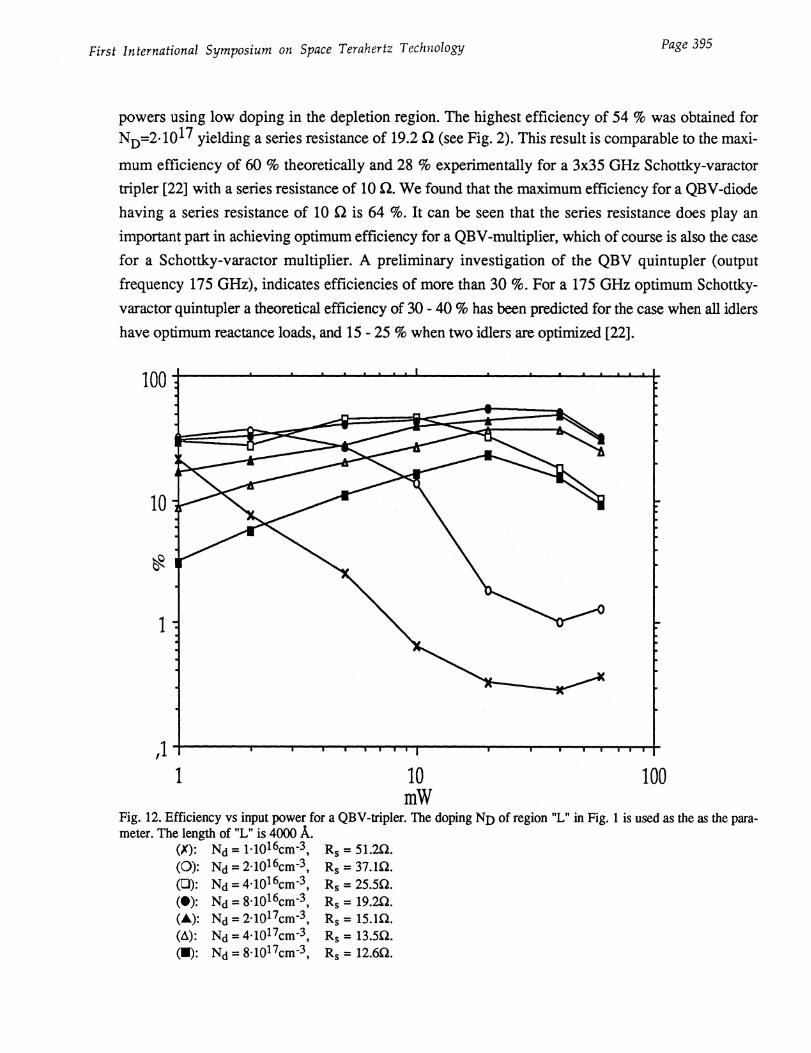
First International Symposium on Space Terahertz Technology Page 395
powers using low doping in the depletion region. The highest efficiency of 54 % was obtained forND=2 . 10 17 yielding a series resistance of 19.2 (see Fig. 2). This result is comparable to the maxi-
mum efficiency of 60 % theoretically and 28 % experimentally for a 3x35 GHz Schottky-varactor
tripler [22] with a series resistance of 10 CI. We found that the maximum efficiency for a QBV-diode
having a series resistance of 10 II is 64 %. It can be seen that the series resistance does play an
important part in achieving optimum efficiency for a QBV-multiplier, which of course is also the case
for a Schottky-varactor multiplier. A preliminary investigation of the QBV quintupler (output
frequency 175 GHz), indicates efficiencies of more than 30 %. For a 175 GHz optimum Schottky-
varactor quintupler a theoretical efficiency of 30 - 40 % has been predicted for the case when all idlers
have optimum reactance loads, and 15 - 25 % when two idlers are optimized [22].
100
11 I
1 10 100mW
Fig. 12. Efficiency vs input power for a QBV-tripler. The doping ND of region "L" in Fig. 1 is used as the as the para-meter. The length of "L" is 4000 A.
00: Nd = 1-10 16cm-3 , Rs = 51.2.Q.(0): Nd = 21016cm-3 , Rs = 37.10.
Nd = 4 . 1016cm-3 , Rs = 25.50.(•). Nd = 8 . 1016cm-3 , Rs = 19.2.Q.(A): Nd = 2 . 1017cm-3 , Rs = 15.10.(A): Nd = 4°10 17cm-3 , Rs = 13.50.(II): Nd = 81017cm-3 , Rs = 12.6a.

Page 396 First International Symposium on Space Terahertz Technology
It is essential also that the ohmic contact is reasonably good, although at the high frequencies
involved even a contact with poor de-qualities will work well [23]. The optimum doping profile may
actually be different for different frequencies of operation. The reason is that the doping profile has
an influence on not only C(V), but also on the I-V characteristic, i. e. the conductance G(V)=d1kIV,
which is in parallel with C(V). As a rule of thumb, G ought to be small as compared to the minimumparallel susceptance toC for the whole bias voltage range.
We here fabricated a first batch of 0 = 3 jtm QBV-diodes using MBE-material (from IMEC in
Leuven, Belgium). The barrier consist of 210 A AlGaAs with 70% Al. Outside the barrier a 50 A un-
doped spacer layer of GaAs is grown. Outside these spacer layers on each side 5300 A region ofGaAs is grown, doped to 1-10 17 cm-3 followed by highly doped GaAs to provide good ohmic con-
tacts. The initially measured IV-characteristics showed a current density about 810 5 times larger than
expected. We intend to address this problem in the near future.
Despite the too large current density, the conversion efficiency was reasonably high. The
experiments were conducted in a Schottky-varactor waveguide tripler structure of the same design as
described in Ref.[17]. For an output frequency of 225 GHz a maximum efficiency of more than 5 %
and an output power of more than 2 mW was measured. For a good Schottky-varactor diode tripler
for the same frequency, using diodes from Univ. of Virginia (type 6P2), an efficiency of about 4.5 %
was obtained. A theoretical analysis of the efficiency of the used diodes yielded ri 6.4 %, while a
diode with the expected smaller current should offer Ti 13.6 % efficiency for 32 mW input power.
An ohmic contact resistance for the mesas of 3-10- 6 ohm cm2 was assumed in the analyze [4].
12. Conclusions.
The work on applications of QW-diodes for millimeter waves and submillimeter waves have
only started. Although the oscillator power obtained experimentally so far is low, it is sufficient in
some applications such as for local oscillators in superconducting mixers or as a signal source for
measurement systems. The main design problems are related to the device itself and the minisubmm-
wave circuit, which should yield the optimum embedding impedance(s) required by the device. Be-
sides oscillators and multipliers, mixers with gain can be constructed. However, it is not yet known
whether it will be possible to achieve low mixer noise.
The QBV-diode is potentially a very competitive device in millimeter-wave multiplier applica-
tions. The obtainable multiplier efficiency with a QBV-diode is shown to be comparable to corre-
sponding Schottky-varactor multipliers. The main advantage is that idler tuning is not required for a
tripler, and only one (two) idler(-s) has to be considered for a quintupler (heptupler).
First International Symposium on Space Terahertz Technology Page 397
13. Acknowledgements.
The author would like to thank Dr. T. Andersson and Mr. J. SOderstriim for their kind supply
of MBE-material for the experimental quantum well diodes and Prof. S. Yngvesson for useful dis-
cussions. Milena Mattas is acknowledged for her help in drawing most of the figures. The Swedish
board for Technical Development and the European Space Agency (ESTEC contract RFQ/3-
6172/88/NL/PB) are acknowledged for financial support.
References.
[1] T. C. L. G. Soliner, E. R. Brown, W. D. Goodhue and H. Q. Le, "Observations of millimeter-wave oscillations from resonant tunneling diodes and some theoretical considerations of ultimatefrequency limits," Appl. Phys. Lett., vol. 50, pp. 332 - 334, 1987.
[2] A. Rydberg, H. GrOnqvist, E. Kollberg, "A theoretical and experimental investigation on milli-meter-wave quantum well oscillators, Microwave and Optical Technology letters, vol. 1, pp.333 - 336, 1988.
[3] L. L. Chang, L. Esaid, R. Tsu, "Resonant Tunneling in Semiconductor Double Barriers," Appl.Phys. Lett., vol. 24, pp. 593 - 595, 1974.
[4] A. Rydberg and H. Griinqvist, "Quantum well high efficiency millimeter-wave frequencytripler," El. Lett. vol. 25, pp. 348 - 349, 1989.
[5] A. Mortatzawi, V. P. Kesan, D. P. Neikirk, and T. Itoh, "A self oscillating QWITT diodemixer", to be published in the Proceedings of the 19th European Microwave Conference, Lon-don, 1989.
[6] E. Kollberg, "Superconducting Devices and Quantum Well Diodes in Low Noise HeterodyneReceivers, Part 2: Quantum Well Diodes", Alta Frequenza, Vol. LVIII, No 5-6, pp. 521-530,1989.
[7] V. P. Kesan, D. P. Neikirk, P. A. Blakey, B. G. Streetman and T. D. Linton, "The influenceof transit-time effects on the optimum design and maximum oscillation frequency of quantumwell oscillators," IEEE Trans. on Electron Devices, vol. ED-35, pp. 405 - 413, 1988.
[8] E. R. Carlson, M. V. Schneider and T. F. McMaster, "Subharrnonically pumped millimeter-wave mixers," IEEE Trans. Microwave Theory and Techniques, vol. MTT-26, pp. 706 -715,1978.
[9] E. R. Brown, W. D. Goodhue and T. C. L. G. Soliner, "Fundamental oscillations up to 200GHz in resonant tunneling diodes and new estimates of their maximum oscillation frequencyfrom stationary-state tunnel theory," J. Appl. Phys., vol. 64, pp. 1519 - 1529, 1988.
[10] H. GrOnqvist, A. Rydberg, H. Hjelmgren, H. Zirath, E. Kol'berg, J. SOderstrOm, and T.Andersson, "A millimeter wave quantum well diode oscillator," Proceedings 18th EuropeanMicrowave Conference, Stockholm, pp. 370-375, 1988.
[11] M. A. Lee, B. Easter, and H. A. Bell, Tunnel diodes, Chapman and Hall, London, 1967.
[12] LY-F. Tang and K. Hess, "Investigation of Transient Electronic Transport in GaAs FollowingHigh Energy Injection.", IEEE Trans. Electron Devices, VoLED-29, pp.1906-1911, 1982.
Page 398 First Internatic;zal Symposium on Space Terahertz Technology
[13] "Landolt-Biimstein, Numerical Data and Functional Relationships in Science and Technol-ogy.", Vol.17a, Springer-Verlag Berlin, 1982.
[14] T.G. Andersson, Z.G. Chen, V.D. Kulakovskii, A. Uddin, J.T. Vallin, "Variation of the Criti-cal Layer Thickness with In Content in Strained InxGal-xAs-GaAs Quantum Wells Grown byMolecular Beam Epitaxy.", Appl. Phys. Lett. Vol.51, pp.752-'754, 1987.
[15] S.M. Sze, "Physics of Semiconductor Devices.", Wiley, 1981.
[16] J.R. SOderstrOm, D.H. Chow, T.C. McGill, "InAs/AlSb Double Barrier Structure with LargePeak-to-Valley Ratio: A Candidate for High Frequency Microwave Devices.", To be published.
[17] N.R. Erickson, "A high frequency tripler for 230 GHz," Proc. European Microwave Conf.1982, pp. 288-292.
[18] P.H. Siegel, A.R. Kerr and W. Hwang, "Topics in the Optimization of Millimeter WaveMixers," Nasa Technical Paper 2287, March 1984.
[19} A. Rydberg, "On the Design of Quantum-Well Multipliers", Proc. 14th International Confer-ence on Infrared and Millimeter Waves, Wiirzburg, BRD, pp. 467-468, 1989.
[20] E. Kollberg and A. Rydberg, "Quantum-Barrier-Varactor Diodes for High Efficiency Milli-meter-Wave Multipliers.", Electronics Letters, Vol. 25, No. 25, pp. 1696-1697, 1989.
[21] I. Hase, H. Kawai, K. Kaneko and N. Watanabe, "Electron transport through the MOCVDgrown GaAs/A1GaAs/GaAs heterojunction barrier," Electronics Lett., vol. 20, pp. 491-492,1984.
[22] T.J. Tolmunen, "High efficiency Schottky-varactor frequency multipliers at millimeter waves,"Thesis for doctor of Technology degree, Helsinki University of Technology, Report S 180,1989. (Partly published in Int. J. of Infrared and Millimeter Waves, vol. 8, pp. 1313 - 1353(1987) and vol 9, pp. 475 - 518 (1989))
[23] H. Zirath, "On the high-frequency behaviour of ohmic contacts," Proc. 19'th European SolidState Device Research Conference ESSDERC89, Berlin, BRD, pp. 63-66, 1989.