Quilt Packaging® For Power Electronics - PSMA...Quilt Packaging (QP) Technology •Edge-connections...
35
Quilt Packaging® For Power Electronics Jason M. Kulick President, Co-Founder Indiana Integrated Circuits, LLC 21 March 2013
Transcript of Quilt Packaging® For Power Electronics - PSMA...Quilt Packaging (QP) Technology •Edge-connections...

Quilt Packaging® For Power Electronics
Jason M. Kulick
President, Co-Founder
Indiana Integrated Circuits, LLC
21 March 2013

Overview
• Introduction
• Quilt Packaging (QP) technology
– Concept
– Examples
– Advantages
– QP progress in power
2
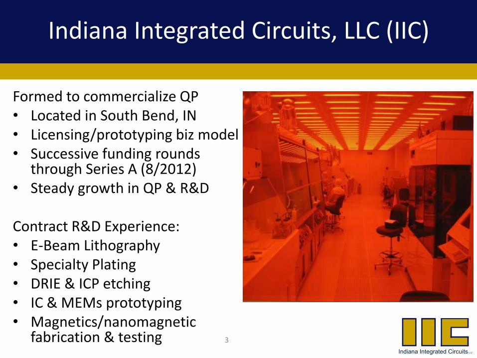
Indiana Integrated Circuits, LLC (IIC)
Formed to commercialize QP • Located in South Bend, IN • Licensing/prototyping biz model • Successive funding rounds
through Series A (8/2012) • Steady growth in QP & R&D Contract R&D Experience: • E-Beam Lithography • Specialty Plating • DRIE & ICP etching • IC & MEMs prototyping • Magnetics/nanomagnetic
fabrication & testing 3

Quilt Packaging (QP) Technology
• Edge-connections joined to create multi-chip “quilt,” developed at Notre Dame
• “Monolithic” assemblies from same or disparate materials & process technologies
• Extremely low impedances
• Enables optimization for cost and functionality
• Industry-standard tools and fabrication processes
4
CHIP 1 CHIP 2

QP-Interconnect Structures
• Edge connection structures called “nodules”
• Solid metal, typically 10-200 um wide, ~ 20-50 um thick
• Customizable shapes-including interlocking-enables sub-micron chip alignment
5

QP Customizable I/O
6

Sub-Micron Chip Alignment
7
= 30 micron
Interior (left) of four-chip quilt (above) QP enable extremely accurate alignment

Si QP 2x2 Array (1 in^2 chips)
8

~15 um gap post-solder
9

Inner seam of 4-chip Si test quilt
10
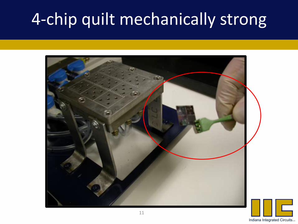
4-chip quilt mechanically strong
11
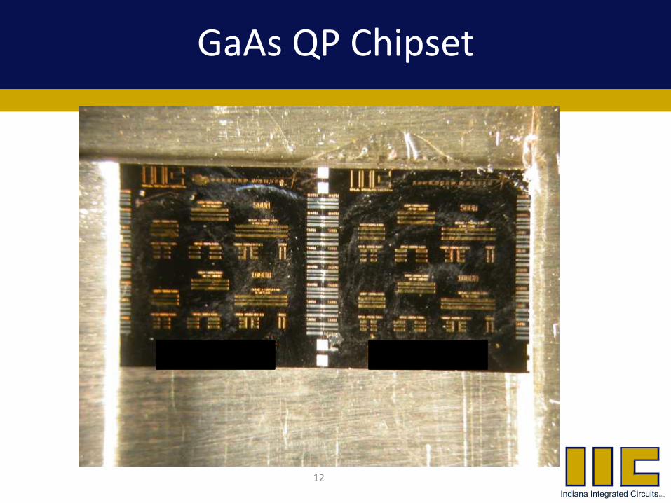
GaAs QP Chipset
12

GaAs Measurement Data Sample
Raw S-parameters De-embedded S-parameters
*Less than 3 dB insertion loss at 220 GHz

QP Microwave Performance
Less than 0.1 dB insertion loss from 50 MHz past 100 GHz, with no resonances. Recent unpublished results under 0.9 dB at 180 GHz
14

QP Eye diagrams
• Measurement of 12 Gb/s eye pattern (Anritsu MP1763B)
– Horiz. 100 mV/div
– Vert. 20 ps/div
• Data stream: 231-1 pseudo-random bit sequence
• Nearly ideal interconnect performance; indistinguishable from PG.
• Error-free operation
– SNR (Q) = 12.9 for pattern generator alone, 12.4 after chip-to-chip interconnect
Raw pattern generator
50 µm GSG eye
15

QP Time-Domain Performance
• Single-ended GSG CPW configuration
• Picosecond Pulse Labs 4022 TDR pulse enhancement module: < 9 ps risetime
• Total delay including probe pads, launcher: 7 ps (820 μm length)
• Delay due to QP nodules: 2.7 ps
100 µm nodule compared with
pads/launcher, GSG
16

“3D-QP” and “Interposers”
• QP can enable multiple 3D configurations
• 3D-QP retains many advantages of 2D-QP
• “Quilting” interposers can decrease form-factor
• Systems benefit from QP without having to redesign chips
17

3D Si QP Test Articles
18

Advantages of Quilt Packaging
• Optimized integration of disparate materials and process technologies (Si, GaN, GaAs, AlN, more)
• Chip partitioning for optimal yield/functionality
• Increased cross-sectional area vs. WBs, bumps
• Better thermal management & failure modes compared to WB
• Reduced design time due to applicability of current 2-D tools, design re-use
• IP flexibility, security
19

Original intent-test using wirebonds
20

Early test articles--couldn’t wirebond, had to probe directly
21

Joule heating simulation through nodules interconnect (setup)
22
Silicon
Copper
Sn Solder
DC SourceElectrode
GroundElectrode

Joule heating simulation through quilted interconnect (no showstoppers)
23

Simulations don’t include heatsink, nodule size 30 um X 20 um
24
0
50
100
150
200
250
0 1 2 3 4 5 6 7 8
Current (A)
Tem
per
atu
re (C
)
Temperature Across Quilted Nodule (30um x 25 um cross area) w/ Metal 1 From Applied Current

Si QP Max current probe test (before), nodule size 30 um X 20 um
25

Si QP Max current test--probes fail before nodules (~2.25A)
26
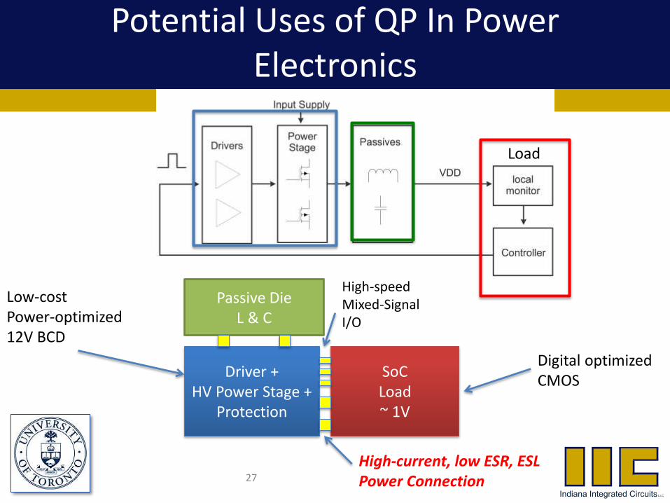
Potential Uses of QP In Power Electronics
27
Driver +
HV Power Stage + Protection
SoC Load ~ 1V
High-speed Mixed-Signal I/O
High-current, low ESR, ESL Power Connection
Low-cost Power-optimized 12V BCD
Passive Die
L & C
Load
Digital optimized CMOS

Potential Uses of QP In Power Electronics
28
HV GaN/GAs Power Stage
SoC Load ~ 1V
High-speed Mixed-Signal I/O
High-current, low ESR, ESL Power Connection
Low-cost CMOS or BCD
Passive Die
L & C
Load
Optimized High-
Speed Driver + Protection
Digital optimized CMOS

Potential Uses of QP In Power Electronics
29
Driver +
HV Power Stage + Passives on Silicon
SoC Load ~1V
High-speed Mixed-Signal I/O
BCD or GaN/GAs with On-chip drivers
Load
Digital optimized CMOS
High-current, low ESR, ESL Power Connection

Future Work
• Thermal cycle/shock testing of preliminary “quilts” (ongoing)
• Completion of DC-DC converter demonstration (3-chip quilt w/QP Si interposer---ongoing)
• GaN QP (just starting)
• Chip architectures & partitioning for power
• Other?---Specific partner applications, etc.
30

Thank You!
For More Information Contact:
Jason Kulick
(574) 217-4612
And/or visit:
www.indianaic.com
31
QP Fabrication Process Flow Overview
• Very similar to “via-middle” TSV process
• Utilizes industry-standard tools & processes
• At least 2 additional mask steps
– Nodule definition
– Separation
• Most unique feature is dry etch step for singulation
• After assembly, handle as if “normal” chip
32

QP Fabrication-Nodule Definition
33

QP Fabrication- Nodule Metallization
34

QP Fabrication-Die Singulation
35


![Third-line treatment and 177Lu-PSMA radioligand therapy of ... · refractory adenocarcinomas of the prostate express prostate-specific membrane antigen (PSMA) [13]. 68Ga-PSMA HBED-CC](https://static.fdocuments.in/doc/165x107/5f0256ec7e708231d403c8b9/third-line-treatment-and-177lu-psma-radioligand-therapy-of-refractory-adenocarcinomas.jpg)