Quick Troubleshooting Manual for Mitsubishi WS-55859
25
MITSUBISHI DIGITAL ELECTRONICS V19 / V 21 PWB Level Troubleshooting Guide
-
Upload
john-smith -
Category
Documents
-
view
41 -
download
3
Transcript of Quick Troubleshooting Manual for Mitsubishi WS-55859
MITSUBISHI DIGITAL ELECTRONICSV19 / V21
PWB Level Troubleshooting Guide
iiii
V19 / V21
PWB Level Troubleshooting Guide
©2002 Mitsubishi Digital Electronics9351 Jeronimo Rd.Irvine, CA 92618
All Rights Reserved
V19 / V21 PWB Level Troubleshooting Guide
iiiiiiii
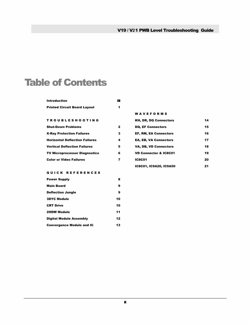
Table of ContentsIntroduction iiiiiiiiiiii
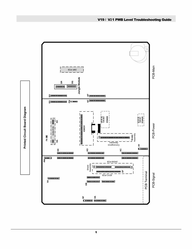
Printed Circuit Board Layout 1
T R O U B L E S H O O T I N G
Shut-Down Problems 2
X-Ray Protection Failures 3
Horizontal Deflection Failures 4
Vertical Deflection Failures 5
TV Microprocessor Diagnostics 6
Color or Video Failures 7
Q U I C K R E F E R E N C E S
Power Supply 8
Main Board 9
Deflection Jungle 9
3DYC Module 10
CRT Drive 10
2HDW Module 11
Digital Module Assembly 12
Convergence Module and IC 13
W A V E F O R M S
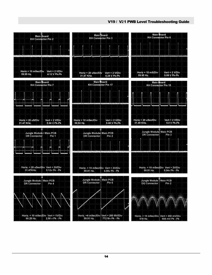
KH, DR, DQ Connectors 14
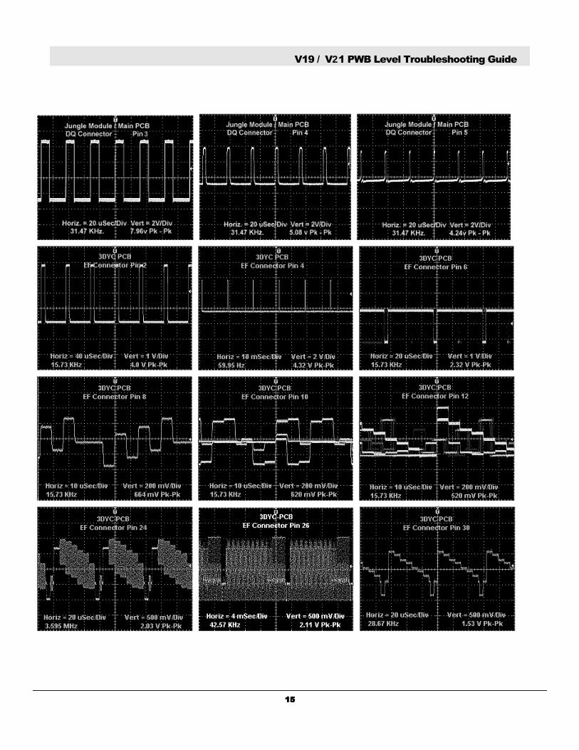
DQ, EF Connectors 15
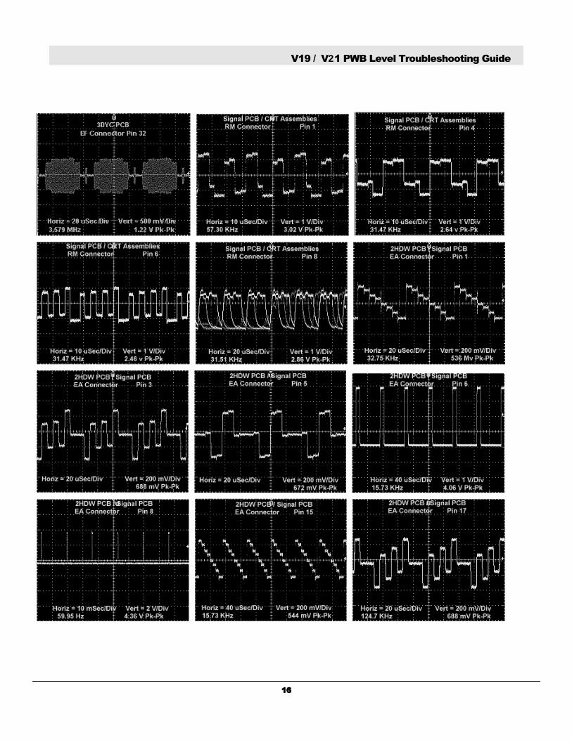
EF, RM, EA Connectors 16
EA, EB, VA Connectors 17
VA, DB, VD Connectors 18
VD Connector & IC8C01 19
IC8C01 20
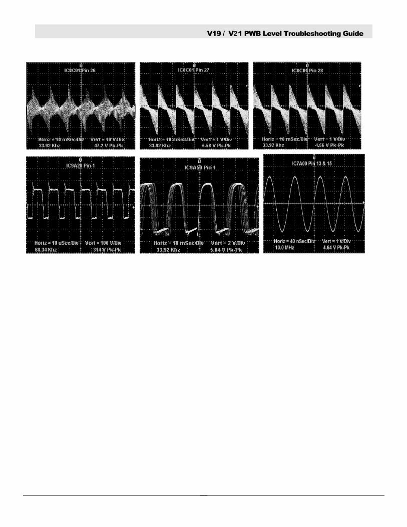
IC8C01, IC9A20, IC9A50 21
V19 / V21 PWB Level Troubleshooting Guide
iiiiiiiiiiii
Introduction
The purpose of this V19 / V21 PWB Level Troubleshooting Guide is to assist the servicer to quickly identify commonchassis test points, and to facilitate efficient servicing procedures in the field or service shop / depot. It is intended for usein tandem with the Service manual as an aid to troubleshooting a set. Included are many major DC voltage measurementsand AC waveforms pertinent to proper operations of the chassis. In addition, troubleshooting procedures are provided forsome common service issues a Technician may encounter.
This guide is not intended to be used as a resource for technical training, circuit analysis, or adjustment procedures. Referto the V19 / V21 Technical Training guide and/or the Service manual which includes all schematics, parts lists, andadjustment procedures for these purposes.
V19 / V21 PWB Level Troubleshooting Guide
1111
Pri
nte
d C
ircu
it B
oar
d D
iag
ram
PC
B-S
igna
lP
CB
-Pow
erP
CB
-Mai
n
Jun
gle
Mo
du
le
DR
DQ
KH
KH
Shi
eld
Ass
embl
y
3DYC-PCB
2HDW-PCB
EB
EA
RM
KE
KD
KC
EF
PF
DA
RF
VA
DB
Shi
eld
Ass
embl
y
ConvergenceGenerator
VD
KF
KF
Hea
tsin
k A
ssy
IC8C
01
DBF-PCB
PM
SV
M-P
CB
FA
KK
KA
IC9A
20
IC9A
50
PC
B T
erm
inal
V19 / V21 PWB Level Troubleshooting Guide
2222
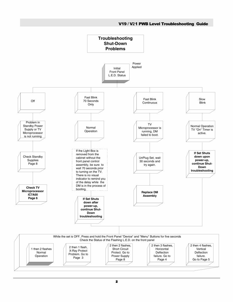
InitialFront Panel
L.E.D. Status
PowerApplied
OffFast Blink
70 SecondsOnly
Fast BlinkContinuous
Slow Blink
Problem inStandby PowerSupply or TV
Microprocessoris not running
Check StandbySuppliesPage 8
Check TVMicroprocessor
IC7A00Page 6
NormalOperation
If the Light Box isremoved from thecabinet without thefront panel controlassembly, be sure towait 70 seconds priorto turning on the TV.There is no visualindicator to remind youof the delay while theDM is in the process ofbooting.
TVMicroprocessor is
running, DMfailed to boot.
UnPlug Set, wait30 seconds and
try again.
Replace DMAssembly
Normal OperationTV "On" Timer is
active.
If Set Shutsdown afterpower-up,
continue Shut-Down
troubleshooting
If Set Shutsdown uponpower-up,
continue Shut-Down
troubleshooting
While the set is OFF, Press and hold the Front Panel "Device" and "Menu" Buttons for five secondsCheck the Status of the Flashing L.E.D. on the front panel
2 then 1 flash,X-Ray ProtectProblem. Go to
Page 3
2 then 4 flashes,Vertical
Deflectionfailure.
Go to Page 5
2 then 2 flashes,Short Circuit
Protect. Go toPower Supply
Page 8
2 then 3 flashes,HorizontalDeflection
failure. Go toPage 4
TroubleshootingShut-DownProblems
1 then 2 flashesNormal
Operation
V19 / V21 PWB Level Troubleshooting Guide
3333
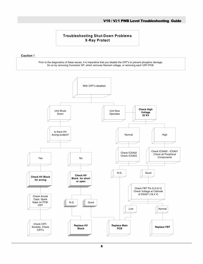
With CRT's disabled
Unit ShutsDown
Unit NowOperates
Is there HVArcing evident?
NoYes
Check AnodeCaps, Spark
Gaps on PCB-CRT
Check CRT-Sockets. Check
CRT's
Check HighVoltage32 KV
Normal High
Check IC5A02Check IC5A03
Replace MainPCB
Check FBT Pin 8 (2.8 V)Check Voltage at Cathode
of D5A57 (18.4 V)
Replace FBT
N.G.
Check IC5A00 - IC5A01Check all Peripheral
Components
Low Normal
Good
Prior to the diagnostics of these issues, it is imperative that you disable the CRT's to prevent phosphor damage.Do so by removing Connector SP, which removes filament voltage, or removing each CRT-PCB.
Troubleshooting Shut-Down ProblemsX-Ray Protect
Caution !
Check HV Blockfor arcing
Check HVBlock for short
or open
Replace HVBlock
N.G. Good
V19 / V21 PWB Level Troubleshooting Guide
4444
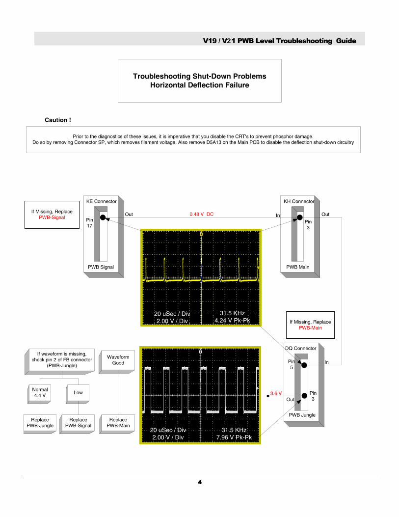
PWB Signal
KE Connector
Pin17
PWB Main
KH Connector
Pin3
20 uSec / Div2.00 V / Div
31.5 KHz4.24 V Pk-Pk
0.48 V DCIf Missing, ReplacePWB-Signal
PWB Jungle
DQ Connector
Pin5
If Missing, ReplacePWB-Main
Pin3
Out Out
Out
In
In
20 uSec / Div2.00 V / Div
31.5 KHz7.96 V Pk-Pk
3.6 V
Prior to the diagnostics of these issues, it is imperative that you disable the CRT's to prevent phosphor damage.Do so by removing Connector SP, which removes filament voltage. Also remove D5A13 on the Main PCB to disable the deflection shut-down circuitry
Troubleshooting Shut-Down ProblemsHorizontal Deflection Failure
Caution !
If waveform is missing,check pin 2 of FB connector
(PWB-Jungle)
Normal4.4 V
Low
ReplacePWB-Jungle
ReplacePWB-Signal
WaveformGood
ReplacePWB-Main
V19 / V21 PWB Level Troubleshooting Guide
5555
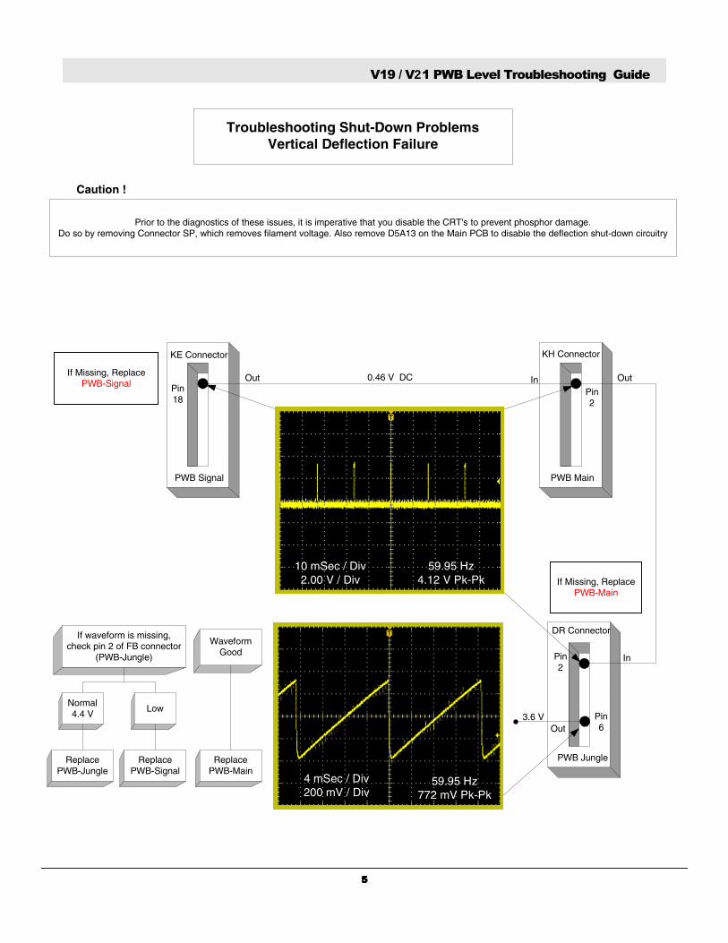
PWB Signal
KE Connector
Pin18
PWB Main
KH Connector
Pin2
20 uSec / Div2.00 V / Div
31.5 KHz4.24 V Pk-Pk
0.46 V DCIf Missing, ReplacePWB-Signal
PWB Jungle
DR Connector
Pin2
If Missing, ReplacePWB-Main
Pin6
Out Out
Out
In
In
20 uSec / Div2.00 V / Div
31.5 KHz7.96 V Pk-Pk
3.6 V
10 mSec / Div2.00 V / Div
59.95 Hz4.12 V Pk-Pk
4 mSec / Div200 mV / Div
59.95 Hz772 mV Pk-Pk
Troubleshooting Shut-Down ProblemsVertical Deflection Failure
Prior to the diagnostics of these issues, it is imperative that you disable the CRT's to prevent phosphor damage.Do so by removing Connector SP, which removes filament voltage. Also remove D5A13 on the Main PCB to disable the deflection shut-down circuitry
Caution !
If waveform is missing,check pin 2 of FB connector
(PWB-Jungle)
Normal4.4 V
Low
ReplacePWB-Jungle
ReplacePWB-Signal
WaveformGood
ReplacePWB-Main
V19 / V21 PWB Level Troubleshooting Guide
6666
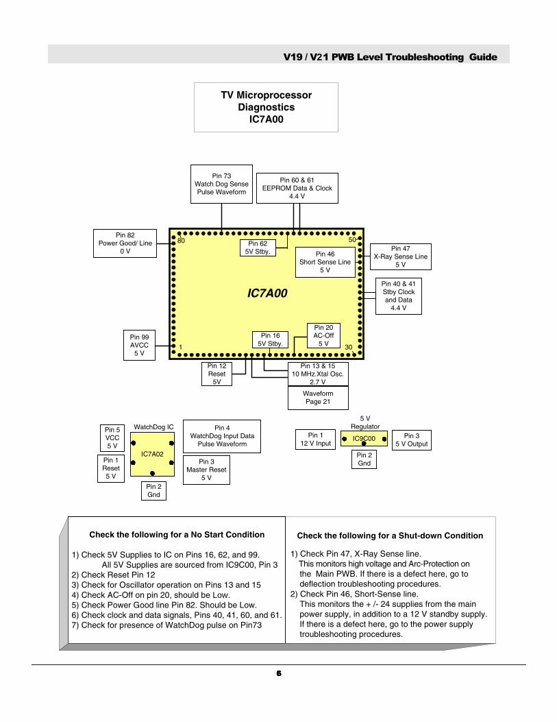
IC7A00
1 30
5080
Pin 12Reset
5V
Pin 13 & 1510 MHz.Xtal Osc.
2.7 V
Pin 165V Stby.
Pin 20AC-Off
5 V
Pin 40 & 41Stby Clockand Data
4.4 V
Pin 46Short Sense Line
5 V
Pin 47X-Ray Sense Line
5 V
Pin 625V Stby.
Pin 73Watch Dog SensePulse Waveform
Pin 60 & 61EEPROM Data & Clock
4.4 V
Pin 82Power Good/ Line
0 V
Pin 99AVCC
5 V
IC7A02
WatchDog IC
Pin 1Reset5 V
Pin 3Master Reset
5 V
Pin 4WatchDog Input Data
Pulse Waveform
Pin 5VCC5 V
Pin 2Gnd
IC9C00
5 VRegulator
Pin 112 V Input
Pin 35 V Output
Pin 2Gnd
Check the following for a No Start Condition
1) Check 5V Supplies to IC on Pins 16, 62, and 99.All 5V Supplies are sourced from IC9C00, Pin 3
2) Check Reset Pin 123) Check for Oscillator operation on Pins 13 and 154) Check AC-Off on pin 20, should be Low.5) Check Power Good line Pin 82. Should be Low.6) Check clock and data signals, Pins 40, 41, 60, and 61.7) Check for presence of WatchDog pulse on Pin73
Check the following for a Shut-down Condition
1) Check Pin 47, X-Ray Sense line. This monitors high voltage and Arc-Protection on the Main PWB. If there is a defect here, go to deflection troubleshooting procedures. 2) Check Pin 46, Short-Sense line. This monitors the + /- 24 supplies from the main power supply, in addition to a 12 V standby supply. If there is a defect here, go to the power supply troubleshooting procedures.
TV MicroprocessorDiagnostics
IC7A00
WaveformPage 21
V19 / V21 PWB Level Troubleshooting Guide
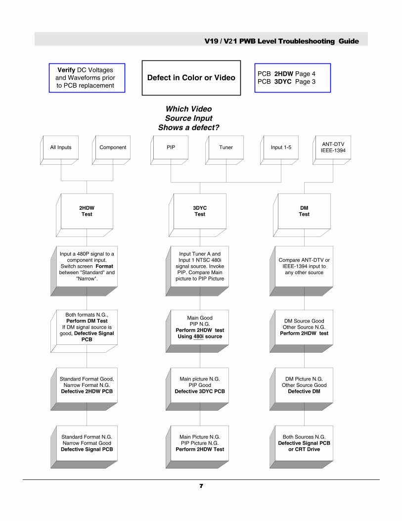
7777
Standard Format N.G.Narrow Format Good
Defective Signal PCB
Input a 480P signal to acomponent input.
Switch screen Formatbetween "Standard" and
"Narrow".
All Inputs
Which VideoSource Input
Shows a defect?
Component PIP Tuner Input 1-5ANT-DTVIEEE-1394
3DYCTest
DMTest
2HDWTest
Both formats N.G.,Perform DM Test
If DM signal source isgood, Defective Signal
PCB
Standard Format Good,Narrow Format N.G.
Defective 2HDW PCB
Input Tuner A andInput 1 NTSC 480i
signal source. InvokePIP. Compare Main
picture to PIP Picture
Main GoodPIP N.G.
Perform 2HDW testUsing 480i source
Main picture N.G.PIP Good
Defective 3DYC PCB
Main Picture N.G.PIP Picture N.G.
Perform 2HDW Test
Compare ANT-DTV orIEEE-1394 input toany other source
DM Source GoodOther Source N.G.
Perform 2HDW test
DM Picture N.G.Other Source Good
Defective DM
Both Sources N.G.Defective Signal PCB
or CRT Drive
Verify DC Voltagesand Waveforms priorto PCB replacement
PCB 2HDW Page 4PCB 3DYC Page 3Defect in Color or Video
V19 / V21 PWB Level Troubleshooting Guide
8888
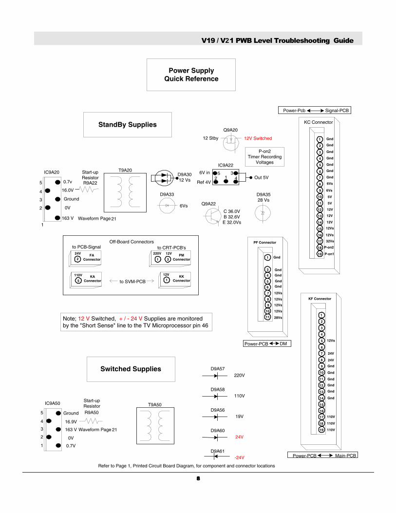
IC9A50
1
2
3
4
5
0.7V
0V
163 V
16.9V
Ground
IC9A20
1
2
3
4
5
163 V
16.0V
Ground
0V
Waveform Page
Waveform Page
StandBy Supplies
T9A50
D9A3012 Vs
Q9A22
C 36.0VB 32.6VE 32.0Vs
D9A3528 Vs
Q9A20
12 Stby 12V Switched
D9A33
6Vs
IC9A22
1235
46V in
Ref 4VOut 5V
D9A57
D9A58
D9A56
D9A60
D9A61
220V
110V
19V
24V
-24V
Switched Supplies
P-on2Timer Recording
Voltages
Note; 12 V Switched, + / - 24 V Supplies are monitoredby the "Short Sense" line to the TV Microprocessor pin 46
1
3
4
5
6
7
8
9
10
11
PF Connector
Gnd
Gnd
Gnd
Gnd
Gnd
12Vs
12Vs
12Vs
12Vs
28Vs1
2
3
4
5
6
7
8
9
10
11
12
13
14
15
16
17
18
19
KF Connector
12Vs
24V
24V
Gnd
Gnd
Gnd
Gnd
Gnd
Gnd
110V
110V
110V
1
2
3
4
5
6
7
8
9
10
11
12
13
14
15
16
17
18
19
KC Connector
Gnd
Gnd
Gnd
Gnd
Gnd
Gnd
Gnd
6Vs
6Vs
5V
5V
12V
12V
12V
12Vs
12Vs
32Vs
P-on2
P-on1
Power-Pcb Signal-PCB
Main-PCBPower-PCB
Power-PCB DM
Power SupplyQuick Reference
21
21
Refer to Page 1, Printed Circuit Board Diagram, for component and connector locations
5KA
Connector
110V
2FA
Connector
24V
1 3PM
Connector
220V 12V
to CRT-PCB's
1KK
Connector
12V
to SVM-PCB
to PCB-SignalOff-Board Connectors
R9A22
Start-upResistor
Start-upResistorR9A50
T9A20
0.7v
V19 / V21 PWB Level Troubleshooting Guide
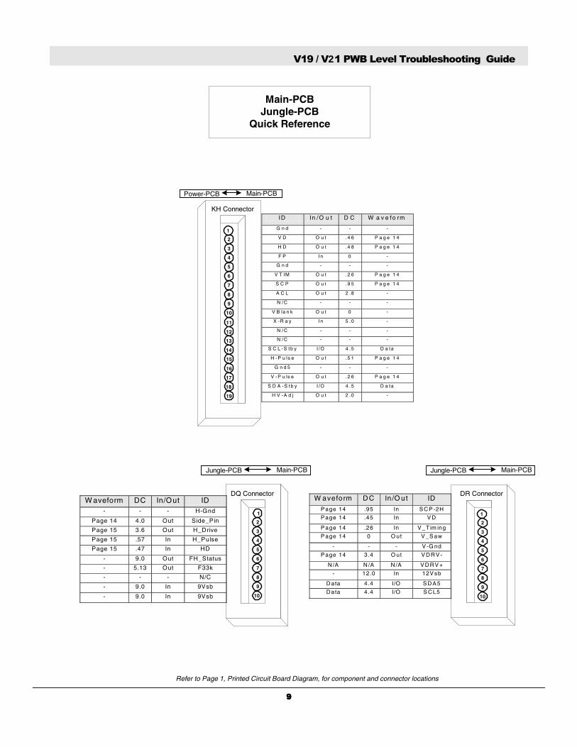
9999
1
2
3
4
5
6
7
8
9
10
11
12
13
14
15
16
17
18
19
KH Connector
Main-PCBPower-PCB
ID In /O u t D C W a v e fo rm
G n d - - -
V D O u t . 4 6 P a g e 1 4
H D O u t . 4 8 P a g e 1 4
F P In 0 -
G n d - - -
V T IM O u t . 2 6 P a g e 1 4
S C P O u t . 9 5 P a g e 1 4
A C L O u t 2 .8 -
N /C - - -
V B la n k O u t 0 -
X -R a y In 5 .0 -
N /C - - -
N /C - - -
S C L -S tb y I /O 4 .5 D a ta
H -P u ls e O u t .5 1 P a g e 1 4
G n d 5 - - -
V -P u ls e O u t . 2 6 P a g e 1 4
S D A -S tb y I /O 4 .5 D a ta
H V -A d j O u t 2 .0 -
1
2
3
4
5
6
7
8
9
10
1
2
3
4
5
6
7
8
9
10
W aveform D C In/O ut ID
P age 14 .95 In S C P -2H
P age 14 .45 In V D
P age 14 .26 In V _T im ing
P age 14 0 O ut V _S aw
- - - V -G nd
P age 14 3.4 O ut V D R V -
N /A N /A N /A V D R V +
- 12.0 In 12V sb
D ata 4.4 I/O S D A 5
D ata 4.4 I/O S C L5
DR Connector
Jungle-PCB Main-PCB
W aveform DC In/Out ID - - - H-Gnd
Page 14 4.0 Out Side_Pin
Page 15 3.6 Out H_Drive
Page 15 .57 In H_Pulse
Page 15 .47 In HD
- 9.0 Out FH_Status
- 5.13 Out F33k
- - - N/C
- 9.0 In 9Vsb
- 9.0 In 9Vsb
DQ Connector
Main-PCBJungle-PCB
Quick Reference
Jungle-PCB Main-PCB
Refer to Page 1, Printed Circuit Board Diagram, for component and connector locations
V19 / V21 PWB Level Troubleshooting Guide
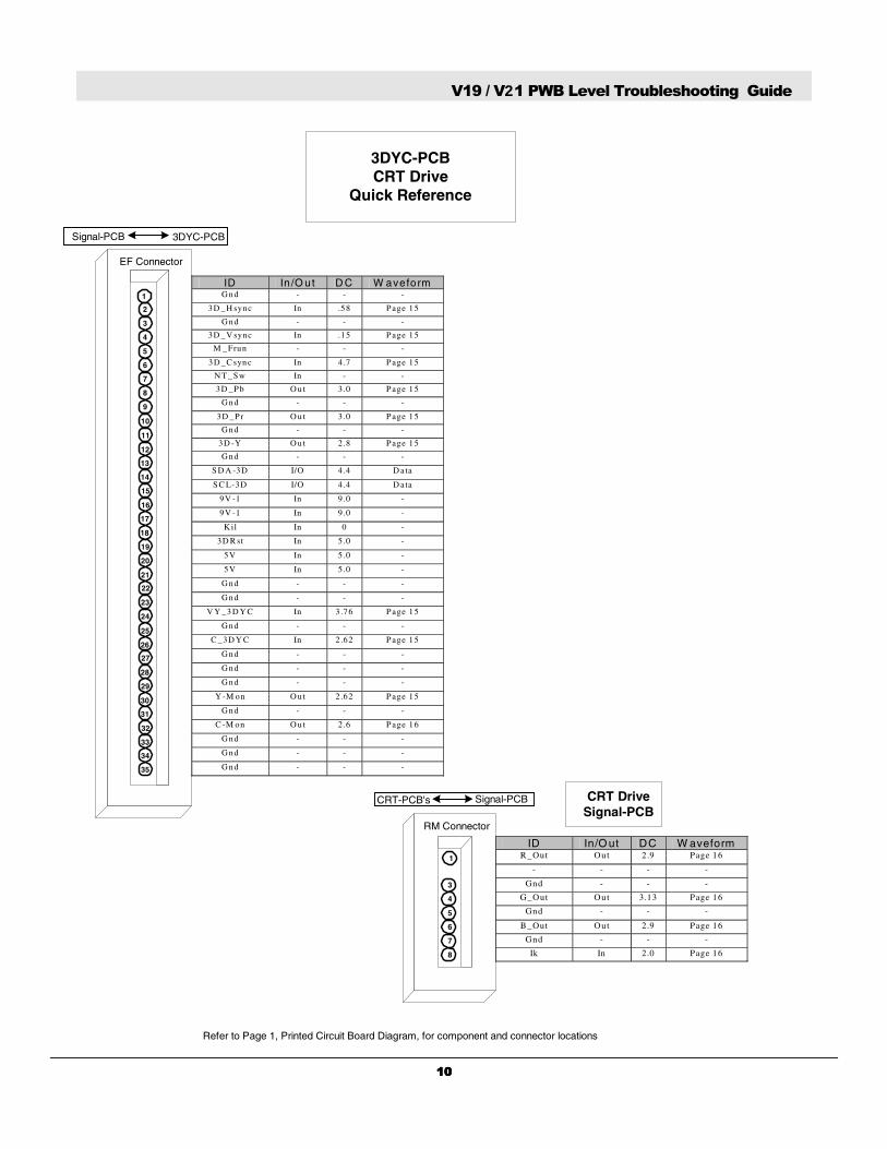
10101010
1
2
3
4
5
6
7
8
9
10
11
12
13
14
15
16
17
18
19
20
21
22
23
24
25
26
27
28
29
30
31
32
33
34
35
EF Connector
ID In /O ut D C W aveform G n d - - -
3D _H sync In .58 Page 1 5
G n d - - -
3D _V sync In .15 Page 1 5
M _ Frun - - -
3D _C syn c In 4 .7 Page 1 5
N T_ Sw In - -
3D _Pb O u t 3 .0 Page 1 5
G n d - - -
3D _Pr O u t 3 .0 Page 1 5
G n d - - -
3D -Y O u t 2 .8 Page 1 5
G n d - - -
SD A -3D I/O 4 .4 D a ta
SC L-3D I/O 4 .4 D a ta
9V -1 In 9 .0 -
9V -1 In 9 .0 -
K il In 0 -
3D R st In 5 .0 -
5V In 5 .0 -
5V In 5 .0 -
G n d - - -
G n d - - -
V Y _3 D Y C In 3 .76 Page 1 5
G n d - - -
C _3D Y C In 2 .62 Page 1 5
G n d - - -
G n d - - -
G n d - - -
Y -M on O u t 2 .62 Page 1 5
G n d - - -
C -M on O u t 2 .6 Page 1 6
G n d - - -
G n d - - -
G n d - - -
1
3
4
5
6
7
8
RM Connector
ID In/O ut DC W aveform R_Out Out 2.9 Page 16
- - - -
Gnd - - -
G_Out Out 3.13 Page 16
Gnd - - -
B_Out Out 2.9 Page 16
Gnd - - -
Ik In 2.0 Page 16
CRT DriveSignal-PCB
3DYC-PCBSignal-PCB
CRT-PCB's Signal-PCB
3DYC-PCBCRT Drive
Quick Reference
Refer to Page 1, Printed Circuit Board Diagram, for component and connector locations
V19 / V21 PWB Level Troubleshooting Guide
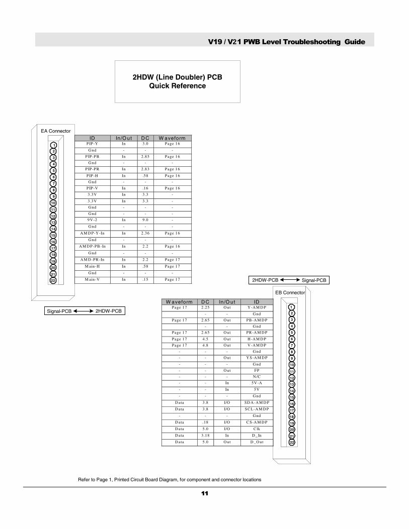
11111111
1
2
3
4
5
6
7
8
9
10
11
12
13
14
15
16
17
18
19
20
21
22
EA Connector
ID In/O ut D C W aveform P IP-Y In 3 .0 Page 16
G nd - - -
P IP-PB In 2 .85 Page 16
G nd - - -
P IP-PR In 2 .83 Page 16
P IP-H In .58 Page 16
G nd - - -
P IP-V In .16 Page 16
3 .3V In 3 .3 -
3 .3V In 3 .3 -
G nd - - -
G nd - - -
9V -2 In 9 .0 -
G nd - - -
A M D P-Y -In In 2 .36 Page 16
G nd - - -
A M D P-PB -In In 2 .2 Page 16
G nd - - -
A M D -PR -In In 2 .2 Page 17
M ain-H In .58 Page 17
G nd - - -
M ain-V In .15 Page 17
1
2
3
4
5
6
7
8
9
10
11
12
13
14
15
16
17
18
19
20
21
22
W aveform D C In/O ut ID Page 17 2 .25 O ut Y -A M D P
- - G nd
Page 17 2 .65 O ut PB -A M D P
- - G nd
Page 17 2 .65 O ut PR -A M D P
Page 17 4 .5 O ut H -A M D P
Page 17 4 .8 O ut V -A M D P
- - - G nd
- - O ut Y S-A M D P
- - - G nd
- - O ut FP
- - - N /C
- - In 5V -A
- - In 5V
- - - G nd
D ata 3 .8 I/O SD A -A M D P
D ata 3 .8 I/O SC L-A M D P
- - - G nd
D ata .18 I/O C S-A M D P
D ata 5 .0 I/O C lk
D ata 3 .18 In D _ In
D ata 5 .0 O ut D _O ut
EB Connector
2HDW-PCB Signal-PCB
2HDW-PCBSignal-PCB
2HDW (Line Doubler) PCBQuick Reference
Refer to Page 1, Printed Circuit Board Diagram, for component and connector locations
V19 / V21 PWB Level Troubleshooting Guide
12121212
1
2
3
4
5
6
7
8
9
10
11
12
13
VA Connector
ID In/Out DC W aveform DM -G Out 2 .4 Page 17
Gnd - - -
DM -B Out 2 .4 Page 17
Gnd - - -
DM -R Out 2 .4 Page 17
Gnd - - -
DM -H Out 3 .11 Page 17
DM -V Out 3 .22 Page 18
Gnd - - -
DSP-H In .44 Page 18
DSP-V In 0 Page 18
Gnd - - -
M asking Out 0 High = O SD on
W aveform DC In/O ut ID Page 18 .9 In M ain -Y
- - - Gnd
Page 18 2.2 In M ain-CB
- - - Gnd
Page 18 2.2 In M ain-CR
- - - Gnd
Page 18 4.7 In M ain_Sync
- - - N/C
- - - Gnd
- 5 .0 Out TV_R eset
- - - Gnd
Page* 18 .9* Out Y-DM
- - - Gnd
Page* 18 .9* Out C-DM
- - - Gnd
1
2
3
4
5
6
7
8
9
10
11
12
13
14
15
DB Connector
* Available in HDTV orOSD Modes Only
1
2
3
4
5
6
7
8
9
10
11
12
13
14
DA Connector
ID In/Out DC W aveform
L-DM Out HD Audio
Gnd - - -
R -DM Out HD Audio
Gnd - - -
DM _Reset In 0V -
Powergood Out 0V
TV -DM _R TS I/O Data
TV -DM _C TS I/O Data
DM _Rxd I/O Data
Gnd - - -
TV-DM _Txd I/O Data
DM D etect Out 0V
IR_In_Busy Out Data
IR_Out_ENA In Data
1
3
4
5
6
7
8
9
10
11
PF Connector
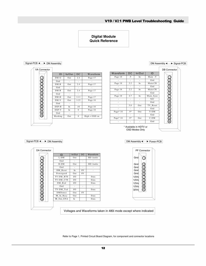
Voltages and Waveforms taken in 480i mode except where indicated
Signal-PCB DM Assembly
Signal-PCB DM Assembly DM Assembly Power-PCB
Digital ModuleQuick Reference
Signal-PCBDM Assembly
Gnd
GndGndGndGnd
12Vs12Vs12Vs12Vs32Vs
Refer to Page 1, Printed Circuit Board Diagram, for component and connector locations
V19 / V21 PWB Level Troubleshooting Guide
13131313
1
2
3
4
5
6
7
8
9
10
11
12
13
14
15
16
17
18
19
20
21
22
23
24
25
26
27
28
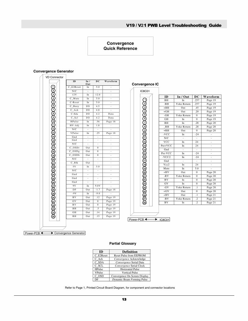
Convergence IC
IC8C01
ID In / Out DC Waveform BH In .257 Page 19
-BH Yoke Return .257 Page 19
+BH Out .45 Page 19
+GH Out .20 Page 19
-GH Yoke Return 0 Page 19
GH In 0 Page 19
RH In .28 Page 20
_RH Yoke Return .28 Page 20
+RH Out 0 Page 20
-VCC In -24 -
N/C - - -
VCC In 24 -
Pre+VCC In 24 -
Gnd - - -
Pre-VCC In -24 -
-VCC2 In -24 -
Gnd - - -
Vcc2 In 24 -
Mute In 5.0 -
+RV Out 0 Page 20
-RV Yoke Return 0 Page 20
RV In 0 Page 20
GV In 0 Page 20
-GV Yoke Return .1 Page 20
+GV Out 0 Page 20
+BV Out .1 Page 21
-BV Yoke Return .2 Page 21
BV In .2 Page 21
ID Definition C_E2Reset Reset Pulse from EEPROM C_Ack Convergence Acknowledge C_SDA Convergence Serial Data C_SCL Convergence Serial Clock HPulse Horizontal Pulse VPulse Vertical Pulse C_OSD Convergence On Screen Display DF Dynamic Beam Forming Pulse
1
2
3
4
5
6
7
8
9
10
11
12
13
14
15
16
17
18
19
20
21
22
23
24
25
26
27
28
29
30
31
32
33
34
35
Convergence Generator
VD ConnectorID In /
O ut D C W aveform
C _E2R eset In 5 .0 -
N /C - - -
12V In 12.0 -
C _M ute In 5 .0 -
C -R eset In 5 .0 -
C _B usy I/O 4 .5 -
C _Ack I/O 4 .8 -
C -Sda I/O 4 .2 D ata
C _Scl I/O 4 .2 D ata
H Pulse In .56 Page 18
H V -Adj In 1 .8 -
N /C - - -
V Pu lse In .25 Page 18
Gnd - - - Gnd - - -
N /C - - -
C _O SD r O u t 0 -
C _O SD g O ut 0 -
C _O SD b O ut 0 -
N /C - - -
C _B lk O u t - -
5V In 5 .0 -
N /C - - -
Gnd - - -
Gnd - - -
Gnd - - -
9V In 9 .0V -
D F O ut -1 .7 Page 18
-9V In -9 .0 -
B V O ut .12 Page 19
GV O ut 0 Page 19
R V O ut 0 Page 19
B H O ut .5 Page 19
GH O ut .14 Page 19
R H O ut .15 Page 19
Partial Glossary
Convergence GeneratorPower-PCB
IC8C01Power-PCB
ConvergenceQuick Reference
Refer to Page 1, Printed Circuit Board Diagram, for component and connector locations
V19 / V21 PWB Level Troubleshooting Guide
14141414
V19 / V21 PWB Level Troubleshooting Guide
15151515
V19 / V21 PWB Level Troubleshooting Guide
16161616
V19 / V21 PWB Level Troubleshooting Guide
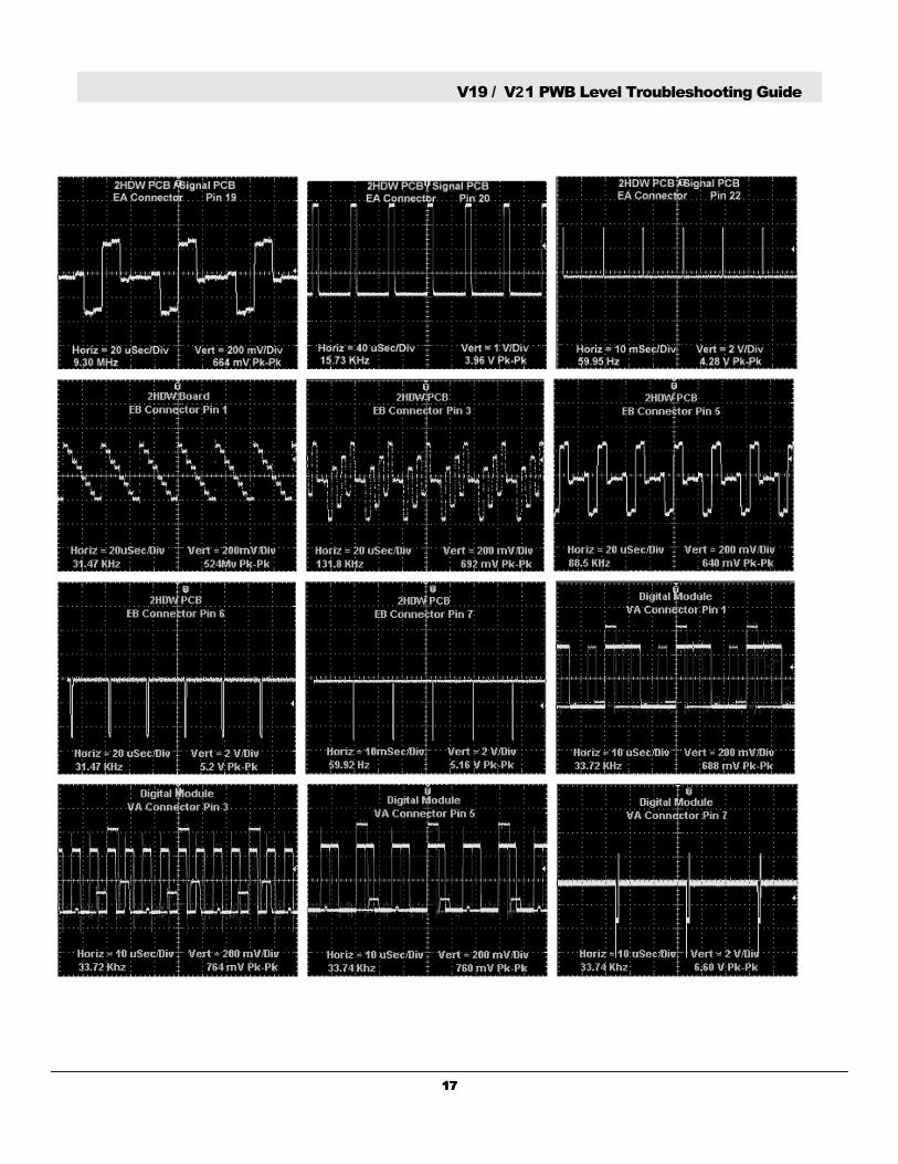
17171717
V19 / V21 PWB Level Troubleshooting Guide
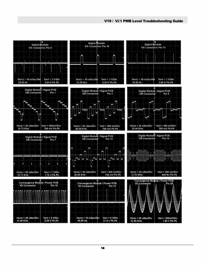
18181818
V19 / V21 PWB Level Troubleshooting Guide
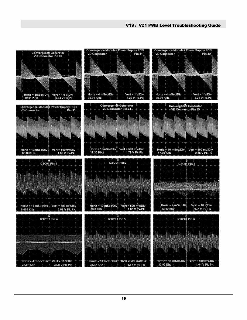
19191919
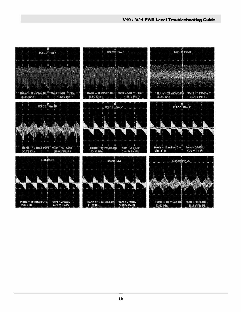
V19 / V21 PWB Level Troubleshooting Guide
2020 20191919
V19 / V21 PWB Level Troubleshooting Guide