Qucs Simulation of SPICE Netlists - GitHub Pagesguitorri.github.io/qucs-web/docs/spicetoqucs.pdf ·...
29
Qucs A Tutorial Qucs Simulation of SPICE Netlists Mike Brinson Copyright c 2007 Mike Brinson <[email protected]> Permission is granted to copy, distribute and/or modify this document under the terms of the GNU Free Documentation License, Version 1.1 or any later version published by the Free Software Foundation. A copy of the license is included in the section entitled ”GNU Free Documentation License”.
Transcript of Qucs Simulation of SPICE Netlists - GitHub Pagesguitorri.github.io/qucs-web/docs/spicetoqucs.pdf ·...

Qucs
A Tutorial
Qucs Simulation of SPICE Netlists
Mike Brinson
Copyright c© 2007 Mike Brinson <[email protected]>
Permission is granted to copy, distribute and/or modify this document under the terms ofthe GNU Free Documentation License, Version 1.1 or any later version published by theFree Software Foundation. A copy of the license is included in the section entitled ”GNUFree Documentation License”.

Introduction
During the 1960’s and 70’s, the academic community worked tirelessly to develop computersimulation programs that could act as aids in the process of circuit design. One of the bestknown of these programs is SPICE1. First released in 1972 by the University of Californiaat Berkeley, SPICE has become an industrial standard circuit simulator. Qucs is a moderncircuit simulation program which attempts to bring together a range of established andemerging circuit simulation technologies to form a ”Quite Universal Circuit Simulator”. Al-though not yet finished, a substantial part of the central core of the package is functioning,allowing it to be used as a simulation engine for the analysis and design of real circuits.Many of the basic circuit components and simulation domains found in SPICE are alsoavailable in Qucs. Over the last three decades the SPICE simulation circuit netlist lan-guage has become a standard for describing, interchanging and publishing semiconductordevice models and circuit data. Today, most semiconductor device manufacturers provideSPICE models or subcircuit netlists for their discreet components and integrated circuits.One area where Qucs and SPICE differ significantly is in their circuit file netlist formatswhich are very different2. Qucs cannot directly simulate standard SPICE circuit netlistsbut requires them to be converted to their Qucs equivalent prior to simulation. The pur-pose of this tutorial note is to introduce readers to a number of techniques that allowSPICE netlists to be simulated by Qucs, secondly to indicate the limitations of the currentSPICE to Qucs netlist conversion process, and finally to present a preview of how Qucs islikely develop in the future in the area of SPICE netlist compatibility.
The basic SPICE netlist format
SPICE simulation input data are text files which describe circuit structure, component dataand requested simulation tasks for the circuit who’s performance is being simulated. Suchtext files form the fundamental input data to the SPICE simulation engine, and normallyinclude:
• A title statement
• Circuit node names
• Circuit element values
• Voltage and current source descriptions
• Analysis command statements
1The origins and background to the development of the SPICE simulator are described by Ronald A.Rohrer in Circuit Simulation - the early years, illuminating SPICE’s strengths, uncovering weaknesses,and projecting its future, IEEE Circuits and Devices, 1992, pp 32-37.
2The Qucs netlist grammar is defined in appendix A1, of the Qucs Technical Papers.
1

• Output data statements
• Other command statements
In SPICE 23circuit node names (nets) are identified by integers numbered from 0 to 9999.SPICE 34 allows a mixture of letters and numbers for node names. All circuit nodes musthave a DC path to ground. Ground node is always node 0 and is considered global. Circuitelement values are expressed as integers or real numbers in scientific notation, for example5, 0.5e1 5.0, or in engineering notation using suffixes. The available SPICE suffixes are f =1e-15 (femto), p = 1e-12 (pico), n = 1e-9 (nano), u = 1e-6 (micro), mil = 25e-6, m = 1e-3(milli), k = 1e3 (kilo), meg = 1e6 (mega), g = 1e9 (giga) and t = 1e12 (tera). Componentunit abbreviations are allowed in circuit value descriptions. However, these must not beseparated from their associated values by spaces. Commonly used unit abbreviations areV = Volt, A = Amps. Hz = Hertz, ohm = Ohm(Ω), H = Henry, F = Farad and deg =Degree. SPICE input data files have the following format:
1. Title
2. * starts a comment line
3. Circuit description
4. Simulation directives
5. Data output directives
6. .end
A typical SPICE input data file for a discreet component circuit is shown in Fig. 1. Inthis netlist all nodes are shown numbered, following the SPICE 2 node naming convention.Also the power supply, AC input signal generator and output load are not included. Essen-tially, the netlist shown in Fig. 1 represents the amplifier without any external componentsconnected to it. Although Qucs cannot directly simulate SPICE netlists the software doescontain a SPICE to Qucs netlist conversion program called QUCSCONV. This routinetakes as input a SPICE netlist file and outputs an equivalent Qucs formatted netlist file.The Qucs netlist file can be read and simulated by the Qucs simulation engine. To make theprocess transparent, and indeed straightforward for users, the conversion stage in simulat-ing SPICE netlist files5 has been automated via the Qucs GUI simulate command (F2 key).
3A guide to SPICE 2 features and simulation data format is given in SPICE Version 2G User’s Guide,A Vladimirescu, Kaihe Zhang, A.R. Newton, D. O. Pederson and A. Sangiovanni-Vincentelli, August1981, Department of Electrical Engineering and Computer Sciences, University of California, Berkeley,Ca., 94720, US.
4See SPICE 3 Version 3F User’s Manual, B. Johnson, T. Quarles,A.R. Newton, D. O. Pederson andA. Sangiovanni-Vincentelli, October 1992, Department of Electrical Engineering and Computer Sciences,University of California, Berkeley, Ca., 94720, US.
5For convenience SPICE netlist files are often denoted with the extention cir and stored in a Qucsproject under the other category.
2
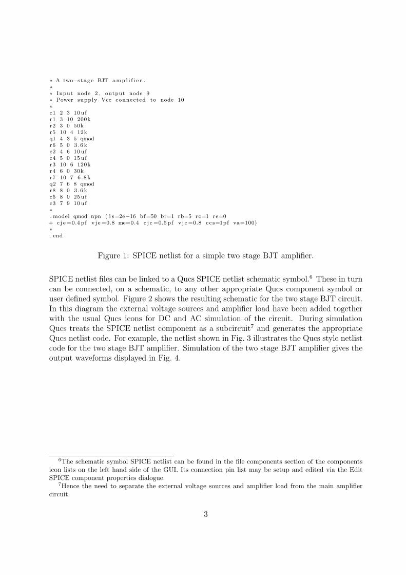
∗ A two−s tage BJT amp l i f i e r .∗∗ Input node 2 , output node 9∗ Power supply Vcc connected to node 10∗c1 2 3 10 ufr1 3 10 200kr2 3 0 50kr5 10 4 12kq1 4 3 5 qmodr6 5 0 3 .6 kc2 4 6 10 ufc4 5 0 15 ufr3 10 6 120kr4 6 0 30kr7 10 7 6 .8 kq2 7 6 8 qmodr8 8 0 3 .6 kc5 8 0 25 ufc3 7 9 10 uf∗. model qmod npn ( i s=2e−16 bf=50 br=1 rb=5 rc=1 re=0+ c j e =0.4 pf v j e =0.8 me=0.4 c j c =0.5 pf v j c =0.8 cc s=1pf va=100)∗. end
Figure 1: SPICE netlist for a simple two stage BJT amplifier.
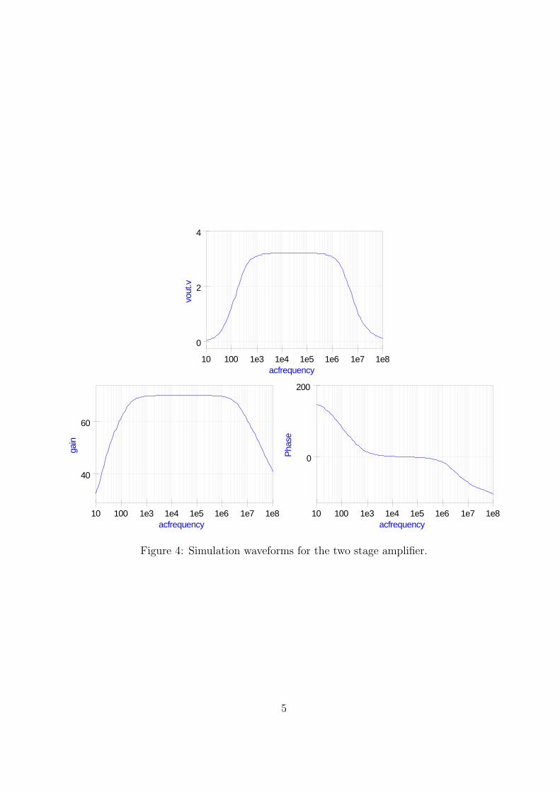
SPICE netlist files can be linked to a Qucs SPICE netlist schematic symbol.6 These in turncan be connected, on a schematic, to any other appropriate Qucs component symbol oruser defined symbol. Figure 2 shows the resulting schematic for the two stage BJT circuit.In this diagram the external voltage sources and amplifier load have been added togetherwith the usual Qucs icons for DC and AC simulation of the circuit. During simulationQucs treats the SPICE netlist component as a subcircuit7 and generates the appropriateQucs netlist code. For example, the netlist shown in Fig. 3 illustrates the Qucs style netlistcode for the two stage BJT amplifier. Simulation of the two stage BJT amplifier gives theoutput waveforms displayed in Fig. 4.
6The schematic symbol SPICE netlist can be found in the file components section of the componentsicon lists on the left hand side of the GUI. Its connection pin list may be setup and edited via the EditSPICE component properties dialogue.
7Hence the need to separate the external voltage sources and amplifier load from the main amplifiercircuit.
3

spice
2 9
10
Ref
X1File=stoq_nl1.cir
V1U=1m V
V2U=15 V
RLR=10k Ohm
dc simulation
DC1
ac simulation
AC1Type=logStart=10 HzStop=100 MHzPoints=200
Equation
Eqn1Phase=phase(vout.v)gain=dB(vout.v/vin.v)
vin
vout
Figure 2: Qucs schematic for the two stage amplifier represented by the SPICE netlistshown in Fig. 1.
. Def : s t o q n l 1 c i r net2 net9 net10 r e fC:C3 net7 net9 C=”10uF”C:C5 net8 r e f C=”25uF”R:R8 net8 r e f R=”3.6k”BJT:Q2 net6 net7 net8 r e f Type=”npn” I s =”2e−16” Bf=”50” Br=”1”
Rb=”5” Rc=”1” Re=”0” Cje =”0.4pF”Vje =”0.8” Mje=”0.4” Cjc =”0.5pF”Vjc =”0.8” Cjs=”1pF” Vaf=”100” Nf=”1” Nr=”1” I k f =”0” Ikr =”0” Var=”0”I s e =”0” Ne=”1.5” I s c =”0” Nc=”2” Rbm=”0” Irb =”0” Mjc=”0.33” Xcjc=”1”Vjs =”0.75” Mjs=”0” Fc=”0.5” Vtf=”0” Tf=”0” Xtf=”0” I t f =”0” Tr=”0”
R:R7 net10 net7 R=”6.8k”R:R4 net6 r e f R=”30k”R:R3 net10 net6 R=”120k”C:C4 net5 r e f C=”15uF”C:C2 net4 net6 C=”10uF”R:R6 net5 r e f R=”3.6k”BJT:Q1 net3 net4 net5 r e f Type=”npn” I s =”2e−16” Bf=”50” Br=”1”
Rb=”5” Rc=”1” Re=”0” Cje =”0.4pF”Vje =”0.8” Mje=”0.4” Cjc =”0.5pF”Vjc =”0.8” Cjs=”1pF” Vaf=”100” Nf=”1” Nr=”1” I k f =”0” Ikr =”0” Var=”0”I s e =”0” Ne=”1.5” I s c =”0” Nc=”2” Rbm=”0” Irb =”0” Mjc=”0.33” Xcjc=”1”Vjs =”0.75” Mjs=”0” Fc=”0.5” Vtf=”0” Tf=”0” Xtf=”0” I t f =”0” Tr=”0”
R:R5 net10 net4 R=”12k”R:R2 net3 r e f R=”50k”R:R1 net3 net10 R=”200k”C:C1 net2 net3 C=”10uF”
. Def : End
Figure 3: Qucs format netlist for the two stage BJT amplifier: NOTE -In this listing theentries for Q1 and Q2 have been edited so that they fit on the text page.
4
10 100 1e3 1e4 1e5 1e6 1e7 1e8
40
60
acfrequency
gain
10 100 1e3 1e4 1e5 1e6 1e7 1e8
0
200
acfrequency
Pha
se
10 100 1e3 1e4 1e5 1e6 1e7 1e8
0
2
4
acfrequency
vout
.v
Figure 4: Simulation waveforms for the two stage amplifier.
5

Defining symbols for Qucs SPICE netlist components
Qucs automatically generates the symbol for a SPICE netlist component and does notallow users to edit the resulting symbol. One of the disadvantage of this feature is that theplacement of the symbol input and output pins may be in a position which is contrary toaccepted use or signal flow direction. To overcome this limitation a user defined symbol maybe constructed where the SPICE netlist component is embedded within the new symbol.Figure 5 illustrates such a symbol for the two stage BJT amplifier and the resulting Qucsnetlist for the new symbol is shown in Fig. 6. From Fig. 6 we observe that embedding aSPICE netlist symbol, within a user defined symbol, introduces an additional subcircuitcall in the resulting Qucs netlist; this is probably a small price to pay for the conveniencethat a user defined symbol brings to the overall simulation process.
spice
2 9
10
Ref
X1File=stoq_nl1.cir
P_IN1
P_OUT1
P_VCC1
VCC
SUB1
Figure 5: User defined symbol for the two stage BJT amplifier.
6

. Def : s toq f i g5 amp net0 net1 net2Sub :X1 net0 net1 net2 gnd Type=”s t o q n l 1 c i r ”. Def : End
. Def : s t o q n l 1 c i r net2 net9 net10 r e fC:C3 net7 net9 C=”10uF”C:C5 net8 r e f C=”25uF”R:R8 net8 r e f R=”3.6k”BJT:Q2 net6 net7 net8 r e f Type=”npn” I s =”2e−16” Bf=”50” Br=”1”
Rb=”5” Rc=”1” Re=”0” Cje =”0.4pF”Vje =”0.8” Mje=”0.4” Cjc =”0.5pF”Vjc =”0.8” Cjs=”1pF” Vaf=”100” Nf=”1” Nr=”1” I k f =”0” Ikr =”0” Var=”0”I s e =”0” Ne=”1.5” I s c =”0” Nc=”2” Rbm=”0” Irb =”0” Mjc=”0.33” Xcjc=”1”Vjs =”0.75” Mjs=”0” Fc=”0.5” Vtf=”0” Tf=”0” Xtf=”0” I t f =”0” Tr=”0”
R:R7 net10 net7 R=”6.8k”R:R4 net6 r e f R=”30k”R:R3 net10 net6 R=”120k”C:C4 net5 r e f C=”15uF”C:C2 net4 net6 C=”10uF”R:R6 net5 r e f R=”3.6k”
BJT:Q1 net3 net4 net5 r e f Type=”npn” I s =”2e−16” Bf=”50” Br=”1”Rb=”5” Rc=”1” Re=”0” Cje =”0.4pF”Vje =”0.8” Mje=”0.4” Cjc =”0.5pF”Vjc =”0.8” Cjs=”1pF” Vaf=”100” Nf=”1” Nr=”1” I k f =”0” Ikr =”0” Var=”0”I s e =”0” Ne=”1.5” I s c =”0” Nc=”2” Rbm=”0” Irb =”0” Mjc=”0.33” Xcjc=”1”Vjs =”0.75” Mjs=”0” Fc=”0.5” Vtf=”0” Tf=”0” Xtf=”0” I t f =”0” Tr=”0”
R:R5 net10 net4 R=”12k”R:R2 net3 r e f R=”50k”R:R1 net3 net10 R=”200k”C:C1 net2 net3 C=”10uF”
. Def : End
Figure 6: Qucs format netlist for the two stage BJT amplifier represented by a user definedsymbol: NOTE -In this listing the entries for Q1 and Q2 have been edited so that they fiton the text page.
7

Handling SPICE subcircuits
Although Qucs treats SPICE netlist components as subcircuits the SPICE to Qucs netlistconversion process still allows SPICE subcircuits to be defined within the SPICE file beingconverted. Such subcircuits then become local subcircuits to the SPICE netlist componentto which they are attached. This allows complex circuits consisting of many related, butoften different, circuit blocks to be represented by a single symbol in a Qucs schematic.In such cases the resulting symbol represents a true subsection of an entire circuit ratherthan a simple single circuit function subcircuit. To demonstrate this feature consider thefollowing examples; (1) a multisection LC delay line and (2) a CMOS ring counter.
Subcircuit example 1: a multisection LC delay line
The SPICE netlist for a ten section LC passive delay line is shown in Fig. 7. In thislisting each LC delay section is represented by a SPICE subcircuit and these sections areconnected in series to form the overall delay line. Figures 8 and 9 present the resultingQucs netlist and generated waveforms obtained with the test circuit shown in Fig. 10.
Subcircuit example 2: a two section CMOS ring counter
Subcircuit example one only contains a single local subcircuit. The next example demon-strates how SPICE listings with more than one subcircuit are handled by Qucs. Suchcircuits are representative of more complex electronic systems which form easily identifi-able subsystem blocks.8 Fig. 11 shows the SPICE netlist for a simple two section CMOSring counter. This circuit is modelled at discreet component level and uses basic level oneMOS parameters to define the MOS transistors. These are then combined to form NANDand NOR subcircuits. Again for completeness the resulting Qucs netlist is shown in Fig. 12together with a typical set of counter input and output signal waveforms, Fig. 13.
8One significant advantage that Qucs has when compared to netlist entry only circuit simulators is thatit is possible the define schematic symbols for subsystem blocks that comprise discreet components andone or more local subcircuits. These may then be employed like any other Qucs symbols when constructingcircuit schematics.
8

∗ Z0 = 320 Ohm.∗. subckt l c n1 n2l 1 n1 n2 10uhc1 n2 0 10 pf. ends∗r s n9 n10 320ohmx1 n10 n11 l cx2 n11 n12 l cx3 n12 n13 l cx4 n13 n14 l cx5 n14 n15 l cx6 n15 n16 l cx7 n16 n17 l cx8 n17 n18 l cx9 n18 n19 l cx10 n19 n20 l cr l n20 0 320ohm. end
Figure 7: SPICE netlist for a ten section LC delay line..
. Def : s t o q f i g 1 0 a net0 net10 net1 net2 net3 net4net5 net6 net7 net8 net9
Sub :X1 net0 net10 net1 net2 net3 net4net5 net6 net7 net8 net9 gnd Type=”t e s t 3 p p c i r ”
. Def : End
. Def : t e s t 3 p p c i r netN9 netN11 netN12 netN13 netN14netN15 netN16 netN17 netN18 netN19 netN20 r e f
R:RL netN20 r e f R=”320Ohm”Sub : X10 r e f netN19 netN20 Type=”LC”Sub :X9 r e f netN18 netN19 Type=”LC”Sub :X8 r e f netN17 netN18 Type=”LC”Sub :X7 r e f netN16 netN17 Type=”LC”Sub :X6 r e f netN15 netN16 Type=”LC”Sub :X5 r e f netN14 netN15 Type=”LC”Sub :X4 r e f netN13 netN14 Type=”LC”Sub :X3 r e f netN12 netN13 Type=”LC”Sub :X2 r e f netN11 netN12 Type=”LC”Sub :X1 r e f netN10 netN11 Type=”LC”R:RS netN9 netN10 R=”320Ohm”. Def :LC r e f netN1 netN2L : L1 netN1 netN2 L=”10uH”C:C1 netN2 r e f C=”10pF”. Def : End
. Def : End
Figure 8: Qucs netlist for a 10 section LC delay line: NOTE -In this listing the entries forthe .Def statements have been edited so that they fit on the text page.
9

0 1e-8 2e-8 3e-8 4e-8 5e-8 6e-8 7e-8 8e-8 9e-8 1e-7 1.1e-7 1.2e-7
0
1
timevi
n.V
t
0 1e-8 2e-8 3e-8 4e-8 5e-8 6e-8 7e-8 8e-8 9e-8 1e-7 1.1e-7 1.2e-7
0
0.2
time
v10.
Vt
0 1e-8 2e-8 3e-8 4e-8 5e-8 6e-8 7e-8 8e-8 9e-8 1e-7 1.1e-7 1.2e-7
0
0.2
time
v20.
Vt
0 1e-8 2e-8 3e-8 4e-8 5e-8 6e-8 7e-8 8e-8 9e-8 1e-7 1.1e-7 1.2e-7
0
0.2
time
v30.
Vt
0 1e-8 2e-8 3e-8 4e-8 5e-8 6e-8 7e-8 8e-8 9e-8 1e-7 1.1e-7 1.2e-7
0
0.2
time
v40.
Vt
0 1e-8 2e-8 3e-8 4e-8 5e-8 6e-8 7e-8 8e-8 9e-8 1e-7 1.1e-7 1.2e-7
0
0.2
time
v50.
Vt
0 1e-8 2e-8 3e-8 4e-8 5e-8 6e-8 7e-8 8e-8 9e-8 1e-7 1.1e-7 1.2e-7-0.1
0
0.1
0.2
time
v60.
Vt
0 1e-8 2e-8 3e-8 4e-8 5e-8 6e-8 7e-8 8e-8 9e-8 1e-7 1.1e-7 1.2e-7-0.2
0
0.2
time
v80.
Vt
0 1e-8 2e-8 3e-8 4e-8 5e-8 6e-8 7e-8 8e-8 9e-8 1e-7 1.1e-7 1.2e-7
-0.1
0
0.1
time
v90.
Vt
0 1e-8 2e-8 3e-8 4e-8 5e-8 6e-8 7e-8 8e-8 9e-8 1e-7 1.1e-7 1.2e-7
0
0.05
time
v100
.Vt
0 1e-8 2e-8 3e-8 4e-8 5e-8 6e-8 7e-8 8e-8 9e-8 1e-7 1.1e-7 1.2e-7
0
0.2
time
v70.
Vt
Figure 9: Simulation waveforms for a 10 section LC delay line.
10

V1U1=0 VU2=1 VT1=0T2=5 n
20nS
10nS
40nS
30nS
50nS
60nS
70nS
80nS
90nS
100nS
SUB1
transientsimulation
TR1Type=linStart=0Stop=120 nsIntegrationMethod=GearOrder=6
vin
v10
v20
v30
v40
v50
v60
v70
v80
v90
v100
Figure 10: LC delay line test circuit.
∗ Two stage CMOS r ing counter c i r c u i t .∗x1 1 5 6 nand2x2 1 6 7 nand2x3 3 6 2 nand2x4 2 7 3 nand2x5 1 2 8 nor2x6 1 8 9 nor2x7 5 8 4 nor2x8 4 9 5 nor2∗. model modp pmos( vto=−1 kp=10u+ cgdo=0.2n cgso =0.2n cgbo=2n). model modn nmos( vto=1 kp=10u+ cgdo=0.2n cgso =0.2n cgbo=2n)∗. subckt nand2 1 2 3m1 3 1 4 4 modp w=40u l=5um2 3 2 4 4 modp w=40u l=5um3 5 1 0 0 modn w=20u l=5um4 3 2 5 5 modn w=20u l=5uc1 1 0 10pc2 2 0 10pvcc 4 0 pu l s e ( 0 5 0 1ns 1ns 1 2). ends∗. subckt nor2 1 2 3m1 4 1 7 7 modp w=40u l=5um2 3 2 4 4 modp w=40u l=5um3 3 2 0 0 modn w=20u l=5um4 3 1 0 0 modn w=20u l=5uc1 1 0 10pc2 2 0 10pvcc 7 0 pu l s e ( 0 5 0 1ns 1ns 1 2). ends. end
Figure 11: SPICE netlist for a two section CMOS ring counter.
11

# Qucs 0 . 0 . 1 1 /media/hda2/OPAMP templates/ t e s t s t o q f i g 1 1 a . sch. Def : s t o q f i g 1 1 a c i r net1 net4 r e f
. Def :NOR2 r e f net1 net2 net3Vpulse :VCC net7 cnet0 U1=”0” U2=”5” T1=”0” Tr=”1ns ” Tf=”1ns ” T2=”1”MOSFET:M1 net1 net4 net7 net7 Type=”p f e t ” W=”40u” L=”5u” Vt0=”−1”
Kp=”10u” Cgdo=”0.2n” Cgso=”0.2n” Cgbo=”2n” I s =”1e−14” N=”1”Lambda=”0” Gamma=”0” Phi =”0.6”
MOSFET:M2 net2 net3 net4 net4 Type=”p f e t ” W=”40u” L=”5u” Vt0=”−1”Kp=”10u” Cgdo=”0.2n” Cgso=”0.2n” Cgbo=”2n” I s =”1e−14” N=”1”Lambda=”0” Gamma=”0” Phi =”0.6”
MOSFET:M3 net2 net3 r e f r e f Type=”n f e t ” W=”20u” L=”5u” Vt0=”1”Kp=”10u” Cgdo=”0.2n” Cgso=”0.2n” Cgbo=”2n” I s =”1e−14” N=”1”Lambda=”0” Gamma=”0” Phi =”0.6”
MOSFET:M4 net1 net3 r e f r e f Type=”n f e t ” W=”20u” L=”5u” Vt0=”1”Kp=”10u” Cgdo=”0.2n” Cgso=”0.2n” Cgbo=”2n” I s =”1e−14” N=”1”Lambda=”0” Gamma=”0” Phi =”0.6”
C:C1 net1 r e f C=”10p”C:C2 net2 r e f C=”10p”Vdc :VCC cnet0 r e f U=”0”. Def : End. Def :NAND2 r e f net1 net2 net3Vpulse :VCC net4 cnet1 U1=”0” U2=”5” T1=”0” Tr=”1ns ” Tf=”1ns ” T2=”1”MOSFET:M1 net1 net3 net4 net4 Type=”p f e t ” W=”40u” L=”5u” Vt0=”−1”
Kp=”10u” Cgdo=”0.2n” Cgso=”0.2n” Cgbo=”2n” I s =”1e−14” N=”1”Lambda=”0” Gamma=”0” Phi =”0.6”
MOSFET:M2 net2 net3 net4 net4 Type=”p f e t ” W=”40u” L=”5u” Vt0=”−1”Kp=”10u” Cgdo=”0.2n” Cgso=”0.2n” Cgbo=”2n” I s =”1e−14” N=”1”Lambda=”0” Gamma=”0” Phi =”0.6”
MOSFET:M3 net1 net5 r e f r e f Type=”n f e t ” W=”20u” L=”5u” Vt0=”1”Kp=”10u” Cgdo=”0.2n” Cgso=”0.2n” Cgbo=”2n” I s =”1e−14” N=”1”Lambda=”0” Gamma=”0” Phi =”0.6”
MOSFET:M4 net2 net3 net5 net5 Type=”n f e t ” W=”20u” L=”5u” Vt0=”1”Kp=”10u” Cgdo=”0.2n” Cgso=”0.2n” Cgbo=”2n” I s =”1e−14” N=”1”Lambda=”0” Gamma=”0” Phi =”0.6”
C:C1 net1 r e f C=”10p”C:C2 net2 r e f C=”10p”Vdc :VCC cnet1 r e f U=”0”. Def : EndSub :X8 r e f net4 net9 net5 Type=”NOR2”Sub :X7 r e f net5 net8 net4 Type=”NOR2”Sub :X6 r e f net1 net8 net9 Type=”NOR2”Sub :X5 r e f net1 net2 net8 Type=”NOR2”Sub :X4 r e f net2 net7 net3 Type=”NAND2”Sub :X3 r e f net3 net6 net2 Type=”NAND2”Sub :X2 r e f net1 net6 net7 Type=”NAND2”Sub :X1 r e f net1 net5 net6 Type=”NAND2”
. Def : EndSub :X1 vin vout gnd Type=”s t o q f i g 1 1 a c i r ”Vrect :V1 vin gnd U=”5 V” TH=”1 us ” TL=”1 us ” Tr=”1 ns ” Tf=”1 ns ” Td=”0 ns ”.TR:TR1 Type=”l i n ” Sta r t =”0” Stop=”30u” Points =”1000” Integrat ionMethod=”Trapezo ida l ”Order=”2” I n i t i a l S t e p =”0.01 ns ” MinStep=”1e−18” MaxIter=”150” r e l t o l =”0.01”ab s t o l =”1 uA” vnto l =”100 uV” Temp=”26.85” LTErelto l=”1e−3” LTEabstol=”1e−4”LTEfactor=”1” So lve r=”CroutLU” relaxTSR=”no ” in i t i a lDC=”yes ” MaxStep=”0”
Figure 12: Qucs netlist for a two section CMOS ring counter: NOTE -In this listing theentries for MOSFETs and transient analysis have been edited so that they fit on the textpage.
12

0 2e-6 4e-6 6e-6 8e-6 1e-5 1.2e-5 1.4e-5 1.6e-5 1.8e-5 2e-5 2.2e-5 2.4e-5 2.6e-5 2.8e-5 3e-5
0
2
4
6
time
vin.
Vt
0 2e-6 4e-6 6e-6 8e-6 1e-5 1.2e-5 1.4e-5 1.6e-5 1.8e-5 2e-5 2.2e-5 2.4e-5 2.6e-5 2.8e-5 3e-5
0
2
4
6
time
vout
.Vt
Figure 13: Two stage CMOS ring counter signal waveforms.
13

Limitations when converting SPICE netlists
Not all SPICE netlists can be converted to Qucs netlist format and simulated by Qucs9.There are a number of reasons for this. The first and most obvious is due to the fact thatsome SPICE components have not been implemented in Qucs yet. Nonlinear controlledvoltage and current sources are an example.10 There are also a number of detailed dif-ferences between the SPICE and Qucs implementation of components common to bothsimulators, one being the lack of PWL features in the Qucs independent voltage and cur-rent sources. A second area that represents a significant limitation, for those readers whoregularly write SPICE netlists as part of their simulation work, is the fact that Qucs con-tains a much greater range of predefined primitive components that are not available ineither the SPICE 2 or SPICE 3 simulators. Perhaps this is not so much a limitation but anindication of the current development effort being put into Qucs by the development team.As the development of Qucs progresses it is expected that all the component features foundin SPICE will have a corresponding entry in Qucs11.
Extending the SPICE netlist language
The standard SPICE 2 and SPICE 3 hardware description languages do not allow (1)component values to be defined by algebraic equations12 or (2) parameters to be passedto subcircuits. This makes writing universal subcircuit models very difficult, forcing semi-conductor device manufacturers to issue individual SPICE models for each device theymanufacture rather than a single generalised model13 for a given type of integrated circuit.A well known example being the SPICE Boyle14 operational amplifier models. A numberof current commercial circuit simulators15 have been extended to include the parameterbased features outlined above. In the case of those simulators based on the unextendedBerkely SPICE 2G6 or SPICE 3F516 code a different approach is often adopted. This is
9A number of Qucs users have reported problems in the past when trying to simulate SPICE netlistsfor components that have been published by device manufactures, see for example, ”Qucs SPICE error -please...”, William Flyn <WF215@ca...>, 29.8.2006, Qucs help forum.
10SPICE 2 polynomal controlled voltage and current sources and SPICE 3 type B sources are notimplemented in any of the Qucs versions so far released. Their implementation is on the to-do list but nodate for their implementation has been fixed yet.
11Future plans in this area are discussed in a later section of these notes.12Please note this is not strictly true as SPICE 3 B sources can be defined by equations involving
simulation variables and other data.13In a generalised model only one model description is provided for each generic component/circuit.
Different component models are formed by passing parameters to the generalised model. SPICE employsthis approach to represent semiconductor devices through the use of the .model statement. However, inthe .model case the code for each type of semiconductor device is hardwired into the simulator code ratherthan being defined by a subcircuit.
14Boyle,G.R., B.M. Cohn, D.O. Pederson, and J.E. Solomon, 1974, Macromodeling of integrated circuitamplifiers, IEEE Journal of Solid-State Circuits (December).
15For example PSPICE, HSPICE and IS-SPICE.16For example NGSPICE, TCLSPICE and WINSPICE.
14

based on the use of a preprocessor, similar to that found in the C language, which takes asinput a parameter and equation style netlist and outputs a standard SPICE netlist withthe parameters and equations evaluated to give a numerical result. The advantage of thisapproach is that the preprocessor can be used with any SPICE simulator or indeed withQucs. Two such preprocessors are SPICEPRM and SPICEPP.17 The flow diagram forthe Qucs simulation sequence including a SPICE preprocessing stage is shown in Fig. 14.This diagram clearly shows how both standard SPICE and parameterised netlists can belinked into the Qucs simulation cycle. Of the two SPICE preprocessors introduced aboveSPICEPP is probably the most useful from a Qucs users point of view18 as it adds morefeatures to the overall simulation process. Hence the notes that follow will concentrate ondescribing how SPICEPP can be used with Qucs.
The SPICEPP preprocessor
SPICEPP19 is a preprocessor for Berkeley SPICE 3F5, adding support for a number ofstructures found in commercial SPICE simulators, specifically SPICE commands .param,.global, .lib, .temp, .meas and inline comments ($). The remainder of these notes explainthe use of commands .param, .global and the inline comment as these add specific func-tionality to Qucs that is not provided by other sections of the Qucs simulation software.The definition of these commands are:
• .param data=dataval <data2=dataval2> ............ The .param statement adds theability to parameterise SPICE data, including component values, voltages, currentsand equations.
• .globel node1 <node2> ............... The .global statement causes the named nodes tooverride local subcircuit nodes of the same name.
• Algebraic statements are enclosed in quotes ‘ ‘20.
• Inline comments start with the $ symbol and continue to the end of a line.
17(1) Andrew J. Borsa, SPICEPRM, A SPICE preprocessor for parameterised subcircuits, V 0.11,1996, <[email protected]> (SPICEPRM can be downloaded from the Sourceforge.net ngspiceproject.) and (2) John Shaehen, SPICEPP, A SPICE proprocessor for SPICE 3F5, V 1.5, 2000,<[email protected]>. (SPICEPP can be downloaded from the Sourceforge.net tclspice project.)
18SPICEPP was written after SPICEPRM and extends the facilities offered by SPICEPRM.19SPICEPP is written in PERL. The SPICEPP.pl script should be copied to a directory on your search
path. On my system I keep it in the Qucs bin directory. PERL must also be installed on your system.20The ‘ character can be found on the most left key on the row of numerical keys (‘ 1 2 3 4 5 6 7 8 9 0 -
.......) - this is the case on my keyboard.
15

Qucs GUI
SPICE
Parameterisednetlist
SPICE
PreprocessorGenerate SPICEnetlist symbol
Predefined Qucscomponent symbols
User defined subcircuit symbols
Generated using Qucs schematiccapture
Qucslibrary
components
File XXXX File XXXX.cir
CIRCUITentered using Qucsschematic capture
SIMULATE
QUCSATOR
Simulationoutputdata
Run
View
Qucs netlist code
Generate Qucs netlist codefrom GUI schematic, includingconversion of SPICE code toQucs netlist format
Qucs plotsand tables
Figure 14: Flow diagram of Qucs simulator stages including SPICE preprocessing.
16

Circuit template models
When modelling devices or circuits for simulation a particularly productive approach is theuse of a universal template that can be employed to generate models for devices of the sametype but with different characteristics. By simply changing the parameters embedded in auniversal template a new device model is generated when the netlist code is passed throughthe SPICEPP preprocessor. Consider the SPICE template model shown in Fig. 15. Thisrepresents a simple modular AC macromodel21 for an OP AMP. OP AMP internal pinsare given by integers and external pins by names in SPICE 3 format. The parameters for aUA741 OP AMP are shown listed at the start of the SPICE preprocessor netlist. These areused in the calculation of the component values in later sections of the netlist. In all casesparameters must be defined before they are used in component calculations. Passing thislisting through the SPICEPP preprocessor22 and generating a Qucs user defined symbolfor the UA741 OP AMP results in the Qucs netlist and symbol shown in Figures 16 and 17.An application of the generated UA741 OP AMP model is shown in Fig. 18. This circuitis a notch filter. In Fig. 18 the band rejection characteristic of the filter are realised by atwin-T RC network. Figure 19 shows the simulated small signal transfer characteristics ofthis filter.
21Details of the model derivation can be found in the Qucs Modelling Operational Amplifiers tutorial,Qucs Web site.
22The SPICEPP PERL script can be run from a shell using the command spicepp.pl name.pp >name.cir , where name is the name of the file to be processed.
17
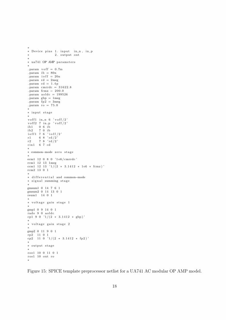
∗∗ Device p ins 1 . input in n , in p∗ 2 . output out∗∗ ua741 OP AMP parameters∗. param vo f f = 0 .7m. param ib = 80n. param i o f f = 20n. param rd = 2meg. param cd = 1 .4 p. param cmrrdc = 31622.8. param fcmz = 200 .0. param aoldc = 199526. param gbp = 1meg. param fp2 = 3meg. param ro = 75 .0∗∗ input s tage∗vo f f 1 in n 6 ’ v o f f /2 ’v o f f 2 7 in p ’ v o f f /2 ’ib1 0 6 ibib2 7 0 ibi o f f 1 7 6 ’ i o f f /2 ’r1 6 8 ’ rd /2 ’r2 7 8 ’ rd /2 ’c in1 6 7 cd∗∗ common−mode zero s tage∗ecm1 12 0 8 0 ’1 e6/cmrrdc ’rcm1 12 13 1megccm1 12 13 ’1/(2 ∗ 3 .1412 ∗ 1e6 ∗ fcmz ) ’rcm2 13 0 1∗∗ d i f f e r e n t i a l and common−mode∗ s i g n a l summing s tage∗gmsum1 0 14 7 6 1gmsum2 0 14 13 0 1rsum1 14 0 1∗∗ vo l tage gain s tage 1∗gmp1 0 9 14 0 1rado 9 0 ao ldccp1 9 0 ’1/(2 ∗ 3 .1412 ∗ gbp ) ’∗∗ vo l tage gain s tage 2∗gmp2 0 11 9 0 1rp2 11 0 1cp2 11 0 ’1/(2 ∗ 3 .1412 ∗ fp2 ) ’∗∗ output s tage∗eos1 10 0 11 0 1ros1 10 out ro∗
Figure 15: SPICE template preprocessor netlist for a UA741 AC modular OP AMP model.
18

. Def : s t o q f i g 1 7 net0 net1 net2Sub :X1 net0 net1 net2 gnd Type=”s t o q f i g 1 5 c i r ”. Def : End
. Def : s t o q f i g 1 5 c i r netIN N netOUT netIN P r e fR:ROS1 net10 netOUT R=”75”VCVS:EOS1 net11 net10 r e f r e f G=”1”C:CP2 net11 r e f C=”5.30583 e−08”R:RP2 net11 r e f R=”1”VCCS:GMP2 net9 r e f net11 r e f G=”1”C:CP1 net9 r e f C=”1.59175 e−07”R:RADO net9 r e f R=”199526”VCCS:GMP1 net14 r e f net9 r e f G=”1”R:RSUM1 net14 r e f R=”1”VCCS:GMSUM2 net13 r e f net14 r e f G=”1”VCCS:GMSUM1 net7 r e f net14 net6 G=”1”R:RCM2 net13 r e f R=”1”C:CCM1 net12 net13 C=”7.95874 e−10”R:RCM1 net12 net13 R=”1M”VCVS:ECM1 net8 net12 r e f r e f G=”31.6228”C: CIN1 net6 net7 C=”1.4 e−12”R:R2 net7 net8 R=”1e+06”R:R1 net6 net8 R=”1e+06”Idc : IOFF1 net7 net6 I=”1e−08”Idc : IB2 net7 r e f I=”8e−08”Idc : IB1 r e f net6 I=”8e−08”Vdc :VOFF2 net7 netIN P U=”0.00035”Vdc :VOFF1 netIN N net6 U=”0.00035”
. Def : End
Figure 16: Qucs netlist for a UA741 AC modular OP AMP model.
spice
IN_N OUT
IN_P
Ref
X1File=stoq_fig15.cir
P_IN_N
P_IN_P
P_OUT-+
SUB1
Figure 17: Qucs symbol for a UA741 AC modular OP AMP model.
19

-+
SUB1
V1U=1 V
C4C=0.175u
C3C=0.175u
C2C=0.45u
R6R=15k
R3R=22k
R4R=20k
R2R=100
R1R=100k
R5R=6.8k
C1C=2.2u
dc simulation
DC1
ac simulation
AC1Type=linStart=10 HzStop=101 HzPoints=200Equation
Eqn1gain_dB=dB(vout.v)phase_deg=phase(vout.v)
vout
vin
Figure 18: A twin-T notch filter circuit.
10 1005
10
15
acfrequency
vout
.v
10 100
16
18
20
22
24
acfrequency
gain
_dB
10 100
0
50
acfrequency
phas
e_de
g
Figure 19: Small signal transfer characteristics for a twin-T notch filter circuit.
20

Building circuit design equations into netlists
Figure 20 illustrates a bandpass filter that has a bandwidth which is small compared toit’s center frequency. The circuit is often referred to as the Dalyiannis-Friend filter afterits developers. The filter center frequency f0, voltage gain magnitude H0, bandwidth Band Q factor are given by the following equations:
• f0 =1
2πC√
(R1‖R2)R3
, where C = C1 = C2
• H0 =R3
2R1
• B =1
πR3C
• Q =f0
B=
1
2
√R3
R1‖R2
When designing a filter for a specific specification, for example say f0 = 1kHz, B = 200Hzand H0 = 10, values for the filter resistor and capacitor values need to be calculated. Thiscan, of course, be done manually. However, this process is often tedious, especially if anumber of filters need to be designed each with different specifications. Circuit simulatorsare by their very nature primarily designed to analyse and simulate the performance ofcircuits who’s component values are known. As such they are tools for analysis rather thandesign. In practice, of course, engineers employ circuit simulators to check their circuitdesigns. Qucs is attempting to bridge the gap between design and analysis by using add-on software components for designing circuits with well understood structures and designprocedures23.
23The Qucs Tools drop-down menu lists the currently available design functions that have been imple-mented with release of Qucs you are using.
OP1
R1
R3
C1
C2
R2
Vout
Vin
Figure 20: The Dalyiannis-Friend bandpass filter circuit.
21

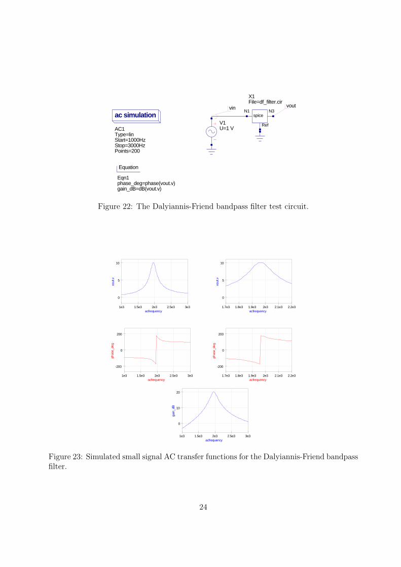
In the previous section it was shown that the SPICEPP preprocessor could be used tocalculate model component values. By a simple extension of this concept it is also possibleto embed design equations into a netlist. Shown in Fig. 21 is a SPICEPP netlist for theDalyiannis-Friend filter. The UA741 OP AMP is modelled with a SPICE subcircuit calledopamp_ac and has its own set of parameters24. The first set of design parameters representthe filter specification and are used in the SPICEPP conversion process to calculate thefilter resistor and capacitor component values. Note also the use of inline comments fordocumenting the netlist code. Figures. 22 and 23 show a basic filter test circuit and theresulting simulation transfer functions. Hence, not only can the SPICEPP preprocessorbe used for setting up device models but it can also aid the design of entire circuit blocksprovided design equations are available for a given circuit configuration. By combiningSPICEPP with Qucs a very significant design/analysis tool becomes available opening upnew possibilities for Qucs users.
24These are defined within a subcircuit and should have names unique to the subcircuit model beingdefined.
22

∗ Dely iann i s Friend Bandpass f i l t e r des ign∗ Design parameters. param f c = 2000.0 $ F i l t e r c en t e r f requency (Hz). param bw = 200.0 $ F i l t e r bandwidth (Hz). param q = 10 .0 $ F i l t e r q f a c t o r = f0 /bw. param r3 i v = 200k $ Assumed value f o r r f 3. param h0 = 10 .0 $ F i l t e r f 0 gain magnitude∗∗ F i l t e r c i r c u i t p ins : input n1 , output n3∗r3 n3 n4 r3 i vc1 n2 n3 ’ q /(3 .1412∗ f c ∗ r 3 i v ) ’c2 n2 n4 ’ q /(3 .1412∗ f c ∗ r 3 i v ) ’r1 n1 n2 ’ r 3 i v /(2∗h0 ) ’r2 n2 0 ’ r 3 i v /( (4∗q∗q)−(2∗h0 ) ) ’x1 0 n4 n3 opamp ac
∗ s u b c i r c u i t por t s : in+ in− out. subckt opamp ac in p in n out∗∗ ua741 OP AMP parameters. param vo f f = 0 .7m. param ib = 80n. param i o f f = 20n. param rd = 2meg. param cd = 1 .4 p. param cmrrdc = 31622.8. param fcmz = 200 .0. param aoldc = 199526. param gbp = 1meg. param fp2 = 3meg. param ro = 75 .0∗ input s tagevo f f 1 in n 6 ’ v o f f /2 ’v o f f 2 7 in p ’ v o f f /2 ’ib1 0 6 ibib2 7 0 ibi o f f 1 7 6 ’ i o f f /2 ’r1 6 8 ’ rd /2 ’r2 7 8 ’ rd /2 ’c in1 6 7 cd∗ common−mode zero s tageecm1 12 0 8 0 ’1 e6/cmrrdc ’rcm1 12 13 1megccm1 12 13 ’1/(2 ∗ 3 .1412 ∗ 1e6 ∗ fcmz ) ’rcm2 13 0 1∗ d i f f e r e n t i a l and common−mode s i g n a l summing s tagegmsum1 0 14 7 6 1gmsum2 0 14 13 0 1rsum1 14 0 1∗ vo l tage gain s tage 1gmp1 0 9 14 0 1rado 9 0 ao ldccp1 9 0 ’1/(2 ∗ 3 .1412 ∗ gbp ) ’∗ vo l tage gain s tage 2gmp2 0 11 9 0 1rp2 11 0 1cp2 11 0 ’1/(2 ∗ 3 .1412 ∗ fp2 ) ’∗∗ output s tageeos1 10 0 11 0 1ros1 10 out ro. ends
Figure 21: SPICEPP netlist for the Dalyiannis-Friend filter.
23
V1U=1 V
ac simulation
AC1Type=linStart=1000HzStop=3000HzPoints=200
spiceN1 N3
Ref
X1File=df_filter.cir
Equation
Eqn1phase_deg=phase(vout.v)gain_dB=dB(vout.v)
vin vout
Figure 22: The Dalyiannis-Friend bandpass filter test circuit.
1e3 1.5e3 2e3 2.5e3 3e3
0
5
10
acfrequency
vout
.v
1.7e3 1.8e3 1.9e3 2e3 2.1e3 2.2e3
0
5
10
acfrequency
vout
.v
1.7e3 1.8e3 1.9e3 2e3 2.1e3 2.2e3
-200
0
200
acfrequency
phas
e_de
g
1e3 1.5e3 2e3 2.5e3 3e3
-200
0
200
acfrequency
phas
e_de
g
1e3 1.5e3 2e3 2.5e3 3e3
0
10
20
acfrequency
gain
_dB
Figure 23: Simulated small signal AC transfer functions for the Dalyiannis-Friend bandpassfilter.
24

Global nodes
In the SPICE 2 and SPICE 3 hardware description languages only the earth node is global.By convention this is given node name 0 and is assumed by the SPICE language passerto be earth whenever it occurs in a circuit netlist. When connecting discreet componentswith other subcircuit blocks there is often a need for other nodes to be designated global;the classic example being power supply nodes. SPICEPP allows nodes to designated asglobal. These are effectively connected together to form one net covering both outsideand inside subcircuits. The best way to understand the use of global nodes is to consideran example. Figure 11 gives the SPICE netlist for the two section CMOS ring counter.Many readers would possibly have noticed that in this netlist both the NAND2 and NOR2subcircuits include internal voltage sources25. This is, of course, not necessary and indeedinefficient from a simulation point of view. A better approach would be to link individualgates with a power supply net. The SPICEPP netlist given in Fig. 24 illustrates how the.global command can be used to define a global power supply node. After passing this codethrough SPICEPP the SPICE netlist printed in Fig. 25 results. Simulation with Qucs givesthe same waveforms displayed in Fig. 13.
25The DC voltage supply for each logic block is generated by a pulse source. This has the effect ofsimulating the rising edge of the power supply switch on transient and aids DC convergence.
25

∗ Two stage CMOS r ing counter c i r c u i t .∗∗ External nodes : input 1 , output 4 , +ve supply nvcc∗∗ g l oba l node∗. g l oba l nvcc∗x1 1 5 6 nand2x2 1 6 7 nand2x3 3 6 2 nand2x4 2 7 3 nand2x5 1 2 8 nor2x6 1 8 9 nor2x7 5 8 4 nor2x8 4 9 5 nor2∗. model modp pmos( vto=−1 kp=10u+ cgdo=0.2n cgso =0.2n cgbo=2n). model modn nmos( vto=1 kp=10u+ cgdo=0.2n cgso =0.2n cgbo=2n)∗. subckt nand2 1 2 3m1 3 1 nvcc nvcc modp w=40u l=5um2 3 2 nvcc nvcc modp w=40u l=5um3 5 1 0 0 modn w=20u l=5um4 3 2 5 5 modn w=20u l=5uc1 1 0 10pc2 2 0 10p∗vcc 4 0 pu l s e ( 0 5 0 1ns 1ns 1 2). ends∗. subckt nor2 1 2 3m1 4 1 nvcc nvcc modp w=40u l=5um2 3 2 4 4 modp w=40u l=5um3 3 2 0 0 modn w=20u l=5um4 3 1 0 0 modn w=20u l=5uc1 1 0 10pc2 2 0 10p∗vcc 7 0 pu l s e ( 0 5 0 1ns 1ns 1 2). ends
Figure 24: SPICEPP netlist for a two section CMOS ring counter with global power supplynet node nvcc.
26

∗ Two stage CMOS r ing counter c i r c u i t .x1 1 5 6 nvcc nand2x2 1 6 7 nvcc nand2x3 3 6 2 nvcc nand2x4 2 7 3 nvcc nand2x5 1 2 8 nvcc nor2x6 1 8 9 nvcc nor2x7 5 8 4 nvcc nor2x8 4 9 5 nvcc nor2. model modp pmos vto=−1 kp=10u cgdo=0.2n cgso =0.2n cgbo=2n. model modn nmos vto=1 kp=10u cgdo=0.2n cgso =0.2n cgbo=2n. subckt nand2 1 2 3 nvccm1 3 1 nvcc nvcc modp w=40u l=5um2 3 2 nvcc nvcc modp w=40u l=5um3 5 1 0 0 modn w=20u l=5um4 3 2 5 5 modn w=20u l=5uc1 1 0 10pc2 2 0 10p. ends. subckt nor2 1 2 3 nvccm1 4 1 nvcc nvcc modp w=40u l=5um2 3 2 4 4 modp w=40u l=5um3 3 2 0 0 modn w=20u l=5um4 3 1 0 0 modn w=20u l=5uc1 1 0 10pc2 2 0 10p. ends
Figure 25: SPICE netlist for a two section CMOS ring counter with global power supplynet node nvcc.
End Note
This tutorial note describes how SPICE netlists can be simulated using Qucs. The textis much more than a basic outline of the processes needed to link SPICE circuit files toQucs. While writing this note an attempt has been made to stress the fact that topics likeSPICE/Qucs netlist compatibility and conversion are important to the future developmentof Qucs. So an interesting, and thought provoking question, is how does Qucs develop nextin relation to SPICE and indeed how best is it to make sure that Qucs users can get themost from all the published SPICE information and device models? After all there is nopoint in reinventing the wheel! Complete compatibility with SPICE will not be possibleuntil all the basic SPICE 2 and SPICE 3 primitive components are added to Qucs. This willtake time but is happening as the Qucs team develops the package26. Adding equationsto component calculations is a very much a current active topic in Qucs development.Recently, Michael Magraf has added parameter passing to the Qucs GUI. Stefan Jahn willadd the necessary simulator routines for handling equations and parameter passing whentime allows. In the long term not only will it be possible to determine component valuesusing calculations at the simulation initialisation phase but it will also be possible to allowsuch components to be dependent on simulation voltage and current variables. Qucs will
26Michael Magraf has recently added a four terminal transmission line to Qucs. Future testing willconfirm if this is similar to the SPICE T component.
27

then be able to simulate circuits containing nonlinear voltage and current sources like theSPICE 3 B component. These notes are very much a report on some of the work on Qucsdevice modelling I have been doing in recent months. Again if there is enough interest inthis area of Qucs development I will upgrade them in the future. My thanks to StefanJahn for all his encouragement while I have been developing the material reported in thistutorial note.
28