Quarch Technology Ltd Torridon PCIe x16 Gen 3 Control ... - PCIe x16 Gen 3... · Quarch Technology...
31
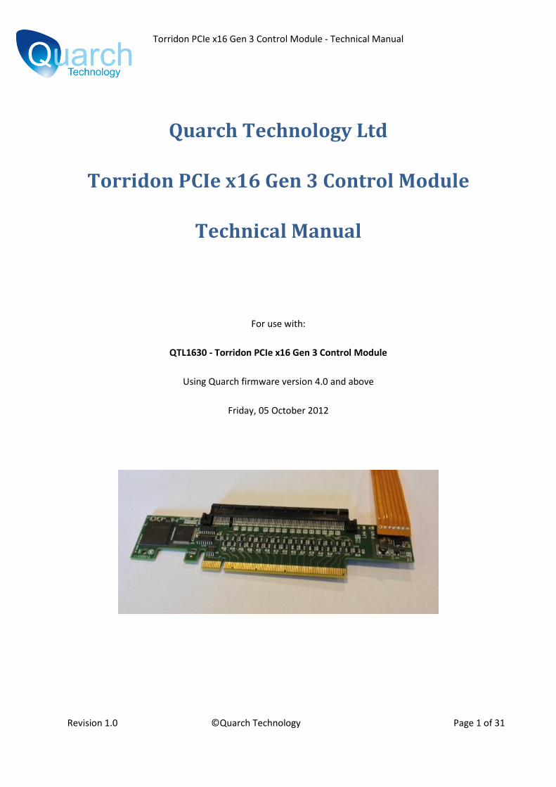
Torridon PCIe x16 Gen 3 Control Module - Technical Manual Revision 1.0 ©Quarch Technology Page 1 of 31 Quarch Technology Ltd Torridon PCIe x16 Gen 3 Control Module Technical Manual For use with: QTL1630 - Torridon PCIe x16 Gen 3 Control Module Using Quarch firmware version 4.0 and above Friday, 05 October 2012
Transcript of Quarch Technology Ltd Torridon PCIe x16 Gen 3 Control ... - PCIe x16 Gen 3... · Quarch Technology...
Torridon PCIe x16 Gen 3 Control Module - Technical Manual
Revision 1.0 ©Quarch Technology Page 1 of 31
Quarch Technology Ltd
Torridon PCIe x16 Gen 3 Control Module
Technical Manual
For use with:
QTL1630 - Torridon PCIe x16 Gen 3 Control Module
Using Quarch firmware version 4.0 and above
Friday, 05 October 2012

Torridon PCIe x16 Gen 3 Control Module - Technical Manual
Revision 1.0 ©Quarch Technology Page 2 of 31
Change History
1.0 4th October 2012 Pre-Release Version – subject to change
Torridon PCIe x16 Gen 3 Control Module - Technical Manual
Revision 1.0 ©Quarch Technology Page 3 of 31
Contents Introduction ..........................................................................................................................4
Technical Specifications .........................................................................................................5
Switching Characteristics: ................................................................................................................... 5
High Speed Switch Characteristics ...................................................................................... 5
Mechanical Characteristics: ....................................................................................................7
QTL1630 PCIe x16 Gen 3 Control module ........................................................................... 7
LEDs 8
Control Interfaces ..................................................................................................................8
Basic Concepts .......................................................................................................................9
Signal Configuration.......................................................................................................................... 10
Power Up vs. Power Down Timing ................................................................................................... 12
Pin Bounce Modes ............................................................................................................................ 13
Glitch Control .................................................................................................................................... 15
Voltage Measurements .................................................................................................................... 18
Default Startup State ........................................................................................................................ 19
Controlling the Module ........................................................................................................ 21
Serial Command Set.......................................................................................................................... 21
SCPI Style Commands ........................................................................................................ 21
Control Register Map ........................................................................................................... 29
Appendix 1 - Signal Names ................................................................................................... 30

Torridon PCIe x16 Gen 3 Control Module - Technical Manual
Revision 1.0 ©Quarch Technology Page 4 of 31
Introduction
The Torridon PCIe x16 Gen 3 Control module allows remote switching of PCIe data, power and
supporting control pins in a PCIe x16 Gen 3 slot for test automation or fault injection purposes.
The module supports PCIe Gen 2 and Gen 3 devices at data rates up to 8 GT/s.
Each pin is individually switched, allowing complete control over the mating of the card connector.
Any individual pin(s) can be disconnected or glitched to simulate failures or configuration changes. If
the devices support hot-swap, a sequenced hot-swap event can be run, connecting pins in sequence
and simulating pin-bounce if required.
WARNING: Many systems DO NOT support hot-swap of a PCIe card while the system is powered up.
You should only use this feature if you are certain it should not damage your hardware.
The module can disrupt power, data and control signals down to a minimum glitch length of 50nS.
(*The practical minimum time for some pins, such as power pins, may be longer than this)
Torridon PCIe x16 Gen 3 Control Module - Technical Manual
Revision 1.0 ©Quarch Technology Page 5 of 31
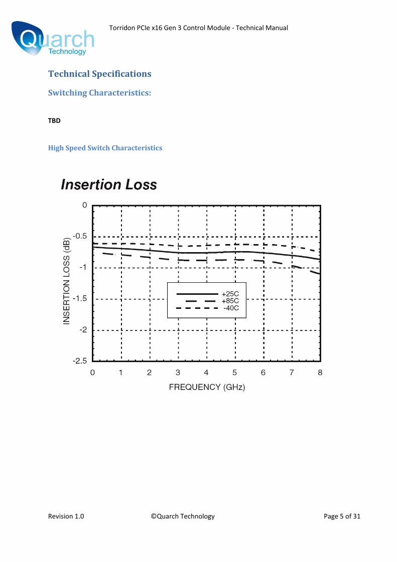
Technical Specifications
Switching Characteristics:
TBD
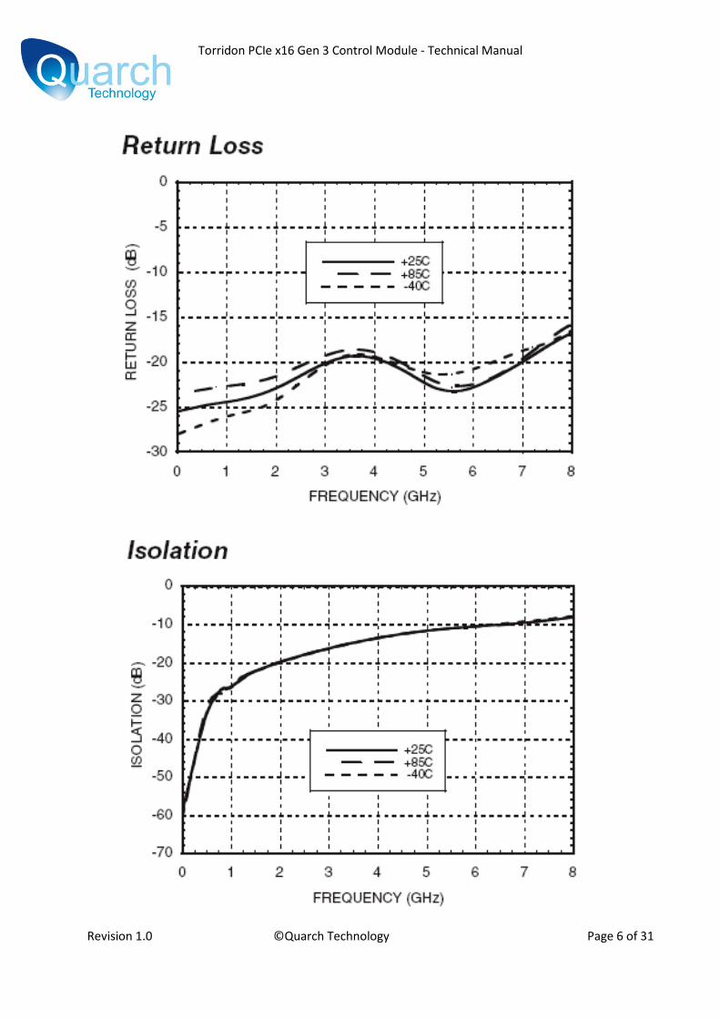
High Speed Switch Characteristics
Torridon PCIe x16 Gen 3 Control Module - Technical Manual
Revision 1.0 ©Quarch Technology Page 6 of 31

Torridon PCIe x16 Gen 3 Control Module - Technical Manual
Revision 1.0 ©Quarch Technology Page 7 of 31
Mechanical Characteristics:
QTL1630 PCIe x16 Gen 3 Control module
TBD
Torridon PCIe x16 Gen 3 Control Module - Technical Manual
Revision 1.0 ©Quarch Technology Page 8 of 31
LEDs
The module has 2 LEDs:
PWR: This LED is green when the module is supplied with external power through its ribbon cable.
LINK: This LED is shows the connection state of the attached PCIe card. This LED has 3 states:
OFF: ALL PCIe pins are disconnected
GREEN: ALL PCIe pins are connected
ORANGE: Some, but not all, PCIe pins are connected
Control Interfaces
All Torridon Control Modules are designed to be used with a Torridon Array Controller (QTL1079) or
a single Torridon Interface Card (QTL1144).
The control cable is an ultra-thin Flex cable.
Control Interface Form Factor Torridon
Module Ports
Control Methods
Available
Interfaces
Torridon Array
Controller
1U 19” Rack
Mounted unit
24 at the front, 4
at the rear
Serial Scripting
Script Generation
through TestMonkey
GUI
Serial via DB9 or
RJ45
Ethernet
Torridon Interface
Card
102mm x
26mm PCB
1 port Serial Scripting
Script Generation
through TestMonkey
GUI
Real-time USB
Control via
TestMonkey GUI
Serial via DB9 or
RJ45
USB
Torridon PCIe x16 Gen 3 Control Module - Technical Manual
Revision 1.0 ©Quarch Technology Page 9 of 31
Basic Concepts
Each switch on the module is called a ‘Signal’ and can be programmed to follow one of 6
programmable delay and bounce profiles (called ‘Sources’). This allows the user to sequence the
signal connections in the cable in up to six programmable steps.
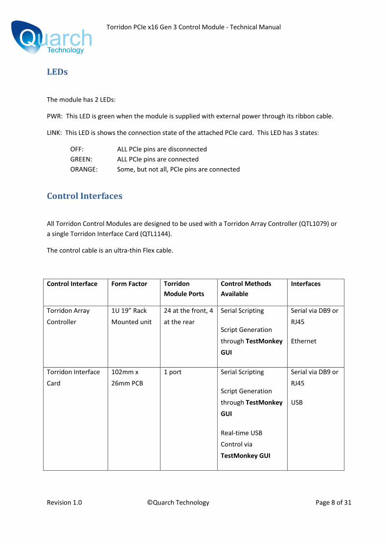
Each of the programmable delay and bounce profiles is called a control source, S1 to S6. For each
control source the user sets up a delay, and bounce parameters. Three special sources (S0, S7 and
S8) are also provided as described in the table below.
Control Source Parameters for a power up event (Basic Pin Bounce):
Once each delay period is set up, the user assigns each signal to follow the relevant control source,
then uses the “run:power up” and “run:power down” commands to initiate the hot-swap.
The BUSY bit 1 in the control register is set during a power up, power down and short operation.
This may be used to monitor for the completion of timed events.
DELAY
BOUNCE
PERIOD
HOT_SWAP
BOUNCE LENGTH
BOUNCE DUTY
CYCLE
Torridon PCIe x16 Gen 3 Control Module - Technical Manual
Revision 1.0 ©Quarch Technology Page 10 of 31
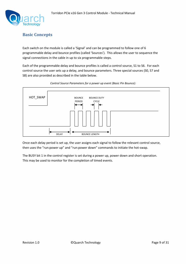
Power up and Power down example:
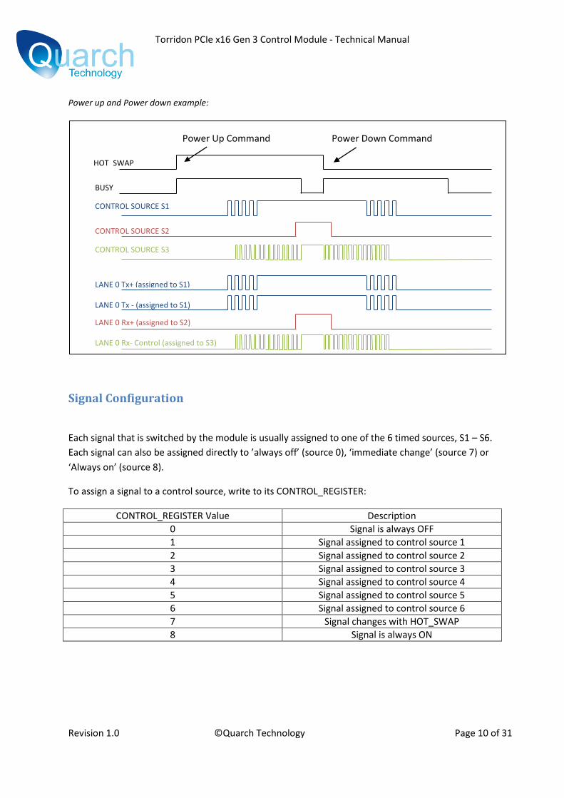
Signal Configuration
Each signal that is switched by the module is usually assigned to one of the 6 timed sources, S1 – S6.
Each signal can also be assigned directly to ’always off’ (source 0), ‘immediate change’ (source 7) or
‘Always on’ (source 8).
To assign a signal to a control source, write to its CONTROL_REGISTER:
CONTROL_REGISTER Value Description
0 Signal is always OFF
1 Signal assigned to control source 1
2 Signal assigned to control source 2
3 Signal assigned to control source 3
4 Signal assigned to control source 4
5 Signal assigned to control source 5
6 Signal assigned to control source 6
7 Signal changes with HOT_SWAP
8 Signal is always ON
HOT_SWAP
CONTROL SOURCE S1
CONTROL SOURCE S2
CONTROL SOURCE S3
BUSY
LANE 0 Tx+ (assigned to S1)
LANE 0 Tx - (assigned to S1)
LANE 0 Rx+ (assigned to S2)
LANE 0 Rx- Control (assigned to S3)
Power Up Command Power Down Command
Torridon PCIe x16 Gen 3 Control Module - Technical Manual
Revision 1.0 ©Quarch Technology Page 11 of 31
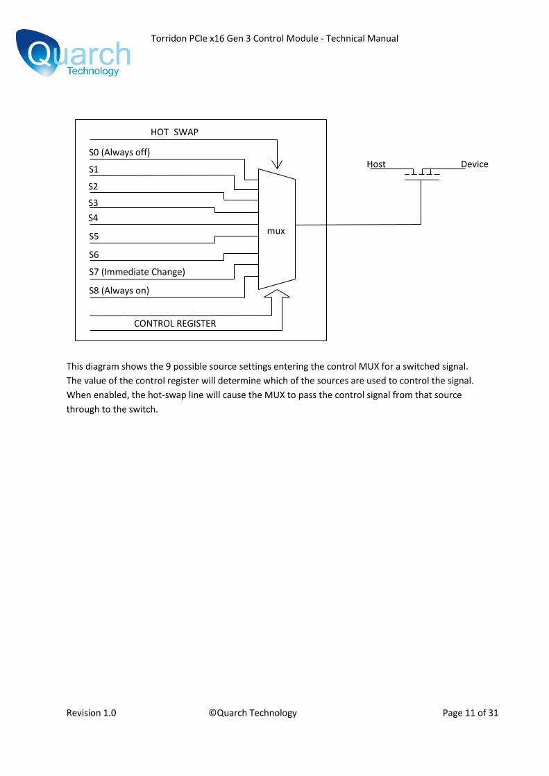
This diagram shows the 9 possible source settings entering the control MUX for a switched signal.
The value of the control register will determine which of the sources are used to control the signal.
When enabled, the hot-swap line will cause the MUX to pass the control signal from that source
through to the switch.
HOT_SWAP
S2
S3
S4
S5
S6
S7 (Immediate Change)
S0 (Always off)
S1
CONTROL REGISTER
Host
mux
S8 (Always on)
Device
Torridon PCIe x16 Gen 3 Control Module - Technical Manual
Revision 1.0 ©Quarch Technology Page 12 of 31
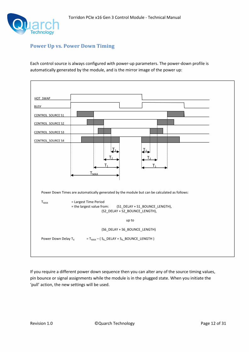
Power Up vs. Power Down Timing
Each control source is always configured with power-up parameters. The power-down profile is
automatically generated by the module, and is the mirror image of the power up:
If you require a different power down sequence then you can alter any of the source timing values,
pin bounce or signal assignments while the module is in the plugged state. When you initiate the
‘pull’ action, the new settings will be used.
BUSY
CONTROL SOURCE S1
CONTROL_SOURCE S2
CONTROL_SOURCE S3
CONTROL_SOURCE S4
HOT_SWAP
T1
T2
T3
T1
T2
T3
Power Down Times are automatically generated by the module but can be calculated as follows:
TMAX = Largest Time Period = the largest value from: (S1_DELAY + S1_BOUNCE_LENGTH), (S2_DELAY + S2_BOUNCE_LENGTH), up to (S6_DELAY + S6_BOUNCE_LENGTH) Power Down Delay TX = TMAX – ( SX_DELAY + SX_BOUNCE_LENGTH )
TMAX
Torridon PCIe x16 Gen 3 Control Module - Technical Manual
Revision 1.0 ©Quarch Technology Page 13 of 31
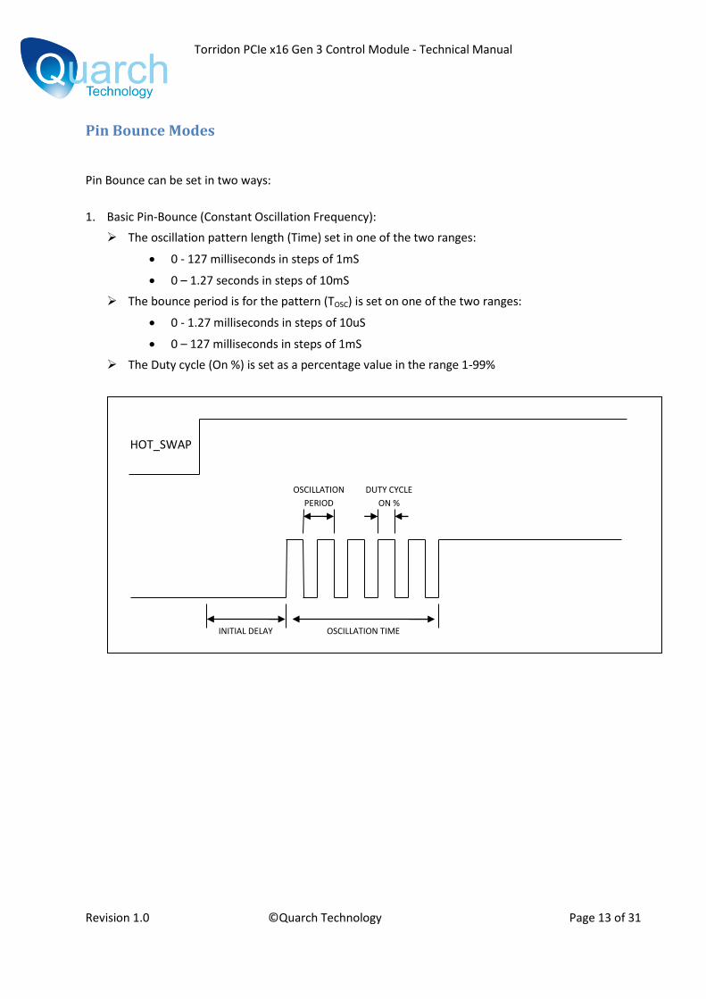
Pin Bounce Modes
Pin Bounce can be set in two ways:
1. Basic Pin-Bounce (Constant Oscillation Frequency):
The oscillation pattern length (Time) set in one of the two ranges:
0 - 127 milliseconds in steps of 1mS
0 – 1.27 seconds in steps of 10mS
The bounce period is for the pattern (TOSC) is set on one of the two ranges:
0 - 1.27 milliseconds in steps of 10uS
0 – 127 milliseconds in steps of 1mS
The Duty cycle (On %) is set as a percentage value in the range 1-99%
INITIAL DELAY
OSCILLATION
PERIOD
HOT_SWAP
OSCILLATION TIME
DUTY CYCLE
ON %
Torridon PCIe x16 Gen 3 Control Module - Technical Manual
Revision 1.0 ©Quarch Technology Page 14 of 31
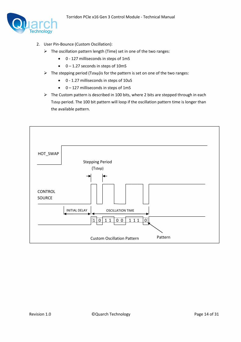
2. User Pin-Bounce (Custom Oscillation):
The oscillation pattern length (Time) set in one of the two ranges:
0 - 127 milliseconds in steps of 1mS
0 – 1.27 seconds in steps of 10mS
The stepping period (Tstep)is for the pattern is set on one of the two ranges:
0 - 1.27 milliseconds in steps of 10uS
0 – 127 milliseconds in steps of 1mS
The Custom pattern is described in 100 bits, where 2 bits are stepped through in each
Tstep period. The 100 bit pattern will loop if the oscillation pattern time is longer than
the available pattern.
INITIAL DELAY
Stepping Period
(Tstep)
Custom Oscillation Pattern
1 0 1 1 1 1 1 0 0 0
HOT_SWAP
CONTROL
SOURCE
Pattern
OSCILLATION TIME
Torridon PCIe x16 Gen 3 Control Module - Technical Manual
Revision 1.0 ©Quarch Technology Page 15 of 31
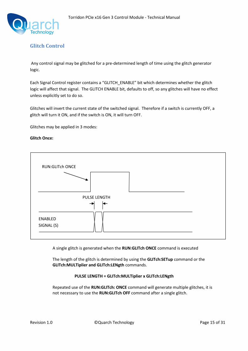
Glitch Control
Any control signal may be glitched for a pre-determined length of time using the glitch generator
logic.
Each Signal Control register contains a “GLITCH_ENABLE” bit which determines whether the glitch
logic will affect that signal. The GLITCH ENABLE bit, defaults to off, so any glitches will have no effect
unless explicitly set to do so.
Glitches will invert the current state of the switched signal. Therefore if a switch is currently OFF, a
glitch will turn it ON, and if the switch is ON, it will turn OFF.
Glitches may be applied in 3 modes: Glitch Once:
A single glitch is generated when the RUN:GLITch ONCE command is executed The length of the glitch is determined by using the GLITch:SETup command or the GLITch:MULTiplier and GLITch:LENgth commands.
PULSE LENGTH = GLITch:MULTiplier x GLITch:LENgth
Repeated use of the RUN:GLITch: ONCE command will generate multiple glitches, it is not necessary to use the RUN:GLITch OFF command after a single glitch.
PULSE LENGTH
RUN:GLITch ONCE
ENABLED
SIGNAL (S)
Torridon PCIe x16 Gen 3 Control Module - Technical Manual
Revision 1.0 ©Quarch Technology Page 16 of 31
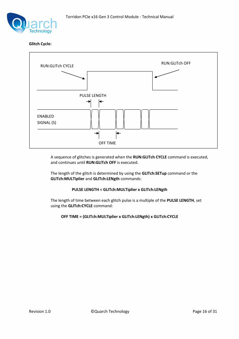
Glitch Cycle:
A sequence of glitches is generated when the RUN:GLITch CYCLE command is executed, and continues until RUN:GLITch OFF is executed. The length of the glitch is determined by using the GLITch:SETup command or the GLITch:MULTiplier and GLITch:LENgth commands:
PULSE LENGTH = GLITch:MULTiplier x GLITch:LENgth The length of time between each glitch pulse is a multiple of the PULSE LENGTH, set using the GLITch:CYCLE command:
OFF TIME = (GLITch:MULTiplier x GLITch:LENgth) x GLITch:CYCLE
PULSE LENGTH
RUN:GLITch CYCLE
ENABLED
SIGNAL (S)
RUN:GLITch OFF
OFF TIME
Torridon PCIe x16 Gen 3 Control Module - Technical Manual
Revision 1.0 ©Quarch Technology Page 17 of 31
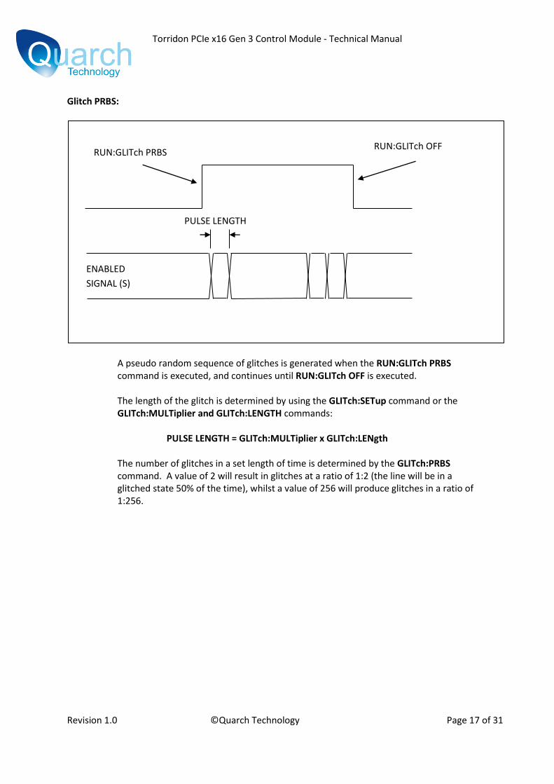
Glitch PRBS:
A pseudo random sequence of glitches is generated when the RUN:GLITch PRBS command is executed, and continues until RUN:GLITch OFF is executed. The length of the glitch is determined by using the GLITch:SETup command or the GLITch:MULTiplier and GLITch:LENGTH commands:
PULSE LENGTH = GLITch:MULTiplier x GLITch:LENgth
The number of glitches in a set length of time is determined by the GLITch:PRBS command. A value of 2 will result in glitches at a ratio of 1:2 (the line will be in a glitched state 50% of the time), whilst a value of 256 will produce glitches in a ratio of 1:256.
PULSE LENGTH
RUN:GLITch PRBS
ENABLED
SIGNAL (S)
RUN:GLITch OFF

Torridon PCIe x16 Gen 3 Control Module - Technical Manual
Revision 1.0 ©Quarch Technology Page 18 of 31
Voltage Measurements
The modules are capable of measuring various voltages both for self. The following measurement
points are available:
Measurement Command Description Resolution / Accuracy
MEASure:VOLTage:SELF 1v2? Returns the voltage of the
modules internal 1.2v power
rail
64mV / 5%
MEASure:VOLTage:SELF 3v3? Returns the voltage of the
modules internal 3.3v power
rail – This powers the modules
internal circuitry, and the active
circuitry on the IN connector
64mV / 5%
MEASure:VOLTage:SELF 12v? Returns the voltage of the
modules internal 12v power
rail
64mV/ 5%
Torridon PCIe x16 Gen 3 Control Module - Technical Manual
Revision 1.0 ©Quarch Technology Page 19 of 31
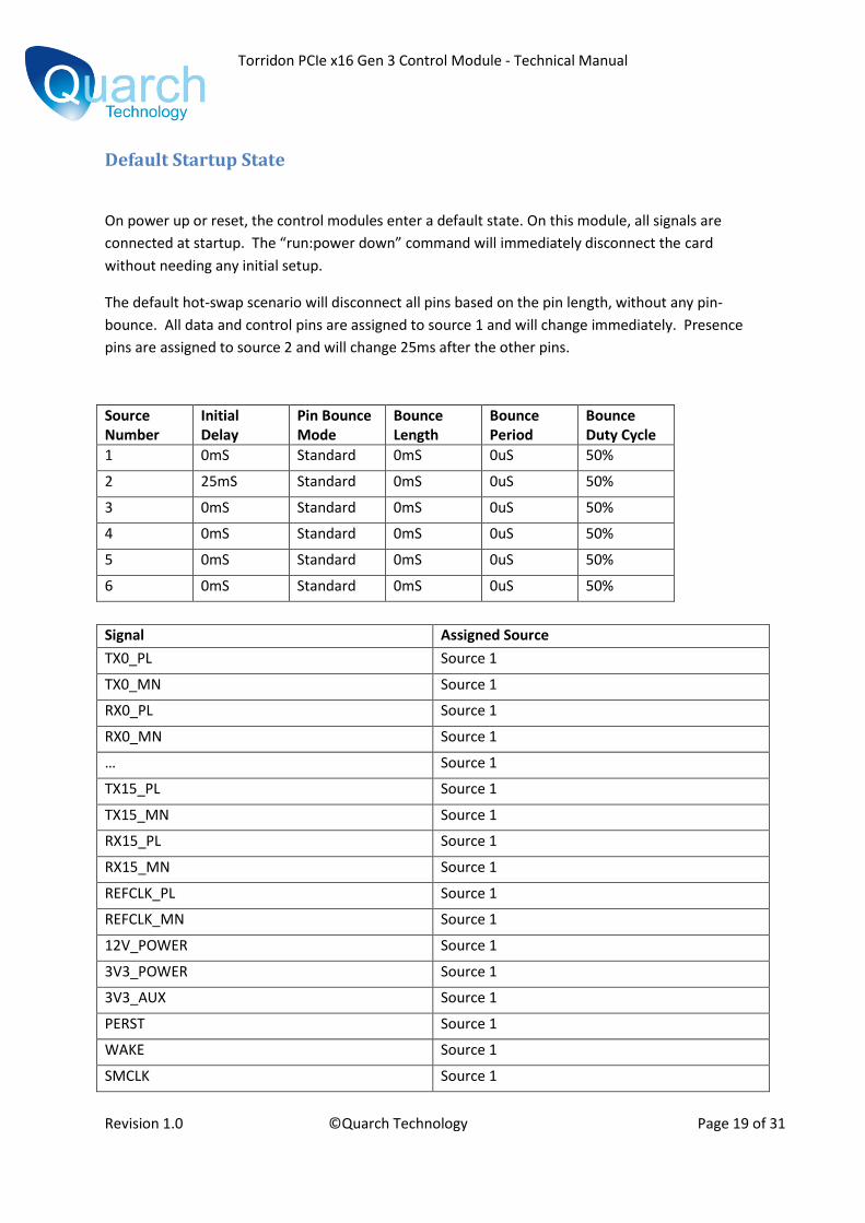
Default Startup State
On power up or reset, the control modules enter a default state. On this module, all signals are
connected at startup. The “run:power down” command will immediately disconnect the card
without needing any initial setup.
The default hot-swap scenario will disconnect all pins based on the pin length, without any pin-
bounce. All data and control pins are assigned to source 1 and will change immediately. Presence
pins are assigned to source 2 and will change 25ms after the other pins.
Source Number
Initial Delay
Pin Bounce Mode
Bounce Length
Bounce Period
Bounce Duty Cycle
1 0mS Standard 0mS 0uS 50%
2 25mS Standard 0mS 0uS 50%
3 0mS Standard 0mS 0uS 50%
4 0mS Standard 0mS 0uS 50%
5 0mS Standard 0mS 0uS 50%
6 0mS Standard 0mS 0uS 50%
Signal Assigned Source
TX0_PL Source 1
TX0_MN Source 1
RX0_PL Source 1
RX0_MN Source 1
… Source 1
TX15_PL Source 1
TX15_MN Source 1
RX15_PL Source 1
RX15_MN Source 1
REFCLK_PL Source 1
REFCLK_MN Source 1
12V_POWER Source 1
3V3_POWER Source 1
3V3_AUX Source 1
PERST Source 1
WAKE Source 1
SMCLK Source 1
Torridon PCIe x16 Gen 3 Control Module - Technical Manual
Revision 1.0 ©Quarch Technology Page 20 of 31
SMDAT Source 1
PRESENT1 Source 2
PRESENT2_B17 Source 2
PRESENT2_B31 Source 2
PRESENT2_B48 Source 2
PRESENT2_B81 Source 2
TRST Source 1
TCK Source 1
TDO Source 1
TDI Source 1
TMS Source 1
Hot-Swap State:
The module is in the ‘plugged’ state, waiting for a RUN:POWer DOWN command to disconnect it.

Torridon PCIe x16 Gen 3 Control Module - Technical Manual
Revision 1.0 ©Quarch Technology Page 21 of 31
Controlling the Module
The module can be controlled either by:
Serial ASCII terminal (such as HyperTerminal)
This is normally used with scripted commands to automate a series of tests. The commands
are normally generated by a script or user code (PERL, TCL, C, C# or similar).
Telnet Terminal (Only when connected to an Array Controller). This mode uses exactly the
same commands as the serial ASCII terminal
USB
Quarch’s TestMonkey application can control a single module via USB, this allows simple
graphical control of the module.
Serial Command Set
When connected via a serial terminal, the module has a simple command line interface
SCPI Style Commands
These commands are based on the SCPI style control system that is used by many manufacturers of
test instruments. The entire SCPI specification has NOT been implemented but the command
structure will be very familiar to anyone who has used it before.
SCPI commands are NOT case sensitive
SCPI commands are in a hierarchy separated by ‘:’ (LEVel1:LEVel2:LEVel3)
Most words have a short form (e.g. ‘register’ shortens to ‘reg’). This will be documented as
REGister, where the short form is shown in capitals.
Some commands take parameters. These are separated by spaces after the main part of the
command (e.g. “meas:volt:self 3v3?” Obtains the 3v3 self test measurement)
Query commands that return a value all have a ‘?’ on the end
Commands with a preceding ‘*’ are basic control commands, found on all devices
Commands that do not return a particular value will return “OK” or “FAIL”. Unless disabled,
the fail response will also append a text description for the failure if it can be determined.
# [comments]
Any line beginning with a # character is ignored as a comment. This allows commenting of
scripts for use with the module.
Torridon PCIe x16 Gen 3 Control Module - Technical Manual
Revision 1.0 ©Quarch Technology Page 22 of 31
*RST
Triggers a reset, the module will behave as if it had just been powered on
*CLR
Clear the terminal window and displays the normal start screen. Also runs the internal self test.
The same action can be performed by pressing return on a blank line.
*IDN?
Displays a standard set of information, identifying the device. An example return is shown below
Family: Torridon System [The parent family of the device]
Name: Ethernet Cable Pull Module [The name of the device]
Part#: QTL1271-01 [The part number of the hardware]
Processor: QTL1159-01,3.50 [Part# and version of firmware]
Bootloader: QTL1170-01,1.00 [Part# and version of bootloader]
FPGA 1: 1.0 [Version of FPGA core]
*TST? Runs a set of standard tests to confirm the device is operating correctly, these tests are also
performed at start up. Returns ‘OK’ or ‘FAIL’ followed by a list of errors that occurred, each on a
new line.
CONFig:MODE BOOT Configures the card for boot loader mode (to update the firmware), requires an update utility on
the PC.
CONFig:MESSages [SHORt|USER]
CONFig:MESSages?
Gets or sets the mode for messages that are returned to the user’s terminal
Short: Only a “FAIL” or “OK” will be returned
User: Full error messages are returned to the user on failure
CONFig:TERMinal USER
Sets the terminal response mode to the default ‘User’ setting. This is intended for use with
HyperTerminal or similar and manually typed commands

Torridon PCIe x16 Gen 3 Control Module - Technical Manual
Revision 1.0 ©Quarch Technology Page 23 of 31
CONFig:TERMinal SCRIPT
Sets the terminal response mode for easier parsing. Especially useful from a UNIX/LINUX based
system. Characters sent from the PC are not echoed by the device and a <CR><LF> is sent after
the cursor to force a flush of the USART buffer.
CONFig:TERMinal ? Returns the current terminal mode
CONFig:DEFault:STATE
Resets the state of the module. This will set all source/signal/glitch etc logic to its default
power-on values. Terminal setting will not be affected. This command allows the module to
be brought back to a known state without resetting it.
DEPRECATED COMMANDS – Provided for backwards compatibility, we strongly suggest you use the
‘Signal’ and ‘Source’ commands instead.
REGister:READ [0xAA]
Returns the value of the register with address [0xAA]. [0xAA] should be in hex format and
preceded by the suffix “0x”. e.g. “0x6D”. The value is returned in the same form as the
address.
REGister:DUMP [0xA1] [0xA2]
Returns the value of each register in a range, starting at the first register address, up to the
second. [0xA1] and [0xA2] should be in hex format and preceded by the suffix “0x”. Each
data value will be returned on a new line.
REGister:WRITe [0xAA] [0xDD]
Writes the byte [0xDD] to register [0xAA], both [0xDD] and [0xAA] should be in hex format
and preceded by the suffix “0x”. The command returns “OK” or “FAIL”.

Torridon PCIe x16 Gen 3 Control Module - Technical Manual
Revision 1.0 ©Quarch Technology Page 24 of 31
SOURce:[1-6|ALL]:SETup [#1] [#2] [#3] [#4]
Sets up the source in a single command. All parameters are positive integer numbers:
#1 = Initial delay (mS)
[Limits: 0 to 127ms in steps of 1ms, 0 to 1270ms in steps of 10ms]
#2 = Bounce length (mS)
[Limits: 0 to 127ms in steps of 1ms, 0 to 1270ms in steps of 10ms]
#3 = Bounce Period (uS)
[Limits: 10 to 1270us in steps of 10us, 1000 to 127000us in steps of 1000us]
#4 = Duty Cycle (%)
[Limits: 0 to 100% in steps of 1%]
SOURce:[1-6|ALL]:DELAY [#ms]
SOURce:[1-6|ALL]:DELAY?
Sets the initial delay of a source in mS. The delay is entered as a integer number with no
units. E.g. “Source:1:delay 300”.
#1 = Initial delay (mS)
[Limits: 0 to 127ms in steps of 1ms, 0 to 1270ms in steps of 10ms]
SOURce:[1-6|ALL]:BOUNce:SETup [#1] [#2] [#3]
Sets up the bounce parameters in a single command. All parameters are positive integer
numbers:
#1 = Bounce length (mS)
[Limits: 0 to 127ms in steps of 1ms, 0 to 1270ms in steps of 10ms]
#2 = Bounce Period (uS)
[Limits: 10 to 1270us in steps of 10us, 1000 to 127000us in steps of 1000us]
#3 = Duty Cycle (%)
[Limits: 0 to 100% in steps of 1%]
SOURce:[1-6|ALL]:BOUNce:LENgth [#ms]
SOURce:[1-6|ALL]:BOUNce:LENgth?
Sets the length of the pin bounce in mS. The delay is entered as a decimal number with
no units. E.g. “Sour:2:boun:len 50”.
#1 = Bounce length (mS)
[Limits: 0 to 127ms in steps of 1ms, 0 to 1270ms in steps of 10ms]

Torridon PCIe x16 Gen 3 Control Module - Technical Manual
Revision 1.0 ©Quarch Technology Page 25 of 31
SOURce:[1-6|ALL]:BOUNce:PERiod [#us]
SOURce:[1-6|ALL]:BOUNce:PERiod?
Sets the bounce period of the pin bounce in uS. The value is entered as a decimal
number with no units. E.g. “Sour:6:boun:period 300”.
#1 = Bounce Period (uS)
[Limits: 10 to 1270us in steps of 10us, 1000 to 127000us in steps of 1000us]
SOURce:[1-6|ALL]:BOUNce:DUTY [#%]
SOURce:[1-6|ALL]:BOUNce:DUTY?
Sets the duty cycle of the pin bounce as a %. The value is entered as a decimal number
with no units. E.g. “source:3:bounce:duty 50”.
#1 = Duty Cycle (%)
[Limits: 0 to 100% in steps of 1%]
SOURce:[1-6|ALL]:BOUNce:MODE [SIMPLE|USER]
SOURce:[1-6|ALL]:BOUNce:MODE?
Sets the bounce pattern to SIMPLE (Duty cycle driven oscillation) or USER (User defined
custom pattern).
SOURce:[1-6|ALL]:BOUNce:PATtern:WRITe [0xAAAA] [0xDDDD]
Writes a word of the custom bounce pattern to the give address within the pattern
0xAAAA is the address (for example 0x0002)
0xDDDD is the pattern data (for example 0x13F2)
SOURce:[1-6|ALL]:BOUNce:PATtern:READ [0xAAAA]
Reads a word of the custom bounce pattern
0xAAAA is the address (for example 0x0002)
SOURce:[1-6|ALL]:BOUNce:PATtern:DUMP [0xAAAA] [0xAAAA]
Reads a range of words from the custom bounce pattern
0xAAAA is the start and end address range (for example 0x0002)
Torridon PCIe x16 Gen 3 Control Module - Technical Manual
Revision 1.0 ©Quarch Technology Page 26 of 31
SOURce:[1-6|ALL]:BOUNce:CLEAR
Removes any pin bounce from the source and sets all bounce settings to default values. See “Default Startup State” for details for the default settings.
SOURce:[1-6|ALL]:STATE [ON|OFF]
SOURce:[1-6|ALL]:STATE?
Sets or returns the enable state of the source. Any signals assigned to a disabled (off)
source will immediately be disconnected and vice versa. If a source state is changed, all
signals assigned to it will change at exactly the same time (if a change is required).
SIGnal:[SIG_NAME|ALL]:SETup [#num]
SIGnal:[SIG_NAME|ALL]:SOURce [#num]
Assigns a given signal to a numbered timing source (0-8). SIGNAL_NAME is one of the signals/groups as found in the ‘Signal Names’ appendix at the end of this manual
SIGnal:[SIG_NAME|ALL]:GLITch:ENAble [ON|OFF] SIGnal:[SIG_NAME|ALL]:GLITch:ENAble?
Enables a signal for glitching. If this in on, the signal will be glitched whenever the glitch logic is in use. Multiple signals may be set to glitch at the same time.
GLITch:SETup [MULTIPLIER_STEP] [#count] Sets up the glitch of the glitch in a single command. #1 = Multiplier factor for glitch length (mS)
[50ns|500sn|5us|50us|500us|5ms|50ms|500ms]
#2 = Length of the glitch (number of times the multiplication factor will be run)
[Limits: 0 to 31 in steps of 1]
This gives a maximum glitch of 15.5 Seconds. GLITch:MULTiplier [MULTIPILER_STEP] GLITch:MULTiplier?
Sets the multiplier value for the glitch time to one of the specified durations. This factor is multiplied with the GLITch:LENgth value to give the actual glitch time. #1 = Multiplier factor for glitch length (mS)
[50ns|500sn|5us|50us|500us|5ms|50ms|500ms]

Torridon PCIe x16 Gen 3 Control Module - Technical Manual
Revision 1.0 ©Quarch Technology Page 27 of 31
GLITch:LENgth [#count] GLITch:LENgth?
This value is multiplied by GLITch:MULTiplier to give the glitch duration.
#1 = Length of the glitch (number of times the multiplication factor will be run)
[Limits: 0 to 31 in steps of 1]
GLITch:CYCLE [#count]
This value is multiplied by GLITch:MULTiplier x GLITch:LENgth to give the non-glitched
period during a glitch cycle.
#1 = Off cycle of the glitch
[Limits: 0 to 127 in steps of 1, 0 to 1270 in steps of 10]
GLITch:PRBS [2|4|8|16|32|64|128|256]
Sets the PRBS rate for Pseudo Random repeat glitching, this is a ratio, 2 means 1:2
(approximately 50% of the time the signal will be glitched), 256 means 1:256.
#1 = PRBS Ratio
[2|4|8|16|32|64|128|256]
Torridon PCIe x16 Gen 3 Control Module - Technical Manual
Revision 1.0 ©Quarch Technology Page 28 of 31
RUN:POWer [UP|DOWN]
Initiates a plug or pull operation (legacy name used to preserve compatibility between
Torridon modules). This is done by changing the HOT_SWAP bit, register 0x00 bit 0. This is
the master control for all switches on the card. The same action can be performed by writing
this bit directly.
The command will fail if you order a power up when the module is already in the connected
state and vice-versa as the action cannot be performed.
The “OK” response will be returned as soon as the hot-swap event has begun. If your timing
sequence is very long you may have to poll the BUSY bit in register 0 to check when it has
completed.
RUN:POWer?
Returns the current plugged/pulled state of the module.
RUN:GLITch ONCE Triggers a single glitch with length GLITch:MULTiplier x GLITch:LENgth. RUN:GLITch CYCLE
Triggers a sequence of repeated glitches that run until the RUN:GLITch STOP command is executed. All signals with GLITch:ENAble set to ON are glitched for GLITch:MULTiplier x GLITch:LENgth and then released for a duration of GLITch:MULTiplier x GLITch:LENgth x GLITch:CYCLE. This is repeated until the RUN:GLITch STOP command is run.
RUN:GLITch PRBS Triggers a PRBS glitch sequence which runs until the RUN:GLITch STOP command. RUN:GLITch STOP Stops any running glitch sequence. RUN:GLITch? Returns the state of the current glitch sequence running on the module

Torridon PCIe x16 Gen 3 Control Module - Technical Manual
Revision 1.0 ©Quarch Technology Page 29 of 31
Control Register Map
Access to the FPGA registers should not be required for the majority of operations and customers
are strongly encouraged to use the high level commands in order to maintain compatibility with
future firmware versions. If you require details of the register map, please contact:

Torridon PCIe x16 Gen 3 Control Module - Technical Manual
Revision 1.0 ©Quarch Technology Page 30 of 31
Appendix 1 - Signal Names
The following signal names are used to specify a single signal or a group of signals. These may be
used in commands that take a parameter “SIGNAL_NAME”. Note that some commands, such as
those returning a value, only accept a parameter that resolves to a single signal. In this case you
cannot use the group names
Signals
TX0_PL (Data transmitted from the ‘input’ port on Lane 0 (+ve side of differential pair) TX0_MN RX0_PL (Data received at the ‘input’ port on Lane 0 (+ve side of differential pair) RX0_MN … TX15_PL TX15_MN RX15_PL RX15_MN RX15_MN REFCLK_PL REFCLK_MN 12V_POWER 3V3_POWER 3V3_AUX PERST WAKE SMCLK SMDAT PRESENT1 PRESENT2_B17 PRESENT2_B31 PRESENT2_B48 PRESENT2_B81 TRST TCK TDO TDI TMS

Torridon PCIe x16 Gen 3 Control Module - Technical Manual
Revision 1.0 ©Quarch Technology Page 31 of 31
Signal Groups
ALL (Allows change of all signals at the same time)
LANE0 (Affect all signals relating to a specific PCIe lane)
… LANE15 POWER (All power supply pins) PRESENT (All present/mated pins) JTAG (All pins relating to the JTAG bus) DATA (All PCIe data pins)