QUANTUM WELL OPTICAL SWITCHING DEVICES DAVID A. B. MILLER …
30
QUANTUM WELL OPTICAL SWITCHING DEVICES DAVID A. B. MILLER Rm. 4B-401, AT&T Bell Laboratories Holmdel, NJ07733-3030 USA ABSTRACT These lecture notes summarize the basic physics of quantum wells for optical switching devices, the principles of quantum well optical modulators and self-electrooptic-effect devices, and the current state of the art in such devices for systems experiments. 1. Introduction to Quantum Wells First we will introduce quantum wells by discussing their basic physics, their structure, fabrication technologies, and their elementary linear optical properties. 1.1. SEMICONDUCTOR BAND STRUCTURE AND HETEROSTRUCTURES All of the physics and devices that will be discussed here are based on properties of direct gap semiconductors near the center of the Brillouin zone. For all of the semiconductors of interest here, we are concerned with a single, S-like conduction band, and two P-like valence bands. The valence bands are known as the heavy and light hole bands. Importantly for quantum wells, the electrons in the conduction band, and the (positively charged) "holes" in the valence band behave as particles with effective masses different from the free electron mass. The simplest "k.p" band theory says that the electron effective mass, m e , and the light hole effective mass, m lh , are approximately equal and proportional to the band gap energy. For GaAs, which has a band gap energy of ~ 1.5 eV, the actual values are m e ~ 0.069 m o and m lh ~ 0.09 m o , where m o is the free electron mass. The heavy hole effective mass, m hh , is typically more comparable to the free electron mass (m hh ~ 0.35 m o for the most common situation in quantum wells), and does not vary systematically with the band gap energy. Quantum wells are one example of heterostructures - structures made by joining different materials, usually in layers, and with the materials joined directly at the atomic level. When two semiconductors are joined, it is not clear in advance how the different bands in the two materials will line up in energy with one another, and their is no accurate predictive theory in practice. Hence, an important experimental quantity is the "band offset ratio"; this is the ratio of the difference in conduction band energies to the difference in valence band energies. For GaAs/AlGaAs heterostructures, for example, approximately 67% of the difference in the band gap energies is in the conduction band offset, and 33% is in the valence band offset, giving a ratio 67:33. In this particular material system, both electrons and holes see higher energies in the AlGaAs than in the GaAs, giving a so-called "Type I" system. Heterostructures in which
Transcript of QUANTUM WELL OPTICAL SWITCHING DEVICES DAVID A. B. MILLER …

QUANTUM WELL OPTICAL SWITCHING DEVICES
DAVID A. B. MILLERRm. 4B-401, AT&T Bell LaboratoriesHolmdel, NJ07733-3030USA
ABSTRACT These lecture notes summarize the basic physics of quantum wells for optical switchingdevices, the principles of quantum well optical modulators and self-electrooptic-effect devices, and thecurrent state of the art in such devices for systems experiments.
1. Introduction to Quantum Wells
First we will introduce quantum wells by discussing their basic physics, their structure,fabrication technologies, and their elementary linear optical properties.
1.1. SEMICONDUCTOR BAND STRUCTURE AND HETEROSTRUCTURES
All of the physics and devices that will be discussed here are based on properties of direct gapsemiconductors near the center of the Brillouin zone. For all of the semiconductors of interesthere, we are concerned with a single, S-like conduction band, and two P-like valence bands. Thevalence bands are known as the heavy and light hole bands. Importantly for quantum wells, theelectrons in the conduction band, and the (positively charged) "holes" in the valence bandbehave as particles with effective masses different from the free electron mass. The simplest"k.p" band theory says that the electron effective mass, me, and the light hole effective mass,mlh, are approximately equal and proportional to the band gap energy. For GaAs, which has aband gap energy of ~ 1.5 eV, the actual values are me ~ 0.069 mo and mlh ~ 0.09 mo, where mois the free electron mass. The heavy hole effective mass, mhh, is typically more comparable tothe free electron mass (mhh ~ 0.35 mo for the most common situation in quantum wells), anddoes not vary systematically with the band gap energy.
Quantum wells are one example of heterostructures - structures made by joining differentmaterials, usually in layers, and with the materials joined directly at the atomic level. When twosemiconductors are joined, it is not clear in advance how the different bands in the two materialswill line up in energy with one another, and their is no accurate predictive theory in practice.Hence, an important experimental quantity is the "band offset ratio"; this is the ratio of thedifference in conduction band energies to the difference in valence band energies. ForGaAs/AlGaAs heterostructures, for example, approximately 67% of the difference in the bandgap energies is in the conduction band offset, and 33% is in the valence band offset, giving aratio 67:33. In this particular material system, both electrons and holes see higher energies inthe AlGaAs than in the GaAs, giving a so-called "Type I" system. Heterostructures in which
electrons and holes have their lowest energies in different materials are called "Type II", butsuch structures are not currently of device interest and will not be considered further here.
Heterostructures in general have many uses. They can be used for advanced electronicdevices (e.g., modulation-doped field-effect transistors, heterojunction bipolar transistors,resonant tunneling devices), optical components (e.g., waveguides, mirrors, microresonators),and optoelectronic devices and structures (e.g., laser diodes, photodetectors, quantum well andsuperlattice optical and optoelectronic devices). Although heterostructures may be useful inelectronics, they are crucial in many optoelectronic devices (e.g., lasers). Perhaps their mostimportant technological aspect may be that they can be used for all of these electronic, optical,and optoelectronic purposes, and hence may allow the integration of all of these.
1.2. QUANTUM WELL STRUCTURES AND GROWTH
A quantum well is a particular kind of heterostructure in which one thin "well" layer issurrounded by two "barrier" layers. Both electrons and holes see lower energy in the "well"layer, hence the name (by analogy with a "potential well"). This layer, in which both electronsand holes are confined, is so thin (typically about 100 Å, or about 40 atomic layers) that wecannot neglect the fact that the electron and hole are both waves. In fact, the allowed states inthis structure correspond to standing waves in the direction perpendicular to the layers. Becauseonly particular waves are standing waves, the system is quantized, hence the name "quantumwell".
There are at least two techniques by which quantum well structures can be grown, molecularbeam epitaxy (MBE), and metal-organic chemical vapor deposition (MOCVD). Both canachieve a layer thickness control close to about one atomic layer. MBE is essentially a very highvacuum technique in which beams of the constituent atoms or molecules (e.g., Ga, Al, or As)emerge from ovens, land on the surface of a heated substrate, and there grow layers of material.Which material is grown can be controlled by opening and closing shutters in front of the ovens.For example, with a shutter closed in front of the Al oven, but open shutters in from of the Gaand As ovens, GaAs layers will be grown. Opening the Al shutter will then grow the alloyAlGaAs, with the relative proportion of Ga and Al controlled by the temperatures of the ovens.With additional ovens and shutters for the dopant materials, structures of any sequence of GaAs,AlAs, and AlGaAs can be grown with essentially arbitrary dopings. MOCVD is a gas phasetechnique at low pressure (e.g., 25 torr). In this case the constituents are passed as gasses (e.g.,trimethylgallium and arsine) over a heated substrate, with the resulting composition beingcontrolled by the relative amounts of the appropriate gasses. Hybrid techniques, using the gassources of MOCVD in a high vacuum molecular beam system, also exist, and are knownvariously as gas-source MBE or chemical beam epitaxy (CBE). Which technique is bestdepends on the material system and the desired device. Typical structures grown by thesetechniques might have total thickness of microns, and could have as many as hundreds of layersin them.
There are many different materials that can be grown by these techniques, and many of thesehave been used to make quantum well structures. One significant restriction is that it isimportant to make sure that the lattice constants (essentially, the spacing between the atoms) ofthe materials to be grown in the heterostructure are very similar. If this is not the case, it will bedifficult to retain a well-defined crystal structure throughout the layers - the growth will not be"epitaxial". The growth is simplest when the lattice constants are identical. Fortunately, AlAsand GaAs have almost identical lattice constants, which means that arbitrary structures can be

grown with high quality in this materials system. Another commonly used system is InGaAswith InP; in this case, the proportions of In and Ga are adjusted to give a lattice constant for theternary (three-component) InGaAs alloy that is equal to InP. Use of four component(quaternary) alloys (e.g., InGaAsP) allows sufficient degrees of freedom to adjust both thelattice constant and the bandgap energy. Up to a certain critical thickness, which depends on thedegree of lattice constant mismatch, it is possible to grow structures with materials thatnaturally have different lattice constants. In this case, the materials grow in a highly strainedstate but can adopt the local lattice constant and retain good epitaxial crystal structure. Suchstrained materials are of increasing technological importance, although we will not discuss themfurther here.
A partial list of materials used for quantum well structures includes: III-V's - GaAs/GaAlAson GaAs (Type I), GaSb/GaAlSb on GaSb (Type I), InGaAs/InAlAs on InP (Type I),InAs/GaSb (Type II), InGaAs/GaAs (Type I, strained); II-VI's - HgCdTe/CdTe, ZnSe/ZnMnSe(semimagnetic), CdZnTe/ZnTe (Type 1, strained); IV-VI's - PbTe/PbSnTe; IV - Si/SiGe(strained).
1.3. PARTICLE-IN-A-BOX QUANTUM WELL PHYSICS
We can understand the basic properties of a quantum well through the simple "particle-in-a-box" model. Here we consider Schrödinger's equation in one dimension for the particle ofinterest (e.g., electron or hole)
��
!2 2
22m
d
dzV z En
n n n
II I( )
(1)
where V(z) is the structural potential (i.e., the "quantum well" potential) seen by the particlealong the direction of interest (z), m is the particle's (effective) mass, and En and In are theeigenenergy and eigenfunction associated with the n'th solution to the equation..
The simplest case is shown in Fig. 1. In this "infinite well" case, we presume for simplicitythat the barriers on either side of the quantum well are infinitely high. Then the wavefunctionmust be zero at the walls of the quantum well.
n=1
n=2
n=3
energy wavefunction
Lz
Fig. 1 "Infinite" quantum well and associated wavefunctions.
The solution is then particularly simple:

Em
n
Ln A
n z
Lnz
nz
� �
!
"
$#
���
���
!2 2
21 2
SI
S, , .... sin
(2)
The energy levels (or "confinement energies") are quadratically spaced, and the wavefunctionsare sine waves. In this formula, the energy is referred to the energy of the bottom of the well.Note that the first allowed energy (corresponding to n=1) is above the bottom of the well.
We see that the energy level spacing becomes large for narrow wells (small Lz) and smalleffective mass m. The actual energy of the first allowed electron energy level in a typical 100 ÅGaAs quantum well is about 40 meV, which is close to the value that would be calculated bythis simple formula. This scale of energy is easily seen, even at room temperature.
“infinite” quantum well
“particlein a box”
finite quantum well
particle in abox +“tunneling”penetration
superlattice
wells so close thatwavefunctions couple togive “minibands”
Fig. 2 Comparison of "infinite" quantum well, "finite" quantum well, and superlatticebehavior. For the superlattice, a wavefunction for one of the possible superlatticeminiband states is shown (actually the state at the top of the miniband).
The solution of the problem of an actual quantum well with finite height of barriers is astraightforward mathematical exercise. It does, however, require that we choose boundaryconditions to match the solutions in the well and the barriers. One boundary condition isobvious, which is that the wavefunction must be continuous. Since the Schrödinger equation is asecond order equation, we need a second boundary condition, and it is not actually obvious whatit should be. We might think that we would choose continuity of the wavefunction derivativeacross the boundary; we cannot do so because the masses are different on the two sides of theboundary in general, and it can be shown that such a simple condition does not conserve particleflux across the boundary when the masses are different. One that does conserve particle flux isto choose (1/m) dI/dz continuous; this is the most commonly used one, and gives answers thatagree relatively well with experiment, but there is no fundamental justification for it. This lackof fundamental justification should not worry us too much, because we are dealing anyway withan approximation (the "envelope function" approximation). If we were to use a proper firstprinciples calculation, we would have no problem with boundary conditions on the actualwavefunction.[4] The solution of the finite well problem does not exist in closed form [5],requiring numerical solution of a simple equation to get the eigenenergies. The wavefunctions

of the bound states are again sine waves inside the quantum well, and are exponentiallydecaying in the barriers. The energies are always somewhat lower than those we would calculateusing the infinite well. It can be shown from the solution [5] that there is always at least onebound state of a finite quantum well. Fig. 2 illustrates the differences between the idealized"infinite" quantum well, the actual "finite" well.
Also in Fig. 2, we have illustrated a superlattice. It will be useful here to define the differencebetween quantum wells and superlattices. The simplest, crystallographic, definition of asuperlattice is a "lattice of lattices". With that definition, any regular sequence of well andbarrier layers would be a superlattice. A more useful definition here is the "electronic"definition; in this definition, we call such a regular structure a superlattice only if there issignificant wavefunction penetration between the adjacent wells. Otherwise, the physics of themultiple layer structure is essentially the same as a set of independent wells, and it is moreuseful to call the structure a multiple quantum well (MQW). If there is significant wavefunctionpenetration between the wells, we will see phenomena such as "minibands", and the structure isthen usefully described as a superlattice. The "minibands" arise when quantum wells are putvery close together in a regular way, just as "bands" arise in crystalline materials as atoms areput together. Just as with quantum wells, simple models for superlattices can be constructedusing envelope functions and effective masses, and such models are also good firstapproximations. As a rule of thumb, for well and barrier layers thicker than about 50 Å in theGaAs/AlGaAs system, with a typical Al concentration of about 30 % in the barriers, thestructure will probably be best described as a multiple quantum well.
2. Linear Optical Properties of Quantum Wells
To understand the linear interband optical absorption in quantum wells, we will first neglectthe so-called "excitonic" effects. This is a useful first model conceptually, and explains some ofthe key features. For a full understanding, however, it is important to understand the excitoniceffects. In contrast to bulk semiconductors, excitonic effects are very clear in quantum wells atroom temperature, and have a significant influence on device performance.
2.1. OPTICAL ABSORPTION NEGLECTING EXCITONS
The simplest model for absorption between the valence and conduction bands in a bulksemiconductor is to say that we can raise an electron from the valence band to a state ofessentially the same momentum in the conduction band (a "vertical" transition) by absorbing aphoton. The state in the conduction band has to have essentially the same momentum becausethe photon has essentially no momentum on the scale usually of interest in semiconductors. Inthis simple model, we also presume that all such transitions have identical strength, althoughthey will have different energies corresponding to the different energies for such verticaltransitions. The optical absorption spectrum therefore has a form that follows directly from thedensity of states in energy, and in bulk (3D) semiconductors the result is an absorption edge thatrises as the square root of energy, as shown in Fig. 3.
In quantum wells, for the direction perpendicular to the layers, instead of momentumconservation we have a selection rule. The rule states that (to lowest order) only transitionsbetween states of the same quantum number in the valence and conduction bands are allowed.This rule follows from the fact that the optical absorption strength is proportional to the overlap
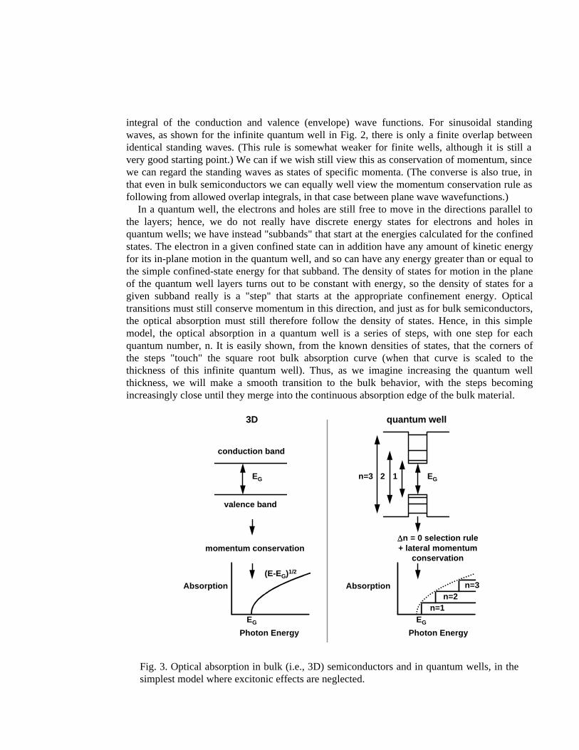
integral of the conduction and valence (envelope) wave functions. For sinusoidal standingwaves, as shown for the infinite quantum well in Fig. 2, there is only a finite overlap betweenidentical standing waves. (This rule is somewhat weaker for finite wells, although it is still avery good starting point.) We can if we wish still view this as conservation of momentum, sincewe can regard the standing waves as states of specific momenta. (The converse is also true, inthat even in bulk semiconductors we can equally well view the momentum conservation rule asfollowing from allowed overlap integrals, in that case between plane wave wavefunctions.)
In a quantum well, the electrons and holes are still free to move in the directions parallel tothe layers; hence, we do not really have discrete energy states for electrons and holes inquantum wells; we have instead "subbands" that start at the energies calculated for the confinedstates. The electron in a given confined state can in addition have any amount of kinetic energyfor its in-plane motion in the quantum well, and so can have any energy greater than or equal tothe simple confined-state energy for that subband. The density of states for motion in the planeof the quantum well layers turns out to be constant with energy, so the density of states for agiven subband really is a "step" that starts at the appropriate confinement energy. Opticaltransitions must still conserve momentum in this direction, and just as for bulk semiconductors,the optical absorption must still therefore follow the density of states. Hence, in this simplemodel, the optical absorption in a quantum well is a series of steps, with one step for eachquantum number, n. It is easily shown, from the known densities of states, that the corners ofthe steps "touch" the square root bulk absorption curve (when that curve is scaled to thethickness of this infinite quantum well). Thus, as we imagine increasing the quantum wellthickness, we will make a smooth transition to the bulk behavior, with the steps becomingincreasingly close until they merge into the continuous absorption edge of the bulk material.
n=3 2 1
conduction band
valence band
EG EG
EG
n=3n=2
n=1EG
3D quantum well
Absorption Absorption
Photon Energy Photon Energy
momentum conservation''n = 0 selection rule+ lateral momentum
conservation
(E-EG)1/2
Fig. 3. Optical absorption in bulk (i.e., 3D) semiconductors and in quantum wells, in thesimplest model where excitonic effects are neglected.
2.2. CONSEQUENCES OF HEAVY AND LIGHT HOLES
As we mentioned above, there are two kinds of holes that are relevant here, corresponding tothe heavy and light hole bands. Since these holes have different masses, there are two sets ofhole subbands, with different energy spacings. The light hole subbands, because they havelighter mass, are spaced further apart. The consequence for optical absorption is that there areactually two sets of "steps". The heavy-hole-to-conduction set starts at a slightly lower energyand is more closely spaced than the light-hole-to-conduction set. The heavy hole set is usuallydominant when we look at optical absorption for light propagating perpendicular to the quantumwell layers.
If, however, we look in a waveguide, with light propagating along the quantum well layers,there are two distinct optical polarization directions: one with the optical electric vector parallelto the quantum well layers (so-called "transverse electric" or TE polarization); and the otherwith the optical electric vector perpendicular to the quantum well layers (so-called "transversemagnetic" or TM polarization). The TE case is essentially identical to the situation for lightpropagating perpendicular to the layers, where the optical electric vector is always in the planeof the quantum wells; the optical electric vector is always perpendicular to the direction ofpropagation for a plane wave. The TM case is substantially different from the TE case, however.
Because of microscopic selection rules associated with the unit cell wavefunctions, for theTM polarization, the heavy-hole-to-conduction transitions are forbidden, and all of theabsorption strength goes over to the light-hole-to-conduction transitions. Hence, at least withthis simple model, there is now only one set of steps in the absorption. The reason for loss of theheavy hole transitions is not a special property of quantum wells; this kind of selection rule is aconsequence of defining a definite symmetry axis in the material, in this case the growthdirection of the quantum well layers. Exactly the same selection rule phenomenon will result ifwe apply a uniaxial stress to a bulk semiconductor. One practical consequence of this selectionrule effect is that quantum well waveguide lasers essentially always run in TE polarization;there are more heavy holes than light holes in thermal equilibrium, and hence the gainassociated with heavy holes is larger, and hence the gain is larger for the TE polarization. Ingeneral, this simple classification of holes into "heavy" and "light" is only valid near the centerof the Brillouin zone. The detailed structure of the valence bands is particularly complicatedsince the various subbands would actually appear to cross one another. In fact, such crossing areavoided, and the resulting subband structure is quite involved. For many devices, such effectsare not very important (at least for a basic understanding of the devices), and we will not discusssuch valence band effects further here.
2.3. OPTICAL ABSORPTION INCLUDING EXCITONS
Fig. 4 shows an actual absorption spectrum of a quantum well sample.We see from Fig. 4 that the quantum well absorption is indeed a series of steps, and simple
calculations based on the particle-in-a-box models will correctly give the positions of the steps.But it is also clear that there are sets of peaks in the spectra not predicted or explained by thesimple "non-excitonic" model described above. These peaks are quite a strong effect, and willbe particularly important near the band-gap energy, here at about 1.46 eV photon energy. Mostof the devices we discuss here operate in this region.
To understand these peaks, we need to introduce the concept of excitons. The key pointmissing in the previous discussion is that we have neglected the fact the electrons and holes are

charged particles (negative and positive respectively) that attract each other. Hence, when wehave an electron and a hole in a semiconductor, their wavefunctions are not plane waves; planewaves correspond to the case of uniform independent motion of the electron and the hole.Instead, we should expect that the electron and hole wavefunction should correspond to the casewhere the electron and hole are close to one another because of their Coulomb attraction. Theformal error we made in the analysis above is therefore that we did not use the correcteigenfunctions for the electrons and holes, and hence we formally got an incorrect answer whenwe used those eigenfunctions to calculate the optical absorption.
1.46 1.54 1.62 1.70
5
10
15
20
Abs
orpt
ion
(10
cm
)
3-1
Photon Energy (eV)
Fig. 4. Absorption spectrum of a typical GaAs/AlGaAs quantum well structure at roomtemperature.
Unfortunately, to include excitonic effects properly we need to use a different picture, sincethe whole band structure picture is a single particle picture; it essentially describes the energiesseen by either a single electron or a single hole, but cannot handle both at once. Fortunately,there is a simple picture that allows us to understand the resulting excitonic effects.
The correct approach is not to consider raising an electron from the valence band to theconduction band, but rather to consider the creation of an electron-hole pair. In this picture, wefind the eigenfunctions of the electron-hole pair in the crystal, and base our calculation ofoptical absorption on those pair states. First, then, we must understand what are the states of anelectron-hole pair in a crystal. Fortunately, at least for the case where the attraction is not toostrong, this problem is already solved; it is essentially the same problem as the states of thehydrogen atom, corrected for the different effective masses and dielectric constants in thesemiconductor. Using this model, we find, for example, the binding energy of lowest, 1S,exciton is
Ee
hBR o
P
H H
4
2 2 28(3)

where h is Planck's constant, HR is the relative permittivity, Ho is the permittivity of free space,and P is the reduced mass
P
�
m m
m me h
e h
(4)
For bulk GaAs (where excitons can be clearly seen at low temperature), EB ~ 4 meV.Hence, we find the first remarkable property of excitons compared to the non-excitonic
model. It is possible to create an exciton with an energy EB less than that required to create a"free" electron-hole pair. A free electron-hole pair is analogous to an ionized hydrogen atom,and the energy required to create such a free pair in the semiconductor is actually the simpleband-gap energy of the single particle picture. Hence we expect some optical absorption atphoton energies just below the band-gap energy. This point is illustrated in Fig. 5, on the left,showing a possible transition at an energy Eexciton = Ebandgap - EB.
It is not only the absorption that creates the 1S exciton that is important, although under mostconditions it is the only one that we see clearly as a distinct peak. In fact the entire absorptionspectrum of these kinds of semiconductors is properly described in terms of the complete set ofhydrogenic states. For example, the absorption above the band-gap energy results from thecreation of excitons in the unbound hydrogenic states. In the classical sense, such statescorrespond to hyperbolic orbits. There is also additional absorption just below the bandgapenergy from the other, bound excitonic states.
Note now that we are explaining the optical absorption in terms of the creation of a particle,the exciton (or, exactly equivalently, an electron-hole pair). It is important to understand that theabsorption we see is not that associated with raising an existing hydrogenic particle to anexcited state, as would be the case with conventional atomic absorption; we are instead creatingthe particle. An analogy that may help understand this distinction is the absorption in thevacuum that creates electron-positron pairs. This is illustrated in Fig. 5, on the right.
By absorbing photons in the vacuum, we can in principle create positronium atoms, whichare simply hydrogenic systems composed of an electron and a positron (instead of a proton). Inthis case, we are simultaneously creating a positron in the Fermi sea (the analog of the valenceband), as well as an electron. This happens to be a two-photon transition, and is therefore arather weak effect in practice, but it illustrates the difference between the creation of an atomand the absorption between levels of the atom. A very important difference between these is thatin the creation case, we have "excitonic" absorption even when we have no excitons in thematerial. In the positronium case, it is very clear that there need be no positronium atoms theresince we are starting with a perfect vacuum!
In the simple model where we neglected excitonic effects, the strength of a particulartransition was determined by the square of the overlap integral between the "initial" (valencesubband) state and the "final" (conduction subband) state. In principle, we have a similar resultfor the present excitonic model, although in this case the initial state is the "empty" crystal, andthe final state is the crystal with an exciton added. We will not formally derive the consequencesof this change in model, but the net result is that, in the exciton creation case, the strength of theabsorption to create an electron-hole pair in a given state is proportional to the probability thatthe resulting electron and hole will be in the place (strictly, the same unit cell). Now we canunderstand why the excitonic absorption gives such a strong peak for creation of 1S excitons. Inthe 1S exciton, the electron and hole are bound closely to one another (within a diameter ofabout 300 Å in bulk GaAs), and the 1S wavefunction actually peaks at zero relative

displacement. Hence the probability of finding the electron and the hole in the same place isactually very large, and so the resulting absorption is strong.
conduction band
valence band
Eexciton
EB4 meV
Ebandgap 1.5 eV
free electrons
electron “sea”
Epositronium
EB6.8 eV
Efree pair1.022 MeV
semiconductor vacuum
absorption at photon energyEexciton creates excitons
(two photon) absorption ofenergy Epositronium createsatom
Fig. 5. Analogy between excitonic absorption and the optical creation of positroniumatoms.
Thus far, we have discussed excitons in general, without explaining why they are particularlyimportant in quantum wells. Excitonic effects are clear in many direct gap semiconductors atlow temperature. At room temperature, however, although excitonic effects are still veryimportant in determining the shape and strength of the interband absorption, the actual peakscorresponding to the bound states are difficult to resolve. The main reason for this lack ofresolution is that the bound states are rapidly ionized by collisions with optical phonons at roomtemperature. In fact, they are typically ionized in times short compared with a classical orbittime. By a Heisenberg uncertainty principle argument, the associated optical linewidth isbroadened, to such a point that the line is no longer clearly resolvable.
The quantum well offers two important differences compared to the bulk material, both ofwhich stem from the confinement in the quantum well. Fig. 6 shows, in a semiclassical picture,an exciton in bulk GaAs and an exciton in a quantum well.Hydrogenic theory for the GaAs exciton gives a diameter of about 300 Å, as mentioned above.When we create an exciton in a quantum well that is only 100 Å thick, the exciton must becomesmaller, at least in the direction perpendicular to the quantum wells. Remarkably, however, italso becomes smaller in the other two directions (in the plane of the quantum well). Thissurprising conclusion can be checked, for example, by variational calculations. We canrationalize it by saying that nature prefers to keep the exciton more nearly spherical to minimizeenergy overall. If, for example, we allowed the exciton to become a flat "pancake" shape, itwould acquire high kinetic energies from the large second derivatives at the edges of thepancake. It is also the case that the exact solution of the two-dimensional hydrogen atom,corresponding to a very thin quantum well with very high walls, has a diameter one quarter thatof the three-dimensional hydrogen atom. The two consequences are: (1) the electron and holeare even closer together than in the three-dimensional case, so the absorption strength to create
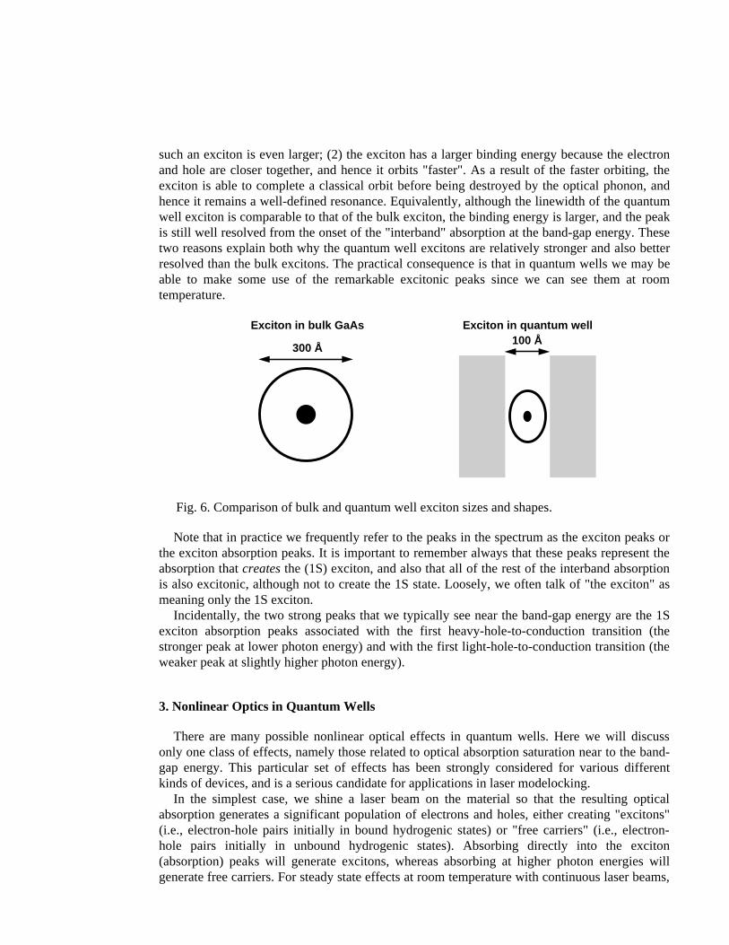
such an exciton is even larger; (2) the exciton has a larger binding energy because the electronand hole are closer together, and hence it orbits "faster". As a result of the faster orbiting, theexciton is able to complete a classical orbit before being destroyed by the optical phonon, andhence it remains a well-defined resonance. Equivalently, although the linewidth of the quantumwell exciton is comparable to that of the bulk exciton, the binding energy is larger, and the peakis still well resolved from the onset of the "interband" absorption at the band-gap energy. Thesetwo reasons explain both why the quantum well excitons are relatively stronger and also betterresolved than the bulk excitons. The practical consequence is that in quantum wells we may beable to make some use of the remarkable excitonic peaks since we can see them at roomtemperature.
300 Å100 Å
Exciton in bulk GaAs Exciton in quantum well
Fig. 6. Comparison of bulk and quantum well exciton sizes and shapes.
Note that in practice we frequently refer to the peaks in the spectrum as the exciton peaks orthe exciton absorption peaks. It is important to remember always that these peaks represent theabsorption that creates the (1S) exciton, and also that all of the rest of the interband absorptionis also excitonic, although not to create the 1S state. Loosely, we often talk of "the exciton" asmeaning only the 1S exciton.
Incidentally, the two strong peaks that we typically see near the band-gap energy are the 1Sexciton absorption peaks associated with the first heavy-hole-to-conduction transition (thestronger peak at lower photon energy) and with the first light-hole-to-conduction transition (theweaker peak at slightly higher photon energy).
3. Nonlinear Optics in Quantum Wells
There are many possible nonlinear optical effects in quantum wells. Here we will discussonly one class of effects, namely those related to optical absorption saturation near to the band-gap energy. This particular set of effects has been strongly considered for various differentkinds of devices, and is a serious candidate for applications in laser modelocking.
In the simplest case, we shine a laser beam on the material so that the resulting opticalabsorption generates a significant population of electrons and holes, either creating "excitons"(i.e., electron-hole pairs initially in bound hydrogenic states) or "free carriers" (i.e., electron-hole pairs initially in unbound hydrogenic states). Absorbing directly into the exciton(absorption) peaks will generate excitons, whereas absorbing at higher photon energies willgenerate free carriers. For steady state effects at room temperature with continuous laser beams,
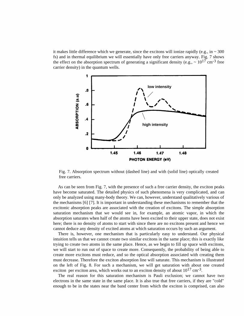
it makes little difference which we generate, since the excitons will ionize rapidly (e.g., in ~ 300fs) and in thermal equilibrium we will essentially have only free carriers anyway. Fig. 7 showsthe effect on the absorption spectrum of generating a significant density (e.g., ~ 1017 cm-3 freecarrier density) in the quantum wells.
low intensity
high intensity
Fig. 7. Absorption spectrum without (dashed line) and with (solid line) optically createdfree carriers.
As can be seen from Fig. 7, with the presence of such a free carrier density, the exciton peakshave become saturated. The detailed physics of such phenomena is very complicated, and canonly be analyzed using many-body theory. We can, however, understand qualitatively various ofthe mechanisms [6] [7]. It is important in understanding these mechanisms to remember that theexcitonic absorption peaks are associated with the creation of excitons. The simple absorptionsaturation mechanism that we would see in, for example, an atomic vapor, in which theabsorption saturates when half of the atoms have been excited to their upper state, does not existhere; there is no density of atoms to start with since there are no excitons present and hence wecannot deduce any density of excited atoms at which saturation occurs by such an argument.
There is, however, one mechanism that is particularly easy to understand. Our physicalintuition tells us that we cannot create two similar excitons in the same place; this is exactly liketrying to create two atoms in the same place. Hence, as we begin to fill up space with excitons,we will start to run out of space to create more. Consequently, the probability of being able tocreate more excitons must reduce, and so the optical absorption associated with creating themmust decrease. Therefore the exciton absorption line will saturate. This mechanism is illustratedon the left of Fig. 8. For such a mechanism, we will get saturation with about one createdexciton per exciton area, which works out to an exciton density of about 1017 cm-3.
The real reason for this saturation mechanism is Pauli exclusion; we cannot have twoelectrons in the same state in the same place. It is also true that free carriers, if they are "cold"enough to be in the states near the band center from which the exciton is comprised, can also

prevent creation of more excitons, again by the Pauli exclusion principle. This is illustrated onthe right of Fig. 8.
excitons filling space free carriers filling space
Fig. 8. Illustration of saturation by filling space with excitons (left) and filling space withfree carriers. At a density of one exciton per exciton volume, or one "cold" free carrierper exciton volume, it becomes essentially impossible to create any more excitons. Thiscan be visualized geometrically in terms of the probability of trying to "throw" one moreexciton onto the plane without it landing on any of the other excitons or free carriers.
Although we have discussed the saturation mechanisms so far in a qualitative and simplisticway, it turns out that these mechanisms are rigorously correct, with the only detail being theeffective area of the exciton to use in the argument [7]. There are also other mechanisms that aresomewhat less obvious, and some of these are of comparable size [7]. A second class ofmechanisms that will change the absorption is screening effects. If we create a density of freecarriers, they will tend to change the dielectric constant, and hence change the size of theexciton, typically increasing it. If the size of the exciton increases, then the probability offinding the electron and hole in the same place decreases; hence the optical absorption strengthdecreases, giving an effect that also behaves like saturation. This direct, classical Coulombscreening is thought to be weak in quantum wells because the walls of the wells prevent themovement of charge necessary for effective screening. There is, however, an even more subtleeffect that is actually of comparable size to the other "saturation" mechanisms, which isexchange screening. Essentially, when we include the effect of Pauli exclusion in ourcalculations, we find that the results we would calculate using our simple classical Coulombeffects are not correct at high density, because the Pauli exclusion forces the electrons to befurther apart than we had thought (and similarly for the holes). This is described as if it were ascreening effect, although it is actually a Pauli exclusion effect that causes us to correct ourprevious Coulomb calculation. This exchange screening also tends to increase the size of theexciton, reducing absorption.
Although in the steady state at room temperature, we see primarily the effect of free carrierson excitons, at lower temperatures or at short time scales we can see the effect of excitons onexcitons. These latter effects are actually typically somewhat stronger (e.g., a factor of 1.5 - 2).Hence, if we initially create excitons and monitor the saturation of the exciton peaks, we can seea fast transient absorption saturation associated with the exciton-exciton effects, followed by asomewhat weaker saturation as the excitons ionize. This actually allows us to measure theexciton ionization time, which is about 300 fs at room temperature.
These saturation effects associated with the exciton peak in quantum wells are relativelysensitive. They have been explored for a variety of nonlinear optical switching devices. Even
with the additional benefits of the strong quantum well excitons, these effects are not largeenough to make low enough energy devices for current practical systems interest forinformation processing. The effects are important, however, for two reasons. One reason is thatthey set limits on the operating power of other devices, such as the modulators andelectroabsorptive switches discussed below. Secondly, the effects are large enough for serioususe as mode locking saturable absorber elements for lasers, and this is becoming practical now[8].
4. Quantum Well Electroabsorption Physics
When electric fields are applied to quantum wells, their optical absorption spectrum near tothe band-gap energy can be changed substantially, an effect we can call electroabsorption. Sucheffects have been extensively investigated for optical modulators and switches [9]. There aretwo very distinct directions in which we can apply electric fields to quantum wells, either withthe electric fields parallel to the layers or with the electric field perpendicular to the layers. Thecase of fields perpendicular to the layers is the one most peculiar to quantum wells, and it iscalled the Quantum-Confined Stark Effect (QCSE). Here, we will first discuss the case of fieldsparallel to the layers.
4.1. ELECTRIC FIELDS PARALLEL TO THE LAYERS
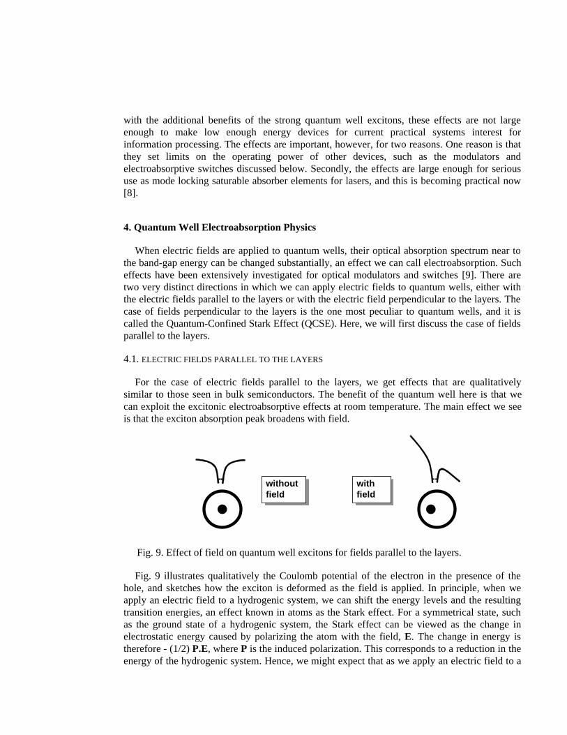
For the case of electric fields parallel to the layers, we get effects that are qualitativelysimilar to those seen in bulk semiconductors. The benefit of the quantum well here is that wecan exploit the excitonic electroabsorptive effects at room temperature. The main effect we seeis that the exciton absorption peak broadens with field.
withoutfield
withfield
Fig. 9. Effect of field on quantum well excitons for fields parallel to the layers.
Fig. 9 illustrates qualitatively the Coulomb potential of the electron in the presence of thehole, and sketches how the exciton is deformed as the field is applied. In principle, when weapply an electric field to a hydrogenic system, we can shift the energy levels and the resultingtransition energies, an effect known in atoms as the Stark effect. For a symmetrical state, suchas the ground state of a hydrogenic system, the Stark effect can be viewed as the change inelectrostatic energy caused by polarizing the atom with the field, E. The change in energy istherefore - (1/2) P.E, where P is the induced polarization. This corresponds to a reduction in theenergy of the hydrogenic system. Hence, we might expect that as we apply an electric field to a

semiconductor, we should see the 1S exciton absorption peak move to lower energies, becausethe energy of the resulting exciton we create is lower by this Stark shift.
It is true that there is such a Stark shift, but it is not the dominant effect that we see. Thereason is that the Stark shift of a hydrogenic system is limited to about 10% of the bindingenergy. Since the binding energy of the exciton is only about 10 meV, the shift is thereforelimited to about 1 meV, and hence it is not a very large effect. When we try to shift the energyby more than this, the hydrogenic system becomes field ionized (i.e., the electron and hole are"ripped" apart by the field) so rapidly that the particle cannot complete even a substantialfraction of a classical orbit before being destroyed, and the whole concept of a bound state losesany useful meaning. In fact, what we see primarily as we apply the field is the broadening of theexciton absorption resonance caused by the shortening of the exciton's lifetime - again, a"Heisenberg uncertainty principle" broadening. (It is just possible to see the shift at low fields ina carefully controlled experiment.)
0 V / cm
16 kV / cm
48 kV / cm
Fig. 10. Absorption spectra for a quantum well sample at room temperature with variouselectric fields applied in the plane of the quantum well layers. The spectra are shiftedvertically for clarity. The exciton peaks broaden with field.
It is worth noting that the fields we are capable of applying to the exciton are gigantic in arelative sense. Applying 1V / Pm ( = 104 / cm) corresponds to a field of one binding energy (~10 meV) over one exciton diameter (~ 100 Å). Such a field corresponds to a massiveperturbation, certainly much larger than can readily be achieved with a hydrogen atom itself. Itis also not surprising that such a field should cause the exciton to be field-ionized in less than aclassical orbit time.
Fig. 10 shows a typical set of spectra for parallel field electroabsorption in quantum wells.The broadening and disappearance of the peaks is clearly seen. One consequence is theappearance of a weak absorption tail at lower photon energies. The appearance of this tail isoften referred to as the Franz-Keldysh effect. This is somewhat misleading, however, since the
Franz-Keldysh effect is really a non-excitonic effect, whereas excitonic effects dominate near tothe band-gap energy; the Franz-Keldysh effect, for example, cannot model the excitonbroadening at all.
4.2. ELECTRIC FIELDS PERPENDICULAR TO THE LAYERS
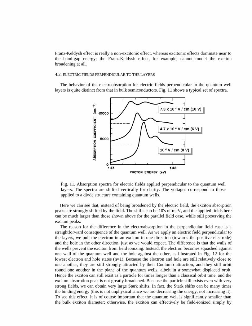
The behavior of the electroabsorption for electric fields perpendicular to the quantum welllayers is quite distinct from that in bulk semiconductors. Fig. 11 shows a typical set of spectra.
10 4 V / cm (0 V)
4.7 x 10 4 V / cm (6 V)
7.3 x 10 4 V / cm (10 V)
Fig. 11. Absorption spectra for electric fields applied perpendicular to the quantum welllayers. The spectra are shifted vertically for clarity. The voltages correspond to thoseapplied to a diode structure containing quantum wells.
Here we can see that, instead of being broadened by the electric field, the exciton absorptionpeaks are strongly shifted by the field. The shifts can be 10's of meV, and the applied fields herecan be much larger than those shown above for the parallel field case, while still preserving theexciton peaks.
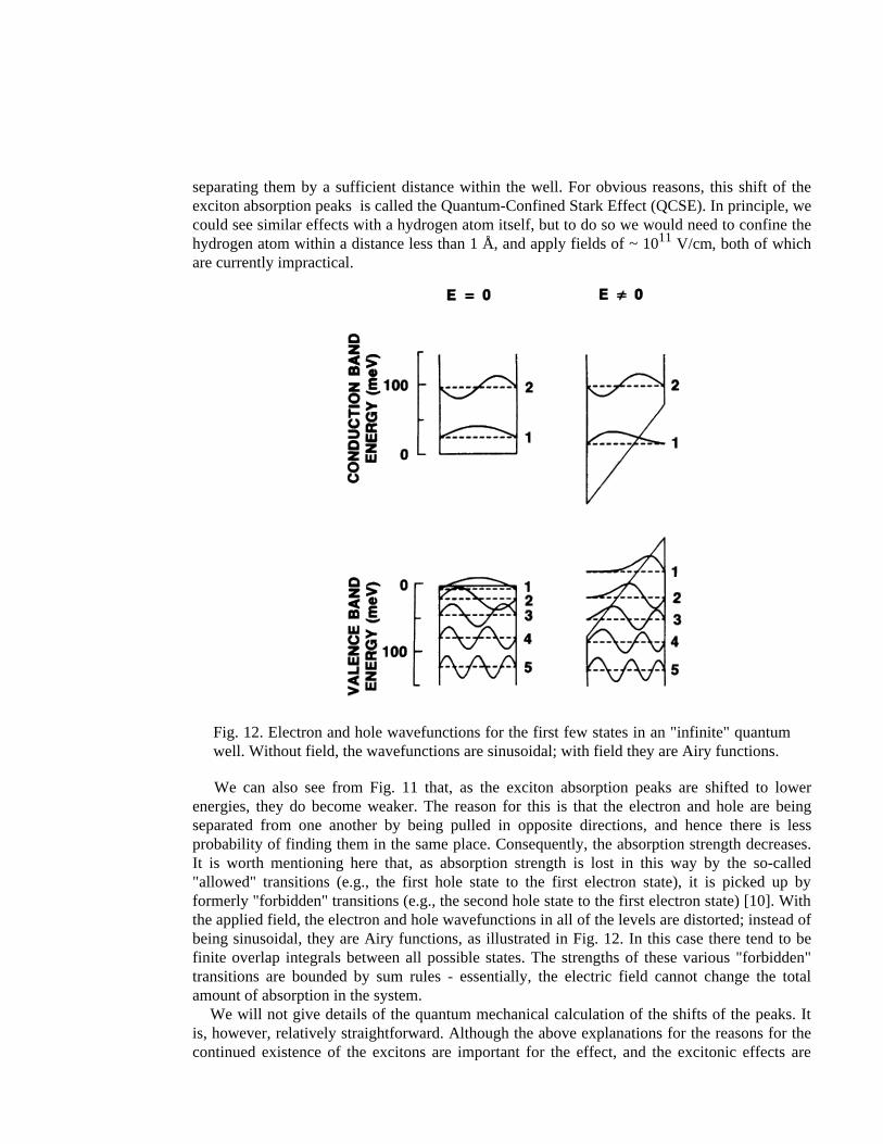
The reason for the difference in the electroabsorption in the perpendicular field case is astraightforward consequence of the quantum well. As we apply an electric field perpendicular tothe layers, we pull the electron in an exciton in one direction (towards the positive electrode)and the hole in the other direction, just as we would expect. The difference is that the walls ofthe wells prevent the exciton from field ionizing. Instead, the electron becomes squashed againstone wall of the quantum well and the hole against the other, as illustrated in Fig. 12 for thelowest electron and hole states (n=1). Because the electron and hole are still relatively close toone another, they are still strongly attracted by their Coulomb attraction, and they still orbitround one another in the plane of the quantum wells, albeit in a somewhat displaced orbit.Hence the exciton can still exist as a particle for times longer than a classical orbit time, and theexciton absorption peak is not greatly broadened. Because the particle still exists even with verystrong fields, we can obtain very large Stark shifts. In fact, the Stark shifts can be many timesthe binding energy (this is not unphysical since we are decreasing the energy, not increasing it).To see this effect, it is of course important that the quantum well is significantly smaller thanthe bulk exciton diameter; otherwise, the exciton can effectively be field-ionized simply by
separating them by a sufficient distance within the well. For obvious reasons, this shift of theexciton absorption peaks is called the Quantum-Confined Stark Effect (QCSE). In principle, wecould see similar effects with a hydrogen atom itself, but to do so we would need to confine thehydrogen atom within a distance less than 1 Å, and apply fields of ~ 1011 V/cm, both of whichare currently impractical.
Fig. 12. Electron and hole wavefunctions for the first few states in an "infinite" quantumwell. Without field, the wavefunctions are sinusoidal; with field they are Airy functions.
We can also see from Fig. 11 that, as the exciton absorption peaks are shifted to lowerenergies, they do become weaker. The reason for this is that the electron and hole are beingseparated from one another by being pulled in opposite directions, and hence there is lessprobability of finding them in the same place. Consequently, the absorption strength decreases.It is worth mentioning here that, as absorption strength is lost in this way by the so-called"allowed" transitions (e.g., the first hole state to the first electron state), it is picked up byformerly "forbidden" transitions (e.g., the second hole state to the first electron state) [10]. Withthe applied field, the electron and hole wavefunctions in all of the levels are distorted; instead ofbeing sinusoidal, they are Airy functions, as illustrated in Fig. 12. In this case there tend to befinite overlap integrals between all possible states. The strengths of these various "forbidden"transitions are bounded by sum rules - essentially, the electric field cannot change the totalamount of absorption in the system.
We will not give details of the quantum mechanical calculation of the shifts of the peaks. Itis, however, relatively straightforward. Although the above explanations for the reasons for thecontinued existence of the excitons are important for the effect, and the excitonic effects are

also important for the strength of the absorption, the dominant part of the shift comes from theunderlying shift of the single particle states. We can see this shift in Fig. 12, where we see then=1 electron level moving down and the n=1 hole level moving up; the net result is that theenergy separation between the n=1 hole and electron levels is reduced with field. The shift inthe exciton binding energy itself is relatively unimportant by comparison (typically a few meV).The calculation of the shift of individual electron or hole levels with field can be done byvarious means. For a tilted well, the wave equation becomes Airy's differential equation, andhence the exact solutions (e.g., as in Fig. 12) are Airy functions.
It is also, incidentally, quite correct to view the quantum-confined Stark effect shifts asresulting from the polarization of the exciton by the electric field, hence giving a (1/2) P.E shiftin the exciton energy. To lowest order, the polarization is proportional to the field (i.e., theinduced separation of the electron and hole is initially linear with field), and so the QCSE is aquadratic effect to lowest order.
Although we have discussed effects here only for the case of simple "rectangular" quantumwells, many other forms of quantum wells are also possible, such as coupled quantum wells,graded quantum wells, stepped quantum wells. These other structures also show related effectsinduced by applied electric fields, although we will not discuss these here. Also, superlatticesshow a class of effects induced by fields, known as Wannier-Stark localization. This effect andeffects in coupled quantum wells are closely related.
5. Quantum Well Modulators
The QCSE is particularly attractive for optical modulators. A simple device structure isshown in Fig. 13. A quantum well region, typically containing 50 to 100 quantum wells, isgrown as the undoped "intrinsic" ("i") region in a p-i-n diode. This quantum well region willtherefore have a thickness of about 1 - 2 microns. In operation, the diode is reverse biased. 1 Vacross 1 micron corresponds to a field of 104 V/cm, so substantial QCSE shifts and changes inthe absorption spectrum can be made with applied voltages of the order of 5 - 10 V. The reversebiased diode is convenient because there is no conduction current that needs to flow in the diodein order to apply these relatively substantial fields.
The "p" and "n" regions of the diode are made out of a material that is substantiallytransparent at the wavelength of interest. In the case of GaAs quantum wells, they would mostlikely be made out of AlGaAs, the same material as used for the quantum well barriers. For theparticular case of GaAs/AlGaAs quantum wells, the usual substrate material is GaAs.Unfortunately, GaAs is opaque at the wavelengths used with such modulators, hence thesubstrate has to be removed for a transmissive modulator, such as the one in Fig. 13.
There are two very important features of the quantum well modulator. The first is that theelectroabsorptive mechanisms (the QCSE) in the quantum well are strong enough to make amodulator that can work for light propagating perpendicular to the surface of thesemiconductor. Despite the fact that this modulator will typically only be a few microns inthickness altogether, it can make changes in transmission of a factor of 2 - 3 in a single pass of alight beam. This modulation is large enough to make usable systems. This feature has the veryimportant consequence that one can therefore make two-dimensional arrays of devices. Thisopens up many possibilities for novel highly-parallel optoelectronic systems.

SL
Q
�YH
�YH
VXEVWUDWH�Q�*D$V�
ERWWRP FRQWDFW�Q�$O*D$V�
TXDQWXP ZHOOV�XQGRSHG�
WRS FRQWDFW�S�$O*D$V�
OLJKW LQOLJKW RXW
Fig. 13. Quantum well modulator diode structure.
A second key feature is that the operating energy of this modulator is small. The amount ofenergy required to change the optical properties in this modulator is essentially the storedelectrostatic energy at the operating field. In other words, one has to charge up the capacitanceof the device. The capacitance of a 1 micron square area of a semiconductor device 1 micronthick is approximately 10-16 F. Hence the total energy required to charge the device is (1/2) CV2
~ 1 - 2 fJ/Pm2. This energy density is comparable to the energy density in switching electronicdevices, and is much smaller (e.g., by a factor of ~ 100) than the energy per unit optical arearequired to turn on a laser diode or saturate an optical absorption. Hence this device is veryattractive as a potentially highly efficient optical output device for electronic circuits.
In addition, the speed limit on the use of the QCSE is probably in the range of ~ 100 fs orless. Practical modulator devices will not be limited by the electroabsorption mechanism itself,seeing instead only the usual resistive/capacitive limits in applying voltage to the diodes.Because the diodes can be small, the capacitance can also be small, and hence these devices areattractive for high speed modulators.
Although we will discuss here primarily only devices where the light propagatesperpendicular to the surface, the QCSE can also be used effectively for waveguide modulators(where the light propagates along the surface). In this case, a useful modulator can be made withonly a few quantum wells because the propagation distance can be long (e.g., 100 microns). As aresult, waveguide quantum well modulators can operate with low voltages (e.g., < 1 V).
The removal of the substrate, as shown in Fig. 13, is usually undesirable since it leaves a verythin structure. An alternative is to grow the quantum well modulator on top of a mirror [11].Such a mirror can be made directly in the semiconductor growth machine by making amultilayer dielectric stack mirror from the semiconductor materials themselves. Such atechnique leaves a crystalline surface suitable for the epitaxial growth of the quantum welldevice. The semiconductor layers do not have a large index contrast between them, however, soa relatively large number of pairs of quarter-wave layers is usually required (e.g., 12 - 20 pairsof layers, each layer ~ 800 Å thick). A second consequence of the small index contrast is thatthe mirror has a relatively narrow wavelength band for reflection (e.g., < 100 nm at 850 nmwavelength). As a result, the control of the thickness of the mirror layers often imposes tighter

tolerance on the growth rate than does the thickness of the quantum well layers themselves.(The exciton peak shifts relatively little for a change of a few percent in the layer thickness,whereas such a percentage change in the mirror thicknesses could move the reflection bandaway from the operating wavelength region.)
OO / 4 AlGaAs
OO / 4 AlAsmultilayerdielectricstackmirror
substrate
quantum wells
p - AlGaAs
n - doped
anti-reflectioncoating
light in light out
Fig. 14. Quantum well reflection modulator.
The reflection modulator also brings other benefits. It improves the contrast ratio (actuallysquaring it compared to a simple modulator), because the light beam makes two passes throughquantum well material. The structure also permits conventional electronic chip mounting andsubstrate heat sinking because we do not have to pass light through the bottom of the chip.
Table 1
An extension of the reflective modulator concept is to put the modulator inside a resonantcavity by adding a reflecting surface on top. One interesting design is the asymmetric Fabry-Perot resonator [12]. In this case, the bottom reflector is made more reflecting than the topreflector. When the right amount of absorption is created inside the resonator, the bottomreflector "looks" as if it has the same reflection as the top reflector. In any Fabry-Perot resonator
Some Quantum Well Modulator Material SystemsMaterials Typical Wavelength
GaAs/GaAlAs 850 nmInGaAs/InP 1.5Pm
GaSb/GaAlSb 1.5PmInGaAs/GaAs 980 nm, 1.06 Pm
InAsP/InP 1.06 PmAlGaAs/AlAs 680 nmInGaAsP/InP 1.3 PmCdZnTe/ZnTe 610 nm

with equal front and back mirror reflectivities, in the on-resonance condition there is exactly noreflection from the resonator. Hence by increasing or reducing the absorption in the quantumwell layers to exactly the right amount, the modulator structure has exactly no reflection. Thiscan give a modulator with very high contrast ratio and also lower drive voltage since typicallyless absorbing material is required than in the non-resonant case. The major practical problemwith this concept is that, since the idea only works on resonance, the thicknesses of the layershave to be very precisely controlled during fabrication, a formidable task for current growthtechniques.
Quantum well modulators have been demonstrated in many material systems and at manywavelengths. Table 1 shows a list of some of the materials and the operating wavelengths.
The quantum well modulators can be run in two different modes, illustrated in Fig. 15. In theso-called "O0" mode, the absorption decreases with increasing reverse bias voltage. Theoperating wavelength is then typically chosen to coincide with the position of the excitonabsorption peak near zero bias. In the "O1" mode, the absorption increases with increasingreverse bias. Note, incidentally, that by applying enough voltage, e.g., 10 V in Fig. 15, theoperation at the indicated "O1" wavelength ends up by also showing a decrease of absorptionwith reverse voltage once the exciton peak has moved past the operating wavelength.
835 840 845 850 855 860 865 870 875
0
5000
10000
15000
20000
25000
V = 10 V
V = 5 V
V = 0 V
Abs
orpt
ion
(a.u
.)
Wavelength (nm)
Absorption increasewith voltage
Absorption decreasewith voltage
OO����
OO����
Fig. 15. Illustration of the two characteristic operating wavelengths of quantum wellmodulators. At O0, the modulator absorption decreases with increasing reverse biasvoltage. At O1, the absorption increases with voltage.
Most obviously the choice of mode affects whether the modulator increases or decreasestransmission (or reflection) as voltage is applied. There are, however, other consequences of thechoice of mode. One relates to the maximum power that can be applied to the modulatorswithout saturation. When running at O1, whenever there is absorption in the modulator there isalso substantial electric field over the quantum wells. The electric field tends to cause the
carriers to escape from the wells rapidly [13][14], and so they tend not to build up in the wells.Carrier build-up in the wells can cause saturation of the absorption. Hence this O1 operation hashigher saturation intensities [15]. This can be important in practice; for example, the presentdesign of modulators for the FET-SEED devices (discussed below) is intended to handle 500PW incident power at 850 nm wavelength in a 3 Pm diameter spot, corresponding to intensitiesof the order of 5 - 10 kW/cm2.
The second important point about the choice of operating mode relates to the feedbackinduced in the modulator circuit by the photocurrent generated in the quantum well diode.Depending on the details of the electrical circuit, the photocurrent generated in the modulatortends to change the voltage across the modulator, hence changing the absorption, and hence inturn changing the photocurrent. Operating at O0 tends to give positive feedback that can lead tobistability. Operating at O1 tends to give negative feedback that can lead to linearizedmodulation. These feedback effects will be discussed below in the section on self-electroopticeffect devices (SEEDs).
The quantum well modulator can also be used to make changes in refractive index. As is wellknown, changes in absorption spectrum generally lead to changes in the refractive indexspectrum, the two being related by the Kramers-Krönig relations. As a result, there is arefractive index change associated with the QCSE [16]. This effect can also be used to makedevices, such as electro-optic modulators [17]. One problem with using refractive effects is thatwe cannot normally use the refractive effects in those spectral regions where they are largest,such as close to the exciton absorption peaks. The reason is that refractive devices usuallyrequire that we can make more than half a wavelength of path length change in less than oneabsorption length, and the absorption is too strong near to the exciton peaks. Consequently, it isdifficult to make useful refractive devices that can be operated for light propagatingperpendicular to the surface (e.g., with ~ 1 Pm of optical thickness as in the absorptive p-i-nmodulator structure). As we move to longer wavelengths, however, the refractive effects fall offmore slowly than the absorption effects. Consequently, waveguide devices of about 100 Pm ormore of length can be made, and these are operated at wavelengths somewhat longer than theband-edge wavelength. Even these lengths are significantly shorter than those of otherwaveguide electro-optic modulators, and such devices offer the additional advantage that theycan be integrated with other semiconductor devices, such as lasers, photodetectors and opticalamplifiers.
6. Self-Electrooptic-Effect Devices
The Self Electrooptic Effect Device (SEED) principle is to combine a quantum wellmodulator (or a set of modulators) with a photodetector (or a set of photodetectors) to make anoptically controlled device with an optical output (or outputs) [18] [19]. A major reason forthinking about such a class of devices is an opportunity for efficient integration. Quantum wellmodulators driven directly by external electrical connections are limited in speed and operatingenergy by the external electrical parasitics, such as capacitance and the need to drive withimpedance matched lines at high speeds. The modulators themselves can be driven with verylow total energies if the drive is electrically local and not brought in by some externalconnection. Furthermore, since they are semiconductor devices, the prospects for integrationwith various optoelectronic and electronic devices are good.

Absorption
Photon Energy (eV)1.43 1.48
Vo
+
-
R
nip
MQW
low voltagehigh
voltage
Fig. 16. Illustration of operating photon energy (or wavelength) point and circuit forsimple resistive optical bistability.
Although it is often the case that the conversion from optics to electronics and back to opticsis inefficient and costly, this need not be the case if the devices are well integrated. In practice,the quantum well devices can be integrated effectively, and allow two-dimensional arrays ofsmart optoelectronic units or "smart pixels". Such devices offer new possibilities in informationprocessing and switching architectures.
TransmittedPower
Incident Power
decreasing diode voltage
bistableregion
discontinuous"switching"
Fig. 17. Characteristic bistable curve for the simple SEED circuit of Fig. 16.
There are two general classes of SEEDs, those based on diodes alone and those alsointegrating transistors. The simplest SEED configuration is shown in Fig. 16. This is a so-called"resistor-biased" SEED (R-SEED), and it is optically bistable. It is operated at O0 where theabsorption increases as the reverse bias voltage is reduced.
This device is optically bistable as shown in Fig. 17. The bistability results from a positivefeedback mechanism. Suppose initially there is little light shining on the diode. Then there islittle photocurrent, and consequently little voltage drop across the resistor. Hence the full supplyvoltage appears across the diode, and the absorption of the diode is relatively low. As we start toshine more light on the diode, we get more photocurrent. Because of the voltage drop nowacross the resistor, we get now less voltage across the diode, and hence more absorption, and

hence more photocurrent, and so on. As a result of this mechanism, we can get switching into ahighly absorbing state. Once in this state, the device requires less input power to hold it in thisstate because the diode is now so highly absorbing. Decreasing to some lower power eventuallyleads to a similar but opposite mechanism that causes the diode to switch back to its high-voltage, low transmission state, as shown in Fig. 17.
As an alternative to using a resistor as the "load" in the bistable circuit of Fig. 16, we coulduse another reverse-biased photodiode. The photodiode could then perform the function of theload resistor, but with an effective "resistance" value controlled by the light shining on thissecond, "load" photodiode. Such a circuit is called a "diode-biased" SEED (D-SEED), and it hasvarious interesting analog modes that we will discuss below. A further extension of this conceptis to use a second quantum well diode as the "load", giving the so-called "symmetric" SEED (S-SEED), as shown in Fig. 18 [20].
The S-SEED is unusual in that it is bistable in the ratio of the two input light beam powersrather than switching at any particular absolute power. We can analyze this device in a similarfashion to the R-SEED bistability; it has the same kind of intrinsic positive feedback. In the caseof the S-SEED, it switches simply when the photocurrent in one diode exceeds that in the other,and hence we can run the S-SEED over a very wide range of powers. We can run it at very lowabsolute powers, in which case it will switch slowly, or at high powers, in which case it willswitch rapidly. (The switching speed is determined by the charging and discharging of the diodecapacitances by the photocurrent.)
+
-
Fig. 18. Schematic of symmetric SEED (S-SEED)
The S-SEED is a particularly useful device for systems experiments. One very useful featureis "time-sequential gain". Put simply, we can switch the device when running it low powers andread it out at high powers, hence achieving effective gain, which is always required in logicsystems. Importantly, this "gain" does not require that we set the operating power particularlycarefully. Attempts to make logic systems with simple bistable devices have been very difficultbecause of the necessity of biasing very close to the switching point in order to get gain; the S-SEED avoids this problem. Another important feature of the S-SEED is that it providescomplementary and differential inputs and outputs. The logic value is represented not by anyparticular beam power, but by the ratio of two beam powers, a number that is independent ofattenuation. Attenuation of various kinds is unavoidable and sometimes unpredictable in opticalsystems, but with such a two-beam representation the logic value is not changed by suchattenuation, provided only that both beams are attenuated equally. The S-SEED is also
insensitive to even gross power supply fluctuations. A further benefit of the use of two beams isthat high contrast modulation not needed. The S-SEED has been used successfully in varioussystems experiments [21].
The S-SEED concept can be extended to other logical functions. It is possible to performelementary logic functions with the S-SEED itself. One extension is to use more than twodiodes in series, the so-called "multistate" SEED (M-SEED) [22]. Depending on the biasingmode, this can show a variety of different stable states. For example, under voltage biasing, Ndiodes in series can have N stable states (i.e., only one diode "on"). Under current biasing, all ofthe diodes can be independently bistable. A related class of S-SEED extensions is the "logic"SEED (L-SEED) [23]. In this case families of circuits can be constructed that are exactlyanalogous to NMOS or CMOS silicon logic families.
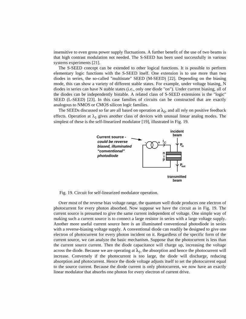
The SEEDs discussed so far are all based on operation at O0, and all rely on positive feedbackeffects. Operation at O� gives another class of devices with unusual linear analog modes. Thesimplest of these is the self-linearized modulator [19], illustrated in Fig. 19.
nip
+- I CPin
Pout
incidentbeam
transmittedbeam
Current source -could be reversebiased, illuminated“conventional”photodiode
Fig. 19. Circuit for self-linearized modulator operation.
Over most of the reverse bias voltage range, the quantum well diode produces one electron ofphotocurrent for every photon absorbed. Now suppose we have the circuit as in Fig. 19. Thecurrent source is presumed to give the same current independent of voltage. One simple way ofmaking such a current source is to connect a large resistor in series with a large voltage supply.Another more useful current source here is an illuminated conventional photodiode in serieswith a reverse-biasing voltage supply. A conventional diode can readily be designed to give oneelectron of photocurrent for every photon incident on it. Regardless of the specific form of thecurrent source, we can analyze the basic mechanism. Suppose that the photocurrent is less thanthe current source current. Then the diode capacitance will charge up, increasing the voltageacross the diode. Because we are operating at O1, the absorption and hence the photocurrent willincrease. Conversely if the photocurrent is too large, the diode will discharge, reducingabsorption and photocurrent. Hence the diode voltage adjusts itself to set the photocurrent equalto the source current. Because the diode current is only photocurrent, we now have an exactlylinear modulator that absorbs one photon for every electron of current drive.

S G D
n
i (quantum wells)
p (mirror)
photodiode
field-effect transistor
modulator
Fig. 20. Concept of the field-effect transistor SEED (FET-SEED). S - source; G - gate; D- drain.
When using the conventional photodiode as the current source, such a circuit can thereforegive a linear light-by-light modulator. An interesting recent extension is to differential circuits[24] that can perform image differentiation, subtraction, multiplication, and other analogfunctions.
Quantum well diodes, operating as both photodetectors and modulators, can also beintegrated with transistors. There are at least two reasons to do such integration. One problemfound in systems experiments with S-SEED devices is that, although they are relatively lowenergy switching devices by optical standards, they need too much optical power to allow large,fast systems to be built using present laser technology. Using transistors for electronic gainallows the optical energy requirements to be reduced. A second reason is that electronics is verygood at performing complex logic functions, at least locally. Combining electronics with theabilities of optics for interconnection may allow the best of both worlds. Indeed there are manyadvantages of optics for interconnection that become apparent once a good integrationtechnology is available (see, e.g., ref. [25]).
Fig. 20 shows the concept of one integration, the field-effect transistor SEED (FET-SEED)[26]. Here a quantum well diode is grown on top of a mirror as usual, in this case with the n-layer at the top. Then field effect transistors can be fabricated in the top layer. Hence thisconcept allows photodetectors for optical inputs, transistors for gain and logic, and quantumwell modulators for optical outputs.
Fig. 21 shows the actual layer structure for some current circuits [27]. The present state of theart in this technology is that, in the laboratory, small circuits have been operated with 22 fJ inputoptical energy, and at speeds up to 650 Mb/s. In actual multistage systems, larger "smart pixels"are operating with 100 fJ optical input energy at 155 Mb/s. A smart pixel array with 96 opticalbeams and 400 transistors was used in this system [28]. Such operating energies and speeds areof serious interest. For example, with 100 fJ input energy and a factor of 10 loss overall in anoptical system, a 1 W laser has sufficient power to drive 1 Tb/s of information through a system.This is a very large data rate, and one that is difficult to achieve with purely electronic systems

for a number of reasons (mostly related fundamentally to the skin effect and Maxwell'sequations).
GaAs 90 Å
AlGaAs 35 Åx95
n channel (AlGaAs spacer + 100 Å doped GaAs)
p+ conducting layer
H+ isolationimplant
Be p+implant
MQW region (1.2 Pm)
AlAs / AlGaAs dielectricreflector stack (2 Pm)
Semi-insulating GaAs substrate
n+ layer
AR coateddetector / modulator
diodeisolation drain
gate
sourceinterconnect
metal
Fig. 21 FET-SEED layer structure and cross-section.
Another approach to such integration is to combine quantum well devices with siliconelectronics. There has been success in monolithic integration of quantum well diodes ontosilicon [29], and it seems likely that various other hybrid schemes might also be possible
7. Conclusions
The optical properties of quantum wells near to the optical band-gap energy have proved to be afascinating laboratory for studying many novel physical mechanisms. In addition, several noveland practical devices have resulted that offer significantly new opportunities for optoelectronicsystems. We can expect continued evolution of physics, devices, and novel informationprocessing systems in the years to come.
Further Reading
For an introductory summary of quantum well optical physics and devices, seeD. A. B. Miller, "Optoelectronic applications of quantum wells", Optics and Photonics
News 1, No. 2, pp 7-15, February 1990.For a longer treatment of the physics, see
D. A. B. Miller, D. S. Chemla, and S. Schmitt-Rink, "Electric Field Dependence ofOptical Properties of Semiconductor Quantum Wells: Physics and Applications", andD. S. Chemla, S. Schmitt-Rink, and D. A. B. Miller, "Nonlinear Optical Properties ofSemiconductor Quantum Wells", both chapters in "Optical Nonlinearities andInstabilities in Semiconductors", ed. H. Haug, (Academic Press, Boston, 1988)

For an extensive discussion of quantum well optical physics seeS. Schmitt-Rink, D. S. Chemla, and D. A. B. Miller, "Linear and nonlinear optical
properties of semiconductor quantum wells", Advances in Physics 38, 89-188 (1989)For an extended discussion of band structure and states in quantum wells, see
G. Bastard, "Wave mechanics applied to semiconductor heterostructures", (Les Editionsde Physique, Les Ulis, France)
For extended treatments of quantum well optoelectronic devices seeD. A. B. Miller, "Quantum Well Optoelectronic Switching Devices", International
Journal of High Speed Electronics 1, 19-46 (1990)D. A. B. Miller, "Quantum Well Self Electrooptic-Effect Devices", Optical and Quantum
Electronics 22, S61-S98 (1990).
References
[1] see, e.g., A. Y. Cho, "Advances in molecular beam epitaxy (MBE)", Journal ofCrystal Growth 111, 1-13 (1991)
[2] see, e.g., K. Furuya, and Y. Miyamoto, "GaInAsP/InP organometallic vapor phaseepitaxy for research and fabrication of devices", Int. J. High Speed Electronics 1, 347-67 (1990)
[3] see, e.g., W. T. Tsang, "Progress in chemical beam epitaxy", J. Crystal Growth 105,1-29 (1990)
[4] For a recent discussion of envelope function models, including discussion of theboundary conditions, see M. G. Burt, "The justification for applying the effective-mass approximation to microstructures", J. Phys: Condens. Matter 4, 6651-6690(1992)
[5] see, e.g., C. Weisbuch, "Fundamental properties of III-V semiconductor two-dimensional quantized structures: the basis for optical and electronic deviceapplications", in “Semiconductors and Semimetals”, vol. 24, ed. R. Dingle (AcademicPress, New York, 1987), pp 1 - 117
[6] D. S. Chemla, D. A. B. Miller, P. W. Smith, A. C. Gossard, And W. Wiegmann,"Room temperature excitonic nonlinear absorption and refraction in GaAs/AlGaAsmultiple quantum well structures", IEEE J. Quantum Electron. 20, 265-275 (1984)
[7] S. Schmitt-Rink, D. S. Chemla, and D. A. B. Miller, "Theory of transient excitonicoptical nonlinearities in semiconductor quantum-well structures", Phys. Rev. B 326601-6609 (1985)
[8] P. W. Smith, Y. Silberberg, and D. A. B. Miller, "Mode locking of semiconductordiode lasers using saturable excitonic nonlinearities, J. Opt. Soc. Am. B2, 1228-1236(1985); Y. K. Chen, M. C. Wu, T. Tanbun-Ek, R. A. Logan, and M. A. Chin,"Subpicosecond monolithic colliding-pulse mode-locked multiple quantum welllasers", Appl. Phys. Lett. 58, 1253-1255 (1991); U. Keller, G. W. 't Hooft, W. H.Knox, and J. E. Cunningham, "Femtosecond pulses from a continuously self-startingpassively mode-locked Ti:sapphire laser", Optics Lett. 16, 1022-1024 (1991)
[9] D. A. B. Miller, D. S. Chemla, T. C. Damen, A. C. Gossard, W. Wiegmann, T. H.Wood, and C. A. Burrus, "Electric field dependence of optical absorption near thebandgap of quantum well structures", Phys. Rev. B 32, 1043-1060 (1985)

[10] D. A. B. Miller, J. S. Weiner, and D. S. Chemla, "Electric-field dependence of linearoptical properties of quantum well structures: waveguide electroabsorption and sumrules", IEEE J. Quantum Electron. QE-22, 1816-1830 (1986)
[11] G. D. Boyd, D. A. B. Miller, D. S. Chemla, S. L. McCall, A. C. Gossard, and J. H.English, "Multiple quantum well reflection modulator", Appl. Phys. Lett. 50, 1119-1121 (1987)
[12] see, e.g., M. Whitehead, A. Rivers, G. Parry, and J. S. Roberts, "A very low voltage,normally-off asymmetric Fabry-Perot reflection modulator", Electronics Lett. 26,1588-1590 (1990)
[13] A. M. Fox, D. A. B. Miller, G. Livescu, J. E. Cunningham, and W. Y. Jan,"Quantum well carrier sweep out: relation to electroabsorption and excitonsaturation", IEEE J. Quantum Electron. 27, 2281-2295 (1991)
[14] J. A. Cavaillès, D. A. B. Miller, J. E. Cunningham, P. Li Kam Wa, and A. Miller,"Simultaneous measurements of electron and hole sweep-out from quantum wells andmodeling of photoinduced field screening dynamics", IEEE J. Quantum Electron. 28,2486-2497 (1992)
[15] G. D. Boyd, J. A. Cavaillès, L. M. F. Chirovsky, and D. A. B. Miller, "Wavelengthdependence of saturation and thermal effects in multiple quantum well modulators",Appl. Phys. Lett. 63, 1715 - 1717 (1993)
[16] J. S. Weiner, D. A. B. Miller, and D. S. Chemla, "Quadratic electro-optic effect dueto the quantum-confined Stark effect in quantum wells", Appl. Phys. Lett. 50, 842-844(1987)
[17] J. E. Zucker, K. L. Jones, M. G. Young, B. I. Miller, and U. Koren, "Compactdirectional coupler switches using quantum well electrorefraction", Appl. Phys. Lett.55, 2280-2282 (1989)
[18] D. A. B. Miller, D. S. Chemla, T. C. Damen, T. H. Wood, C. A. Burrus, A. C.Gossard, and W. Wiegmann, "The quantum well self-electrooptic effect device:optoelectronic bistability and oscillation, and self linearized modulation", IEEE J.Quantum Electron. QE-21, 1462-1476 (1985)
[19] D. A. B. Miller, "Quantum-well self-electrooptic effect devices", Optical andQuantum Electron. 22, S61-S98 (1990)
[20] A. L. Lentine, H. S. Hinton, D. A. B. Miller, J. E. Henry, J. E. Cunningham, and L.M. F. Chirovsky, "Symmetric self-electrooptic effect device: optical set-reset latch,differential logic gate, and differential modulator/detector", IEEE J. QuantumElectron. 25, 1928-1936 (1989)
[21] M. E. Prise, "Optical computing using self-electro-optic effect devices" in "DigitalOptical Computing", ed. R. A. Athale, SPIE Critical Reviews of Optical Science andTechnology, CR35, 3-27 (1990); M. E. Prise et al., "Optical digital processor usingarrays of symmetric self-electro-optic-effect devices", Appl. Optics, 30, 2287-2296(1991); H. S. Hinton and D. A. B. Miller, "Free-Space Photonics in Switching",AT&T Technical Journal, 71, No. 1 (Jan/Feb), 84-92 (1992); F. B. McCormick, T. J.Cloonan, F. A. P. Tooley, A. L. Lentine, J. M. Sasian, J. L. Brubaker, R. L. Morrison,S. L. Walker, R. J. Crisci, R. A. Novotny, S. J. Hinterlong, H. S. Hinton, and E.Kerbis, "Six-stage digital free-space optical switching network using symmetric self-electro-optic-effect devices", Appl. Optics 32, 5153-5171 (1993).
[22] A. L. Lentine, D. A. B. Miller, J. E. Henry, J. E. Cunningham, and L. M. F.Chirovsky, "Multistate self-electrooptic effect devices", IEEE J. Quantum Electron.25, 1921-1927 (1989)
[23] A. L. Lentine, D. A. B. Miller, J. E. Henry, J. E. Cunningham, L. M. F. Chirovsky,and L. A. D'Asaro, "Optical logic using electrically connected quantum well PINdiode modulators and detectors", Appl. Optics 29, 2153-2163 (1990)
[24] D. A. B. Miller, "Novel analog self-electrooptic-effect devices", IEEE J. QuantumElectron. 29, 678-698 (1993); E. A. de Souza, L. Carraresi, G. D. Boyd, and D. A. B.Miller, "Analog differential self-linearized quantum-well self-electro-optic-effectmodulator", Optics Lett. 18, 974-976 (1993)
[25] D. A. B. Miller, "Optics for low-energy communication inside digital processors:quantum detectors, sources, and modulators as efficient impedance converters",Optics Lett. 14, 146-148 (1989)
[26] D. A. B. Miller, M. D. Feuer, T. Y. Chang, S. C. Shunk, J. E. Henry, D. J. Burrows,and D. S. Chemla, "Field-effect transistor self-electrooptic effect device: integratedphotodiode, quantum well modulator and transistor", IEEE Phot. Tech. Lett. 1, 61-64(1989)
[27] L. A. D'Asaro, L. M. F. Chirovsky, E. J. Laskowski, S. S. Pei, T. K. Woodward, A.L. Lentine, R. E. Leibenguth, J. W. Focht, J. M. Freund, G. G. Guth, and L. E. Smith,"Batch fabrication and operation of GaAs-AlGaAs field-effect transistor-self-electrooptic effect device (FET-SEED) smart pixel arrays", IEEE J. QuantumElectron. 29, 670-677 (1993)
[28] A. L. Lentine, F. B. McCormick, T. J. Cloonan, J. M. Sasian, R. L. Morrison, M. G.Beckman, S. L. Walker, M. J. Wojcik, S. J. Hinterlong, R. J. Crisci, R. A. Novotny,and H. S. Hinton, "A five stage free-space switching network using arrays of FET-SEED switching nodes", Conference on Lasers and Electrooptics, May 2-7, 1993,Baltimore, Maryland, Postdeadline Paper CPD24 (Optical Society of America, 1993)
[29] K. W. Goossen, G. D. Boyd, J. E. Cunningham, W. Y. Jan, D. A. B. Miller, D. S.Chemla, and R. M. Lum, "GaAs-AlGaAs multiquantum well reflection modulatorsgrown on GaAs and silicon substrates", IEEE Photonics Tech. Lett. 1, 304-306 (1989)