Quantum modelling of semiconductor gain materials and ... · PACS 42.55.Px, 42.60.Lh, 78.20.Bh, ......
20
physica status solidi, 7 December 2009 Quantum modelling of semiconductor gain materials and vertical-external-cavity surface-emitting laser systems Christina B ¨ uckers *,1 , Eckhard K¨ uhn 1 , Christoph Schlichenmaier 1 , Sebastian Imhof 2 , Angela Thr¨ anhardt 2 , J¨ org Hader 3,4 , Jerome V. Moloney 3,4 , Oleg Rubel 5,6 , Wei Zhang 7 , Thorsten Ackemann 8 , and Stephan W. Koch 1 1 Department of Physics and Material Sciences Center, Philipps-University Marburg, Renthof 5, 35032 Marburg, Germany 2 Faculty of Natural Sciences, Chemnitz University of Technology, 09107 Chemnitz, Germany 3 Nonlinear Control Strategies Inc., 3542 N. Geronimo Ave., Tucson, AZ 85705, USA 4 College of Optical Sciences, University of Arizona, Tucson, AZ 85721, USA 5 Thunder Bay Regional Research Institute, Thunder Bay, ON P7A 7T1, Canada 6 Department of Physics, Lakehead University, Thunder Bay, ON P7B 5E1, Canada 7 Centre for Biophotonics, SIPBS, University of Strathclyde, Glasgow G4 0NR, Scotland, UK 8 SUPA and Department of Physics, University of Strathclyde, Glasgow G4 0NG, Scotland, UK Received XXXX, revised XXXX, accepted XXXX Published online XXXX PACS 42.55.Px, 42.60.Lh, 78.20.Bh, 78.55.Cr, 85.35.Be ∗ Corresponding author: e-mail [email protected] This article gives an overview of the microscopic the- ory used to quantitatively model a wide range of semi- conductor laser gain materials. As a snapshot of the cur- rent state of research, applications to a variety of actual quantum-well systems are presented. Detailed theory- experiment comparisons are shown and it is analysed how the theory can be used to extract poorly known ma- terial parameters. The intrinsic laser loss processes due to radiative and non-radiative Auger recombination are evaluated microscopically. The results are used for realistic simulations of vertical- external-cavity surface-emitting laser systems. To ac- count for nonequilibrium effects, a simplified model is presented using pre-computed microscopic scatter- ing and dephasing rates. Prominent deviations from quasi-equilibrium carrier distributions are obtained un- der strong in-well pumping conditions. Copyright line will be provided by the publisher 1 Introduction The quantitative modelling of semi- conductor laser materials and their electronic excitations is of significant importance for the design and development of efficient and optimised semiconductor laser devices. The accurate description of the important system ingredients is particularly critical in modern microlasers, where the properties of the relatively small amount of gain material has to be well adapted to the specific microcavity. Exam- ples of current interest are vertical-external-cavity surface- emitting laser (VECSEL) systems also known as optically- pumped semiconductor disk lasers, which have recently emerged as a new class of semiconductor lasers [1–5]. They combine the advantages of a semiconductor gain medium with the solid-state-laser cavity design and allow for the extraction of a high-power, diffraction-limited cir- cular output beam [6, 7]. In the past decade, we have developed a many-particle theory to model the optical properties of semiconduc- tor quantum-well structures which are the basic building blocks in common semiconductor lasers [8,9]. By means of systematically derived microscopic equations, we quan- titatively predict the absorption, gain, refractive index, lu- minescence and the intrinsic laser losses of a system in a consistent way including microscopic interaction effects Copyright line will be provided by the publisher
Transcript of Quantum modelling of semiconductor gain materials and ... · PACS 42.55.Px, 42.60.Lh, 78.20.Bh, ......

physica status solidi, 7 December 2009
Quantum modelling ofsemiconductor gain materialsand vertical-external-cavitysurface-emitting laser systems
Christina Buckers*,1, Eckhard Kuhn1, Christoph Schlichenmaier1, Sebastian Imhof2, Angela Thranhardt2,Jorg Hader3,4, Jerome V. Moloney3,4, Oleg Rubel5,6, Wei Zhang7, Thorsten Ackemann8, and Stephan W. Koch1
1 Department of Physics and Material Sciences Center, Philipps-University Marburg, Renthof 5, 35032 Marburg, Germany2 Faculty of Natural Sciences, Chemnitz University of Technology, 09107 Chemnitz, Germany3 Nonlinear Control Strategies Inc., 3542 N. Geronimo Ave., Tucson, AZ 85705, USA4 College of Optical Sciences, University of Arizona, Tucson, AZ 85721, USA5 Thunder Bay Regional Research Institute, Thunder Bay, ON P7A 7T1, Canada6 Department of Physics, Lakehead University, Thunder Bay, ON P7B 5E1, Canada7 Centre for Biophotonics, SIPBS, University of Strathclyde, Glasgow G4 0NR, Scotland, UK8 SUPA and Department of Physics, University of Strathclyde, Glasgow G4 0NG, Scotland, UK
Received XXXX, revised XXXX, accepted XXXXPublished online XXXX
PACS 42.55.Px, 42.60.Lh, 78.20.Bh, 78.55.Cr, 85.35.Be
∗ Corresponding author: e-mail [email protected]
This article gives an overview of the microscopic the-ory used to quantitatively model a wide range of semi-conductor laser gain materials. As a snapshot of the cur-rent state of research, applications to a variety of actualquantum-well systems are presented. Detailed theory-experiment comparisons are shown and it is analysedhow the theory can be used to extract poorly known ma-terial parameters. The intrinsic laser loss processes dueto radiative and non-radiative Auger recombination areevaluated microscopically.
The results are used for realistic simulations of vertical-external-cavity surface-emitting laser systems. To ac-count for nonequilibrium effects, a simplified modelis presented using pre-computed microscopic scatter-ing and dephasing rates. Prominent deviations fromquasi-equilibrium carrier distributions are obtained un-der strong in-well pumping conditions.
Copyright line will be provided by the publisher
1 Introduction The quantitative modelling of semi-conductor laser materials and their electronic excitationsis of significant importance for the design and developmentof efficient and optimised semiconductor laser devices. Theaccurate description of the important system ingredientsis particularly critical in modern microlasers, where theproperties of the relatively small amount of gain materialhas to be well adapted to the specific microcavity. Exam-ples of current interest are vertical-external-cavity surface-emitting laser (VECSEL) systems also known as optically-pumped semiconductor disk lasers, which have recentlyemerged as a new class of semiconductor lasers [1–5].
They combine the advantages of a semiconductor gainmedium with the solid-state-laser cavity design and allowfor the extraction of a high-power, diffraction-limited cir-cular output beam [6,7].
In the past decade, we have developed a many-particletheory to model the optical properties of semiconduc-tor quantum-well structures which are the basic buildingblocks in common semiconductor lasers [8,9]. By meansof systematically derived microscopic equations, we quan-titatively predict the absorption, gain, refractive index, lu-minescence and the intrinsic laser losses of a system ina consistent way including microscopic interaction effects
Copyright line will be provided by the publisher

2 C. Buckers et al.: Quantum modelling of semiconductor gain materials and VECSEL systems
explicitly. The predictive capability of our model has beenvalidated by experiments for various material systems withemission wavelengths from the ultraviolet and visible tothe near- and mid-infrared, see e.g. [10–12].
The microscopically calculated optical properties ofsemiconductor gain materials may be used to analyse anddesign laser devices. Especially, in microcavity lasers theproper description of the intricate interplay of the cavityand the optical response of the active layers is essential.Employing the microscopic approach, main characteristicsof the laser device such as emission wavelength, thresh-old behaviour or input-output power characteristics can beevaluated.
This article reviews the application of the microscopicmodel to a wide range of material systems used in VEC-SEL and other laser systems. After our theoretical ap-proach is briefly introduced (Section 2), we discuss someof the relevant properties of an (AlGaIn)As-based VEC-SEL system in Section 3. Emphasis is placed on the anal-ysis of the lasing performance and in particular, the po-tential and limitations of optical in-well pumping are as-sessed. In Section 4 the laser gain and loss properties ofthe (AlGaInAs)(AsSb)-based material family are investi-gated and the application potential of various designs isexplored. Section 5 addresses the characterisation, the las-ing properties and disorder effects in the dilute nitride(GaIn)(NAs)-based material system. Furthermore, the suit-ability of our approach to extract critical structural param-eters through the analysis of spectroscopic measurementsis demonstrated in Section 6 for a Ga(AsSb)-based system.Finally, nonequilibrium effects are discussed in Section 7highlighting the impact of the pumping concept on the per-formance of VECSEL systems.
2 Theoretical approach Semiconductor laser de-vices are critically influenced by the optical response ofthe gain material so that any quantitative model requires aconsistent quantum mechanical theory. For this purpose,we have developed a microscopic model enabling us tosimulate the relevant electro-optical properties of semicon-ductor heterostructures in a consistent way. As the cen-tral part, the many-particle interactions are calculated ex-plicitly. Only the structural layout and material constantsare needed as input, and we do not have to resort to phe-nomenological parameters such as dephasing and scatter-ing rates, linewidth enhancement factors and the like.
The starting point of our approach is the calculationof the single-particle bandstructure and the correspond-ing Coulomb and dipole matrix elements. These are usedas input for the microscopic determination of the absorp-tion/gain, the photoluminescence, and the intrinsic laserloss processes. While absorption and photoluminescenceinvestigations allow for an accurate characterisation ofsemiconductor heterostructures, the laser gain and lossproperties are relevant ingredients for the final perfor-mance of the laser device.
2.1 Bandstructure For the computation of thesingle-particle eigenenergies and eigenstates in a semi-conductor heterostructure, we apply k·p-theory which isbased on a perturbation method [13]. If we consider III-Vsemiconductors such as (AlGaIn)As- or (AlGaIn)(AsSb)-based materials, the eigenstates of the quantum well maybe developed in split-off, heavy hole, light hole and elec-tronic contributions, each spin degenerated. In this man-ner, the band structure information is contained in an 8×8matrix, the so-called Luttinger matrix. However, for di-lute nitride (GaIn)(NAs)-based structures the matrix has tobe extended to a 10×10 matrix (Section 5). The requiredmaterial parameters for the bandstructure calculation aretaken from the literature [14,15]. Finally, from the single-particle wavefunctions, we determine the optical dipoleand Coulomb matrix elements needed for the microscopiccomputations.
2.2 Absorption and laser gain In order to computethe absorption/gain, the semiconductor Bloch equationsare solved in second Born-Markov approximation [16].The equations describe the dynamics of the microscopicpolarisations, i.e. the interband coherence at a certain mo-mentum, which couple to carrier densities present in thesystem. In most of our applications, the carriers can be as-sumed to be in quasi-equilibrium and thus in a Fermi-Diracdistribution. However, the general approach also allows usto study the impact of nonequilibrium situations which areaddressed in Section 7. Summing up the microscopic quan-tities yields the macroscopic polarisation which gives thelinear response of the material system to a light field.
In this manner, the refractive index change as wellas the absorption/gain spectrum of a quantum well canbe deduced. Since we calculate the many-particle corre-lations explicitly in second Born-Markov approximation,the homogeneous linewidth of the optical spectra is de-termined by quantum mechanical scattering equations in-cluding temperature, density, and spectral dependencies ina consistent way. Thus, phenomenological dephasing pa-rameters are not required and unphysical features such asabsorption below the band gap, wrong amplitudes and in-correct line shapes are avoided [17]. Our microscopic ap-proach has proven to realistically simulate the optical prop-erties through many comparisons to experiments for a mul-titude of material systems, see e.g. [18].
In laser systems such as VECSEL devices the semicon-ductor quantum wells are usually embedded in a micro-cavity. In order take the dielectric environment into con-sideration, we employ the transfer matrix method whichis a formalism accounting for the partial light reflectanceand transmission through a structure containing several in-terfaces [19]. In the transfer matrix, we include the op-tical response of the active layers by adding the absorp-tion/gain and the carrier-induced refractive index changesto the background refractive index of the quantum well lay-ers.
Copyright line will be provided by the publisher

pss header will be provided by the publisher 3
2.3 Photoluminescence Spontaneous emissionrates are calculated on the basis of the semiconductorluminescence equations [19], which include the equationsof motion for the photon number in a given light modeand the photon-assisted polarisations. They have beenderived similarly to the semiconductor Bloch equations,but involve the quantisation of the light field. As forthe computation of the absorption/gain, it is essential tocalculate the many-particle interactions explicitly sinceonly the inclusion of the excitonic correlations ensures thecorrect line shape of the resulting luminescence spectrumof the quantum-well system.
If one wants to compare calculated and experimentallymeasured spectra of a VECSEL system, one has to takeinto account that the line shape of a photoluminescencespectrum detected at the surface of a VECSEL structureis modified by cavity effects. In order to account for thedielectric environment in such weak-coupling systems, weapply an approach based on the derivation of a filter func-tion [20] which leads to the enhancement or reduction ofthe luminescence at certain wavelengths. If we multiply thefilter function evaluated for the specific dielectric structurewith the calculated emission spectrum of the isolated quan-tum well, we obtain the actually detected photolumines-cence at the surface of the structure.
2.4 Laser loss processes The performance of alaser device is influenced not only by the gain but alsoby the losses in the system. The material loss processesare typically classified into carrier recombination at de-fect states, spontaneous emission and Auger recombina-tion. The individual contributions of the various processesdepend on the particular material system and the operatingconditions such as temperature and carrier density. Often,the defect losses are negligible if one is dealing with high-quality materials. Hence, one is left with the radiative andAuger losses which we calculate microscopically.
The radiative loss rate is deduced by integrating pho-toluminescence spectra which are obtained by solving thesemiconductor luminescence equations. Furthermore, ourmicroscopic approach allows for the computation of thenon-radiative Auger recombination rates. For this purpose,we solve scattering equations for the electron and hole dis-tribution functions [9], which are derived in the same for-malism as the semiconductor Bloch and the semiconductorluminescence equations.
Phenomenologically, the spontaneous emission is ex-pected to increase quadratically with the carrier densitysince two particles participate in the process. Auger scatter-ing involves three particles, thus their contribution is sup-posed to increase cubically with carrier density. Althoughthis might be a good approximation below transparencywhen the carriers basically obey Boltzmann statistics, wefind strong deviations with increasing carrier density asdegenerate Fermi-Dirac distributions arise [9]. Thus, es-pecially in the density regime relevant for lasing in mostVECSEL systems the phenomenological formulas fail. In
contrast, the microscopic theory enables us to predict theradiative as well as the Auger losses quantitatively for anylasing condition [9,21].
Altogether, the microscopic evaluation of both the lasergain and the losses, supplemented by heat conduction andcavity waveguiding calculations allows for a systematicanalysis of semiconductor laser devices. Thus, the maincharacteristics of the system such as threshold behaviour,gain saturation or lasing wavelength can be studied and thepotential of the specific designs can be explored.
3 (AlGaIn)As-based VECSEL systems Well-established active materials for laser applications are(AlGaIn)As compounds. This material system is widelyused as a gain element in VECSEL devices. As a specificexample, we focus here on a design for a VECSELoperating at a wavelength around 850 nm [22–24].
Conventionally, the active material is pumped opticallyby an external laser diode via barrier states from which theexcited carriers relax into the quantum wells, thus generat-ing the occupation inversion [25]. An attractive alternativecould be the direct pumping of in-well states not only be-cause this would reduce the excess energy (quantum de-fect) of the photo-generated carriers, but also since thistechnique enhances the wavelength range of possible pumpsources, e.g. one could use bright and inexpensive diodesat 800-810nm [26].
In order to characterise and identify the relevant ingre-dients determining the performance of the VECSEL de-vice, we apply our systematic microscopic approach. Tofigure out design specifications of the structure, spectro-scopic measurements are analysed first.
3.1 Layout of the laser structure In a VECSEL de-vice light is amplified by semiconductor quantum wellswhich are embedded in a cavity built of a Bragg reflec-tor and an external outcoupling mirror which is aligned ata certain distance from the gain element. Here, we focuson a VECSEL structure intended to operate at an emissionwavelength around 850 nm.
The Bragg reflector is grown on a GaAs wafer using30 repeats of alternating AlAs and (Al0.18Ga0.82)As lay-ers which differ in their refractive indices as can be seenin the profile (Fig. 1, top). Each layer of the stack is de-signed to have the same optical thickness. Hence, a high-reflectivity stop-band centered at a wavelength of about836 nm with a width of about 84 nm for normal incidenceis established. On top of the Bragg reflector the active re-gion is deposited. It contains 17 (Al0.115Ga0.785In0.10)Asquantum wells which are 10 nm wide and are surroundedby barrier layers made of (Al0.26Ga0.74)As. The quantumwells are arranged to coincidence with the anti-nodes ofthe standing wave pattern of the laser mode (Fig. 1, bot-tom). Due to the huge spatial overlap of the active layerswith the light field maximal gain can be extracted. In be-tween quantum wells and barrier layers the sample con-tains (Al0.115Ga0.785In0.10)(As0.82P0.18) layers to reduce
Copyright line will be provided by the publisher

4 C. Buckers et al.: Quantum modelling of semiconductor gain materials and VECSEL systems
intensity of the propagating mode
gain region Bragg reflector buffer
z (μm)
refr
activ
e in
dex
0 2 4 60
1
2
3
4
5
z (μm)
refr
activ
e in
dex
1.0 1.2 1.40
2
4
Figure 1 Top: Refractive index profile of the VECSEL struc-ture at a temperature of 300 K (shaded area). The nominalstructure consists of a resonant periodic gain region with 17compressively strained (Al0.115Ga0.785In0.10)As quantum wellsembedded in (Al0.26Ga0.74)As barriers grown on a 30-pairAlAs / (Al0.18Ga0.82)As Bragg reflector. The quantum well posi-tions are indicated in darker grey. The curve represents the inten-sity of the light field at a wavelength of 850 nm along the struc-ture. Bottom: Refractive index profile and intensity distributionof the laser mode within the resonant periodic gain structure.
strain effects which are caused by the different lattice con-stant of the quantum well material compared to the otherlayers of the structure. However, the band gap of the quin-ternary material is almost equal to that of the barrier layer,thus in the microscopic calculations we assume the quan-tum wells to be sandwiched between (Al0.26Ga0.74)As forsimplicity. Finally, an (Al0.50Ga0.50)As window layer anda Ga(As0.90P0.10) protective capping layer close the struc-ture. Further details on design and growth of the sampleare given in [23].
All these different components in the structure lead tosteps in the refractive index profile which substantially af-fect the optical properties of the VECSEL. In particular, thelarge jump of the refractive index from air to the front sur-face of the sample shows much higher reflectance than thesemiconductor interfaces within the sample. Thus, a sub-cavity is formed between the sample surface and the frontof the Bragg reflector. The resonant periodic gain structuredefines a laser mode with a wavelength of about 850 nm,however this mode is not in resonance with the subcavityin the situation depicted in Fig. 1 because the mode ex-
hibits a node at the front surface of the sample reducingthe light coupling into the structure.
3.2 Optical characterisation The analysis of spec-troscopic measurements by the microscopic theory allowsfor a detailed characterisation of the VECSEL structure.For this purpose, reflectance as well as photoluminescenceinvestigations are carried out before building the laser cav-ity by aligning the external outcoupling mirror.
The reflectance spectrum of the sample measured atroom temperature for normal incidence is plotted in Fig. 2(dashed line). It is a result of interference effects of the lightpropagating and counter-propagating through the sample.In order to compute the reflectance and transmission at theboundaries of the dielectric structure, we employ the trans-fer matrix method. The required background refractive in-dices for the individual layers are extracted from the liter-ature [14,27,28] also taking into account the index disper-sion in the simulation. If we neglect the optical responseof the quantum wells to the light field as a start, we finda flat high reflectivity stop band with adjacent interferencefeatures next to it (Fig. 2, dash-dotted line).
For a realistic description of the VECSEL structure itis crucial to include the active layers in the simulation. Forthis purpose, we pre-compute the wavelength-dependentoptical susceptibility of the single quantum wells micro-scopically. The real part of the susceptibility determinesthe induced refractive index change in the quantum welllayer and the imaginary part gives the absorption withits characteristic excitonic peaks. These spectra repre-sent a critical input to the VECSEL design and are ob-tained by solving the semiconductor Bloch equations foran (Al0.108Ga0.785In0.107)As / (Al0.26Ga0.74)As quantumwell in the low-density regime. The spectra are convolutedwith a Gaussian distribution with a full width at half maxi-mum of 8 meV to account for growth inhomogeneities. Theincorporation of the microscopically computed spectra inthe transfer matrix calculation via wavelength-dependentcomplex refractive indices leads to a specific reduction ofthe reflectance at wavelengths where the quantum well ma-terial has absorption (Fig. 2, solid line). Due to the in-crease of intra-cavity losses in the excitonic resonances,two pronounced absorption dips arise in the stop-band at812 nm and 840 nm which match the experimental obser-vation (Fig. 2, dashed line). The 840 nm dip is caused bythe subcavity resonance coinciding with the excitonic res-onance induced by interband transitions between the firstelectron and the first hole subband.
The deviations of calculated and measured spectra out-side the stop-band may be attributed to slight uncertaintiesof the parameters assumed for the layer widths and the re-fractive indices. As the structure consists of more than 130layers, small changes of the individual structural parame-ters significantly affect the resulting reflectance, in partic-ular regarding the side slopes of the spectrum. However,the spectral range outside the stop-band is not relevant for
Copyright line will be provided by the publisher

pss header will be provided by the publisher 5
wavelength (nm)
refle
cted
inte
nsity
(%
)
750 800 850 875
0
50
100
150 experimentempty dielectric structurecoupling to QWs
Figure 2 Comparison of calculated (solid line) and measured(dashed line) reflectance spectrum of the VECSEL structure fornormal incidence at a temperature of 300 K. In the simulationmicroscopically calculated low-density absorption spectra for the(Al0.108Ga0.785In0.107)As / (Al0.26Ga0.74)As quantum wells areincluded. If the optical response of the quantum wells to the lightfield is not taken into account, the dash-dotted line will be ob-tained.
our current studies and thus no optimisation attempts havebeen made.
As another independent method to characterise theVECSEL structure, we investigate the photoluminescencefrom the surface of the sample. The solutions of the semi-conductor luminescence equations are shown in Fig. 3 asdash-dotted line. The main peak at 840 nm arises due totransitions between the first electron and the first hole sub-band. Furthermore, there is a second signal at 812 nm cor-responding to higher-order interband transitions. To ac-count for the dielectric environment of the cavity we eval-uate the filter function (Fig. 3, inset). The product of thisfilter function with the microscopically calculated photo-luminescence of the isolated quantum well yields the sur-face emitted photoluminescence spectrum (Fig. 3, solidline). The comparison shows that the photoluminescencesignals are more pronounced because of the spectral filter-ing. Both, the photoluminescence line shape as well as thespectral position agree well with the measurements (Fig. 3,dashed line).
3.3 Light amplification and laser loss propertiesAs soon as the VECSEL is pumped optically by an exter-nal laser diode, electrons are excited in the semiconductorstructure. They relax to lower energies and occupy statesnear the band edge of the quantum-well material wherethey alter the optical response.
The characteristic dependence of the absorption spec-trum on the carrier density is depicted in the insetof Fig. 4 (top) for a single (Al0.108Ga0.785In0.107)As /(Al0.26Ga0.74)As quantum well at a temperature of 300 K.Excitonic signatures corresponding to optically strong in-terband transitions brand the low-density spectrum, butwith increasing occupation the peaks bleach out and fi-
wavelength (nm)
norm
. pho
tolu
min
esce
nce
750 800 850 875
0
0.5
1
1.5 experimentisolated QWQWs in laser structure
wavelength (nm)
filte
r fu
nctio
n
800 825 8500
0.5
1
Figure 3 Comparison of calculated (solid line) and measured(dashed line) photoluminescence spectrum of the VECSEL struc-ture for normal incidence at a temperature of 300 K. In the sim-ulation cavity effects are taken into account by multiplying themicroscopically calculated luminescence spectrum of the sin-gle (Al0.108Ga0.785In0.107)As / (Al0.26Ga0.74)As quantum well(dash-dotted line) with the wavelength-dependent filter functionevaluated for the laser structure which is given in the inset.
nally, the absorption becomes negative in a spectral rangenear the band gap of the quantum well material and weenter the regime of optical gain.
The microscopic results enter the transfer matrix cal-culation yielding the light intensity actually reflected bythe VECSEL structure (Fig. 4, top). As soon as materialgain is provided at the position of the cavity resonance,a narrow peak arises at 843 nm superimposed on the stopband. The peak is slightly red shifted relative to the ab-sorption dip obtained for low pumping because the cou-pling strength to the adjacent cavity resonance is modified.Obviously, the reflectance becomes larger than 100 %, i.e.the light intensity will be amplified by the system aroundthe central wavelength. The amplification becomes moreand more enhanced with increasing excitation due to thegrowth of the maximum of the underlying material gainspectra. However, a higher carrier density not only leads toa larger material gain, but also broadens the material gainspectrally. At a carrier density of 5 × 1012 cm−2 per quan-tum well transparency is already exceeded for wavelengthsaround the next energetically higher cavity resonance sothat a second region of light amplification occurs around813 nm. However, with regard to laser operation only thecentral peak is relevant defining a lasing wavelength of843 nm at room temperature because this is the wavelengthfavored by the resonant periodic gain structure.
Experimentally, laser operation is observed at about850 nm. The red-shift relative to the theoretically predictedlasing wavelength of 843 nm can be attributed to heatingeffects in the active region. With increasing temperature,the cavity resonance shifts to longer wavelengths by anamount of about 0.1 nm per Kelvin, and the spectral re-gion providing material gain shifts even faster. If we carry
Copyright line will be provided by the publisher

6 C. Buckers et al.: Quantum modelling of semiconductor gain materials and VECSEL systems
out the calculations for a temperature of 350 K instead of300 K, lasing at 850 nm is expected matching the experi-mental finding (Fig. 4, bottom). So we conclude a temper-ature increase of about 50 K in the active region which isa typical value for operating VECSEL devices reported inthe literature [29].
The temperature increase results in a drop in amplifi-cation when the pumping power is kept constant. On theone hand, this trend is caused by the lower amplitude ofmaterial gain provided by the quantum wells as the carrierdistribution smears out energetically with increasing tem-perature. On the other hand, with growing temperature thematerial gain shifts faster to longer wavelengths than thecavity resonance. For a temperature of 350 K the overlapof gain and cavity resonance is already strongly reduced.That is why one needs higher excitation densities to sus-tain a certain amplification level when the operating tem-perature increases. At 350 K we find a carrier density of3.7 × 1012 cm−2 per quantum well required to achieve thelasing threshold of 5.3 % gain. This value is mainly deter-mined by the outcoupling losses, which are basically givenby the reflectivity of the external mirror used to completethe laser cavity, and the internal losses of the laser.
From the engineering point of view, it is not onlythe carrier density which is important but also the pumpintensity needed to sustain it. Hence it is crucial tostudy the loss processes in the semiconductor. Usingour many-particle theory, the loss rate due to sponta-neous emission and Auger recombination is evaluated foran (Al0.108Ga0.785In0.107)As / (Al0.26Ga0.74)As quantumwell (Fig. 5). From the analysis we conclude that Augerprocesses play a minor role in this particular system com-pared to the radiative losses for the entire carrier densityregime relevant for lasing. The recombination via defectsis negligible. Since the VECSEL is expected to operate atabout 350 K, the calculations are carried out for this tem-perature. Compared to the results obtained at room tem-perature, the total loss rate is reduced by more than oneorder of magnitude. It is true, that the Auger rate increaseswith temperature, but more important for this material sys-tem are the radiative losses which become considerablylower because the probability of spontaneous emission isreduced due to the broadened carrier distributions for thehigher temperature. However, the higher operating temper-ature also involves higher threshold carrier densities so thatthe benefits achieved by the reduced total laser losses aresuspended.
3.4 Analysis of in-well pumping From the quanti-tative knowledge of the absorption, gain, and laser lossproperties of the VECSEL structure the pump power nec-essary to achieve a certain amplification can be estimatedby equating the carrier generation rate needed to sustain thegain against recombination. As discussed in Section 3.3,a carrier density of 3.7×1012 cm−2 per quantum well isidentified to ensure an amplification of about 5.3 % repre-senting the threshold condition. For this threshold carrier
wavelength (nm)
refle
cted
inte
nsity
(%
)
700 750 800 850 900
0
50
100
150
wavelength (nm)
abso
rptio
n (c
m−
1 )
750 800 850 900
0
5000
10000
15000
experiment:5.3 % threshold@ 850 nm lasing
wavelength (nm)
refle
cted
inte
nsity
(%
)
800 850 900
80
100
120T = 300 KT = 325 KT = 350 K
Figure 4 Top: Reflectance of the VECSEL structure predictedat a temperature of 300 K for five different pumping levels.The underlying microscopically calculated absorption spectrafor the (Al0.108Ga0.785In0.107)As / (Al0.26Ga0.74)As quantumwell are displayed in the inset for carriers densities of 0.002,2, 3, 4 and 5 × 1012 cm−2 (from top to bottom). Bottom: Re-flectance of the VECSEL structure predicted at a carrier densityof 3.7 × 1012 cm−2 per quantum well for a temperature of 300 K(solid line), 325 K (dash-dotted line) and 350 K (dashed line). Inthe experiment, lasing at 850 nm has been observed.
density we find a loss rate of 2.7×10⁸ s−1 per quantumwell which includes radiative as well as Auger recombina-tion, see Fig. 5. As the loss rate has to be compensated bythe pumping, we demand
NQWRlossnthr =Ppump
hωpumpα(ωpump) (1)
where NQW is the number of quantum wells, R loss is thecarrier loss rate per quantum well, nthr is the threshold car-rier density, Ppump is the pump power per pumped area,hωpump is the energy of the pump light, and α(ωpump)gives the fraction of the pump radiation absorbed throughthe structure. The latter can be extracted from the calcu-lated reflectance and transmission spectra for the VECSELstructure and depends strongly on the pump wavelength,see Fig. 4.
Copyright line will be provided by the publisher

pss header will be provided by the publisher 7
carrier density (1012 cm−2)
loss
rat
e pe
r qu
antu
m w
ell (
s−1 )
2 4 6 8 10
106
107
108
109
spontaneous emissionAuger recombination
Figure 5 Laser losses due to spontaneous emission and Augerrecombination as a function of the carrier density for an(Al0.108Ga0.785In0.107)As / (Al0.26Ga0.74)As quantum well at atemperature of 350 K.
In this manner, we estimate the threshold pump poweras a function of the pump wavelength (Fig. 6). Obviouslythe efficiency of in-well pumping will drop rapidly if thepump wavelength is too close at the lasing wavelength. Assoon as the pump wavelength exceeds a value of 822 nm,the required pump power increases drastically. In this spec-tral region the absorption is bleached out already by theinduced generated carriers, thus limiting the pump wave-length.
The experimentally applied threshold pump intensity is4.5×108 W m−2 for a pump wavelength between 806 nmand 810 nm. This corresponds quite well to the theoreti-cal estimation. Differences could be caused by the fact thatonly parts of the pumped area contribute to lasing, thusthe experimental threshold pump power per area might belarger. Moreover, in the calculation we assume each quan-tum well to be excited with equal power, but the absorptionof the pump radiation might be rather inhomogeneous dueto the fact that the standing wave distribution of the pumpdoes not equal that of the laser and hence its anti-nodes arenot optimally overlapping with the quantum wells.
It is worth noting that it is essential for the analysis tohave the microscopic model allowing for quantitative pre-dictions of the optical properties of the gain element in theVECSEL device. Simpler models would lead to incorrectconclusions as the lasing performance depends substan-tially on the spectral position of the quantum well absorp-tion/gain, its amplitude, the line shape of the spectra as wellas the temperature and carrier density of all these quanti-ties. And besides, if the extracted threshold carrier densitywas incorrect, the error would be even further enhanced inthe determination of the laser loss processes which reactvery sensitively to the assumed carrier density. The many-particle approach has proven to simulate all these aspectsrealistically, thus allowing for an accurate characterisation.Hence, in particular the potential and limitations of optical
drastic increase of thepump power requiredto reach threshold
pump wavelength (nm)
pum
p po
wer
(10
9 W m
−2 )
740 760 780 800 820 8400
1
2
3
Figure 6 Pump power needed to sustain the threshold gain as afunction of the pump wavelength. For the evaluation a tempera-ture of 350 K is assumed in the active region.
in-well pumping for the 850 nm VECSEL could be anal-ysed with special emphasis on the bleaching of the pumpabsorption. One important consequence is that pump andlasing wavelength should be separated in this system by atleast 25 nm to sustain the necessary threshold gain. Thismeans, that 800-810nm diodes can pump the 850 nm lasersystem quite efficiently.
It is interesting to investigate whether other materialsystems and wavelength regions can benefit from in-wellpumping. For example, deep-blue and ultraviolet GaNdiodes might be used to pump blue-green VECSELs and670 nm diodes to drive VECSELs in the 700-750nm re-gion. Obviously, a microscopic theory as developed herewill be very helpful in assessing these situations.
4 (AlGaIn)(AsSb)-based lasers for long-wavelengths Semiconductor lasers emitting around2 μm are of considerable interest for a multitude ofapplications, such as medical diagnostics, material pro-cessing or spectroscopic trace gas detection. Based onthe (AlGaIn)(AsSb) material class various designs withemission wavelength from 1.8 μm up to 3 μm have beenpresented, including diode lasers as well as VECSELdevices [30–35].
In order to study the basic optical properties of a pos-sible material system in the long-wavelength regime, weanalyse the absorption/gain of a (GaIn)Sb quantum wellstructure emitting around 2 μm by means of our micro-scopic approach. Here, we use our quantitative theory todeduce experimentally not directly obtainable quantities,in particular band-structure details. Besides the laser gain,also the laser loss processes are studied with the goal toexplore the potential of different laser designs.
For emission wavelengths above 3 μm most conven-tional type-I quantum well structures are not useful anymore since high internal losses hamper their operation. Analternative concept to overcome these limitations are type-
Copyright line will be provided by the publisher

8 C. Buckers et al.: Quantum modelling of semiconductor gain materials and VECSEL systems
II “W” active regions [36]. Again, the physical processesaffecting the lasing parameters of such a device can beanalysed by our microscopic approach.
4.1 Analysis of the laser gain properties For thewavelength regime around 2 μm quantum well lasers em-ploying ternary (GaIn)Sb compounds are well suited.Based on the microscopic theory we analyse the materialproperties, in particular the optical gain, of such a (GaIn)Sblaser structure [12].
The GaSb-based diode laser we consider con-tains three 10 nm wide compressively strained(Ga0.78In0.22)Sb quantum wells which are sepa-rated by (Al0.30Ga0.70)(As0.02Sb0.98) barriers with athickness of 20 nm. The active region is surroundedby 400 nm wide layers on each side, also made of(Al0.30Ga0.70)(As0.02Sb0.98). These, in turn, are embed-ded in (Al0.84Ga0.16)(As0.06Sb0.94) cladding layers. Asthe cladding layers have a considerably lower refractiveindex according to the higher aluminium concentrationthere is a remarkable jump of the refractive index fromthe barrier to the cladding layer on each side and thus,an optical waveguide is formed enclosing the laser modein between. The overlap of the optical mode with theactive layers, i.e. the three quantum wells of the system,determines a confinement factor for the laser structureof about 6.6 %. Actually, the amplification of the lightmode through the system is given by the product of theconfinement factor and the material gain provided by asingle quantum well.
In order to study and analyse the gain properties ofthe laser structure, material gain spectra are computedbased on the semiconductor Bloch equations for variouscarrier densities assuming a disorder-induced inhomoge-neous broadening of 10 meV. Multiplying these spectrawith the confinement factor yields the modal gain of thelaser structure (Fig. 7, solid lines). In this manner, the cal-culations can be compared to experimental spectra. Here,we use gain for a 500μm long and 6 μm wide ridge waveg-uide laser at various excitation currents below thresholdemploying the method of Hakki and Paoli (Fig. 7, cir-cles). With growing excitation, the spectral width and am-plitude increase as well as the gain maximum becomesslightly blue-shifted. The spectral position of the gain peakmatches within growth uncertainties and the line shape isalso well reproduced.
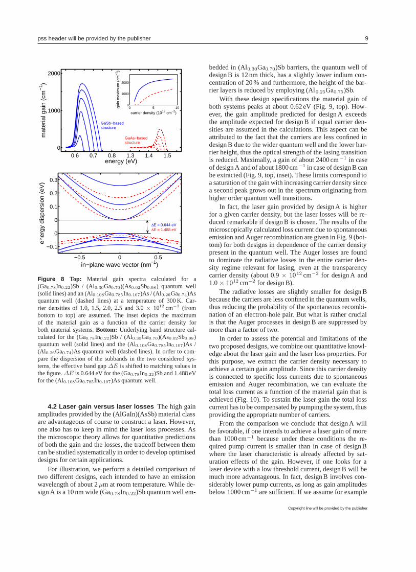
The gain provided by the material system has a re-markably large amplitude exceeding that of more com-mon GaAs-based structures. For illustration, in Fig. 8(top) material gain spectra of the (Ga0.78In0.22)Sb quan-tum well are shown and compared to spectra obtained forthe (Al0.115Ga0.785In0.10)As quantum well employed inthe VECSEL addressed in Section 3. Since the calculationassumes the same temperature and equal carrier densitiesin both cases, one clearly observes that the gain amplitudeis considerably higher in the (GaIn)Sb structure. The max-imal material gain which can be extracted is almost twice
energy (eV)
mod
al g
ain
(cm
−1 )
0.62 0.63 0.64 0.65 0.66
−20
0
20
40
Figure 7 Comparison of calculated (solid lines) and mea-sured (circles) modal gain spectra in the (Ga0.78In0.22)Sb /(Al0.30Ga0.70)(As0.02Sb0.98) laser structure at a temperature of280 K for various excitations. In the simulation carrier densitiesof 0.65, 0.7, 0.75, 0.8, 0.85, 0.9, 0.95 and 1.0 × 1012 cm−2 (frombottom to top) are assumed. The spectra are shifted 4 meV to-ward higher energies which can be attributed to slight deviationsof the actual growth from the nominal design. The experimentalspectra are obtained employing the method of Hakki and Paolifor excitation currents of 12.7, 14.6, 16.9, 18.9, 20.8 and 22.8 mA(from bottom to top). The experiment was done by M. Rattunde,N. Schulz, and J. Wagner at the “Fraunhofer Institut fur Ange-wandte Festkorperphysik”. [12]
the value obtained for the GaAs-based structure (Fig. 8,top, inset).
The physical reasons for the beneficial gain propertiesof the GaSb-based material class are found in band struc-ture effects which are analysed through a detailed com-parison with the results for the GaAs-based system. Onthe one hand, the reduced band gap of (GaIn)Sb involvesan increased gain amplitude, which will be visible if oneperforms the calculations again taking the band gap en-ergy of the GaAs-based structure artificially at the value of(GaIn)Sb. On the other hand, the high gain in the (GaIn)Sbsystem is a result of an advantageous band dispersion(Fig. 8, bottom). The subbands of the GaSb-based structureare curved more strongly with the result that the effectivemasses are smaller compared to those of the GaAs-basedsystem and they are more similar to the hole masses. Sincethese features offer optimised conditions for a low trans-parency density and a high differential gain, the (GaIn)Sbsystem is more beneficial than the GaAs-based structurewith heavier and more differing electron and hole masses.Besides, the electron as well as the hole subbands are sepa-rated better in the (GaIn)Sb case, thus states in higher sub-bands are less occupied and the number of carriers in thestates contributing to the lasing transition increases for agiven carrier density and temperature. Consequently, thecombination of these band structure effects leads to the ex-cellent gain properties of the (GaIn)Sb material system.
Copyright line will be provided by the publisher
pss header will be provided by the publisher 9
GaSb−basedstructure
GaAs−basedstructure
energy (eV)
mat
eria
l gai
n (c
m−
1 )
0.6 0.7 0.8 1.3 1.4 1.50
1000
2000
carrier density (1012 cm−2)ga
in m
axim
um (
cm−
1 )
0 5 100
1000
2000
in−plane wave vector (nm−1)
ener
gy d
ispe
rsio
n (e
V)
ΔE = 0.644 eVΔE = 1.488 eV
−0.5 0 0.5
−0.1
0
0
0.1
0.2
0.3
Figure 8 Top: Material gain spectra calculated for a(Ga0.78In0.22)Sb / (Al0.30Ga0.70)(As0.02Sb0.98) quantum well(solid lines) and an (Al0.108Ga0.785In0.107)As / (Al0.26Ga0.74)Asquantum well (dashed lines) at a temperature of 300 K. Car-rier densities of 1.0, 1.5, 2.0, 2.5 and 3.0 × 1012 cm−2 (frombottom to top) are assumed. The inset depicts the maximumof the material gain as a function of the carrier density forboth material systems. Bottom: Underlying band structure cal-culated for the (Ga0.78In0.22)Sb / (Al0.30Ga0.70)(As0.02Sb0.98)quantum well (solid lines) and the (Al0.108Ga0.785In0.107)As /(Al0.26Ga0.74)As quantum well (dashed lines). In order to com-pare the dispersion of the subbands in the two considered sys-tems, the effective band gap ΔE is shifted to matching values inthe figure. ΔE is 0.644 eV for the (Ga0.78In0.22)Sb and 1.488 eVfor the (Al0.108Ga0.785In0.107)As quantum well.
4.2 Laser gain versus laser losses The high gainamplitudes provided by the (AlGaIn)(AsSb) material classare advantageous of course to construct a laser. However,one also has to keep in mind the laser loss processes. Asthe microscopic theory allows for quantitative predictionsof both the gain and the losses, the tradeoff between themcan be studied systematically in order to develop optimiseddesigns for certain applications.
For illustration, we perform a detailed comparison oftwo different designs, each intended to have an emissionwavelength of about 2 μm at room temperature. While de-sign A is a 10 nm wide (Ga0.78In0.22)Sb quantum well em-
bedded in (Al0.30Ga0.70)Sb barriers, the quantum well ofdesign B is 12 nm thick, has a slightly lower indium con-centration of 20 % and furthermore, the height of the bar-rier layers is reduced by employing (Al0.25Ga0.75)Sb.
With these design specifications the material gain ofboth systems peaks at about 0.62 eV (Fig. 9, top). How-ever, the gain amplitude predicted for design A exceedsthe amplitude expected for design B if equal carrier den-sities are assumed in the calculations. This aspect can beattributed to the fact that the carriers are less confined indesign B due to the wider quantum well and the lower bar-rier height, thus the optical strength of the lasing transitionis reduced. Maximally, a gain of about 2400 cm−1 in caseof design A and of about 1800cm−1 in case of design B canbe extracted (Fig. 9, top, inset). These limits correspond toa saturation of the gain with increasing carrier density sincea second peak grows out in the spectrum originating fromhigher order quantum well transitions.
In fact, the laser gain provided by design A is higherfor a given carrier density, but the laser losses will be re-duced remarkable if design B is chosen. The results of themicroscopically calculated loss current due to spontaneousemission and Auger recombination are given in Fig. 9 (bot-tom) for both designs in dependence of the carrier densitypresent in the quantum well. The Auger losses are foundto dominate the radiative losses in the entire carrier den-sity regime relevant for lasing, even at the transparencycarrier density (about 0.9 × 1012 cm−2 for design A and1.0 × 1012 cm−2 for design B).
The radiative losses are slightly smaller for design Bbecause the carriers are less confined in the quantum wells,thus reducing the probability of the spontaneous recombi-nation of an electron-hole pair. But what is rather crucialis that the Auger processes in design B are suppressed bymore than a factor of two.
In order to assess the potential and limitations of thetwo proposed designs, we combine our quantitative knowl-edge about the laser gain and the laser loss properties. Forthis purpose, we extract the carrier density necessary toachieve a certain gain amplitude. Since this carrier densityis connected to specific loss currents due to spontaneousemission and Auger recombination, we can evaluate thetotal loss current as a function of the material gain that isachieved (Fig. 10). To sustain the laser gain the total losscurrent has to be compensated by pumping the system, thusproviding the appropriate number of carriers.
From the comparison we conclude that design A willbe favorable, if one intends to achieve a laser gain of morethan 1000 cm−1 because under these conditions the re-quired pump current is smaller than in case of design Bwhere the laser characteristic is already affected by sat-uration effects of the gain. However, if one looks for alaser device with a low threshold current, design B will bemuch more advantageous. In fact, design B involves con-siderably lower pump currents, as long as gain amplitudesbelow 1000 cm−1 are sufficient. If we assume for example
Copyright line will be provided by the publisher

10 C. Buckers et al.: Quantum modelling of semiconductor gain materials and VECSEL systems
energy (eV)
mat
eria
l gai
n (c
m−
1 )
0.6 0.7 0.8 0.90
1000
2000
3000
design Adesign B
carrier density (1012 cm−2)
gain
max
imum
(cm
−1 )
0 5 100
1000
2000
spontaneousemission
Auger
carrier density (1012 cm−2)
loss
cur
rent
(A
cm
−2 )
0.5 1 2 4 810
0
101
102
103
104
105
design Adesign B
Figure 9 Top: Material gain spectra calculated for a 10 nmwide (Ga0.78In0.22)Sb / (Al0.30Ga0.70)Sb quantum well, denotedas design A (solid lines) and a 12 nm wide (Ga0.80In0.20)Sb /(Al0.25Ga0.75)Sb quantum well, denoted as design B (dashedlines) at a temperature of 300 K. Carrier densities of 1, 2, 3, 4and 5 × 1012 cm−2 (from bottom to top) are assumed. The insetdepicts the maximum of the material gain as a function of the car-rier density for both material systems. Bottom: Laser loss currentdue to spontaneous emission and Auger recombination as a func-tion of the carrier density for design A (solid lines) and design B(dashed lines) at a temperature of 300 K.
a threshold gain peak of 500 cm−1, a threshold current ofabout 125 A cm−2 has to be provided regarding design B.This amount is about 35 % smaller than the pump currentwhich has to be applied to design A to achieve the samegain amplitude.
It is worth noting that Auger losses are particularystrong in materials with narrow band gaps. Consideringthe (GaIn)Sb quantum well, the Auger processes domi-nate the spontaneous recombination even at transparencyand they increase drastically with growing carrier density(Fig. 9, bottom). In contrast, in Section 3 we investigate forinstance a GaAs-based (Al0.115Ga0.785In0.10)As quantumwell structure which has a band gap that is twice as largeas the band gap of (GaIn)Sb, and for this system the con-tribution of Auger recombination plays a minor role com-pared to the radiative losses (Fig. 5). Because of the par-
material gain (cm−1)
tota
l los
s cu
rren
t (A
cm
−2 )
100 200 400 800
102
103
design Adesign B
Figure 10 Laser loss current including radiative and Auger re-combination as a function of the material gain provided for de-sign A (solid line) and design B (dashed line) at a temperature of300 K.
ticular high Auger losses in the GaSb-based material sys-tem adequate designs are required to overcome these limi-tations. The comparison of design A and design B demon-strates that the potential of various structural layouts canbe studied systematically on the basis of the microscopicapproach. In this manner, structures with e.g. low thresh-old or high output power are found, so that laser devicescan be optimised with regard to applications.
4.3 Investigation of mid-infrared type-II “W“diode lasers The quantum-well structures presented inSection 4.1 and Section 4.2 are suitable for laser emissionat 2.X μm. However, if one aims for even longer emissionwavelengths in the mid-infrared, their operation will bestrong affected by high internal losses. To circumvent theselimitations alternative concepts have been considered, inparticular diode lasers with type-II “W” active regions arediscussed [36]. They fill the spectral range between 3 μmand 4 μm given by type-I quantum well lasers on the short-wavelength side and by quantum cascade lasers [37] onthe long-wavelength side. Based on the microscopic the-ory, we investigate the lasing properties of an antimonidetype-II “W” diode laser structure emitting at 3.4 μm [38].
The laser structure consists of five so-called “W”elements [39]. Each is formed by a 3 nm wide(Ga0.925In0.075)Sb hole quantum well which is sand-wiched between 2.16 nm thick InAs layers providing wellsfor the electrons. These layers are in turn embeddedin (Al0.53Ga0.47)Sb. Thus, a short type-II superlattice isformed where electrons and holes are localised in adjacentlayers (Fig. 11). Since electrons and holes are locally sep-arated in the type-II structure, the Auger coupling strengthis reduced so that the loss rate is smaller than in a type-I sit-uation where electrons and holes are confined in the samelayer. Obviously, the type-II design also involves reducedgain amplitudes, but what is rather crucial is the tradeoffbetween reduced losses and reduced gain.
Copyright line will be provided by the publisher

pss header will be provided by the publisher 11
z (nm)
-1
0
1
ener
gy (
eV)
1 5 10
Figure 11 Confinement potential for electrons (black, thick line)and heavy holes (gray, thick line) in the “W” element of thelaser structure, which is formed by a layer sequence of InAs /(Ga0.925In0.075)Sb / InAs / (Al0.53Ga0.47)Sb. The thinly plottedcurves indicate the lowest electron and the lowest hole confine-ment wave function respectively. The corresponding energy lev-els are marked as dashed lines.
By evaluating the laser gain and the laser losses mi-croscopically, we predict the threshold current of the laserdiode in a temperature range between 80 K and 300 K.The results are in quantitative agreement with the exper-iment and a considerable increase of the threshold currentwith growing temperature is observed [38]. Through themicroscopic analysis this behaviour can be attributed to athermally reduced gain amplitude which involves higherthreshold carrier densities and thus higher loss currents. Incontrast, the Auger coefficient is found to be nearly tem-perature independent.
5 (GaIn)(NAs)-based material system After firstreports of an increasing redshift of the band-edge lumi-nescence with increasing nitrogen content in 1992 [40],(GaIn)(NAs) has been under intense investigation for itspotential application as a GaAs-based laser material attelecommunication wavelengths. The most widely knownspecialty of (GaIn)(NAs) and related materials is the huge,composition-dependent bandgap bowing which also ac-counts for the unexpectedly small bandgap. The intri-cate band structure may be described by the anticrossingmodel [41–43] where the nitrogen atoms are identified withan impurity band interfering with the conduction band. Theresulting anticrossing pushes the conduction band edge tolower energies. In the formalism of k·p-theory, the anti-crossing model corresponds to an extension of the 8×8 toa 10×10 k·p-matrix.
5.1 Characterisation of (GaIn)(NAs) structuresIn order to use (GaIn)(NAs) material to its maximum po-tential, it has to be characterised thoroughly. However, be-ing a long wavelength material grown on GaAs, a numberof characterisation measurements are hampered by sub-strate absorption. Photomodulated reflectance [44–46] of-fers a possibility to sensitively measure optical spectra
1.15 1.2 1.25 1.3 1.35−20
−10
0
10
20
energy (eV)
PR &
abs
orpt
ion
(arb
. u.)
absorption
PR
PR
theory
exp
Figure 12 Calculated (solid line) and measured (dotted line) pho-tomodulated reflectance spectra at a temperature of 300 K for astructure consisting of 9.4 nm wide (In0.23Ga0.77)As quantumwells between 35 nm wide Ga(N0.0048As0.9952) barriers. The cal-culated absorption spectrum (dashed line) is vertically displacedfor clarity. Taken from [47].
without substrate interference. This enabled a study of thetype-I-type-II transition in a series of InGaAs-GaNxAs1−x
samples. Four samples with nitrogen contents x=0.48%,0.72%, 1.25%, and 2.2% were investigated [47].
Photomodulated reflectance experiments are per-formed by varying a modulation pump between zero and asmall value while measuring the change in reflectance withthe help of a probe beam. The microscopic simulation ofphotomodulated reflectance is not straightforward becausethe mechanism causing the reflectance change is largelyunknown. Our calculations were performed by determin-ing the difference between two spectra at slightly varyingdensities. It is widely assumed that the modulation signalis caused by a change in electric field in the sample due tolocal charge inhomogeneities. We model these effects bysolving Poisson’s equation but find the signals dominatedby the pump-induced density change rather than the elec-tric field.
Figure 12 shows a calculated absorption spec-trum (dashed line) for a series of three 9.4 nmwide (In0.23Ga0.77)As wells between 35 nm wideGa(N0.0048As0.9952) barriers and the correspondingcalculated photomodulated reflectance signal (solid line).For comparison, the experimental curve is also shown.Looking at the two theory curves for absorption and photo-modulated reflectance, we remark that the peak absorptionenergies are approximately given by the zero crossingsof the differential signal. The calculation reproduces themain features of the experiment even without any linefitting parameters. The only adjustable quantity is thedisorder-induced inhomogeneous broadening which wasset to 6.7 meV to model the experiment.
Figure 13 extends the theory-experiment comparison toinclude four samples with different nitrogen contents in thebarriers, x=0.48%, 0.72%, 1.25%, 2.2%. For all cases, themain features are clearly reproduced. Some transitions are
Copyright line will be provided by the publisher

12 C. Buckers et al.: Quantum modelling of semiconductor gain materials and VECSEL systems
1.1 1.15 1.2 1.25 1.3 1.350
10
20
30
40
50
60
70
energy (eV)
PR (a
rb. u
.)
x=0.48%
x=0.72%
x=1.25%
x=2.2%
Figure 13 Calculated (solid lines) and measured (dashed lines)photomodulated reflectance spectra for the four samples inves-tigated here. The nitrogen content in the barriers varies fromx=0.48%, 0.72%, 1.25%, to 2.2%. A type-I-type-II-transition canbe shown to occur between x=0.72% and x=1.25%. The spectraare vertically displaced for clarity. Taken from [47].
less pronounced in the experiment, probably due to sampleinhomogeneities. Regarding the lowest transition, we seeit move to lower energies and lose oscillator strength fromx=0.48% to x=0.72% and attribute this effect to the de-creasing electron confinement. For the x=1.25%-structurethe transition has vanished as a result of the type-I-type-II-transition with rising nitrogen content. In Ref. [47], thistransition was further illustrated using a combination of ex-perimental methods.
These spectra are an example of a wide range of exper-iments in (GaIn)(NAs) which can be modelled by micro-scopic theory. Further works in this area may be found inRef. [8,48,49].
5.2 Towards 1.55µm In recent years, the growth ofhigh quality (GaIn)(NAs) material emitting at a wave-length of 1.55μm has increasingly become attainable.Even though progress has been slow due to the high in-dium and nitrogen contents involved, relatively low thresh-old lasers beyond 1.55 μm have been demonstrated [50]. Amajor improvement in growth outcome may be achievedby the addition of antimony [51–55].
Our microscopic model allows us to consider the gainand loss properties of (GaIn)(NAs) in the entire 1.3–1.55μm range independent of any growth issues [56], ad-dressing the question whether the degrading of opticalproperties at higher wavelengths is an intrinsic or a ma-terial quality related phenomenon. Figure 14 shows theintensity gain at 1.3 μm (solid lines) and 1.55μm (dottedlines) in a quantum well structure containing 40 % indium.The nitrogen content was varied from 0.55% to 2.3% inorder to change the emission wavelength.
(GaIn)(NAs) being a quaternary material, differentcompositions may be used to achieve emission at a specificwavelength. Samples with different indium and nitrogencontents but emitting at the same wavelength are also com-
0
1
2
3
4
5
6
0.7 0.8 0.9 1 1.1
1.8 1.6 1.4 1.2 1.1
mat
eria
l gai
n (1
03 c
m-1)
energy (eV)
wavelength (μm)
Figure 14 Intensity gain at 1.3 μm (solid lines) and 1.55 μm (dot-ted lines) for a quantum well structure containing 40 % indium.The dashed and dash-dotted lines show the effect of differentstrain which may be achieved by varying both indium and nitro-gen content, but keeping the emission wavelength constant. Thedashed line corresponds to an unstrained sample. Obviously, thegain is much broader, and correspondingly the required carrierdensity is almost twice as high.
pared in Fig. 14. The dashed and dash-dotted lines showthe effect of different compositions at a constant emis-sion wavelength of 1.3μm. For instance, the dashed linecorresponds to an unstrained sample. Obviously, the gainis much broader, and correspondingly the required carrierdensity is almost twice as high as for the 40% indium struc-ture. To illustrate this dependence, we investigate two se-ries of materials:
A Constant indium: The indium content is kept at 40%,the wavelength is varied by changing the nitrogen con-tent.
B Constant strain: The strain is kept constant by varyingboth indium and nitrogen content.
Figure 15 shows the carrier density necessary to obtaina certain peak gain for the two material series at 1.3 μm and1.55μm. As discussed before, the density is lower for thehighly strained samples with 40% indium content (exx=-2.65% for 1.3μm, exx=-2.35% for 1.55μm). This is alsovisible in the inset which is a magnification of the largefigure for small gains.
Having access to the full information in our micro-scopic calculation, we can explain the effects in detail. Thedifferences in required density are due to the band structurewhere composition changes induce the following effects:
1.Increased energetic separation of nitrogen level andconduction band edge for increased nitrogen content
2.Decreased electron mass for reduced nitrogen contentand increased indium content
3.Split off of light holes due to compressive strain; higherstrain raises the heavy hole content of the confined sub-bands and reduces their effective mass
Copyright line will be provided by the publisher

pss header will be provided by the publisher 13
0
5
10
15
0 1 2 3 4 5carr
ier d
ensi
ty (1
012 c
m-2)
gain maximum (103 cm-1)
40%In1.55µm
40%In1.3µm
exx=-1%1.3µm
exx=-1%1.55µm
1
1.5
2
0 0.5 1
Figure 15 Carrier density necessary to obtain a certain peak gainfor the two material series at 1.3 μm and 1.55 μm. Thick lines: Se-ries A, 1.55 μm (dotted) and 1.3 μm structure (solid). Thin lines:Series B, 1.55 μm (dash-dotted) and 1.3 μm structure (dashed).The inset is a magnification of the large figure for small gains.
gain (103 cm-1)
loss
cur
rent
/ ga
in (A
cm-1)
0 1 2 3 40.3
1
10
Figure 16 Ratio of total loss current to peak gain. For themonomolecular loss, a monomolecular recombination time of1 ns is assumed.
Comparing series A and B in the light of the abovebandstructure dependencies, we remark that effect (2) and(3) lead to the observed higher gain for a given densityfor series A, while effect (1) weakens this phenomenon.In this quaternary material, one must thus strive to includeas much strain as possible while still maintaining a highmaterial quality.
Next, we microscopically calculate losses by Augerand spontaneous emission processes. Being a long wave-length material, Auger processes clearly dominate [56].In order to identify the gain region where the excitationof the quantum well is most efficiently turned into lightamplification, we divide the total loss current Jtot =Jmono + Jsp + Jaug by the peak gain. Here, Jmono, Jsp
and Jaug are loss currents by monomolecular, spontaneousand Auger recombination, respectively. The monomolecu-lar contribution is caused by non-radiative recombinationprocesses at defect states and thus, basically depends onthe quality of the material. The corresponding loss current
is given by Jmono = eτ−1ρ, where e is the unit charge,τ = 1 ns is a typical decay time in a (GaIn)(NAs) laser for1300 nm emission [57], and ρ is the carrier density. Theloss/current ratios show a clear minimum between 1000and 2000 cm−1 which is thus the optimum operation rangefor a laser.
In multi-quantum-well structures a reduction of lossescan be achieved if the total number of quantum wells isadjusted such that the individual quantum wells operate inthe optimum range. Pumping the quantum wells too hard,i.e. outside this regime, causes strong and dominant Augerlosses. By contrast, close to the transparency point of thequantum well there are considerable monomolecular lossescompared to a small gain.
5.3 Disorder in (GaIn)(NAs) So far, we included dis-order effects only phenomenologically via inhomogeneous
T=0.0K
T=110K
Stokes shift (meV)
norm
alis
ed P
L
−120 −100 −80 −60 −40 −20 00
1
2
3
4
5
6
7
temperature (K)
Sto
kes
shift
(m
eV)
0 50 100 150−65
−60
−55
−50
−45
−40
Figure 17 Top: Temperature-dependent photoluminescence cal-culated assuming bound excitons hopping in a disordered envi-ronment with an exponential distribution of states. The tempera-ture varies from 0 K to 110 K in steps of 10 K. Crosses indicatethe maxima of the photoluminescence signal. The dashed line isa guide to the eye. For the calculation, we used the followingparameters: N0α
2 = 0.6, ε0 = 10 meV, τ0ν0 = 2.0 × 10⁴. Bot-tom: S-shape in the temperature-dependent Stokes shift. The phe-nomenon may be observed experimentally in (GaIn)(NAs) [58–62] and serves as an indicator of exciton hopping behaviour. Thedashed line is a guide to the eye.
Copyright line will be provided by the publisher

14 C. Buckers et al.: Quantum modelling of semiconductor gain materials and VECSEL systems
broadening. Even though this approach is appropriate forrelatively homogeneous materials other systems, espe-cially quaternaries may suffer from more serious disordereffects due to alloying and interfaces. For a thorough theo-retical treatment of disorder, different regimes must be dis-tinguished. At room temperature and especially in the highdensity case discussed in Section 5.2, many-body effectsrather than disorder dominate the signal. The opposite limitis the low temperature, low density regime where experi-mentally, strong disorder signatures are observed [58–62],in particular the so-called S-shape behaviour of the photo-luminescence energy and thus the Stokes shift. The effectconsists of a non-monotoneous temperature-dependency,showing first a redshift, then a blueshift with rising tem-perature. The phenomenon is well-known in other materi-als [63,64] and can be modelled in the framework of hop-ping of bound excitons in a tail of localised states inherentto (GaIn)(NAs) [62,65] by employing the kinetic MonteCarlo algorithm suggested in Ref. [66]. A simulation ofexcitons hopping in a manifold of localised states with theexponential energy distribution
g(ε0) =N0
ε0exp
(ε
ε0
)(2)
is performed. Here, N0 is the concentration of localisedstates. For the energy scale ε0 of the band tail in(GaIn)(NAs), a typical value of 10 meV is used [62,65].The phonon-assisted exciton hopping rate Γ ij from statei to state j is determined by the Miller-Abrahams expres-sion [67]
Γij = ν0 exp(−2rij
α− εj − εi + |εj − εi|
2kT
)(3)
where ν0 is the attempt-to-escape frequency, which is usu-ally of the order of 1013 s−1, rij is the distance between thelocalised sites i and j with energies εi and εj , respectively,α is the localisation length, k is Boltzmann’s constant andT is the temperature. We use the following parameters inour calculation: N0α
2 = 0.6 and τ0ν0 = 2.0 × 10⁴ corre-sponding to the exciton lifetime of τ0 = 2.0 ns.
Figure 17 (top) shows the calculated photolumines-cence spectrum assuming the exponential density of statesgiven by Eq. 2. For low temperatures, excitons hop to theiradjacent local minimum before recombining. With risingtemperature, they become more mobile and are enabled tofind deeper states within a wider distance to their origi-nal location, thus redshifting the luminescence. Finally, fortemperatures on the order of ε0/k, the photoluminescencespectrum increasingly mirrors the density of states [66].In Fig. 17 (bottom) we display the temperature-dependentStokes shift. The typical S-shape is clearly observable. Theobservation of the same trends as in experiments [62,65]indicates that the low-temperature photoluminescence in(GaIn)(NAs) is dominated by disorder effects.
6 Ga(AsSb)-based emitters at 1.3 µm Ga(AsSb)compounds constitute an alternative to the dilute nitride(GaIn)(NAs) material system in the domain of GaAs-basedemitters operating at 1.3 μm. The material has alreadybeen used in vertical-cavity surface-emitting laser (VC-SEL) systems [68], however, to fully explore the possibili-ties and to optimise the structural designs, the material sys-tem needs to be characterised in detail.
For a long time the band alignment of Ga(AsSb) em-bedded in GaAs for antimony concentrations of about35 %, which are required to achieve emission at 1.3 μm,
e1−h1
e1−h2
e1−h3
e2−h1
e2−h2
e2−h3
e3−h1
e3−h2e4−h1
energy (eV)
abso
rptio
n (c
m−
1 )
0.95 1.0 1.05 1.1 1.15 1.2
0
0
5000
100000 kV cm−1
15 kV cm−1
difference x 2
energy (eV)
elec
troa
bsor
ptio
n
+60 meVtype II
+40 meVtype II
no offset
experiment
0.95 1.0 1.05 1.1 1.15 1.2
0
0
0
0
Figure 18 Top: Calculated absorption spectra for the 7 nm wideGa(As0.64Sb0.36) quantum well with 6 nm wide GaAs spacers onboth sides surrounded by (Al0.25Ga0.75)As barriers in the field-free case (solid line) and for an electric field of 15 kV cm−1
(dashed line) at a temperature of 30 K. The bars indicate the op-tical strength of the various interband transitions. The electroab-sorption spectrum is obtained by calculating the difference be-tween the two absorption spectra (dash-doted line) and is ver-tically shifted for clarity. Bottom: Comparison of experimental(dashed line) and theoretical (solid lines) electroabsorption spec-tra. The calculations are for different band offset situations andare vertically displaced. Obviously, the best agreement betweenexperiment and theory is achieved for the 40 meV type-II offset,which means a spatially indirect confinement potential. The ex-periment was done by G. Blume, P. J. Klar, and G. Weiser at thePhilipps-University Marburg. [73]
Copyright line will be provided by the publisher

pss header will be provided by the publisher 15
has remained an unresolved question. In fact, it was con-troversially discussed whether the structure is either type-I, where electrons and holes are confined in the Ga(AsSb)layer, or type-II, where electrons and holes are spatiallyseparated in adjacent layers [69,70]. As our microscopicanalysis allows for a detailed analysis of the optical spec-tra, the controversial discussion on the confinement poten-tial can finally be clarified.
For this purpose we investigate a series of Ga(AsSb) /GaAs / (AlGa)As quantum-well structures by elec-troabsorption. The samples consist of a 7 nm wideGa(As0.64Sb0.36) single quantum well with GaAs spac-ers of varying width (0, 1, 2, 3, 6, 9 nm) on either sidewhich are in turn placed within (Al0.25Ga0.75)As barrierlayers [71]. In Section 5.1, we discuss the suitability ofphotomodulated reflectance investigations for the charac-terisation of quantum well structures; here we employ theelectroabsorption method which is an adequate modulationtechnique as well. Experimentally, a square wave voltage isapplied to the sample while the field-induced change in ab-sorption is measured [72]. In order to analyse and interpretthe resulting spectra which are non-trivial in general, wecalculate absorption spectra for two different electric fieldsapplied in growth directions. Subtracting these two spectrafrom each other yields the electroabsorption signal. Due tothe field-induced change of the oscillator strength, higherorder quantum well transitions are also sensitively revealed(Fig. 18, top). Hence, the modulation technique is espe-cially useful for the characterisation of critical structuralparameters.
The microscopic simulations demonstrate that the con-duction band offset between Ga(AsSb) and GaAs is themost sensitive parameter for the line shape. Through thecomparison of calculated spectra for different offset situ-ations with experimental data we can conclude a spatiallyindirect confinement potential with a conduction band off-set of 40 ± 20 meV (Fig. 18, bottom). In that case, the lineshapes of both the first and the second resonance (around1.04 eV and 1.12 eV respectively) are quite well repro-duced, and their spectral distance matches the experiment.The conclusion is verified by the investigation of electroab-sorption spectra for different external electric fields and forfurther samples [73,74].
7 Nonequilibrium effects The characterisation ofactive materials and in particular the VECSEL propertiespresented in the previous sections result from a station-ary laser description with a quasi-equilibrium gain mediumapproach. However, the assumption of quasi-equilibriumcarrier distributions disregards the effects of spectral holeburning and, in the case of optically in-well pumped de-vices, the bleaching of the absorption due to pump-inducedblocking. Additionally, the effect of an enhanced carriertemperature compared to the lattice system is often ne-glected. Both, the nonequilibrium carrier distribution andthe elevated carrier temperature, cause higher latent carrier
density and thus reduce the laser efficiency. Moreover, theactive mirror heats up too, causing the so-called thermalrollover [5,75–77].
To address nonequilibrium aspects, we could use thefull semiconductor Bloch equations. However, since thisrequires excessive numerical calculations, we often resortto a systematically simplified approach. To separate the im-pact of the nonequilibrium carrier distributions from theheating effects of the mirror, we assume optimal heat con-ductivity to the external heatsink. Thus, the lattice tempera-ture of the active material is kept constant. Dynamical tem-perature changes involve additional solutions of the heat-conduction equations, which are numerically feasible butexcluded here for simplicity.
As already introduced and used in the previous sec-tions, the description of the dynamic response of the laserdevice is performed in terms of equations of motion for thequantum well polarisation. However, in order to monitorthe correct carrier distributions resulting from the contin-uous generation and recombination of carriers in the laser,additional microscopic equations of motion for the carri-ers have to be solved selfconsistently with the polarisationequations. The higher order Coulomb correlations occur-ring in the equations can be treated microscopically yield-ing the precise dynamics of carrier creation and scatter-ing [8]. This scattering is of an elementary nature for thedescription of the nonequlibrium carrier dynamics sincethe pump energy has to be higher than the laser energy.Thus, carriers injected with high pump energy hωpump inthe band have to scatter down to the band minimum wherethey can recombine stimulatingly.
The drawback of the rigorous scattering treatment [8]is the needed numerical effort resulting in very long calcu-lation times for the accurate laser dynamics. As a short-cut, we developed a scattering rate approach [78] withstructural, temperature, density, and pump-energy depen-dent scattering rates. We use this method in combinationwith a dephasing time approach for the polarisation, yield-ing sufficiently fast numerics for the laser simulation. Wehave to underline at this point, that the predictivity of thismodel crucially relies on the correct scattering and dephas-ing times, which therefore have to be calculated separatelywith the full microscopic theory. The carrier losses dueto spontaneous emission and Auger processes are calcu-lated via the microscopic theory already introduced in Sec-tion 2. Hence, the scattering-rate model preserves the mi-croscopic nature of our approach but sacrifices the full self-consistency in order to allow for significant reductions incomputation time.
The model system under investigation is an(InGa)As-based VECSEL with a design wavelengthof λlaser =1045nm. We assume an active region con-sisting of 14 (In0.21Ga0.79)As quantum wells with 8 nmthickness grown on a 26.5 double layer GaAs / AlAsBragg mirror. The wells are arranged in a resonant peri-odic gain configuration with (Al0.06Ga0.94)As barriers.
Copyright line will be provided by the publisher

16 C. Buckers et al.: Quantum modelling of semiconductor gain materials and VECSEL systems
Figure 19 Quantum well absorption spectra calculated with thesemiconductor Bloch equations for different equilibrium carrierdistributions and a carrier temperature of 305 K. The plotted den-sities are (from gray to black): 5 × 1011cm−2, 1 × 1012cm−2,2 × 1012cm−2, 3 × 1012cm−2, and 4 × 1012cm−2. The shadedarea indicates the linear absorption of the quantum well.
An (AlGa)As cap layer finishes the active mirror whichis then arranged with the external outcoupling mirror in alinear resonator geometry. For the calculations, an externalmirror reflectivity of 98% is assumed.
The computed equilibrium absorption spectrum of theactive material is shown in Fig. 19 for different carrierdensities. Here, two conduction and five valence bandshave to be taken into account to cover the spectral rangefrom the quantum well band gap to the fundamental gapof the barrier, i.e. 1.55 eV. The shaded area in Fig. 19 isthe linear absorption spectrum with clear excitonic signa-tures of the dipole transitions between the different bandsunder consideration. For higher densities, starting from5×1011cm−2 (dark gray) to 4×1012cm−2 (black), the ex-citonic signatures wash out and reveal gain in the vicinityof the bandgap for sufficient large carrier density.
Our calculations show that carrier densities around2 × 1012cm−2 are necessary for laser operation. Here, astrong wavelength dependence of the quantum well ab-sorption is visible, especially a strong reduction of absorp-tion below 915 nm due to the Pauli blocking of the residentcarriers (cf. Section 3.4).
The description of the laser is completed by a waveequation for the electrical field in the cavity. Together withthe semiconductor Bloch equations, we get the Maxwell-Semiconductor Bloch Equations (MSBE), which allow forthe modelling of the coupled electronic and optical featuresof the laser [79]. In the description of the pump field, weneglect the spectrally dependent reflection of the dielectricstructure to directly monitor the impact of the nonequi-librium on the power characteristics. However, includingthese effects would just alter the pump-absorption effi-ciency to a product with this reflectivity (cf. the discussionof Section 3.4).
7.1 Optical in-well pumping In addition to the dis-cussion in Section 3, the strong wavelength dependence of
the quantum well absorption plays a crucial role for thechoice of the optimal pump-wavelength λpump for highpower application. On the one hand side, a low pump-energy is desirable, due to the dependence of the internalconversion efficiency of the VECSEL on the quantum de-fect ηQD = λpump/λlaser [7]. A high internal efficiencymeans low thermal losses and therefore less heat gener-ation leading to in principle higher possible output pow-ers. On the other hand, the absorption efficiency ηabs dropswith reduced pump energy as depicted in Fig. 19. Thus, thetotal efficiency η = ηabsηQDηout with the outcoupling ef-ficiency ηout = lnR2/ lnR1R2Tloss [7] of the device isreduced. Here, R1, R2 are the reflectivities of the Braggand external mirror, and 1 − T loss the optical round triptransmission loss in the device. For high power applica-tions, this drawback of reduced pump absorption can becompensated by more complicated pump geometries, i.e. arecycling of the reflected pump light, see e.g. [22].
The calculated steady state VECSEL emission inten-sity of the quantum-well pumped device is shown inFig. 20 (a) for incident pump intensities of 280 kW/cm 2,437 kW/cm2, and 984 kW/cm2. Here, the wavelength de-pendence of the absorption spectrum (Fig. 19) is resem-bled as anticipated: for a pump wavelength below 920 nm,the emitted intensity shows only a weak dependence onthe actual pump wavelength. Above 920 nm, the pump ab-sorption drops due to the phase space filling. Hence, thecreation of carriers due to the pump and thus the emissionis reduced.
Corresponding to the emission intensity, the carriertemperatures and the steady-state carrier density show astrong wavelength dependence, as shown in Fig. 20 (b).The carrier temperatures are defined as the temperaturesof the Fermi-Dirac distributions of the scattering rate ap-proach and thus are a measure of the mean energy ofthe particles in the corresponding bands. As depicted inFig. 20 (b), the carrier temperatures of electrons and holesdeviate from each other. This is a consequence of the par-ticular bandstructure. The plasma temperature Tplasma,plotted as the solid black line in Fig. 20 (b), is the meantemperature of all carriers in the quantum well. As al-ready stated before, Tplasma exceeds the lattice tempera-ture, which we set to 305 K, for all pump intensities. Theincreased carrier temperature is strongly influenced by thequantum defect which provides the largest fraction of thetotal dissipated heat. Consequently, the temperatures ba-sically follow the laser emission of Fig. 20 (a), leadingto smeared out Fermi-Dirac distributions. This anticipatesthat the observed increase of the carrier density Fig. 20 (b,gray line) is a consequence of the carrier temperatures.
The optical pump and the laser emission introducenonequilibrium effects in the actual shape of the carrieroccupations leading to deviations from a Fermi-Dirac dis-tribution. With the MSBE, the full microscopic carrier dis-tributions under lasing conditions are accessible. However,one often is not interested in the complete nonequilibrium
Copyright line will be provided by the publisher

pss header will be provided by the publisher 17
Figure 20 Steady state VECSEL emission intensity (a), car-rier temperatures and densities (b) and nonequilibrium measureNGG (c,d). The emission intensity in subplot (a) is shown forPpump = 280 kW/cm2 (red line), 437 kW/cm2 (black line), and984 kW/cm2 (green line), the data in the subplots (b–d) forPpump = 437 kW/cm2. In subplot (b), the plasma temperatureTplasma (black solid line), the hole temperature Th (black dot-ted line), the electron temperature T e (black dashed line) and thecarrier density (gray solid line) are shown. Subplot (c) shows thenonequilibrium measure NEq for the two conduction bands (c1:black solid line; c2: black dashed line) and subplot (d) for thefive valence bands (v1: black solid line; v2: black dashed line;v3: gray solid line; v4: gray dashed line; v4: gray dotted line).
carrier distribution but likes to have a measurement how“nonequilibrium” the actual carrier distribution is. There-fore, we introduce a quantity
NEq =12
∫ |nν(k) − fν(k)| kdk∫nν(k)kdk
(4)
such that NEq is a measure of the relative portion of allcarriers in the NEq carrier distribution nν(k) in band νwhich deviate from the Fermi-Dirac distribution fν(k) attemperature T e,h of that band.
In subplots (c,d) of Fig. 20, the quantity NEq is plot-ted for both conduction bands (c) and for the five valence
Figure 21 Power characteristic (a,e), plasma temperature (b,f),carrier density (c,g), and NEq (d,h) for quantum well pumpedVECSEL with λpump =859 nm (green line), 923 nm (blackline), and 958 nm (red line). The left column (a–d) is plottedversus the incident pump power, the right column (e-h) versusthe absorped pump power. In (a,e), the power characteristics forequilibrium carrier distributions with Tplasma = Tlattice forλpump =923 nm are shown for comparison (shaded areas).
bands (d), revealing that up to two percent of the carriersare in states that would not be populated with the statisticdistribution. Again, the examined quantity follows roughlythe dependence of the output intensity with respect to thepump energy. However, differences in NEq between theband types on the one hand and the subband index on theother hand are visible. This is a result of the particulardipole matrix elements for the band to band transitions andthe particular subband structure.
The deviations of the carrier distributions from thestatistical shape are such that the occupation probabilityaround k = 0 is reduced due to the stimulated recombina-tion of carriers. This is called kinetic hole burning. For in-well pumped systems, the carrier occupation for momentacorresponding to the pump wavelength is increased. Thelatter effect causes an additional reduction of the pump ab-sorption while the spectral hole burning reduces the ma-terial gain. The gain reduction is then compensated by anincrease in the over-all carrier density.
The resulting power characteristics for the pump wave-lengths of 958 nm, 923 nm, and 859 nm (dashed lines inFig. 20 a) are shown in Fig. 21 (a). Here, a clearly sublineardependence between pump and emission can be observedfor all wavelengths. This can be nicely seen in the com-parison with the equilibrium power characteristic, where
Copyright line will be provided by the publisher

18 C. Buckers et al.: Quantum modelling of semiconductor gain materials and VECSEL systems
Tcarr = Tlatt. The latter one is shown exemplarily inFig. 21 (a) for λpump =923 nm as shaded line. The ob-served deviations in the slope efficiencies for the differentpump wavelengths are a consequence of the spectral de-pendence of the pump absorption.
Subplots (b–d) present the corresponding plasma tem-perature, carrier density and NEq for the first conduc-tion band. In analogy to the wavelength considerations ofFig. 20, the characteristics of the temperature, density andNEq follow the laser emission. To separate the nonequi-librium effects on the carrier density causing higher thresh-old losses from the modified pump absorption, we plot insubplots (e–h) the same quantities as in (a–d) as functionsof the absorbed pump intensity. Here, the observed sub-linearity of the power characteristics is suppressed and thedifferent slope efficiencies virtually vanishes. From this,we conclude, that the primary effect of the elevated carriertemperatures and the nonequilibrium carrier distributionsis a reduction of the pump-absorption. Nevertheless, both,temperature increase and nonequilibrium, leads to a den-sity increase which is followed by an increase of the car-rier losses and thus results in the remaining sublinearity inFig. 21 (e). This is supported by the carrier density in sub-plot (g) being less sublinear than the temperature increasein (f).
7.2 Optical barrier pumping To complete ourpumping analysis, we apply a barrier pumping scheme tothe same VECSEL device. Therefore, the theoretical de-scription has to be extended to the three dimensional bar-rier system, which is described by two additional bandsin parabolic approximation and a bandgap of hω barrier =1.517 eV or λbarrier = 817 nm. The scattering of excitedcarriers into the wells is modeled by another scattering rate,which we set to 2 ps in agreement with the published datarange [80–82]. Due to the fact, that the barrier absorptionis less energy dependent, we set λpump to a constant valueof 800 nm. The relatively large barrier width leads to a highabsolute absorption. Therefore, the absorbed intensity ap-proximates the incident intensity, i.e. ηabs ≈ 1.
Figure 22 (a) shows the resulting power characteristic.Here, only very slight deviations from the equilibrium re-sult, indicated by the shaded area, are visible. This is due tothe low carrier density in the barriers, leading to a vanish-ing Pauli blocking of the pump absorption. In subplot (b),the corresponding quantum well carrier density (solid line)and the medium sheet density of the three dimensionalbarrier density (dashed line) are shown. As in the in-wellpumping, the carrier density increases with pump intensitydue to the increase of the carrier temperature, as a con-sequence of the quantum defect. This temperature depen-dence is shown in subplot (c) as a gray line, displaying theexpected higher deviations from the constant lattice tem-perature than in the in-well pumping case. The black linein (c) corresponds to the NEq value for the first conductionband. This value is lower in amplitude than the correspond-
Figure 22 Power characteristics (a), carrier density (b), temper-ature and NEq (c) of the barrier pumped system. The shadedarea in (a) depicts the equilibrium result, while the solid linecorresponds to the full calculation. In (b) the quantum wellcarrier density (solid line) and the medium barrier sheet den-sity (dashed line) is plotted. Subplot (c) shows the plasmatemper-ature Tplasma (gray line) and the NEq (black line).
ing in-well quantity due to the absence of a pump peak inthe quantum well carrier distributions.
All in all, quantum-well pumped VECSEL can be ex-pected to show prominent nonequilibrium features whichlead to reduced gain amplitudes. As a consequence, oneneeds stronger pumping to increase the carrier densitieswhich in turn reduces the pump-absorption due to Pauliblocking. Consequently, ηabs drops and Pth increases lead-ing to a sub-linear power characteristics even for the idealcase of constant lattice temperature. The comparison of thein-well pumped device with the barrier pumped VECSELshows that NEq is less pronounced due to the additionalscattering mechanisms in the barriers while carrier temper-ature and density rise in comparison to the in-well case.The resulting sublinear power characteristic shows onlyminor deviations from the equilibrium calculation.
8 Conclusions In conclusion, a microscopic many-particle model is evaluated for various gain media used in
Copyright line will be provided by the publisher

pss header will be provided by the publisher 19
semiconductor laser devices. The theory allows us to quan-titatively calculate optical material properties such as ab-sorption, gain, luminescence as well as the intrinsic laserloss processes which critically influence the performanceof a laser system. The microscopic results can be integratedinto laser device simulations. On the one hand, the the-ory is used to analyse spectroscopic measurements offer-ing an accurate method to characterise specific semicon-ductor structures and on the other hand, lasing propertiesmay be evaluated including threshold behaviour or powercharacteristics. In this manner, novel material systems andstructures can be studied systematically to explore their ap-plictaion potential and to design optimised semiconductorlaser devices.
Acknowledgements This work has been supported by theDeutsche Forschungsgemeinschaft (DFG) within the Topical Re-search Group 483 on ”Metastable Compound SemiconductorSystems and Heterostructures”, the Bundesministerium fur Bil-dung und Forschung (BMBF), the U.S. Air Force Office ofScientific Research (AFOSR) under contract FA9550-07-1-0573AFOSR JTO MRI ”High Power Laser using Optically PumpedSemiconductor Laser (OPSL) Concepts”, and the senior scientistaward of the Alexander von Humboldt Foundation. TA and WZare grateful to John S. Roberts for the growth of the samples anduseful discussions.
References
[1] A. C. Tropper, H. D. Foreman, A. Garnache, K. G. Wilcox,and S. H. Hoogland, J. Phys. D 37, R75 (2004).
[2] A. C. Tropper and S. Hoogland, Prog. Quantum Elec-tron. 30, 1 (2006).
[3] U. Keller and A. C. Tropper, Phys. Rep. 429, 67 (2006).[4] N. Schulz, J.-M. Hopkins, M. Rattunde, D. Burns, and
J. Wagner, Laser Photon. Rev. 2, 160 (2008).[5] S. Calvez, J. E. Hastie, M. Guina, O. G. Okhotnikov, and
M. D. Dawson, Laser Photon. Rev. 3, 407 (2009).[6] M. Kuznetsov, F. Hakimi, R. Sprague, and A. Mooradian,
IEEE Photon. Techn. Lett. 9, 1063 (1997).[7] M. Kuznetsov, F. Hakimi, R. Sprague, and A. Mooradian,
IEEE J. Sel. Top. Quantum Electron. 5, 561 (1999).[8] J. Hader, S. W. Koch, and J. V. Moloney, Solid-State Elec-
tron. 47, 513 (2003).[9] J. Hader, J. V. Moloney, and S. W. Koch, IEEE J. Quan-
tum Electron. 41, 1217 (2005).[10] J. Hader, J. V. Moloney, M. Fallahi, L. Fan, and S. W. Koch,
Opt. Lett. 31, 3300 (2006).[11] J. Hader, J. V. Moloney, and S. W. Koch,
Appl. Phys. Lett. 89, 171120 (2006).[12] C. Buckers, A. Thranhardt, S. W. Koch, M. Rattunde,
N. Schulz, J. Wagner, J. Hader, and J. V. Moloney,Appl. Phys. Lett. 92, 071107 (2008).
[13] W. W. Chow and S. W. Koch, Semiconductor - Laser Fun-damentals (Springer, Berlin, 1999).
[14] Landolt-Bornstein, edited by O. Madelung, Semiconductors- Basic Data (Springer, Berlin, 2nd edition, 1996).
[15] I. Vurgaftman, J. R. Meyer, and L. R. Ram-Mohan,J. Appl. Phys. 89, 5815 (2001).
[16] H. Haug and S. W. Koch, Quantum theory of the optical andelectronic properties of semiconductors (World Scientific,Singapore, 4th edition, 2004).
[17] A. Girndt, F. Jahnke, A. Knorr, S. W. Koch, andW. W. Chow, Phys. Status Solidi B 202, 725 (1997).
[18] J. Hader, J. V. Moloney, S. W. Koch, and W. W. Chow, IEEEJ. Sel. Top. Quantum Electron. 9, 688 (2003).
[19] M. Kira, F. Jahnke, W. Hoyer, and S. W. Koch, Prog. Quan-tum Electron. 23, 189 (1999).
[20] M. Schafer, W. Hoyer, M. Kira, S. W. Koch, andJ. V. Moloney, J. Opt. Soc. Am. B 25, 187 (2008).
[21] J. Hader, J. V. Moloney, B. Pasenow, S. W. Koch,M. Sabathil, N. Linder, and S. Lutgen, Appl. Phys. Lett. 92,261103 (2008).
[22] W. Zhang, T. Ackemann, S. McGinily, M. Schmid, E. Riis,and A. I. Ferguson, Appl. Opt. 45, 7729 (2006).
[23] S. J. McGinily, R. H. Abram, K. S. Gardner, E. Riis,A. I. Ferguson, and J. S. Roberts, IEEE J. Quantum Elec-tron. 43, 445 (2007).
[24] C. Buckers, S. Imhof, A. Thranhardt, J. Hader,J. V. Moloney, and S. W. Koch, IEEE J. Sel. Top. Quan-tum Electron. 15, 984 (2009).
[25] J. E. Hastie, J.-M. Hopkins, S. Calvez, C. W. Jeon, D. Burns,R. Abram, E. Riies, A. I. Ferguson, and M. D. Dawson,IEEE Photon. Techn. Lett. 15, 894 (2003).
[26] M. Schmid, S. Benchabane, F. Torabi-Goudarzi, R. Abram,A. I. Ferguson, and E. Riies, Appl. Phys. Lett. 84, 4860(2004).
[27] G. D. Clark, and N. Holonyak, Phys. Rev. 156, 913 (1967).[28] S. Gehrsitz, F. K. Reinhart, C. Gourgon, N. Herres, A. Von-
lanthen, and H. Sigg, J. Appl. Phys. 87, 7825 (2000).[29] A. J. Kemp, G. J. Valentine, J.-M. Hopkins, J. E. Hastie,
S. A. Smith, S. Calvez, M. D. Dawson, and D. Burns, IEEEJ. Quantum Electron. 41, 148 (2005).
[30] J. G. Kim, L. Shterengas, R. U. Martinelli, G. L. Belenky,D. Z. Garbuzov, and W. K. Chan, J. Appl. Phys. 81, 3146(2002).
[31] E. A. Pease, L. R. Dawson, L. G. Vaughn, P. Rotella, andL. F. Lester, J. Appl. Phys. 93, 3177 (2003).
[32] M. Rattunde, J. Schmitz, G. Kaufel, M. Kelemen, J. Weber,and J. Wagner, Appl. Phys. Lett. 88, 081115 (2006).
[33] N. Schulz, M. Rattunde, C. Manz, K. Kohler, C. Wild,J. Wagner, S.-S. Beyertt, U. Brauch, T. Kubler, andA. Giessen, IEEE Photon. Techn. Lett. 18, 1070 (2006).
[34] M. Rattunde, M. T. Kelemen, N. Schulz, C. Pfahler,C. Manz, J. Schmitz, G. Kaufel, and J. Wagner,“High-brightness 2.X μm semiconductor lasers”, in: Mid-infrared Coherent Sources and Applications, edited byM. Ebrahimzadeh and I. Sorokina (Springer, Dordrecht,2007).
[35] N. Schulz, B. Rosener, R. Moser, M. Rattunde, C. Manz,K. Kohler, and J. Wagner, Appl. Phys. Lett. 93, 181113(2008).
[36] J. R. Meyer, C. A. Hoffmann, F. J. Bartoli, and L. R. Ram-Mohan, Appl. Phys. Lett. 67, 757 (1995).
[37] J. Faist, F. Capasso, D. L. Sivco, C. Sirtori, A. L. Hutchin-son, and A. Y. Cho, Science 264, 553 (1994).
[38] J. Hader, J. V. Moloney, S. W. Koch, I. Vurgaftman, andJ. R. Meyer, Appl. Phys. Lett. 94, 061106 (2009).
Copyright line will be provided by the publisher

20 C. Buckers et al.: Quantum modelling of semiconductor gain materials and VECSEL systems
[39] C. L. Candey, W. W. Bewley, J. R. Lindle, C. S. Kim,M. Kim, I. Vurgaftman, and J. R. Meyer, J. Elec-tron. Mat. 35, 453 (2006).
[40] M. Weyers, M. Sato, and H. Ando, Jpn. J. Appl. Phys. 31,853 (1992).
[41] E. P. O’Reilly and A. Lindsay, Phys. Status Solidi B 216,131 (1999).
[42] A. Lindsay and E. P. O’Reilly, Solid State Commun. 112,443 (1999).
[43] Band structure parameters are from Landolt-Bornstein,edited by O. Madelung, U. Rossler, and M. Schulz(Springer, Berlin, 2001/2), Vol. 41A1; and W. W. Chow, andS. W. Koch, Semiconductor-Laser Fundamentals, (Springer,Berlin, 1999); The nitrogen influence on the gap energy wasderived from comparisons to experiment. For the band align-ment, 36 % of the gap difference Δlayer = Eg,GaAs − Eg,layer
are attributed to the valence band and 64 % to the conduc-tion band. In case of Ga(NAs), an offset component x Voff,Voff = 1.5 eV, is added to the valence band to account forthe influence of the anticrossing.
[44] E. Y. Wang, W. A. Albers, Jr., and C. E. Bleil, in II-VI Semiconducting Compounds, 1967 International Confer-ence, edited by D .G. Thomas (W. A. Benjamin, Inc., NewYork, 1967).
[45] R. E. Nahory and J. L. Shay, Phys. Rev. Lett. 21, 1569(1968).
[46] J. Misiewicz, P. Sitarek, G. Sek, and R. Kudrawiec, Materi-als Science-Poland 21, 263 (2003).
[47] C. Schlichenmaier, H. Gruning, A. Thranhardt,P. J. Klar, B. Kunert, K. Volz, W. Stolz, W. Heim-brodt, T. Meier, S. W. Koch, J. Hader, and J. V. Moloney,Appl. Phys. Lett. 86, 081903 (2005).
[48] A. Thranhardt, I. Kuznetsova, C. Schlichenmaier,S. W. Koch, L. Shterengas, G. Belenky, J.-Y. Yeh,L. J. Mawst, N. Tansu, J. Hader, J. V. Moloney, andW. W. Chow, Appl. Phys. Lett. 86, 201117 (2005).
[49] K. Hantke, J. D. Heber, C. Schlichenmaier, A. Thranhardt,T. Meier, B. Kunert, K. Volz, W. Stolz, S. W. Koch, andW. W. Ruhle, Phys. Rev. B 71, 165320 (2005).
[50] G. Jaschke, R. Averbeck, L. Geelhaar, and H. Riechert,J. Cryst. Growth 278, 224 (2005).
[51] S. R. Bank, H. Bae, L. L. Goddard, H. B. Yuen,M. A. Wistey, R. Kudrawiec, and J. S. Harris, IEEE J. Quan-tum Electron. 43, 773 (2007).
[52] X. Yang, M. J. Jurkovic, J. B. Heroux, and W. I. Wang,Appl. Phys. Lett. 75, 178 (1999).
[53] H. Shimizu, K. Kumada, S. Uchiyama, and A. Kasukawa,Electron. Lett. 36, 1379 (2000).
[54] J. Massies and N. Grandjean, Phys. Rev. B 48, 8502 (1993).[55] E. Tournie, N. Grandjean, A. Trampert, J. Massies, and
K. H. Ploog, J. Cryst. Growth 150, 460 (1995).[56] C. Schlichenmaier, A. Thranhardt, T. Meier,
S. W. Koch, W. W. Chow, J. Hader, and J. V. Moloney,Appl. Phys. Lett. 87, 261109 (2005).
[57] R. Fehse, S. Tomic, A. R. Adams, S. J. Sweeney,E. P. O’Reilly, A. Andreev, and H. Riechert, IEEEJ. Sel. Top. Quantum Electron 8, 801 (2002).
[58] L. Grenouillet, C. Bru-Chevallier, G. Guillot, P. Gilet, P. Du-vaut, C. Vannuffel, A. Million, and A. Chenevas-Paule,Appl. Phys. Lett. 76, 2241 (2000).
[59] M.-A. Pinault and E. Tournie, Appl. Phys. Lett. 78, 1562(2001).
[60] I. A. Buyanova, W. M. Chen, and C. W. Tu, Semi-cond. Sci. Technol. 17, 815 (2002).
[61] A. Hierro, J.-M. Ulloa, J.-M. Chauveau, A. Trampert, M.-A. Pinault, E. Tournie, A. Guzman, J. L. Sanchez-Rojas, andE. Calleja, J. Appl. Phys. 94, 2319 (2003).
[62] H. Gruning, K. Kohary, S. D. Baranovskii, O. Rubel,P. J. Klar, A. Ramakrishnan, G. Ebbinghaus, P. Thomas,W. Heimbrodt, W. Stolz, and W. W. Ruhle, Phys. Status So-lidi C 1, 109 (2004).
[63] M. S. Skolnick, P. R. Tapster, S. J. Bass, A. D. Pitt, N. Aps-ley, and S. P. Aldred, Semicond. Sci. Technol. 1, 29 (1986).
[64] S. T. Davey, E. G. Scott, B. Wakefield, and G. J. Davies,Semicond. Sci. Technol. 3, 365 (1988).
[65] O. Rubel, M. Galluppi, S. D. Baranovskii, K. Volz,L. Geelhaar, H. Riechert, P. Thomas, and W. Stolz,J. Appl. Phys. 98, 063518 (2005).
[66] S. D. Baranovskii, R. Eichmann, and P. Thomas,Phys. Rev. B 58, 13081 (1998).
[67] A. Miller and E. Abrahams, Phys. Rev. 120, 745 (1960).[68] P. Dowd, S. R. Johnson, S. A. Feld, M. Adamcyk, S. A. Cha-
parro, J. Joseph, K. Hilgers, M. P. Horning, K. Shiralagi, andY.-H. Zhang, Electron. Lett. 39, 987 (2003).
[69] A. D. Prins, D. J. Dunstan, J. D. Lambkin, E. P. O’Reilly,A. R. Adams, R. Pritchard, W. S. Truscott, and K. E. Singer,Phys. Rev. B 47, 2191 (1993).
[70] G. Blume, T. J. C. Hosea, and S. J. Sweeney, Phys. Sta-tus Solidi A 202, 1244 (2005).
[71] S. R. Johnson, C. Z. Guo, S. Chaparro, Yu. G. Sadofyev,J. Wang, Y. Cao, N. Samal, J. Xu, S. Q. Yu, D. Ding, andY.-H. Zhang, J. Crys. Growth 251, 521 (2003).
[72] K. Satzke, H. G. Vestner, G. Weiser, L. Goldstein, and A.Perales, J. Appl. Phys. 69, 7703 (1991).
[73] C. Buckers, G. Blume, A. Thranhardt, C. Schlichenmaier,P. J. Klar, G. Weiser, S. W. Koch, J. Hader, J. V. Moloney,T. J. C. Hosea, S. J. Sweeney, J.-B. Wang, S. R. Johnson,and Y.-H. Zhang, J. Appl. Phys. 101, 033118 (2007).
[74] A. Thranhardt, C. Buckers, C. Schlichenmaier, I.Kuznetsova, S. W. Koch, J. Hader, and J. V. Moloney,Opt. Quantum Electron. 38, 1005 (2006).
[75] A. R. Zakharian, J. Hader, J. V. Moloney, S. W. Koch,P. Brick, and S. Lutgen, Appl. Phys. Lett. 83, 1313 (2003).
[76] J. V. Moloney, J. Hader, and S. W. Koch, Laser Pho-ton. Rev. 1, 24 (2007).
[77] E. Kuhn, A. Thranhardt, C. Buckers, S. W. Koch, J. Hader,and J. V. Moloney, J. Appl. Phys. 106, 063105 (2009).
[78] A. Thranhardt, S. Becker, C. Schlichenmaier, I. Kuznetsova,T. Meier, S. W. Koch, J. Hader, J. V. Moloney, andW. W. Chow, Appl. Phys. Lett. 85, 5526 (2004).
[79] W. W. Chow, H. C. Schneider, S. W. Koch, C.-H. Chang,L. Chrostowski, and C. Chang-Hasnain, IEEE J. Quan-tum Electron. 38, 402 (2002).
[80] J. Hader, J. V. Moloney, and S. W. Koch,Appl. Phys. Lett. 85, 369 (2004).
[81] J. Christen, D. Bimberg, A. Steckenborn, and G. Weimann,Appl. Phys. Lett. 44, 84 (1984).
[82] J. A. Brum, T. Weil, J. Nagle, and B. Vinter, Phys. Rev. B 34,2381 (1986).
Copyright line will be provided by the publisher