Quantum model for electro-optical amplitude modulation · Quantum model for electro-optical...
16
Quantum model for electro-optical amplitude modulation José Capmany 1,* and Carlos R. Fernández-Pousa 2 1 ITEAM Research Institute, Universidad Politécnica de Valencia, C/ Camino de Vera s/n, 46022 Valencia, Spain 2 Signal Theory and Communications, Department of Physics and Computer Science, Universidad Miguel Hernández, Av. Universidad s/n, E03202 Elche, Spain *[email protected] Abstract: We present a quantum model for electro-optic amplitude modulation, which is built upon quantum models of the main photonic components that constitute the modulator, that is, the guided-wave beamsplitter and the electro-optic phase modulator and accounts for all the different available modulator structures. General models are developed both for single and dual drive configurations and specific results are obtained for the most common configurations currently employed. Finally, the operation with two-photon input for the control of phase-modulated photons and the important topic of multicarrier modulation are also addressed. ©2010 Optical Society of America OCIS codes: (130.4110) Modulators; (060.5565) Quantum communications; (060.5625) Radio- frequency photonics; (060.0060) Fiber optics and optical communication; (270.0270) Quantum optics. References and links 1. L. Thylen, U. Westergren, P. Holmström, R. Schatz, and P. Jänes, “Recent developments in high-speed optical modulators,” in Optical Fiber Telecommunications V.A, I.P Kaminow, T. Li, and A.E. Willner, eds. (Academic Press, 2008), Chap. 7. 2. G. P. Agrawal, Fiber-Optics Communications Systems (John Wiley & Sons, New York, 2002). 3. C. H. Cox III, Analog Optical Links: Theory and Practice (Cambridge Univ. Press, 2004). 4. M. Howerton, and W. K. Burns, “Broadband traveling wave modulators in LiNbO3,” in RF Photonic Technology in Optical Fiber Links, W.S. Chang, ed. (Cambridge Univ. Press, 2002), Chap. 5. 5. G. E. Betts, “LiNbO3 external modulators and their use in high performance analog links,” in RF Photonic Technology in Optical Fiber Links(Cambridge Univ. Press, 2002), Chap. 4. 6. A. Yariv, and P. Yeh, Photonics: Optical Electronics in Modern Communications (Oxford Univ. Press, 2006). 7. N. Kashima, Passive optical Components for optical Fiber Transmission (Artech House, Boston, 1995). 8. R. Syms, and J. Cozens, Optical Guided waves and Devices (McGraw-Hill, New York, 1992) 9. B. E. A. Saleh, and M. C. Teich, Fundamentals of Photonics (John Wiley & Sons, New York, 1991) 10. H. A. Bachor, and T. C. Ralph, A Guide to Experiments in Quantum Optics (Wiley-VCH, Weinheim, 2003). 11. J. M. Mérolla, Y. Mazurenko, J.-P. Goedgebuer, L. Duraffourg, H. Porte, and W. T. Rhodes, “Quantum cryptographic device using single-photon phase modulation,” Phys. Rev. A 60(3), 1899–1905 (1999). 12. O. Guerreau, J.-M. Mérolla, A. Soujaeff, F. Patois, J. P. Goedgebuer, and F. J. Malassenet, “Long distance QKD transmission using single sideband detection scheme with WDM synchronization,” IEEE J. Sel. Top. Quantum Electron. 9(6), 1533–1540 (2003). 13. G. B. Xavier, and J.-P. von der Weid, “Modulation schemes for frequency coded quantum key distribution,” Electron. Lett. 41(10), 607–608 (2005). 14. A. Ortigosa-Blanch, and J. Capmany, “Subcarrier multiplexing optical quantum key distribution,” Phys. Rev. A 73(2), 024305 (2006). 15. P. Kolchin, C. Belthangady, S. Du, G. Y. Yin, and S. E. Harris, “Electro-optic modulation of single photons,” Phys. Rev. Lett. 101(10), 103601 (2008). 16. C. C. Gerry, and P. L. Knight, Introductory Quantum Optics (Cambridge Univ. Press, 2005). 17. M. Fox, Quantum optics: An introduction (Oxford Univ. Press, 2006). 18. J. C. Garrison, and R. Y. Chiao, Quantum Optics (Oxford Univ. Press, 2008). 19. U. Leonhardt, “Quantum physics of simple optical instruments,” Rep. Prog. Phys. 66(7), 1207–1249 (2003). 20. P. Kumar, and A. Prabhakar, “Evolution of quantum states in an electro-optic phase modulator,” IEEE J. Quantum Electron. 45(2), 149–156 (2009). 21. J. Capmany, and C. R. Fernández-Pousa, “Quantum model for electro-optical phase modulation,” J. Opt. Soc. Am. B 27(6), A119–A129 (2010). #133075 - $15.00 USD Received 9 Aug 2010; revised 29 Sep 2010; accepted 1 Nov 2010; published 17 Nov 2010 (C) 2010 OSA 22 November 2010 / Vol. 18, No. 24 / OPTICS EXPRESS 25127
Transcript of Quantum model for electro-optical amplitude modulation · Quantum model for electro-optical...
Quantum model for electro-optical amplitude
modulation
José Capmany1,*
and Carlos R. Fernández-Pousa2
1ITEAM Research Institute, Universidad Politécnica de Valencia, C/ Camino de Vera s/n, 46022 Valencia, Spain 2Signal Theory and Communications, Department of Physics and Computer Science, Universidad Miguel Hernández,
Av. Universidad s/n, E03202 Elche, Spain
Abstract: We present a quantum model for electro-optic amplitude
modulation, which is built upon quantum models of the main photonic
components that constitute the modulator, that is, the guided-wave
beamsplitter and the electro-optic phase modulator and accounts for all the
different available modulator structures. General models are developed both
for single and dual drive configurations and specific results are obtained for
the most common configurations currently employed. Finally, the operation
with two-photon input for the control of phase-modulated photons and the
important topic of multicarrier modulation are also addressed.
©2010 Optical Society of America
OCIS codes: (130.4110) Modulators; (060.5565) Quantum communications; (060.5625) Radio-
frequency photonics; (060.0060) Fiber optics and optical communication; (270.0270) Quantum
optics.
References and links
1. L. Thylen, U. Westergren, P. Holmström, R. Schatz, and P. Jänes, “Recent developments in high-speed optical
modulators,” in Optical Fiber Telecommunications V.A, I.P Kaminow, T. Li, and A.E. Willner, eds. (Academic
Press, 2008), Chap. 7.
2. G. P. Agrawal, Fiber-Optics Communications Systems (John Wiley & Sons, New York, 2002).
3. C. H. Cox III, Analog Optical Links: Theory and Practice (Cambridge Univ. Press, 2004).
4. M. Howerton, and W. K. Burns, “Broadband traveling wave modulators in LiNbO3,” in RF Photonic Technology
in Optical Fiber Links, W.S. Chang, ed. (Cambridge Univ. Press, 2002), Chap. 5.
5. G. E. Betts, “LiNbO3 external modulators and their use in high performance analog links,” in RF Photonic
Technology in Optical Fiber Links(Cambridge Univ. Press, 2002), Chap. 4.
6. A. Yariv, and P. Yeh, Photonics: Optical Electronics in Modern Communications (Oxford Univ. Press, 2006).
7. N. Kashima, Passive optical Components for optical Fiber Transmission (Artech House, Boston, 1995).
8. R. Syms, and J. Cozens, Optical Guided waves and Devices (McGraw-Hill, New York, 1992)
9. B. E. A. Saleh, and M. C. Teich, Fundamentals of Photonics (John Wiley & Sons, New York, 1991)
10. H. A. Bachor, and T. C. Ralph, A Guide to Experiments in Quantum Optics (Wiley-VCH, Weinheim, 2003).
11. J. M. Mérolla, Y. Mazurenko, J.-P. Goedgebuer, L. Duraffourg, H. Porte, and W. T. Rhodes, “Quantum
cryptographic device using single-photon phase modulation,” Phys. Rev. A 60(3), 1899–1905 (1999).
12. O. Guerreau, J.-M. Mérolla, A. Soujaeff, F. Patois, J. P. Goedgebuer, and F. J. Malassenet, “Long distance QKD
transmission using single sideband detection scheme with WDM synchronization,” IEEE J. Sel. Top. Quantum
Electron. 9(6), 1533–1540 (2003).
13. G. B. Xavier, and J.-P. von der Weid, “Modulation schemes for frequency coded quantum key distribution,”
Electron. Lett. 41(10), 607–608 (2005).
14. A. Ortigosa-Blanch, and J. Capmany, “Subcarrier multiplexing optical quantum key distribution,” Phys. Rev. A
73(2), 024305 (2006).
15. P. Kolchin, C. Belthangady, S. Du, G. Y. Yin, and S. E. Harris, “Electro-optic modulation of single photons,”
Phys. Rev. Lett. 101(10), 103601 (2008).
16. C. C. Gerry, and P. L. Knight, Introductory Quantum Optics (Cambridge Univ. Press, 2005).
17. M. Fox, Quantum optics: An introduction (Oxford Univ. Press, 2006).
18. J. C. Garrison, and R. Y. Chiao, Quantum Optics (Oxford Univ. Press, 2008).
19. U. Leonhardt, “Quantum physics of simple optical instruments,” Rep. Prog. Phys. 66(7), 1207–1249 (2003).
20. P. Kumar, and A. Prabhakar, “Evolution of quantum states in an electro-optic phase modulator,” IEEE J.
Quantum Electron. 45(2), 149–156 (2009).
21. J. Capmany, and C. R. Fernández-Pousa, “Quantum model for electro-optical phase modulation,” J. Opt. Soc.
Am. B 27(6), A119–A129 (2010).
#133075 - $15.00 USD Received 9 Aug 2010; revised 29 Sep 2010; accepted 1 Nov 2010; published 17 Nov 2010(C) 2010 OSA 22 November 2010 / Vol. 18, No. 24 / OPTICS EXPRESS 25127

22. J. É. Capmany, A. Ortigosa-Blanch, J. É. Mora, A. Ruiz-Alba, W. Amaya, and A. Martinez, “Analysis of
subcarrier multiplexed quantum key distribution systems: signal, intermodulation and quantum bit error rate,”
IEEE J. Sel. Top. Quantum Electron. 15(6), 1607–1621 (2009).
1. Introduction
The electro-optic amplitude modulator (EOM) is the most popular modulating device
employed in high speed optical communications systems featuring line rates in excess of
2.5 Gb/s [1,2]. It is also widely employed in analog photonic applications [3] and radio over
fiber systems [4,5] where the modulating subcarriers are located in the RF, microwave and
millimeter –wave regions of the electromagnetic spectrum.
The EOM is built by embedding one or two electro-optic phase modulators into a Mach-
Zehnder interferometric setup closed by two guided-wave beamsplitters [5,6]. For instance, in
Fig. 1 we show the most common EOM designs that are encountered in practice [5].
EOMs with only one internal phase modulator such as (B), (D), (F) in Fig. 1 are known as
single drive or asymmetric modulators, while EOMs with two internal phase modulators, such
as (A), (C) and (E) in Fig. 1 are known as dual drive modulators. For each phase modulator
there are two ports, one for the modulator DC bias voltage and another to inject the time
varying modulating signal. Designs (A) and (B) correspond to Y-Branch modulators, where
both the input and output beamsplitters in the Mach-Zehnder interferometric structure are
Y-Branch power splitters. These are the most common commercial devices. Designs (C) and
(D) represent the so-called DC-Modulators where both the input and output beamsplitters in
the Mach-Zehnder interferometric structure are guided wave directional couplers. These
modulators bring the added value of an extra input and an extra output port but are more
expensive to produce since the fabrication of a symmetric directional coupler is more
challenging as compared to the Y-Branch power splitter which particularly simple to
implement in integrated fashion [7,8]. DC modulators were common in the early days of
integrated optics but today, although available upon request from different vendors they are
not a mainstream commercial product. Finally, designs (E) and (F) correspond to hybrid
Y-Branch DC modulators which feature one input and two outputs. These modulators, which
can be found upon request in the market, are common for Cable TV applications [5], where
the dual output permits a first signal splitting in the broadcasting header. The operation and
design principles of the EOM under classical conditions are quite well established and
understood and the interested reader can find useful information in innumerable references in
the literature [3,9].
Fig. 1. Different possible layouts for amplitude electro-optic modulators. After [5].
As far as its operation under quantum regime there is however little if any work reported
in the literature but nevertheless, the use of electro-optic modulation is finding increasing
application in several areas including the control of quantum measurements [10], sources of
#133075 - $15.00 USD Received 9 Aug 2010; revised 29 Sep 2010; accepted 1 Nov 2010; published 17 Nov 2010(C) 2010 OSA 22 November 2010 / Vol. 18, No. 24 / OPTICS EXPRESS 25128

approximated single-photon states in quantum key distribution (QKD) systems [11],
frequency-coded [12,13] and subcarrier multiplexed [14] QKD systems or, more recently, for
tailoring the wave function of heralded photons [15]. It is thus, an objective of this paper, to
provide an accurate modeling of this device under such conditions. To do so, we have
organized the paper as follows: In Section 2 we briefly present the existing quantum models
for the building blocks of the EOM, that is, the beamsplitter and the phase modulator. In
Section 3 we first develop the general transformation equations for the cases of single photon
and coherent input states. The general results are then specialized in Section 4 as examples for
several popular designs and operation modes of EOMs. In section 5 we briefly analyze in
detail the operation of DC modulators under two-photon inputs, and show how they can be
used to interpolate between two-port entangled and separable states composed of phase-
modulated photons. In section 6 we develop the equation for the important case of multitone
radiofrequency modulation. Finally the main summary and conclusions of the paper are
presented in Section 6.
2. Quantum models for the beamsplitter, directional coupler, Y-branch power splitter
and electro-optic phase modulator
2.1 Bulk-optics beamsplitter
The operation of the bulk optics BS under quantum regime can be found in several texts and
references in the literature [10,16–19]. For instance, in [16] and [10,17,18] an excellent
description based on the Heisenberg picture is developed. Here we focus as well on a
description based on the Schrödinger picture that, for reasons to be apparent later in this
chapter, is more convenient to our purposes of describing the operation of more complex
photonic devices such as the amplitude electro-optic modulator. We then specialize the
description to the two more prominent guided-wave versions of the device [6–8]; the
Directional Coupler (DC) and the Y-Branch power splitter (YB) which are employed in the
EOM. To describe the quantum operation of the optical beamsplitter we will refer to Fig. 2.
The upper part of the figure describes the general framework of the Hilbert spaces and states
that characterize both the input and the output of the BS. We will assume that the input is
given by the product state |in = |Ψ11|Ψ22, where |Ψj j belongs to Hj, the multimode Hilbert
space corresponding to states of input port j = 1,2 (Although the Hilbert space is assumed
multimode, the BS is a singlemode device and does not mix frequencies. So it is enough to
analyze its operation over a single mode. Furthermore, we assume polarization independent
operation.)
#133075 - $15.00 USD Received 9 Aug 2010; revised 29 Sep 2010; accepted 1 Nov 2010; published 17 Nov 2010(C) 2010 OSA 22 November 2010 / Vol. 18, No. 24 / OPTICS EXPRESS 25129
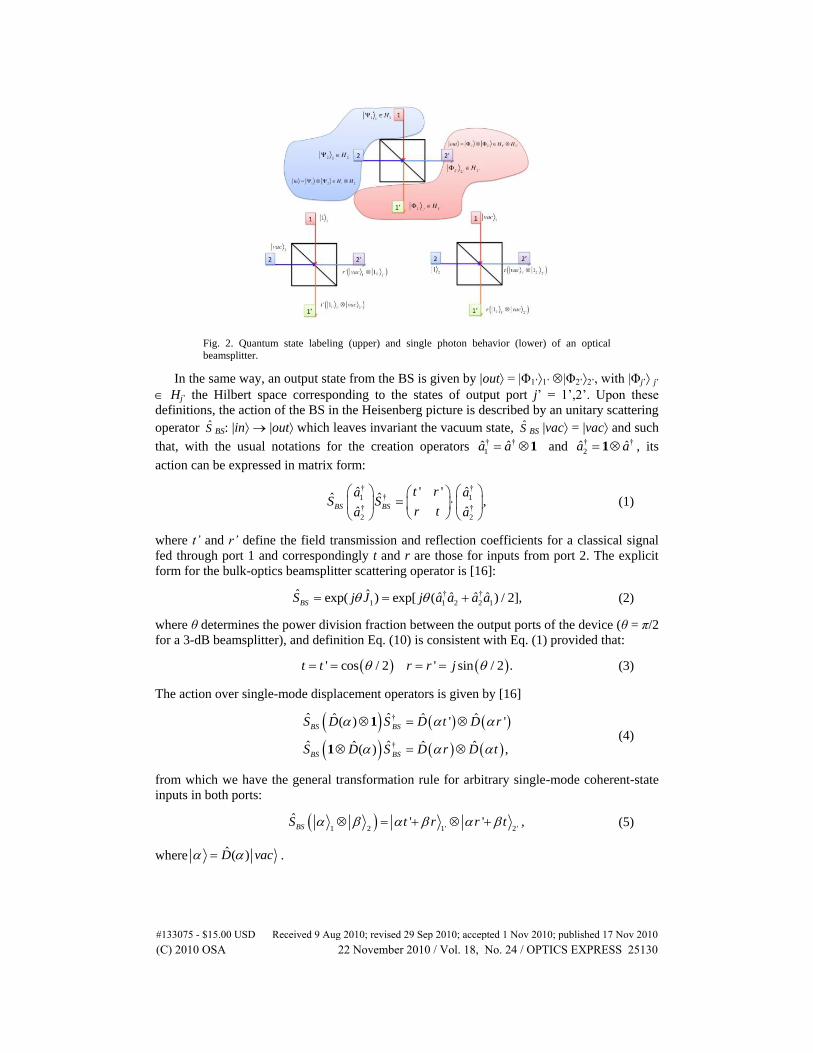
Fig. 2. Quantum state labeling (upper) and single photon behavior (lower) of an optical
beamsplitter.
In the same way, an output state from the BS is given by |out = |Φ1’1’ |Φ2’2’, with |Φj’ j’
Hj’ the Hilbert space corresponding to the states of output port j’ = 1’,2’. Upon these
definitions, the action of the BS in the Heisenberg picture is described by an unitary scattering
operator S BS: |in |out which leaves invariant the vacuum state, S BS |vac = |vac and such
that, with the usual notations for the creation operators † †
1ˆa a 1 and † †
2ˆ ˆa a 1 , its
action can be expressed in matrix form:
† †
†1 1
† †
2 2
' 'ˆ ˆˆ ˆ ,ˆ ˆ
BS BS
t ra aS S
r ta a
(1)
where t’ and r’ define the field transmission and reflection coefficients for a classical signal
fed through port 1 and correspondingly t and r are those for inputs from port 2. The explicit
form for the bulk-optics beamsplitter scattering operator is [16]:
† †
1 1 2 2 1ˆ ˆ ˆ ˆ ˆ ˆexp( ) exp[ ( ) / 2],BSS j J j a a a a (2)
where θ determines the power division fraction between the output ports of the device (θ = π/2
for a 3-dB beamsplitter), and definition Eq. (10) is consistent with Eq. (1) provided that:
' cos / 2 ' sin / 2 .t t r r j (3)
The action over single-mode displacement operators is given by [16]
†
†
ˆ ˆˆ ˆ ˆ( ) ' '
ˆ ˆˆ ˆ ˆ( ) ,
BS BS
BS BS
S D S D t D r
S D S D r D t
1
1 (4)
from which we have the general transformation rule for arbitrary single-mode coherent-state
inputs in both ports:
1 2 1' 2 '
ˆ ' ' ,BSS t r r t (5)
where ˆ ( )D vac .
#133075 - $15.00 USD Received 9 Aug 2010; revised 29 Sep 2010; accepted 1 Nov 2010; published 17 Nov 2010(C) 2010 OSA 22 November 2010 / Vol. 18, No. 24 / OPTICS EXPRESS 25130

2.2 Directional coupler
The most widespread version of the optical beamsplitter in guided-wave format is the
directional or 2 × 2 coupler [6–9]. It is composed on two input and two output optical fibers or
integrated input waveguides. Signal coupling is achieved on the central part of the device by
creating the adequate conditions such that the evanescent fields of the fundamental guided
mode in one waveguide can excite the fundamental guided mode in the other and vice-versa.
Different techniques to achieve signal coupling and for analyzing the device performance and
carry out a proper design have been developed in the last 20 years and are quite well known
and understood [6]. The beamsplitting power ratio of the 2 × 2 coupler is characterized by its
coupling constant k [6] that defines the fraction of power coupling (i.e crossing) from one
waveguide to the other. Another characteristic is the π/2 phase shift that the optical field
experiences when coupling from one waveguide to the other, which means that the reflection
coefficients r, r’ in Eq. (3) are imaginary. The results for the general bulk-optics beamsplitter
can thus be employed to describe the 2 × 2 directional coupler by making:
' 1 ' .t t k r r j k (6)
2.3 Y-branch power splitter
The Y-Branch or 1 × 2 Power Splitter is another popular guided-wave implementation of the
optical beamsplitter although it is more commonly employed in its integrated optics version
than in optical fiber format [8]. As the 2 × 2 directional coupler it is characterized by its
coupling constant k that again, defines the fraction of power coupling (i.e crossing) from one
waveguide to the other. However, in this case, there is no phase shift experienced by the
optical field when coupling from one waveguide to the other. The behavior of the Y-Branch
splitter under classical regime is shown in Fig. 3.
One distinctive feature of the Y-Branch is that it only has one physical input port. To
characterize the device as a beamsplitter [18], we need to assume that there is a second input
port although with no physical access from the classical point of view (on the reverse
operation this port corresponds to the radiated field due to the antisymmetric supermode [8]).
However, it should be borne in mind that under quantum regime this port is accessible by a
vacuum state [16].
Fig. 3. Classical behavior of Y-branch guided-wave power splitter.
The energy conservation and reciprocity relationships can be summarized as:
#133075 - $15.00 USD Received 9 Aug 2010; revised 29 Sep 2010; accepted 1 Nov 2010; published 17 Nov 2010(C) 2010 OSA 22 November 2010 / Vol. 18, No. 24 / OPTICS EXPRESS 25131

2 2 2 2 * *| ' | | ' | | | | | 1 ' ' 0.t r t r r t r t (7)
Now, if t, t’, r and r’ are real and k characterizes the fraction of power coupling (i.e crossing)
from one waveguide to the other then the above relationships are verified provided that:
' 1 ' ,t t k r k r (8)
so:
† †
†1 1
† †
2 2
1ˆ ˆˆ ˆ .ˆ ˆ1
YB YB
k ka aS S
a ak k
(9)
Alternatively, one can employ an explicit form for the Y-Branch power splitter scattering
operator, which in this case is given by a different expression than that of Eq. (2):
† †
2 1 2 2 1ˆ ˆ ˆ ˆ ˆ ˆexp( ) exp[ ( ) / 2].YBS j J a a a a (10)
Again, it can be checked that Eq. (10) verifies the transformation given by Eq. (9) if:
' 1 cos / 2 ' sin / 2 .t t k r r k (11)
2.4 Electro-optic phase modulator
Quantum models for the electro-optic phase modulator have been derived in detail in [20,21].
Figure 4 shows a typical layout of the device. It consists of a dielectric waveguide and two
electrodes placed at both sides. The dielectric material is subject to the electro-optic effect and
the voltage applied to the electrodes changes linearly the refractive index undergone by one of
the two possible input linear polarizations while not affecting the refractive index in the other
linear polarization.
Using the overcomplete basis of coherent states and by analogy with the classical behavior
it can be shown [21] that the modulator action subject to sinusoidal radiofrequency
modulation is described by a unitary operator S PM that couples modes with different
frequencies. Such modulating tone at frequency Ω is given by V(t) = VDC + Vmcos(Ωt +
θ).where φb = πVDC/Vπ is a static phase shift related to the modulator bias voltage normalized
by the modulator Vπ parameter, m = πVm/Vπ represents the radiofrequency modulation index.
The optical output shows frequencies ω0 + k Ω, with k the integer determining the order of the
output optical sideband. After quantizing the travelling-wave radiation in a length L, allowed
frequencies become multiples of the quantity 2π v/L, where v is the speed of light in the
medium. This implies that the incoming optical radiation can be described by index n0>0 such
that ω0 = 2π n0v/L, and correspondingly the radio-frequency Ω is determined by integer N>0
with Ω = 2π Nc/L. The scattering between waves with positive frequency is then given by:
0 0
†
0
† †
1
.ˆ ˆˆ ˆPM PM qn qN r
q
C qS a S a
(12)
Here the coefficients
00 0
0 0 00 ( ) ( ) 1 ( ) ( ) ( ),b bqj q q j q qj j
q q q q q q qC q e je J m J m e je J m
(13)
represent the scattering amplitudes from the input frequency represented by a mode number n0
= q0N r0 (q0 and r0 being integers with 0 r0<N) to an output mode of frequency qNr0. In
the last part of Eq. (13) we have introduced the so-called optical limit which recover the usual
expressions of the classical theory of electro-optic phase modulation: when the incoming
#133075 - $15.00 USD Received 9 Aug 2010; revised 29 Sep 2010; accepted 1 Nov 2010; published 17 Nov 2010(C) 2010 OSA 22 November 2010 / Vol. 18, No. 24 / OPTICS EXPRESS 25132

radiation is optical (n0>>0) the second Bessel function in Eq. (13) can be neglected and
Eq. (12) can be written as:
00
† †
1
† ˆ( ) ( ) ,ˆ ˆˆ b
o
j j s
PM PM s n sN
s q
n e je J m aS a S
(14)
and then Cq(q0) represents the amplitude of the scattering from the incoming frequency to its
sideband of order qq0.
Fig. 4. Typical configuration of a waveguide electro-optic phase modulator. (Lower) Black-box
representation of the phase modulator under quantum regime.
The phase modulator can be described by [21]:
* † ) ,ˆ ˆ ˆ ˆexp (PM N N b phS j T T N
(15)
where χ = ejθm/2 and
† †
0
1 1
ˆ ˆ ˆˆ ˆ ˆ ˆ ,N m N m ph m m
m m
T a a N T a a
(16)
3. General quantum model for the electro-optic amplitude modulator
We consider a general structure of the amplitude modulator as shown in Fig. 5. The layout is
obviously an abstract representation as the beamsplitters are of the guided wave type [5,6,8].
However, the representation of Fig. 5 clearly shows the three building blocks of the
modulator; an input beamsplitter opening the two paths of the interferometer, two different
paths (labeled 1 and 2 in the figure) which include, each one, a phase modulator and an output
beamsplitter which closes the interferometer and provides two possible output ports. Now, the
operator describing the action of the EOM, S EOM, is given by:
1 2
ˆ ˆ ˆ ˆ ˆ ˆ ˆ ˆ( ) ,o i o iEOM BS PM BS BS PM PM BSS S S S S S S S (17)
where S PM1 and S PM2 represent the scattering operators corresponding, respectively, to the
phase modulators located in the lower and upper paths of the layout of Fig. 5. S EOM is unitary,
since it is the product of three unitary operators, so that S EOM S†EOM = S
†EOM S EOM = 11.
We also mention that, although we use this complete layout to develop the model for the
amplitude modulator, the equations developed here can and will be particularized to the case
of asymmetric modulators as well where, say, S PM1 is substituted by the identity operator.
#133075 - $15.00 USD Received 9 Aug 2010; revised 29 Sep 2010; accepted 1 Nov 2010; published 17 Nov 2010(C) 2010 OSA 22 November 2010 / Vol. 18, No. 24 / OPTICS EXPRESS 25133
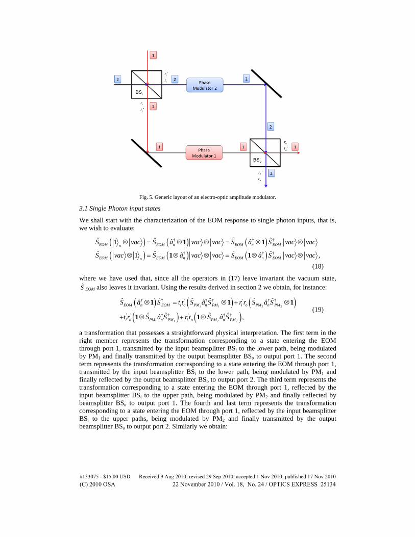
Fig. 5. Generic layout of an electro-optic amplitude modulator.
3.1 Single Photon input states
We shall start with the characterization of the EOM response to single photon inputs, that is,
we wish to evaluate:
† † †
† † †
ˆ ˆ ˆ ˆˆ ˆ1
ˆ ˆ ˆ ˆˆ ˆ1 ,
EOM EOM n EOM n EOMn
EOM EOM n EOM n EOMn
S vac S a vac vac S a S vac vac
S vac S a vac vac S a S vac vac
1 1
1 1
(18)
where we have used that, since all the operators in (17) leave invariant the vacuum state,
S EOM also leaves it invariant. Using the results derived in section 2 we obtain, for instance:
1 1 2 2
1 1 2 2
† † ' ' † † ' † †
' ' † † ' † †
ˆ ˆ ˆ ˆ ˆ ˆˆ ˆ ˆ
ˆ ˆ ˆ ˆˆ ˆ ,
EOM n EOM i o PM n PM i o PM n PM
i o PM n PM i o PM n PM
S a S t t S a S r r S a S
t r S a S r t S a S
1 1 1
1 1 (19)
a transformation that possesses a straightforward physical interpretation. The first term in the
right member represents the transformation corresponding to a state entering the EOM
through port 1, transmitted by the input beamsplitter BSi to the lower path, being modulated
by PM1 and finally transmitted by the output beamsplitter BSo to output port 1. The second
term represents the transformation corresponding to a state entering the EOM through port 1,
transmitted by the input beamsplitter BSi to the lower path, being modulated by PM1 and
finally reflected by the output beamsplitter BSo to output port 2. The third term represents the
transformation corresponding to a state entering the EOM through port 1, reflected by the
input beamsplitter BSi to the upper path, being modulated by PM2 and finally reflected by
beamsplitter BSo to output port 1. The fourth and last term represents the transformation
corresponding to a state entering the EOM through port 1, reflected by the input beamsplitter
BSi to the upper paths, being modulated by PM2 and finally transmitted by the output
beamsplitter BSo to output port 2. Similarly we obtain:
#133075 - $15.00 USD Received 9 Aug 2010; revised 29 Sep 2010; accepted 1 Nov 2010; published 17 Nov 2010(C) 2010 OSA 22 November 2010 / Vol. 18, No. 24 / OPTICS EXPRESS 25134
1 1 2 2
1 1 2 2
† † ' † † † †
' † † † †
ˆ ˆ ˆ ˆ ˆ ˆˆ ˆ ˆ
ˆ ˆ ˆ ˆˆ ˆ ,
EOM n EOM i o PM n PM i o PM n PM
i o PM n PM i o PM n PM
S a S rt S a S t r S a S
rr S a S t t S a S
1 1 1
1 1 (20)
with a similar physical interpretation for its four terms but taking into account that now the
input is in port 2. Although Eqs. (19) and (20) have been derived for a perfectly balanced
interferometer they hold for unbalanced structures since any phase imbalance between the
upper and the lower arms can be incorporated into the DC bias term φb.
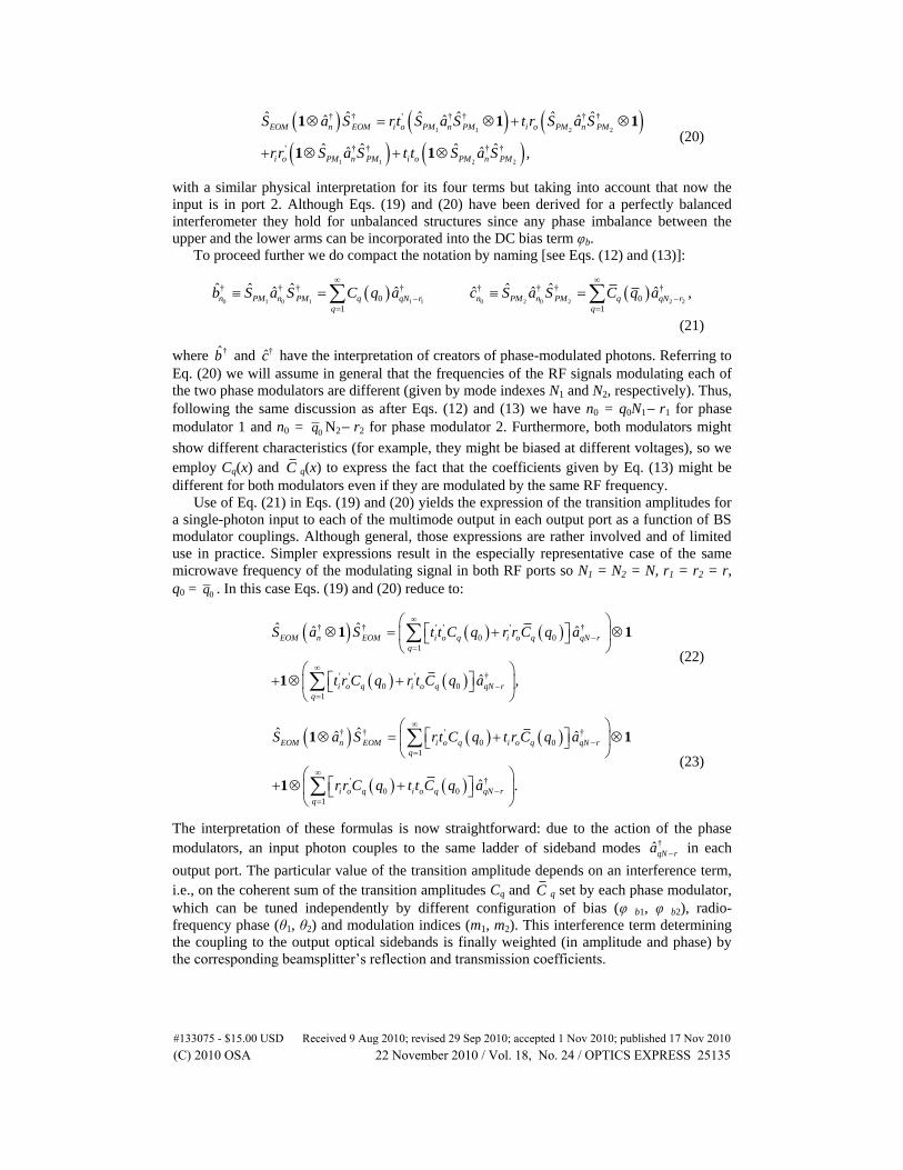
To proceed further we do compact the notation by naming [see Eqs. (12) and (13)]:
0 1 0 1 1 1 0 2 0 2 2 2
† † † † † † † †
0 0
1 1
ˆ ˆ ˆ ˆ ˆˆ ˆ ˆ ˆ ˆ ,n PM n PM q qN r n PM n PM q qN r
q q
b S a S C q a c S a S C q a
(21)
where †b and †c have the interpretation of creators of phase-modulated photons. Referring to
Eq. (20) we will assume in general that the frequencies of the RF signals modulating each of
the two phase modulators are different (given by mode indexes N1 and N2, respectively). Thus,
following the same discussion as after Eqs. (12) and (13) we have n0 = q0N1 r1 for phase
modulator 1 and n0 = 0q N2 r2 for phase modulator 2. Furthermore, both modulators might
show different characteristics (for example, they might be biased at different voltages), so we
employ Cq(x) and C q(x) to express the fact that the coefficients given by Eq. (13) might be
different for both modulators even if they are modulated by the same RF frequency.
Use of Eq. (21) in Eqs. (19) and (20) yields the expression of the transition amplitudes for
a single-photon input to each of the multimode output in each output port as a function of BS
modulator couplings. Although general, those expressions are rather involved and of limited
use in practice. Simpler expressions result in the especially representative case of the same
microwave frequency of the modulating signal in both RF ports so N1 = N2 = N, r1 = r2 = r,
q0 = 0q . In this case Eqs. (19) and (20) reduce to:
† † ' ' ' †
0 0
1
' ' ' †
0 0
1
ˆ ˆˆ ˆ
ˆ ,
EOM n EOM i o q i o q qN r
q
i o q i o q qN r
q
S a S t t C q r r C q a
t r C q r t C q a
1 1
1
(22)
† † ' †
0 0
1
' †
0 0
1
ˆ ˆˆ ˆ
ˆ .
EOM n EOM i o q i o q qN r
q
i o q i o q qN r
q
S a S rt C q t r C q a
r r C q t t C q a
1 1
1
(23)
The interpretation of these formulas is now straightforward: due to the action of the phase
modulators, an input photon couples to the same ladder of sideband modes †ˆqN ra in each
output port. The particular value of the transition amplitude depends on an interference term,
i.e., on the coherent sum of the transition amplitudes Cq and C q set by each phase modulator,
which can be tuned independently by different configuration of bias (φ b1, φ b2), radio-
frequency phase (θ1, θ2) and modulation indices (m1, m2). This interference term determining
the coupling to the output optical sidebands is finally weighted (in amplitude and phase) by
the corresponding beamsplitter’s reflection and transmission coefficients.
#133075 - $15.00 USD Received 9 Aug 2010; revised 29 Sep 2010; accepted 1 Nov 2010; published 17 Nov 2010(C) 2010 OSA 22 November 2010 / Vol. 18, No. 24 / OPTICS EXPRESS 25135
3.2 Coherent input states
In this case we need to evaluate:
0 0 0
0
00
†
†
ˆ ˆ ˆˆ( ) ( ( ) ) ( )
ˆ ˆ ˆˆ( ) ( ( )) ( ),o o
EOM n EOM n n EOMn
EOM n EOM n n EOMn
S vac S D S vac vac
S vac S D S vac vac
1
1 (24)
where |o on n represents the coherent state for mode number n0. We are thus interested in
computing the transformations. Following a similar procedure to that of subsection 3.1 we
arrive after a straightforward but lengthy process to:
0 0
1 1 0 2 2 1 1 2 2
†
' ' ' ' ' '
0 0 01 1
ˆ ˆˆ( ( ) )
ˆ ˆ ˆ ˆ ,o o o
EOM n n EOM
qN r n i o q qN r n i o q qN r n i o q o qN r n i o qq q
S D S
D t t C q D r r C q D t r C q D r t C q
1
(25)
where the brackets separate the multimode outputs in each of the two ports, and, similarly:
0 0
1 1 2 2 1 1 2 2
†
' '
0 0 0 01 1
ˆ ˆˆ( ( ))
ˆ ˆ ˆ ˆ( ) ( ) ( ) ( ) .o o o o
EOM n n EOM
qN r n i o q qN r n i o q qN r n i o q qN r n i o qq q
S D S
D rt C q D t r C q D rr C q D t t C q
1
(26)
Again, when the microwave frequency of the modulating signal is the same in both RF ports
(N1 = N2 = N, r1 = r2 = r, q0 = 0q ), the former equations reduce to:
0 0
0
†
' ' ' ' ' '
0 0 0 01 1
ˆ ˆˆ( ( ) )
ˆ ˆ( ) ( ) ( ) ( ) ,o
EOM n n EOM
qN r n i o q i o q qN r n i o q i o qq q
S D S
D t t C q r r C q D t r C q r t C q
1
(27)
0 0
0 0
†
' '
0 0 0 01 1
ˆ ˆˆ( ( ))
ˆ ˆ( ) ( ) ( ) ( ) .
EOM n n EOM
qN r n i o q i o q qN r n i o q i o qq q
S D S
D rt C q t r C q D rr C q t t C q
1
(28)
Comparison of Eqs. (27) and (28) with Eqs. (22) and (23) shows that the multimode coherent-
state outputs are governed by the same interference term or coherent sum of phase-modulator
settings (through Cq and C q) weighted by the beamsplitter reflection and transmission
coefficients. The situation is thus similar to that of a single beamsplitter or a passive
interferometer [16], where the classical output amplitudes described by the product states
Eqs. (27) and (28) are in direct correspondence of the transition amplitudes of the genuine
quantum output state Eqs. (22) and (23) when the modulator is operated at single-photon
level. In classical, coherent-state operation, the interference between modes is designed to
produce outputs with specific temporal features, such as pulse trains with different duty cycle
for digital communications or amplitude waveforms with distortion-free, linear response for
analog communications. At single-photon level, the action of the modulator is best viewed in
the spectral domain, where the device operates as an active, multimode beamsplitter, with
#133075 - $15.00 USD Received 9 Aug 2010; revised 29 Sep 2010; accepted 1 Nov 2010; published 17 Nov 2010(C) 2010 OSA 22 November 2010 / Vol. 18, No. 24 / OPTICS EXPRESS 25136
different output transition amplitudes that can be tuned by each of the phase-modulator
settings.
4. Particular results for selected EOM configurations
Despite the generality of the expressions developed in the previous section, in practical terms
however the range of amplitude modulators which are available either on the shelf or upon
request from manufacturers is restricted to a few number of designs, most of which have been
shown in Fig. 1. We now proceed to specialize the results obtained in 3.1 and 3.2 to those
configurations that are more commonly encountered in practice [5], restricting our analysis to
single-photon operation.
4.1 Y-Branch modulator with two modulating inputs
The layout of this modulator is shown in Fig. 1(A). In practical devices the design is such that:
' ' ' '1/ 2 1/ 2.o o i i i o i ot t t t r r r r (29)
Restricting the analysis to the case when the microwave frequency of the modulating signal is
the same in both RF ports, and a single-photon input at the only accessible port, we get
† † † †
0 0 0 0
1 1
1 1ˆ ˆˆ ˆ ˆ ,2 2oEOM n EOM q q qN r q q qN r
q q
S a S C q C q a C q C q a
1 1 1
(30)
with, according to Eq. (13)
1
2
01 0
0 0
02 0
0 0
0 1 1
0 2 2 .
( ) ( ) 1 ( )
( ) ( ) 1 ( )
b
b
q
q
qj q qjq q q q
qj q qjq q q q
C q ç
C q
e je J m J m
e je J m J m
(31)
Then, the response to a single photon input is given by:
0
0 0 0 0
1 1
1 1ˆ 1 ( ) ( ) 1 ( ) ( ) 1 .2 2
EOM q q q qn qN r qN rq q
S vac C q C q vac vac C q C q
(32)
Now, we specialize this output for two standard settings of this modulator through the
definition of bias, modulation indices and radio-frequency phase. The fist case is the so called
Double Sideband (DSB) operation in quadrature [4,5] which, due to the low harmonic
distortion represents one of the most standard setting in analog communications. It is
characterized by m1 = m2 = m, θ1 = 0, θ2 = π, φ b1 = φ b2 = π /2. Substituted into Eq. (31)
yields:
00
0 0
00
0 0
1
0
1 *
0 0
( )
( ) ( ),
( ) ( ) 1 ( )
( ) ( ) 1 ( )
q
q q
qq qq q q q
qq qq q q q
C q
C q C q
j J m J m
j J m J m
(33)
so Eq. (30) is now:
0
† † † †
0 0
1 1
ˆ ˆˆ ˆ ˆRe[ ( )] Im[ ( )] .EOM n EOM q qN r q qN r
q q
S a S C q a j C q a
1 1 1
(34)
#133075 - $15.00 USD Received 9 Aug 2010; revised 29 Sep 2010; accepted 1 Nov 2010; published 17 Nov 2010(C) 2010 OSA 22 November 2010 / Vol. 18, No. 24 / OPTICS EXPRESS 25137
The first term in the right member of Eq. (34) corresponds to the output field from the
modulator, while the second term identifies the radiated field. Turning our attention to the
output field term, we can see that the real part of Cq(q0) is zero if qqo is even. This means
that no modes corresponding to even harmonics are expected at the modulator output. This is
a well-known characteristic of this particular modulator design under classical operation.
The second interesting operation regime is the Single Sideband (SSB) operation [5] in
which by properly dephasing by 90° one of the input RF modulating tones one of the RF
sidebands (upper or lower) is eliminated at the output of the modulator. This operation mode
is also of widespread use in analog communication due to its resilience to link’s dispersion. In
this case the values of the parameters are m1 = m2 = m, θ1 = 0, θ2 = π/2, φ b1 = π/2 and φ b2 = 0,
substituted into Eq. (31) yields:
0 0
0 0
0 0
0 0
1
0
0
2 2( ) .
( ) ( ) ( 1) ( )
( ) ( ) ( 1) ( )
q
q
q q qq q q q
q q qq q q q
C q
C q
j J m J m
j J m J m
(35)
Note that for the special case when q = q01, that is, for the lower RF sideband one gets:
0 01 0 1 0 ,q qC q C q (36)
and thus, as expected, the contribution to the lower RF sideband is cancelled in the first term
of the right hand-side member of Eq. (32). It can be readily checked that the upper sideband is
cancelled if θ1 = 0, θ2 = π/2 while keeping unaltered the rest of the parameters.
4.2 Y-Branch modulator with one modulating input
The layout of this modulator is shown in Fig. 1(B), and its action can be derived from the
results of the previous subsection after substituting the action of the second phase modulator
PM2, which is not present, by the identity. Specifically:
0 1 0 1 0 1 0 1 0
1 1 0 1 1 0
† † † † † † † †
† † † †
0 0
1 1
1 1ˆ ˆ ˆ ˆ ˆ ˆˆ ˆ ˆ ˆ ˆ( ) ( ) ( )2 2
1 1ˆ ˆ ˆ ˆ( ) ( ) ,
2 2
EOM n EOM PM n PM n PM n PM n
q qN r n q qN r n
q q
S a S S a S a S a S a
C q a a C q a a
1 1 1
1 1
(37)
and the response to a single photon input is:
0 00 0
0 0
0 0
1,
0
1,
1ˆ 1 ( ( ) 1) 1 ( ) 12
1( ( ) 1) 1 1 .
2
o
o
EOM q qn n qN rq q q
q q on qN rq q q
S vac C q C q vac
vac C q C q
(38)
Here, except for the input mode index n0, the output is determined by the phase modulator
PM1 whose multimode output is split in the output beamsplitter. For n0, the output is
governed by the interference between the unmodulated photon and the phase-modulated
photon at mode n0, whose transition amplitude is 0 0( )qC q .
4.3 Hybrid Y-Branch modulator with two modulating inputs
The layout of this modulator is shown in Fig. 1(E), where:
#133075 - $15.00 USD Received 9 Aug 2010; revised 29 Sep 2010; accepted 1 Nov 2010; published 17 Nov 2010(C) 2010 OSA 22 November 2010 / Vol. 18, No. 24 / OPTICS EXPRESS 25138

' ' ' '1/ 2 / 2.o o i i i i o ot t t t r r r r j (39)
For this configuration, again, there is only one physically accessible input port (port 1), and
the former equation transforms to:
´0
† †
† †
0 0 0 0
1 1
ˆ ˆˆ( )
1 1ˆ ˆ( ) ( ) ( ) .
2 2
EOM n EOM
q q qN r q q qN r
q q
S a S
C q jC q a jC q C q a
1
1 1
(40)
Here, the interference terms produced in each sideband by the modulator represent the sum of
the transition amplitudes with an additional relative phase j.
5. Two-photon input
In the previous section, the focus has been the multimode transition capabilities of one-photon
states allowed by conventional designs of EOM. However, as interferometric devices with
control of the relative phase, modulation index and modulating driving tone in each arm,
EOMs permit compact implementations of standard, single-mode, quantum effects. In fact, if
the modulation indices of the phase modulators are set to zero, they behave as phase shifters
after the control of the bias voltage. Then, tasks based on bulk optics interferometers can be
directly translated to the DC modulators of type 1(C) and 1(D), since the four ports of the
interferometer are physically accessible and the mathematical descriptions of beamsplitter and
directional coupler are the same. However, proper selection and operation of the EOM permit
the integration in the same device of phase modulator and interferometer, thus allowing a
direct extension of certain operations to multimode, phase-modulated fields.
In this section we show how DC-modulators can be used to switch and interpolate
between two-port entangled and separable states composed of phase-modulated, multimode
photons. The transformation corresponding to an operator representing two input photons (one
at each input port) is given by:
´0 0 0 0
0 0 0 0 0 0 0 0
0 0 0 0
† † † † † † †
' ' ' † † ' ' ' † † ' ' ' † † ' † †
' † † ' † †
ˆ ˆ ˆ ˆ ˆ ˆˆ ˆ ˆ ˆ
ˆ ˆ ˆ ˆ ˆ ˆ ˆ ˆ2
ˆ ˆ ˆ ˆ2
EOM n n EOM EOM n EOM EOM n EOM
i o i o n n i o i o n n i o i o n n i o i o n n
i o i o n n i o i o n n
S a a S S a S S a S
t t r t b b t t r r b b t r r r b b r r t r c c
r r t t c c r t t t c c
1 1
1 1 1
1
0 0 0 0 0 0 0 0
' ' ' † † ' † † ' † † ' † †ˆ ˆ ˆ ˆˆ ˆ ˆ ˆ .i i i i o o n n o o n n o o n n o o n nt t r r r t b c t t b c r r c b t r b c
1 1
(41)
In practice the input beamsplitter to all modulators is always balanced, so that |ti| = |ti’| = |ri| =
|ri’| = 1/2 which, combined with the reciprocity relations, yields titi’ + riri’ = 0. This means
that both photons circulate in the same modulator’s arm due to the well-know effect [16].
Introducing in Eq. (41) the coefficients of the DC-modulators,
' ' ' '1/ 2 / 2,o o i i i i o ot t t t r r r r j (42)
we get:
´0 0 0 0 0 0 0 0
0 0 0 0 0 0
† † † † † † † † †
† † † † † †
1ˆ ˆ ˆ ˆ ˆ ˆˆ ˆˆ ˆ4 2 4
1ˆ ˆ ˆ ˆ ˆ ˆ ,
4 2 4
EOM n n EOM n n n n n n
n n n n n n
i iS a a S b b b b b b
i ic c c c c c
1 1
1 1
(43)
#133075 - $15.00 USD Received 9 Aug 2010; revised 29 Sep 2010; accepted 1 Nov 2010; published 17 Nov 2010(C) 2010 OSA 22 November 2010 / Vol. 18, No. 24 / OPTICS EXPRESS 25139

so that both output photons are modulated (scattered) by the same phase modulator.
Furthermore, if we consider set equal modulation indices and radio-frequency driving tones in
both phase modulators, we get † †ˆˆ exp( )
o on b nc j b , where Δφb represents the bias voltage
difference between the upper and lower phase modulators, we obtain
´0 0
0 0 0 0 0 0
† † †
† † † † † †
ˆ ˆˆ ˆ
ˆ ˆ ˆ ˆ ˆ ˆsin [ ] cos( ) .2
b
b
EOM n n EOM
jj
b n n n n b n n
S a a S
eb b b b e b b
1 1
(44)
Now, the structure of the output state can be controlled by Δφb. For instance, if Δφb = 0 then
the output is a product state, whereas for Δφb = π/2 the output state is entangled, and at this
point the overall modulator behaves in a similar fashion to a balanced beamsplitter acting on
phase-modulated states.
6. Multitone amplitude modulation
We turn now our attention to the modeling of the EOM subject to multitone RF signal
modulation as we previously considered in [21] for the electro-optic phase modulator. The
interest in this analysis is justified by the fact that this is the regime under which several
quantum experimental setups [10] and subcarrier multiplexed quantum key distribution
systems [4,22], operate. We will assume, as in [21] linear and small signal modulation
conditions, that is, m <<1.
In principle, the general expressions [Eqs. (17)–(20)] are valid but Eq. (20) has to be
modified according to Eq. (49) of [21] to:
1 1 1 1
0 1 0 1 0 0 1 0 1
2 2 2 2
0 1 0 1 0 0 2 0 2
† † † † † †
1
1
† † † † † †
2
1
ˆ ˆ ˆˆ ˆ ˆ ˆ
ˆ ˆˆ ˆ ˆ ˆ ˆ .
b b k k
k k
b b k k
k k
Mj j j j
n PM n PM n k n N n N
k
Mj j j j
n PM n PM n k n N n N
k
b S a S e a e m je a je a
c S a S e a e m je a je a
(45)
Here M stands for the number of RF tones in the modulating signal. For SCM-QKD systems
in particular we are principally interested in the behavior under a coherent state input, since
this is the state characterizing the output of a faint pulsed laser source. For this case we can
follow the same process as in section 5 of [21] and sections 3 and 4 but taking into account the
prescriptions given by Eq. (45) to find:
0 0
1 2 1 1 2 2
0 0 0 1 0 0 2 0
1 2
0 0 0 1 0
†
' ' ' ' ' '
1 21
' ' ' ' '
11
ˆ ˆ ˆˆ ˆ
ˆ ˆ ˆ ˆ
ˆ ˆ ˆ
b b b k b k
k k
b b
k
EOM n n EOM
Mj j j j j j
n n i o i o n N i o k n n N i o k nk
Nj j
n n i o i o n N i o k nk
S D S A B
A D t t e r r e D t t m j e e D r r m j e e
B D t r e r t e D t r m j
1
1 1 2 2
0 2 0
'
2ˆ ,b k b k
k
j j j j
n N i o k ne e D r t m j e e
(46)
and:
0 0
1 2 1 1 2 2
0 0 0 1 0 0 2 0
1 2 1
0 0 0 1 0
†
' '
1 21
' '
11
ˆ ˆˆ ˆ ˆ
ˆ ˆ ˆ ˆ
ˆ ˆ ˆ
b b b k b k
k k
b b b
k
EOM n n EOM
Mj j j j j j
n n i o i o n N i o k n n N i o k nk
Nj j j
n n i o i o n N i o k nk
S D S E F
E D rt e t r e D rt m j e e D t r m j e e
F D r r e t t e D r r m j e e
1
1 2 2
0 2 02ˆ .k b k
k
j j j
n N i o k nD t t m j e e
(47)
#133075 - $15.00 USD Received 9 Aug 2010; revised 29 Sep 2010; accepted 1 Nov 2010; published 17 Nov 2010(C) 2010 OSA 22 November 2010 / Vol. 18, No. 24 / OPTICS EXPRESS 25140

The former expressions can be simplified if the same microwave modulation frequencies are
assumed for both RF ports. In this case:
1 2 1 1 2 2
0 0 0
1 2 1 1 2 2
0 0 0
0
' ' ' ' ' '
1 21
' ' ' ' ' '
1 21
ˆ ˆ ˆ
ˆ ˆ ˆ
ˆ ˆ
b b b k b k
k o
b b b k b k
k o
Mj j j j j j
n n i o i o n N n i o k i o kk
Mj j j j j j
n n i o i o n N n i o k i o kk
n
A D t t e r r e D j t t m e e r r m e e
B D t r e r t e D j t r m e e r t m e e
E D
1 2 1 1 2 2
0 0
1 2 1 1 2 2
0 0 0
' '
1 21
' '
1 21
ˆ
ˆ ˆ ˆ .
b b b k b k
k o
b b b k b k
k o
Mj j j j j j
n i o i o n N n i o k i o kk
Mj j j j j j
n n i o i o n N n i o k i o kk
r t e t r e D j r t m e e t r m e e
F D r r e t t e D j r r m e e t t m e e
(48)
These expressions are obviously general and can be particularized to the different modulator
designs as we did in Section 4.
It is useful to compute the value of the mean fields corresponding to Eqs. (46)–(48). To do
so we will assume that the input coherent state is fed to only one of the device ports (port 1)
and assume equal modulation frequencies at both ports. In such a case, the output state is
given by:
0 00
1 2 1 1 2 2
0 00
1 2
0 00
†
1 21 2
' ' ' ' ' '
1 1 21 1
' ' ' ' '
2 12 1
ˆ ˆ ˆˆ( ( ) )
( ) ( )
( ) (
o
b b b k b k
o k
b b
EOM n EOM n n EOMn
Mj j j j j j
n i o i o n i o k i o kn n Nk
Mj j j
n i o i o n i o kn k
S vac S D S vac vac
t t e r r e j t t m e e r r m e e
t r e r t e j t r m e
1
1 1 2 2'
2 ) .b k b k
o k
j j j
i o kn N
e r t m e e
(49)
To evaluate the mean field at the output port 1 of the modulator we consider the electric field
operator given by [16]:
1ˆ ˆ ,
2
j t
o
E j a eV
x 1 (50)
where x is the unit vector relevant polarization. Then, applied to Eq. (51), yields an average
field:
1 2 0
0
01 1 2 2
0
' ' '
1 0
' ' '
0 1 2
1
ˆ
.
b b
kb k b k
j j j t
n i o i o
Mj tj j j j
k n i o k i o k
k
E hc j t t e r r e e
j j t t m e e r r m e e e cc
x
x (51)
Equation (51) shows the presence of photons in the mode corresponding to the input coherent
state as well as in the sidebands corresponding to the M modulating RF subcarriers.
6. Summary and conclusions
We have presented a quantum model for electro-optic amplitude modulation, which is built
upon quantum models of the main photonic components that constitute the EOM, that is, the
guided-wave beamsplitter and the electro-optic phase modulator and accounts for all the
different modulator structures which are currently available. General models have been
developed both for single and dual drive configurations and specific results were obtained for
the most common configurations currently employed. Finally, the operation with two-photon
input for the control of phase-modulated photons and the important topic of multicarrier
modulation are also addressed.
#133075 - $15.00 USD Received 9 Aug 2010; revised 29 Sep 2010; accepted 1 Nov 2010; published 17 Nov 2010(C) 2010 OSA 22 November 2010 / Vol. 18, No. 24 / OPTICS EXPRESS 25141

Acknowledgements
The authors wish to acknowledge the financial support of the Spanish Government through
Project TEC2008-02606 and Project Quantum Optical Information Technology (QOIT), a
CONSOLIDER-INGENIO 2010 Project; and also the Generalitat Valenciana through the
PROMETEO research excellency award programme GVA PROMETEO 2008/092.
#133075 - $15.00 USD Received 9 Aug 2010; revised 29 Sep 2010; accepted 1 Nov 2010; published 17 Nov 2010(C) 2010 OSA 22 November 2010 / Vol. 18, No. 24 / OPTICS EXPRESS 25142